EP3214758A1 - Methods for mapping power generation installations - Google Patents
Methods for mapping power generation installations Download PDFInfo
- Publication number
- EP3214758A1 EP3214758A1 EP17158978.1A EP17158978A EP3214758A1 EP 3214758 A1 EP3214758 A1 EP 3214758A1 EP 17158978 A EP17158978 A EP 17158978A EP 3214758 A1 EP3214758 A1 EP 3214758A1
- Authority
- EP
- European Patent Office
- Prior art keywords
- devices
- power
- components
- installation
- map
- Prior art date
- Legal status (The legal status is an assumption and is not a legal conclusion. Google has not performed a legal analysis and makes no representation as to the accuracy of the status listed.)
- Granted
Links
- 238000000034 method Methods 0.000 title claims abstract description 197
- 238000009434 installation Methods 0.000 title claims abstract description 100
- 238000013507 mapping Methods 0.000 title description 21
- 238000010248 power generation Methods 0.000 title description 5
- 230000008859 change Effects 0.000 claims description 9
- 238000005516 engineering process Methods 0.000 claims description 6
- 230000004044 response Effects 0.000 claims description 5
- 238000001514 detection method Methods 0.000 claims description 4
- 238000005259 measurement Methods 0.000 description 49
- 238000004891 communication Methods 0.000 description 43
- 238000010586 diagram Methods 0.000 description 25
- 238000007726 management method Methods 0.000 description 9
- 230000004807 localization Effects 0.000 description 7
- 239000003550 marker Substances 0.000 description 7
- 238000012544 monitoring process Methods 0.000 description 6
- 230000008901 benefit Effects 0.000 description 4
- 239000004020 conductor Substances 0.000 description 4
- 238000013461 design Methods 0.000 description 4
- 230000006870 function Effects 0.000 description 4
- 238000012423 maintenance Methods 0.000 description 4
- 238000004519 manufacturing process Methods 0.000 description 4
- 230000008569 process Effects 0.000 description 4
- 238000012545 processing Methods 0.000 description 4
- 208000032750 Device leakage Diseases 0.000 description 3
- 239000003990 capacitor Substances 0.000 description 3
- 230000008878 coupling Effects 0.000 description 3
- 238000010168 coupling process Methods 0.000 description 3
- 238000005859 coupling reaction Methods 0.000 description 3
- 238000012806 monitoring device Methods 0.000 description 3
- 230000001413 cellular effect Effects 0.000 description 2
- 238000001914 filtration Methods 0.000 description 2
- 230000004048 modification Effects 0.000 description 2
- 238000012986 modification Methods 0.000 description 2
- 238000005457 optimization Methods 0.000 description 2
- 238000012360 testing method Methods 0.000 description 2
- 238000001931 thermography Methods 0.000 description 2
- WCUXLLCKKVVCTQ-UHFFFAOYSA-M Potassium chloride Chemical compound [Cl-].[K+] WCUXLLCKKVVCTQ-UHFFFAOYSA-M 0.000 description 1
- 238000002070 Raman circular dichroism spectroscopy Methods 0.000 description 1
- 241000218220 Ulmaceae Species 0.000 description 1
- 230000004913 activation Effects 0.000 description 1
- 238000004458 analytical method Methods 0.000 description 1
- 238000003491 array Methods 0.000 description 1
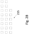
- 230000005540 biological transmission Effects 0.000 description 1
- 238000009529 body temperature measurement Methods 0.000 description 1
- 238000004364 calculation method Methods 0.000 description 1
- 230000010267 cellular communication Effects 0.000 description 1
- 239000003086 colorant Substances 0.000 description 1
- 230000009849 deactivation Effects 0.000 description 1
- 230000003247 decreasing effect Effects 0.000 description 1
- 230000001934 delay Effects 0.000 description 1
- 230000003111 delayed effect Effects 0.000 description 1
- 230000004069 differentiation Effects 0.000 description 1
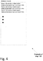
- 230000008030 elimination Effects 0.000 description 1
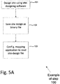
- 238000003379 elimination reaction Methods 0.000 description 1
- 230000007613 environmental effect Effects 0.000 description 1
- 239000000446 fuel Substances 0.000 description 1
- 230000006872 improvement Effects 0.000 description 1
- 230000007257 malfunction Effects 0.000 description 1
- 238000013439 planning Methods 0.000 description 1
- 239000013316 polymer of intrinsic microporosity Substances 0.000 description 1
- 230000009467 reduction Effects 0.000 description 1
- 238000002310 reflectometry Methods 0.000 description 1
- 238000002922 simulated annealing Methods 0.000 description 1
- 230000001131 transforming effect Effects 0.000 description 1
- 230000001960 triggered effect Effects 0.000 description 1
- 238000013024 troubleshooting Methods 0.000 description 1
- 238000010200 validation analysis Methods 0.000 description 1
Images


Classifications
-
- G—PHYSICS
- G01—MEASURING; TESTING
- G01S—RADIO DIRECTION-FINDING; RADIO NAVIGATION; DETERMINING DISTANCE OR VELOCITY BY USE OF RADIO WAVES; LOCATING OR PRESENCE-DETECTING BY USE OF THE REFLECTION OR RERADIATION OF RADIO WAVES; ANALOGOUS ARRANGEMENTS USING OTHER WAVES
- G01S19/00—Satellite radio beacon positioning systems; Determining position, velocity or attitude using signals transmitted by such systems
- G01S19/38—Determining a navigation solution using signals transmitted by a satellite radio beacon positioning system
- G01S19/39—Determining a navigation solution using signals transmitted by a satellite radio beacon positioning system the satellite radio beacon positioning system transmitting time-stamped messages, e.g. GPS [Global Positioning System], GLONASS [Global Orbiting Navigation Satellite System] or GALILEO
- G01S19/42—Determining position
- G01S19/45—Determining position by combining measurements of signals from the satellite radio beacon positioning system with a supplementary measurement
- G01S19/46—Determining position by combining measurements of signals from the satellite radio beacon positioning system with a supplementary measurement the supplementary measurement being of a radio-wave signal type
-
- G—PHYSICS
- G06—COMPUTING; CALCULATING OR COUNTING
- G06K—GRAPHICAL DATA READING; PRESENTATION OF DATA; RECORD CARRIERS; HANDLING RECORD CARRIERS
- G06K7/00—Methods or arrangements for sensing record carriers, e.g. for reading patterns
- G06K7/10—Methods or arrangements for sensing record carriers, e.g. for reading patterns by electromagnetic radiation, e.g. optical sensing; by corpuscular radiation
- G06K7/14—Methods or arrangements for sensing record carriers, e.g. for reading patterns by electromagnetic radiation, e.g. optical sensing; by corpuscular radiation using light without selection of wavelength, e.g. sensing reflected white light
- G06K7/1404—Methods for optical code recognition
- G06K7/1408—Methods for optical code recognition the method being specifically adapted for the type of code
- G06K7/1413—1D bar codes
-
- G—PHYSICS
- G05—CONTROLLING; REGULATING
- G05B—CONTROL OR REGULATING SYSTEMS IN GENERAL; FUNCTIONAL ELEMENTS OF SUCH SYSTEMS; MONITORING OR TESTING ARRANGEMENTS FOR SUCH SYSTEMS OR ELEMENTS
- G05B19/00—Programme-control systems
- G05B19/02—Programme-control systems electric
- G05B19/04—Programme control other than numerical control, i.e. in sequence controllers or logic controllers
- G05B19/042—Programme control other than numerical control, i.e. in sequence controllers or logic controllers using digital processors
-
- G—PHYSICS
- G06—COMPUTING; CALCULATING OR COUNTING
- G06F—ELECTRIC DIGITAL DATA PROCESSING
- G06F17/00—Digital computing or data processing equipment or methods, specially adapted for specific functions
- G06F17/10—Complex mathematical operations
- G06F17/11—Complex mathematical operations for solving equations, e.g. nonlinear equations, general mathematical optimization problems
-
- G—PHYSICS
- G06—COMPUTING; CALCULATING OR COUNTING
- G06K—GRAPHICAL DATA READING; PRESENTATION OF DATA; RECORD CARRIERS; HANDLING RECORD CARRIERS
- G06K7/00—Methods or arrangements for sensing record carriers, e.g. for reading patterns
- G06K7/10—Methods or arrangements for sensing record carriers, e.g. for reading patterns by electromagnetic radiation, e.g. optical sensing; by corpuscular radiation
- G06K7/10009—Methods or arrangements for sensing record carriers, e.g. for reading patterns by electromagnetic radiation, e.g. optical sensing; by corpuscular radiation sensing by radiation using wavelengths larger than 0.1 mm, e.g. radio-waves or microwaves
- G06K7/10366—Methods or arrangements for sensing record carriers, e.g. for reading patterns by electromagnetic radiation, e.g. optical sensing; by corpuscular radiation sensing by radiation using wavelengths larger than 0.1 mm, e.g. radio-waves or microwaves the interrogation device being adapted for miscellaneous applications
-
- H—ELECTRICITY
- H01—ELECTRIC ELEMENTS
- H01L—SEMICONDUCTOR DEVICES NOT COVERED BY CLASS H10
- H01L31/00—Semiconductor devices sensitive to infrared radiation, light, electromagnetic radiation of shorter wavelength or corpuscular radiation and specially adapted either for the conversion of the energy of such radiation into electrical energy or for the control of electrical energy by such radiation; Processes or apparatus specially adapted for the manufacture or treatment thereof or of parts thereof; Details thereof
- H01L31/02—Details
- H01L31/02002—Arrangements for conducting electric current to or from the device in operations
- H01L31/02005—Arrangements for conducting electric current to or from the device in operations for device characterised by at least one potential jump barrier or surface barrier
- H01L31/02008—Arrangements for conducting electric current to or from the device in operations for device characterised by at least one potential jump barrier or surface barrier for solar cells or solar cell modules
- H01L31/0201—Arrangements for conducting electric current to or from the device in operations for device characterised by at least one potential jump barrier or surface barrier for solar cells or solar cell modules comprising specially adapted module bus-bar structures
-
- H—ELECTRICITY
- H01—ELECTRIC ELEMENTS
- H01L—SEMICONDUCTOR DEVICES NOT COVERED BY CLASS H10
- H01L31/00—Semiconductor devices sensitive to infrared radiation, light, electromagnetic radiation of shorter wavelength or corpuscular radiation and specially adapted either for the conversion of the energy of such radiation into electrical energy or for the control of electrical energy by such radiation; Processes or apparatus specially adapted for the manufacture or treatment thereof or of parts thereof; Details thereof
- H01L31/02—Details
- H01L31/0224—Electrodes
- H01L31/022408—Electrodes for devices characterised by at least one potential jump barrier or surface barrier
- H01L31/022425—Electrodes for devices characterised by at least one potential jump barrier or surface barrier for solar cells
- H01L31/022433—Particular geometry of the grid contacts
-
- H—ELECTRICITY
- H01—ELECTRIC ELEMENTS
- H01L—SEMICONDUCTOR DEVICES NOT COVERED BY CLASS H10
- H01L31/00—Semiconductor devices sensitive to infrared radiation, light, electromagnetic radiation of shorter wavelength or corpuscular radiation and specially adapted either for the conversion of the energy of such radiation into electrical energy or for the control of electrical energy by such radiation; Processes or apparatus specially adapted for the manufacture or treatment thereof or of parts thereof; Details thereof
- H01L31/04—Semiconductor devices sensitive to infrared radiation, light, electromagnetic radiation of shorter wavelength or corpuscular radiation and specially adapted either for the conversion of the energy of such radiation into electrical energy or for the control of electrical energy by such radiation; Processes or apparatus specially adapted for the manufacture or treatment thereof or of parts thereof; Details thereof adapted as photovoltaic [PV] conversion devices
- H01L31/042—PV modules or arrays of single PV cells
- H01L31/05—Electrical interconnection means between PV cells inside the PV module, e.g. series connection of PV cells
- H01L31/0504—Electrical interconnection means between PV cells inside the PV module, e.g. series connection of PV cells specially adapted for series or parallel connection of solar cells in a module
-
- H—ELECTRICITY
- H02—GENERATION; CONVERSION OR DISTRIBUTION OF ELECTRIC POWER
- H02S—GENERATION OF ELECTRIC POWER BY CONVERSION OF INFRARED RADIATION, VISIBLE LIGHT OR ULTRAVIOLET LIGHT, e.g. USING PHOTOVOLTAIC [PV] MODULES
- H02S50/00—Monitoring or testing of PV systems, e.g. load balancing or fault identification
-
- G—PHYSICS
- G05—CONTROLLING; REGULATING
- G05B—CONTROL OR REGULATING SYSTEMS IN GENERAL; FUNCTIONAL ELEMENTS OF SUCH SYSTEMS; MONITORING OR TESTING ARRANGEMENTS FOR SUCH SYSTEMS OR ELEMENTS
- G05B2219/00—Program-control systems
- G05B2219/20—Pc systems
- G05B2219/26—Pc applications
- G05B2219/2639—Energy management, use maximum of cheap power, keep peak load low
-
- Y—GENERAL TAGGING OF NEW TECHNOLOGICAL DEVELOPMENTS; GENERAL TAGGING OF CROSS-SECTIONAL TECHNOLOGIES SPANNING OVER SEVERAL SECTIONS OF THE IPC; TECHNICAL SUBJECTS COVERED BY FORMER USPC CROSS-REFERENCE ART COLLECTIONS [XRACs] AND DIGESTS
- Y02—TECHNOLOGIES OR APPLICATIONS FOR MITIGATION OR ADAPTATION AGAINST CLIMATE CHANGE
- Y02E—REDUCTION OF GREENHOUSE GAS [GHG] EMISSIONS, RELATED TO ENERGY GENERATION, TRANSMISSION OR DISTRIBUTION
- Y02E10/00—Energy generation through renewable energy sources
- Y02E10/50—Photovoltaic [PV] energy
Landscapes
- Engineering & Computer Science (AREA)
- Physics & Mathematics (AREA)
- General Physics & Mathematics (AREA)
- Theoretical Computer Science (AREA)
- Electromagnetism (AREA)
- Toxicology (AREA)
- Health & Medical Sciences (AREA)
- Mathematical Physics (AREA)
- Pure & Applied Mathematics (AREA)
- Mathematical Analysis (AREA)
- Data Mining & Analysis (AREA)
- Computer Vision & Pattern Recognition (AREA)
- Artificial Intelligence (AREA)
- Computational Mathematics (AREA)
- General Health & Medical Sciences (AREA)
- Mathematical Optimization (AREA)
- Radar, Positioning & Navigation (AREA)
- Computer Hardware Design (AREA)
- Power Engineering (AREA)
- Microelectronics & Electronic Packaging (AREA)
- Condensed Matter Physics & Semiconductors (AREA)
- Sustainable Development (AREA)
- Remote Sensing (AREA)
- Life Sciences & Earth Sciences (AREA)
- Algebra (AREA)
- Databases & Information Systems (AREA)
- Operations Research (AREA)
- Software Systems (AREA)
- General Engineering & Computer Science (AREA)
- Sustainable Energy (AREA)
- Automation & Control Theory (AREA)
- Computer Networks & Wireless Communication (AREA)
- Position Fixing By Use Of Radio Waves (AREA)
- Remote Monitoring And Control Of Power-Distribution Networks (AREA)
- Photovoltaic Devices (AREA)
Abstract
Description
- The present application claims priority to
U.S. provisional patent application Ser. No. 62/303,017, filed Mar. 3, 2016 U.S. provisional patent application Ser. No. 62/381,298, filed Aug. 30, 2016 -
- 1. Photovoltaic (PV) installations may include a large number of components and wide variety of devices. A PV installation may include one or more arrays of PV generators (e.g. solar modules, solar cells, solar panels), one or more inverter(s), communication devices, and PV power devices such DC/DC converters, DC-AC microinverters, combiner boxes, and Maximum-Power-Point-Tracking (MPPT) devices. Some installations may further include batteries. Some of the electronic modules may be integrated with the PV modules and may provide other functions such as monitoring of performance and/or protection against theft. In case of the system experiencing power loss or in case of a potentially unsafe condition, it may be desirable for a system maintenance operator to physically locate a particular device (e.g. solar panel, DC-DC converter or micro-inverter) that may be potentially responsible for the power loss or potentially unsafe condition.
- 2. Operators and monitoring bodies of PV installations might not always have access to a map which indicates the location of each PV module, identified by a serial number. In such cases, troubleshooting problems may be time consuming, since locating a specific module, e.g., a malfunctioning module, may be difficult. In other instances, a map of the installation may be obtained by significant manual effort, such as a maintenance worker walking through the installation and copying ID numbers off modules, denoting their location on a map. If performed manually, human error may also cause inaccurate information to be recorded in the maps.
- 3. There is a need for an automatic or semi-automatic method of generating physical maps of PV installations, to save work and reduce errors, while allowing system monitoring personnel to obtain the benefits of having a map which indicates the locations and ID numbers of PV modules.
-
- 4. The following summary is a short summary of some of the inventive concepts for illustrative purposes only, and is not intended to limit or constrain the inventions and examples in the detailed description. One skilled in the art will recognize other novel combinations and features from the detailed description.
- 5. Embodiments herein may employ methods for generating maps of PV installations. Some illustrative embodiments may be fully automatic, and some may require manual steps.
- 6. In illustrative methods, a suitable localization algorithm may be utilized to measure or estimate the global coordinates of photovoltaic (PV) devices, and/or the distance and/or angle between different devices, and/or the distance and/or angle between devices and known locations. Some embodiments may include obtaining the global coordinates of devices. Some embodiments may produce a map displaying the physical placement and location of devices along with identifying information (e.g. ID or serial numbers). Some embodiments may utilize high-accuracy Global Positioning System (GPS) technology to map the installation. For example, some illustrative methods may include scanning an identifying barcode on PV devices while using GPS to obtain the global coordinates at each scanned location. In some embodiments, a map not including identifying module information may be further utilized to match specific modules to the measured GPS coordinates. Some embodiments may include PV devices transmitting and receiving wireless signals from one another, and using measured or estimated quantities such as Received Signal Strength Indication (RSSI), Angle of Arrival (AOA, also known as Direction of Arrival, or DOA) and/or Time Difference of Arrival (TDOA) to estimate relative distances and/or angles between modules. In some embodiments, Power Line Communication (PLC) methods may be used along with Time Domain Reflection (TDR) techniques to estimate the location of a set of PV devices within a PV installation. The set of estimates may be processed to obtain an accurate physical map of the installation, including identifying where each PV module and/or PV device is physically located.
- 7. In other illustrative methods, photovoltaic modules may be operated to increase and decrease the electrical power produced by the photovoltaic modules, which may result in a change of temperature at the photovoltaic modules. A thermal imaging device may be used to capture thermal images of a group of photovoltaic modules under different power production and temperature conditions, and suitable methods may analyze and aggregate the thermal images to obtain an accurate physical map of the installation.
- 8. As noted above, this summary is merely a summary of some of the features described herein. It is not exhaustive, and it is not to be a limitation on the claims.
-
- 9. These and other features, aspects, and advantages of the present disclosure will become better understood with regard to the following description, claims, and drawings. The present disclosure is illustrated by way of example, and not limited by, the accompanying figures. A more complete understanding of the present disclosure and the advantages thereof may be acquired by referring to the following description in consideration of the accompanying drawings, in which like reference numbers indicate like features, and wherein:
- 10.
Fig. 1 is a flow diagram of a method for generating a photovoltaic (PV) installation map according to one or more illustrative aspects of the disclosure. - 11.
Fig. 2A is a flow diagram of a method for fitting measured locations to a map according to one or more illustrative aspects of the disclosure. - 12.
Fig. 2B illustrates a non-identifying map (NIM) according to one or more illustrative aspects of the disclosure. - 13.
Fig. 2C illustrates an estimated layout map (ELM) according to one or more illustrative aspects of the disclosure. - 14.
Fig. 2D illustrates how illustrative methods may be applied to illustrative PV systems according to one or more illustrative aspects of the disclosure. - 15.
Fig. 3A is a flow diagram of a method for generating an installation map based on time and location according to one or more illustrative aspects of the disclosure. - 16.
Fig. 3B is a flow diagram of a method for mapping samples to strings according to one or more illustrative aspects of the disclosure. - 17.
Fig. 4 illustrates an illustrative of representing and storing a Non-Identifying Map according to one or more illustrative aspects of the disclosure. - 18.
Fig. 5A is a flow diagram of a method for generating a Non-Identifying Map according to one or more illustrative aspects of the disclosure. - 19.
Fig. 5B illustrates a user interface for PV installation mapping according to one or more illustrative aspects of the disclosure. - 20.
Fig. 6 illustrates an illustrative embodiment of reading identifying information from a PV device and estimating the device location according to one or more illustrative aspects of the disclosure. - 21.
Fig. 7 illustrates illustrative devices which may be used for reading identifying information and/or estimating device location according to one or more illustrative aspects of the disclosure. - 22.
Fig. 8A is a flow diagram of a method for installation mapping according to one or more illustrative aspects of the disclosure. - 23.
Fig. 8B illustrates results of various stages of installation mapping according to one or more illustrative aspects of the disclosure. - 24.
Fig. 9 is part-block diagram, part schematic of an illustrative PV installation that may be mapped according to one or more illustrative aspects of the disclosure. - 25.
Fig. 10 is a flow diagram of a method for grouping power devices into groups according to one or more illustrative aspects of the disclosure. - 26.
Fig. 11A is a part-block diagram, part-schematic of PV system components which may be used in conjunction with methods described herein. - 27.
Fig. 11B is a schematic of illustrative variable impedance circuits according to one or more illustrative aspects of the disclosure. - 28.
Fig. 12 illustrates an illustrative form of a wave reflected off a transmission line according to one or more illustrative aspects of the disclosure. - 29.
Fig. 13 is a flow diagram of a method for testing power devices according to one or more illustrative aspects of the disclosure. - 30.
Fig. 14 is a part-block diagram, part-schematic of a PV arrangement, comprising PV system components, which may be used in conjunction with methods described herein. - 31.
Fig. 15A is a part-block diagram, part-schematic of a PV panel and PV system components which may be used in conjunction with methods described herein. - 32.
Fig. 15B is a part-block diagram, part-schematic of PV system components which may be used in conjunction with methods described herein. - 33.
Fig. 16 is a flow diagram of a method for grouping power devices into strings according to one or more illustrative aspects of the disclosure. - 34.
Fig. 17A illustrates an illustrative PV string of PV devices according to one or more illustrative aspects of the disclosure. - 35.
Fig. 17B illustrates an illustrative current leakage circuit according to one or more illustrative aspects of the disclosure. - 36.
Fig. 18 is a flow diagram of a method for determining the order of power devices within a PV string according to one or more illustrative aspects of the disclosure. - 37.
Fig. 19 illustrates illustrative devices which may be used for reading identifying information and/or estimating device location according to one or more illustrative aspects of the disclosure. - 38.
Fig. 20 illustrates a thermal image of a group of photovoltaic modules according to one or more illustrative aspects of the disclosure. - 39.
Fig. 21 is a flow diagram of a method for determining relative locations of one or more PV modules within a group of PV modules according to one or more illustrative aspects of the disclosure. -
- 40. In the following description of various illustrative embodiments, reference is made to the accompanying drawings, which form a part hereof, and in which is shown, by way of illustration, various embodiments in which aspects of the disclosure may be practiced. It is to be understood that other embodiments may be utilized and structural and functional modifications may be made, without departing from the scope of the present disclosure.
- 41. Monitoring of PV installations may include data collected by a central control system which monitors the power output by the PV installation and identifies potentially problematic operating conditions or safety hazards. When the installation experiences power loss, it may be desirable to ascertain whether it is due to environmental conditions or from malfunctions and/or poor maintenance of the components of the PV installation. Furthermore, it may be desirable to easily physically locate the particular module (e.g. solar panel, DC-DC converter or micro-inverter, combiner box) that may be responsible for the power loss. A map of the PV installation which displays the physical location of the various PV modules or devices (identified by ID numbers, for example) comprising the installation may assist in rapid location of the desired module and fast resolution of the problem. For example, in case of a decrease in the power output by a PV panel, a power device coupled to the panel may send information to a centralized control unit reporting the loss of power. The information may be transmitted using power line communications, wireless communication, acoustic communication or other protocols, and may include the ID number of the PV device. If the low power output persists, a maintenance worker may need to physically go to the underperforming panel and investigate the reason behind the low power.
- 42. A Physical Identification Map (PIM) may refer to a physical map indicating the location of modules within a photovoltaic (PV) installation, including attaching identifying information such as serial or ID numbers to some or all of the modules displayed in the map. A Non-Identifying Map (NIM) may refer to a map that describes the location of modules but does not identify a specific module at each location.
- 43.
Fig. 1 is a flow diagram of a method for generating a PV installation map according to one or more illustrative aspects of the disclosure. In one or more embodiments, the method ofFig. 1 , or one or more steps thereof, may be performed by one or more computing devices or entities. For example, portions of the method ofFig. 1 may be performed by components of a computer system. The method ofFig. 1 , or one or more steps thereof, may be embodied in computer-executable instructions that are stored in a computer-readable medium, such as a non-transitory computer-readable medium. The steps in the method ofFig. 1 might not all be performed in the order specified and some steps may be omitted or changed in order. - 44. At
step 100, an initial map of a PV installation layout may be created. The initial map may be a physical map. For example, atstep 100, measured Global Positioning System (GPS) coordinates may be used to match modules to physical locations on a PIM. The initial map may be created and represented in various ways. In one implementation, the initial map may be represented as a text file which includes information regarding the number of devices, the number of rows, the distances between devices, the distances between rows, or any other information relevant to the physical layout of the installation. In another implementation, the basic map may be automatically generated by installation-design software, and the layout information may be encoded in a digital file generated by the installation-design software. - 45. In some embodiments,
step 100 might not be performed. For example, step 100 might not be performed if there is high enough accuracy in other steps of the method to compensate for the lack of an initial map. - 46. In steps 110-13, power modules in the PV installation may be scanned. For example, the power modules may be scanned by rows. At
step 110 each device in a row of the PV installation may be scanned. The scanning may be carried out using a locating device that combines scanning capabilities with a GPS receiver. The locating device may further include one or more of a clock, memory, communication means and a processing unit. Scanning may comprise utilizing a barcode reader to read a barcode which is attached to the module being scanned (e.g. a barcode on a sticker which is stuck to the module), utilizing a camera to identify serial numbers, obtaining identifying information from an RFID tag, or any combinations thereof. The locating device may be a smartphone running an application which combines barcode reading or serial number identifying with GPS localization. The scanning may comprise taking a picture of an identifying element of the module (e.g. an identification sticker) which can later be processed to identify the module based on the picture. In some embodiments, instep 111 the user may conFig. the device (e.g. by press of a button) at the start of each row to begin logging a row of the installation. In some embodiments, the locating device may use time or spatial differences between scans to determine when a new row is being scanned. For example, if a time between scans is above a certain threshold, the locating device may determine that a new row is being scanned. - 47. At
step 112 each PV device in the current row may be scanned. Each time a device is scanned, the module's identifying information (e.g. barcode, ID number, picture, RFID tag) as well as the GPS coordinates of the locating device at the time of scanning may be logged and stored into memory. The identifying information corresponding to a device may be unique. A timestamp of the time of scanning may also be logged or stored. - 48. At
step 113 it may be determined if all rows of the installation have been scanned. For example, it may be determined if all rows within a specified area have been scanned. If all rows have been scanned, the method may proceed to step 120. Otherwise, steps 110-13 may be repeated. Steps 110-13 may be repeated until all rows of the installation, or all devices within the installation, have been scanned. - 49. At
step 120, the data (e.g. coordinates, timestamps) collected during steps 110-13 may be collected and input to a matching algorithm. The map created instep 100 may also be input to the matching algorithm. - 50. At
step 130, the matching algorithm may be run by an appropriate computing device, such as a computer, server, DSP, microcontroller, ASIC or FPGA. The algorithm may use the inputted data and/or the map to determine which PV module is located at each of the locations indicated on the map.Fig. 2A , further described below, is an example of a method that may be used by a matching algorithm atstep 130. - 51. At
step 140, the matching algorithm may generate, based on the input received atstep 120, a map of the PV installation. The map may comprise one or more module identifiers. The module identifiers may be associated with a location in the map. For example, the algorithm may output a map with module identification information being displayed at each module's location. The map may be physically printed onto a sheet of paper, or viewed on an appropriate electronic device such as a computer monitor, tablet or smartphone. - 52.
Fig. 2A is a flow diagram of a method for fitting measured locations to a map according to one or more illustrative aspects of the disclosure. In one or more embodiments, the method ofFig. 2A , or one or more steps thereof, may be performed by one or more computing devices or entities. For example, portions of the method ofFig. 2A may be performed by components of a computer system. The method ofFig. 2A , or one or more steps thereof, may be embodied in computer-executable instructions that are stored in a computer-readable medium, such as a non-transitory computer-readable medium. The steps in the method ofFig. 2A might not all be performed in the order specified and some steps may be omitted or changed in order. - 53. At
step 131, a map and/or GPS coordinates may be received. For example, the map and/or GPS coordinates may be loaded from memory. The map and/or GPS coordinates may have been measured when scanning PV modules. The received map may comprise a non-identifying map (NIM), which might not include identifying module information. - 54. At
step 132, the GPS measurements may be grouped into rows. In some embodiments, the grouping into rows may be done while scanning one or more modules. For example, a scanning operator may press a reset button when beginning to scan, or prior to scanning, each row. In some embodiments, the grouping of measurements into rows may be carried out by a computer algorithm, using methods further described herein. The grouping of measurements into rows may be helpful, for example, when the PIM is generated using an NIM, which already indicates the number of rows and the length of each row. In embodiments in which the PIM is generated without benefit of a pre-existing NIM, the grouping into rows may allow for filtering of measurement noise. For example, filtering, or reduction, of measurement noise may be performed by determining the standard distance and angle between adjacent panels in a same row. Steps 133-37 may be performed iteratively, until the first row of scanned samples has been considered as a candidate to represent each row of the installation. Atstep 133, a row is selected from the NIM. Atstep 134, the first row of location measurements may be fit to the selected row. Atstep 135, having fit the first row of location measurements to the selected row, the other rows of measured samples may be fit to the other rows of the NIM, using "snap to grid" or similar methods. In some embodiments, attempted fitting of the other rows of measured samples to the other NIM rows may be carried out multiple times, using multiple row orientations, before an optimal fitting (by an appropriate criterion such as Least Squares) is selected. - 55. At
step 136, a total fitting error may be calculated. The total fitting error may be based on the estimated locations of each device and/or the locations indicated by the NIM. Estimated individual errors of each device may be aggregated by an appropriate criterion, such as Sum of Squares. The selected fitting and resultant aggregated error may be stored. For example, the selected fitting and resultant aggregated error may be stored in an appropriate memory device. - 56. At
step 137, the method may determine if all NIM rows have been considered as the row represented by the first row of measurements. If some NIM rows have not been considered the method may loop back to step 134. For example, the NIM rows that have not been considered may be candidates for consideration in later iterations. If it is determined, atstep 137, that all NIM rows have been considered, the method may proceed to step 138. - 57. At
step 138, one or more aggregated errors calculated and stored atstep 136 may be compared to one another to select a fitting. In one implementation, a fitting corresponding to the minimum aggregated error may be selected. Other factors may be considered atstep 138. - 58. At
step 139, the fitting selected atstep 138 may be output, transforming the NIM to a PIM that includes the fitting selected atstep 138. In some embodiments, steps 134-37 may be modified such that instead of fitting the first row of measurements to each row in the NIM, each row of measurements is fitted to a certain row of the NIM (for example, the first row of the NIM). - 59. Reference is now made to
Figs. 2B and2C , which depict illustrative examples of a PV installation which may be mapped according to illustrative embodiments.Fig. 2B illustrates a Non-Identifying Map (NIM) 215 that may be generated, using methods described herein, to reflect a layout of the PV installation.Fig. 2C illustrates an Estimated Layout Map (ELM) 217 of the installation, which may be obtained using methods described herein to estimate the absolute locations of PV devices or the locations with regard to one another.Figs. 2B and2C may correspond to a same PV installation. - 60. In
Figs. 2B-D , the illustrated squares may correspond to device locations according to the NIM, and the circles may correspond to device locations according to measured data corresponding to the devices. In certain instances, the PV system may be of a non-symmetric layout. For example, in theNIM 215, one row has two fewer devices than the other two rows. In certain instances, because of measurement inaccuracies and/or noise, an ELM, such as theELM 217, may contain inaccuracies. - 61. Reference is now made to
Fig. 2D , which illustrates aspects of steps 134-36, described above inFig. 2A , as applied to the PV system illustrated inFigs. 2B-C . In Fitting A, atstep 133, the first row of the NIM is selected. Atstep 134, the first row of location measurements is fit to the selected first row of the NIM, and atstep 135 the remaining two rows are fit to the NIM in a way that minimizes the total mismatch between the NIM-devices (depicted as squares) and the ELM devices (depicted as circles). Atstep 136, the total fitting error is calculated. Different error measures may be considered. For example, a sum-of-squares error measure may be considered. If, for example , three devices are estimated to be at the following locations along the XY-plane: (0,0), (1,0) and (2,0), while according to the NIM the three devices are actually located at (0,0.5), (1, 1.5) and (2,0), the square of the estimation error for the first device will be (0 - 0)2 + (0 - 0.5)2 = 0.25. Similarly, the squared estimation error for the second device will be (1 - 1)2 + (0 - 1.5)2 = 2.25. The third device location is perfectly estimated, with zero error, leading to a total error of 2.5. Other error measures may be considered as well, such as Sum of Absolute Errors, or weighted variations which may take other considerations into account and/or add penalty factors to certain types of errors. - 62. At
step 137, the method may loop back to step 133, as the first row of measurements has been fit to the first NIM, and other map rows have not been fit. Atstep 134, the first row of measurements is fit to the second NIM row, and atstep 135, the other EL rows are "snapped" to the NIM and fitted to the other NIM rows, as shown in Fitting B. The matching illustrated in Fitting B is less successful than the one shown in Fitting A, and the fitting error calculated instep 136 will be higher. Atstep 137, the method will determine that the first row of measurements has not yet been fit to one of the NIM rows (the third), and it will loop back to step 133 and select the third NIM row. Atstep 134, the first row of measurements may be fit to the third NIM row, and atstep 135, the other EL rows may be "snapped" to the NIM and fitted to the other NIM rows. Several fittings are possible, as illustrated by Fitting C and Fitting D, and by various methods the algorithm can be configured to consider multiple fittings and select one of the fittings, for example, a fitting with minimal estimation error or a least estimation error. Atstep 136 the fitting error will be calculated, and atstep 137 the algorithm will determine that the first row of measurements has now been fit to all of the NIM rows, and will proceed to step 138. Atstep 138, the algorithm will determine that Fitting A has the lowest estimation error of all the fittings considered, and will output Fitting A atstep 139. - 63.
Fig. 3A is a flow diagram of a method for generating an installation map based on time and location according to one or more illustrative aspects of the disclosure. In one or more embodiments, the method ofFig. 3A , or one or more steps thereof, may be performed by one or more computing devices or entities. For example, portions of the method ofFig. 3A may be performed by components of a computer system. The method ofFig. 3A , or one or more steps thereof, may be embodied in computer-executable instructions that are stored in a computer-readable medium, such as a non-transitory computer-readable medium. The steps in the method ofFig. 3A might not all be performed in the order specified and some steps may be omitted or changed in order. - 64. The method of
Fig. 3A may be used for grouping device measurements into rows. For example, the method ofFig. 3A may be performed atstep 132 ofFig. 2A . According to this illustrative embodiment, each row of an installation may be processed such that the time that elapses between scanning a device in the row and the adjacent device in the row is less than a certain threshold, such as, for example, 10 seconds. The installer may be instructed to scan each device in the row rapidly, and take a short break between rows. The scanning device may be configured to record the time each device was scanned. - 65. At
step 310, a time difference between each pair of consecutive scans may be calculated. Atstep 320 the calculated time differences may be compared to a threshold amount of time. In some embodiments the threshold may be preset or predefined, and in some embodiments the threshold may be derived from calculated time differences (e.g., the threshold may be twenty percent longer than an average time difference between consecutive scans). Atstep 330, if the time difference between the timestamps of scanning two consecutive devices is above the threshold, the two devices may be determined to be in different rows, and may be mapped to different rows atstep 340. If the time difference is below the threshold, the two devices may be determined to be in a same row, and mapped to the same row atstep 350. Alternatively, or in addition to the method described above, the installer may be instructed to press a "New Row" button on his or her device between rows, which may indicate completing the scanning of one row and beginning another. The "New Row" button may be used to override timing considerations, and/or to compensate for inconsistent scanning speed. - 66.
Fig. 3B is a flow diagram of a method for mapping samples to strings according to one or more illustrative aspects of the disclosure. In one or more embodiments, the method ofFig. 3B , or one or more steps thereof, may be performed by one or more computing devices or entities. For example, portions of the method ofFig. 3B may be performed by components of a computer system. The method ofFig. 3B , or one or more steps thereof, may be embodied in computer-executable instructions that are stored in a computer-readable medium, such as a non-transitory computer-readable medium. The steps in the method ofFig. 3B might not all be performed in the order specified and some steps may be omitted or changed in order. - 67. Reference is now made to
Fig. 3B , which shows an illustrative implementation for grouping device measurements into rows. For example, the steps described inFig. 3B may be performed atstep 132, described above inFig. 2A . According to this illustrative embodiment, each row of the installation may be processed such that the distance and/or angle between scanned devices may be compared to a reference distance and/or angle. The scanning device may be configured to determine and/or estimate a global position at the time of each scan, by utilizing localization systems such as Global Positioning System (GPS). Atstep 315, the estimated distance and/or angle between each pair of scanned devices may be calculated. Atstep 325, the estimated distance and/or angle between scanned devices may be compared to a reference and/or a threshold. In some embodiments the reference may be predefined, while in other embodiments the reference may be derived from calculated distances (e.g., the reference may be the average distance between consecutive scans, with a threshold twenty percent longer than the reference, or the reference may be derived from the angles between consecutive scans, with an appropriate threshold). - 68. At
step 335, the distance and/or angle between two devices, which may have been scanned consecutively, are compared to the reference distance and/or angle. If, atstep 335, it is determined that the distance and/or angle are above the threshold, the two devices may be mapped to different rows, or strings, atstep 345. If, atstep 335, it is determined that the distance and/or angle are below the threshold, the two devices may be mapped to a same row, or string, atstep 355. Alternatively, or in addition to the method described above, the installer may be instructed to press a "New Row" button on his or her device between rows, which may indicate him or her completing the scanning of one row and beginning another. The "New Row" button may be used to override distance and/or angle considerations, and/or to compensate for inconsistent distances and/or angles between devices in the same row. - 69. Reference is now made to
Fig. 4 , which depicts one illustrative embodiment of representing a Non-Identifying Map (NIM). Generation of a representation of an NIM may be included in installation mapping methods including steps such asstep 100 fromFig. 1 , which is described above. A PV installation may be represented as a text file which contains information regarding the installation. For example, an NIM may be represented by a text file which lists the rows in the installation, the number of devices in each row, and/or the distance between each pair of devices. Additional information such as absolute locations of some devices, row orientation, angles and distances between rows, or other information may be included in the NIM. The mapping method may include an appropriate parser to parse the text file and extract information from the NIM to compare the scanned information to the NIM layout. - 70.
Fig. 5A is a flow-chart of generating a Non-Identifying Map. In one or more embodiments, the method ofFig. 5A , or one or more steps thereof, may be performed by one or more computing devices or entities. For example, portions of the method ofFig. 5A may be performed by components of a computer system. The method ofFig. 5A , or one or more steps thereof, may be embodied in computer-executable instructions that are stored in a computer-readable medium, such as a non-transitory computer-readable medium. The steps in the method ofFig. 5 might not all be performed in the order specified and some steps may be omitted or changed in order. - 71.
Fig. 5A , depicts an illustrative embodiment of generation and representation of a Non-Identifying Map (NIM). For example, the steps described inFig. 5A may be performed during the method described inFig. 1 . A program or application may be used to design and plan a PV installation. The program may run on appropriate platforms (PCs, tablets, smartphones, servers, etc.), and may be made available to installers and/or system designers. The program may include a Graphic User Interface (GUI) to facilitate in site planning. Atstep 101, the site planner or designer may use the program or application to design a PV installation using the tools made available by the application. For example,Fig. 5B illustrates an example of a user interface for PV installation mapping that may be used atstep 101 ofFig. 5A to design the PV installation. A user may design a PV installation featuring a plurality of photovoltaic generators 501 (e.g. PV panels, PV modules, PV cells, strings or substrings of PV panels) and featuring one or more power converters (e.g. PV inverter 502). - 72. At
step 102, ofFig. 5A , a binary file may be generated comprising information describing a portion of or the full layout of the system. The binary file may be generated atstep 102 after a layout of the PV installation has been designed using the program GUI. Embodiments of the PV installation mapping methods described herein may include reading the binary file generated atstep 102 and extracting site layout information from the binary file. - 73. Reference is now made to
Fig. 6 , which shows components for scanning a PV device and logging the time and/or location of the scanner at the time of scanning. PV device 602 (e.g. PV panel, optimization device, DC/DC converter, inverter, monitoring device, communication device, etc.) may be marked with anID marker 600 that can be scanned or processed.ID marker 600 may be a barcode that can be scanned by a scanning device.ID marker 600 may be a serial number identifiable by a camera, such as a camera with digit-identification capabilities.ID marker 600 may be an RFID tag, or a memory device readable by an electronic circuit. It should be understood that any other type of marker may be used in addition to or instead of the listed examples. - 74. Scanning and
localization device 601 may capture or record data provided by theID marker 600. For example, thedevice 601 may be configured to obtain the identifying information fromPV device 602, by scanning, taking a picture of, or retrieving data stored by theID marker 600.Device 601 may include a clock and memory device, and be configured to store the timestamp of each scan along with the identifying information of the device scanned at that time.Device 601 may include a localization device such as a GPS device, configured to communicate withsatellites 603 and estimate the location of the device at the time of scanning. In one implementation, the GPS methods employed may allow for estimates with sufficient accuracy to provide differentiation between adjacent PV devices deployed in the same installation. - 75. Reference is now made to
Fig. 7 , which shows examples of scanning and locating devices that can be used in conjunction with illustrative embodiments described herein.Combined device 700 may include one or more of the illustrated components.ID reader 203 may be configured to retrieve identifying information from a PV device. In some embodiments,ID reader 203 may comprise a camera, and may be configured to take a photograph of a serial number or other identifying information on the PV device. In some embodiments,ID reader 203 may comprise a barcode scanner and be configured to scan a barcode on the PV device. In some embodiments,ID reader 203 may comprise an electronic circuit configured to read an RFID tag or a memory device storing identifying information. - 76. In some embodiments, the
device 700 may includeGPS device 201, configured to receive or determine a GPS location, for example, when scanning a PV device. Thedevice 700 may write (e.g. record, store, transmit, etc.) the ID information and GPS coordinates todata logging device 202. Thedata logging device 202 may comprise flash memory, EEPROM, or other memory devices. - 77.
Controller 205 may synchronize the variouscomponents comprising device 700. Thecontroller 205 may comprise a DSP, MCU, ASIC, FPGA, and/or a different control unit. The controller may be split into several control units, each responsible for different components.Device 700 may includecommunication device 206. Thecommunication device 206 may be configured to communicate using a wireless technology such as ZigBee, Bluetooth, cellular protocols, and/or other communication protocols. In some embodiments, measurements, timestamps and/or ID information may be transmitted, for example, by thecommunication device 206, to a remote server and/or stored to memory at a remote location.Device 700 may includeclock 204, configured to sample, store, and/or communicate the time (in conjunction with the memory device and/or communication devices). For example, theclock 204 may be used to record a timestamp each time theID reader 203 determines (e.g. obtains, measures, etc.) a device ID. - 78.
Device 700 may further includetilt sensor 207, configured to measure the tilt of thedevice 700 and store the measurement to memory and/or communicate the measurement. The tilt sensor may be used to measure the tilt of PV devices such as PV panel.Scanning device 700 may also include acompass 208. Thecompass 208 may be configured to measure or determine the direction a PV module is facing. For example, thecompass 208 may be used to measure a direction of a PV module when a tilt measurement is carried out. Determining the tilt of one or more PV panels and/or the direction that the one or more PV panels face may be useful for various applications, such as monitoring applications or mapping applications. If the tilt of the PV panels is fixed during deployment, the installer may want to measure tilt and angle while scanning the PV devices for mapping purposes. The scanned data may be uploaded to a remote monitoring device. - 79. In some embodiments, a device such as mobile phone/
tablet 710 may include some or all of the functionality described with regard to combineddevice 700.Combined device 700 may also include a screen, configured to display the information generated by the device. In one implementation, the screen may display information in real-time, which may allow the installer to monitor progress, and may improve scanning accuracy. Many mobile devices include ID readers such as barcode scanners or a camera, a GPS device, controller, communication methods, a clock, compass and tilt sensor. Application software may be downloaded to the mobile device to allow the different components to interact in a way that achieves the desired functions described herein with regard to mapping PV installations. The mobile device may allow the installation map to be displayed on the device's screen while scanning, and show real-time updating of the information attached to each PV device in the field, to aid the installer in determining that the information is being processed accurately and clearly. - 80.
Fig. 8A is a flow diagram of a method for installation mapping according to one or more illustrative aspects of the disclosure. In one or more embodiments, the method ofFig. 8A , or one or more steps thereof, may be performed by one or more computing devices or entities. For example, portions of the method ofFig. 8A may be performed by components of a computer system. The method ofFig. 8A , or one or more steps thereof, may be embodied in computer-executable instructions that are stored in a computer-readable medium, such as a non-transitory computer-readable medium. The steps in the method ofFig. 8A might not all be performed in the order specified and some steps may be omitted or changed in order. - 81. Reference is now made to
Fig. 8A , which shows an illustrative method for estimating relative positions of a plurality of PV devices with regard to one another. In one implementation, the position may be estimated, or determined, without the use of localization devices, such as satellites. All or a portion of the PV devices in a PV installation may be equipped with a communication device, such as a wireless transceiver running an appropriate wireless protocol (e.g. Bluetooth, ZigBee, Wi-Fi, LTE, GSM, UMTS, CDMA etc.) or a Power-Line Communication (PLC) transceiver, which may be coupled to the PV installation's cables and configured to communicate by sending messages to each other over the cables. - 82. At step 800, a mapping algorithm may be initialized by assigning random locations to each of the PV devices that are to be mapped. In one implementation, one or more of the devices may begin communicating by broadcasting an ID number, the current timestamp, and/or other information over the communication medium (e.g. power cables, wireless channels). For example, the ID number, timestamp, or other information may be transmitted at a predetermined amplitude. All or a portion of the devices may be able to detect the ID signals that are broadcast by the other devices. The received signal strength and/or the time it takes for the signal to propagate from one device to the next may depend on the distance and signal attenuation between the devices. In some embodiments, the devices may engage in one-way communication only, i.e. each device might only send messages to some or all of the other devices without being configured to receive a response from any particular device(s). In some embodiments, two or more devices may engage in two-way communication (e.g. Device A sends a message to Device B requesting a response, and measures the elapsed time between sending the message and receiving the response).
- 83. At
step 805, the signal strength of each signal received by each device and/or the time delay between sending and receiving messages may be measured. At step 810 the signal strength and/or time delay measured atstep 805 may be used to generate one or more initial estimates of pairwise distances between devices. The initial estimates may comprise error, such as error due to stochastic attenuation factors, noisy channels, and/or unexpected delays in signal propagation. In one implementation, multiple measurements may be taken and then averaged, or some other function may be applied to the measurements. In this implementation, an initial accuracy of the measurements may be improved by taking multiple measurements. - 84. At
step 815, the initial distance estimates generated at step 810 may be input to an algorithm, which may analyze the initial pairwise distance estimates and use them to generate an Estimated Layout Map (ELM). Many algorithms for this step may be considered, and in some embodiments, combinations of algorithms may offer accurate results. For example, a Least Squares (LS) problem may be formulated to create an ELM which minimizes the disparity between the pairwise estimated distances between various devices. A myriad of other methods, such as simulated annealing, Convex Optimization, Semidefinite Programming, or Multidimensional Scaling can be combined with transliteration and/or triangulation techniques to obtain an estimated layout based on the measurements. - 85. At
step 820, it may be determined whether a non-identifying map (NIM) is available. If a NIM is available, the method may proceed to step 840. Atstep 840, the NIM and ELM may be input to a matching algorithm which may incorporate elements of the method illustrated inFig. 2A , and further discussed inFigs. 2B-D , to match the identifying information incorporated in the ELM to the device locations described by the NIM. Atstep 845 the matching algorithm may run, i.e., execute, and at step 850 a map of the installation may be output which outlines the device locations along with ID information for each device. The map may be in a format viewable on an appropriate device, such as a computer monitor, mobile phone, tablet, etc. The map may be represented digitally or in a textual format. - 86. Alternatively, if no NIM is available at
step 820, the algorithm may proceed to step 825. Atstep 825 the method may seek "anchor devices", i.e., a set of one or more specific devices which have known locations. If such anchors exist (or can be easily obtained by the installer), certain device IDs from the ELM may be matched to the known locations atstep 835, and the rest of the devices may be arranged around them, with the final arrangement then output atstep 850. If no anchor devices exist or can be obtained, the algorithm may use the current solution without further modification atstep 830, proceed from step to step 850, and output the ELM "as is", as a final map of the installation with ID information for each device. The method ofFig. 8A may be carried out by a centralized processing device which has access to the measurements taken by some or all of the PV devices (e.g., a system inverter including a processing unit, communicatively coupled to the PV devices so that the devices can communicate their measurements to the inverter). - 87. Reference is now made to
Fig. 8B , which illustrates different stages of the mapping algorithm depicted inFig. 8A according to a certain illustrative embodiment. In this illustrative embodiment, for illustrative purposes,step 815 comprises two stages. The first stage may include utilizing a mesh-relaxation technique, such as described in "Relaxation on a Mesh: a Formalism for Generalized Localization" by A. Howard, M.J. Mataric and G. Sukhatme (Proceedings of the IEEE/RSJ International Conference on Intelligent Robots and Systems (IROS 2001 ), with the result of the first stage being formulated as a Least-Squares problem and input to a Least-Squares solving method (many of which can be found online, such as the "leastsq" method packaged in the SciPy library for the Python programming language). 870 depicts the real layout of the PV installation, with each device numbered (0-119) and located in its "real" place. The real layout depicted in 870 is not known to the algorithm at the time of running, and is provided here for illustrative purposes. 880 depicts an example result of step 800, where the mapping algorithm has generated random location estimates for each device. In this illustrative embodiment, RSSI indicators (in conjunction with estimated random signal attenuation factors) are used to estimate pairwise distances between each pair of devices, and the estimates are input to an implementation of the "Relaxation on a Mesh" method mentioned above, at a first stage ofstep 815. The resultant ELM is depicted in 890, which includes some misaligned rows and a few devices which deviate from their "real" location illustrated in 870. The estimate depicted in 890 may then be input to the SciPy "leastsq" function, and a final, smooth, accurate ELM may be output, such as the output depicted in 895. It should be noted that the diamond-like shape of the ELM of 895 is obtained because of unequally scaled X and Y axes. For example, if the axes in L4 were scaled equally, the shape may be that of a rectangle, which may be similar to the real installation as illustrated in L1. In one implementation theELM 895 illustrates an estimate at the end ofstep 815. In the example illustrated inFig. 8B , the degree of symmetry present in the installation may reduce accuracy of the estimated layout. In certain instances, a PV installation may include asymmetrical elements (e.g. some rows being shorter than other, such as in the system depicted inFig. 2B ) which may improve accuracy when matching ELM elements to NIM elements. In certain instances, asymmetrical elements may result in improvements in algorithmic convergence and accuracy. - 88. Reference is now made to
Fig. 9 , which shows an illustrative PV installation comprising PV devices which may be described on a map of the installation. The installation may include a plurality ofPV strings PV string 916a-n may include a plurality ofPV devices 903.PV devices 903 may be PV cells or panels, power converters (e.g. DC/DC converters or DC/AC converters) coupled to or embedded on PV panels, monitoring devices, sensors, safety devices (e.g. fuse boxes, RCDs), relays, and the like, or any combinations thereof.Individual PV devices 903 may be identical or might be different. ThePV devices 903 may be coupled in series or in parallel. For example, eachPV device 903 may comprise a DC/DC converter or DC/AC inverter coupled to a PV panel and configured to operate the panel at a set or determined power point, such as a maximum power point. Each DC/DC or DC/AC converter may convert input PV power to a low-voltage, high-current output, and multiple converters may be serially connected to form a string having high voltage. In some embodiments, eachPV device 903 may include DC/DC or DC/AC converter converting input PV power to a high-voltage, low-current output, and multiple converters may be connected in parallel to form a string having high current. - 89. The plurality of
PV strings 916a-n, which may be connected in parallel, may be coupled to the inputs of PVsystem grouping device 904. In some embodiments, PVsystem grouping device 904 may comprise a central inverter configured to convert a DC input to an AC output. The AC output may be coupled to a power grid. In some embodiments, PVsystem grouping device 904 may comprise one or more safety, monitoring and/or communication devices. Each of thePV devices 903 and/or thegrouping device 904 may include an ID tag such as a barcode, serial number and/or memory or RFID card, that comprises identifying information. - 90. In illustrative embodiments, it may be possible to match device IDs to physical locations on a map by utilizing various methods described herein. In some embodiments, it may be possible to match device IDs to physical locations on a map by determining which devices are coupled serially to one another (i.e. which devices comprise each string), determining the order of the various strings and then determining the order of the devices within each string.
- 91.
Fig. 10 is a flow diagram of a method for grouping power devices into groups according to one or more illustrative aspects of the disclosure. In one or more embodiments, the method ofFig. 10 , or one or more steps thereof, may be performed by one or more computing devices or entities. For example, portions of the method ofFig. 10 may be performed by components of a computer system. The method ofFig. 10 , or one or more steps thereof, may be embodied in computer-executable instructions that are stored in a computer-readable medium, such as a non-transitory computer-readable medium. The steps in the method ofFig. 10 might not all be performed in the order specified and some steps may be omitted or changed in order. - 92. Reference is now made to
Fig. 10 , which depicts a method for grouping PV devices into strings. The method may be used to determine which devices are serially connected to one another in systems such as the system depicted inFig. 9 . The method ofFig. 10 , or one or more steps thereof, may be used to group devices into map rows, such as atstep 132 ofFig. 2A . The method may apply to a plurality of PV devices which are able to change their output voltage, such as DC/DC converters, and report their output parameters (e.g. voltage, current) to a system management unit communicatively coupled to some or all the PV devices. - 93. At
step 900, it may be determined that one or more power devices are ungrouped. For example, initially, all power devices may be ungrouped. Atstep 910, a power device may be selected from the ungrouped power devices. The power device may be selected randomly. For example, an optimizer, such as an optimizer coupled to a power generation source, may be selected. In one implementation, all or portions ofstep 910 may be performed by an inverter. Atstep 920, the power device selected at 910 may be instructed to decrease or increase an output voltage of the power device. For example, a message may be sent to the power device, via PLC, wirelessly, or via other communications methods, to increase or decrease the output voltage of the power device. - 94. At
step 930, the method may wait for power devices, such as ungrouped power devices, to report operating points. For example, the power devices may send telemetries based on a schedule or at various intervals. Atstep 940, operating points received from power devices, such as ungrouped power devices may be recorded. The operating points may be responsive to the increase or decrease in output voltage that was requested atstep 920. - 95. At
step 950, one or more devices that do not report a change in voltage may be grouped with the power device selected atstep 910. For example, devices that do not report a change in voltage greater than a threshold change in voltage may be grouped with the selected power device. The threshold may be preset or predetermined, or determined based on received operating points. - 96. At
step 960, it may be determined whether there are one or more ungrouped devices. If there are one or more ungrouped devices, the method may return to step 910 and select one of the one or more ungrouped devices. Otherwise, if atstep 960 it is determined that all devices have been grouped, the method may proceed to step 970. Atstep 970, the grouping may be considered complete, and the division of devices into groups may be output. - 97. As an example of the method described in
Fig. 10 , assume PVsystem grouping device 904 is an inverter including a power-line-communications (PLC) or wireless transceiver and a processor, and each PV device is an optimizer including a DC/DC converter, a maximum-power-point-tracking (MPPT) circuit and a PLC or wireless transceiver. Each optimizer may be coupled to one or more power generation sources such as PV panels, batteries and/or wind turbines. Before the grouping process begins, each optimizer may be configured to output a certain low, safe voltage such as 1V. Since the strings of optimizers (e.g. 316a, 316b) are coupled in parallel, they will maintain a common voltage between the two ends of each string. The optimizers may periodically send telemetries to the PVsystem grouping device 904 using PLC, where they report their current output voltages. Atstep 900, the power devices (optimizers in this example) are ungrouped. Atstep 910, the inverter chooses a first optimizer at random (e.g. Optimizer A, belonging to String F), and atstep 920 sends a message (via PLC or wirelessly) instructing Optimizer A to increase its output DC voltage. This increase in voltage results in a corresponding increase in the voltage of the string including the chosen optimizer, String F. To maintain a common string voltage, the optimizers belonging to all the other strings may increase their voltages as well. However, the optimizers which are part of String F (e.g. Optimizers B-K) might not increase their output voltage, as Optimizer A has already raised its voltage. When the optimizers next send telemetries to the inverter, via PLC or wirelessly, atstep 930, Optimizer A will report a high voltage, Optimizers B-K will report the same voltage as before, and all other optimizers will report increases in voltage. Atstep 940, the inverter processor will record the reports from all the optimizers. Atstep 950, the inverter will determine that all optimizers not reporting a significant change in voltage (B-K) belong to the same string as the originally selected optimizer (A), group them as a string and remove them from the "ungrouped power devices pool". The algorithm then repeats steps 910-50 until all optimizers have been grouped, at which stage it comes to an end, atstep 970 outputting the division of optimizers into groups. - 98. Reference is now made to
Fig. 11A , which shows an illustrative embodiment of a PV string of PV devices, where it may be possible to determine the order of the devices within the string. Time Domain Reflectometry (TDR) may be used to determine the ordering of PV devices within a PV string.String 317 may comprise a plurality of serially-connectedPV devices 104, such asPV devices string 317 may comprise any number ofPV devices 104a-k.Devices 104a-k may comprise elements similar to those previously discussed with regard toPV devices 103.Devices 104a-k may each include power converter 210 (e.g. a DC/DC or DC/AC converter) which receives input from a PV panel, battery or other form of energy generation, and produces an output. One output ofconverter 210 may be coupled to a variable impedance Z, and the other output may serve as the device output, to be coupled to an adjacent PV device instring 317. In this manner,string 317 may include a plurality of variable impedances which are coupled to the cables which couple the PV devices to one another, forming the serial string. EachPV device 104a-k may include acontroller 220, configured to control the value of variable impedance Z.Controller 220 may be the same controller used to control the other components ofPV device 104a-k (e.g. power converter 210,communication module 230, safety device(s) 240,auxiliary power 250, etc.), or it may be a different controller.Transceiver 115 may be coupled to thestring 317, and may be configured to inject a voltage or current pulse over the string and measure the reflected wave. The transceiver may be coupled to one of the edges of the string, or may be coupled to a middle point between two devices. According to TDR theory, the waveform reflected back to the transceiver depends on the characteristic impedance of the PV string line. The characteristic impedance of the PV string may be affected by each of the variable impedances coupled to it, so by rapidly changing the variable impedance on one of the serially connected PV devices, a rapidly changing reflected waveform may be formed. - 99. Reference is now made to
Fig. 11B , which shows several examples of variable impedance configurations.Variable impedance 1110 may include inductor L1, resistor R1, capacitor C1 and switch Q1 (e.g. a MOSFET), all connected in parallel. When switch Q1 is ON (e.g. by a controller applying an appropriate voltage to the gate of MOSFET) the total impedance ofimpedance 1110 may be zero, since the switch bypasses the other impedance elements. When switch Q1 is off, the impedance of 1110 may be nonzero, and may be calculated as the impedance of the other three components connected in parallel.Variable impedance 1120 may comprise inductor L2, resistor R2, capacitor C2 connected in parallel, inductor L22 coupled to them in series, and switch Q2 connected in parallel to the whole arrangement. Here, when Q2 is ON the equivalent impedance of 1120 may be zero, and when it is OFF the impedance of 1120 may be nonzero, and calculated as the impedance of R2, C2 and L2 in parallel added to the impedance of L22.Variable impedance 1130 features two switches, Q3 and Q33, and more than two impedance levels. When Q3 is ON, the impedance of 1130 is zero. When Q3 and Q33 are both OFF, the impedance of 1130 is simply the impedance of inductor L3. When Q3 is OFF and Q33 is ON, the impedance of 1130 is the equivalent impedance of inductor L3, resistor R3 and capacitor C3 all coupled in parallel. Obviously, many more arrangements of components may be utilized for different (or additional) impedance levels. The switching of the switches (Q1, Q2, Q3, Q33) may be controlled by an appropriate controller (e.g. DSP, MCU, FPGA etc.) within the relevant PV device. - 100. Reference is now made to
Fig. 12 , which shows a waveform reflected from a PV string including variable impedances, according to illustrative embodiments described herein. If illustrative variable impedances are switched at a very high frequency (e.g., a frequency above 100kHz, such as hundreds of kilohertz, several megahertz, tens or hundreds of megahertz, or several gigahertz), a ripple may be detected on the wave reflected back to the transceiver. If several variable impedances are varied on the same string, the ripple each impedance causes may appear at a different time, due to the difference in distance between impedances. For example, if two PV devices including variable loads are spaced 1.5 meters apart, with one of the PV devices being 1.5 meters closer to the transceiver than the other, the waveform transmitted by the transceiver will travel an additional 1.5 meters to reach the further PV device, and the reflected wave will travel an additional 1.5 meters as well on the way back, for a total difference of 3 meters in the route. Assuming the waveforms travel at the speed of light, C = 3 · 108 m/sec, the ripple caused by the farther variable impedance will appear
transceiver 115commands device 104b to vary its impedance, it may detect a ripple appearing on the reflected waveform after 200[ns]. Iftransceiver 115commands device 104a to vary its impedance, and it detects a ripple appearing on the reflecting waveform after 210[ns], it may determine thatdevice 104a is 1.5[m] further thandevice 104b. By iteratively sending similar commands to each device in the system, the transceiver unit may be able to determine the relative distances of each PV device, and in conjunction with grouping the devices into strings and/or rows (using methods such as the illustrative embodiments shown inFig. 10 ), the location of each device may be determined. - 101.
Fig. 13 is a flow diagram of a method for testing power devices according to one or more illustrative aspects of the disclosure. In one or more embodiments, the method ofFig. 13 , or one or more steps thereof, may be performed by one or more computing devices or entities. For example, portions of the method ofFig. 13 may be performed by components of a computer system. The method ofFig. 13 , or one or more steps thereof, may be embodied in computer-executable instructions that are stored in a computer-readable medium, such as a non-transitory computer-readable medium. The steps in the method ofFig. 13 might not all be performed in the order specified and some steps may be omitted or changed in order. - 102. Reference is now made to
Fig. 13 , which described an illustrative method which may be used to determine the relative distances of serially connected PV devices from a waveform-generating transceiver, in a system which may be arranged similarly to the system shown inFig. 11A . Atstep 1320, one or more power devices may be defined as "untested", i.e., they have not been commanded to vary their impedance. For example, initially, all power devices may be determined to be untested. - 103. At
step 1325, one of the untested devices is selected. For example, an untested device may be selected randomly atstep 1325. Atstep 1330, the device selected atstep 1325 may be commanded to vary its variable impedance. For example, the device may be commanded to vary its variable impedance at a determined frequency, such as a high frequency. Atstep 1335, a transceiver may transmit a voltage pulse over the PV string. Atstep 1340, the transceiver may receive the reflected wave, record and/or time the response, and save the received or determined data to memory atstep 1345. Atstep 1350, the selected device may be removed from the pool of "untested" devices, and may be commanded, for example, by the transceiver, to stop varying its output. Atstep 1355, the transceiver may check or determine if there are devices in the string which are untested. If there are untested devices, the method may return to step 1325, and another power device may be selected. If it is determined, atstep 1355, that all power devices have been tested, the method may proceed to step 1360. Atstep 1360 the transceiver (or a master control unit or other system which receives data from the transceiver) may analyze the saved reflected waveforms and time samples, determine (as explained previously) which devices are closer than others, and estimate the distances between devices. - 104. Reference is now made to
Fig. 14 , which shows an illustrative PV arrangement. InPV arrangement 309,PV devices Fig. 14 , thedevices 105a-k may be coupled in parallel to a system power device such as an inverter, management and/or communication unit, safety device(s), or other devices. EachPV device 105a-k may be coupled to a power source (e.g. PV panel, battery, wind turbine etc.) and may include a DC/DC or DC/AC converter configured to output a high-voltage DC or AC voltage which is common to allPV devices 105a-k coupled in parallel. In this illustrative system,devices 105a-k might not be coupled in series with one another.Transceiver 116 may be coupled to thePV devices 105a-k and may be configured to communicate with thedevices 105a-k. It may be desirable for the system installer to know the distances between the various devices and the transceiver, or to know the distance ordering (i.e. whichdevice 105a-k is closest, which is the farthest, etc.). In parallel-connected embodiments, a voltage or current pulse may be transmitted, with thePV devices 105a-k taking turns varying their impedance as instructed by thetransceiver 116, as explained above in regards toFigs. 11A-14 . In this embodiment, thetransceiver 116 may analyze the current returning wave for disturbances caused by the varying impedance circuits, and based on the time delay in recording caused by each PV device, determine and/or list thedevices 105a-k in order of distance from thetransceiver 116. - 105. Reference is now made to
Fig. 15A , which depicts a PV device according to illustrative embodiments.PV panel 106 may include one or more solar cells on one side (not explicitly shown), and a lower portion of ajunction box 152 on a second side. A plurality ofpanel conductors 153 such as ribbon wires may be coupled to the PV cells on one side of the panel, and may protrude through slots in the lowerjunction box portion 152 on the other side. The lowerjunction box portion 152 may be fastened to thePV panel 106 at the time of manufacturing. An identification label (ID label) 151 may be attached to thepanel 106 or lowerjunction box portion 152 either at the time of manufacturing or thereafter. TheID label 151 may be a barcode, serial number, RFID tag, memory device or any other medium for containing information that can be read by an external device. An upperjunction box portion 150 may be mechanically attachable to the lower junction box portion, and may include electronic circuits configured to receive PV power from theconductors 153, and may includestring conductors 154 for coupling the upper portion to adjacent PV devices. In some embodiments, the upperjunction box portion 150 may be coupled to other upper box portions at the time of manufacturing, using conductors of appropriate length to allow a plurality ofupper portions 150 to be attached to a plurality of lower junction box portions during deployment in a PV installation. The upperjunction box portion 150 may include an appropriate device for reading theID label 151 from the panel or lower junction box portion. For example, if theID label 151 includes a barcode, theupper portion 150 may include a barcode scanner. If theID label 151 includes a serial number, theupper portion 150 may include a camera and be coupled to a device configured to identify digits and/or letters. Theupper portion 150 may include an RFID tag reader, or a device configured to read identifying information from a memory device. Theupper portion 150 may read, process and/or communicate the ID information automatically when attached to the lowerjunction box portion 152. The upperjunction box portion 150 may also be configured with its own ID information, and be able to communicate to a management device both its own ID tag and the ID label of the PV panel it is coupled to. - 106. PV device ID tags may be used for several purposes. In some embodiments, the ID tags may be used to create a map of the PV installation including the locations of specific devices in the installation. In some embodiments, the tags may be used to authenticate PV devices and ensure that approved devices are used in the installation, for example, by using an authentication protocol. In some embodiments, the protocol may be carried out by circuits and/or devices comprised in the upper part of the junction box. In some embodiments, the ID tag may be communicated to an external management device, and an authentication protocol may be carried out between components included in the lower portion, the upper portion and an external device or management unit.
- 107. Reference is now made to
Fig. 15B , which shows an illustrative embodiment of an upper portion of a junction box, such as the one that may be used in the arrangement depicted inFig. 15A . Upperjunction box portion 150 may comprisepower converter 245, which may be configured to receive DC power from a PV panel and convert it to DC or AC power at the converter outputs. Upperjunction box portion 150 may comprisevariable load 275. Upperjunction box portion 150 may comprise anID reader 285. Upperjunction box portion 150 may further comprisecontroller 270 such as a microprocessor, Digital Signal Processor (DSP) and/or an FPGA, configured to control some or all of the other functional blocks. In some embodiments, the controller may be split into multiple control units, each configured to control one or more of the functional blocks ofupper portion 150. Upperjunction box portion 150 may comprise Maximum Power Point Tracking (MPPT)circuit 295, which may be configured to extract power, such as a maximized power, from the PV module theupper portion 150 is coupled to. In some embodiments,controller 270 may include MPPT functionality, and thusMPPT circuit 295 may not be included in theupper portion 150.Controller 270 may control and/or communicate with other elements over common bus 290. In some embodiments, the upper junction box portion may include circuitry and/orsensors 280 configured to measure parameters on or near a PV module or junction box, such as voltage, current, power, irradiance and/or temperature. In some embodiments, the upper junction box may includecommunication device 255, configured to transmit and/or receive data and/or commands from other devices.Communication device 255 may communicate using Power Line Communication (PLC) technology, or wireless technologies such as ZigBee, Wi-Fi, Bluetooth, cellular communication or other wireless methods. In some embodiments, the upper junction box portion may include safety devices 260 (e.g. fuses, circuit breakers and Residual Current Detectors). The various components included in upperjunction box portion 150 may communicate and/or share data over common bus 290. - 108.
Fig. 16 is a flow diagram of a method for grouping power devices into strings. The method may be used to determine which devices are serially connected to one another in systems such as the system depicted inFig. 9 . The method ofFig. 16 , or one or more steps thereof, may be used to group devices into map rows, such as atstep 132 ofFig. 2A . The method may apply to a plurality of power devices which are able to report their output parameters (e.g. voltage, current) to a system management unit communicatively coupled to some or all of the power devices. According to Kirchhoff's Current Law (KCL), serially coupled devices carry the same current. According to KCL, if a plurality of serially-coupled power devices repeatedly report their output current to a system management unit at substantially simultaneous times, the reported currents may be substantially the same in magnitude. By logging the reported currents over a period of time, it may be determined which power devices are unlikely to be serially coupled to one another (e.g. if two devices report currents which are significantly different at substantially the same time, they are likely not serially coupled) and by a process of elimination and application of an appropriate stopping condition, an accurate estimate of the arrangement of power devices in a PV system may be obtained. - 109. At
step 160, initial grouping possibilities may be considered. For example, each power device may be considered to be "possibly paired" to each other power device in the system. In some embodiments, more limiting initial possibilities may be considered based on prior knowledge. For example, it may be known that two power devices are not serially coupled to one another, and they may be initially considered "not paired." In some embodiments, a counter may be optionally set to track the number of iterations the method has run. Atstep 161, the method may receive current measurements from two or more power devices at substantially the same time. - 110. At
step 162, some of the current measurements may be compared to one another. For example, if Device A and Device B are considered "possibly paired" atstep 162 of the method, the current measurements of Device A and Device B, IA and IB , respectively, may be compared to each other. If the current measurements are not substantially the same, the estimated relationship between Device A and Device B may be changed to "not paired." In some embodiments, more than one instance of substantially different currents may be required to change an estimated relationship to "not paired." For example, Device A and Device B may be considered "possibly paired" until three pairs of substantially different current measurements have been reported. In some embodiments, the determination of whether currents are substantially the same is based on an absolute current difference. For example, if |IA -IB |< ∈ for an appropriate ∈ (e.g. 10mA, or 100mA, or 1A), then IA and IB might be considered "substantially the same." In some embodiments, the determination of whether currents are substantially the same is based on a relative current difference. For example, if

- 111. By comparing pairs of current measurements to each other as detailed above, it may be determined which devices are unlikely to be serially coupled to one another. In some embodiments, the method may compare current measurements of each pair of power devices considered "possibly paired," and based on the result of the comparison, the method may change the relationship between the pair of power devices to "not paired." In some embodiments, the method may compare only a portion of the current measurements to one another. In some embodiments, some or all the current measurements selected for comparison may be chosen at random.
- 112. At
step 163, the method determines if a stop condition has been reached. In some embodiments, a stop condition may be reached when a certain number of iterations have been completed. The number of iterations which trigger the stop condition may be fixed (e.g. 10, 50, or 100), or may depend on the number of power devices in the system (e.g. N/10, N/2 or
- 113. If the method determines that the stop condition has not been reached, at
step 165 the iteration counter may be incremented, and the method may return to step 161. If the method determines that the stop condition has been reached, the method may continue to step 164, and for each Power Device X, output the group of power devices that are considered "possibly paired" to Power Device X (i.e. the "potential group" of Power Device X). - 114. Reference is now made to
Fig. 17A , which shows an illustrative embodiment of a PV string of PV devices, where it may be possible to determine the order of the devices within the string. Selective coupling of PV devices to a common ground may result in leakage current, which may be used to determine the ordering of PV devices within a PV string.String 318 may comprise a plurality of serially-connectedPV devices 107, such asPV devices string 318 may comprise any number ofPV devices 104a-k. The string may be coupled between a ground terminal and a power bus. The voltage between the terminals of each PV device may vary from device to device. For example, in the illustrative embodiment depicted inFig. 17A ,PV device 107a outputs 25V,PV device 107b outputs 30V (55V-25V = 30V), andPV device 107k outputs 39.3V (700-660.7V = 39.3V). The string voltage may be the sum of the voltages output by each PV device in the string, with the power bus being at voltage approximately equal to the string voltage. - 115.
Devices 104a-k may comprise elements similar to those previously discussed with regard toPV devices 103 and/or 104. Some elements have not been explicitly illustrated.Devices 104a-k may each include power converter 211 (e.g. a DC/DC or DC/AC converter) which receives input from a PV panel, battery or other form of energy generation, and produces an output. The converter may include two output terminals for serial coupling to adjacent PV devices instring 318. One output ofconverter 211 may further be coupled to aleakage circuit 108 at leakage terminal LT.Leakage circuit 108 may be variously configured. In an illustrative embodiment such as shown inFig. 17A ,leakage circuit 108 may comprise a serial branch including resistor R, switch Q and current-sensor A1. The serial branch may be coupled to a common electrical ground. In some PV installations, the mounting structures used to support PV panels may be required to be coupled to a common ground, and in such embodiments, the leakage branch may be coupled to the ground via the mounting structures. In some embodiments, alternative grounding points may be considered. Resistor R may be of large resistance, such as 10kΩ, 100kΩ or even 1MΩ or larger. Switch Q may be implemented using an appropriate device such as a MOSFET. During regular operating conditions, switch Q may be in the OFF position, disconnecting leakage terminal LT from the grounding point. Switch Q may be temporarily be switched to ON, allowing current to flow from the leakage terminal LT to the ground. In some embodiments, where switch Q and current sensor A1 may have negligible resistance, a current of magnitude approximately proportional to the voltage at leakage terminal LT may flow through the leakage circuit and be sensed by current sensor A1. For example, if the voltage at leakage terminal LT is 100V, and the resistor R is of resistance 100kΩ, current sensor A1 will sense a leakage current of
PV device 107 may include a communication device for transmitting leakage current measurements to a management device configured to use the current measurements for appropriate calculations (not illustrated explicitly).Controller 214 may be similar tocontroller 220 described with regard toFig. 11A , and may further be configured to control the switching of switch Q. In some embodiments, a separate controller may be dedicated to switching switchQ. Communication device 212 may be configured to communicate with other system power devices for sending or receiving commands or data. For example,communication device 212 may be configured to provide measurements of a voltage or current at leakage terminal LT.Communication device 212 may be a wireless (e.g. a cellular, ZigBee™, WiFi™, Bluetooth™ or other wireless protocol) transceiver, or a wired communication device (for example, a device using Power Line Communications). - 116. Returning to
string 318, in some embodiments eachPV device 107 may comprise a leakage circuit similar toleakage circuit 108. Each device may include a current sensor corresponding to sensor A1, and each current sensor may sense a different current, with the magnitude each sensed current indicating a proximity to the system power bus. For example, using the numerical example indicated inFig. 17A , if eachPV device power converter 211, and each PV device includes an identical resistor R = 100kΩ,PV device 107a may sense a current of approximately
PV device 107b may sense a current of approximately
PV device 107c may sense a current of approximately
PV device 107j may sense a current of approximately
PV device 107k may sense a current of approximately
PV devices 107a...107k with regard to the power bus by comparing the current magnitude sensed by each PV device. - 117. Reference is now made to
Fig. 17b , which shows a leakage circuit according to an illustrative embodiment. PV device 1007 may be used instead ofPV devices 107 inFig. 17A . For example,PV devices 107a-107k ofFig. 17A may be replaced by a corresponding plurality of PV devices 1007a-k. PV device 1007 may comprisecontroller 214,power converter 211 andcommunication device 212, which may be the same ascontroller 214,power converter 211 andcommunication device 212 ofFig. 17A . PV device 1007 may feature a leakage terminal (LT) similar to that ofPV device 107.Leakage circuit 1008 may comprise voltage sensor V1 and resistors R1 and R2. Resistor R2 may have a very large resistance, such as 100MΩ, 1GΩ, 2GΩ or even 10GΩ. R1 may be substantially smaller than R2. For example, R1 may have a resistance of under %1 of R2. A high-impedance current path may be provided between leakage terminal LT and the ground, via resistors R1 and R2. R1 and R2 may be of sufficient resistance to hold leakage current to a small value, which may reduce losses due to the leakage current. For example, R2 may be 5GΩ and R2 may be 10MΩ, for a total resistance of 5.01GΩ. If the voltage at LT is 500V, the leakage current will be about 100µA. Voltage sensor V1 may measure the voltage across resistor R1. Since R2 may be much larger than R1, R2 may absorb the majority of the voltage drop at leakage terminal LT. As an illustrative example, assume that R2 is 99 times as large as R1, resulting in R2 absorbing 99 percent of the voltage drop at LT, and R2 absorbing 1 percent of the voltage drop at LT. If a series of PV devices 1007 are serially coupled, each having a leakage terminal and aleakage circuit 1008, each respective voltage sensor V1 of eachrespective leakage circuit 1008 will measure a voltage equal to about %1 of the voltage at the respective leakage terminal. By determining a relative order in magnitude of the respective voltage measurements, an order of the serially-coupled PV devices 1007 may be determined (e.g. by a centralized controller which may receive the voltage measurements measured by the respective voltage sensors). - 118.
Fig. 18 is a flow diagram of a method for determining the order of power devices within a PV string, which may be similar to the PV string illustrated inFig. 17A . Atstep 170, some power devices may be considered "unsampled," i.e. power devices at which leakage currents have not been sampled. Atstep 171, a power device from a group of unsampled devices may be selected. In some embodiments, a device may be selected from a group of unsampled devices at random. In some embodiments, a device may be selected from a group of unsampled devices according to predetermined criteria, such as according to an estimated location within a PV string. Atstep 172, a power device selected atstep 171 is commanded to activate the power device's leakage circuit. A power device command may be received via various communication methods, for example PLC and/or wireless communications, and the command may be sent by a system management unit. Atstep 173, upon reception of a command to activate a leakage circuit, a power device's leakage circuit may be activated. A leakage circuit may be similar to the one illustrated inFig. 17A , and an activation of a leakage circuit may comprise setting the switch Q to the ON position. A current sensor similar to the sensor A1 illustrated inFig. 17A may measure a leakage current obtained when Q is at the ON position. Atstep 174, a leakage current may be measured and the measurement may be saved to a data logging device. The data logging device may comprise flash memory, EEPROM or other memory devices. Atstep 175, the power device selected atstep 171 may be removed from the pool of unsampled devices, and a command may be issued to the power device to deactivate the power device's leakage circuit. Deactivation may comprise setting the switch Q to the OFF state. Atstep 176 the method may determine if additional power devices are to be sampled. In some embodiments, the method will sample the leakage current of each power device in the string, and as long as there is at least one power device which has not yet activated its leakage circuit, the method will loop back to step 170. In some embodiments, may method may proceed to step 177 even if some power devices have not yet activated their respective leakage circuits. Atstep 177, the logged leakage current measurements may be compared, and based on the measurements, a relative order of power devices corresponding to the leakage current measurements may be estimated. For example, if three leakage currents have been measured, for example IA, IB, IC, with the three current measurements corresponding to power devices DA, DB, DC, and if IA < IB < IC, then the method may determine that DC may be the closest device of the three to the power bus, and that DA may be the farthest of the three devices from the power bus. If leakage currents of all power devices in a PV string have been sampled, it may be possible in some embodiments to determine the order of all of the power devices in the string. - 119. Reference is now made to
Fig. 19 , which illustrates a portion of a photovoltaic installation and a mapping Unmanned Aerial Vehicle (UAV) according to an illustrative embodiment. Photovoltaic (PV)installation 199 may comprisePV modules 191. One or more Unmanned Aerial Vehicles (UAV) 190 may be used to obtain Estimated Layout Map (ELM) ofPV installation 199, i.e., to determine the relative order and/or location ofPV modules 191.PV modules 191 may comprise PV generators (e.g. one or more PV cells, PV strings, PV substrings, PV panels, PV shingles, etc.) coupled to photovoltaic power devices (e.g. PV optimizers, DC/DC converters, DC/AC inverters). In some embodiments, eachPV module 191 may comprise an identification label (ID label) which may be readable byUAV 190. The ID label may be a barcode, serial number, RFID tag, memory device or any other medium for containing information that can be read by an external device, withUAV 190 comprising an appropriate device for reading the ID label. For example, eachPV module 191 may have an RFID tag, whileUAV 190 may have an RFID reader. In some embodiments, eachPV module 191 may have a barcode sticker, tag, whileUAV 190 may have a barcode scanner.UAV 190 may have various functional devices similar to those comprising combineddevice 700 ofFig. 7 . For example,UAV 190 may comprisecontroller 195,communication device 196,GPS device 194,ID reader 193, anddata logging device 192, which may be similar to or the same asID reader 203,GPS device 201,data logging device 202,controller 205, andcommunication device 206 ofFig. 7 . - 120. In some embodiments,
UAV 190 may automatically read the ID tag of each ofPV modules 191. In some embodiments,UAV 190 may be in proximity to each PV module at the time the PV module's ID tag is read, and useGPS device 194 to estimate the coordinates of the PV module being scanned. The method ofFig. 2A may be used to generate an ELM of the PV installation using the measured or estimated GPS coordinates of the PV modules. - 121.
UAV 190 may be variously realized. For example, a drone, miniature helicopter, remote-controlled airplane or various other UAVs may be utilized. - 122. In some embodiments,
UAV 190 may comprise a thermal camera. For example,camera 197 may be a thermal camera for obtaining a thermal image ofPV installation 199, and by taking multiple thermal images ofPV installation 199 over time, relative locations of PV modules may be estimated for generating an ELM, using methods disclosed herein. - 123. Reference is now made to
Fig. 20 , which illustrates thermal properties of photovoltaic generators (e.g. photovoltaic panels) which may be featured in accordance with methods and apparatuses disclosed herein. Some types of photovoltaic panels may generate increased heat when photovoltaic power generated by the panel is not provided to an electrical load. Photovoltaic power may be generated by a PV panel as a result of photovoltaic cells mounted on the PV panel absorbing solar irradiance. When an electrical load is coupled to a PV panel, some of the absorbed solar irradiance may be converted to electrical power provided to the load. If no electrical load (or a reduced electrical load) is coupled to the PV panel, an increased portion of the absorbed irradiance may be converted to heat, which may result in an increased temperature of the PV panel. If an electrical load is coupled to a PV panel, but the load only draws a small portion of the PV power produced by the panel, the panel temperature may be lower than the temperature when compared to the "no-load" case, but may be higher than the temperature that would be measured if an electrical load drew an increased amount of PV power from the PV panel. - 124.
Fig. 20 illustrates an illustrative thermal image of a group of PV generators (which may be used asPV modules 191 ofFig. 19 ).PV generators 2001b may be providing a first level of electrical power (e.g. 300 watts) to a load,PV generators 2001c may be providing a second level of electrical power (e.g. 200 watts) to an electrical load, and PV generators 2001 may be providing a third, lower level of electrical power (e.g. 50W) to an electrical load, or might not be providing any electrical power to a load. All ofPV generators 2001a-2001c may be irradiated by substantially the same level of solar irradiance. As indicated bytemperature bar 2002, a reduced provision of electrical power to a load may increase a temperature of an associated PV generator in a manner (e.g. by about 4°C) which may be visually detectable by a thermal image. - 125. Reference is now made to
Fig. 20 , which illustrates a thermal image portion of a photovoltaic string according to an illustrative embodiment.PV panels 2001a-2001f may be coupled in series or in parallel to form part of a PV string. At the time the thermal image was obtained,PV panels 2001a-2001e were coupled to an electrical load, and PV panel 2001f was not coupled to an electrical load. PV panel 2001f may be observed to be visually distinguishable compared toPV panels 2001a-2001e. - 126. Referring back to
Fig. 19 ,camera 197 may be used to obtain thermal images similar to the thermal images illustrated inFigs. 20A-20C , withcontroller 195 configured to implement a method for determining a ELM from images obtained bycamera 197. A succession of thermal images similar to the images ofFigs. 20A-20C may be obtained and stored indata logging device 192, withcontroller 195 configured to read the images fromdata logging device 192 for processing. - 127. Reference is now made to
Fig. 21 , which illustrates a method for installation mapping according to one or more illustrative aspects of the disclosure.Method 2100 may be carried out by a controller comprised by a UAV (e.g. controller 195 ofFig. 19 ), or by a system-level controller in communication with PV modules and/or a UAV, or by a combination thereof. For illustrative purposes, it will be assumed thatmethod 2100 is carried out bycontroller 195 ofFig. 19 and applied toPV modules 191 ofFig. 19 . EachPV module 191 may comprise a PV power device capable of increasing or decreasing the electrical power drawn from the PV model. For example, in some embodiments, eachPV module 191 may comprise a disconnect switch configured to disconnect the PV module from a string of PV modules which coupled to an electrical load. By disconnecting a selected PV module from the string of PV modules, the selected PV module may cease providing power to the electrical load, and the temperature of the selected PV module may rise. In some embodiments, eachPV module 191 may be coupled to an optimizer, each optimizer configured to increase or reduce the power drawn from the corresponding PV module. - 128. PV power devices coupled to
PV modules 191 may be in communication with a controller carrying outmethod 2100 or part thereof. For example, PV power devices coupled toPV modules 191 may comprise wireless communication devices configured to communicate withcommunication device 196 ofUAV 190. - 129.
Method 2100 may be applied to a group of PV modules without regard for interconnectivity.Method 2100 may effectively map PV modules which are electrically connected (e.g. modules which are part of the same PV string) and may effectively map PV modules which are not electrically connected (e.g. modules which are part of different PV strings). - 130. At the start of
method 2100, atstep 1220, all PV modules in the group are considered "untested.". Atstep 1221, a controller (i.e. the controller carrying outmethod 2100 or part of method 2100) may select a PV module from the pool of untested PV modules. Atstep 1222, the controller reduces the electrical power drawn from the selected PV module. For example, the controller may command a PV power device (e.g. a disconnect switch or an optimizer) coupled to the PV module to reduce the electrical power drawn from the PV module (e.g. by disconnected the PV module from a load, or by operating the PV module at an operating point which reduces the power drawn from the PV module. - 131. After the electrical power drawn from the PV module is reduced, it may take several minutes for the temperature of the PV module to substantially rise. The controller may wait for a period of time (e.g. 3, 5, 10 or 20 minutes) before proceeding to step 1223.
- 132. At
step 1223, the controller may control a thermal imaging device (e.g. camera 197) to obtain a thermal image of the group of PV modules. Atstep 1224, the controller may analyze the thermal image to find "hot spots", e.g., areas in the image which indicate a higher temperature. In some embodiments, the thermal image may comprise temperature measurements which may be numerically compared. In some embodiments, the thermal image may be represented by pixels of varying colors and/or shades of gray, with the controller configured to process the image and detect areas comprising pixels which may be indicative of a higher temperature (e.g. red, or darker shades of gray). - 133. At step 1225, the controller may estimate the relative location of a hot spot detected at
step 1224. For example, the controller may determine that the group of PV modules comprises nine PV modules placed side-by-side (e.g. similar to the depiction ofFig. 20C ), with the fourth PV module from the right (i.e. PV module 2001) hotter than the rest. In some embodiments, the controller may have estimated physical coordinates of one of the PV modules, and may use the estimated coordinates as an "anchor" node for estimating locations of the other PV modules. In some embodiments, the controller may determine a relative ordering or relational placements (e.g. to the right of, to the left of, in front of, behind) of the PV modules in the group, and aggregate the relational placements to generate a ELM. - 134. In an embodiment,
method 2100 may be adapted to have all PV devices initially not providing substantial power to an electrical load. The method may be adapted atstep 1222 to increase the electrical power drawn from the selected PV module, at steps 1224-1225 to detect and estimate "cold spot" locations, and atstep 1226 to decrease the electrical power drawn from the selected PV module. - 135. At
step 1226, the PV module selected atstep 1221 is removed from the group of untested PV modules, and the power drawn from the selected PV module is increased (e.g. by commanding a disconnect switch to reconnect the PV module to an electrical load, or commanding an optimizer to operate the PV module at an increased-power operating point). - 136. At
step 1227, the controller determines if untested PV modules remain, i.e., if there are PV modules in the group which have not yet been selected atstep 1221. If untested PV modules remain, the controller may loop back tostep 1221. If no untested PV modules remain, the controller may proceed to step 1228. - 137. At
step 1228, the controller may aggregate the hot spot locations estimated at step 1225 over the method iterations, to produce an estimated ELM. - 138. In an alternative embodiment, thermal images obtained at
step 1223 may be saved to memory, with steps 1224-1225 carried out after the final iteration ofstep 1227. In other words, analysis of thermal images may be delayed until after a full set of thermal images (one per iteration through steps 1221-1227) has been obtained. In a preferred embodiment, steps 1224-1225 are carried out in the order indicated inFig. 21 , to enable the controller to repeat iterations if needed. For example,method 2100 may comprise an additional step of ensuring that a "hot spot" has been detected atstep 1224, and in the event that the method has not identified a hot spot in the thermal image obtained atstep 1223, having the method loop back tostep 1221, or alternatively, wait an additional several minutes and then loop back tostep 1223. - 139.
Method 2100 may be combined with other methods disclosed herein, for example, to increase the accuracy of ELMs and PIMs generated by methods disclosed herein. For example,method 2100 may be used to obtain an initial ELM, with the method ofFig. 18 used for validation (or vice-versa). - 140. In some embodiments, reference was made to "upper" and "lower" junction box portions. This language was used for ease and is not intended to be limiting. In some embodiments, the two portions may be side-by-side, and/or functional circuitry may be transferred from one junction box portion to other, in a manner that allows them to be in electrical communication when coupled to one another.
- 141. In the illustrative embodiments disclosed herein, PV modules are used to exemplify energy sources which may make use of the novel features disclosed. In some embodiments, the energy sources may include batteries, wind or hydroelectric turbines, fuel cells or other energy sources in addition to or instead of PV modules. The current routing methods and other techniques disclosed herein may be applied to alternative energy sources such as those listed above, and the mentioning of PV modules as energy sources is for illustrative purposes only and not intended to be limiting in this respect. For example, any other energy sources or combination of energy sources may be used.
- 142. It is noted that various connections are set forth between elements herein. These connections are described in general and, unless specified otherwise, may be direct or indirect; this specification is not intended to be limiting in this respect. Further, elements of one embodiment may be combined with elements from other embodiments in appropriate combinations or subcombinations.
- 143. Hereinafter, various characteristics of various embodiments of the invention will be highlighted in a set of numbered clauses or paragraphs. These characteristics are not to be interpreted as being limiting on the invention or inventive concept, but are provided merely as a highlighting of some characteristics of the invention as described in the description, without suggesting a particular order of importance or relevancy of such characteristics. The invention is only limited by the appended claims presented in the correspondingly named section. The number clauses include:
-
Clause 1. A method comprising:- recording, by a device, identifying information of a plurality of components of a photovoltaic (PV) installation,
- recording, by the device, at least one of timestamps or locations corresponding to each component of the plurality of components, and
- receiving a first map indicating locations of the plurality of components of the PV installation,
- matching, based on the identifying information and the at least one of timestamps and locations, identifying information to locations on the first map; and
- generating, based on the matching, a second map of the PV installation indicating identifying information and locations of the plurality of components.
-
Clause 2. The method ofclause 1, wherein the generating the second map of the PV installation comprises estimating locations associated with the plurality of components. -
Clause 3. The method ofclause 1, wherein the recording identifying information of a plurality of components comprises scanning each component of the plurality of components. - Clause 4. The method of
clause 1, wherein the recording by a device comprises reading by a device comprising a location reading device and an information reading device. -
Clause 5. The method ofclause 1, wherein the locations of the plurality of components comprise locations measured by the location reading device. -
Clause 6. The method ofclause 1, further comprising displaying the second map on a user device. -
Clause 7. The method ofclause 1, wherein the recording the identifying information of the plurality of components comprises at least one of scanning a barcode, photographing a serial number, reading information from a memory device, or reading an RFID card. -
Clause 8. A method comprising:- estimating a pairwise distance or a range of possible distances between a plurality of components of a photovoltaic (PV) installation,
- receiving a first map indicating locations of the plurality of components of the PV installation,
- matching, based on the estimating a pairwise distance or a range of possible distances between a plurality of components, the plurality of components to locations on the first map; and
- generating, based on the matching, a second map of the PV installation indicating identifying information and locations of the plurality of components.
-
Clause 9. The method ofclause 8, wherein the estimating the pairwise distance or the range of possible distances between the plurality of components comprises:- detecting, by a first device, a signal transmitted by a second device;
- solving an equation which ties at least one of a strength of the signal, a detection angle of the signal or a time elapsed before detection of the signal to a distance between the first device and the second device.
-
Clause 10. The method ofclause 9, wherein the signal is transmitted and detected using wireless technologies.
-
Claims (15)
- A method comprising:recording, by a device, identifying information of a plurality of components of a photovoltaic (PV) installation,recording, by the device, at least one of timestamps or locations corresponding to each component of the plurality of components, andreceiving a first map indicating locations of the plurality of components of the PV installation,matching, based on the identifying information and the at least one of timestamps and locations, identifying information to locations on the first map; andgenerating, based on the matching, a second map of the PV installation indicating identifying information and locations of the plurality of components.
- The method of claim 1, wherein the generating the second map of the PV installation comprises estimating locations associated with the plurality of components.
- The method according to previous claims, wherein the recording identifying information of a plurality of components comprises scanning each component of the plurality of components.
- The method according to previous claims, wherein the recording by a device comprises reading by a device comprising a location reading device and an information reading device.
- The method of claim 4, wherein the locations of the plurality of components comprise locations measured by the location reading device.
- The method according to previous claims, wherein the recording the identifying information of the plurality of components comprises at least one of scanning a barcode, photographing a serial number, reading information from a memory device, or reading an RFID card.
- A method comprising:estimating a pairwise distance or a range of possible distances between a plurality of components of a photovoltaic (PV) installation,receiving a first map indicating locations of the plurality of components of the PV installation,matching, based on the estimating a pairwise distance or a range of possible distances between a plurality of components, the plurality of components to locations on the first map; andgenerating, based on the matching, a second map of the PV installation indicating identifying information and locations of the plurality of components.
- The method of claim 7, wherein the estimating the pairwise distance or the range of possible distances between the plurality of components comprises:detecting, by a first device, a wireless signal transmitted by a second device; andsolving an equation which ties at least one of a strength of the wireless signal, a detection angle of the wireless signal, or a time elapsed before detection of the wireless signal to a distance between the first device and the second device.
- A method comprising:commanding a power first device having output terminals to change an output electrical parameter,receiving output parameters reported by a plurality of power devices; anddetermining, by analyzing the output parameters, which power devices of the plurality of power devices are serially coupled to the first power device.
- The method of claim 9, wherein each of the plurality of power devices comprise a DC/DC converter or a DC/AC converter.
- The method according to previous claims 9 and 10, wherein the commanding and receiving comprise using wireless technologies.
- The method according to previous claims 9-11, wherein the commanding and receiving is carried out over conducting electrical lines.
- The method according to previous claims 9-12, further comprising:selecting a second power device and a third power device from the plurality of power devices,varying a first impedance coupled to the second power device,varying a second impedance coupled to the third power device, injecting, using a pulse source, a voltage or current pulse over a power line coupled to the second power device and the third power device,measuring a response of a reflected wave corresponding to the pulse; anddetermining a relative proximity of the first impedance and the second impedance to the pulse source.
- The method of claim 13, wherein the first impedance and the second impedance are varied at different times.
- The method according to previous claims 13 and 14, wherein the first impedance and the second impedance each comprise a switch that is turned ON and OFF.
Priority Applications (2)
| Application Number | Priority Date | Filing Date | Title |
|---|---|---|---|
| EP23205556.6A EP4322402A3 (en) | 2016-03-03 | 2017-03-02 | Methods for mapping power generation installations |
| EP20203372.6A EP3840217B1 (en) | 2016-03-03 | 2017-03-02 | Methods for mapping power generation installations |
Applications Claiming Priority (2)
| Application Number | Priority Date | Filing Date | Title |
|---|---|---|---|
| US201662303017P | 2016-03-03 | 2016-03-03 | |
| US201662381298P | 2016-08-30 | 2016-08-30 |
Related Child Applications (2)
| Application Number | Title | Priority Date | Filing Date |
|---|---|---|---|
| EP20203372.6A Division EP3840217B1 (en) | 2016-03-03 | 2017-03-02 | Methods for mapping power generation installations |
| EP23205556.6A Division EP4322402A3 (en) | 2016-03-03 | 2017-03-02 | Methods for mapping power generation installations |
Publications (2)
| Publication Number | Publication Date |
|---|---|
| EP3214758A1 true EP3214758A1 (en) | 2017-09-06 |
| EP3214758B1 EP3214758B1 (en) | 2020-10-28 |
Family
ID=58461048
Family Applications (3)
| Application Number | Title | Priority Date | Filing Date |
|---|---|---|---|
| EP23205556.6A Pending EP4322402A3 (en) | 2016-03-03 | 2017-03-02 | Methods for mapping power generation installations |
| EP20203372.6A Active EP3840217B1 (en) | 2016-03-03 | 2017-03-02 | Methods for mapping power generation installations |
| EP17158978.1A Active EP3214758B1 (en) | 2016-03-03 | 2017-03-02 | Methods for mapping power generation installations |
Family Applications Before (2)
| Application Number | Title | Priority Date | Filing Date |
|---|---|---|---|
| EP23205556.6A Pending EP4322402A3 (en) | 2016-03-03 | 2017-03-02 | Methods for mapping power generation installations |
| EP20203372.6A Active EP3840217B1 (en) | 2016-03-03 | 2017-03-02 | Methods for mapping power generation installations |
Country Status (3)
| Country | Link |
|---|---|
| US (2) | US10061957B2 (en) |
| EP (3) | EP4322402A3 (en) |
| CN (2) | CN107153212B (en) |
Cited By (4)
| Publication number | Priority date | Publication date | Assignee | Title |
|---|---|---|---|---|
| CN108111125A (en) * | 2018-01-29 | 2018-06-01 | 福州大学 | The scanning of IV characteristic curves and the parameter identification system and method for a kind of photovoltaic array |
| CN109002048A (en) * | 2018-06-12 | 2018-12-14 | 浙江大学 | A kind of scale centralization photovoltaic plant image data acquiring method based on multi-rotor unmanned aerial vehicle |
| EP3667902A1 (en) * | 2018-12-12 | 2020-06-17 | Solaredge Technologies Ltd. | Apparatus and method for determining an order of power devices in power generation systems |
| US11081608B2 (en) | 2016-03-03 | 2021-08-03 | Solaredge Technologies Ltd. | Apparatus and method for determining an order of power devices in power generation systems |
Families Citing this family (10)
| Publication number | Priority date | Publication date | Assignee | Title |
|---|---|---|---|---|
| EP3245528B1 (en) * | 2015-01-13 | 2021-01-06 | Vestas Wind Systems A/S | Monitoring of a dc-link of a split wind-turbine-converter system |
| MX2021004395A (en) * | 2018-10-19 | 2021-06-04 | Valmont Industries | System and method for detecting and identifying power line carrier controlled devices within an irrigation system. |
| CN115424286A (en) * | 2019-03-04 | 2022-12-02 | 华为数字能源技术有限公司 | Photovoltaic system and electronic layout acquisition method of photovoltaic array |
| CN110969666B (en) * | 2019-11-15 | 2023-08-18 | 北京中科慧眼科技有限公司 | Binocular camera depth calibration method, device, system and storage medium |
| CN110830141B (en) * | 2019-11-26 | 2021-11-16 | 北京小马慧行科技有限公司 | Time synchronization method, system, storage medium and processor |
| CN115085253A (en) * | 2020-01-08 | 2022-09-20 | 华为数字能源技术有限公司 | Position information acquisition method and device of controller |
| US11960708B2 (en) | 2020-12-01 | 2024-04-16 | Enphase Energy, Inc. | Method and apparatus for geotagging components of an energy production and consumption system |
| CN113687817B (en) * | 2021-08-16 | 2023-10-31 | 山东新一代信息产业技术研究院有限公司 | Message format parser and parsing method |
| CN114660972A (en) * | 2022-03-31 | 2022-06-24 | 天津大学 | Tunnel scene-based GPS/UWB combined system and calibration method |
| JP2024034518A (en) * | 2022-08-31 | 2024-03-13 | 株式会社東芝 | Control device, switching system and control method |
Citations (2)
| Publication number | Priority date | Publication date | Assignee | Title |
|---|---|---|---|---|
| US20130346054A1 (en) * | 2012-06-26 | 2013-12-26 | Asim Mumtaz | System, method and apparatus for generating layout of devices in solar installations |
| US20140111220A1 (en) * | 2011-05-11 | 2014-04-24 | Emazys Technologies Aps | Method for fault diagnosis on solar modules |
Family Cites Families (624)
| Publication number | Priority date | Publication date | Assignee | Title |
|---|---|---|---|---|
| US2586804A (en) | 1945-10-16 | 1952-02-26 | John M Fluke | System for measuring electrical quantities |
| US2758219A (en) | 1955-05-25 | 1956-08-07 | Frank N Miller | Single-control variable phase-shift network |
| US2958171A (en) | 1956-07-20 | 1960-11-01 | Deckers Joseph | Apparatus for the simultaneous manufacture and filling of packages |
| DE1161639B (en) | 1963-01-18 | 1964-01-23 | Licentia Gmbh | Protection arrangement for inverter |
| US3369210A (en) | 1965-07-28 | 1968-02-13 | Electro Nite | Electrical connector |
| US3740652A (en) | 1971-11-17 | 1973-06-19 | Monsanto Co | Signal selector circuit |
| US3958136A (en) | 1974-08-09 | 1976-05-18 | Bell Telephone Laboratories, Incorporated | Level shifter circuit |
| US4101816A (en) | 1976-11-03 | 1978-07-18 | Vibra-Metrics, Inc. | Switch control system |
| US4161771A (en) | 1977-07-25 | 1979-07-17 | Gulton Industries, Inc. | Inverter ripple regulator |
| US4129823A (en) | 1977-11-03 | 1978-12-12 | Sensor Technology, Inc. | System for determining the current-voltage characteristics of a photovoltaic array |
| US4146785A (en) | 1978-02-13 | 1979-03-27 | Sunpower Systems Corporation | Sun-tracking control system for solar collector |
| US4296461A (en) | 1979-01-29 | 1981-10-20 | Duracell International Inc. | Battery package with DC to DC converter |
| US4257087A (en) | 1979-04-02 | 1981-03-17 | California Institute Of Technology | DC-to-DC switching converter with zero input and output current ripple and integrated magnetics circuits |
| USRE33057E (en) | 1980-06-23 | 1989-09-12 | Brigham Young University | High frequency supply system for gas discharge lamps and electronic ballast therefor |
| US4346341A (en) | 1981-03-02 | 1982-08-24 | General Electric Company | Method and apparatus for automatic voltage reduction control |
| US4481654A (en) | 1982-09-09 | 1984-11-06 | General Electric Company | X-Ray tube bias supply |
| US4639844A (en) | 1982-09-13 | 1987-01-27 | Venus Scientific Inc. | Resonant current driven power source for low input voltages |
| GB2128017B (en) | 1982-09-18 | 1986-05-08 | Fuji Electric Co Ltd | Solar cell unit |
| US4549254A (en) | 1983-02-03 | 1985-10-22 | Chrysler Corporation | Buck-boost regulated D.C. to D.C. power supply |
| US4452867A (en) | 1983-02-28 | 1984-06-05 | Pittway Corporation | Storage battery containing voltage reducing means |
| US4623753A (en) | 1983-10-31 | 1986-11-18 | Amp Incorporated | Watertight junction box |
| US4533986A (en) | 1983-10-31 | 1985-08-06 | General Electric Company | Compact electrical power supply for signal processing applications |
| US4644458A (en) | 1984-03-19 | 1987-02-17 | Nec Corporation | Electric power supply circuit capable of reducing a loss of electric power |
| JPS60249832A (en) | 1984-05-25 | 1985-12-10 | 株式会社東芝 | Method of protecting inverter |
| US4554515A (en) | 1984-07-06 | 1985-11-19 | At&T Laboratories | CMOS Operational amplifier |
| JPH0823781B2 (en) | 1984-09-06 | 1996-03-06 | 株式会社東芝 | Solar power system |
| JPS61173636A (en) | 1984-12-18 | 1986-08-05 | 三菱電機株式会社 | Power source unit |
| US4611090A (en) | 1984-12-28 | 1986-09-09 | Standard Oil Company | Semirigid photovoltaic module assembly and structural support therefor |
| US4888063A (en) | 1985-11-21 | 1989-12-19 | Powell Roger A | Variable aperture, variable flux density, aerospace solar collector |
| US4685040A (en) | 1985-12-06 | 1987-08-04 | General Electric Company | Integrated circuit for controlling power converter by frequency modulation and pulse width modulation |
| US4799059A (en) | 1986-03-14 | 1989-01-17 | Enscan, Inc. | Automatic/remote RF instrument monitoring system |
| US4783728A (en) | 1986-04-29 | 1988-11-08 | Modular Power Corp. | Modular power supply with PLL control |
| US4686617A (en) | 1986-06-06 | 1987-08-11 | Rca Corporation | Current limited constant frequency dc converter |
| US4720668A (en) | 1986-06-20 | 1988-01-19 | Lee Fred C | Zero-voltage switching quasi-resonant converters |
| US4720667A (en) | 1986-06-20 | 1988-01-19 | Lee Fred C | Zero-current switching quasi-resonant converters operating in a full-wave mode |
| US4746879A (en) | 1986-08-28 | 1988-05-24 | Ma John Y | Digitally temperature compensated voltage-controlled oscillator |
| US4706181A (en) | 1987-02-02 | 1987-11-10 | Unisys Corporation | Switching converter with enhanced voltage clamping and energy recovery |
| FR2612347B1 (en) | 1987-03-09 | 1989-05-26 | Merlin Gerin | STATIC TRIGGER COMPRISING A HOMOPOLAR CURRENT DETECTION CIRCUIT |
| US4910518A (en) | 1987-07-16 | 1990-03-20 | Samsun Semiconductor and Telecommunications Co., Ltd. | Comparator unit for a flash analog-to-digital converter |
| US4888702A (en) | 1987-08-20 | 1989-12-19 | Integrated Power Corporation | Photovoltaic system controller |
| JPH01144606A (en) | 1987-11-30 | 1989-06-06 | Nec Corp | Autotransformer |
| CA1295670C (en) | 1987-12-11 | 1992-02-11 | Tooru Kido | Dc supply having low and high constant voltages for powering an inverter controller |
| US4797803A (en) | 1987-12-23 | 1989-01-10 | Dci Technology | Switching power supply VCO |
| FR2634293B2 (en) | 1988-01-29 | 1990-10-19 | Centre Nat Etd Spatiales | SYSTEM FOR REGULATING THE OPERATING POINT OF A DIRECT CURRENT SUPPLY IN A VOLTAGE OR CURRENT GENERATOR CHARACTERISTIC AREA |
| US4868379A (en) | 1988-06-20 | 1989-09-19 | Utility Power Group | Photovoltaic array with two-axis power maximization tracking |
| US4987360A (en) | 1988-12-27 | 1991-01-22 | Bill's Ice Cream, Inc. | Self-contained rechargeable battery power source with voltage reducer |
| US4978870A (en) | 1989-07-19 | 1990-12-18 | Industrial Technology Research Institute | CMOS digital level shifter circuit |
| JPH0389493A (en) | 1989-08-31 | 1991-04-15 | Toshiba Lighting & Technol Corp | Lighting device for discharge lamp |
| JPH079442B2 (en) | 1989-09-20 | 1995-02-01 | 株式会社東芝 | Current detection circuit |
| CN2071396U (en) | 1989-12-27 | 1991-02-13 | 郅孝生 | Resistance changing anti-sheft alarm for electric wire |
| US5081558A (en) | 1990-02-02 | 1992-01-14 | Northrop Corporation | High voltage DC relays |
| GB9014003D0 (en) | 1990-06-22 | 1990-08-15 | British Aerospace | Data transmission apparatus |
| US5045988A (en) | 1990-07-31 | 1991-09-03 | Eaton Corporation | Isolated adjustable frequency AC inverter control |
| DE4038225A1 (en) | 1990-11-30 | 1992-06-04 | Bosch Gmbh Robert | METHOD AND DEVICE FOR VOLTAGE REGULATION DEPENDING ON THE BATTERY CHARGE STATE |
| DE4041672A1 (en) | 1990-12-22 | 1992-06-25 | Zsw | Monitoring unit for DC circuit for photovoltaic prodn. plants - which with line interference occuring within monitored stretch, current flow through monitored line section is interrupted using two monitoring lines |
| US6933627B2 (en) | 1991-01-08 | 2005-08-23 | Nextek Power Systems Inc. | High efficiency lighting system |
| US5289361A (en) | 1991-01-16 | 1994-02-22 | Vlt Corporation | Adaptive boost switching preregulator and method |
| JPH04299027A (en) | 1991-03-27 | 1992-10-22 | Toshiba Corp | Inverter device |
| US5097196A (en) | 1991-05-24 | 1992-03-17 | Rockwell International Corporation | Zero-voltage-switched multiresonant DC to DC converter |
| GB2261533A (en) | 1991-10-14 | 1993-05-19 | Astec Int Ltd | Indirect inductor current measurements in SMPS |
| US5327071A (en) | 1991-11-05 | 1994-07-05 | The United States Of America As Represented By The Administrator Of The National Aeronautics & Space Administration | Microprocessor control of multiple peak power tracking DC/DC converters for use with solar cell arrays |
| US5345375A (en) | 1991-12-16 | 1994-09-06 | Regents Of The University Of Minnesota | System and method for reducing harmonic currents by current injection |
| US5245527A (en) | 1991-12-24 | 1993-09-14 | Siemens Electric Limited | Modular ac drive controller |
| GB2264403B (en) | 1992-02-18 | 1996-09-04 | Hitachi Ltd | An apparatus for controlling parallel running of inverters |
| US5391235A (en) | 1992-03-31 | 1995-02-21 | Canon Kabushiki Kaisha | Solar cell module and method of manufacturing the same |
| US5287261A (en) | 1992-06-23 | 1994-02-15 | The Texas A&M University System | Power conversion using zero current soft switching |
| JP2809026B2 (en) | 1992-09-30 | 1998-10-08 | 三菱電機株式会社 | INVERTER DEVICE AND METHOD OF USING INVERTER DEVICE |
| JP2882952B2 (en) | 1992-10-19 | 1999-04-19 | キヤノン株式会社 | Power generator |
| EP0604777A1 (en) | 1992-12-28 | 1994-07-06 | Motorola, Inc. | Data transmission device system and method |
| JP2626868B2 (en) | 1993-03-08 | 1997-07-02 | モレックス インコーポレーテッド | Terminal of electrical connector and method of manufacturing the same |
| US5493154A (en) | 1993-04-21 | 1996-02-20 | Astec International, Ltd. | Temperature share scheme |
| US5530335A (en) | 1993-05-11 | 1996-06-25 | Trw Inc. | Battery regulated bus spacecraft power control system |
| US5402060A (en) | 1993-05-13 | 1995-03-28 | Toko America, Inc. | Controller for two-switch buck-boost converter |
| US6862349B1 (en) | 1993-05-28 | 2005-03-01 | Mediaone Group, Inc. | Method and apparatus for delivering secured telephony service in a hybrid coaxial cable network |
| US5563780A (en) | 1993-12-08 | 1996-10-08 | International Power Systems, Inc. | Power conversion array applying small sequentially switched converters in parallel |
| SE514827C2 (en) | 1993-12-09 | 2001-04-30 | Abb Ab | DC switch for high power |
| WO1995025374A1 (en) | 1994-03-16 | 1995-09-21 | Alpha Real Ag | Method of protecting electrical equipment, in particular direct current equipment, e.g. photo-voltaic equipment, and a detection unit for said equipment |
| JP3029185B2 (en) | 1994-04-12 | 2000-04-04 | キヤノン株式会社 | Islanding prevention device, distributed power generation device and power generation system using the same |
| DE19515786C2 (en) | 1994-04-28 | 1997-08-21 | Kyocera Corp | Solar energy system |
| WO1995031853A1 (en) | 1994-05-11 | 1995-11-23 | B & W Loudspeakers Ltd. | Controlled commutator circuit |
| JP3298738B2 (en) | 1994-05-19 | 2002-07-08 | 富士通株式会社 | Communication device |
| JP3727064B2 (en) | 1994-06-03 | 2005-12-14 | コーニンクレッカ フィリップス エレクトロニクス エヌ ヴィ | Improved efficiency power supply and transmitter comprising such a power supply |
| JPH089557A (en) | 1994-06-20 | 1996-01-12 | Toshiba Corp | Inverter for photovoltaic power generation |
| EP0690551B1 (en) | 1994-07-01 | 1998-10-07 | Consorzio per la Ricerca sulla Microelettronica nel Mezzogiorno - CoRiMMe | Fuzzy control logic for switching power supplies and device for performing it |
| DE69532041T2 (en) | 1994-09-16 | 2004-07-01 | Kraft Foods North America, Inc., Northfield | FOAMING COFFEE CREAM AND HOT INSTANT CAPPUCCINO |
| US5659465A (en) | 1994-09-23 | 1997-08-19 | Aeroviroment, Inc. | Peak electrical power conversion system |
| US5604430A (en) | 1994-10-11 | 1997-02-18 | Trw Inc. | Solar array maximum power tracker with arcjet load |
| WO1996013093A1 (en) | 1994-10-24 | 1996-05-02 | Hitachi, Ltd. | Inverter device |
| DE4446303C2 (en) | 1994-12-23 | 1997-01-23 | Deutsche Forsch Luft Raumfahrt | Device for concentrating solar radiation |
| US5726505A (en) | 1995-01-13 | 1998-03-10 | Omron Corporation | Device to prevent reverse current flow, rectifier device and solar generator system |
| US5777515A (en) | 1995-05-11 | 1998-07-07 | Matsushita Electric Industrial Co., Ltd. | Operational amplifier apparatus |
| JP3651972B2 (en) | 1995-07-26 | 2005-05-25 | キヤノン株式会社 | Control device for grid-connected inverter and photovoltaic power generation system using the same |
| JP3270303B2 (en) | 1995-07-26 | 2002-04-02 | キヤノン株式会社 | Battery power supply device characteristic measuring device and measuring method |
| GB9516913D0 (en) | 1995-08-18 | 1995-10-18 | Advanced Power Conversion Ltd | A transformer assembly |
| JPH0962387A (en) | 1995-08-29 | 1997-03-07 | Canon Inc | Method and device for power control of battery power source and battery power source system |
| JP3382434B2 (en) | 1995-09-22 | 2003-03-04 | キヤノン株式会社 | Battery power supply voltage control device and voltage control method |
| US5734259A (en) | 1995-09-29 | 1998-03-31 | Cherry Semiconductor Corporation | Balanced delta current method for current control in a hysteretic power supply |
| US5798631A (en) | 1995-10-02 | 1998-08-25 | The State Of Oregon Acting By And Through The State Board Of Higher Education On Behalf Of Oregon State University | Performance optimization controller and control method for doubly-fed machines |
| US5708970A (en) | 1995-11-13 | 1998-01-13 | Gerry Baby Products | Wireless sound monitoring apparatus with subaudible squelch control |
| KR970048612A (en) | 1995-12-29 | 1997-07-29 | 김주용 | Solar Tracking System and Method Using Solar Array |
| US5822186A (en) | 1996-02-23 | 1998-10-13 | Apple Computer, Inc. | Auxiliary electrical component utilized on the exterior of an electrical device that can be removed when the electrical device is powered |
| US5886882A (en) | 1996-06-11 | 1999-03-23 | Advanced Power Conversion Ltd. | Push-pull DC-DC converter with transformer having multiple primary and secondary windings with diodes connected between them with MOSFET switching |
| US5801519A (en) | 1996-06-21 | 1998-09-01 | The Board Of Trustees Of The University Of Illinois | Self-excited power minimizer/maximizer for switching power converters and switching motor drive applications |
| EP0817350B1 (en) | 1996-06-24 | 2008-03-26 | SANYO ELECTRIC Co., Ltd. | Power-supply system involving system interconnection |
| US5804894A (en) | 1996-08-16 | 1998-09-08 | Telxon Corporation | Low voltage battery pack monitoring circuit with adjustable set points |
| US5654740A (en) | 1996-08-23 | 1997-08-05 | Pavlo Bobrek | Portable computer integrated power supply and pointing device |
| JP3571860B2 (en) | 1996-08-23 | 2004-09-29 | キヤノン株式会社 | Motor driving device using an unstable power supply |
| US5773963A (en) | 1996-08-29 | 1998-06-30 | Apple Computer Inc. | Method and apparatus for programmably adjusting output voltage of a battery charger |
| JP3352334B2 (en) | 1996-08-30 | 2002-12-03 | キヤノン株式会社 | Solar cell power controller |
| JP3554116B2 (en) | 1996-09-06 | 2004-08-18 | キヤノン株式会社 | Power control device and solar power generation system using the same |
| JPH10136574A (en) | 1996-10-31 | 1998-05-22 | Hitachi Ltd | Battery control device |
| US5902347A (en) | 1996-11-19 | 1999-05-11 | American Navigation Systems, Inc. | Hand-held GPS-mapping device |
| SE515366C2 (en) | 1996-11-20 | 2001-07-23 | Ericsson Telefon Ab L M | Battery pack for a portable electrical appliance and way of charging the same |
| US5905645A (en) | 1996-12-02 | 1999-05-18 | Astec International Limited | Thermally aided power sharing of power supplies with or without an external current share line |
| US6104209A (en) | 1998-08-27 | 2000-08-15 | Micron Technology, Inc. | Low skew differential receiver with disable feature |
| JPH10308523A (en) | 1997-05-07 | 1998-11-17 | Toyota Motor Corp | Solar cell device |
| US6781507B1 (en) | 1997-05-16 | 2004-08-24 | Directed Electronics, Inc. | Remote start, passive anti theft security system |
| US6353929B1 (en) | 1997-06-23 | 2002-03-05 | One River Worldtrek, Inc. | Cooperative system for measuring electronic media |
| JPH1141832A (en) | 1997-07-17 | 1999-02-12 | Nippon Telegr & Teleph Corp <Ntt> | System and method for solar cell generation |
| US5961739A (en) | 1997-08-19 | 1999-10-05 | Osborne; Michael J. | Hemispheric moving focus power plant apparatus and method |
| US5982253A (en) | 1997-08-27 | 1999-11-09 | Nartron Corporation | In-line module for attenuating electrical noise with male and female blade terminals |
| DE19737286C2 (en) | 1997-08-27 | 2000-05-31 | Webasto Karosseriesysteme | Solar panel |
| US5821734A (en) | 1997-08-29 | 1998-10-13 | Compaq Computer Corporation | Converting battery module with resistor programmation of default output voltage |
| US5945806A (en) | 1997-08-29 | 1999-08-31 | Compaq Computer Corporation | Variable-voltage programmable battery module |
| JPH11103538A (en) | 1997-09-27 | 1999-04-13 | My Way Giken Kk | Optical power generating system |
| JP4076721B2 (en) | 1997-11-24 | 2008-04-16 | エイチ. ウィルス、ロバート | Isolated power-proof method and apparatus for distributed generation |
| JPH11159090A (en) | 1997-11-27 | 1999-06-15 | Canon Inc | Solar battery roof and its execution method |
| EP1046206A4 (en) | 1997-12-10 | 2005-05-25 | Bpw Inc | Fault sensing wire and alarm apparatus |
| US6002290A (en) | 1997-12-23 | 1999-12-14 | Sarnoff Corporation | Crisscross voltage level shifter |
| JPH11206038A (en) | 1998-01-20 | 1999-07-30 | Sharp Corp | Network system connected to solar power generation system |
| US6876181B1 (en) | 1998-02-27 | 2005-04-05 | Power Integrations, Inc. | Off-line converter with digital control |
| JPH11251615A (en) | 1998-03-03 | 1999-09-17 | Canon Inc | Photovoltaic power generation system with snow melting function |
| JP3744679B2 (en) | 1998-03-30 | 2006-02-15 | 三洋電機株式会社 | Solar power plant |
| CN1161678C (en) | 1998-03-30 | 2004-08-11 | 三洋电机株式会社 | Solar generating device |
| JPH11282557A (en) | 1998-03-31 | 1999-10-15 | Sanyo Electric Co Ltd | Method for calibrating detecting part and solar power generator |
| US5930128A (en) | 1998-04-02 | 1999-07-27 | Ericsson Inc. | Power waveform synthesis using bilateral devices |
| JP3662108B2 (en) | 1998-04-13 | 2005-06-22 | 株式会社荏原製作所 | Solar cell driven automatic irrigation system |
| FR2777715B1 (en) | 1998-04-15 | 2000-06-09 | Agence Spatiale Europeenne | POWER SUPPLY CONVERTER MODULE AND INCLUDING SYSTEM |
| KR100281528B1 (en) | 1998-04-29 | 2001-02-15 | 윤종용 | Power supply circuit |
| JP3568023B2 (en) | 1998-05-07 | 2004-09-22 | シャープ株式会社 | Power converter for photovoltaic power generation |
| US5986909A (en) | 1998-05-21 | 1999-11-16 | Robicon Corporation | Multiphase power supply with plural series connected cells and failed cell bypass |
| US6278054B1 (en) | 1998-05-28 | 2001-08-21 | Tecstar Power Systems, Inc. | Solar cell having an integral monolithically grown bypass diode |
| US6111767A (en) | 1998-06-22 | 2000-08-29 | Heliotronics, Inc. | Inverter integrated instrumentation having a current-voltage curve tracer |
| DE19828560C2 (en) | 1998-06-26 | 2000-05-25 | Fraunhofer Ges Forschung | Device for checking autonomous solar systems |
| US6087738A (en) | 1998-08-20 | 2000-07-11 | Robicon Corporation | Variable output three-phase transformer |
| US6111391A (en) | 1998-09-11 | 2000-08-29 | Cullen; Richard A. | Controller for solar electric generator for recreational vehicles |
| GB9821434D0 (en) | 1998-10-03 | 1998-11-25 | Grant Duncan | A battery management system |
| US6218043B1 (en) | 1998-10-20 | 2001-04-17 | The United States Of America As Represented By The Secretary Of The Army | Dual voltage multiple configuration battery and adapter |
| US6037720A (en) | 1998-10-23 | 2000-03-14 | Philips Electronics North America Corporation | Level shifter |
| JP3624720B2 (en) | 1998-10-29 | 2005-03-02 | 住友電装株式会社 | Terminal box device for solar cell module |
| JP2000174307A (en) | 1998-12-01 | 2000-06-23 | Toshiba Corp | Solar battery power generation module and device for diagnosing number of connected modules |
| US6078511A (en) | 1998-12-01 | 2000-06-20 | Lucent Technologies, Inc. | Temperature protection circuit for power converter and method of operation thereof |
| JP2000269531A (en) | 1999-01-14 | 2000-09-29 | Canon Inc | Solar battery module, building material therewith envelope thereof and photovoltaic power generation device |
| US6002603A (en) | 1999-02-25 | 1999-12-14 | Elliott Energy Systems, Inc. | Balanced boost/buck DC to DC converter |
| US6291764B1 (en) | 1999-03-24 | 2001-09-18 | Sanyo Electronics Co., Ltd. | Photovoltaic power generation device |
| JP3469807B2 (en) | 1999-03-24 | 2003-11-25 | 鐘淵化学工業株式会社 | Solar cell power generation device, wiring device for the device, and wiring structure |
| JP3796095B2 (en) | 1999-03-24 | 2006-07-12 | 三洋電機株式会社 | Solar power plant |
| US6285572B1 (en) | 1999-04-20 | 2001-09-04 | Sanyo Electric Co., Ltd. | Method of operating a power supply system having parallel-connected inverters, and power converting system |
| DE19924318A1 (en) | 1999-05-27 | 2000-11-30 | Bosch Gmbh Robert | Circuit arrangement of a control device for monitoring a voltage |
| US7090509B1 (en) | 1999-06-11 | 2006-08-15 | Stratos International, Inc. | Multi-port pluggable transceiver (MPPT) with multiple LC duplex optical receptacles |
| US6469919B1 (en) | 1999-07-22 | 2002-10-22 | Eni Technology, Inc. | Power supplies having protection circuits |
| US6274804B1 (en) | 1999-07-28 | 2001-08-14 | Angewandte Solarenergie - Ase Gmbh | Thin-film solar module |
| EP1118149B1 (en) | 1999-08-03 | 2008-11-05 | Nxp B.V. | A dc/dc buck-boost converter |
| GB9924299D0 (en) | 1999-10-15 | 1999-12-15 | Siemens Ag | Apparatus and method for measuring current |
| JP2001189476A (en) | 1999-12-27 | 2001-07-10 | Kyocera Corp | Solar battery |
| JP3547355B2 (en) | 1999-12-28 | 2004-07-28 | 株式会社日立製作所 | Power conversion system |
| US6593520B2 (en) | 2000-02-29 | 2003-07-15 | Canon Kabushiki Kaisha | Solar power generation apparatus and control method therefor |
| US6297621B1 (en) | 2000-03-13 | 2001-10-02 | City University Of Hong Kong | Voltage sensorless control of power converters |
| EP1269614A2 (en) | 2000-03-22 | 2003-01-02 | The Board of Trustees of the University of illinois | Oscillatorless dc-dc power converter |
| US6166527A (en) | 2000-03-27 | 2000-12-26 | Linear Technology Corporation | Control circuit and method for maintaining high efficiency in a buck-boost switching regulator |
| US6292379B1 (en) | 2000-03-29 | 2001-09-18 | Powerware Corporation | Distributed internal fault bypass in a modular uninterruptible power supply |
| US6465931B2 (en) | 2000-03-29 | 2002-10-15 | Qortek, Inc. | Device and method for driving symmetric load systems |
| US6396170B1 (en) | 2000-03-29 | 2002-05-28 | Powerware Corporation | Method and apparatus for coordinating uninterruptible power supply modules to provide scalable, redundant power |
| JP2001275259A (en) | 2000-03-29 | 2001-10-05 | Canon Inc | Linked system inverter and distributed power generation system |
| DE10120595B4 (en) | 2000-04-28 | 2004-08-05 | Sharp K.K. | Solar Energy System |
| US6531848B1 (en) | 2000-05-26 | 2003-03-11 | Arris International, Inc. | Battery voltage regulation circuit |
| US6483203B1 (en) | 2000-06-08 | 2002-11-19 | 3Com Corporation | Single unit integrated transformer assembly |
| US6653549B2 (en) | 2000-07-10 | 2003-11-25 | Canon Kabushiki Kaisha | Photovoltaic power generation systems and methods of controlling photovoltaic power generation systems |
| EP1172863A3 (en) | 2000-07-10 | 2007-02-14 | Sanyo Electric Co., Ltd. | Method of installing solar cell modules, and solar cell module |
| AU2001278046A1 (en) | 2000-07-28 | 2002-02-13 | International Power Systems, Inc. | Dc to dc converter and power management system |
| JP3743704B2 (en) | 2000-09-25 | 2006-02-08 | Necトーキン栃木株式会社 | Battery pack |
| US7733069B2 (en) | 2000-09-29 | 2010-06-08 | Canon Kabushiki Kaisha | Power converting apparatus and power generating apparatus |
| JP2002112553A (en) | 2000-09-29 | 2002-04-12 | Canon Inc | Power converter, its control method, and generator |
| JP2004516458A (en) | 2000-10-13 | 2004-06-03 | プリマリオン, インコーポレイテッド | Systems and methods for current sensing |
| TW497326B (en) | 2000-10-23 | 2002-08-01 | Delta Electronics Inc | Zero-voltage and zero-current boosting-type converter |
| JP2002142462A (en) | 2000-10-30 | 2002-05-17 | Canon Inc | Power converter and method of preventing its burglary |
| JP2002141540A (en) | 2000-10-31 | 2002-05-17 | Canon Inc | Solar cell module integrated with power converter |
| JP2002165357A (en) | 2000-11-27 | 2002-06-07 | Canon Inc | Power converter and its control method, and power generating system |
| CN1269296C (en) | 2000-12-04 | 2006-08-09 | Nec东金株式会社 | Symmetrical DC/DC converter |
| FR2819653B1 (en) | 2001-01-16 | 2003-04-11 | Centre Nat Rech Scient | CONTROL OF A POWER CONVERTER FOR AN AUTOMATIC SEARCH FOR THE MAXIMUM POINT OF POWER |
| JP2002252986A (en) | 2001-02-26 | 2002-09-06 | Canon Inc | Inverter, power supply system and method for reducing leakage current in power supply system |
| US6304065B1 (en) | 2001-03-02 | 2001-10-16 | Technical Witts, Inc. | Power electronic circuits with all terminal currents non-pulsating |
| AT411946B (en) | 2001-03-09 | 2004-07-26 | Fronius Schweissmasch Prod | METHOD FOR REGULATING A INVERTER SYSTEM |
| WO2002073785A1 (en) | 2001-03-14 | 2002-09-19 | International Power Systems, Inc. | Converter/inverter controller |
| US6967283B2 (en) | 2001-03-20 | 2005-11-22 | American Power Conversion Corporation | Adjustable scalable rack power system and method |
| JP2002289900A (en) | 2001-03-23 | 2002-10-04 | Canon Inc | Concentrating solar cell module and concentrating photovoltaic power generation system |
| US6633824B2 (en) | 2001-03-29 | 2003-10-14 | Siemens Energy & Automation, Inc. | Direct current electrical system arc detection apparatus and method |
| JP2002300735A (en) | 2001-03-30 | 2002-10-11 | Fuji Electric Co Ltd | Power cable data collecting device |
| US6369462B1 (en) | 2001-05-02 | 2002-04-09 | The Aerospace Corporation | Maximum power tracking solar power system |
| DE10219956B4 (en) | 2001-05-18 | 2004-07-08 | Webasto Vehicle Systems International Gmbh | solar system |
| US6841979B2 (en) | 2001-05-22 | 2005-01-11 | Powerdsine, Ltd. | Power distribution with digital current control |
| US20030116154A1 (en) | 2001-06-22 | 2003-06-26 | Butler Barry Lynn | Method and system for controlling a solar collector |
| US6738692B2 (en) | 2001-06-25 | 2004-05-18 | Sustainable Energy Technologies | Modular, integrated power conversion and energy management system |
| ITVA20010022A1 (en) | 2001-07-11 | 2003-01-11 | Chemieco Srl | STATIC VOLTAGE INVERTER FOR BATTERY SYSTEM |
| JP2003046453A (en) | 2001-07-31 | 2003-02-14 | Denso Corp | Power supply ic |
| FR2832870B1 (en) | 2001-08-14 | 2006-08-04 | Somfy | IMPROVEMENT FOR PHOTOVOLTAIC TYPE CHARGER |
| JP2003158282A (en) | 2001-08-30 | 2003-05-30 | Canon Inc | Solar photovoltaic power-generation system |
| DE10146527A1 (en) | 2001-09-21 | 2003-04-24 | Siemens Ag | Converter with a line and load side self-commutated pulse converter |
| DE10146581C1 (en) | 2001-09-21 | 2003-04-24 | Infineon Technologies Ag | Circuit arrangement with a semiconductor switch and a protective circuit |
| JP2003098215A (en) | 2001-09-26 | 2003-04-03 | Canon Inc | Earth detection method and device in power conversion system |
| US6781357B2 (en) | 2001-09-27 | 2004-08-24 | Power Integrations, Inc. | Method and apparatus for maintaining a constant load current with line voltage in a switch mode power supply |
| US20030066076A1 (en) | 2001-09-28 | 2003-04-03 | Minahan Michael R. | Method of distribution of digital media having durational limits for digital media usage |
| JP2003180036A (en) | 2001-10-01 | 2003-06-27 | Canon Inc | Power converter, power conversion system, and method of detecting single operation |
| JP2003134667A (en) | 2001-10-17 | 2003-05-09 | Mitsubishi Heavy Ind Ltd | Photovoltaic power generation device |
| JP2003124492A (en) | 2001-10-18 | 2003-04-25 | Tdk Corp | Solar cell module |
| JP2005507169A (en) | 2001-10-25 | 2005-03-10 | サンディア コーポレーション | AC Photovoltaic Building Block |
| AU2002357670A1 (en) | 2001-10-26 | 2003-05-12 | Youtility, Inc. | Anti-islanding techniques for distributed power generation |
| US6650560B2 (en) | 2001-12-03 | 2003-11-18 | Mobility Electronics, Inc. | Dual input AC and DC power supply having a programmable DC output utilizing single-loop optical feedback |
| US6441597B1 (en) | 2001-10-31 | 2002-08-27 | Semtech Corporation | Method and apparatus for sensing output inductor current in a DC-to-DC power converter |
| US6731136B2 (en) | 2001-11-01 | 2004-05-04 | Hewlett-Packard Development Company, L.P. | Differential CMOS logic with dynamic bias |
| US20030090246A1 (en) | 2001-11-05 | 2003-05-15 | Krishna Shenai | DC-DC converter with current control |
| US6608396B2 (en) | 2001-12-06 | 2003-08-19 | General Motors Corporation | Electrical motor power management system |
| DE10161178A1 (en) | 2001-12-13 | 2003-07-10 | Aloys Wobben | inverter |
| US6690590B2 (en) | 2001-12-26 | 2004-02-10 | Ljubisav S. Stamenic | Apparatus for regulating the delivery of power from a DC power source to an active or passive load |
| ITRM20020027A1 (en) | 2002-01-22 | 2003-07-22 | Telecom Italia Mobile Spa | RADIO BASE STATION FOR MOBILE MOBILE TELEPHONE WITH ELECTRICITY POWER STATION FROM PHOTOVOLTAIC-WIND ENERGY WITH CONTINUOUS OPERATION |
| DE10207560A1 (en) | 2002-02-22 | 2003-09-04 | Kolm Hendrik | Process for monitoring decentralized energy generation plants |
| JP4174227B2 (en) | 2002-03-26 | 2008-10-29 | 京セラ株式会社 | Solar cell module |
| AUPS143902A0 (en) | 2002-03-28 | 2002-05-09 | Curtin University Of Technology | Power conversion system and method of converting power |
| JP3744458B2 (en) | 2002-04-10 | 2006-02-08 | 住友電装株式会社 | Terminal box device for solar cell module |
| US20030214274A1 (en) | 2002-05-14 | 2003-11-20 | Lethellier Patrice R. | Multiple-phase power converter having current sharing and high frequency filtering |
| DE10222621A1 (en) | 2002-05-17 | 2003-11-27 | Josef Steger | Process and circuit to control and regulated a photovoltaic device assembly for solar energy has controlled bypass for each cell to ensure maximum power operation |
| US6768047B2 (en) | 2002-06-13 | 2004-07-27 | Koninklijke Philips Electronics N.V. | Autonomous solid state lighting system |
| US8116889B2 (en) | 2002-06-27 | 2012-02-14 | Openpeak Inc. | Method, system, and computer program product for managing controlled residential or non-residential environments |
| US6833635B2 (en) | 2002-07-08 | 2004-12-21 | Artesyn Technologies, Inc. | Dual input DC-to-DC power converter |
| EP1532727A2 (en) | 2002-07-15 | 2005-05-25 | Koninklijke Philips Electronics N.V. | Inverter |
| US7087332B2 (en) | 2002-07-31 | 2006-08-08 | Sustainable Energy Systems, Inc. | Power slope targeting for DC generators |
| DE10235162A1 (en) | 2002-08-01 | 2004-02-19 | Robert Bosch Gmbh | Controller in vehicle, especially for airbag, has converter with electrical isolation for supplying energy to components with earth connections, and data transfer coupling elements with isolation |
| US6850074B2 (en) | 2002-08-05 | 2005-02-01 | Encorp, Inc. | System and method for island detection |
| US6788033B2 (en) | 2002-08-08 | 2004-09-07 | Vlt, Inc. | Buck-boost DC-DC switching power conversion |
| JP2004129483A (en) | 2002-08-08 | 2004-04-22 | Canon Inc | Power converter and generator |
| FR2843464B1 (en) | 2002-08-09 | 2006-09-08 | Cit Alcatel | CIRCUIT FOR CONDITIONING A SOURCE AT THE MAXIMUM POWER POINT |
| US6768658B2 (en) | 2002-09-04 | 2004-07-27 | Artesyn Technologies, Inc. | DC-DC power supply with at least two paralleled converters and current share method for same |
| US6744643B2 (en) | 2002-09-06 | 2004-06-01 | Phoenixtec Power Co., Ltd. | Push-pull booster circuit with a pair of inductors for coupling |
| US7024568B2 (en) | 2002-09-06 | 2006-04-04 | National Semiconductor Corporation | Method and system for providing self-calibration for adaptively adjusting a power supply voltage in a digital processing system |
| FR2844890B1 (en) | 2002-09-19 | 2005-01-14 | Cit Alcatel | CONDITIONING CIRCUIT FOR POWER SOURCE AT MAXIMUM POINT OF POWER, SOLAR GENERATOR, AND CONDITIONING METHOD |
| JP3705259B2 (en) | 2002-10-22 | 2005-10-12 | 株式会社デンソー | Power controller |
| US6795318B2 (en) | 2002-11-27 | 2004-09-21 | Hewlett-Packard Development Company, Lp. | Portable modular electronic system |
| US6788146B2 (en) | 2002-12-16 | 2004-09-07 | Texas Instruments Incorporated | Capacitor compensation in miller compensated circuits |
| US20040125618A1 (en) | 2002-12-26 | 2004-07-01 | Michael De Rooij | Multiple energy-source power converter system |
| DE102004001011B4 (en) | 2003-01-08 | 2010-04-15 | Sumitomo Wiring Systems, Ltd., Yokkaichi | Connection box device for a solar cell module and a connection method for a connection box device |
| US7088015B2 (en) | 2003-01-17 | 2006-08-08 | Intersil Americas Inc. | Smooth voltage regulation transition circuit having fast recovery |
| US6833713B2 (en) | 2003-01-31 | 2004-12-21 | Delphi Technologies, Inc. | Smart wire harness for an electrical circuit |
| US7099169B2 (en) | 2003-02-21 | 2006-08-29 | Distributed Power, Inc. | DC to AC inverter with single-switch bipolar boost circuit |
| US6936995B2 (en) | 2003-02-25 | 2005-08-30 | General Motors Corporation | Battery voltage reduction |
| JP2004260944A (en) | 2003-02-26 | 2004-09-16 | Sharp Corp | Power generation equipment, method and apparatus for controlling the same, communication apparatus, its program, and control system of power generation equipment |
| US6894466B2 (en) | 2003-02-28 | 2005-05-17 | Astec International Limited | Active current sharing circuit |
| JP4585774B2 (en) | 2003-03-07 | 2010-11-24 | キヤノン株式会社 | Power conversion device and power supply device |
| FR2853469B1 (en) | 2003-04-02 | 2008-08-22 | Electricite De France | SAFETY PHOTOVOLTAIC PANEL AGAINST FLIGHT |
| US7259474B2 (en) | 2003-04-09 | 2007-08-21 | Utstarcom, Inc. | Method and apparatus for aggregating power from multiple sources |
| US7506179B2 (en) | 2003-04-11 | 2009-03-17 | Zilker Labs, Inc. | Method and apparatus for improved DC power delivery management and configuration |
| US6914418B2 (en) | 2003-04-21 | 2005-07-05 | Phoenixtec Power Co., Ltd. | Multi-mode renewable power converter system |
| US7009406B2 (en) | 2003-04-24 | 2006-03-07 | Delphi Technologies, Inc. | Arc fault detector and method |
| USRE43698E1 (en) | 2003-05-02 | 2012-10-02 | Schneider Electric USA, Inc. | Control system for doubly fed induction generator |
| US7256566B2 (en) | 2003-05-02 | 2007-08-14 | Ballard Power Systems Corporation | Method and apparatus for determining a maximum power point of photovoltaic cells |
| US8067855B2 (en) | 2003-05-06 | 2011-11-29 | Enecsys Limited | Power supply circuits |
| JP2004334704A (en) | 2003-05-09 | 2004-11-25 | Canon Inc | Power converter, its control method, and photovoltaic generator |
| US6985799B2 (en) | 2003-05-13 | 2006-01-10 | Bae Systems Controls, Inc. | Energy storage modules and management system |
| US7446750B2 (en) | 2003-05-23 | 2008-11-04 | Samsung Electronics Co., Ltd. | Inverter and liquid crystal display including inverter |
| US8102144B2 (en) | 2003-05-28 | 2012-01-24 | Beacon Power Corporation | Power converter for a solar panel |
| CA2528624C (en) | 2003-06-09 | 2009-10-27 | James Poss | Solar powered compaction apparatus |
| EP1503490B1 (en) | 2003-08-01 | 2006-10-18 | Infineon Technologies AG | Current sensing circuit |
| CN100379113C (en) | 2003-09-11 | 2008-04-02 | 上海交通大学 | Integrated method for realizing parallel operation power generation and power network reactive power compensation simultaneously |
| US20050057214A1 (en) | 2003-09-15 | 2005-03-17 | Stefan Matan | Systems and methods for generating renewable energy |
| US20050057215A1 (en) | 2003-09-15 | 2005-03-17 | Stefan Matan | Systems and methods for charging a battery |
| US7358442B2 (en) | 2003-09-30 | 2008-04-15 | Rockwell Automation Technologies, Inc. | Bus structure for power switching circuits |
| JP4791689B2 (en) | 2003-10-06 | 2011-10-12 | パナソニック株式会社 | Power supply |
| FR2861179B1 (en) | 2003-10-21 | 2006-01-20 | Thales Sa | DEVICE FOR NON-DISSIPATING CURRENT MEASUREMENT IN INDUCTANCE |
| US6984967B2 (en) | 2003-10-29 | 2006-01-10 | Allegro Microsystems, Inc. | Multi-mode switching regulator |
| JP2005151662A (en) | 2003-11-13 | 2005-06-09 | Sharp Corp | Inverter device and distributed power supply system |
| JP4231769B2 (en) | 2003-11-14 | 2009-03-04 | 株式会社日立産機システム | Filter device and power conversion device to which the filter device is connected |
| JP2005150318A (en) | 2003-11-14 | 2005-06-09 | Canon Inc | Solar cell module and its manufacturing method |
| JP2005192314A (en) | 2003-12-25 | 2005-07-14 | Kyocera Corp | Power converter |
| EP1706936A1 (en) | 2004-01-09 | 2006-10-04 | Philips Intellectual Property & Standards GmbH | Decentralized power generation system |
| WO2005076444A1 (en) | 2004-01-09 | 2005-08-18 | Philips Intellectual Property & Standards Gmbh | Dc/dc converter and decentralized power generation system comprising a dc/dc converter |
| US7227278B2 (en) | 2004-01-21 | 2007-06-05 | Nextek Power Systems Inc. | Multiple bi-directional input/output power control system |
| DE602004012325D1 (en) | 2004-01-26 | 2008-04-17 | Europ Agence Spatiale | ARC DEVICE FOR A SOLAR CELL ARRANGEMENT |
| US7510640B2 (en) | 2004-02-18 | 2009-03-31 | General Motors Corporation | Method and apparatus for hydrogen generation |
| JP3916163B2 (en) | 2004-02-19 | 2007-05-16 | ローム株式会社 | Current direction detection circuit and switching regulator provided with the same |
| US7282814B2 (en) | 2004-03-08 | 2007-10-16 | Electrovaya Inc. | Battery controller and method for controlling a battery |
| WO2005091483A1 (en) | 2004-03-18 | 2005-09-29 | Mitsui & Co., Ltd. | Dc-dc converter |
| JP4217644B2 (en) | 2004-03-23 | 2009-02-04 | キヤノン株式会社 | Power generation system, power generation system management apparatus and management method |
| JP2004194500A (en) | 2004-03-25 | 2004-07-08 | Sharp Corp | Power conversion apparatus for solar power generation |
| JP4196867B2 (en) | 2004-03-31 | 2008-12-17 | 株式会社デンソー | Bidirectional buck-boost chopper circuit, inverter circuit using the same, and DC-DC converter circuit |
| US20060043942A1 (en) | 2004-05-13 | 2006-03-02 | Isaac Cohen | Power converter apparatus and methods using output current feedforward control |
| EP1602934A1 (en) | 2004-06-04 | 2005-12-07 | Hendrik Oldenkamp | Sensor device for monitoring the operation of a PV system, and PV system with such a sensor device |
| US7615981B2 (en) | 2004-06-09 | 2009-11-10 | O2Micro International Limited | Boost converter with enhanced control capabilities of emulating an inductor current |
| CA2476030A1 (en) | 2004-06-09 | 2005-12-09 | Wilsun Xu | A power signaling based technique for detecting islanding conditions in electric power distribution systems |
| US7348802B2 (en) | 2004-06-15 | 2008-03-25 | Stmicroelectronics Pvt. Ltd. | Differential receiver |
| US7248490B2 (en) | 2004-06-17 | 2007-07-24 | Gaia Power Technologies, Inc. | Battery and inverter configuration with increased efficiency |
| US20050287402A1 (en) | 2004-06-23 | 2005-12-29 | Maly Douglas K | AC impedance monitoring of fuel cell stack |
| US20050286274A1 (en) | 2004-06-29 | 2005-12-29 | Hans-Erik Pfitzer | Self-testing power supply apparatus, methods and computer program products |
| US20060001406A1 (en) | 2004-07-01 | 2006-01-05 | Stefan Matan | Power extractor circuit |
| ES2249147B1 (en) | 2004-07-01 | 2007-05-01 | Fundacion Robotiker | SMART PHOTOVOLTAIC MODULE. |
| CN2706955Y (en) | 2004-07-08 | 2005-06-29 | 浙江大学 | Boost type active staggered parallel soft switch DC-DC converter |
| ES2249149B1 (en) | 2004-07-08 | 2007-04-16 | Electronic Intelligent Controls, S.L. | CAMAREROS NOTICE SYSTEM. |
| CN100334797C (en) | 2004-07-08 | 2007-08-29 | 浙江大学 | Boost type active interlaced parallel soft switch circuit |
| EP1766490A4 (en) | 2004-07-13 | 2007-12-05 | Univ Central Queensland | A device for distributed maximum power tracking for solar arrays |
| US7564149B2 (en) | 2004-07-21 | 2009-07-21 | Kasemsan Siri | Sequentially-controlled solar array power system with maximum power tracking |
| US7280377B2 (en) | 2004-08-16 | 2007-10-09 | Caterpillar Inc. | Power converter in a utility interactive system |
| US7538684B2 (en) | 2004-08-18 | 2009-05-26 | Hamilton Sundstrand Corporation | Circuit health monitoring system and method |
| US7456518B2 (en) | 2004-08-31 | 2008-11-25 | American Power Conversion Corporation | Method and apparatus for providing uninterruptible power |
| JP4606935B2 (en) | 2004-09-13 | 2011-01-05 | 株式会社ダイヘン | Control method of photovoltaic power generation system |
| JP4502767B2 (en) | 2004-09-29 | 2010-07-14 | 株式会社リコー | Level shift circuit |
| US20060068239A1 (en) | 2004-09-30 | 2006-03-30 | Yasuaki Norimatsu | Electric power source apparatus using fuel cell and method of controlling the same |
| JP4423157B2 (en) | 2004-10-06 | 2010-03-03 | キヤノン株式会社 | Power line communication apparatus and control method thereof |
| JP2006136086A (en) | 2004-11-04 | 2006-05-25 | Hitachi Ltd | Current detection method, current detector, power converter using current detector and vehicle using power converter |
| DE102004053942A1 (en) | 2004-11-09 | 2006-05-11 | Solarwatt Solar-Systeme Gmbh | Connection unit for photovoltaic solar modules |
| US20060132102A1 (en) | 2004-11-10 | 2006-06-22 | Harvey Troy A | Maximum power point tracking charge controller for double layer capacitors |
| DE102004054933B3 (en) | 2004-11-13 | 2006-05-04 | Sma Technologie Ag | Protection device for a load current leading device |
| US7304461B2 (en) | 2004-11-18 | 2007-12-04 | Honda Motor Co., Ltd. | DC/DC converter |
| DE102004056436B4 (en) | 2004-11-19 | 2019-04-04 | Jenoptik Advanced Systems Gmbh | Method and device for detecting residual current arcs in electrical circuits |
| GB2420659B (en) | 2004-11-25 | 2006-10-11 | Simon Richard Daniel | Collapsible rechargeable battery assembly with integral connector |
| JP2006158067A (en) | 2004-11-29 | 2006-06-15 | Renesas Technology Corp | Power supply driver circuit |
| JP4945077B2 (en) | 2004-12-03 | 2012-06-06 | シャープ株式会社 | Power storage equipment management system |
| US20060118162A1 (en) | 2004-12-06 | 2006-06-08 | Florida Atlantic University | Powering a vehicle and providing excess energy to an external device using photovoltaic cells |
| US20060185727A1 (en) | 2004-12-29 | 2006-08-24 | Isg Technologies Llc | Converter circuit and technique for increasing the output efficiency of a variable power source |
| US20060174939A1 (en) | 2004-12-29 | 2006-08-10 | Isg Technologies Llc | Efficiency booster circuit and technique for maximizing power point tracking |
| ES2354448T3 (en) | 2005-01-14 | 2011-03-15 | Multi-Holding Ag | CONNECTION BOX FOR A SOLAR PANEL. |
| US8204709B2 (en) | 2005-01-18 | 2012-06-19 | Solar Sentry Corporation | System and method for monitoring photovoltaic power generation systems |
| ES2393647T3 (en) | 2005-01-26 | 2012-12-26 | Günther Spelsberg GmbH & Co. KG | Protection circuit with current bypass for a solar cell module |
| CN101107712A (en) | 2005-01-26 | 2008-01-16 | 冈瑟斯佩尔斯堡有限责任两合公司 | Protective circuit with current bypass for solar cell module |
| US7193872B2 (en) | 2005-01-28 | 2007-03-20 | Kasemsan Siri | Solar array inverter with maximum power tracking |
| US7281141B2 (en) | 2005-01-31 | 2007-10-09 | Powersdsine, Ltd.-Microsemi Corporation | Bypass discharge path for a power sourcing equipment |
| WO2006090675A1 (en) | 2005-02-25 | 2006-08-31 | Mitsubishi Denki Kabushiki Kaisha | Power converter |
| WO2006090672A1 (en) | 2005-02-25 | 2006-08-31 | Mitsubishi Denki Kabushiki Kaisha | Power converter |
| JP4527767B2 (en) | 2005-02-25 | 2010-08-18 | 三菱電機株式会社 | Power converter |
| JP2006262665A (en) | 2005-03-18 | 2006-09-28 | Toyota Motor Corp | Inverter unit for vehicle |
| US7919952B1 (en) | 2005-03-21 | 2011-04-05 | Microsemi Corporation | Automatic gain control technique for current monitoring in current-mode switching regulators |
| JP2006278755A (en) | 2005-03-29 | 2006-10-12 | Kyocera Corp | Solar battery module and solar power generation system using same |
| US7359223B2 (en) | 2005-03-30 | 2008-04-15 | General Electric Company | Power converter system and method |
| DE102005015992B4 (en) | 2005-04-07 | 2011-09-15 | Texas Instruments Deutschland Gmbh | DC-DC converter |
| US20060235717A1 (en) | 2005-04-18 | 2006-10-19 | Solaria Corporation | Method and system for manufacturing solar panels using an integrated solar cell using a plurality of photovoltaic regions |
| US20060237058A1 (en) | 2005-04-25 | 2006-10-26 | Mcclintock Ronald B | Direct current combiner box with power monitoring, ground fault detection and communications interface |
| US7602408B2 (en) | 2005-05-04 | 2009-10-13 | Honeywood Technologies, Llc | Luminance suppression power conservation |
| DE102005036153B4 (en) | 2005-05-24 | 2007-03-22 | Fraunhofer-Gesellschaft zur Förderung der angewandten Forschung e.V. | Protection switching device for a solar module |
| US7233112B2 (en) | 2005-05-26 | 2007-06-19 | Electronic Theatre Controls, Inc. | PWM switching power supply control methods |
| US8063300B2 (en) | 2005-05-26 | 2011-11-22 | Solfocus, Inc. | Concentrator solar photovoltaic array with compact tailored imaging power units |
| JP5151012B2 (en) | 2005-05-30 | 2013-02-27 | 富士電機株式会社 | Manufacturing method of semiconductor device |
| DE102005030907B4 (en) | 2005-06-30 | 2012-01-12 | Pairan Gmbh | Solar generator system, multi-rank inverter for solar generator systems and method for checking the insulation resistance of the solar generator strings |
| DE202005020161U1 (en) | 2005-07-12 | 2006-11-23 | REV Renewable Energy Ventures, Inc., Aloha | module monitoring |
| US20070013349A1 (en) | 2005-07-18 | 2007-01-18 | Bassett John A | Zero voltage switching buck converter |
| JP2007058845A (en) | 2005-07-27 | 2007-03-08 | Gunma Prefecture | Photovoltaic power generator |
| CN1933315B (en) | 2005-07-27 | 2011-05-11 | 武藤健一 | Sun's rays generating device |
| US7309850B2 (en) | 2005-08-05 | 2007-12-18 | Sinton Consulting, Inc. | Measurement of current-voltage characteristic curves of solar cells and solar modules |
| JP4188954B2 (en) | 2005-08-08 | 2008-12-03 | 三菱電機株式会社 | Non-feedback load current device |
| GB0516738D0 (en) | 2005-08-16 | 2005-09-21 | Trw Ltd | Motor drive circuit |
| US7786716B2 (en) | 2005-08-29 | 2010-08-31 | The Aerospace Corporation | Nanosatellite solar cell regulator |
| WO2007084196A2 (en) | 2005-09-26 | 2007-07-26 | Atira Technologies, Llc | Dynamic switch power converter |
| CN2891438Y (en) | 2005-10-10 | 2007-04-18 | 浙江容大电力设备制造有限公司 | Active power filter |
| US7375994B2 (en) | 2005-10-11 | 2008-05-20 | Texas Instruments Incorporated | Highly efficient isolated AC/DC power conversion technique |
| US7944191B2 (en) | 2005-10-14 | 2011-05-17 | Monolithic Power Systems, Inc. | Switching regulator with automatic multi mode conversion |
| EP1946418A2 (en) | 2005-10-24 | 2008-07-23 | Conergy AG | Switch-fuse with control management for solar cells |
| US20070115635A1 (en) | 2005-11-18 | 2007-05-24 | Low Andrew G | Passive cooling for fiber to the premise (FTTP) electronics |
| US20080186004A1 (en) | 2005-11-29 | 2008-08-07 | Advanced Analogic Technologies, Inc. | High-Frequency Power MESFET Boost Switching Power Supply |
| US10693415B2 (en) | 2007-12-05 | 2020-06-23 | Solaredge Technologies Ltd. | Testing of a photovoltaic panel |
| WO2007072517A1 (en) | 2005-12-22 | 2007-06-28 | Power-One Italy S.P.A. | A system for producing electric power from renewable sources and a control method thereof |
| DE102005061532B4 (en) | 2005-12-22 | 2008-05-29 | Siemens Ag Österreich | Load disconnecting circuit for the currentless connection and disconnection of electrical contacts |
| CN1328591C (en) | 2005-12-26 | 2007-07-25 | 通领科技集团有限公司 | Earth-fault circuit breaker life termination detecting-protecting method and its circuit |
| US7375503B2 (en) | 2006-01-11 | 2008-05-20 | Atmel Corporation | System for current sensing in switched DC-to-DC converters |
| GB2434490B (en) | 2006-01-13 | 2009-04-01 | Enecsys Ltd | Power conditioning unit |
| DE102006005853A1 (en) | 2006-02-09 | 2007-08-23 | Robert Bosch Gmbh | Switching power supply with adaptive and lossless switching operations |
| US7336085B2 (en) | 2006-02-17 | 2008-02-26 | Infineon Technologies Ag | Current sensing circuit |
| US7485987B2 (en) | 2006-02-23 | 2009-02-03 | Mitsubishi Denki Kabushiki Kaisha | Power converting device |
| CN1838191A (en) | 2006-02-24 | 2006-09-27 | 南京联宏自动化系统工程有限公司 | Anti-theft alarm for electric power cable |
| AU2007225164A1 (en) | 2006-03-13 | 2007-09-20 | Green Volts, Inc. | Tracking solar power system |
| JP4759422B2 (en) | 2006-03-27 | 2011-08-31 | 日立アプライアンス株式会社 | Power converter system and washing machine using the same |
| MX2008012512A (en) | 2006-03-31 | 2008-12-16 | Antoine Capel | Circuit and method for monitoring the point of maximum power for solar energy sources and solar generator incorporating said circuit. |
| US7495419B1 (en) | 2006-04-03 | 2009-02-24 | National Semiconductor Corporation | Apparatus and method for PFM buck-or-boost converter with smooth transition between modes |
| US7479774B2 (en) | 2006-04-07 | 2009-01-20 | Yuan Ze University | High-performance solar photovoltaic (PV) energy conversion system |
| KR100772658B1 (en) | 2006-04-19 | 2007-11-01 | 학교법인 포항공과대학교 | Active-clamp current-source push-pull dc-dc converter |
| WO2007124059A2 (en) | 2006-04-21 | 2007-11-01 | University Of South Carolina | Apparatus and method for enhanced solar power generation and maximum power point tracking |
| JP4335887B2 (en) | 2006-04-21 | 2009-09-30 | 東光株式会社 | Current detector |
| US20070273342A1 (en) | 2006-05-25 | 2007-11-29 | Ebara Corporation | Electric power supply apparatus and method of synchronously operating power converter |
| DE102006026073A1 (en) | 2006-06-03 | 2007-12-13 | Adensis Gmbh | Solar panel plant with electromagnetic energy conversion |
| US8206861B2 (en) | 2006-06-03 | 2012-06-26 | Daimler Ag | Intermediate circuit with a first switch for switching a fuel cell stack and second switch for short-circuting the fuel stack, fuel cell system with an intermediate circuit, and method for controlling the intermediate circuit |
| US8044537B2 (en) | 2006-06-28 | 2011-10-25 | Abb Technology Ltd. | Modular HVDC converter |
| US20080012640A1 (en) | 2006-07-14 | 2008-01-17 | Cascade Microtech, Inc. | Unilateralized amplifier |
| US7808125B1 (en) | 2006-07-31 | 2010-10-05 | Sustainable Energy Technologies | Scheme for operation of step wave power converter |
| GB0615562D0 (en) | 2006-08-04 | 2006-09-13 | Ceres Power Ltd | Power supply control for power |
| DE102006037043B3 (en) | 2006-08-08 | 2008-02-07 | Siemens Ag Österreich | Photovoltaic system for generating current, has inverters, where each inverter has bypass lines for bypassing service sections, and high impedance resistors arranged at bypass lines |
| DE102006060815B4 (en) | 2006-09-21 | 2013-05-29 | Solarworld Innovations Gmbh | Solar power generation plant |
| US7893346B2 (en) | 2006-09-28 | 2011-02-22 | Jack Nachamkin | Integrated voltaic energy system |
| ITPD20060382A1 (en) | 2006-10-13 | 2008-04-14 | Elettronica Santerno S P A | SOLAR INVERTER AND SOLAR ENERGY CONVERSION PLANT IN ELECTRICITY |
| TW200820538A (en) | 2006-10-17 | 2008-05-01 | Syspotek Corp | Power supply apparatus |
| US8751053B2 (en) | 2006-10-19 | 2014-06-10 | Tigo Energy, Inc. | Method and system to provide a distributed local energy production system with high-voltage DC bus |
| WO2008046370A1 (en) | 2006-10-19 | 2008-04-24 | Fpe Fischer Gmbh | Method and circuit for monitoring a solar panel for theft |
| EP1914857B1 (en) | 2006-10-21 | 2009-07-22 | SMA Solar Technology AG | Circuit apparatus and method, in particular for photovoltaic generators |
| EP1926199B1 (en) | 2006-11-21 | 2019-07-31 | Dialog Semiconductor GmbH | Buck converter with inductor pre-energizing |
| US8212399B2 (en) | 2006-11-27 | 2012-07-03 | Xslent Energy Technologies, Llc | Power extractor with control loop |
| JP2008141871A (en) | 2006-12-01 | 2008-06-19 | Honda Motor Co Ltd | Power converter |
| EP3288165B1 (en) | 2006-12-06 | 2021-10-13 | Solaredge Technologies Ltd. | Removable component cartridge for increasing reliability in power harvesting systems |
| US8816535B2 (en) | 2007-10-10 | 2014-08-26 | Solaredge Technologies, Ltd. | System and method for protection during inverter shutdown in distributed power installations |
| US8618692B2 (en) | 2007-12-04 | 2013-12-31 | Solaredge Technologies Ltd. | Distributed power system using direct current power sources |
| US9088178B2 (en) | 2006-12-06 | 2015-07-21 | Solaredge Technologies Ltd | Distributed power harvesting systems using DC power sources |
| EP2135348B1 (en) | 2006-12-06 | 2015-11-04 | Solaredge Technologies | Distributed power harvesting systems using dc power sources |
| US7538990B2 (en) | 2006-12-14 | 2009-05-26 | Hamilton Sundstrand Corporation | High voltage DC contactor hybrid without a DC arc break |
| US20080142071A1 (en) | 2006-12-15 | 2008-06-19 | Miasole | Protovoltaic module utilizing a flex circuit for reconfiguration |
| CN100561846C (en) | 2006-12-22 | 2009-11-18 | 群康科技(深圳)有限公司 | converter circuit |
| US7667440B2 (en) | 2007-01-05 | 2010-02-23 | Intersil Americas Inc. | Power-supply control |
| DE102007051134B4 (en) | 2007-09-07 | 2009-07-09 | Phoenix Contact Gmbh & Co. Kg | Connection and connection box for a solar module |
| DE102007037130B3 (en) | 2007-08-07 | 2009-04-16 | Phoenix Contact Gmbh & Co. Kg | Junction box and connecting box for use in connecting device for photovoltaic solar module, comprises flexible flat conductor strip that protrude from surface of solar module, where junction device has electric contact clip |
| JP5317413B2 (en) | 2007-02-06 | 2013-10-16 | 株式会社東芝 | Semiconductor switch and power converter using the semiconductor switch |
| DE202007002077U1 (en) | 2007-02-13 | 2008-04-03 | Dehm, Christian | Emergency shutdown for solar power systems |
| FR2912848B1 (en) | 2007-02-20 | 2010-09-17 | Commissariat Energie Atomique | VOLTAGE LIMITER AND PROTECTION OF A PHOTOVOLTAIC MODULE |
| CN101257221A (en) | 2007-02-28 | 2008-09-03 | 北京恒基伟业投资发展有限公司 | Photovoltaic battery- DC / DC voltage boosting convert charging method |
| EP2156475A4 (en) | 2007-03-07 | 2010-08-18 | Greenray Inc | Multi-function frame and integrated mounting system for photovoltaic power generating laminates |
| US9196770B2 (en) | 2007-03-27 | 2015-11-24 | Newdoll Enterprises Llc | Pole-mounted power generation systems, structures and processes |
| US7645931B2 (en) | 2007-03-27 | 2010-01-12 | Gm Global Technology Operations, Inc. | Apparatus to reduce the cost of renewable hydrogen fuel generation by electrolysis using combined solar and grid power |
| US7772716B2 (en) | 2007-03-27 | 2010-08-10 | Newdoll Enterprises Llc | Distributed maximum power point tracking system, structure and process |
| DE102007020843A1 (en) | 2007-03-28 | 2008-10-02 | Günther Spelsberg GmbH & Co. KG | junction box |
| US8158877B2 (en) | 2007-03-30 | 2012-04-17 | Sunpower Corporation | Localized power point optimizer for solar cell installations |
| US7772818B2 (en) | 2007-04-03 | 2010-08-10 | Apple Inc. | Method and apparatus for measuring an average output current of a switching regulator using current-sensing-circuitry |
| KR100912945B1 (en) | 2007-04-16 | 2009-08-20 | (주)제이디에이테크놀로지 | Dc/dc converter |
| WO2008136095A1 (en) | 2007-04-24 | 2008-11-13 | Mitsubishi Electric Corporation | Solar battery module |
| TWI430534B (en) | 2007-05-08 | 2014-03-11 | American Power Conv Corp | Alternative-source energy management |
| US20080297963A1 (en) | 2007-05-31 | 2008-12-04 | Hung-Ta Lee | Adjustable over current protection circuit with low power loss |
| US20080304680A1 (en) | 2007-06-01 | 2008-12-11 | Clinton Wilcox | Sound Generating Device |
| US20090014057A1 (en) | 2007-07-13 | 2009-01-15 | Miasole | Photovoltaic modules with integrated devices |
| US20090014050A1 (en) | 2007-07-13 | 2009-01-15 | Peter Haaf | Solar module system and method using transistors for bypass |
| US8203069B2 (en) | 2007-08-03 | 2012-06-19 | Advanced Energy Industries, Inc | System, method, and apparatus for coupling photovoltaic arrays |
| US7768751B2 (en) | 2008-01-29 | 2010-08-03 | Advanced Energy Industries, Inc. | System and method for ground fault detection and interruption |
| CN201167381Y (en) | 2007-08-29 | 2008-12-17 | 李永臣 | Apparatus for monitoring and alarming solar power supply |
| AT505731B1 (en) | 2007-08-29 | 2013-03-15 | Fronius Int Gmbh | METHOD FOR THE ALARM DETECTION OF A PHOTOVOLTAIC SYSTEM AND INVERTERS FOR A PHOTOVOLTAIC SYSTEM |
| US7945413B2 (en) | 2007-09-04 | 2011-05-17 | Solarbridge Technologies, Inc. | Voltage-sensed system and method for anti-islanding protection of grid-connected inverters |
| US20090078300A1 (en) | 2007-09-11 | 2009-03-26 | Efficient Solar Power System, Inc. | Distributed maximum power point tracking converter |
| TW200913491A (en) | 2007-09-11 | 2009-03-16 | Richtek Technology Corp | Level shift electric circuit |
| US7957160B2 (en) | 2007-09-18 | 2011-06-07 | Flyback Energy, Inc. | Current waveform construction to generate AC power with low harmonic distortion from localized energy sources |
| CN101136129A (en) | 2007-09-18 | 2008-03-05 | 北京意科通信技术有限责任公司 | Solar panel theft preventing installation and anti-theft method thereof |
| US8222533B2 (en) | 2007-10-02 | 2012-07-17 | Tyco Electronics Corporation | Low profile photovoltaic (LPPV) box |
| WO2009046533A1 (en) | 2007-10-11 | 2009-04-16 | Icp Global Technologies Inc. | Autonomous hybrid renewable energy controller |
| ATE463829T1 (en) | 2007-10-12 | 2010-04-15 | Sma Solar Technology Ag | LOAD DISCONNECTOR ARRANGEMENT |
| CA2737134C (en) | 2007-10-15 | 2017-10-10 | Ampt, Llc | Systems for highly efficient solar power |
| US20090102440A1 (en) | 2007-10-23 | 2009-04-23 | Advanced Analogic Technologies, Inc. | Buck-Boost Switching Voltage Regulator |
| US7602080B1 (en) | 2008-11-26 | 2009-10-13 | Tigo Energy, Inc. | Systems and methods to balance solar panels in a multi-panel system |
| DE102007052653B4 (en) | 2007-11-05 | 2016-08-18 | Erhard Dumps | Theft monitoring device and method for monitoring an electrical device, in particular a solar module |
| US8018748B2 (en) | 2007-11-14 | 2011-09-13 | General Electric Company | Method and system to convert direct current (DC) to alternating current (AC) using a photovoltaic inverter |
| US7868599B2 (en) | 2007-11-26 | 2011-01-11 | Texas Instruments Incorporated | Method of optimum current blanking time implementation in current sense circuit |
| DE102007057021B3 (en) | 2007-11-27 | 2009-06-18 | Lumberg Connect Gmbh | Junction box for photovoltaic panels |
| US8294451B2 (en) | 2007-12-03 | 2012-10-23 | Texas Instruments Incorporated | Smart sensors for solar panels |
| US9291696B2 (en) | 2007-12-05 | 2016-03-22 | Solaredge Technologies Ltd. | Photovoltaic system power tracking method |
| CN101933209B (en) | 2007-12-05 | 2015-10-21 | 太阳能安吉有限公司 | Release mechanism in distributed electrical power apparatus, to wake up and method for closing |
| EP3561881A1 (en) | 2007-12-05 | 2019-10-30 | Solaredge Technologies Ltd. | Testing of a photovoltaic panel |
| US8289742B2 (en) | 2007-12-05 | 2012-10-16 | Solaredge Ltd. | Parallel connected inverters |
| US8138631B2 (en) | 2007-12-21 | 2012-03-20 | Eiq Energy, Inc. | Advanced renewable energy harvesting |
| US7812701B2 (en) | 2008-01-08 | 2010-10-12 | Samsung Electro-Mechanics | Compact multiple transformers |
| ITVA20080002A1 (en) | 2008-01-10 | 2009-07-11 | St Microelectronics Srl | PHOTOVOLTAIC SYSTEM WITH MULTICELLULAR PANELS WITH MULTIPLATE DC-DC CONVERSION FOR CELL GROUPS IN SERIES OF EACH PANEL AND PHOTOVOLTAIC PANEL STRUCTURE |
| CN101488271B (en) | 2008-01-16 | 2011-02-16 | 福建三元达通讯股份有限公司 | Method for alarming by anti-theft system of electric power source equipment |
| US20090184746A1 (en) | 2008-01-22 | 2009-07-23 | Microsemi Corporation | Low Voltage Drop Unidirectional Electronic Valve |
| DE102008008504A1 (en) | 2008-02-11 | 2009-08-13 | Siemens Aktiengesellschaft | Method for theft detection of a PV module and failure detection of a bypass diode of a PV module as well as corresponding PV sub-generator junction box, PV inverter and corresponding PV system |
| FR2927733B1 (en) | 2008-02-19 | 2011-05-06 | Photowatt Internat | INSTALLATION OF REMOTE CONTROLLED PHOTOVOLTAIC MODULES |
| US20100217551A1 (en) | 2009-02-25 | 2010-08-26 | Lonnie Calvin Goff | Embedded microprocessor system for vehicular batteries |
| CN101521459B (en) | 2008-02-29 | 2011-09-28 | 香港理工大学 | Resonant switched capacitor direct current voltage converter |
| JP4607976B2 (en) | 2008-03-07 | 2011-01-05 | 株式会社東芝 | Semiconductor integrated device |
| US7925552B2 (en) | 2008-03-13 | 2011-04-12 | Solarcity Corporation | Renewable energy system monitor |
| US8111052B2 (en) | 2008-03-24 | 2012-02-07 | Solaredge Technologies Ltd. | Zero voltage switching |
| US7928698B2 (en) | 2008-03-25 | 2011-04-19 | Spx Corporation | Battery charging apparatus and method |
| US8289183B1 (en) | 2008-04-25 | 2012-10-16 | Texas Instruments Incorporated | System and method for solar panel array analysis |
| DE102008022050B3 (en) | 2008-05-03 | 2009-02-26 | Lumberg Connect Gmbh | Connection box for solar module, has base part with two holders, where one holder for contacting section of supply cable maintains contacting section in parallel plane at position displaced by angle, and holders form bracket cross |
| DE102008022049B4 (en) | 2008-05-03 | 2010-07-15 | Lumberg Connect Gmbh | Connection box for connecting a solar module |
| EP2294669B8 (en) | 2008-05-05 | 2016-12-07 | Solaredge Technologies Ltd. | Direct current power combiner |
| US8139382B2 (en) | 2008-05-14 | 2012-03-20 | National Semiconductor Corporation | System and method for integrating local maximum power point tracking into an energy generating system having centralized maximum power point tracking |
| CN101582592B (en) | 2008-05-15 | 2013-07-10 | 宣昆 | Transformer-less photovoltaic merging and inverting device and control method thereof |
| US7759575B2 (en) | 2008-06-20 | 2010-07-20 | Tyco Electronics Corporation | Expandable power distribution unit |
| US8106537B2 (en) | 2008-07-01 | 2012-01-31 | Satcon Technology Corporation | Photovoltaic DC/DC micro-converter |
| US8823342B2 (en) | 2008-07-07 | 2014-09-02 | Advanced Analogic Technologies Incorporated | Multiple-output dual-polarity DC/DC converters and voltage regulators |
| EP2299497A4 (en) | 2008-07-08 | 2014-02-19 | Mitsubishi Electric Corp | Solar power generation device |
| DE102008032813A1 (en) | 2008-07-11 | 2010-01-21 | Siemens Aktiengesellschaft | Grid connection of solar cells |
| EP2148417B1 (en) | 2008-07-22 | 2018-01-10 | SMA Solar Technology AG | Inverter apparatus for a photovoltaic generator with a plurality of inverters being serially coupled at their input side |
| US8098055B2 (en) | 2008-08-01 | 2012-01-17 | Tigo Energy, Inc. | Step-up converter systems and methods |
| US20100038907A1 (en) | 2008-08-14 | 2010-02-18 | EncoGen LLC | Power Generation |
| DE102008039205A1 (en) | 2008-08-22 | 2010-04-22 | EPROTECH Reimann e.K. Jürgen Reimann | Device and method for monitoring individual photovoltaic modules of a photovoltaic system |
| US7679420B1 (en) | 2008-08-28 | 2010-03-16 | Micrel, Incorporated | Slew rate controlled level shifter with reduced quiescent current |
| US8188610B2 (en) | 2008-09-08 | 2012-05-29 | General Electric Company | Wind turbine having a main power converter and an auxiliary power converter and a method for the control thereof |
| US8670255B2 (en) | 2008-09-12 | 2014-03-11 | Infineon Technologies Austria Ag | Utilization of a multifunctional pin combining voltage sensing and zero current detection to control a switched-mode power converter |
| US20100181957A1 (en) | 2008-09-19 | 2010-07-22 | Christoph Goeltner | Solar powered, grid independent EV charging system |
| US8378656B2 (en) | 2008-09-19 | 2013-02-19 | General Electric Company | Quasi-AC, photovoltaic module for unfolder photovoltaic inverter |
| WO2010042533A2 (en) * | 2008-10-06 | 2010-04-15 | Atonometrics, Inc. | Photovoltaic module performance monitoring system and devices |
| US20100085670A1 (en) | 2008-10-07 | 2010-04-08 | Krishnan Palaniswami | Photovoltaic module monitoring system |
| DE102009051186A1 (en) | 2008-10-29 | 2010-05-06 | Fraunhofer-Gesellschaft zur Förderung der angewandten Forschung e.V. | Matching circuit for use in solar generator, has controller controlling switching device, where controller is designed in such manner that direct current/direct current converter is taken into account during timing loss |
| DK176983B1 (en) | 2008-11-07 | 2010-09-20 | Danfoss Solar Inverters As | Photovoltaic power plant |
| EP2187510B1 (en) | 2008-11-15 | 2016-08-03 | SMA Solar Technology AG | Inverter start up switch |
| DE102008057874A1 (en) | 2008-11-18 | 2010-05-20 | Adensis Gmbh | Switch circuit for a photo-voltaic assembly, at a current circuit, has a mechanical switch and a second electronic switch |
| US10153383B2 (en) | 2008-11-21 | 2018-12-11 | National Semiconductor Corporation | Solar string power point optimization |
| CN102224668A (en) | 2008-11-25 | 2011-10-19 | 株式会社村田制作所 | Pfc converter |
| US8362644B2 (en) | 2008-12-02 | 2013-01-29 | Advanced Energy Industries, Inc. | Device, system, and method for managing an application of power from photovoltaic arrays |
| JP4725641B2 (en) | 2008-12-17 | 2011-07-13 | 日本テキサス・インスツルメンツ株式会社 | Buck-boost switching regulator |
| TW201034354A (en) | 2008-12-20 | 2010-09-16 | Azuray Technologies Inc | Energy conversion systems with power control |
| US8791598B2 (en) | 2008-12-21 | 2014-07-29 | NavSemi Energy Private Ltd. | System and method for selectively controlling a solar panel in segments |
| FR2940459B1 (en) | 2008-12-22 | 2012-11-30 | Commissariat Energie Atomique | METHOD FOR DETECTING ELECTRIC ARC IN A PHOTOVOLTAIC INSTALLATION |
| WO2010078303A2 (en) | 2008-12-29 | 2010-07-08 | Atonometrics, Inc. | Electrical safety shutoff system and devices for photovoltaic modules |
| US8835748B2 (en) | 2009-01-06 | 2014-09-16 | Sunlight Photonics Inc. | Multi-junction PV module |
| US8648497B2 (en) | 2009-01-30 | 2014-02-11 | Renewable Power Conversion, Inc. | Photovoltaic power plant with distributed DC-to-DC power converters |
| US20100206378A1 (en) | 2009-02-13 | 2010-08-19 | Miasole | Thin-film photovoltaic power system with integrated low-profile high-efficiency inverter |
| US8222765B2 (en) | 2009-02-13 | 2012-07-17 | First Solar, Inc. | Photovoltaic power plant output |
| US20100241375A1 (en) | 2009-03-23 | 2010-09-23 | Solar Simplified Llc | Smart device for enabling real-time monitoring, measuring, managing and reporting of energy by solar panels and method therefore |
| RU2518521C2 (en) | 2009-03-23 | 2014-06-10 | Конинклейке Филипс Электроникс Н.В. | Power-supply source circuit |
| EP2234237A1 (en) | 2009-03-26 | 2010-09-29 | ABB Research Ltd. | Method for controlling single-phase DC/AC converters and converter arrangement |
| US7824189B1 (en) | 2009-04-15 | 2010-11-02 | Tyco Electronics Corporation | Junction box for photovoltaic modules |
| US9995507B2 (en) | 2009-04-15 | 2018-06-12 | Richard Norman | Systems for cost-effective concentration and utilization of solar energy |
| KR101024619B1 (en) | 2009-04-24 | 2011-03-25 | 커넥스일렉트로닉스(주) | Smart Junction Box for Solar Module |
| US8138914B2 (en) | 2009-05-08 | 2012-03-20 | Man Kit Wong | Method and apparatus for implementing enhanced signature checking security measures for solar energy systems |
| EP2249457A1 (en) | 2009-05-08 | 2010-11-10 | Nxp B.V. | PV solar cell |
| EP2430742A1 (en) | 2009-05-11 | 2012-03-21 | The Regents of the University of Colorado, A Body Corporate | Integrated photovoltaic module |
| US20100288327A1 (en) | 2009-05-13 | 2010-11-18 | National Semiconductor Corporation | System and method for over-Voltage protection of a photovoltaic string with distributed maximum power point tracking |
| CN102422429B (en) | 2009-05-22 | 2014-08-06 | 太阳能安吉科技有限公司 | Electrically isolated heat dissipating junction box |
| DE102009022569A1 (en) | 2009-05-25 | 2010-12-02 | Yamaichi Electronics Deutschland Gmbh | Junction box, solar panel and use of the solar panel |
| DE202009007318U1 (en) | 2009-05-25 | 2009-08-27 | Yamaichi Electronics Deutschland Gmbh | Junction box and solar panel |
| DE102009054039B4 (en) | 2009-05-25 | 2016-03-31 | Yamaichi Electronics Deutschland Gmbh | Junction box for a solar module, use and procedures |
| US8184460B2 (en) | 2009-05-28 | 2012-05-22 | General Electric Company | Solar inverter and control method |
| US8427010B2 (en) | 2009-05-29 | 2013-04-23 | General Electric Company | DC-to-AC power conversion system and method |
| US8569956B2 (en) | 2009-06-04 | 2013-10-29 | Point Somee Limited Liability Company | Apparatus, method and system for providing AC line power to lighting devices |
| US8169252B2 (en) | 2009-07-09 | 2012-05-01 | Microsemi Corporation | Low voltage drop closed loop unidirectional electronic valve |
| US9467053B2 (en) | 2009-07-09 | 2016-10-11 | Infineon Technologies Ag | Controlling a multi-mode switching converter |
| JP5524335B2 (en) | 2009-07-23 | 2014-06-18 | エンフェイズ エナジー インコーポレイテッド | Method and apparatus for detecting and controlling DC arc faults |
| DE102009027991A1 (en) | 2009-07-24 | 2011-01-27 | Robert Bosch Gmbh | Power supply assembly |
| US9312697B2 (en) | 2009-07-30 | 2016-04-12 | Tigo Energy, Inc. | System and method for addressing solar energy production capacity loss due to field buildup between cells and glass and frame assembly |
| EP2280469B1 (en) | 2009-07-30 | 2016-07-06 | Nxp B.V. | A photovoltaic unit, a dc-dc converter therefor, and a method of operating the same |
| DE102009036816A1 (en) | 2009-08-10 | 2011-02-17 | Rwe Ag | Control of charging stations |
| AT509251A1 (en) | 2009-08-14 | 2011-07-15 | Fronius Int Gmbh | 4 EXPERTS IN THE FIELD OF ARC FLASH IN PHOTOVOLTAIC PLANTS AND ONE SUCH PHOTOVOLTAIC PLANT |
| EP2464465A4 (en) | 2009-08-14 | 2014-05-07 | Newdoll Entpr Llc | Enhanced solar panels, liquid delivery systems and associated processes for solar energy systems |
| US9200818B2 (en) | 2009-08-14 | 2015-12-01 | Newdoll Enterprises Llc | Enhanced solar panels, liquid delivery systems and associated processes for solar energy systems |
| US8410950B2 (en) | 2009-08-17 | 2013-04-02 | Paceco Corp. | Photovoltaic panel monitoring apparatus |
| US8436591B2 (en) | 2009-08-24 | 2013-05-07 | Micrel, Inc. | Buck-boost converter with smooth transitions between modes |
| CN102598287B (en) | 2009-08-26 | 2014-11-19 | 弗劳恩霍夫应用研究促进协会 | Bypass and protection circuit for a solar module and method for controlling a solar module |
| TWI390817B (en) | 2009-09-10 | 2013-03-21 | Inergy Technology Inc | Series solar system with current-matching function |
| US8558102B2 (en) | 2009-09-11 | 2013-10-15 | Miasole | Rotatable junction box for a solar module |
| DE102009047936A1 (en) | 2009-10-01 | 2011-04-07 | Dr. Johannes Heidenhain Gmbh | Method of operating an inverter and inverter |
| US9324885B2 (en) | 2009-10-02 | 2016-04-26 | Tigo Energy, Inc. | Systems and methods to provide enhanced diode bypass paths |
| AT508834B1 (en) * | 2009-10-09 | 2012-09-15 | Fronius Int Gmbh | METHOD AND DEVICE FOR ERROR DETECTION IN A PHOTOVOLTAIC PLANT |
| WO2011044641A1 (en) | 2009-10-16 | 2011-04-21 | Consuntrate Pty Ltd | A solar collector |
| US8859884B2 (en) | 2009-10-19 | 2014-10-14 | Helios Focus Llc | Solar photovoltaic module safety shutdown system |
| US20110090607A1 (en) | 2009-10-20 | 2011-04-21 | Luebke Charles J | String and system employing direct current electrical generating modules and a number of string protectors |
| CN102597902B (en) | 2009-11-16 | 2014-07-30 | 欧姆龙株式会社 | Voltage setting device, photovoltaic power generation system, and control method of voltage setting device |
| EP2325970A3 (en) | 2009-11-19 | 2015-01-21 | Samsung SDI Co., Ltd. | Energy management system and grid-connected energy storage system including the energy management system |
| DE102009058118A1 (en) | 2009-12-12 | 2011-06-16 | Lumberg Connect Gmbh | Junction box for solar modules |
| IT1397463B1 (en) | 2009-12-14 | 2013-01-16 | Sacchetti | ANTI-BURNING AND ANTI-THEFT SYSTEMS FOR PHOTOVOLTAIC PANELS. |
| CN201601477U (en) | 2009-12-17 | 2010-10-06 | 深圳市永联科技有限公司 | Lightning-protection header box of photovoltaic array |
| GB2476508B (en) | 2009-12-23 | 2013-08-21 | Control Tech Ltd | Voltage compensation for photovoltaic generator systems |
| CN201623478U (en) | 2010-01-08 | 2010-11-03 | 常州佳讯光电产业发展有限公司 | Photovoltaic direct-current lightning-protection header box |
| US20110184583A1 (en) * | 2010-01-22 | 2011-07-28 | General Electric Company | Model-based power estimation of photovoltaic power generation system |
| WO2011089607A1 (en) | 2010-01-23 | 2011-07-28 | Boris Watelmacher | Solar system for generating electric power |
| CN102148584B (en) | 2010-02-10 | 2013-04-17 | 上海英孚特电子技术有限公司 | Compensation method of direct current (DC) voltage fluctuation of photovoltaic grid-connected inverter |
| US8618456B2 (en) | 2010-02-16 | 2013-12-31 | Western Gas And Electric Company | Inverter for a three-phase AC photovoltaic system |
| CN201663167U (en) | 2010-03-03 | 2010-12-01 | 无锡尚德太阳能电力有限公司 | Solar battery pack |
| US9502904B2 (en) | 2010-03-23 | 2016-11-22 | Eaton Corporation | Power conversion system and method providing maximum efficiency of power conversion for a photovoltaic system, and photovoltaic system employing a photovoltaic array and an energy storage device |
| CN201854208U (en) | 2010-04-06 | 2011-06-01 | 鸿富锦精密工业(深圳)有限公司 | Temperature control junction box and photovoltaic power generating system using same |
| US9007210B2 (en) | 2010-04-22 | 2015-04-14 | Tigo Energy, Inc. | Enhanced system and method for theft prevention in a solar power array during nonoperative periods |
| JP2011249790A (en) | 2010-04-28 | 2011-12-08 | Kyocera Corp | Solar battery device |
| IT1400921B1 (en) | 2010-05-14 | 2013-07-02 | St Microelectronics Srl | BY-PASS DIODE OR SWITCH MADE WITH A LOW RESISTANCE CONDUCTING MOSFET AND ITS SELF-POWERED CONTROL CIRCUIT |
| JP2013527613A (en) * | 2010-05-18 | 2013-06-27 | エスエムエー ソーラー テクノロジー アーゲー | Photovoltaic system and method for diagnosing contact of apparatus |
| WO2011150193A1 (en) | 2010-05-26 | 2011-12-01 | Dow Global Technologies Llc | Electronic device module comprising polyolefin copolymer with low unsaturation and optional vinyl silane |
| DE102010023549B4 (en) | 2010-06-03 | 2016-03-24 | Dmos Gmbh | Photovoltaic generator with circuit system and method for protecting photovoltaic modules |
| US8837097B2 (en) | 2010-06-07 | 2014-09-16 | Eaton Corporation | Protection, monitoring or indication apparatus for a direct current electrical generating apparatus or a plurality of strings |
| KR101116430B1 (en) | 2010-06-07 | 2012-02-27 | 삼성에스디아이 주식회사 | Energy Storage System |
| CN101902051B (en) | 2010-07-15 | 2013-07-03 | 谢永亮 | Efficient energy conversion device for solar cell panel, array and application method |
| US8717720B2 (en) | 2010-07-20 | 2014-05-06 | Siemens Industry, Inc. | Systems and methods for providing arc fault and/or ground fault protection for distributed generation sources |
| US8395919B2 (en) | 2010-07-29 | 2013-03-12 | General Electric Company | Photovoltaic inverter system and method of starting same at high open-circuit voltage |
| US20120033392A1 (en) | 2010-08-09 | 2012-02-09 | Tyco Electronics Corporation | Modular Junction Box for a Photovoltaic Module |
| CN201926948U (en) | 2010-08-12 | 2011-08-10 | 苏州氢洁电源科技有限公司 | Electric power system |
| US9035626B2 (en) | 2010-08-18 | 2015-05-19 | Volterra Semiconductor Corporation | Switching circuits for extracting power from an electric power source and associated methods |
| US8461716B2 (en) | 2010-08-24 | 2013-06-11 | Sanyo Electric Co., Ltd. | Photovoltaic power generating device, and controlling method |
| US20120049627A1 (en) | 2010-08-24 | 2012-03-01 | Sanyo Electric Co., Ltd. | Current collecting box for photovoltaic power generation |
| CN101951011B (en) | 2010-08-25 | 2013-01-23 | 南京航空航天大学 | Solar photovoltaic and commercial power combined power supply system and control method thereof |
| US8742722B2 (en) | 2010-08-27 | 2014-06-03 | International Rectifier Corporation | Dynamic power management system and method |
| US8415937B2 (en) | 2010-08-31 | 2013-04-09 | Texas Instruments Incorporated | Switching method to improve the efficiency of switched-mode power converters employing a bridge topology |
| CN101951190B (en) | 2010-09-08 | 2012-10-24 | 文创太阳能(福建)科技有限公司 | Photovoltaic module capable of being electrically isolated |
| IT1402433B1 (en) | 2010-09-29 | 2013-09-04 | St Microelectronics Srl | SYNCHRONOUS AUTOMATIC SYSTEM FOR ENABLING / DISABLING PHOTOVOLTAIC PANELS OF A DISTRIBUTED DC / DC CONVERSION SYSTEM |
| US8576591B2 (en) | 2010-09-30 | 2013-11-05 | Astec International Limited | Converters and inverters for photovoltaic power systems |
| US20120080943A1 (en) | 2010-09-30 | 2012-04-05 | Astec International Limited | Photovoltaic Power Systems |
| CN101976952A (en) | 2010-10-08 | 2011-02-16 | 刘闯 | Series resonance DC/DC converter of photovoltaic system |
| US8503200B2 (en) | 2010-10-11 | 2013-08-06 | Solarbridge Technologies, Inc. | Quadrature-corrected feedforward control apparatus and method for DC-AC power conversion |
| WO2012049910A1 (en) | 2010-10-15 | 2012-04-19 | 三洋電機株式会社 | Output circuit for electric power supply system |
| US20120091817A1 (en) | 2010-10-18 | 2012-04-19 | Advanced Energy Industries, Inc. | System, method, and apparatus for ac grid connection of series-connected inverters |
| CN101976852A (en) | 2010-11-02 | 2011-02-16 | 深圳市合兴加能科技有限公司 | Photovoltaic power supply system structure and method thereof |
| DE102010060398A1 (en) * | 2010-11-08 | 2012-05-10 | Adensis Gmbh | Method for operating a photovoltaic system for feeding electrical power into a medium-voltage network |
| US8508896B2 (en) | 2010-11-09 | 2013-08-13 | Eaton Corporation | DC feeder protection system |
| CN101980409B (en) | 2010-11-25 | 2013-06-19 | 河北工业大学 | Grid-connected photovoltaic inverter |
| CN101976855B (en) | 2010-11-28 | 2013-06-19 | 河海大学常州校区 | Intelligent solar cell component and control method of array thereof |
| US8441276B2 (en) | 2010-11-30 | 2013-05-14 | Tungnan University | Solar photovoltaic panel test platform |
| WO2012074808A2 (en) | 2010-12-02 | 2012-06-07 | Dow Global Technologies Llc | Photovoltaic device for measuring irradiance and temperature |
| CN102570804B (en) | 2010-12-28 | 2015-02-25 | 台达电子工业股份有限公司 | DC (direct current) power supply conversion module and control method thereof as well as connector and energy collection system |
| GB2496140B (en) | 2011-11-01 | 2016-05-04 | Solarcity Corp | Photovoltaic power conditioning units |
| US8547669B2 (en) * | 2011-01-12 | 2013-10-01 | Schneider Electric USA, Inc. | Arc fault mitigation for photovoltaic systems |
| JP5626798B2 (en) | 2011-02-04 | 2014-11-19 | シャープ株式会社 | Photovoltaic power generation system, switching system, and bypass device |
| US8841916B2 (en) | 2011-02-28 | 2014-09-23 | Tigo Energy, Inc. | System and method for flash bypass |
| AU2012225199A1 (en) | 2011-03-07 | 2013-10-17 | William John KIRKHAM | Solar cell installation. cut-out switch and method |
| WO2012119233A1 (en) * | 2011-03-09 | 2012-09-13 | Solantro Semiconductor Corp. | Self mapping photovoltaic array system |
| DE102011005282A1 (en) | 2011-03-09 | 2012-09-13 | Robert Bosch Gmbh | Junction box and solar cell arrangement |
| GB2486509B (en) | 2011-03-22 | 2013-01-09 | Enecsys Ltd | Solar photovoltaic power conditioning units |
| US8310102B2 (en) | 2011-03-30 | 2012-11-13 | General Electric Company | System and method for power conversion |
| CN201956938U (en) | 2011-04-12 | 2011-08-31 | 浙江埃菲生物能源科技有限公司 | Photovoltaic array confluence box |
| CN202034903U (en) | 2011-04-19 | 2011-11-09 | 苏州工业职业技术学院 | Soft switching pressure rising direct current to direct current (DC-DC) convertor |
| KR101073143B1 (en) | 2011-04-20 | 2011-10-13 | 이앤에이치(주) | Ac type photovoltaic power module with improved power performance of photovoltaic system |
| KR101820376B1 (en) | 2011-04-26 | 2018-01-19 | 엘지전자 주식회사 | Photovoltaic module |
| US8193788B2 (en) | 2011-04-27 | 2012-06-05 | Solarbridge Technologies, Inc. | Method and device for controlling a configurable power supply to provide AC and/or DC power output |
| US8922063B2 (en) | 2011-04-27 | 2014-12-30 | Green Charge Networks, Llc | Circuit for rendering energy storage devices parallelable |
| US8710351B2 (en) | 2011-06-22 | 2014-04-29 | Steven Andrew Robbins | Solar power system with communication network utilizing magnetic fields |
| US8963375B2 (en) | 2011-06-30 | 2015-02-24 | Sunpower Corporation | Device and method for electrically decoupling a solar module from a solar system |
| EP2729821B1 (en) * | 2011-07-04 | 2017-12-13 | SMA Solar Technology AG | Method and system for detecting an arc fault in a photovoltaic power system |
| CN202178274U (en) | 2011-07-20 | 2012-03-28 | 浙江尖山光电股份有限公司 | Intelligent photovoltaic array combiner box |
| US9472691B2 (en) | 2011-08-25 | 2016-10-18 | Sunpower Corporation | Device for shunting current from photovoltaic circuit near the open circuit voltage and/or disconnecting solar module of a solar system |
| US8570005B2 (en) | 2011-09-12 | 2013-10-29 | Solaredge Technologies Ltd. | Direct current link circuit |
| US20130082724A1 (en) | 2011-09-30 | 2013-04-04 | Kabushiki Kaisha Toshiba | Pv panel diagnosis device, diagnosis method and diagnosis program |
| US8878563B2 (en) | 2011-10-13 | 2014-11-04 | Steven Andrew Robbins | System and apparatus for arc detection and location in solar arrays |
| GB2496139B (en) | 2011-11-01 | 2016-05-04 | Solarcity Corp | Photovoltaic power conditioning units |
| US8972765B1 (en) | 2012-04-04 | 2015-03-03 | The Boeing Company | Electrical energy management method and apparatus for multiple distribution buses and batteries |
| CN202871823U (en) | 2012-06-21 | 2013-04-10 | 苏州天正光伏科技有限公司 | Photovoltaic battery assembly modularized junction box having heat-radiation protection function |
| US8937469B2 (en) | 2012-10-09 | 2015-01-20 | Delta-Q Technologies Corp. | Digital controller based detection methods for adaptive mixed conduction mode power factor correction circuit |
| US9337731B2 (en) | 2012-12-13 | 2016-05-10 | Linear Technology Corporation | Power converter for generating both positive and negative output signals |
| CN103105884B (en) * | 2013-01-22 | 2014-06-25 | 重庆大学 | Photovoltaic power generation system maximum power point tracing system and method |
| EP4318001A3 (en) | 2013-03-15 | 2024-05-01 | Solaredge Technologies Ltd. | Bypass mechanism |
| US9524832B2 (en) | 2013-03-15 | 2016-12-20 | Solantro Semiconductor Corp | Intelligent safety disconnect switching |
| CN103475267A (en) * | 2013-08-14 | 2013-12-25 | 浙江工业大学 | Method for improving generating efficiency of photovoltaic array |
| US9461535B2 (en) | 2013-12-30 | 2016-10-04 | King Fahd University Of Petroleum And Minerals | Photovoltaic systems with maximum power point tracking controller |
-
2017
- 2017-02-27 CN CN201710107593.5A patent/CN107153212B/en active Active
- 2017-02-27 CN CN202310839175.0A patent/CN117130027A/en active Pending
- 2017-03-02 US US15/447,981 patent/US10061957B2/en active Active
- 2017-03-02 EP EP23205556.6A patent/EP4322402A3/en active Pending
- 2017-03-02 EP EP20203372.6A patent/EP3840217B1/en active Active
- 2017-03-02 EP EP17158978.1A patent/EP3214758B1/en active Active
-
2018
- 2018-06-21 US US16/014,596 patent/US10540530B2/en active Active
Patent Citations (2)
| Publication number | Priority date | Publication date | Assignee | Title |
|---|---|---|---|---|
| US20140111220A1 (en) * | 2011-05-11 | 2014-04-24 | Emazys Technologies Aps | Method for fault diagnosis on solar modules |
| US20130346054A1 (en) * | 2012-06-26 | 2013-12-26 | Asim Mumtaz | System, method and apparatus for generating layout of devices in solar installations |
Non-Patent Citations (1)
| Title |
|---|
| A. HOWARD; M.J. MATARIC; G. SUKHATME: "Relaxation on a Mesh: a Formalism for Generalized Localization", PROCEEDINGS OF THE /E??/7M'./ INTERNATIONAL CONFERENCE ON INTELLIGENT ROBOTS AND SYSTEMS, 2001 |
Cited By (8)
| Publication number | Priority date | Publication date | Assignee | Title |
|---|---|---|---|---|
| US11081608B2 (en) | 2016-03-03 | 2021-08-03 | Solaredge Technologies Ltd. | Apparatus and method for determining an order of power devices in power generation systems |
| US11538951B2 (en) | 2016-03-03 | 2022-12-27 | Solaredge Technologies Ltd. | Apparatus and method for determining an order of power devices in power generation systems |
| US11824131B2 (en) | 2016-03-03 | 2023-11-21 | Solaredge Technologies Ltd. | Apparatus and method for determining an order of power devices in power generation systems |
| CN108111125A (en) * | 2018-01-29 | 2018-06-01 | 福州大学 | The scanning of IV characteristic curves and the parameter identification system and method for a kind of photovoltaic array |
| CN108111125B (en) * | 2018-01-29 | 2023-11-14 | 福州大学 | IV characteristic curve scanning and parameter identification system and method for photovoltaic array |
| CN109002048A (en) * | 2018-06-12 | 2018-12-14 | 浙江大学 | A kind of scale centralization photovoltaic plant image data acquiring method based on multi-rotor unmanned aerial vehicle |
| CN109002048B (en) * | 2018-06-12 | 2020-06-09 | 浙江大学 | Multi-rotor unmanned aerial vehicle large-scale centralized photovoltaic power station image data acquisition method |
| EP3667902A1 (en) * | 2018-12-12 | 2020-06-17 | Solaredge Technologies Ltd. | Apparatus and method for determining an order of power devices in power generation systems |
Also Published As
| Publication number | Publication date |
|---|---|
| CN117130027A (en) | 2023-11-28 |
| CN107153212B (en) | 2023-07-28 |
| EP4322402A2 (en) | 2024-02-14 |
| EP3840217A1 (en) | 2021-06-23 |
| US20170255803A1 (en) | 2017-09-07 |
| US10061957B2 (en) | 2018-08-28 |
| US10540530B2 (en) | 2020-01-21 |
| EP3840217B1 (en) | 2023-10-25 |
| EP3214758B1 (en) | 2020-10-28 |
| US20190095666A1 (en) | 2019-03-28 |
| CN107153212A (en) | 2017-09-12 |
| EP4322402A3 (en) | 2024-03-27 |
Similar Documents
| Publication | Publication Date | Title |
|---|---|---|
| EP3214758B1 (en) | Methods for mapping power generation installations | |
| US11824131B2 (en) | Apparatus and method for determining an order of power devices in power generation systems | |
| US10599113B2 (en) | Apparatus and method for determining an order of power devices in power generation systems | |
| EP3667902A1 (en) | Apparatus and method for determining an order of power devices in power generation systems | |
| JP6005182B2 (en) | Solar power generation panel and solar power generation system | |
| EP2325661A1 (en) | Method of measuring earth ground resistance of a pylon using a single clamp | |
| CA2789322A1 (en) | A system and method for measuring phase attributes of electrical grid system and equipment using a smart phone | |
| US10794939B2 (en) | Sensors for power distribution network and electrical grid monitoring system associated therewith | |
| CN110554258B (en) | Lightning arrester and transformer detection system | |
| Stegner et al. | Monitoring and assessment of PV generation based on a combination of smart metering and thermographic measurement | |
| CN109490806A (en) | A kind of detection method of sensor, system, device and readable storage medium storing program for executing | |
| US20110241720A1 (en) | Dc test point for locating defective pv modules in a pv system | |
| CN101263745A (en) | Method to determine a relative position of devices in a network, and network of devices for carrying out the method | |
| Gavrilov et al. | Monitoring large-scale power distribution grids | |
| CN206193124U (en) | Electrified detecting system of substation equipment | |
| CN111652191A (en) | Fault detection method and system based on land-air two-stage photovoltaic power generation system | |
| EP3842813A1 (en) | Method, device and system for the autonomous mapping of an energy meter | |
| CN106324375B (en) | Solar plant movable type diagnostic system | |
| Tradacete-Ágreda et al. | High-performance IoT Module for real-time control and self-diagnose PV panels under working daylight and dark electroluminescence conditions | |
| CN110850182A (en) | Thunder and lightning monitoring and early warning array | |
| US20170054410A1 (en) | Mobile diagnosis system for solar power plant | |
| Shuda | Module-level health monitoring of solar pv plants using lora wireless sensor networks | |
| Pandy | An In-Situ system for PV module performance monitoring | |
| Krishnan et al. | A comprehensive monitoring system for photovoltaic arrays | |
| Hamza et al. | Temperature Profiling of an Electric Grid Using Unmanned Aerial Vehicle |
Legal Events
| Date | Code | Title | Description |
|---|---|---|---|
| PUAI | Public reference made under article 153(3) epc to a published international application that has entered the european phase |
Free format text: ORIGINAL CODE: 0009012 |
|
| STAA | Information on the status of an ep patent application or granted ep patent |
Free format text: STATUS: THE APPLICATION HAS BEEN PUBLISHED |
|
| AK | Designated contracting states |
Kind code of ref document: A1 Designated state(s): AL AT BE BG CH CY CZ DE DK EE ES FI FR GB GR HR HU IE IS IT LI LT LU LV MC MK MT NL NO PL PT RO RS SE SI SK SM TR |
|
| AX | Request for extension of the european patent |
Extension state: BA ME |
|
| STAA | Information on the status of an ep patent application or granted ep patent |
Free format text: STATUS: REQUEST FOR EXAMINATION WAS MADE |
|
| RAP1 | Party data changed (applicant data changed or rights of an application transferred) |
Owner name: SOLAREDGE TECHNOLOGIES LTD. |
|
| 17P | Request for examination filed |
Effective date: 20180305 |
|
| RBV | Designated contracting states (corrected) |
Designated state(s): AL AT BE BG CH CY CZ DE DK EE ES FI FR GB GR HR HU IE IS IT LI LT LU LV MC MK MT NL NO PL PT RO RS SE SI SK SM TR |
|
| STAA | Information on the status of an ep patent application or granted ep patent |
Free format text: STATUS: EXAMINATION IS IN PROGRESS |
|
| 17Q | First examination report despatched |
Effective date: 20190222 |
|
| GRAP | Despatch of communication of intention to grant a patent |
Free format text: ORIGINAL CODE: EPIDOSNIGR1 |
|
| STAA | Information on the status of an ep patent application or granted ep patent |
Free format text: STATUS: GRANT OF PATENT IS INTENDED |
|
| INTG | Intention to grant announced |
Effective date: 20200528 |
|
| GRAS | Grant fee paid |
Free format text: ORIGINAL CODE: EPIDOSNIGR3 |
|
| GRAA | (expected) grant |
Free format text: ORIGINAL CODE: 0009210 |
|
| STAA | Information on the status of an ep patent application or granted ep patent |
Free format text: STATUS: THE PATENT HAS BEEN GRANTED |
|
| AK | Designated contracting states |
Kind code of ref document: B1 Designated state(s): AL AT BE BG CH CY CZ DE DK EE ES FI FR GB GR HR HU IE IS IT LI LT LU LV MC MK MT NL NO PL PT RO RS SE SI SK SM TR |
|
| REG | Reference to a national code |
Ref country code: GB Ref legal event code: FG4D |
|
| REG | Reference to a national code |
Ref country code: CH Ref legal event code: EP |
|
| REG | Reference to a national code |
Ref country code: DE Ref legal event code: R096 Ref document number: 602017026159 Country of ref document: DE |
|
| REG | Reference to a national code |
Ref country code: AT Ref legal event code: REF Ref document number: 1329253 Country of ref document: AT Kind code of ref document: T Effective date: 20201115 |
|
| REG | Reference to a national code |
Ref country code: IE Ref legal event code: FG4D |
|
| REG | Reference to a national code |
Ref country code: NL Ref legal event code: FP |
|
| REG | Reference to a national code |
Ref country code: AT Ref legal event code: MK05 Ref document number: 1329253 Country of ref document: AT Kind code of ref document: T Effective date: 20201028 |
|
| PG25 | Lapsed in a contracting state [announced via postgrant information from national office to epo] |
Ref country code: FI Free format text: LAPSE BECAUSE OF FAILURE TO SUBMIT A TRANSLATION OF THE DESCRIPTION OR TO PAY THE FEE WITHIN THE PRESCRIBED TIME-LIMIT Effective date: 20201028 Ref country code: GR Free format text: LAPSE BECAUSE OF FAILURE TO SUBMIT A TRANSLATION OF THE DESCRIPTION OR TO PAY THE FEE WITHIN THE PRESCRIBED TIME-LIMIT Effective date: 20210129 Ref country code: PT Free format text: LAPSE BECAUSE OF FAILURE TO SUBMIT A TRANSLATION OF THE DESCRIPTION OR TO PAY THE FEE WITHIN THE PRESCRIBED TIME-LIMIT Effective date: 20210301 Ref country code: RS Free format text: LAPSE BECAUSE OF FAILURE TO SUBMIT A TRANSLATION OF THE DESCRIPTION OR TO PAY THE FEE WITHIN THE PRESCRIBED TIME-LIMIT Effective date: 20201028 Ref country code: NO Free format text: LAPSE BECAUSE OF FAILURE TO SUBMIT A TRANSLATION OF THE DESCRIPTION OR TO PAY THE FEE WITHIN THE PRESCRIBED TIME-LIMIT Effective date: 20210128 |
|
| REG | Reference to a national code |
Ref country code: LT Ref legal event code: MG4D |
|
| PG25 | Lapsed in a contracting state [announced via postgrant information from national office to epo] |
Ref country code: IS Free format text: LAPSE BECAUSE OF FAILURE TO SUBMIT A TRANSLATION OF THE DESCRIPTION OR TO PAY THE FEE WITHIN THE PRESCRIBED TIME-LIMIT Effective date: 20210228 Ref country code: LV Free format text: LAPSE BECAUSE OF FAILURE TO SUBMIT A TRANSLATION OF THE DESCRIPTION OR TO PAY THE FEE WITHIN THE PRESCRIBED TIME-LIMIT Effective date: 20201028 Ref country code: PL Free format text: LAPSE BECAUSE OF FAILURE TO SUBMIT A TRANSLATION OF THE DESCRIPTION OR TO PAY THE FEE WITHIN THE PRESCRIBED TIME-LIMIT Effective date: 20201028 Ref country code: BG Free format text: LAPSE BECAUSE OF FAILURE TO SUBMIT A TRANSLATION OF THE DESCRIPTION OR TO PAY THE FEE WITHIN THE PRESCRIBED TIME-LIMIT Effective date: 20210128 Ref country code: ES Free format text: LAPSE BECAUSE OF FAILURE TO SUBMIT A TRANSLATION OF THE DESCRIPTION OR TO PAY THE FEE WITHIN THE PRESCRIBED TIME-LIMIT Effective date: 20201028 Ref country code: AT Free format text: LAPSE BECAUSE OF FAILURE TO SUBMIT A TRANSLATION OF THE DESCRIPTION OR TO PAY THE FEE WITHIN THE PRESCRIBED TIME-LIMIT Effective date: 20201028 Ref country code: SE Free format text: LAPSE BECAUSE OF FAILURE TO SUBMIT A TRANSLATION OF THE DESCRIPTION OR TO PAY THE FEE WITHIN THE PRESCRIBED TIME-LIMIT Effective date: 20201028 |
|
| PG25 | Lapsed in a contracting state [announced via postgrant information from national office to epo] |
Ref country code: HR Free format text: LAPSE BECAUSE OF FAILURE TO SUBMIT A TRANSLATION OF THE DESCRIPTION OR TO PAY THE FEE WITHIN THE PRESCRIBED TIME-LIMIT Effective date: 20201028 |
|
| REG | Reference to a national code |
Ref country code: DE Ref legal event code: R097 Ref document number: 602017026159 Country of ref document: DE |
|
| PG25 | Lapsed in a contracting state [announced via postgrant information from national office to epo] |
Ref country code: RO Free format text: LAPSE BECAUSE OF FAILURE TO SUBMIT A TRANSLATION OF THE DESCRIPTION OR TO PAY THE FEE WITHIN THE PRESCRIBED TIME-LIMIT Effective date: 20201028 Ref country code: SK Free format text: LAPSE BECAUSE OF FAILURE TO SUBMIT A TRANSLATION OF THE DESCRIPTION OR TO PAY THE FEE WITHIN THE PRESCRIBED TIME-LIMIT Effective date: 20201028 Ref country code: CZ Free format text: LAPSE BECAUSE OF FAILURE TO SUBMIT A TRANSLATION OF THE DESCRIPTION OR TO PAY THE FEE WITHIN THE PRESCRIBED TIME-LIMIT Effective date: 20201028 Ref country code: EE Free format text: LAPSE BECAUSE OF FAILURE TO SUBMIT A TRANSLATION OF THE DESCRIPTION OR TO PAY THE FEE WITHIN THE PRESCRIBED TIME-LIMIT Effective date: 20201028 Ref country code: LT Free format text: LAPSE BECAUSE OF FAILURE TO SUBMIT A TRANSLATION OF THE DESCRIPTION OR TO PAY THE FEE WITHIN THE PRESCRIBED TIME-LIMIT Effective date: 20201028 Ref country code: SM Free format text: LAPSE BECAUSE OF FAILURE TO SUBMIT A TRANSLATION OF THE DESCRIPTION OR TO PAY THE FEE WITHIN THE PRESCRIBED TIME-LIMIT Effective date: 20201028 |
|
| PG25 | Lapsed in a contracting state [announced via postgrant information from national office to epo] |
Ref country code: DK Free format text: LAPSE BECAUSE OF FAILURE TO SUBMIT A TRANSLATION OF THE DESCRIPTION OR TO PAY THE FEE WITHIN THE PRESCRIBED TIME-LIMIT Effective date: 20201028 |
|
| PLBE | No opposition filed within time limit |
Free format text: ORIGINAL CODE: 0009261 |
|
| STAA | Information on the status of an ep patent application or granted ep patent |
Free format text: STATUS: NO OPPOSITION FILED WITHIN TIME LIMIT |
|
| 26N | No opposition filed |
Effective date: 20210729 |
|
| PG25 | Lapsed in a contracting state [announced via postgrant information from national office to epo] |
Ref country code: IT Free format text: LAPSE BECAUSE OF FAILURE TO SUBMIT A TRANSLATION OF THE DESCRIPTION OR TO PAY THE FEE WITHIN THE PRESCRIBED TIME-LIMIT Effective date: 20201028 Ref country code: MC Free format text: LAPSE BECAUSE OF FAILURE TO SUBMIT A TRANSLATION OF THE DESCRIPTION OR TO PAY THE FEE WITHIN THE PRESCRIBED TIME-LIMIT Effective date: 20201028 Ref country code: AL Free format text: LAPSE BECAUSE OF FAILURE TO SUBMIT A TRANSLATION OF THE DESCRIPTION OR TO PAY THE FEE WITHIN THE PRESCRIBED TIME-LIMIT Effective date: 20201028 |
|
| REG | Reference to a national code |
Ref country code: CH Ref legal event code: PL |
|
| PG25 | Lapsed in a contracting state [announced via postgrant information from national office to epo] |
Ref country code: SI Free format text: LAPSE BECAUSE OF FAILURE TO SUBMIT A TRANSLATION OF THE DESCRIPTION OR TO PAY THE FEE WITHIN THE PRESCRIBED TIME-LIMIT Effective date: 20201028 |
|
| REG | Reference to a national code |
Ref country code: BE Ref legal event code: MM Effective date: 20210331 |
|
| PG25 | Lapsed in a contracting state [announced via postgrant information from national office to epo] |
Ref country code: CH Free format text: LAPSE BECAUSE OF NON-PAYMENT OF DUE FEES Effective date: 20210331 Ref country code: LU Free format text: LAPSE BECAUSE OF NON-PAYMENT OF DUE FEES Effective date: 20210302 Ref country code: LI Free format text: LAPSE BECAUSE OF NON-PAYMENT OF DUE FEES Effective date: 20210331 Ref country code: IE Free format text: LAPSE BECAUSE OF NON-PAYMENT OF DUE FEES Effective date: 20210302 |
|
| PG25 | Lapsed in a contracting state [announced via postgrant information from national office to epo] |
Ref country code: IS Free format text: LAPSE BECAUSE OF FAILURE TO SUBMIT A TRANSLATION OF THE DESCRIPTION OR TO PAY THE FEE WITHIN THE PRESCRIBED TIME-LIMIT Effective date: 20210228 |
|
| PG25 | Lapsed in a contracting state [announced via postgrant information from national office to epo] |
Ref country code: BE Free format text: LAPSE BECAUSE OF NON-PAYMENT OF DUE FEES Effective date: 20210331 |
|
| PGFP | Annual fee paid to national office [announced via postgrant information from national office to epo] |
Ref country code: FR Payment date: 20230110 Year of fee payment: 7 |
|
| PG25 | Lapsed in a contracting state [announced via postgrant information from national office to epo] |
Ref country code: HU Free format text: LAPSE BECAUSE OF FAILURE TO SUBMIT A TRANSLATION OF THE DESCRIPTION OR TO PAY THE FEE WITHIN THE PRESCRIBED TIME-LIMIT; INVALID AB INITIO Effective date: 20170302 |
|
| P01 | Opt-out of the competence of the unified patent court (upc) registered |
Effective date: 20230505 |
|
| PG25 | Lapsed in a contracting state [announced via postgrant information from national office to epo] |
Ref country code: CY Free format text: LAPSE BECAUSE OF FAILURE TO SUBMIT A TRANSLATION OF THE DESCRIPTION OR TO PAY THE FEE WITHIN THE PRESCRIBED TIME-LIMIT Effective date: 20201028 |
|
| PGFP | Annual fee paid to national office [announced via postgrant information from national office to epo] |
Ref country code: NL Payment date: 20240108 Year of fee payment: 8 |
|
| PG25 | Lapsed in a contracting state [announced via postgrant information from national office to epo] |
Ref country code: MK Free format text: LAPSE BECAUSE OF FAILURE TO SUBMIT A TRANSLATION OF THE DESCRIPTION OR TO PAY THE FEE WITHIN THE PRESCRIBED TIME-LIMIT Effective date: 20201028 |
|
| PGFP | Annual fee paid to national office [announced via postgrant information from national office to epo] |
Ref country code: DE Payment date: 20231229 Year of fee payment: 8 Ref country code: GB Payment date: 20240108 Year of fee payment: 8 |