JP3705259B2 - Power controller - Google Patents
Power controller Download PDFInfo
- Publication number
- JP3705259B2 JP3705259B2 JP2002307431A JP2002307431A JP3705259B2 JP 3705259 B2 JP3705259 B2 JP 3705259B2 JP 2002307431 A JP2002307431 A JP 2002307431A JP 2002307431 A JP2002307431 A JP 2002307431A JP 3705259 B2 JP3705259 B2 JP 3705259B2
- Authority
- JP
- Japan
- Prior art keywords
- circuit
- power supply
- transistor
- voltage
- output
- Prior art date
- Legal status (The legal status is an assumption and is not a legal conclusion. Google has not performed a legal analysis and makes no representation as to the accuracy of the status listed.)
- Expired - Fee Related
Links
Images

Classifications
-
- H—ELECTRICITY
- H02—GENERATION; CONVERSION OR DISTRIBUTION OF ELECTRIC POWER
- H02M—APPARATUS FOR CONVERSION BETWEEN AC AND AC, BETWEEN AC AND DC, OR BETWEEN DC AND DC, AND FOR USE WITH MAINS OR SIMILAR POWER SUPPLY SYSTEMS; CONVERSION OF DC OR AC INPUT POWER INTO SURGE OUTPUT POWER; CONTROL OR REGULATION THEREOF
- H02M3/00—Conversion of dc power input into dc power output
- H02M3/02—Conversion of dc power input into dc power output without intermediate conversion into ac
- H02M3/04—Conversion of dc power input into dc power output without intermediate conversion into ac by static converters
- H02M3/10—Conversion of dc power input into dc power output without intermediate conversion into ac by static converters using discharge tubes with control electrode or semiconductor devices with control electrode
- H02M3/145—Conversion of dc power input into dc power output without intermediate conversion into ac by static converters using discharge tubes with control electrode or semiconductor devices with control electrode using devices of a triode or transistor type requiring continuous application of a control signal
- H02M3/155—Conversion of dc power input into dc power output without intermediate conversion into ac by static converters using discharge tubes with control electrode or semiconductor devices with control electrode using devices of a triode or transistor type requiring continuous application of a control signal using semiconductor devices only
- H02M3/156—Conversion of dc power input into dc power output without intermediate conversion into ac by static converters using discharge tubes with control electrode or semiconductor devices with control electrode using devices of a triode or transistor type requiring continuous application of a control signal using semiconductor devices only with automatic control of output voltage or current, e.g. switching regulators
-
- H—ELECTRICITY
- H02—GENERATION; CONVERSION OR DISTRIBUTION OF ELECTRIC POWER
- H02M—APPARATUS FOR CONVERSION BETWEEN AC AND AC, BETWEEN AC AND DC, OR BETWEEN DC AND DC, AND FOR USE WITH MAINS OR SIMILAR POWER SUPPLY SYSTEMS; CONVERSION OF DC OR AC INPUT POWER INTO SURGE OUTPUT POWER; CONTROL OR REGULATION THEREOF
- H02M1/00—Details of apparatus for conversion
- H02M1/0045—Converters combining the concepts of switch-mode regulation and linear regulation, e.g. linear pre-regulator to switching converter, linear and switching converter in parallel, same converter or same transistor operating either in linear or switching mode
-
- H—ELECTRICITY
- H02—GENERATION; CONVERSION OR DISTRIBUTION OF ELECTRIC POWER
- H02M—APPARATUS FOR CONVERSION BETWEEN AC AND AC, BETWEEN AC AND DC, OR BETWEEN DC AND DC, AND FOR USE WITH MAINS OR SIMILAR POWER SUPPLY SYSTEMS; CONVERSION OF DC OR AC INPUT POWER INTO SURGE OUTPUT POWER; CONTROL OR REGULATION THEREOF
- H02M1/00—Details of apparatus for conversion
- H02M1/32—Means for protecting converters other than automatic disconnection
Description
【0001】
【発明の属する技術分野】
本発明は、スイッチングレギュレータとシリーズレギュレータとにより構成された車載電子制御装置用の電源回路に用いる電源コントローラに関する。
【0002】
【従来の技術】
従来より、外部電源からの入力を降圧し、所望の安定した定電圧にて電源供給を行う電源回路として、スイッチングレギュレータやシリーズレギュレータが知られている(例えば、特許文献1参照。)。
【0003】
このうち、スイッチングレギュレータは、電源経路にシリーズ接続されたトランジスタをスイッチングし、必要な電力のみを平滑回路に供給するよう制御して、一定電圧を得るようにされているため、出力電圧の精度では劣るが電力損失は小さい。
【0004】
一方、シリーズレギュレータは、電源経路にシリーズ接続されたトランジスタの駆動力を増減することでトランジスタの両端電圧を細かく制御して、一定電圧を得るようにされており、不要な電力がトランジスタにて消費(熱に変換)されるため、スイッチングレギュレータとは逆に、電力損失は大きいが出力電圧の精度は優れている。
【0005】
そこで、これらスイッチングレギュレータとシリーズレギュレータとを直列に接続し、スイッチングレギュレータが、所望電圧より高い電圧を有する外部電源の出力を、所望電圧に近い中間電圧まで小さな電力損失にて降圧し、シリーズレギュレータが、その中間電圧を所望電圧まで精度よく降圧するように構成された電源回路が提案されている(例えば、特許文献2参照。)。このように構成された電源回路では、シリーズレギュレータにて必要以上に電力を損失してしまうことがなく、電圧精度に優れた出力を小さな電力損失にて得ることができる。
【0006】
ところで、自動車に搭載される電子制御装置(以下「車載電子制御装置」という。)に採用される電源回路では、民生一般製品とは異なり、電源回路に対して電力を供給する外部電源の電圧変動や、電源回路から電力の供給を受けるセンサや各種回路の故障等による短絡や地絡などの外部異常要因に対して、安全性を確保する為の保護機能が必須とされる。
【0007】
具体的には、電源回路の入力側の電源ライン(以下「電源入力ライン」という。)に印加された過電圧が、電源回路の出力側の電源ライン(以下「電源出力ライン」という。)の電圧を増大させて、電源出力ラインに接続された各種回路やセンサ等に悪影響(破壊や劣化)を与えたり、電源出力ラインに過電流が流れ続けることで、電源回路を構成する各素子に悪影響(破壊や劣化)を与えたりすることのないように、これらの過電圧や過電流に対して保護機能が働くように構成する必要がある。
【0008】
なお、このような保護機能を設けた電源制御用のIC(以下「レギュレートIC」という。)は、レギュレート方式毎に広く提供されている。
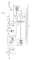
ここで図5は、スイッチングレギュレータとシリーズレギュレータとを直列接続してなる電源回路を、これら保護機能付きのレギュレートICを用いて構成した場合の一例を示す回路図である。
【0009】
図5に示すように、電源回路101は、コイルL1及びコンデンサC1にて構成された周知のローパスフィルタからなり、外部電源からの電源供給ラインに重畳された高周波のノイズ成分を除去する入力フィルタ2と、入力フィルタ2の出力を降圧して一定電圧の中間出力を生成するスイッチングレギュレータ30と、スイッチングレギュレータ30の出力(中間出力)を降圧して一定電圧の供給出力(電源回路101の出力)を生成するシリーズレギュレータ40とからなる。
【0010】
そして、スイッチングレギュレータ30は、入力フィルタ2を介してスイッチングレギュレータ30に流れ込む電流の大きさを検出するための電流検出用抵抗3と、電流検出用抵抗3が挿入された電源経路にシリーズ接続されたMOS型電界効果トランジスタ(以下単に「FET」という。)4と、FET4の出力を平滑化する平滑回路5と、平滑回路5の出力(即ち中間出力)が一定電圧となるようにFET4のゲート電圧をオンオフ制御するレギュレートIC31とからなる。
【0011】
一方、シリーズレギュレータ40は、スイッチングレギュレータ30を介してシリーズレギュレータ40に流れ込む電流の大きさを検出するための電流検出用抵抗6と、電流検出用抵抗6が挿入された電源経路にシリーズ接続されたバイポーラトランジスタ(以下単に「トランジスタ」という。)7と、トランジスタ7の出力(即ち供給出力)が一定電圧となるようにトランジスタ7のベース電流を増減制御するレギュレートIC41とからなる。
【0012】
このうち平滑回路5は、コイルC2及びコンデンサL2からなるローパスフィルタと、FET4のオフ時に導通して還流電流を流すことで、FET4のオン時にコイルL2及びコンデンサC2に蓄積された電磁エネルギーを放出させるフライホイールダイオードDとからなる周知のものである。
【0013】
また、スイッチングレギュレータ30を構成するレギュレートIC31は、平滑回路5の出力電圧を分圧する分圧回路32と、演算増幅器からなり、電流検出用抵抗3の両端電圧から電流検出用抵抗3を流れる電流の大きさを検出する電流検出回路33と、分圧回路34a及びコンパレータ34bからなり、スイッチングレギュレータ30の入力電圧を分圧した分圧値を、予め設定された参照電位(電圧しきい値)Vref1と比較することで過電圧であるか否かを判定する過電圧判定回路34と、分圧回路32により分圧されたフィードバック電圧が一定電圧となるように、FET4のゲート電圧のオンオフ比(デューティ比)を制御すると共に、電流検出回路33での検出結果から過電流が検出されるか、過電圧判定回路34にて過電圧であると判定されると、FET4がオフするようにゲート電圧を制御するスイッチング制御回路35とからなる。
【0014】
一方、シリーズレギュレータ40を構成するレギュレートIC41は、演算増幅器からなり、電流検出用抵抗6の両端電圧から電流検出用抵抗6を流れる電流の大きさを検出する電流検出回路43と、分圧回路44a及びコンパレータ44bからなり、シリーズレギュレータ40の入力電圧を分圧した分圧値を、予め設定された参照電位(電圧しきい値)Vref2と比較することで過電圧であるか否かを判定する過電圧判定回路44と、トランジスタ7の出力が一定電圧になるように、トランジスタ7のベース電流を増減することでトランジスタ7の駆動力を制御すると共に、電流検出回路43での検出結果から過電流が検出されるか、過電圧判定回路44にて過電圧であると判定されると、トランジスタ7がオフするようにベース電流を制御するシリーズ制御回路45とからなる。
【0015】
【特許文献1】
特開平9−37545号公報(段落[0002]〜[0004]、図2,図3)
【0016】
【特許文献2】
特開平6−335238号公報(段落[0004]〜[0006]、図3)
【0017】
【発明が解決しようとする課題】
ところで、このように構成された電源回路101では、電源出力ラインの地絡や短絡等により、シリーズレギュレータ40に過大な電流が流れると、必然的に、スイッチングレギュレータ30にも過大な電流が流れ、また、電源入力ラインに過大な電圧が印加されると、スイッチングレギュレータ30の入力電圧が過大となるだけでなく、その出力電圧、即ちシリーズレギュレータ40の入力電圧も、一時的に上昇する。
【0018】
つまり、両レギュレートIC31,41の電流検出回路33,34、及び過電圧判定回路34,44は、結局、同様な状態を検出することになり、これらの検出結果や判定結果に基づいて作動する保護機能は、いずれも重複したものとなる。そして、実際の動作では、過電圧及び過電流に対する各保護機能は、それぞれ、作動条件がより低く設定されたいずれか一方のレギュレートICでのみ作動することになる。
【0019】
このため、作動しない側の回路が全く無駄であるだけでなく、別々に構成された二つのレギュレートIC31,41を使用することにより、電源回路の規模、ひいてはこの電源回路101を搭載する装置の規模が大きくなってしまうという問題があった。
【0020】
また、車載電子制御装置の電源回路に電源供給を行う外部電源(例えば、ジェネレータ)には、多くの電磁負荷が接続されており、これら電磁負荷の作動時にパルス状の過大電圧(以下「サージパルス」という。)が電源回路への電源入力ラインに重畳される。
【0021】
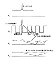
このサージパルスに対してスイッチングレギュレータ30の過電圧に対する保護機能が作動してFET4がオフされると、図6に実線にて示すように、スイッチングレギュレータ30の出力電圧V3、ひいては電源回路101の出力電圧V4が一時的に低下することになる。つまり、サージパルスが発生するたびに保護機能が作動すると、出力電圧V4の低下が頻繁に発生し、車載電子制御装置の動作が不安定になるという問題があった。但し、図中のV1は電源回路101への入力電圧、V2はFET4の出力電圧、V3は平滑回路5(スイッチングレギュレータ30)の出力電圧、V4はトランジスタ7(シリーズレギュレータ40)の出力電圧である。
【0022】
なお、電源回路101には入力フィルタ2が設けられているが、この入力フィルタ2は、サージパルスと比較して高周波のノイズを除去するのに適した特性に設定されるため、サージパルスを十分に除去することができないのである。
これに対して、図5に点線にて示すように、過電圧判定回路34への入力部分に、入力フィルタ2とは別のサージ吸収用フィルタFを設ければ、図6に点線にて示すように、サージパルスによって保護機能が作動することを防止でき、電源回路101の出力電圧V4を一定に保持することができる。しかし、この場合、電源回路101の回路規模を増大させてしまうという問題があった。
【0023】
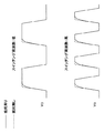
更に、スイッチングレギュレータ30のFET4の入力側に挿入された電流検出用抵抗3は、その抵抗自体が電力損失を生じさせるだけでなく、図7に実線にて示すように、FET4の出力波形(電圧波形)を鈍らせてしまい、スイッチングレギュレータ30の変換効率を低下させてしまうという問題があった。
【0024】
また、シリーズレギュレータ40での電力損失を低減するには、その入力電圧と出力電圧との差を小さくできるように、スイッチングレギュレータ30の出力電圧のリップルをできるだけ小さくすることが望ましく、そのためにはFET4のスイッチング周波数をより高くすることが効果的である。しかし、このスイッチング周波数を高くすると、電流検出用抵抗3に基づく波形鈍りの影響が相対的に大きくなり、結局、シリーズレギュレータ40での損失が低減されても、スイッチングレギュレータ30での変換効率が低下し、電源回路101全体としては、スイッチング周波数を高くした効果を十分に得ることができないという問題もあった。
【0025】
本発明は、上記問題点を解決するために、スイッチングレギュレータ及びシリーズレギュレータを直列接続した電源回路の構成を、過電圧及び過電流に対する保護機能を低下させることなく簡素化でき、しかも変換効率を向上させることが可能な電源コントローラを提供することを目的とする。
【0026】
【課題を解決するための手段】
上記目的を達成するためになされた本発明の電源コントローラでは、第1のトランジスタ及び平滑回路と共にスイッチングレギュレータを構成する第1制御回路が、第1のトランジスタを断続制御することで、外部電源からの入力を降圧して中間出力を生成し、第2のトランジスタと共にシリーズレギュレータを構成する第2制御回路が、第2のトランジスタの駆動力を増減制御することで、中間出力を降圧して供給出力を生成する。
【0027】
そして、中間出力の電圧値を検出する電圧検出回路、及びシリーズレギュレータへの入力電流または中間出力からの出力電流の電流値を検出する電流検出回路での検出結果に基づいて、第1制御回路は、少なくとも、電源回路の入力側で発生する過電圧に対する保護動作として、予め設定された電圧しきい値を超える電圧値が電圧検出回路にて検出されると第1のトランジスタをオフし、第2制御回路は、少なくとも、電源回路の出力側で発生する過電流に対する保護動作として、予め設定された電流しきい値を超える電流値が電流検出回路にて検出されると第2のトランジスタに流れる電流を制限する。
【0028】
つまり、本発明の電源コントローラを用いて構成された電源回路では、外部電源を受けてから所望の供給出力を出力するまでの一経路上に、過電圧及び過電流を検出するための構成が、重複することなく、それぞれ一つずつ設置されることになる。
【0029】
従って、本発明の電源コントローラによれば、最小限の簡素な回路構成によって、車載電子制御装置に必要とされる保護機能を備え、しかも低損失で高精度な電源回路を構成することができる。
また、本発明の電源コントローラでは、スイッチングレギュレータを構成する第1のトランジスタの入力側に、電流検出用抵抗を設ける必要がないため、第1のトランジスタの出力波形を鈍らせてしまうことがなく、スイッチングレギュレータでの変換効率を向上させることができる。しかも、シリーズレギュレータでの電力損失を低減するために、スイッチング周波数を高くした場合でも、スイッチングレギュレータでの変換効率が大きく低下することがなく、スイッチング周波数を高めることによって得られる効果を最大限に引き出すことができる。
【0030】
更に、本発明の電源コントローラでは、電圧検出回路が、中間出力、即ち平滑回路の出力に基づいて過電圧の検出を行っており、外部電源からの入力に重畳されたサージは平滑回路で吸収されるため、過電圧に対する保護動作がサージによって作動してしまうことを防止できる。つまり、本発明の電源コントローラを用いて構成される電源回路によれば、サージパルスが頻発する環境であっても、サージパルス吸収用のフィルタを別途設けることなく、安定した電圧にて電源供給を行うことができる。但し、第1のトランジスタは、サージに耐え得る程度に高耐圧のものを採用する必要がある。
【0031】
また、本発明の電源コントローラでは、過電圧の検出時に、第1制御回路が第1のトランジスタをオフするように構成されているため、平滑回路を構成するコンデンサへの過電圧の印加が抑制され、このコンデンサを、比較的低耐圧のものとすることができ、電源回路の小型化及び低コスト化を図ることができる。
【0032】
更に、本発明の電源コントローラでは、過電流の検出時に、第2の制御回路が第2のトランジスタに流れる電流を制限するように構成されているため、第2のトランジスタを流れる過電流を速やかに遮断又は制限することができる。即ち、第1のトランジスタをオフした後でも、平滑回路は蓄積されたエネルギーを第2のトランジスタに対して供給し続けようとするが、第2トランジスタをオフすることで、平滑回路に蓄積されたエネルギーが放出されるまで待つことなく、異常事態(過電圧,過電流)を速やかに収束させることができるのである。
【0033】
なお、第2制御回路は、電源回路の入力側で発生する過電圧に対する保護動作として、予め設定された電圧しきい値を超える電圧値が電圧検出回路にて検出された場合にも、第2のトランジスタをオフするように構成してもよい。この場合、過電圧の検出時には、供給出力の電圧が過大になることを確実に防止することができる。
【0034】
また、第1制御回路は、電源回路の出力側で発生する過電流に対する保護動作として、予め設定された電流しきい値を超える電流値が前記電流検出回路にて検出されると第1のトランジスタをオフするように構成してもよい。
【0035】
ところで、電圧検出回路は、中間出力の電圧をそのまま検出するのではなく、これを分圧したものを検出するのが一般的である。また、第1制御回路でも、中間出力を一定電圧に保持するためのフィードバック電圧として、中間出力の電圧をそのまま用いるのではなく、これを分圧したものを用いるのが一般的である。
【0036】
このため、電圧検出回路が分圧回路を備えている場合には、この分圧回路が生成する電圧信号を、中間出力(スイッチングレギュレータの出力)を一定電圧に保持するためのフィードバック電圧として、第1制御回路にも供給するように構成してもよい。
【0037】
この場合、電圧検出用とフィードバック電圧生成用とで、一つの分圧回路が共用されるため、電源コントローラの構成をより簡素化できる。
また、本発明の電源コントローラは、温度検出回路にて第1のトランジスタの温度を検出し、その検出結果から第1のトランジスタの過熱が検出されると、電源回路に対する保護動作を、第1及び第2制御回路のうち少なくとも一方が行うように構成してもよい。
【0038】
この場合、電流しきい値を超えない(即ち過電流と判定されない)程度の比較的大きな電流が流れるハーフショートの状態が長時間継続すると、電源回路を構成する各素子が過熱して破壊に至るおそれがあるが、このような事態を防止することができる。
【0039】
なお、予め設定された温度しきい値を超える温度(即ち過熱)が前記温度検出回路にて検出された場合には、これに対する保護動作として、第1制御回路が第1のトランジスタをオフするように構成してもよいし、第2制御回路が第2のトランジスタに流れる電流を制限する(第2のトランジスタをオフする場合を含む)ように構成してもよいし、その両方を同時に行うように構成してもよい。
【0040】
特に、異常(ハーフショート)状態が解消された時に、供給出力の電圧が正常な大きさに復帰するまでの応答性を良くする必要がある場合には、第2制御回路が第2のトランジスタをオフするように構成することが望ましく、そのような状態復帰を優先しない場合には、第1制御回路が第1のトランジスタをオフするように構成することが望ましい。
【0041】
また、温度検出手段により第1のトランジスタの過熱が検出された場合、第1制御回路や第2制御回路に第1や第2のトランジスタをオフさせる代わりに、これらとは別に設けた遮断手段が、第1のトランジスタを遮断するように構成してもよい。
【0042】
この遮断手段は、例えば、第1のトランジスタの制御端子(FETであればゲート、バイポーラトランジスタであればベース)を、第1のトランジスタがオフするようなレベルに強制的に設定するよう構成すればよい。
ところで、温度検出回路は、例えば、第1のトランジスタの近傍に配置されたダイオードの順電圧の変化から、第1のトランジスタの温度を検出するように構成することができる。
【0043】
この場合、温度検出用のダイオードは、第1のトランジスタと同一パッケージに設けられていることが望ましく、特に両者を同一の半導体基板上に形成する場合には、可能な限り近接した位置に配置することが望ましい。
次に、本発明の電源コントローラは、第2制御回路を複数備えていてもよい。このような電源コントローラは、シリーズレギュレータを複数備えた多出力の電源回路を構成する際に、好適に用いることができる。
【0044】
また、この場合、電流検出回路を一つだけ設け、スイッチングレギュレータから出力される電流の値、或いは全てのシリーズレギュレータに流入する電流の合計値を検出するように構成してもよいし、電流検出回路をシリーズレギュレータ毎に設け、各シリーズレギュレータ毎に流入する電流を検出するように構成してもよいし、ハーフショートなどの異常発生が無い或いはショートしても別途設けられた抵抗などによって他のシリーズレギュレータの動作に影響を与えない程度にその電流が十分に低く抑えられるなどの処置がなされる様な回路へ供給する為のシリーズレギュレータについては省略しても良い。
【0045】
前者の場合、構成を簡素化でき、一方、後者の場合、各レギュレータがいずれも許容範囲内の比較的大きな電流を流している時に、これを過電流として誤検出したり、いずれか一つで過電流が流れ、他が電流を流していないような時に、これを過電流として検出できなかったりすることを防止できる。
【0046】
ところで、第1のトランジスタには、MOS型電界効果トランジスタを用いることが好ましく、この場合、第1制御回路は、第1のトランジスタのゲート電圧のオンオフ比を制御するように構成すればよい。即ち、MOS型電界効果トランジスタは、オン抵抗が小さく高速動作も可能なため、スイッチングレギュレータの性能を最大限に引き出すことができる。
【0047】
一方、第2のトランジスタには、バイポーラトランジスタを用いることが好ましく、この場合、第2制御回路は、前記第2のトランジスタのベース電流の大きさを制御するように構成すればよい。即ち、バイポーラトランジスタは、ベース電流を制御することにより、コレクタ,エミッタ間の細かく制御でき、精度の高い出力電圧を得ることができるため、シリーズレギュレータの性能を最大限に引き出すことができる。
【0048】
但し、第1のトランジスタとしてMOS型電界効果トランジスタ以外のトランジスタ(例えばバイポーラトランジスタ等)を用いたり、逆に、第2のトランジスタとしてバイポーラトランジスタ以外のトランジスタ(例えばMOS型電界効果トランジスタ等)を用いたりしてもよいことは、言うまでもない。
【0049】
そして、本発明の電源コントローラは、1チップの半導体集積回路として構成してもよい。
この場合、その半導体集積回路には、第1及び第2のトランジスタのうちいずれか一方又は両方が、一体に集積されていてもよい。特に、第1のトランジスタを一体に集積する場合には、上述の温度検出用のダイオードも一体に集積することが望ましい。
【0050】
【発明の実施の形態】
以下に本発明の実施形態を図面と共に説明する。
図1は、実施形態の前提となる参考例の電源回路の構成を示す回路図、図2は、この電源回路を搭載する車載電子制御装置の概略構成図である。
【0051】
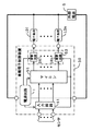
図2に示すように、車載電子制御装置50は、フィルタやA/D変換器などで構成され、装置外部に設置された各種センサ(図示せず)からの検出信号等を入力するための入力回路51と、外部電源Gから電源供給を受けて動作する電子負荷LD1〜LDnを駆動制御する駆動回路53(DR1〜DRn)と、入力回路51を介して入力された検出信号に基づいて各種演算処理を実行し、駆動回路53を動作させるための指令値(制御値)を求めるマイクロコンピュータ(マイコン)55と、外部電源Gからの電源供給を受けて装置内部の各部51〜55に所望電圧にて電源供給を行う電源回路1とを備える。
【0052】
なお、外部電源Gは、電源電圧が高く(本参考例では12V)、しかも比較的大きな電圧変動があるため、これを降圧して電圧変動のない安定した一定電圧(本実施形態では5V)での電源供給を行うために、電源回路1は設けられている。
【0053】
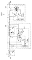
図1に示すように、電源回路1は、コイルL1及びコンデンサC1にて構成された周知のローパスフィルタからなり、外部電源からの電源供給ラインに重畳された高周波のノイズ成分を除去する入力フィルタ2と、入力フィルタ2が接続された電源経路にシリーズ接続されたMOS型電界効果トランジスタ(以下単に「FET」という。)4と、FET4の出力(電圧値V2)を平滑化して中間出力を生成する平滑回路5と、平滑回路5が生成する中間出力の電圧値V3を分圧する分圧回路11と、FET4及び平滑回路5と共にスイッチングレギュレータを構成し、分圧回路11が分圧した電圧値をフィードバック電圧として、このフィードバック電圧が予め設定された一定電圧となるように、FET4のゲート電圧をオンオフ制御するスイッチング制御回路14とを備える。
【0054】
また、電源回路1は、上記スイッチングレギュレータを介して供給される電流の大きさを検出するための電流検出用抵抗6と、電流検出用抵抗6が挿入された電源経路にシリーズ接続されたバイポーラトランジスタ7と、トランジスタ7と共にシリーズレギュレータを構成し、トランジスタ7の出力が一定電圧となるようにトランジスタ7のベース電流を増減制御するシリーズ制御回路15と、FET4の温度を検出する温度検出回路8と、演算増幅器からなり、電流検出用抵抗6の両端電圧から電流検出用抵抗6を流れる電流I1の大きさを検出する電流検出回路12と、コンパレータからなり、分圧回路11での分圧値を、予め設定された参照電位(電圧しきい値)Vref と比較することで、過電圧であるか否かを判定する過電圧判定回路13とを備える。
【0055】
このうち平滑回路5は、コイルC2及びコンデンサL2からなるローパスフィルタと、FET4のオフ時に導通して還流電流を流すことで、FET4のオン時にコイルL2及びコンデンサC2に蓄積された電磁エネルギーを放出させるフライホイールダイオードDとからなる周知のものである。
【0056】
また、温度検出回路8は、FET4に隣接して配置され、周囲温度に応じて順電圧が変化するダイオードと、ダイオードに一定電流を流す定電流回路とからなり、ダイオードの両端電圧(順電圧)からFET4の温度を検出するように構成されている。
【0057】
なお、スイッチング制御回路14は、分圧回路11から供給されるフィードバック電圧に従ってFET4のゲート電圧のオンオフ比(デューティ比)を制御するだけでなく、温度検出回路8での検出結果からFET4が過熱している(即ち予め設定された温度しきい値に対応する電圧値より大きい)ことが検出されると、FET4がオフするようゲート電圧を制御するように構成されている。
【0058】
また、シリーズ制御回路15は、トランジスタ7の出力が一定電圧になるように、トランジスタ7のベース電流を増減することでトランジスタ7の駆動力を制御するだけでなく、電流検出回路12での検出結果から過電流が流れている(即ち予め設定された電流しきい値に対応する電圧値より大きい)ことが検出されると、トランジスタ7に流れる電流が制限されるようにベース電流を絞り、また、過電圧判定回路13にて過電圧であると判定されると、トランジスタ7がオフするようベース電流を制御するように構成されている。
【0059】
そして、本参考例では、FET4,温度検出回路8,分圧回路11,電流検出回路12,過電圧判定回路13,スイッチング制御回路14,シリーズ制御回路15が単一の半導体基板上に形成され、1チップのレギュレートIC10として構成されている。
【0061】
このように構成された電源回路1では、入力フィルタ2にて高周波ノイズが除去された外部電源からの入力を、FET4,平滑回路5,スイッチング制御回路14が構成するスイッチングレギュレータが降圧して中間出力(電圧V3)を生成し、その中間出力を、トランジスタ7,シリーズ制御回路15が構成するシリーズレギュレータが降圧して供給出力(電圧V4)を生成する。
【0062】
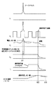
そして、図3に示すように、電源回路1の電源出力ラインのショートや、電源出力ラインから電源供給を受けるセンサや各種回路の故障などにより、電源出力ラインに電流しきい値に達する過大な電流が流れた場合(時刻t1)には、これを電流検出用抵抗6,電流検出回路12を介して検出したシリーズ制御回路15が、ベース電流を絞り込むことにより、トランジスタ7に流れ込む電流I1、ひいては電源出力ラインに流れ出す電流の大きさを制限する。つまり、過電流に対する保護機能を作動させ、電源回路1全体を保護する。このとき、トランジスタ7の出力電圧(即ち電源回路1の出力電圧)V4は、ベース電流の絞り込みと短絡により、所望の一定電圧を維持できず、この一定電圧より低下した状態となる。
【0063】
その後、過電流の原因が除去される等して、トランジスタ7に流れ込む電流I1が通常の大きさに戻ると、これを電流検出用抵抗6,電流検出回路12を介して検出したシリーズ制御回路15は、過電流に対する保護機能の作動(ベース電流の絞り込み)を解除し、供給出力が一定電圧となるようにベース電流を増減制御する通常の制御を再開する(時刻t2)。
【0064】
また、図4に示すように、電源回路1の電源入力ラインを介して過大な電圧が印加され、これに伴ってスイッチングレギュレータの出力電圧V3が上昇し、過電圧判定回路13にて過電圧であると判定されると、シリーズ制御回路15は、ベース電流を遮断してトランジスタ7をオフする。つまり、過電圧に対する保護機能を作動させ、電源出力ラインへの過大電圧の侵入を阻止して、電源出力ラインに接続されたセンサや各種回路を保護する。
【0065】
その後、スイッチング制御回路14が、その過大電圧に対応したゲート電圧の制御を行うことにより、スイッチングレギュレータの出力電圧V3が、参照電位(電圧しきい値)Vref より低く設定された復帰用参照電位まで低下すると、シリーズ制御回路15は、過電圧に対する保護機能の作動(ベース電流の遮断)を解除し、供給出力が一定電圧となるようにベース電流を増減制御する通常の制御を再開する。但し、スイッチングレギュレータの出力電圧V3が復帰用参照電位まで低下したか否かの判断は、例えば、過電圧判定回路13を構成するコンパレータにヒステリシスを持たせることで判定してもよいし、出力電圧V3が復帰用参照電位まで低下するのに十分な一定時間を設定し、その一定時間が経過したか否かにより判定してもよい。
【0066】
なお、電源入力ラインから電源回路1に侵入するサージパルスは、このサージパルスより高周波のノイズを除去するのに適した特性を有するように設定された入力フィルタ2及びFET4を通過し、平滑回路5にて平滑化される。このため、サージパルスに対しては、図4に示すように、平滑回路5のフィルタ能力を超える大きな電力を有している場合にのみ、上述した過電圧に対する保護機能が作動する(時刻t11)。
【0067】
また、電源出力ラインに接続されたセンサでの異常消費などにより、過電流と判定される大きさには達しない程度の大きな電流が流れ続けるハーフショートの状態となると、FET4の温度が上昇する。そして、FET4の温度が正常動作時に想定される上限温度(過熱判定しきい値)を超え、これを温度検出回路8を介して検出したスイッチング制御回路14は、ゲート電圧のスイッチングを停止してFET4をオフする。つまり、ハーフショートに対する保護機能を作動させ、電源回路1全体を保護する(時刻t12)。
【0068】
その後、FET4の温度が過熱判定しきい値より十分に低い復帰判定しきい値にまで低下するか、又はFET4の温度が復帰判定しきい値程度まで降下するのに必要な一定時間だけ待機した後、ハーフショート状態に対する保護機能の作動を解除して、中間出力が一定電圧となるようにゲート電圧をオンオフ制御する通常の制御を再開する(時刻t13)。
【0069】
以上説明したように、本参考例の電源回路1では、過電圧及び過電流を検出するための構成が、重複することなく、それぞれ一つずつ設置されている。
また、スイッチングレギュレータを構成するFET4の入力側に、電流検出用抵抗を設ける必要がないため、FET4の出力波形を鈍らせてしまうことがなく、スイッチングレギュレータにて優れた変換効率が得られ、しかも、シリーズレギュレータでの電力損失を低減するために、スイッチング周波数を高くした場合でも、スイッチングレギュレータでの変換効率が大きく低下することがない。
【0070】
つまり、本参考例の電源回路1は、必要最小限の簡素な回路構成であるにも関わらず、車載電子制御装置に必要とされる保護機能を備え、しかも低損失で電圧精度の優れた出力を得ることができる。
また、本参考例の電源回路1では、過電圧判定回路13が平滑回路5の出力電圧V3に基づいて過電圧の判定を行っており、外部電源Gからの入力に重畳されたサージパルスを平滑回路5で吸収させることで、過電圧に対する保護動作がサージパルスによって作動してしまうことを防止している。
【0071】
つまり、本参考例の電源回路1によれば、サージパルスが頻発する環境であっても、サージパルス吸収用のフィルタを別途設けることなく、安定した電圧にて電源供給を行うことができる。
また本参考例では、スイッチング制御回路14で使用するフィードバック電圧の生成と、過電圧判定回路13にて参照電位Vref と比較する電圧値の生成とで、分圧回路11を共用しているため回路規模や部品点数を削減できる。
【0072】
次に、本発明の実施形態について説明する。
上記参考例では、電流検出回路12での検出結果、及び過電圧判定回路13での判定結果をシリーズ制御回路15に入力して、過電圧や過電流が検出された時にはトランジスタ7をオフしたり、トランジスタ7に流れる電流を制限するように構成したが、本実施形態では、図1中に点線で示すように(判定結果については図示せず)、これらの検出結果や判定結果をスイッチング制御回路14にも入力して、FET4をオフするように構成されている。
なお、本実施形態において、レギュレートIC10が電源コントローラ、FET4が第1のトランジスタ、トランジスタ7が第2のトランジスタ、分圧回路11が電圧検出回路、スイッチング制御回路14が第1制御回路、シリーズ制御回路が第2制御回路に相当する。
このように構成された本実施形態の電源回路によれば、上記参考例と同様の効果が得られるだけでなく、過電圧の検出時に、スイッチング制御回路14が第1のトランジスタ14をオフするように構成されているため、平滑回路5を構成するコンデンサC2への過電圧の印加が抑制され、このコンデンサC2を、比較的低耐圧のものとすることができ、電源回路の小型化及び低コスト化を図ることができる。
【0073】
以上、本発明の一実施形態について説明したが、本発明は上記実施形態に限定されるものではなく、様々な態様にて実施することが可能である。
例えば、上記実施形態では、温度検出回路8での検出結果をスイッチング制御回路14に入力して、ハーフショート状態が検出された時にはFET4をオフするように構成されているが、図1中に点線で示すように、この検出結果をシリーズ制御回路15に入力して、トランジスタ7をオフしたり、トランジスタ7に流れる電流を制限したりするように構成してもよい。
【0074】
また、温度検出回路8に、温度検出用のダイオードの両端電圧が、過熱状態に相当する電圧に達したか否かを判定する過熱判定回路を内蔵させ、その判定結果をスイッチング制御回路14やシリーズ制御回路15に供給するように構成してもよい。また、このように過熱判定回路を内蔵する場合には、その判定結果をスイッチング制御回路14やシリーズ制御回路15には供給せず、過熱判定回路の出力にて、FET4のゲート電圧を直接制御して、FET4をオフするように構成してもよい。なお、この場合の過熱判定回路が、本発明における遮断手段に相当する。
【0075】
また、上記実施形態では、FET4及び温度検出回路8がレギュレートIC10に内蔵されているが、これらのうちいずれか一方、又は両方をレギュレートIC10とは別体にして構成してもよい。特に、両者をレギュレートIC10とは別体に構成した場合、図1にて点線で囲んだように、その部分は、温度検出機能付きのFET20を用いて構成してもよい。
【0076】
また、レギュレートIC10には、FET4の代わりに、又はFET4と共にバイポーラトランジスタ7を内蔵しても良く、レギュレートIC10に用いるプロセスに応じたトランジスタを一体に構成すればよい。
また、上記実施形態では、スイッチングレギュレータの出力を受けて動作するシリーズレギュレータを一つだけ設けたが、同様のシリーズレギュレータを並列に複数設けてもよい。
【0077】
この場合、レギュレートIC10は、シリーズ制御回路15のみを複数設け、電流検出回路12,過電圧判定回路13は各シリーズ制御回路15にて共通に使用されるように構成してもよいし、シリーズ制御回路15と共に電流検出回路12も複数設け、過電圧判定回路13のみが各シリーズ制御回路15にて共通に使用されるように構成してもよい。
【0078】
そして、前者の場合には、電流検出用抵抗6の出力側で電源経路を分岐し、分岐した電源経路のそれぞれにシリーズ制御回路15に対応したトランジスタ7を設ければよく、後者の場合には、平滑回路5の出力側で電源経路を分岐し、分岐した電源経路のそれぞれに電流検出回路12に対応した電流検出用抵抗6とシリーズ制御回路15に対応したトランジスタ7を設ければよい。
【図面の簡単な説明】
【図1】 実施形態の前提となる参考例の電源回路の構成を示す回路図である。
【図2】 電源回路を搭載する車載電子制御装置の概略構成図である。
【図3】 過電流に対する保護動作を説明するための波形図である。
【図4】 過電圧及びハーフショートに対する保護操作を説明するための波形図である。
【図5】 従来の電源回路の構成を示す回路図である。
【図6】 従来の電源回路における問題点を説明するための波形図である。
【図7】 従来の電源回路における問題点を説明するための波形図である。
【符号の説明】
1,101…電源回路、2…入力フィルタ、3,6…電流検出用抵抗、4…MOS型電界効果トランジスタ(FET)、5…平滑回路、7…バイポーラトランジスタ、8…温度検出回路、10,31,41…レギュレートIC、11…分圧回路、12…電流検出回路、13…過電圧判定回路、14,35…スイッチング制御回路、15,45…シリーズ制御回路、30…スイッチングレギュレータ、32…分圧回路、33,43…電流検出回路、34,44…過電圧判定回路、40…シリーズレギュレータ、50…車載電子制御装置、51…入力回路、53(DR1〜DRn)…駆動回路、G…外部電源、LD1〜LDn…電子負荷。[0001]
BACKGROUND OF THE INVENTION
The present invention relates to a power supply controller used in a power supply circuit for an in-vehicle electronic control device constituted by a switching regulator and a series regulator.
[0002]
[Prior art]
Conventionally, switching regulators and series regulators are known as power supply circuits that step down an input from an external power supply and supply power at a desired stable constant voltage (see, for example, Patent Document 1).
[0003]
Of these, the switching regulator switches the transistors connected in series to the power supply path and controls to supply only the necessary power to the smoothing circuit to obtain a constant voltage. Power loss is small although it is inferior.
[0004]
On the other hand, the series regulator is designed to obtain a constant voltage by finely controlling the voltage across the transistor by increasing / decreasing the driving force of the transistor connected in series to the power supply path, and unnecessary power is consumed by the transistor. In contrast to a switching regulator, power loss is large but output voltage accuracy is excellent because it is converted to heat.
[0005]
Therefore, these switching regulators and series regulators are connected in series, and the switching regulator steps down the output of the external power supply having a voltage higher than the desired voltage to an intermediate voltage close to the desired voltage with a small power loss. A power supply circuit configured to accurately step down the intermediate voltage to a desired voltage has been proposed (see, for example, Patent Document 2). In the power supply circuit configured as described above, the series regulator does not lose power more than necessary, and an output with excellent voltage accuracy can be obtained with small power loss.
[0006]
By the way, in a power supply circuit used in an electronic control device (hereinafter referred to as an “on-vehicle electronic control device”) mounted on an automobile, unlike a consumer product, voltage fluctuation of an external power supply that supplies power to the power supply circuit. In addition, a protection function for ensuring safety against an external abnormality factor such as a short circuit or a ground fault due to a failure of a sensor that receives power supply from a power supply circuit or various circuits or the like is essential.
[0007]
Specifically, the overvoltage applied to the power supply line on the input side of the power supply circuit (hereinafter referred to as “power supply input line”) is the voltage of the power supply line on the output side of the power supply circuit (hereinafter referred to as “power supply output line”). Adversely affects (breaks down or deteriorates) various circuits and sensors connected to the power supply output line, and overcurrent continues to flow through the power supply output line, thereby adversely affecting each element constituting the power supply circuit ( It is necessary to configure such that the protection function works against these overvoltages and overcurrents so as not to cause destruction or deterioration.
[0008]
Note that power control ICs (hereinafter referred to as “regulation ICs”) having such a protection function are widely provided for each regulation method.
FIG. 5 is a circuit diagram showing an example in which a power supply circuit formed by connecting a switching regulator and a series regulator in series is configured using these regulated ICs with a protective function.
[0009]
As shown in FIG. 5, the
[0010]
The switching regulator 30 is connected in series to a
[0011]
On the other hand, the series regulator 40 is connected in series to a
[0012]
Of these, the
[0013]
The regulating
[0014]
On the other hand, the regulation IC 41 constituting the series regulator 40 is composed of an operational amplifier, a
[0015]
[Patent Document 1]
JP-A-9-37545 (paragraphs [0002] to [0004], FIGS. 2 and 3)
[0016]
[Patent Document 2]
JP-A-6-335238 (paragraphs [0004] to [0006], FIG. 3)
[0017]
[Problems to be solved by the invention]
By the way, in the
[0018]
That is, the
[0019]
For this reason, not only the circuit on the non-operating side is useless at all, but also by using two
[0020]
Also, many electromagnetic loads are connected to an external power source (for example, a generator) that supplies power to the power circuit of the in-vehicle electronic control device. When these electromagnetic loads are activated, a pulse-like excessive voltage (hereinafter referred to as “surge pulse”) Is superimposed on the power input line to the power circuit.
[0021]
When the protection function against the overvoltage of the switching regulator 30 is activated with respect to this surge pulse and the
[0022]
The
On the other hand, if a surge absorbing filter F different from the
[0023]
Furthermore, the current detecting
[0024]
In order to reduce the power loss in the series regulator 40, it is desirable to make the ripple of the output voltage of the switching regulator 30 as small as possible so that the difference between the input voltage and the output voltage can be reduced. It is effective to increase the switching frequency. However, when the switching frequency is increased, the influence of the waveform dullness based on the
[0025]
In order to solve the above problems, the present invention can simplify the configuration of a power supply circuit in which a switching regulator and a series regulator are connected in series without reducing the protection function against overvoltage and overcurrent, and improve the conversion efficiency. An object of the present invention is to provide a power supply controller capable of performing the above.
[0026]
[Means for Solving the Problems]
In the power supply controller of the present invention made to achieve the above object, the first control circuit that constitutes the switching regulator together with the first transistor and the smoothing circuit controls the first transistor intermittently, so that the external power supply The second control circuit, which constitutes a series regulator together with the second transistor, generates an intermediate output by stepping down the input, and steps down the intermediate output by increasing / decreasing the driving force of the second transistor to reduce the supply output. Generate.
[0027]
And based on the detection result in the voltage detection circuit that detects the voltage value of the intermediate output, and the current detection circuit that detects the current value of the input current to the series regulator or the output current from the intermediate output,The first control circuit turns off the first transistor when a voltage value exceeding a preset voltage threshold is detected by the voltage detection circuit, at least as a protection operation against an overvoltage generated on the input side of the power supply circuit. When the current detection circuit detects a current value exceeding a preset current threshold value, at least as a protection operation against an overcurrent that occurs on the output side of the power supply circuit, the second control circuit The current flowing through the transistor is limited.
[0028]
In other words, in the power supply circuit configured using the power supply controller of the present invention, the configuration for detecting overvoltage and overcurrent is duplicated on one path from receiving an external power supply to outputting a desired supply output. Without one, each one will be installed.
[0029]
Therefore, according to the power supply controller of the present invention, it is possible to configure a power supply circuit having a protection function required for an in-vehicle electronic control device and having a low loss and high accuracy with a minimum simple circuit configuration.
In the power supply controller of the present invention, since it is not necessary to provide a current detection resistor on the input side of the first transistor constituting the switching regulator, the output waveform of the first transistor is not dulled. The conversion efficiency in the switching regulator can be improved. Moreover, even if the switching frequency is increased in order to reduce the power loss in the series regulator, the conversion efficiency in the switching regulator is not greatly reduced, and the effect obtained by increasing the switching frequency is maximized. be able to.
[0030]
Furthermore, in the power supply controller of the present invention, the voltage detection circuit detects an overvoltage based on the intermediate output, that is, the output of the smoothing circuit, and the surge superimposed on the input from the external power supply is absorbed by the smoothing circuit. Therefore, it is possible to prevent the protective operation against overvoltage from being activated by a surge. That is, according to the power supply circuit configured using the power supply controller of the present invention, even in an environment where surge pulses occur frequently, power can be supplied at a stable voltage without providing a surge pulse absorbing filter separately. It can be carried out. However, the first transistor needs to have a high breakdown voltage enough to withstand a surge.
[0031]
In the power supply controller of the present invention, when the overvoltage is detected, the first control circuit is configured to turn off the first transistor, so that the application of the overvoltage to the capacitor constituting the smoothing circuit is suppressed. The capacitor can have a relatively low breakdown voltage, and the power supply circuit can be reduced in size and cost.
[0032]
Furthermore, in the power supply controller of the present invention, when the overcurrent is detected, the second control circuit is configured to limit the current flowing through the second transistor, so that the overcurrent flowing through the second transistor can be quickly reduced. Can be blocked or restricted. That is, even after the first transistor is turned off, the smoothing circuit continues to supply the stored energy to the second transistor, but by turning off the second transistor, the smoothing circuit accumulates the energy in the smoothing circuit. Abnormal situations (overvoltage, overcurrent) can be quickly converged without waiting for energy to be released.
[0033]
Note that the second control circuit performs the second operation as a protection operation against an overvoltage generated on the input side of the power supply circuit even when a voltage value exceeding a preset voltage threshold is detected by the voltage detection circuit. You may comprise so that a transistor may be turned off. In this case, it is possible to reliably prevent the supply output voltage from becoming excessive when an overvoltage is detected.
[0034]
In addition, the first control circuit, as a protection operation against an overcurrent generated on the output side of the power supply circuit, detects the first transistor when a current value exceeding a preset current threshold is detected by the current detection circuit. May be configured to be turned off.
[0035]
By the way, the voltage detection circuit does not detect the intermediate output voltage as it is, but generally detects the divided voltage. Also in the first control circuit, it is general to use a voltage obtained by dividing the voltage of the intermediate output as it is as a feedback voltage for holding the intermediate output at a constant voltage.
[0036]
Therefore, when the voltage detection circuit includes a voltage dividing circuit, the voltage signal generated by the voltage dividing circuit is used as a feedback voltage for holding the intermediate output (output of the switching regulator) at a constant voltage. One control circuit may also be supplied.
[0037]
In this case, since one voltage dividing circuit is shared for voltage detection and feedback voltage generation, the configuration of the power supply controller can be further simplified.
In the power supply controller of the present invention, the temperature detection circuit detects the temperature of the first transistor, and when overheating of the first transistor is detected from the detection result, the protection operation for the power supply circuit is You may comprise so that at least one may perform among 2nd control circuits.
[0038]
In this case, if a half-short state in which a relatively large current that does not exceed the current threshold (that is, not determined as an overcurrent) continues for a long time, each element constituting the power supply circuit is overheated and is destroyed. There is a fear, but such a situation can be prevented.
[0039]
When a temperature exceeding a preset temperature threshold (that is, overheating) is detected by the temperature detection circuit, the first control circuit turns off the first transistor as a protection operation against this. The second control circuit may be configured to limit the current flowing through the second transistor (including the case where the second transistor is turned off), or both may be performed simultaneously. You may comprise.
[0040]
In particular, when it is necessary to improve the response until the supply output voltage returns to a normal level when the abnormal (half short-circuit) state is resolved, the second control circuit turns the second transistor on. It is desirable to configure so that it is turned off. When priority is not given to such state recovery, it is desirable that the first control circuit be configured to turn off the first transistor.
[0041]
In addition, when overheating of the first transistor is detected by the temperature detection means, instead of turning off the first and second transistors in the first control circuit and the second control circuit, a separate cutoff means is provided. The first transistor may be cut off.
[0042]
For example, if the blocking means is configured to forcibly set the control terminal of the first transistor (the gate for the FET, the base for the bipolar transistor) to a level at which the first transistor is turned off. Good.
By the way, the temperature detection circuit can be configured to detect the temperature of the first transistor from, for example, a change in the forward voltage of a diode arranged in the vicinity of the first transistor.
[0043]
In this case, the temperature detection diode is preferably provided in the same package as the first transistor. In particular, when both are formed on the same semiconductor substrate, they are arranged as close as possible. It is desirable.
Next, the power supply controller of the present invention may include a plurality of second control circuits. Such a power supply controller can be preferably used when configuring a multi-output power supply circuit including a plurality of series regulators.
[0044]
In this case, only one current detection circuit may be provided to detect the value of the current output from the switching regulator or the total value of the current flowing into all the series regulators. A circuit may be provided for each series regulator, and the current flowing into each series regulator may be detected. A series regulator for supplying to a circuit where measures such as suppressing the current sufficiently low so as not to affect the operation of the series regulator may be omitted.
[0045]
In the former case, the configuration can be simplified. On the other hand, in the latter case, when each regulator is passing a relatively large current within the allowable range, this is erroneously detected as an overcurrent, or any one of them can be detected. When an overcurrent flows and no other current flows, it can be prevented that this cannot be detected as an overcurrent.
[0046]
By the way, it is preferable to use a MOS field effect transistor as the first transistor. In this case, the first control circuit may be configured to control the on / off ratio of the gate voltage of the first transistor. That is, since the MOS field effect transistor has a small on-resistance and can operate at high speed, the performance of the switching regulator can be maximized.
[0047]
On the other hand, it is preferable to use a bipolar transistor as the second transistor. In this case, the second control circuit may be configured to control the magnitude of the base current of the second transistor. That is, the bipolar transistor can be finely controlled between the collector and the emitter by controlling the base current, and a highly accurate output voltage can be obtained, so that the performance of the series regulator can be maximized.
[0048]
However, a transistor other than a MOS field effect transistor (such as a bipolar transistor) is used as the first transistor, and conversely, a transistor other than a bipolar transistor (such as a MOS field effect transistor) is used as the second transistor. Needless to say, you can.
[0049]
The power supply controller of the present invention may be configured as a one-chip semiconductor integrated circuit.
In this case, one or both of the first and second transistors may be integrated in the semiconductor integrated circuit. In particular, when the first transistors are integrated together, it is desirable to integrate the above-described temperature detection diodes together.
[0050]
DETAILED DESCRIPTION OF THE INVENTION
Embodiments of the present invention will be described below with reference to the drawings.
FIG. 1 shows an embodiment.Reference examplesFIG. 2 is a schematic configuration diagram of an in-vehicle electronic control device in which the power supply circuit is mounted.
[0051]
As shown in FIG. 2, the on-vehicle
[0052]
The external power supply G has a high power supply voltage (Reference exampleIn this embodiment, the
[0053]
As shown in FIG. 1, the
[0054]
The
[0055]
Of these, the smoothing
[0056]
The
[0057]
The switching control circuit 14 not only controls the on / off ratio (duty ratio) of the gate voltage of the
[0058]
The series control circuit 15 not only controls the driving power of the
[0059]
[0061]
In the
[0062]
As shown in FIG. 3, an excessive current that reaches the current threshold value in the power supply output line due to a short circuit of the power supply output line of the
[0063]
Thereafter, when the cause of the overcurrent is removed and the current I1 flowing into the
[0064]
Further, as shown in FIG. 4, an excessive voltage is applied via the power supply input line of the
[0065]
Thereafter, the switching control circuit 14 controls the gate voltage corresponding to the excessive voltage, so that the output voltage V3 of the switching regulator reaches the return reference potential set lower than the reference potential (voltage threshold value) Vref. When the voltage drops, the series control circuit 15 cancels the operation of the protection function against overvoltage (blocking of the base current), and resumes normal control for increasing / decreasing the base current so that the supply output becomes a constant voltage. However, the determination as to whether or not the output voltage V3 of the switching regulator has dropped to the return reference potential may be made by, for example, providing a hysteresis to the comparator that constitutes the overvoltage determination circuit 13, or the output voltage V3. May be determined by setting a certain time sufficient for the voltage to fall to the return reference potential and determining whether the certain time has elapsed.
[0066]
The surge pulse that enters the
[0067]
Further, the
[0068]
After that, after the temperature of the
[0069]
As explained above,Reference exampleIn the
In addition, since it is not necessary to provide a current detection resistor on the input side of the
[0070]
That meansReference exampleThe
Also,Reference exampleIn the
[0071]
That meansReference exampleAccording to the
AlsoReference exampleThen, since the voltage divider circuit 11 is shared between the generation of the feedback voltage used in the switching control circuit 14 and the generation of the voltage value to be compared with the reference potential Vref in the overvoltage determination circuit 13, the circuit scale and the number of parts are reduced. Can be reduced.
[0072]
Next, an embodiment of the present invention will be described.
Reference example aboveThen, the detection result in the current detection circuit 12 and the determination result in the overvoltage determination circuit 13 are input to the series control circuit 15, and when an overvoltage or overcurrent is detected, the
In this embodiment, the
According to the power supply circuit of the present embodiment configured as described above, not only the same effect as the above-described reference example is obtained, but also the switching control circuit 14 turns off the first transistor 14 when an overvoltage is detected. Therefore, application of overvoltage to the capacitor C2 constituting the smoothing
[0073]
As mentioned above, although one Embodiment of this invention was described, this invention is not limited to the said embodiment, It is possible to implement in various aspects.
For example,In the above embodiment, the detection result in the
[0074]
Further, the
[0075]
Moreover, in the said embodiment, although FET4 and the
[0076]
In addition, the
In the above embodiment, only one series regulator that operates in response to the output of the switching regulator is provided. However, a plurality of similar series regulators may be provided in parallel.
[0077]
In this case, the
[0078]
In the former case, the power supply path may be branched on the output side of the
[Brief description of the drawings]
FIG. 1 EmbodimentReference examples on which to assumeIt is a circuit diagram which shows the structure of this power supply circuit.
FIG. 2 is a schematic configuration diagram of an in-vehicle electronic control device equipped with a power supply circuit.
FIG. 3 is a waveform diagram for explaining a protection operation against an overcurrent.
FIG. 4 is a waveform diagram for explaining a protection operation against overvoltage and half short-circuit.
FIG. 5 is a circuit diagram showing a configuration of a conventional power supply circuit.
FIG. 6 is a waveform diagram for explaining problems in a conventional power supply circuit.
FIG. 7 is a waveform diagram for explaining problems in a conventional power supply circuit.
[Explanation of symbols]
DESCRIPTION OF SYMBOLS 1,101 ... Power supply circuit, 2 ... Input filter, 3, 6 ... Current detection resistor, 4 ... MOS field effect transistor (FET), 5 ... Smoothing circuit, 7 ... Bipolar transistor, 8 ... Temperature detection circuit, 10, 31, 41... Regulating IC, 11... Voltage dividing circuit, 12... Current detection circuit, 13 .. Overvoltage determination circuit, 14, 35 ... Switching control circuit, 15, 45 ... Series control circuit, 30 ... Switching regulator, 32.
Claims (15)
電源経路にシリーズ接続された第1のトランジスタ及び該第1のトランジスタの出力を平滑化する平滑回路と共に前記スイッチングレギュレータを構成し、前記中間出力が一定電圧となるように前記第1のトランジスタを断続制御する第1制御回路と、
電源経路にシリーズ接続された第2のトランジスタと共に前記シリーズレギュレータを構成し、前記供給出力が一定電圧となるように前記第2のトランジスタの駆動力を増減制御する第2制御回路と、
前記中間出力の電圧値を検出する電圧検出回路と、
前記シリーズレギュレータへの入力電流または前記中間出力からの出力電流の電流値を検出する電流検出回路と、
を備え、
前記第1制御回路は、少なくとも、前記電源回路の入力側で発生する過電圧に対する保護動作として、予め設定された電圧しきい値を超える電圧値が前記電圧検出回路にて検出されると前記第1のトランジスタをオフし、
前記第2制御回路は、少なくとも、前記電源回路の出力側で発生する過電流に対する保護動作として、予め設定された電流しきい値を超える電流値が前記電流検出回路にて検出されると前記第2のトランジスタに流れる電流を制限することを特徴とする電源コントローラ。A power supply controller for use in a power supply circuit for an in-vehicle electronic control device configured by a switching regulator that generates an intermediate output by stepping down an input from an external power source and a series regulator that generates a supply output by stepping down the intermediate output,
The switching regulator is configured together with a first transistor connected in series to the power supply path and a smoothing circuit for smoothing the output of the first transistor, and the first transistor is intermittently connected so that the intermediate output becomes a constant voltage. A first control circuit for controlling;
A second control circuit that constitutes the series regulator together with a second transistor connected in series to a power supply path, and controls increase / decrease of the driving force of the second transistor so that the supply output becomes a constant voltage;
A voltage detection circuit for detecting a voltage value of the intermediate output;
A current detection circuit for detecting a current value of an input current to the series regulator or an output current from the intermediate output;
Equipped with a,
When the voltage detection circuit detects a voltage value exceeding a preset voltage threshold as at least a protection operation against an overvoltage generated on the input side of the power supply circuit , the first control circuit detects the first control circuit . Turn off the transistor,
When the current detection circuit detects a current value exceeding a preset current threshold value as at least a protection operation against an overcurrent generated on the output side of the power supply circuit , the second control circuit performs the first control . A power supply controller that limits a current flowing through the two transistors .
該分圧回路が生成する電圧信号を、前記スイッチングレギュレータの出力を一定電圧に保持するためのフィードバック電圧として、前記第1制御回路にも供給することを特徴とする請求項1乃至請求項3いずれか記載の電源コントローラ。The voltage detection circuit includes a voltage dividing circuit that divides the output voltage of the switching regulator,
A voltage signal voltage dividing circuit is produced, as a feedback voltage to hold the output of the switching regulator to a constant voltage, any claims 1 to 3, characterized in that also supplied to the first control circuit Or the power controller described.
該温度検出回路での検出結果に基づいて、前記電源回路に対する保護動作を、前記第1及び第2制御回路のうち少なくとも一方が行うことを特徴とする請求項1乃至請求項4いずれか記載の電源コントローラ。A temperature detection circuit for detecting the temperature of the first transistor;
Based on the detection result of the temperature detection circuit, the protection operation against the power supply circuit, at least one of and performing claims 1 to 4, wherein one of said first and second control circuit Power controller.
該温度検出回路により前記第1トランジスタの過熱が検出されると、該第1トランジスタの出力を遮断する遮断手段と、
を備えることを特徴とする請求項1乃至請求項4いずれか記載の電源コントローラ。A temperature detection circuit for detecting a temperature of the first transistor;
Shut-off means for shutting off the output of the first transistor when the temperature detection circuit detects overheating of the first transistor;
It claims 1 to 4 power supply controller according to any one, characterized in that it comprises a.
前記第1制御回路は、前記第1のトランジスタのゲート電圧のオンオフ比を制御することを特徴とする請求項1乃至請求項11いずれか記載の電源コントローラ。The first transistor is a MOS field effect transistor,
Wherein the first control circuit, the first of claims 1 to 11 power supply controller according to any one and controls the on-off ratio of the gate voltage of the transistor.
前記第2制御回路は、前記第2のトランジスタのベース電流の大きさを制御することを特徴とする請求項1乃至請求項12いずれか記載の電源コントローラ。The second transistor is a bipolar transistor,
The power supply controller according to any one of claims 1 to 12, wherein the second control circuit controls a magnitude of a base current of the second transistor.
Priority Applications (2)
| Application Number | Priority Date | Filing Date | Title |
|---|---|---|---|
| JP2002307431A JP3705259B2 (en) | 2002-10-22 | 2002-10-22 | Power controller |
| US10/678,129 US7038430B2 (en) | 2002-10-22 | 2003-10-06 | Power control circuit |
Applications Claiming Priority (1)
| Application Number | Priority Date | Filing Date | Title |
|---|---|---|---|
| JP2002307431A JP3705259B2 (en) | 2002-10-22 | 2002-10-22 | Power controller |
Publications (2)
| Publication Number | Publication Date |
|---|---|
| JP2004147391A JP2004147391A (en) | 2004-05-20 |
| JP3705259B2 true JP3705259B2 (en) | 2005-10-12 |
Family
ID=32089439
Family Applications (1)
| Application Number | Title | Priority Date | Filing Date |
|---|---|---|---|
| JP2002307431A Expired - Fee Related JP3705259B2 (en) | 2002-10-22 | 2002-10-22 | Power controller |
Country Status (2)
| Country | Link |
|---|---|
| US (1) | US7038430B2 (en) |
| JP (1) | JP3705259B2 (en) |
Families Citing this family (83)
| Publication number | Priority date | Publication date | Assignee | Title |
|---|---|---|---|---|
| JP2003250228A (en) * | 2002-02-21 | 2003-09-05 | Nec Tokin Corp | Power circuit and control method therefor |
| JP4461827B2 (en) * | 2004-02-17 | 2010-05-12 | 株式会社デンソー | Power circuit |
| JP4220916B2 (en) * | 2004-02-24 | 2009-02-04 | 株式会社デンソー | Semiconductor switch |
| JP2006140587A (en) * | 2004-11-10 | 2006-06-01 | Auto Network Gijutsu Kenkyusho:Kk | Pwm signal generating circuit and pwm control circuit |
| JP2006314168A (en) * | 2005-05-09 | 2006-11-16 | Sharp Corp | Power circuit for liquid crystal display |
| US10693415B2 (en) | 2007-12-05 | 2020-06-23 | Solaredge Technologies Ltd. | Testing of a photovoltaic panel |
| US11881814B2 (en) | 2005-12-05 | 2024-01-23 | Solaredge Technologies Ltd. | Testing of a photovoltaic panel |
| US7420355B2 (en) * | 2006-07-11 | 2008-09-02 | Artesyn Technologies, Inc. | DC-DC converter with over-voltage protection |
| US11735910B2 (en) | 2006-12-06 | 2023-08-22 | Solaredge Technologies Ltd. | Distributed power system using direct current power sources |
| US8947194B2 (en) | 2009-05-26 | 2015-02-03 | Solaredge Technologies Ltd. | Theft detection and prevention in a power generation system |
| US11569659B2 (en) | 2006-12-06 | 2023-01-31 | Solaredge Technologies Ltd. | Distributed power harvesting systems using DC power sources |
| US11888387B2 (en) | 2006-12-06 | 2024-01-30 | Solaredge Technologies Ltd. | Safety mechanisms, wake up and shutdown methods in distributed power installations |
| US9130401B2 (en) | 2006-12-06 | 2015-09-08 | Solaredge Technologies Ltd. | Distributed power harvesting systems using DC power sources |
| US8963369B2 (en) | 2007-12-04 | 2015-02-24 | Solaredge Technologies Ltd. | Distributed power harvesting systems using DC power sources |
| US8319471B2 (en) | 2006-12-06 | 2012-11-27 | Solaredge, Ltd. | Battery power delivery module |
| US8319483B2 (en) | 2007-08-06 | 2012-11-27 | Solaredge Technologies Ltd. | Digital average input current control in power converter |
| US11296650B2 (en) | 2006-12-06 | 2022-04-05 | Solaredge Technologies Ltd. | System and method for protection during inverter shutdown in distributed power installations |
| US9088178B2 (en) | 2006-12-06 | 2015-07-21 | Solaredge Technologies Ltd | Distributed power harvesting systems using DC power sources |
| US8816535B2 (en) | 2007-10-10 | 2014-08-26 | Solaredge Technologies, Ltd. | System and method for protection during inverter shutdown in distributed power installations |
| US8013472B2 (en) | 2006-12-06 | 2011-09-06 | Solaredge, Ltd. | Method for distributed power harvesting using DC power sources |
| US8384243B2 (en) | 2007-12-04 | 2013-02-26 | Solaredge Technologies Ltd. | Distributed power harvesting systems using DC power sources |
| US11855231B2 (en) | 2006-12-06 | 2023-12-26 | Solaredge Technologies Ltd. | Distributed power harvesting systems using DC power sources |
| US8618692B2 (en) | 2007-12-04 | 2013-12-31 | Solaredge Technologies Ltd. | Distributed power system using direct current power sources |
| US11687112B2 (en) | 2006-12-06 | 2023-06-27 | Solaredge Technologies Ltd. | Distributed power harvesting systems using DC power sources |
| US11309832B2 (en) | 2006-12-06 | 2022-04-19 | Solaredge Technologies Ltd. | Distributed power harvesting systems using DC power sources |
| US9112379B2 (en) | 2006-12-06 | 2015-08-18 | Solaredge Technologies Ltd. | Pairing of components in a direct current distributed power generation system |
| US8473250B2 (en) | 2006-12-06 | 2013-06-25 | Solaredge, Ltd. | Monitoring of distributed power harvesting systems using DC power sources |
| US11728768B2 (en) | 2006-12-06 | 2023-08-15 | Solaredge Technologies Ltd. | Pairing of components in a direct current distributed power generation system |
| JP2008197892A (en) * | 2007-02-13 | 2008-08-28 | Sharp Corp | Series regulator |
| JP2008257525A (en) * | 2007-04-05 | 2008-10-23 | Denso Corp | Power unit |
| JP4934491B2 (en) * | 2007-05-09 | 2012-05-16 | 株式会社リコー | Overheat protection circuit, electronic device including the same, and control method thereof |
| JP4345845B2 (en) * | 2007-05-16 | 2009-10-14 | 株式会社デンソー | Power supply |
| CN101933209B (en) | 2007-12-05 | 2015-10-21 | 太阳能安吉有限公司 | Release mechanism in distributed electrical power apparatus, to wake up and method for closing |
| US9291696B2 (en) | 2007-12-05 | 2016-03-22 | Solaredge Technologies Ltd. | Photovoltaic system power tracking method |
| US8049523B2 (en) | 2007-12-05 | 2011-11-01 | Solaredge Technologies Ltd. | Current sensing on a MOSFET |
| US11264947B2 (en) | 2007-12-05 | 2022-03-01 | Solaredge Technologies Ltd. | Testing of a photovoltaic panel |
| JP4479797B2 (en) * | 2008-01-23 | 2010-06-09 | 株式会社デンソー | Electronic control unit |
| WO2009118682A2 (en) | 2008-03-24 | 2009-10-01 | Solaredge Technolgies Ltd. | Zero current switching |
| WO2009136358A1 (en) | 2008-05-05 | 2009-11-12 | Solaredge Technologies Ltd. | Direct current power combiner |
| WO2010020898A1 (en) * | 2008-08-19 | 2010-02-25 | Nxp B.V. | A surge protection circuit |
| US8710699B2 (en) | 2009-12-01 | 2014-04-29 | Solaredge Technologies Ltd. | Dual use photovoltaic system |
| US8766696B2 (en) | 2010-01-27 | 2014-07-01 | Solaredge Technologies Ltd. | Fast voltage level shifter circuit |
| TWI405396B (en) * | 2010-02-03 | 2013-08-11 | Beyond Innovation Tech Co Ltd | Boost type power converting apparatus |
| KR101152476B1 (en) * | 2010-08-19 | 2012-07-06 | 삼성에스디아이 주식회사 | charger and discharer for secondary battery |
| US10230310B2 (en) | 2016-04-05 | 2019-03-12 | Solaredge Technologies Ltd | Safety switch for photovoltaic systems |
| GB2485527B (en) | 2010-11-09 | 2012-12-19 | Solaredge Technologies Ltd | Arc detection and prevention in a power generation system |
| US10673222B2 (en) | 2010-11-09 | 2020-06-02 | Solaredge Technologies Ltd. | Arc detection and prevention in a power generation system |
| US10673229B2 (en) | 2010-11-09 | 2020-06-02 | Solaredge Technologies Ltd. | Arc detection and prevention in a power generation system |
| GB2486408A (en) | 2010-12-09 | 2012-06-20 | Solaredge Technologies Ltd | Disconnection of a string carrying direct current |
| GB2483317B (en) | 2011-01-12 | 2012-08-22 | Solaredge Technologies Ltd | Serially connected inverters |
| US8570005B2 (en) | 2011-09-12 | 2013-10-29 | Solaredge Technologies Ltd. | Direct current link circuit |
| JP5267644B2 (en) * | 2011-11-30 | 2013-08-21 | トヨタ自動車株式会社 | Power supply device, power supply method, and motor drive system |
| GB2498365A (en) | 2012-01-11 | 2013-07-17 | Solaredge Technologies Ltd | Photovoltaic module |
| GB2498791A (en) | 2012-01-30 | 2013-07-31 | Solaredge Technologies Ltd | Photovoltaic panel circuitry |
| US9853565B2 (en) | 2012-01-30 | 2017-12-26 | Solaredge Technologies Ltd. | Maximized power in a photovoltaic distributed power system |
| GB2498790A (en) | 2012-01-30 | 2013-07-31 | Solaredge Technologies Ltd | Maximising power in a photovoltaic distributed power system |
| GB2499991A (en) | 2012-03-05 | 2013-09-11 | Solaredge Technologies Ltd | DC link circuit for photovoltaic array |
| JP2013209017A (en) * | 2012-03-30 | 2013-10-10 | Toyota Industries Corp | Power circuit |
| EP3499695A1 (en) | 2012-05-25 | 2019-06-19 | Solaredge Technologies Ltd. | Circuit for interconnected direct current power sources |
| US10115841B2 (en) | 2012-06-04 | 2018-10-30 | Solaredge Technologies Ltd. | Integrated photovoltaic panel circuitry |
| FR2994750B1 (en) * | 2012-08-23 | 2015-12-11 | St Microelectronics Rousset | SUPPLYING A FLOATING POTENTIAL LOAD |
| US9941813B2 (en) | 2013-03-14 | 2018-04-10 | Solaredge Technologies Ltd. | High frequency multi-level inverter |
| US9548619B2 (en) | 2013-03-14 | 2017-01-17 | Solaredge Technologies Ltd. | Method and apparatus for storing and depleting energy |
| EP3506370B1 (en) | 2013-03-15 | 2023-12-20 | Solaredge Technologies Ltd. | Bypass mechanism |
| US9318974B2 (en) | 2014-03-26 | 2016-04-19 | Solaredge Technologies Ltd. | Multi-level inverter with flying capacitor topology |
| JP6232133B2 (en) | 2014-06-10 | 2017-11-15 | 日立オートモティブシステムズ株式会社 | Electronic control unit |
| US10177646B2 (en) * | 2014-06-13 | 2019-01-08 | City University Of Hong Kong | Power factor correction circuit for a power electronic system |
| US9698672B2 (en) * | 2014-06-16 | 2017-07-04 | City University Of Hong Kong | Input filter for a power electronic system |
| JP6460708B2 (en) * | 2014-09-30 | 2019-01-30 | コイト電工株式会社 | Power control circuit |
| US10599113B2 (en) | 2016-03-03 | 2020-03-24 | Solaredge Technologies Ltd. | Apparatus and method for determining an order of power devices in power generation systems |
| CN107153212B (en) | 2016-03-03 | 2023-07-28 | 太阳能安吉科技有限公司 | Method for mapping a power generation facility |
| US11081608B2 (en) | 2016-03-03 | 2021-08-03 | Solaredge Technologies Ltd. | Apparatus and method for determining an order of power devices in power generation systems |
| US11018623B2 (en) | 2016-04-05 | 2021-05-25 | Solaredge Technologies Ltd. | Safety switch for photovoltaic systems |
| US11177663B2 (en) | 2016-04-05 | 2021-11-16 | Solaredge Technologies Ltd. | Chain of power devices |
| CN105810163B (en) * | 2016-05-04 | 2018-08-14 | 深圳市华星光电技术有限公司 | Boost DC-direct current transducer |
| JP6686782B2 (en) * | 2016-08-08 | 2020-04-22 | トヨタ自動車株式会社 | Power system |
| JP6132997B1 (en) * | 2017-01-30 | 2017-05-24 | リオン株式会社 | Audible band signal generator and audiometer |
| JP6943650B2 (en) * | 2017-07-07 | 2021-10-06 | ローム株式会社 | High-side transistor drive circuit, DC / DC converter control circuit using it, DC / DC converter |
| WO2020066030A1 (en) * | 2018-09-28 | 2020-04-02 | 三菱電機株式会社 | Dc power supply device, motor drive device, blower, compressor and air conditioner |
| JP7332022B2 (en) | 2018-10-02 | 2023-08-23 | カシオ計算機株式会社 | Power supply circuits and electronic equipment |
| JP7063223B2 (en) * | 2018-10-05 | 2022-05-09 | 株式会社デンソー | Electronic control device |
| CN110971114B (en) * | 2019-12-19 | 2021-03-09 | 北京德亚特应用科技有限公司 | Overvoltage protection circuit and power supply equipment |
| CN111697551B (en) * | 2020-06-05 | 2022-04-01 | 茂硕电源科技股份有限公司 | Voltage protection circuit and electronic equipment |
Family Cites Families (13)
| Publication number | Priority date | Publication date | Assignee | Title |
|---|---|---|---|---|
| JPS524035A (en) * | 1975-06-28 | 1977-01-12 | Tohoku Metal Ind Ltd | Dc stabilizing power source |
| JPH03136112A (en) | 1989-10-23 | 1991-06-10 | Sharp Corp | Regulated power supply circuit |
| JPH05127765A (en) | 1991-11-01 | 1993-05-25 | Nippondenso Co Ltd | Power supply unit for on-vehicle electronic device |
| JPH05130730A (en) | 1991-11-01 | 1993-05-25 | Fuji Electric Co Ltd | Protecting circuit for dc-dc converter |
| JPH06335238A (en) | 1993-05-17 | 1994-12-02 | Mitsubishi Electric Corp | Power supply device |
| JP3489197B2 (en) | 1994-07-28 | 2004-01-19 | 日産自動車株式会社 | Constant voltage power supply circuit |
| JPH0937545A (en) | 1995-07-17 | 1997-02-07 | Mitsubishi Electric Corp | Power supply circuit |
| JP3384521B2 (en) * | 1996-06-07 | 2003-03-10 | 矢崎総業株式会社 | Switching device |
| US5808453A (en) * | 1996-08-21 | 1998-09-15 | Siliconix Incorporated | Synchronous current sharing pulse width modulator |
| JP3613927B2 (en) | 1997-04-23 | 2005-01-26 | 株式会社日本自動車部品総合研究所 | ECU power supply system for vehicle |
| JP3680978B2 (en) | 1998-11-04 | 2005-08-10 | 株式会社デンソー | In-vehicle power supply |
| JP2001268895A (en) | 2000-03-21 | 2001-09-28 | Toyota Autom Loom Works Ltd | Dc-dc converter and overvoltage detector provided therein |
| JP4651832B2 (en) | 2001-03-05 | 2011-03-16 | 富士通セミコンダクター株式会社 | Overvoltage protection device for power system |
-
2002
- 2002-10-22 JP JP2002307431A patent/JP3705259B2/en not_active Expired - Fee Related
-
2003
- 2003-10-06 US US10/678,129 patent/US7038430B2/en not_active Expired - Lifetime
Also Published As
| Publication number | Publication date |
|---|---|
| US7038430B2 (en) | 2006-05-02 |
| JP2004147391A (en) | 2004-05-20 |
| US20040075423A1 (en) | 2004-04-22 |
Similar Documents
| Publication | Publication Date | Title |
|---|---|---|
| JP3705259B2 (en) | Power controller | |
| JP4589966B2 (en) | Power supply control device and semiconductor device | |
| JP4579293B2 (en) | Power supply control device | |
| US7068485B2 (en) | Multi-output electric power source device and vehicle-mounted electronic control device | |
| KR101391657B1 (en) | semiconductor device | |
| US8054605B2 (en) | Power supply controller | |
| EP0585926B1 (en) | Insulated gate semiconductor device | |
| US6891707B2 (en) | Semiconductor protection circuit | |
| JP5430608B2 (en) | Semiconductor switching element drive circuit | |
| US7542251B2 (en) | Auto-protected power modules and methods | |
| EP2955825B1 (en) | Gate driving circuit | |
| US20050213276A1 (en) | DC regulated power supply comprising | |
| JP2003009385A (en) | Component including circuit element subjected to active control | |
| WO2007074828A1 (en) | Power supply control device and its threshold value modification method | |
| US7161783B2 (en) | Overcurrent protection circuit for switching power supply | |
| US11545970B2 (en) | Current detection circuit, current detection method, and semiconductor module | |
| JP2009213305A (en) | Power converter | |
| JP2017152923A (en) | Load drive device | |
| US6717828B2 (en) | Power semiconductor device | |
| US4555742A (en) | Short detection circuit and method for an electrical load | |
| WO2019225121A1 (en) | Protection circuit for power semiconductor element and power module | |
| WO2002037671A1 (en) | Integrated circuit with current sense circuit and associated methods | |
| US6674624B2 (en) | Dimmer | |
| JPH08196073A (en) | Power supply device | |
| KR101325184B1 (en) | Over-voltage protection circuit and semiconductor device having the over-voltage protection circuit |
Legal Events
| Date | Code | Title | Description |
|---|---|---|---|
| A977 | Report on retrieval |
Free format text: JAPANESE INTERMEDIATE CODE: A971007 Effective date: 20050328 |
|
| A131 | Notification of reasons for refusal |
Free format text: JAPANESE INTERMEDIATE CODE: A131 Effective date: 20050405 |
|
| A521 | Request for written amendment filed |
Free format text: JAPANESE INTERMEDIATE CODE: A523 Effective date: 20050606 |
|
| TRDD | Decision of grant or rejection written | ||
| A01 | Written decision to grant a patent or to grant a registration (utility model) |
Free format text: JAPANESE INTERMEDIATE CODE: A01 Effective date: 20050705 |
|
| A61 | First payment of annual fees (during grant procedure) |
Free format text: JAPANESE INTERMEDIATE CODE: A61 Effective date: 20050718 |
|
| R150 | Certificate of patent or registration of utility model |
Ref document number: 3705259 Country of ref document: JP Free format text: JAPANESE INTERMEDIATE CODE: R150 Free format text: JAPANESE INTERMEDIATE CODE: R150 |
|
| FPAY | Renewal fee payment (event date is renewal date of database) |
Free format text: PAYMENT UNTIL: 20080805 Year of fee payment: 3 |
|
| FPAY | Renewal fee payment (event date is renewal date of database) |
Free format text: PAYMENT UNTIL: 20110805 Year of fee payment: 6 |
|
| FPAY | Renewal fee payment (event date is renewal date of database) |
Free format text: PAYMENT UNTIL: 20120805 Year of fee payment: 7 |
|
| FPAY | Renewal fee payment (event date is renewal date of database) |
Free format text: PAYMENT UNTIL: 20130805 Year of fee payment: 8 |
|
| R250 | Receipt of annual fees |
Free format text: JAPANESE INTERMEDIATE CODE: R250 |
|
| R250 | Receipt of annual fees |
Free format text: JAPANESE INTERMEDIATE CODE: R250 |
|
| R250 | Receipt of annual fees |
Free format text: JAPANESE INTERMEDIATE CODE: R250 |
|
| R250 | Receipt of annual fees |
Free format text: JAPANESE INTERMEDIATE CODE: R250 |
|
| R250 | Receipt of annual fees |
Free format text: JAPANESE INTERMEDIATE CODE: R250 |
|
| R250 | Receipt of annual fees |
Free format text: JAPANESE INTERMEDIATE CODE: R250 |
|
| LAPS | Cancellation because of no payment of annual fees |