EP3098953A2 - Pre-charge circuit and photovoltaic inverter - Google Patents
Pre-charge circuit and photovoltaic inverter Download PDFInfo
- Publication number
- EP3098953A2 EP3098953A2 EP16171181.7A EP16171181A EP3098953A2 EP 3098953 A2 EP3098953 A2 EP 3098953A2 EP 16171181 A EP16171181 A EP 16171181A EP 3098953 A2 EP3098953 A2 EP 3098953A2
- Authority
- EP
- European Patent Office
- Prior art keywords
- charge circuit
- alternating current
- voltage
- charging capacitor
- photovoltaic inverter
- Prior art date
- Legal status (The legal status is an assumption and is not a legal conclusion. Google has not performed a legal analysis and makes no representation as to the accuracy of the status listed.)
- Pending
Links
Images


Classifications
-
- H—ELECTRICITY
- H02—GENERATION; CONVERSION OR DISTRIBUTION OF ELECTRIC POWER
- H02M—APPARATUS FOR CONVERSION BETWEEN AC AND AC, BETWEEN AC AND DC, OR BETWEEN DC AND DC, AND FOR USE WITH MAINS OR SIMILAR POWER SUPPLY SYSTEMS; CONVERSION OF DC OR AC INPUT POWER INTO SURGE OUTPUT POWER; CONTROL OR REGULATION THEREOF
- H02M1/00—Details of apparatus for conversion
- H02M1/36—Means for starting or stopping converters
-
- H—ELECTRICITY
- H02—GENERATION; CONVERSION OR DISTRIBUTION OF ELECTRIC POWER
- H02M—APPARATUS FOR CONVERSION BETWEEN AC AND AC, BETWEEN AC AND DC, OR BETWEEN DC AND DC, AND FOR USE WITH MAINS OR SIMILAR POWER SUPPLY SYSTEMS; CONVERSION OF DC OR AC INPUT POWER INTO SURGE OUTPUT POWER; CONTROL OR REGULATION THEREOF
- H02M7/00—Conversion of ac power input into dc power output; Conversion of dc power input into ac power output
- H02M7/02—Conversion of ac power input into dc power output without possibility of reversal
- H02M7/04—Conversion of ac power input into dc power output without possibility of reversal by static converters
- H02M7/12—Conversion of ac power input into dc power output without possibility of reversal by static converters using discharge tubes with control electrode or semiconductor devices with control electrode
- H02M7/125—Avoiding or suppressing excessive transient voltages or currents
-
- H—ELECTRICITY
- H02—GENERATION; CONVERSION OR DISTRIBUTION OF ELECTRIC POWER
- H02M—APPARATUS FOR CONVERSION BETWEEN AC AND AC, BETWEEN AC AND DC, OR BETWEEN DC AND DC, AND FOR USE WITH MAINS OR SIMILAR POWER SUPPLY SYSTEMS; CONVERSION OF DC OR AC INPUT POWER INTO SURGE OUTPUT POWER; CONTROL OR REGULATION THEREOF
- H02M7/00—Conversion of ac power input into dc power output; Conversion of dc power input into ac power output
- H02M7/42—Conversion of dc power input into ac power output without possibility of reversal
- H02M7/44—Conversion of dc power input into ac power output without possibility of reversal by static converters
- H02M7/48—Conversion of dc power input into ac power output without possibility of reversal by static converters using discharge tubes with control electrode or semiconductor devices with control electrode
- H02M7/53—Conversion of dc power input into ac power output without possibility of reversal by static converters using discharge tubes with control electrode or semiconductor devices with control electrode using devices of a triode or transistor type requiring continuous application of a control signal
- H02M7/537—Conversion of dc power input into ac power output without possibility of reversal by static converters using discharge tubes with control electrode or semiconductor devices with control electrode using devices of a triode or transistor type requiring continuous application of a control signal using semiconductor devices only, e.g. single switched pulse inverters
-
- H—ELECTRICITY
- H02—GENERATION; CONVERSION OR DISTRIBUTION OF ELECTRIC POWER
- H02M—APPARATUS FOR CONVERSION BETWEEN AC AND AC, BETWEEN AC AND DC, OR BETWEEN DC AND DC, AND FOR USE WITH MAINS OR SIMILAR POWER SUPPLY SYSTEMS; CONVERSION OF DC OR AC INPUT POWER INTO SURGE OUTPUT POWER; CONTROL OR REGULATION THEREOF
- H02M7/00—Conversion of ac power input into dc power output; Conversion of dc power input into ac power output
- H02M7/02—Conversion of ac power input into dc power output without possibility of reversal
- H02M7/04—Conversion of ac power input into dc power output without possibility of reversal by static converters
- H02M7/05—Capacitor coupled rectifiers
-
- H—ELECTRICITY
- H02—GENERATION; CONVERSION OR DISTRIBUTION OF ELECTRIC POWER
- H02M—APPARATUS FOR CONVERSION BETWEEN AC AND AC, BETWEEN AC AND DC, OR BETWEEN DC AND DC, AND FOR USE WITH MAINS OR SIMILAR POWER SUPPLY SYSTEMS; CONVERSION OF DC OR AC INPUT POWER INTO SURGE OUTPUT POWER; CONTROL OR REGULATION THEREOF
- H02M7/00—Conversion of ac power input into dc power output; Conversion of dc power input into ac power output
- H02M7/02—Conversion of ac power input into dc power output without possibility of reversal
- H02M7/04—Conversion of ac power input into dc power output without possibility of reversal by static converters
- H02M7/12—Conversion of ac power input into dc power output without possibility of reversal by static converters using discharge tubes with control electrode or semiconductor devices with control electrode
- H02M7/21—Conversion of ac power input into dc power output without possibility of reversal by static converters using discharge tubes with control electrode or semiconductor devices with control electrode using devices of a triode or transistor type requiring continuous application of a control signal
- H02M7/217—Conversion of ac power input into dc power output without possibility of reversal by static converters using discharge tubes with control electrode or semiconductor devices with control electrode using devices of a triode or transistor type requiring continuous application of a control signal using semiconductor devices only
- H02M7/219—Conversion of ac power input into dc power output without possibility of reversal by static converters using discharge tubes with control electrode or semiconductor devices with control electrode using devices of a triode or transistor type requiring continuous application of a control signal using semiconductor devices only in a bridge configuration
-
- H—ELECTRICITY
- H02—GENERATION; CONVERSION OR DISTRIBUTION OF ELECTRIC POWER
- H02M—APPARATUS FOR CONVERSION BETWEEN AC AND AC, BETWEEN AC AND DC, OR BETWEEN DC AND DC, AND FOR USE WITH MAINS OR SIMILAR POWER SUPPLY SYSTEMS; CONVERSION OF DC OR AC INPUT POWER INTO SURGE OUTPUT POWER; CONTROL OR REGULATION THEREOF
- H02M7/00—Conversion of ac power input into dc power output; Conversion of dc power input into ac power output
- H02M7/42—Conversion of dc power input into ac power output without possibility of reversal
- H02M7/44—Conversion of dc power input into ac power output without possibility of reversal by static converters
- H02M7/48—Conversion of dc power input into ac power output without possibility of reversal by static converters using discharge tubes with control electrode or semiconductor devices with control electrode
- H02M7/53—Conversion of dc power input into ac power output without possibility of reversal by static converters using discharge tubes with control electrode or semiconductor devices with control electrode using devices of a triode or transistor type requiring continuous application of a control signal
- H02M7/537—Conversion of dc power input into ac power output without possibility of reversal by static converters using discharge tubes with control electrode or semiconductor devices with control electrode using devices of a triode or transistor type requiring continuous application of a control signal using semiconductor devices only, e.g. single switched pulse inverters
- H02M7/5387—Conversion of dc power input into ac power output without possibility of reversal by static converters using discharge tubes with control electrode or semiconductor devices with control electrode using devices of a triode or transistor type requiring continuous application of a control signal using semiconductor devices only, e.g. single switched pulse inverters in a bridge configuration
-
- H—ELECTRICITY
- H02—GENERATION; CONVERSION OR DISTRIBUTION OF ELECTRIC POWER
- H02M—APPARATUS FOR CONVERSION BETWEEN AC AND AC, BETWEEN AC AND DC, OR BETWEEN DC AND DC, AND FOR USE WITH MAINS OR SIMILAR POWER SUPPLY SYSTEMS; CONVERSION OF DC OR AC INPUT POWER INTO SURGE OUTPUT POWER; CONTROL OR REGULATION THEREOF
- H02M7/00—Conversion of ac power input into dc power output; Conversion of dc power input into ac power output
- H02M7/66—Conversion of ac power input into dc power output; Conversion of dc power input into ac power output with possibility of reversal
- H02M7/68—Conversion of ac power input into dc power output; Conversion of dc power input into ac power output with possibility of reversal by static converters
- H02M7/72—Conversion of ac power input into dc power output; Conversion of dc power input into ac power output with possibility of reversal by static converters using discharge tubes with control electrode or semiconductor devices with control electrode
- H02M7/79—Conversion of ac power input into dc power output; Conversion of dc power input into ac power output with possibility of reversal by static converters using discharge tubes with control electrode or semiconductor devices with control electrode using devices of a triode or transistor type requiring continuous application of a control signal
- H02M7/797—Conversion of ac power input into dc power output; Conversion of dc power input into ac power output with possibility of reversal by static converters using discharge tubes with control electrode or semiconductor devices with control electrode using devices of a triode or transistor type requiring continuous application of a control signal using semiconductor devices only
-
- Y—GENERAL TAGGING OF NEW TECHNOLOGICAL DEVELOPMENTS; GENERAL TAGGING OF CROSS-SECTIONAL TECHNOLOGIES SPANNING OVER SEVERAL SECTIONS OF THE IPC; TECHNICAL SUBJECTS COVERED BY FORMER USPC CROSS-REFERENCE ART COLLECTIONS [XRACs] AND DIGESTS
- Y02—TECHNOLOGIES OR APPLICATIONS FOR MITIGATION OR ADAPTATION AGAINST CLIMATE CHANGE
- Y02E—REDUCTION OF GREENHOUSE GAS [GHG] EMISSIONS, RELATED TO ENERGY GENERATION, TRANSMISSION OR DISTRIBUTION
- Y02E10/00—Energy generation through renewable energy sources
- Y02E10/50—Photovoltaic [PV] energy
- Y02E10/56—Power conversion systems, e.g. maximum power point trackers
Definitions
- the present disclosure relates to the technical field of photovoltaic power generation, and in particular to a pre-charge circuit and a photovoltaic inverter.
- a photovoltaic inverter which is an energy conversion device in a photovoltaic power generation system, serves to convert a direct current output from a photovoltaic battery into an alternating current and then transfer the alternating current to an electrical grid.
- the photovoltaic inverter in order to turn on the photovoltaic inverter by a high voltage of the photovoltaic battery, the photovoltaic inverter is electrically connected to a pre-charge circuit as shown in Figure 1 to raise a pre-charge voltage of a direct current bus, thereby avoiding a current impact caused by a significant voltage difference between the voltage of the battery and the voltage of the direct current bus at an instant when the photovoltaic inverter is electrically connected to the photovoltaic battery.
- the direct current bus still needs to be pre-charged, to avoid a current impact caused by a significant voltage difference between a voltage of the direct current bus and a peak voltage of the electrical grid at an instant when a grid-connection is performed.
- a full bridge rectification with a diode uncontrolled rectifier bridge is adopted.
- a rectified voltage will not exceed a peak voltage of the electrical grid.
- the actual rectified voltage may be lower, resulting in that the pre-charge voltage of the direct current bus cannot reach the voltage of the electrical grid or the voltage of the photovoltaic battery, and therefore it is impossible to avoid the current impact generated when the photovoltaic inverter is electrically connected to the photovoltaic battery or when a grid-connection is performed.
- the present disclosure provides a pre-charge circuit and a photovoltaic inverter, to address an issue of a low pre-charge voltage of a direct current bus, thereby avoiding a current impact generated when the photovoltaic inverter is electrically connected to a photovoltaic battery or when a grid-connection is performed.
- a pre-charge circuit which includes an alternating current power source, a half-bridge rectifier, an auxiliary charging capacitor, a current limiting device and a controllable switch, and is connected to a target charging capacitor to form a voltage doubling rectifier circuit; where a direct current side of the half-bridge rectifier is connected in parallel to the target charging capacitor, and an alternating current side of the half-bridge rectifier is connected to one end of the alternating current power source; one end of the auxiliary charging capacitor is connected to any one end of the target charging capacitor, and the other end of the auxiliary charging capacitor is connected to the other end of the alternating current power source; the current limiting device is connected in series on each charging path of the pre-charge circuit; and the controllable switch is connected in series on each charging path of the pre-charge circuit.
- the alternating current power source may be a phase voltage of an electrical grid or a line voltage of an electrical grid.
- a semiconductor device in the half-bridge rectifier may be a diode, a thyristor, a Metallic Oxide Semiconductor Field Effect Transistor (MOSFET) or an Insulated Gate Bipolar Transistor (IGBT) with anti-parallel diode.
- MOSFET Metallic Oxide Semiconductor Field Effect Transistor
- IGBT Insulated Gate Bipolar Transistor
- the current limiting device may be a resistor, an electrical-inductor, a choke coil, or any combination thereof.
- controllable switch may be a relay, a Metallic Oxide Semiconductor Field Effect Transistor (MOSFET) or an Insulated Gate Bipolar Transistor (IGBT).
- MOSFET Metallic Oxide Semiconductor Field Effect Transistor
- IGBT Insulated Gate Bipolar Transistor
- a semiconductor device in the half-bridge rectifier may be an anti-parallel diode in an inverting circuit of a photovoltaic inverter.
- the auxiliary charging capacitor may be a positive bus capacitor and/or a negative bus capacitor on a direct current side of the photovoltaic inverter.
- the current limiting device may be an alternating current reactor of the photovoltaic inverter.
- controllable switch may be a grid-connected switch of the photovoltaic inverter.
- a photovoltaic inverter which includes any one of the pre-charge circuits described in the above.
- the target charging capacitor is pre-charged to raise a voltage across the target charging capacitor (i.e. a pre-charge voltage of a direct current bus) maximally to two times of a peak voltage of the alternating current power source. Therefore, the issue of the low pre-charge voltage of the direct current bus is addressed, thereby avoiding the current impact generated when the photovoltaic inverter is electrically connected to the photovoltaic battery or when the grid-connection is performed.
- a pre-charge circuit is provided according to an embodiment of the present disclosure, to address an issue of a low pre-charge voltage of a direct current bus, thereby avoiding a current impact generated when a photovoltaic inverter is electrically connected to a photovoltaic battery or when a grid-connection is performed.
- the pre-charge circuit includes an alternating current power source, a half-bridge rectifier, an auxiliary charging capacitor, a current limiting device and a controllable switch, and the pre-charge circuit is connected to a target charging capacitor to form a voltage doubling rectifier circuit.
- a direct current side of the half-bridge rectifier is connected in parallel to the target charging capacitor, and an alternating current side of the half-bridge rectifier is connected to one end of the alternating current power source.
- One end of the auxiliary charging capacitor is connected to any one end of the target charging capacitor, and the other end of the auxiliary charging capacitor is connected to the other end of the alternating current power source.
- the current limiting device is connected in series on each charging path of the pre-charge circuit.
- the controllable switch is connected in series on each charging path of the pre-charge circuit.
- the target charging capacitor is pre-charged to raise a voltage across the target charging capacitor (i.e. a pre-charge voltage of a direct current bus) maximally to two times of a peak voltage of the alternating current power source. Therefore, the issue of the low pre-charge voltage of the direct current bus is addressed, thereby avoiding the current impact generated when the photovoltaic inverter is electrically connected to the photovoltaic battery or when the grid-connection is performed.
- the alternating current power source may be a phase voltage or a line voltage of an electrical grid.
- the pre-charge voltage of the direct current bus may be maximally raised to two times of a peak phase voltage of the electrical grid.
- the pre-charge voltage of the direct current bus may be maximally raised to two times of a peak line voltage of the electrical grid.
- a semiconductor device in the half-bridge rectifier is capable of limiting a current to flow in a single direction.
- the semiconductor device may be a diode, a thyristor, a Metallic Oxide Semiconductor Field Effect Transistor (MOSFET) or an Insulated Gate Bipolar Transistor (IGBT) with anti-parallel diode.
- MOSFET Metallic Oxide Semiconductor Field Effect Transistor
- IGBT Insulated Gate Bipolar Transistor
- the semiconductor device in the half-bridge rectifier may be embodied directly as an anti-parallel diode of an inverting circuit of the photovoltaic inverter, to save the hardware cost.
- the auxiliary charging capacitor may be embodied directly as a positive bus capacitor and/or a negative bus capacitor on a direct current side of the photovoltaic inverter, to save the hardware cost.
- the current limiting device may be a current limiting resistor, an inductor, a choke coil or any combination thereof. At least one current limiting device is connected in series on each charging path of the pre-charge circuit. Preferably, the current limiting device may be embodied directly as an alternating current reactor of the photovoltaic inverter, to save the hardware cost.
- the controllable switch may be a relay, a MOSFET, an IGBT or the like. At least one controllable switch is connected in series on each charging path of the pre-charge circuit.
- the current limiting device may be embodied directly as a grid-connected switch of the photovoltaic inverter, to save the hardware cost.
- the pre-charge circuit may have different structures including different numbers of the alternating current power sources, the half-bridge rectifiers and the auxiliary charging capacitors, which is described below with examples 1 to 3.
- a pre-charge circuit including one alternating current power source S, one half-bridge rectifier formed by a diode D1 and a diode D2 connected in series and one auxiliary charging capacitor Caux is taken as an example.
- Z1 represents a switch current limiting device connected in series on a sole charging path of the pre-charge circuit
- Cbus represents a target charging capacitor.
- a voltage across the target charging capacitor is a pre-charge voltage of a direct current bus in a case that the charging is in a steady state.
- a charging path is as shown in Figure 2b , i.e., a current flows through Z1, Caux, Cbus and D2, thereby forming a charging loop to forwardly charge Cbus and Caux.
- a charging path is as shown in Figure 2c , i.e. a current flows through D1, Caux and Z1, thereby forming a charging loop to backwardly charge Caux. Since the forward charging loop includes resistance of Caux and Cbus, while the backward charging loop does not include resistance of Cbus, a forward charging current is lower than a backward charging current in the above charging process. Thus, Caux may accumulate backward charging electric charges, while Cbus accumulates forward charging electric charges only in a forward charging process.
- Vs a voltage amplitude of the alternating current power source S
- Vbus a steady-state voltage of Cbus
- Vaux a steady-state voltage of Caux
- the pre-charge voltage of Cbus may reach two times of the voltage amplitude of the alternating current power source of the pre-charge circuit.
- a pre-charge function may be achieved by applying the circuit shown in Figure 2a in a three-phase two-level photovoltaic inverter shown in Figure 3a , in which the auxiliary charging capacitor Caux and the switch current limiting device Z1 are connected in series between a neutral point N and a direct current side PV+ (or PV-) of an electrical grid, the alternating current power source is embodied directly as all or some of existing three phase voltages R, S and T, and the half-bridge rectifier is embodied directly as all or some of existing diodes D1 to D6 of an inverting circuit.
- a complete pre-charge circuit may be formed by the phase voltage R, the diodes D1 and D2, a grid-connected switch S1, the auxiliary charging capacitor Caux and the switch current limiting device Z1.
- Another complete pre-charge circuit may be formed by the phase voltage S, the diodes D3 and D4, a grid-connected switch S2, Caux and Z1.
- Another complete pre-charge circuit may be formed by the phase voltage T, the diodes D5 and D6, the grid-connected switch S3, Caux and Z1.
- Z1 may be omitted since its function may be achieved by an alternating current reactor and the grid-connected switch of the photovoltaic inverter.
- the pre-charge function may be achieved by applying the circuit shown in Figure 2a in a three-phase two level photovoltaic inverter shown in Figure 3b , in which the alternating current power source is embodied directly as an existing R-S line voltage or an existing R-T line voltage, the half-bridge rectifier is embodied directly as all or some of existing diodes D1 to D6 of an inverting circuit, and the auxiliary charging capacitor Caux and the switch current limiting device Z1 are connected in series between the R-S line voltage or R-T line voltage and a direct current side PV+ (or PV-).
- a complete pre-charge circuit may be formed by the R-S line voltage, a grid-connected switch S2, the diodes D3 and D4, Caux and Z1.
- Another complete pre-charge circuit may be formed by the R-T line voltage, the grid-connected switch S3, the diodes D5 and D6, Caux and Z1.
- Z1 may be omitted, since its function may be achieved by an alternating current reactor and a grid-connected switch of the photovoltaic inverter.
- a pre-charge circuit including one alternating current power source S, one half-bridge rectifier formed by diodes D1 and D2 connected in series and two auxiliary charging capacitors Caux1 and Caux2 is taken as an example.
- a switch current limiting device Z1 is connected in series on a charging path where Caux 1 is located.
- a switch current limiting device Z3 is connected in series on a charging path where Caux2 is located.
- a switch current limiting device Z2 is connected in series on a charging path shared by Caux1 and Caux2.
- alternating current power source S supplies a forward voltage
- two charging paths exist, as shown in Figure 4b .
- a current flows through Z2, D1, Cbus, Caux2 and Z3, thereby forming a charging loop to charge Cbus and Caux2.
- a current flows through Z2, D1, Caux1 Z1, thereby forming a charging loop to charge Caux1 backwardly.
- two charging paths exist, as shown in Figure 4c .
- a current flows through Z1, Caux1, Cbus, D2 and Z2, thereby forming a charging loop to charge Cbus and Caux1.
- a current flows through Z3, Caux2, D2 and Z2, thereby forming a charging loop to charge Caux2 backwardly.
- V s a voltage amplitude of the alternating current power source S
- V bus a steady-state voltage of Cbus
- V aux1 a steady-state voltage of Caux1
- Vaux2 a steady-state voltage of Caux2
- a pre-charge function may be achieved by applying the circuit shown in Figure 5a in a three-phase three-level photovoltaic inverter shown in Figure 5b , in which the auxiliary charging capacitor Caux may be embodied directly as an existing positive bus capacitor C1 and an existing negative bus capacitor C2 in the inverter, a switching current limiting device Z1 is connected in series between a neutral point N and a direct current side PV+ (or PV-) of an electrical grid, the alternating current power source is embodied directly as all or some of existing three phase voltages R, S and T, and the half-bridge rectifier is embodied directly as all or some of existing diodes D1 to D6 of an inverting circuit.
- Z1 may be omitted, since its function may be achieved by an alternating current reactor and a grid-connected switch of the photovoltaic inverter.
- a three-phase power source may be fully used for rectification to accelerate charging and improve a load capability of a direct current side of the inverter.
- a pre-charge circuit includes three alternating current power sources, three half-bridge rectifiers, one auxiliary charging capacitor Caux and four switching current limiting devices.
- Figure 6 differs from Figure 2a only in the increased numbers of alternating current power sources and half-bridge rectifiers without changing the charging principle, which therefore can be understood by referring to descriptions related to Figures 2b and 2c .
- a pre-charge function may be achieved by applying the circuit shown in Figure 6 in a three-phase two-level photovoltaic inverter shown in Figure 7 , in which an auxiliary charging capacitor Caux 1, three half-bridge rectifiers and three switching current limiting devices Z1 to Z3 are added additionally. It can be seen by comparing with Figure 1 that, the circuit shown in Figure 7 is formed by adding Caux1 and Z3 to the circuit shown in Figure 1 (C1 is a normal capacitor for filtering and can be omitted). Certainly, a portion of components in the pre-charge circuit may be replaced with existing hardware of the photovoltaic inverter, to save a hardware cost.
- a photovoltaic inverter including any one of the above pre-charge circuits according to an embodiment of the present disclosure.
- a pre-charge condition for example, when it is determined that the photovoltaic inverter operates in a static var generator mode, or when it is determined that the photovoltaic inverter is to be turned on under a high voltage of a photovoltaic battery or when a pre-charge instruction is received
- a respective controllable switch is switched on to pre-charge a target charging capacitor. After the pre-charge of the target charging capacitor is finished, the controllable switch is switched off to end the pre-charge. Therefore, the issue of the low pre-charge voltage of the direct current bus is addressed, thereby avoiding a current impact generated when the photovoltaic inverter is electrically connected to a photovoltaic battery or when a grid-connection is performed.
- the target charging capacitor is pre-charged to raise a voltage across the target charging capacitor (i.e. a pre-charge voltage of a direct current bus) maximally to two times of a peak voltage of the alternating current power source. Therefore, the issue of the low pre-charge voltage of the direct current bus is addressed, thereby avoiding the current impact generated when the photovoltaic inverter is electrically connected to the photovoltaic battery or when a grid-connection is performed.
Abstract
Description
- The present disclosure relates to the technical field of photovoltaic power generation, and in particular to a pre-charge circuit and a photovoltaic inverter.
- A photovoltaic inverter, which is an energy conversion device in a photovoltaic power generation system, serves to convert a direct current output from a photovoltaic battery into an alternating current and then transfer the alternating current to an electrical grid.
- In the conventional technology, in order to turn on the photovoltaic inverter by a high voltage of the photovoltaic battery, the photovoltaic inverter is electrically connected to a pre-charge circuit as shown in
Figure 1 to raise a pre-charge voltage of a direct current bus, thereby avoiding a current impact caused by a significant voltage difference between the voltage of the battery and the voltage of the direct current bus at an instant when the photovoltaic inverter is electrically connected to the photovoltaic battery. In addition, in a case that the photovoltaic inverter operates in a static var generator mode, the direct current bus still needs to be pre-charged, to avoid a current impact caused by a significant voltage difference between a voltage of the direct current bus and a peak voltage of the electrical grid at an instant when a grid-connection is performed. - In the above pre-charge solution, a full bridge rectification with a diode uncontrolled rectifier bridge is adopted. A rectified voltage will not exceed a peak voltage of the electrical grid. In addition, due to a voltage drop caused by the rectifier component and current-limiting component and a load on a direct current side of the photovoltaic inverter, the actual rectified voltage may be lower, resulting in that the pre-charge voltage of the direct current bus cannot reach the voltage of the electrical grid or the voltage of the photovoltaic battery, and therefore it is impossible to avoid the current impact generated when the photovoltaic inverter is electrically connected to the photovoltaic battery or when a grid-connection is performed.
- In view of the above, the present disclosure provides a pre-charge circuit and a photovoltaic inverter, to address an issue of a low pre-charge voltage of a direct current bus, thereby avoiding a current impact generated when the photovoltaic inverter is electrically connected to a photovoltaic battery or when a grid-connection is performed.
- A pre-charge circuit is provided, which includes an alternating current power source, a half-bridge rectifier, an auxiliary charging capacitor, a current limiting device and a controllable switch, and is connected to a target charging capacitor to form a voltage doubling rectifier circuit; where
a direct current side of the half-bridge rectifier is connected in parallel to the target charging capacitor, and an alternating current side of the half-bridge rectifier is connected to one end of the alternating current power source;
one end of the auxiliary charging capacitor is connected to any one end of the target charging capacitor, and the other end of the auxiliary charging capacitor is connected to the other end of the alternating current power source;
the current limiting device is connected in series on each charging path of the pre-charge circuit; and
the controllable switch is connected in series on each charging path of the pre-charge circuit. - In the pre-charge circuit, the alternating current power source may be a phase voltage of an electrical grid or a line voltage of an electrical grid.
- In the pre-charge circuit, a semiconductor device in the half-bridge rectifier may be a diode, a thyristor, a Metallic Oxide Semiconductor Field Effect Transistor (MOSFET) or an Insulated Gate Bipolar Transistor (IGBT) with anti-parallel diode.
- In the pre-charge circuit, the current limiting device may be a resistor, an electrical-inductor, a choke coil, or any combination thereof.
- In the pre-charge circuit, the controllable switch may be a relay, a Metallic Oxide Semiconductor Field Effect Transistor (MOSFET) or an Insulated Gate Bipolar Transistor (IGBT).
- In the pre-charge circuit, a semiconductor device in the half-bridge rectifier may be an anti-parallel diode in an inverting circuit of a photovoltaic inverter.
- In the pre-charge circuit, the auxiliary charging capacitor may be a positive bus capacitor and/or a negative bus capacitor on a direct current side of the photovoltaic inverter.
- In the pre-charge circuit, the current limiting device may be an alternating current reactor of the photovoltaic inverter.
- In the pre-charge circuit, the controllable switch may be a grid-connected switch of the photovoltaic inverter.
- A photovoltaic inverter is provided, which includes any one of the pre-charge circuits described in the above.
- It can be seen from the above technical solutions that, in the present disclosure, with the voltage doubling rectifier circuit including the alternating current power source, the half-bridge rectifier, the auxiliary charging capacitor, the current limiting device, the controllable switch and the target charging capacitor, the target charging capacitor is pre-charged to raise a voltage across the target charging capacitor (i.e. a pre-charge voltage of a direct current bus) maximally to two times of a peak voltage of the alternating current power source. Therefore, the issue of the low pre-charge voltage of the direct current bus is addressed, thereby avoiding the current impact generated when the photovoltaic inverter is electrically connected to the photovoltaic battery or when the grid-connection is performed.
- The drawings to be used in the description of the embodiments or the conventional technology will be described briefly as follows, so that the technical solutions according to the embodiments of the present disclosure or according to the conventional technology will become clearer. It is apparent that the drawings in the following description illustrate only some embodiments of the present disclosure. For those skilled in the art, other drawings may be obtained according to these drawings without any creative work.
-
Figure 1 is a schematic structural diagram of a pre-charge circuit applied in a photovoltaic inverter according to the conventional technology; -
Figure 2a is a schematic structural diagram of a pre-charge circuit according to an embodiment of the present disclosure; -
Figure 2b is a schematic diagram of a charging path in a case that an alternating current power source in the circuit shown inFigure 2a supplies a forward voltage; -
Figure 2c is a schematic diagram of a charging path in a case that the alternating current power source in the circuit shown inFigure 2a supplies a backward voltage; -
Figure 3a is a schematic structural diagram of a three-phase two-level photovoltaic inverter in which the circuit shown inFigure 2a is applied; -
Figure 3b is a schematic structural diagram of a three-phase two-level photovoltaic inverter in which the circuit shown inFigure 2a is applied; -
Figure 4a is a schematic structural diagram of a pre-charge circuit according to an embodiment of the present disclosure; -
Figure 4b is a schematic diagram of a charging path in a case that an alternating current power source in the circuit shown inFigure 4a supplies a forward voltage; -
Figure 4c is a schematic diagram of a charging path in a case that the alternating current power source in the circuit shown inFigure 4a supplies a backward voltage; -
Figure 5a is a schematic structural diagram of a pre-charge circuit according to an embodiment of the present disclosure; -
Figure 5b is a schematic structural diagram of a three-phase three-level photovoltaic inverter in which the circuit shown inFigure 5a is applied; -
Figure 6 is a schematic structural diagram of a pre-charge circuit according to an embodiment of the present disclosure; and -
Figure 7 is a schematic structural diagram of a three-phase two-level photovoltaic inverter in which the circuit shown inFigure 6 is applied. - The technical solution according to the embodiments of the present disclosure will be described clearly and completely as follows in conjunction with the drawings. It is apparent that the described embodiments are only a few rather than all of the embodiments according to the present disclosure. Any other embodiments obtained by those skilled in the art based on the embodiments in the present disclosure without any creative work fall in the scope of the present disclosure.
- A pre-charge circuit is provided according to an embodiment of the present disclosure, to address an issue of a low pre-charge voltage of a direct current bus, thereby avoiding a current impact generated when a photovoltaic inverter is electrically connected to a photovoltaic battery or when a grid-connection is performed. The pre-charge circuit includes an alternating current power source, a half-bridge rectifier, an auxiliary charging capacitor, a current limiting device and a controllable switch, and the pre-charge circuit is connected to a target charging capacitor to form a voltage doubling rectifier circuit.
- A direct current side of the half-bridge rectifier is connected in parallel to the target charging capacitor, and an alternating current side of the half-bridge rectifier is connected to one end of the alternating current power source.
- One end of the auxiliary charging capacitor is connected to any one end of the target charging capacitor, and the other end of the auxiliary charging capacitor is connected to the other end of the alternating current power source.
- The current limiting device is connected in series on each charging path of the pre-charge circuit.
- The controllable switch is connected in series on each charging path of the pre-charge circuit.
- In the embodiment, with a voltage doubling rectifier circuit including the alternating current power source, the half-bridge rectifier, the auxiliary charging capacitor, the current limiting device, the controllable switch and the target charging capacitor, the target charging capacitor is pre-charged to raise a voltage across the target charging capacitor (i.e. a pre-charge voltage of a direct current bus) maximally to two times of a peak voltage of the alternating current power source. Therefore, the issue of the low pre-charge voltage of the direct current bus is addressed, thereby avoiding the current impact generated when the photovoltaic inverter is electrically connected to the photovoltaic battery or when the grid-connection is performed.
- Components of the pre-charge circuit are described in the following five aspects.
- The alternating current power source may be a phase voltage or a line voltage of an electrical grid. In a case that the alternating current power source is the phase voltage of the electrical grid, the pre-charge voltage of the direct current bus may be maximally raised to two times of a peak phase voltage of the electrical grid. In a case that the alternating current power source is the line voltage of the electrical grid, the pre-charge voltage of the direct current bus may be maximally raised to two times of a peak line voltage of the electrical grid.
- A semiconductor device in the half-bridge rectifier is capable of limiting a current to flow in a single direction. For example, the semiconductor device may be a diode, a thyristor, a Metallic Oxide Semiconductor Field Effect Transistor (MOSFET) or an Insulated Gate Bipolar Transistor (IGBT) with anti-parallel diode.
- Preferably, the semiconductor device in the half-bridge rectifier may be embodied directly as an anti-parallel diode of an inverting circuit of the photovoltaic inverter, to save the hardware cost.
- The auxiliary charging capacitor may be embodied directly as a positive bus capacitor and/or a negative bus capacitor on a direct current side of the photovoltaic inverter, to save the hardware cost.
- The current limiting device may be a current limiting resistor, an inductor, a choke coil or any combination thereof. At least one current limiting device is connected in series on each charging path of the pre-charge circuit. Preferably, the current limiting device may be embodied directly as an alternating current reactor of the photovoltaic inverter, to save the hardware cost.
- The controllable switch may be a relay, a MOSFET, an IGBT or the like. At least one controllable switch is connected in series on each charging path of the pre-charge circuit. Preferably, the current limiting device may be embodied directly as a grid-connected switch of the photovoltaic inverter, to save the hardware cost.
- In addition, the pre-charge circuit may have different structures including different numbers of the alternating current power sources, the half-bridge rectifiers and the auxiliary charging capacitors, which is described below with examples 1 to 3.
- Referring to
Figure 2a , a pre-charge circuit including one alternating current power source S, one half-bridge rectifier formed by a diode D1 and a diode D2 connected in series and one auxiliary charging capacitor Caux is taken as an example. InFigure 2a , Z1 represents a switch current limiting device connected in series on a sole charging path of the pre-charge circuit, and Cbus represents a target charging capacitor. A voltage across the target charging capacitor is a pre-charge voltage of a direct current bus in a case that the charging is in a steady state. In a case that the alternating current power source S supplies a forward voltage, a charging path is as shown inFigure 2b , i.e., a current flows through Z1, Caux, Cbus and D2, thereby forming a charging loop to forwardly charge Cbus and Caux. In a case that the alternating current power source S supplies a backward voltage, a charging path is as shown inFigure 2c , i.e. a current flows through D1, Caux and Z1, thereby forming a charging loop to backwardly charge Caux. Since the forward charging loop includes resistance of Caux and Cbus, while the backward charging loop does not include resistance of Cbus, a forward charging current is lower than a backward charging current in the above charging process. Thus, Caux may accumulate backward charging electric charges, while Cbus accumulates forward charging electric charges only in a forward charging process. - It is assumed that a voltage amplitude of the alternating current power source S is denoted as Vs, a steady-state voltage of Cbus is denoted as Vbus and a steady-state voltage of Caux is denoted as Vaux. After the charging enters in a steady state, the forward charging current as shown in
Figure 2b and the backward charging current as shown inFigure 2c each approach zero, that is, a voltage drop of the switch current limiting device Z1 approaches zero. If voltage drops of the diodes D1 and D2 are omitted, a relation of voltages in the charging loop shown inFigure 2b is expressed as
Figure 2c is expressed as

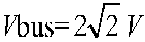
- It can be seen that, the pre-charge voltage of Cbus may reach two times of the voltage amplitude of the alternating current power source of the pre-charge circuit. In a case that the alternating current power source S is a phase voltage having an effective value denoted as V and an amplitude value denoted as


- A pre-charge function may be achieved by applying the circuit shown in
Figure 2a in a three-phase two-level photovoltaic inverter shown inFigure 3a , in which the auxiliary charging capacitor Caux and the switch current limiting device Z1 are connected in series between a neutral point N and a direct current side PV+ (or PV-) of an electrical grid, the alternating current power source is embodied directly as all or some of existing three phase voltages R, S and T, and the half-bridge rectifier is embodied directly as all or some of existing diodes D1 to D6 of an inverting circuit. Specifically, a complete pre-charge circuit may be formed by the phase voltage R, the diodes D1 and D2, a grid-connected switch S1, the auxiliary charging capacitor Caux and the switch current limiting device Z1. Another complete pre-charge circuit may be formed by the phase voltage S, the diodes D3 and D4, a grid-connected switch S2, Caux and Z1. Another complete pre-charge circuit may be formed by the phase voltage T, the diodes D5 and D6, the grid-connected switch S3, Caux and Z1. In addition, Z1 may be omitted since its function may be achieved by an alternating current reactor and the grid-connected switch of the photovoltaic inverter. - Further, the pre-charge function may be achieved by applying the circuit shown in
Figure 2a in a three-phase two level photovoltaic inverter shown inFigure 3b , in which the alternating current power source is embodied directly as an existing R-S line voltage or an existing R-T line voltage, the half-bridge rectifier is embodied directly as all or some of existing diodes D1 to D6 of an inverting circuit, and the auxiliary charging capacitor Caux and the switch current limiting device Z1 are connected in series between the R-S line voltage or R-T line voltage and a direct current side PV+ (or PV-). Specifically, a complete pre-charge circuit may be formed by the R-S line voltage, a grid-connected switch S2, the diodes D3 and D4, Caux and Z1. Another complete pre-charge circuit may be formed by the R-T line voltage, the grid-connected switch S3, the diodes D5 and D6, Caux and Z1. In addition, Z1 may be omitted, since its function may be achieved by an alternating current reactor and a grid-connected switch of the photovoltaic inverter. - Referring to
Figure 4a , a pre-charge circuit including one alternating current power source S, one half-bridge rectifier formed by diodes D1 and D2 connected in series and two auxiliary charging capacitors Caux1 and Caux2 is taken as an example. A switch current limiting device Z1 is connected in series on a charging path whereCaux 1 is located. A switch current limiting device Z3 is connected in series on a charging path where Caux2 is located. A switch current limiting device Z2 is connected in series on a charging path shared by Caux1 and Caux2. - In a case that the alternating current power source S supplies a forward voltage, two charging paths exist, as shown in
Figure 4b . In one of the charging paths, a current flows through Z2, D1, Cbus, Caux2 and Z3, thereby forming a charging loop to charge Cbus and Caux2. In the other charging path, a current flows through Z2, D1, Caux1 Z1, thereby forming a charging loop to charge Caux1 backwardly. In a case that the alternating current power source S supplies a backward voltage, two charging paths exist, as shown inFigure 4c . In one of the charging paths, a current flows through Z1, Caux1, Cbus, D2 and Z2, thereby forming a charging loop to charge Cbus and Caux1. In the other charging path, a current flows through Z3, Caux2, D2 and Z2, thereby forming a charging loop to charge Caux2 backwardly. - It is assumed that a voltage amplitude of the alternating current power source S is denoted as Vs, a steady-state voltage of Cbus is denoted as Vbus, a steady-state voltage of Caux1 is denoted as Vaux1 and a steady-state voltage of Caux2 is denoted as Vaux2. After the charging enters in a steady state, currents flowing through the two charging path in
Figure 4b and currents flowing through the two charging paths inFigure 4c each approach zero, that is, voltage drops of the switching current limiting devices Z1, Z2 and Z3 approach zero. If voltage drops of the diodes D1 and D2 in the loops are omitted, relations of voltages in the two charging loops inFigure 4b are respectively expressed as

Figure 4c are respectively expressed as


- As shown in
Figure 5a , a pre-charge circuit may include one alternating current power source S, one half-bridge rectifier formed by diodes D1 and D2 connected in series, two auxiliary charging capacitors Caux1 and Caux2 and several current limiting devices and controllable switches, in which the equation Vbus=2Vs is also satisfied and is not derived herein. A pre-charge function may be achieved by applying the circuit shown inFigure 5a in a three-phase three-level photovoltaic inverter shown inFigure 5b , in which the auxiliary charging capacitor Caux may be embodied directly as an existing positive bus capacitor C1 and an existing negative bus capacitor C2 in the inverter, a switching current limiting device Z1 is connected in series between a neutral point N and a direct current side PV+ (or PV-) of an electrical grid, the alternating current power source is embodied directly as all or some of existing three phase voltages R, S and T, and the half-bridge rectifier is embodied directly as all or some of existing diodes D1 to D6 of an inverting circuit. In addition, Z1 may be omitted, since its function may be achieved by an alternating current reactor and a grid-connected switch of the photovoltaic inverter. - A three-phase power source may be fully used for rectification to accelerate charging and improve a load capability of a direct current side of the inverter. As shown in
Figure 6 , a pre-charge circuit includes three alternating current power sources, three half-bridge rectifiers, one auxiliary charging capacitor Caux and four switching current limiting devices.Figure 6 differs fromFigure 2a only in the increased numbers of alternating current power sources and half-bridge rectifiers without changing the charging principle, which therefore can be understood by referring to descriptions related toFigures 2b and2c . - A pre-charge function may be achieved by applying the circuit shown in
Figure 6 in a three-phase two-level photovoltaic inverter shown inFigure 7 , in which an auxiliarycharging capacitor Caux 1, three half-bridge rectifiers and three switching current limiting devices Z1 to Z3 are added additionally. It can be seen by comparing withFigure 1 that, the circuit shown inFigure 7 is formed by adding Caux1 and Z3 to the circuit shown inFigure 1 (C1 is a normal capacitor for filtering and can be omitted). Certainly, a portion of components in the pre-charge circuit may be replaced with existing hardware of the photovoltaic inverter, to save a hardware cost. - In addition, it is further provided a photovoltaic inverter including any one of the above pre-charge circuits according to an embodiment of the present disclosure. In a case that the photovoltaic inverter meets a pre-charge condition (for example, when it is determined that the photovoltaic inverter operates in a static var generator mode, or when it is determined that the photovoltaic inverter is to be turned on under a high voltage of a photovoltaic battery or when a pre-charge instruction is received), a respective controllable switch is switched on to pre-charge a target charging capacitor. After the pre-charge of the target charging capacitor is finished, the controllable switch is switched off to end the pre-charge. Therefore, the issue of the low pre-charge voltage of the direct current bus is addressed, thereby avoiding a current impact generated when the photovoltaic inverter is electrically connected to a photovoltaic battery or when a grid-connection is performed.
- In summary, according to the present disclosure, with the voltage doubling rectifier circuit including the alternating current power source, the half-bridge rectifier, the auxiliary charging capacitor, the current limiting device, the controllable switch and the target charging capacitor, the target charging capacitor is pre-charged to raise a voltage across the target charging capacitor (i.e. a pre-charge voltage of a direct current bus) maximally to two times of a peak voltage of the alternating current power source. Therefore, the issue of the low pre-charge voltage of the direct current bus is addressed, thereby avoiding the current impact generated when the photovoltaic inverter is electrically connected to the photovoltaic battery or when a grid-connection is performed.
- In the present specification, the embodiments are described in a progressive manner. Each embodiment focuses on an aspect differences from other embodiments, and reference can be made to these similar parts among the embodiments.
- The above illustration of the disclosed embodiments enables those skilled in the art to implement or practice the present disclosure. Many changes to these embodiments are apparent for those skilled in the art, and general principles defined herein can be implemented in other embodiments without departing the spirit or scope of the present disclosure. Hence, the present disclosure is not limited to the embodiments disclosed herein, but is to conform to the widest scope consistent with principles and novel features disclosed herein.
Claims (10)
- A pre-charge circuit, comprising an alternating current power source, a half-bridge rectifier, an auxiliary charging capacitor, a current limiting device and a controllable switch, and the pre-charge circuit being connected to a target charging capacitor to form a voltage doubling rectifier circuit; wherein
a direct current side of the half-bridge rectifier is connected in parallel to the target charging capacitor, and an alternating current side of the half-bridge rectifier is connected to one end of the alternating current power source;
one end of the auxiliary charging capacitor is connected to any one end of the target charging capacitor, and the other end of the auxiliary charging capacitor is connected to the other end of the alternating current power source;
the current limiting device is connected in series on each charging path of the pre-charge circuit; and
the controllable switch is connected in series on each charging path of the pre-charge circuit. - The pre-charge circuit according to claim 1, wherein the alternating current power source is a phase voltage of an electrical grid or a line voltage of an electrical grid.
- The pre-charge circuit according to claim 1, wherein a semiconductor device in the half-bridge rectifier is a diode, a thyristor, a Metallic Oxide Semiconductor Field Effect Transistor (MOSFET) or an Insulated Gate Bipolar Transistor (IGBT) with anti-parallel diode.
- The pre-charge circuit according to claim 1, wherein the current limiting device is a resistor, an electrical-inductor, a choke coil, or any combination thereof.
- The pre-charge circuit according to claim 1, wherein the controllable switch is a relay, a Metallic Oxide Semiconductor Field Effect Transistor (MOSFET) or an Insulated Gate Bipolar Transistor (IGBT).
- The pre-charge circuit according to claim 1, wherein a semiconductor device in the half-bridge rectifier is an anti-parallel diode in an inverting circuit of a photovoltaic inverter.
- The pre-charge circuit according to claim 1, wherein the auxiliary charging capacitor is a positive bus capacitor and/or a negative bus capacitor on a direct current side of a photovoltaic inverter.
- The pre-charge circuit according to claim 1, wherein the current limiting device is an alternating current reactor of a photovoltaic inverter.
- The pre-charge circuit according to claim 1, wherein the controllable switch is a grid-connected switch of a photovoltaic inverter.
- A photovoltaic inverter, comprising the pre-charge circuit according to any one of claims 1 to 9.
Applications Claiming Priority (1)
| Application Number | Priority Date | Filing Date | Title |
|---|---|---|---|
| CN201510280409.8A CN104967300B (en) | 2015-05-27 | 2015-05-27 | A kind of pre-charge circuit and photovoltaic DC-to-AC converter |
Publications (2)
| Publication Number | Publication Date |
|---|---|
| EP3098953A2 true EP3098953A2 (en) | 2016-11-30 |
| EP3098953A3 EP3098953A3 (en) | 2016-12-14 |
Family
ID=54221287
Family Applications (1)
| Application Number | Title | Priority Date | Filing Date |
|---|---|---|---|
| EP16171181.7A Pending EP3098953A3 (en) | 2015-05-27 | 2016-05-24 | Pre-charge circuit and photovoltaic inverter |
Country Status (4)
| Country | Link |
|---|---|
| US (1) | US9912252B2 (en) |
| EP (1) | EP3098953A3 (en) |
| JP (1) | JP6295485B2 (en) |
| CN (1) | CN104967300B (en) |
Cited By (4)
| Publication number | Priority date | Publication date | Assignee | Title |
|---|---|---|---|---|
| CN110021955A (en) * | 2018-01-08 | 2019-07-16 | 丰郅(上海)新能源科技有限公司 | The method of the photovoltaic generating system and dynamic equilibrium electric energy of integrated energy storage function |
| EP3562016A1 (en) * | 2018-04-23 | 2019-10-30 | FRONIUS INTERNATIONAL GmbH | Precharging of an intermediate circuit |
| WO2022101425A1 (en) * | 2020-11-12 | 2022-05-19 | Sma Solar Technology Ag | Ac/dc converter for coupling a grounded ac supply system to an ungrounded dc supply system, precharging device, and insulation monitoring |
| EP3893388B1 (en) * | 2019-01-28 | 2023-11-22 | Huawei Digital Power Technologies Co., Ltd. | Device, method and system for solving common mode voltage interference |
Families Citing this family (15)
| Publication number | Priority date | Publication date | Assignee | Title |
|---|---|---|---|---|
| US9455645B1 (en) * | 2013-03-13 | 2016-09-27 | The Florida State University Research Foundation, Inc. | System and method for leakage current suppression in a photovoltaic cascaded multilevel inverter |
| FR3031849B1 (en) * | 2015-01-16 | 2017-02-17 | Alstom Transp Tech | POWER SUPPLY CONVERTER AND / OR SUBSTATION FOR RECOVERING BRAKING ENERGY |
| TWI542114B (en) * | 2015-06-17 | 2016-07-11 | 台達電子工業股份有限公司 | Photovoltaic inverter grid-connected system and method for implementing three-phase ac grid-connected transition |
| EP3157022A1 (en) * | 2015-10-16 | 2017-04-19 | SMA Solar Technology AG | Inductor assembly and power suppy system using the same |
| US10300791B2 (en) * | 2015-12-18 | 2019-05-28 | Ge Global Sourcing Llc | Trolley interfacing device having a pre-charging unit |
| CN105871205A (en) * | 2016-05-06 | 2016-08-17 | 华南理工大学 | Integrated multifunctional power source switching system |
| CN108063547B (en) * | 2016-11-08 | 2019-09-20 | 台达电子工业股份有限公司 | Pre-charging device and frequency converter |
| CN107612370A (en) * | 2017-09-19 | 2018-01-19 | 珠海格力电器股份有限公司 | Multichannel rectification circuit and Switching Power Supply altogether |
| CN108054998A (en) * | 2017-12-26 | 2018-05-18 | 深圳古瑞瓦特新能源股份有限公司 | A kind of optimizer, photovoltaic generating system and photovoltaic generation control method |
| CN108258669B (en) * | 2018-02-05 | 2022-11-25 | 全球能源互联网研究院有限公司 | Secondary phase-commutation type direct current limiter and control method thereof |
| US10855169B1 (en) * | 2019-09-10 | 2020-12-01 | Lear Corporation | Configurable multi-phase charger |
| JP7213166B2 (en) * | 2019-11-06 | 2023-01-26 | 株式会社日立産機システム | Power conversion device and press device |
| CN110994968B (en) * | 2019-11-22 | 2021-06-01 | 华为技术有限公司 | Pre-charging circuit, inverter and power generation system |
| US20210359621A1 (en) * | 2020-05-14 | 2021-11-18 | Eaton Intelligent Power Limited | Drive system with common dc bus |
| CN113489298A (en) * | 2021-08-20 | 2021-10-08 | 青岛鼎信通讯股份有限公司 | Pre-charging circuit applied to alternating current-direct current bidirectional inverter power supply module |
Family Cites Families (18)
| Publication number | Priority date | Publication date | Assignee | Title |
|---|---|---|---|---|
| JP3509531B2 (en) * | 1998-03-02 | 2004-03-22 | 三菱電機株式会社 | Switching converter |
| JP2004208408A (en) | 2002-12-25 | 2004-07-22 | Fuji Electric Holdings Co Ltd | Initial charging method of grid connected inverter |
| JP2005057949A (en) | 2003-08-07 | 2005-03-03 | Hitachi Industrial Equipment Systems Co Ltd | Power supply unit, semiconductor manufacturing apparatus and machine tool |
| WO2005048659A2 (en) * | 2003-11-06 | 2005-05-26 | Ceyx Technologies, Inc. | Method and apparatus for optimizing power efficiency in light emitting device arrays |
| JP2008136316A (en) | 2006-11-29 | 2008-06-12 | Daikin Ind Ltd | Charging device and method for power supply unit |
| US8482947B2 (en) * | 2009-07-31 | 2013-07-09 | Solarbridge Technologies, Inc. | Apparatus and method for controlling DC-AC power conversion |
| EP2564502A4 (en) * | 2010-04-26 | 2018-01-24 | Queen's University At Kingston | Power converter for a power generator |
| JP2012222854A (en) | 2011-04-04 | 2012-11-12 | Mitsubishi Electric Corp | Power conversion system |
| US8619396B2 (en) * | 2011-06-24 | 2013-12-31 | Renewable Power Conversion, Inc. | Renewable one-time load break contactor |
| JP2013031309A (en) | 2011-07-29 | 2013-02-07 | Noritz Corp | Power conditioner |
| CN102916437B (en) * | 2011-12-24 | 2015-08-26 | 许继电气股份有限公司 | The soft combination method of a kind of grid-connected converter |
| JP2013162591A (en) | 2012-02-03 | 2013-08-19 | Sekisui Chem Co Ltd | Power supply circuit and electronic device |
| JP2014107931A (en) | 2012-11-27 | 2014-06-09 | Fuji Electric Co Ltd | Method for operating inverter device, and inverter device |
| IN2013MU01204A (en) * | 2013-03-28 | 2015-04-10 | Control Tech Ltd | |
| GB2521683B (en) * | 2013-12-19 | 2016-04-20 | Control Tech Ltd | Capacitor failure |
| US9490704B2 (en) * | 2014-02-12 | 2016-11-08 | Delta Electronics, Inc. | System and methods for controlling secondary side switches in resonant power converters |
| FI10496U1 (en) * | 2014-02-20 | 2014-05-22 | Abb Oy | Capacitor Charger |
| CN104300777B (en) * | 2014-11-07 | 2017-06-23 | 深圳市永联科技股份有限公司 | A kind of inverter synchronization combination method |
-
2015
- 2015-05-27 CN CN201510280409.8A patent/CN104967300B/en active Active
-
2016
- 2016-05-24 EP EP16171181.7A patent/EP3098953A3/en active Pending
- 2016-05-25 JP JP2016103805A patent/JP6295485B2/en active Active
- 2016-05-25 US US15/164,069 patent/US9912252B2/en active Active
Non-Patent Citations (1)
| Title |
|---|
| None |
Cited By (6)
| Publication number | Priority date | Publication date | Assignee | Title |
|---|---|---|---|---|
| CN110021955A (en) * | 2018-01-08 | 2019-07-16 | 丰郅(上海)新能源科技有限公司 | The method of the photovoltaic generating system and dynamic equilibrium electric energy of integrated energy storage function |
| EP3562016A1 (en) * | 2018-04-23 | 2019-10-30 | FRONIUS INTERNATIONAL GmbH | Precharging of an intermediate circuit |
| WO2019206910A1 (en) * | 2018-04-23 | 2019-10-31 | Fronius International Gmbh | Precharging of an intermediate circuit |
| AU2019258117B2 (en) * | 2018-04-23 | 2021-08-19 | Fronius International Gmbh | Precharging of an intermediate circuit |
| EP3893388B1 (en) * | 2019-01-28 | 2023-11-22 | Huawei Digital Power Technologies Co., Ltd. | Device, method and system for solving common mode voltage interference |
| WO2022101425A1 (en) * | 2020-11-12 | 2022-05-19 | Sma Solar Technology Ag | Ac/dc converter for coupling a grounded ac supply system to an ungrounded dc supply system, precharging device, and insulation monitoring |
Also Published As
| Publication number | Publication date |
|---|---|
| CN104967300B (en) | 2018-04-10 |
| CN104967300A (en) | 2015-10-07 |
| JP2016226272A (en) | 2016-12-28 |
| US20160352252A1 (en) | 2016-12-01 |
| JP6295485B2 (en) | 2018-03-20 |
| EP3098953A3 (en) | 2016-12-14 |
| US9912252B2 (en) | 2018-03-06 |
Similar Documents
| Publication | Publication Date | Title |
|---|---|---|
| EP3098953A2 (en) | Pre-charge circuit and photovoltaic inverter | |
| CN109391166B (en) | Conversion circuit, control method and power supply equipment | |
| US10263429B2 (en) | Bidirectional DC-DC converter, power conditioner, and distributed power system | |
| US9041251B2 (en) | Boost converter with multiple inputs and inverter circuit | |
| US20140334199A1 (en) | Five-Level Power Converter, and Control Method and Control Apparatus for the Same | |
| JP5254357B2 (en) | Power converter | |
| EP2933909B1 (en) | Converter and voltage clamp circuit therein | |
| US20220085756A1 (en) | Inverter circuit, inverter, and photovoltaic power system | |
| US20140153287A1 (en) | System and method for improving power conversion efficiency | |
| US20160308458A1 (en) | Power conversion device | |
| US20120025609A1 (en) | Very high efficiency uninterruptible power supply | |
| US10666143B2 (en) | Control device for direct power converter | |
| US20170005590A1 (en) | Power converter | |
| EP3273588B1 (en) | Inverter circuit and power conversion device | |
| US9337748B2 (en) | System and method for a DC-to-DC power converter with inverter stage coupled to the DC input | |
| CN102379081A (en) | Power conversion apparatus | |
| US9431924B2 (en) | Power source inverter for use with a photovoltaic solar panel | |
| EP2993777B1 (en) | Multilevel converter | |
| US8779710B2 (en) | Inverter device | |
| US9571002B2 (en) | Voltage adjusting apparatus | |
| EP2893628B1 (en) | Interleaved 12-pulse rectifier | |
| US20220173652A1 (en) | Power conversion system and virtual dc voltage generator circuit | |
| CN107925361A (en) | Multi-electrical level inverter topological circuit | |
| US20220200480A1 (en) | Power conversion system, method for controlling the power conversion system, and program | |
| CN109449992A (en) | Converter side common mode voltage suppression device and method, converter and fan |
Legal Events
| Date | Code | Title | Description |
|---|---|---|---|
| PUAI | Public reference made under article 153(3) epc to a published international application that has entered the european phase |
Free format text: ORIGINAL CODE: 0009012 |
|
| PUAL | Search report despatched |
Free format text: ORIGINAL CODE: 0009013 |
|
| AK | Designated contracting states |
Kind code of ref document: A2 Designated state(s): AL AT BE BG CH CY CZ DE DK EE ES FI FR GB GR HR HU IE IS IT LI LT LU LV MC MK MT NL NO PL PT RO RS SE SI SK SM TR |
|
| AX | Request for extension of the european patent |
Extension state: BA ME |
|
| AK | Designated contracting states |
Kind code of ref document: A3 Designated state(s): AL AT BE BG CH CY CZ DE DK EE ES FI FR GB GR HR HU IE IS IT LI LT LU LV MC MK MT NL NO PL PT RO RS SE SI SK SM TR |
|
| AX | Request for extension of the european patent |
Extension state: BA ME |
|
| RIC1 | Information provided on ipc code assigned before grant |
Ipc: H02M 1/36 20070101AFI20161110BHEP Ipc: H02M 7/5387 20070101ALN20161110BHEP Ipc: H02M 7/797 20060101ALN20161110BHEP Ipc: H02M 7/12 20060101ALI20161110BHEP Ipc: H02M 7/219 20060101ALN20161110BHEP Ipc: H02J 3/38 20060101ALN20161110BHEP |
|
| STAA | Information on the status of an ep patent application or granted ep patent |
Free format text: STATUS: REQUEST FOR EXAMINATION WAS MADE |
|
| 17P | Request for examination filed |
Effective date: 20170614 |
|
| RBV | Designated contracting states (corrected) |
Designated state(s): AL AT BE BG CH CY CZ DE DK EE ES FI FR GB GR HR HU IE IS IT LI LT LU LV MC MK MT NL NO PL PT RO RS SE SI SK SM TR |
|
| STAA | Information on the status of an ep patent application or granted ep patent |
Free format text: STATUS: EXAMINATION IS IN PROGRESS |
|
| 17Q | First examination report despatched |
Effective date: 20180208 |
|
| STAA | Information on the status of an ep patent application or granted ep patent |
Free format text: STATUS: EXAMINATION IS IN PROGRESS |
|
| STAA | Information on the status of an ep patent application or granted ep patent |
Free format text: STATUS: EXAMINATION IS IN PROGRESS |