JP5254357B2 - Power converter - Google Patents
Power converter Download PDFInfo
- Publication number
- JP5254357B2 JP5254357B2 JP2010541952A JP2010541952A JP5254357B2 JP 5254357 B2 JP5254357 B2 JP 5254357B2 JP 2010541952 A JP2010541952 A JP 2010541952A JP 2010541952 A JP2010541952 A JP 2010541952A JP 5254357 B2 JP5254357 B2 JP 5254357B2
- Authority
- JP
- Japan
- Prior art keywords
- voltage
- switch
- inverter circuit
- circuit
- input
- Prior art date
- Legal status (The legal status is an assumption and is not a legal conclusion. Google has not performed a legal analysis and makes no representation as to the accuracy of the status listed.)
- Active
Links
- 239000003990 capacitor Substances 0.000 claims description 41
- 238000009499 grossing Methods 0.000 claims description 40
- 239000004065 semiconductor Substances 0.000 claims description 29
- 238000006243 chemical reaction Methods 0.000 claims description 14
- 238000007599 discharging Methods 0.000 claims description 7
- 230000001360 synchronised effect Effects 0.000 claims description 6
- 238000010586 diagram Methods 0.000 description 16
- 238000013459 approach Methods 0.000 description 5
- 230000000694 effects Effects 0.000 description 4
- 230000002441 reversible effect Effects 0.000 description 4
- 230000001052 transient effect Effects 0.000 description 3
- 230000003111 delayed effect Effects 0.000 description 2
- 230000003247 decreasing effect Effects 0.000 description 1
- 230000005669 field effect Effects 0.000 description 1
- 229910044991 metal oxide Inorganic materials 0.000 description 1
- 150000004706 metal oxides Chemical class 0.000 description 1
- 238000012544 monitoring process Methods 0.000 description 1
Images


Classifications
-
- H—ELECTRICITY
- H02—GENERATION; CONVERSION OR DISTRIBUTION OF ELECTRIC POWER
- H02M—APPARATUS FOR CONVERSION BETWEEN AC AND AC, BETWEEN AC AND DC, OR BETWEEN DC AND DC, AND FOR USE WITH MAINS OR SIMILAR POWER SUPPLY SYSTEMS; CONVERSION OF DC OR AC INPUT POWER INTO SURGE OUTPUT POWER; CONTROL OR REGULATION THEREOF
- H02M1/00—Details of apparatus for conversion
- H02M1/42—Circuits or arrangements for compensating for or adjusting power factor in converters or inverters
- H02M1/4208—Arrangements for improving power factor of AC input
- H02M1/4225—Arrangements for improving power factor of AC input using a non-isolated boost converter
-
- H—ELECTRICITY
- H02—GENERATION; CONVERSION OR DISTRIBUTION OF ELECTRIC POWER
- H02M—APPARATUS FOR CONVERSION BETWEEN AC AND AC, BETWEEN AC AND DC, OR BETWEEN DC AND DC, AND FOR USE WITH MAINS OR SIMILAR POWER SUPPLY SYSTEMS; CONVERSION OF DC OR AC INPUT POWER INTO SURGE OUTPUT POWER; CONTROL OR REGULATION THEREOF
- H02M1/00—Details of apparatus for conversion
- H02M1/12—Arrangements for reducing harmonics from ac input or output
-
- H—ELECTRICITY
- H02—GENERATION; CONVERSION OR DISTRIBUTION OF ELECTRIC POWER
- H02M—APPARATUS FOR CONVERSION BETWEEN AC AND AC, BETWEEN AC AND DC, OR BETWEEN DC AND DC, AND FOR USE WITH MAINS OR SIMILAR POWER SUPPLY SYSTEMS; CONVERSION OF DC OR AC INPUT POWER INTO SURGE OUTPUT POWER; CONTROL OR REGULATION THEREOF
- H02M1/00—Details of apparatus for conversion
- H02M1/0083—Converters characterised by their input or output configuration
- H02M1/0085—Partially controlled bridges
-
- H—ELECTRICITY
- H02—GENERATION; CONVERSION OR DISTRIBUTION OF ELECTRIC POWER
- H02M—APPARATUS FOR CONVERSION BETWEEN AC AND AC, BETWEEN AC AND DC, OR BETWEEN DC AND DC, AND FOR USE WITH MAINS OR SIMILAR POWER SUPPLY SYSTEMS; CONVERSION OF DC OR AC INPUT POWER INTO SURGE OUTPUT POWER; CONTROL OR REGULATION THEREOF
- H02M7/00—Conversion of ac power input into dc power output; Conversion of dc power input into ac power output
- H02M7/02—Conversion of ac power input into dc power output without possibility of reversal
- H02M7/04—Conversion of ac power input into dc power output without possibility of reversal by static converters
- H02M7/12—Conversion of ac power input into dc power output without possibility of reversal by static converters using discharge tubes with control electrode or semiconductor devices with control electrode
- H02M7/21—Conversion of ac power input into dc power output without possibility of reversal by static converters using discharge tubes with control electrode or semiconductor devices with control electrode using devices of a triode or transistor type requiring continuous application of a control signal
- H02M7/217—Conversion of ac power input into dc power output without possibility of reversal by static converters using discharge tubes with control electrode or semiconductor devices with control electrode using devices of a triode or transistor type requiring continuous application of a control signal using semiconductor devices only
-
- Y—GENERAL TAGGING OF NEW TECHNOLOGICAL DEVELOPMENTS; GENERAL TAGGING OF CROSS-SECTIONAL TECHNOLOGIES SPANNING OVER SEVERAL SECTIONS OF THE IPC; TECHNICAL SUBJECTS COVERED BY FORMER USPC CROSS-REFERENCE ART COLLECTIONS [XRACs] AND DIGESTS
- Y02—TECHNOLOGIES OR APPLICATIONS FOR MITIGATION OR ADAPTATION AGAINST CLIMATE CHANGE
- Y02B—CLIMATE CHANGE MITIGATION TECHNOLOGIES RELATED TO BUILDINGS, e.g. HOUSING, HOUSE APPLIANCES OR RELATED END-USER APPLICATIONS
- Y02B70/00—Technologies for an efficient end-user side electric power management and consumption
- Y02B70/10—Technologies improving the efficiency by using switched-mode power supplies [SMPS], i.e. efficient power electronics conversion e.g. power factor correction or reduction of losses in power supplies or efficient standby modes
Landscapes
- Engineering & Computer Science (AREA)
- Power Engineering (AREA)
- Inverter Devices (AREA)
- Rectifiers (AREA)
Description
この発明は、入力力率を改善する回路を備えて交流電力を直流電力に変換する電力変換装置に関するものである。 The present invention relates to a power conversion device that includes a circuit that improves an input power factor and converts AC power into DC power.
従来の電力変換装置には、以下に示す昇圧形交直変換回路がある。交流電源とダイオード整流回路との接続点にリアクトルを挿入し、ダイオード整流回路の出力端子間に主スイッチング素子を接続し、この主スイッチング素子と並列にコンデンサとダイオードの直列回路を接続し、コンデンサの両端間を直流出力とする。そして、ダイオード整流回路と主スイッチング素子との間に、それぞれダイオードとスイッチング素子とを直列接続した2つの直列回路とコンデンサとを互いに並列接続したブリッジ回路を挿入することにより、昇圧形交直変換回路における入力電流の高調波を低減させる(例えば、特許文献1参照)。 A conventional power converter includes a step-up AC / DC converter circuit shown below. A reactor is inserted at the connection point between the AC power supply and the diode rectifier circuit, a main switching element is connected between the output terminals of the diode rectifier circuit, and a series circuit of a capacitor and a diode is connected in parallel with the main switching element. DC output between both ends. In the step-up AC / DC converter circuit, a bridge circuit in which two series circuits each having a diode and a switching element connected in series and a capacitor are connected in parallel is inserted between the diode rectifier circuit and the main switching element. The harmonics of the input current are reduced (see, for example, Patent Document 1).
このような電力変換装置では、インバータ(ブリッジ回路)のコンデンサの充放電を制御して入力電流の高調波を低減しているため、インバータ直流母線電圧を安定化するためには、外部に直流電圧源を接続する必要がある。また、交流入力電源および負荷の過渡的な変化に対して、外部に接続した直流電圧源の供給能力が十分大きく無ければ、インバータの直流母線電圧が変動するため、装置の安定動作が困難となる。 In such a power converter, since the harmonics of the input current are reduced by controlling the charging / discharging of the capacitor of the inverter (bridge circuit), in order to stabilize the inverter DC bus voltage, an external DC voltage is required. You need to connect the source. Moreover, if the supply capacity of the DC voltage source connected to the outside is not sufficiently large with respect to the transient change of the AC input power supply and the load, the DC bus voltage of the inverter fluctuates, which makes it difficult to stably operate the device. .
この発明は、上記のような問題点を解消するために成されたものであって、単相インバータを備えて入力力率を改善する入力電流制御と出力段の電圧制御とを行い、交流電力を直流電力に変換する電力変換装置において、単相インバータの直流母線電圧を、外部に電圧源を要することなく安定化させ、電力変換装置を安定して動作させることを目的とする。 The present invention has been made to solve the above problems, and includes an input current control for improving an input power factor provided with a single-phase inverter and an output stage voltage control, and an AC power. An object of the present invention is to stabilize the DC bus voltage of a single-phase inverter without requiring an external voltage source and to stably operate the power converter.
この発明に係る電力変換装置は、交流入力電源からの入力を整流する整流回路と、それぞれ複数の半導体スイッチ素子と直流電圧源とを有する1以上の単相インバータの交流側を直列接続して構成され、該交流側を上記整流回路の出力に直列接続して上記各単相インバータの出力の総和を上記整流回路の出力に重畳するインバータ回路と、該インバータ回路の後段に整流ダイオードを介して接続され該出力を平滑する平滑コンデンサと、上記インバータ回路に一端が接続され、他端が上記平滑コンデンサの一端に接続されて、上記平滑コンデンサをバイパスさせる短絡用スイッチとを備える。そして、上記インバータ回路は、上記平滑コンデンサの電圧を第1の目標電圧に追従させると共に上記交流入力電源からの入力力率を改善するように、電流指令を用いて出力制御され、上記短絡用スイッチは、上記インバータ回路内の上記直流電圧源の電圧を第2の目標電圧に追従させるように、オン/オフ制御されるものである。 A power conversion device according to the present invention is configured by connecting in series an AC side of one or more single-phase inverters each having a rectifier circuit that rectifies an input from an AC input power source, and a plurality of semiconductor switch elements and a DC voltage source. An inverter circuit in which the AC side is connected in series to the output of the rectifier circuit and the sum of the outputs of the single-phase inverters is superimposed on the output of the rectifier circuit, and connected to the subsequent stage of the inverter circuit via a rectifier diode And a smoothing capacitor for smoothing the output, and a short-circuit switch having one end connected to the inverter circuit and the other end connected to one end of the smoothing capacitor to bypass the smoothing capacitor. The inverter circuit is output-controlled using a current command so as to cause the voltage of the smoothing capacitor to follow the first target voltage and to improve the input power factor from the AC input power supply, and the short-circuit switch Is controlled on / off so that the voltage of the DC voltage source in the inverter circuit follows the second target voltage.
この発明によると、短絡用スイッチの制御により、インバータ回路内の直流電圧源の電圧が第2の目標電圧に制御されるため、単相インバータの直流母線電圧を、外部に電圧源を要することなく安定化でき、電力変換装置を安定して動作させることができる。 According to the present invention, since the voltage of the DC voltage source in the inverter circuit is controlled to the second target voltage by the control of the short-circuit switch, the DC bus voltage of the single-phase inverter can be reduced without requiring an external voltage source. The power converter can be operated stably.
実施の形態1.
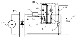
以下、この発明の実施の形態1による電力変換装置について説明する。図1はこの発明の実施の形態1による電力変換装置の概略構成図である。
図1に示すように、交流入力電源としての交流電圧電源1(以下、単に交流電源1と称す)は整流回路としてのダイオードブリッジ2に接続される。ダイオードブリッジ2の出力は限流成分としてのリアクトル3に接続され、その後段に単相インバータにて構成されたインバータ回路100の交流側が直列接続される。インバータ回路100を構成する単相インバータは半導体スイッチ素子4、5、ダイオード6、7および直流電圧源8から構成される。ここで、半導体スイッチ素子4、5は、ダイオードが逆並列に接続されたIGBT(Insulated Gate Bipolar Transistor)やソース・ドレイン間にダイオードが内蔵されたMOSFET(Metal Oxide Semiconductor Field Effect Transistor)などを用い、またダイオード6、7の代わりに、半導体スイッチ素子4、5と同様に半導体スイッチ素子を配置してもよい。また、リアクトル3はインバータ回路100の後段に直列接続しても良い。
Hereinafter, a power converter according to
As shown in FIG. 1, an AC voltage power source 1 (hereinafter simply referred to as AC power source 1) as an AC input power source is connected to a
またインバータ回路100の後段には短絡用スイッチ9と整流ダイオード10とが接続され、整流ダイオード10のカソード側が出力段の平滑コンデンサ11の正極に接続される。ここでは、短絡用スイッチ9と整流ダイオード10のアノードとの接続点がインバータ回路100の後段の交流出力線に接続され、短絡用スイッチ9の他端は平滑コンデンサ11の負極に接続される。
また、平滑コンデンサ11およびインバータ回路100の直流電圧源8には、それぞれ電圧を監視する手段となる電圧検出器12、13を設け、検出された各電圧は駆動制御部15に入力され、駆動制御部15からの駆動信号16、17によりインバータ回路100内の半導体スイッチ素子4、5および短絡用スイッチ9はオン/オフ制御される。Further, a
Further, the
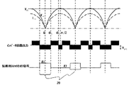
このように構成される電力変換装置の動作について、図2に示す各部の波形に基づいて説明する。
交流電源1からの入力はダイオードブリッジ2にて全波整流され、ダイオードブリッジ2の後段の電圧Vin、電流Iinは、図2に示すような波形となる。Vdcは、第1の目標電圧としての一定の目標電圧Vdc*に制御される平滑コンデンサ11の直流電圧であり、この場合、電圧Vinのピーク電圧が平滑コンデンサ11の直流電圧Vdcより高いものとする。
インバータ回路100は、交流電源1からの入力力率が概1になるようにPWM制御により電流Iinを制御して出力し、交流側の発生電圧をダイオードブリッジ2後段の電圧Vinに重畳する。インバータ回路100内の電流は、図3〜図5に示すように、半導体スイッチ素子4、5がオフの時には、ダイオード6を通って直流電圧源8を充電し、ダイオード7を通って出力される。また、半導体スイッチ素子4のみをオンした時には、電流は半導体スイッチ素子4とダイオード7とを通って出力される。また同様に、半導体スイッチ素子5のみをオンした時には、電流はダイオード6と半導体スイッチ素子5を通って出力される。また、半導体スイッチ素子4、5を同時にオンした時には、半導体スイッチ素子4を通って直流電圧源8を放電し、半導体スイッチ素子5を通って出力される。このような4種の制御の組み合わせにて半導体スイッチ素子4、5を制御してインバータ回路100をPWM制御する。The operation of the power conversion device configured as described above will be described based on the waveforms of the respective units shown in FIG.
The input from the
The
交流電源1からの入力電圧位相をθとし、電圧Vinが平滑コンデンサ11の目標電圧Vdc*と等しくなる時の位相θ=θ2(0<θ2<π/2)とする。短絡用スイッチ9は、ゼロクロス位相である位相θ=nπ(nは整数)を含む期間:nπ−θ1<θ<nπ+θ1(0<θ1<θ2)(以下、オン期間20と称す)でのみオン状態となり、平滑コンデンサ11をバイパスさせる。なお、短絡用スイッチ9の制御の詳細は後述する。
The phase of the input voltage from the
位相θが0≦θ≦π/2である間の動作を以下に説明する。
まず、位相θが0≦θ≦θ1である時は、短絡用スイッチ9のオン期間20内であり、図3に示すように、交流電源1からの電流は、交流電源1→ダイオードブリッジ2→リアクトル3→インバータ回路100→短絡用スイッチ9→ダイオードブリッジ2→交流電源1の経路で流れる。短絡用スイッチ9はオン状態なので、整流ダイオード10および出力段の平滑コンデンサ11には電流が流れない。インバータ回路100は、PWM制御により、例えば、半導体スイッチ素子4、5がオフの場合と、半導体スイッチ素子4のみをオンの場合とを組み合わせて電圧Vinの逆極性にほぼ等しい電圧を発生させつつ、入力力率が概1になるように電流Iinを制御して出力し、この間、インバータ回路100の直流電圧源8にはエネルギが充電される。The operation while the phase θ is 0 ≦ θ ≦ π / 2 will be described below.
First, when the phase θ is 0 ≦ θ ≦ θ1, it is within the
次に、位相θ=θ1の時、短絡用スイッチ9がオフすると、図4に示すように、交流電源1からの電流は、交流電源1→ダイオードブリッジ2→リアクトル3→インバータ回路100→整流ダイオード10→平滑コンデンサ11→ダイオードブリッジ2→交流電源1の経路で流れる。
位相θが、θ1≦θ≦θ2である時、インバータ回路100はPWM制御により、例えば、半導体スイッチ素子4、5が同時にオンの場合と、半導体スイッチ素子4のみをオンの場合とを組み合わせて出力する。この時、平滑コンデンサ11の直流電圧Vdcが目標電圧Vdc*に維持できるように、Vdc*−Vinにほぼ等しい電圧を発生させつつ、入力力率が概1になるように電流Iinを制御して出力する。この間、インバータ回路100が発生する電圧極性と電流Iinの極性は等しくなるので、インバータ回路100の直流電圧源8は放電される。Next, when the short-
When the phase θ is θ1 ≦ θ ≦ θ2, the
次に、位相θ=θ2にて電圧Vinが平滑コンデンサ11の直流電圧Vdc*と等しくなると、短絡用スイッチ9はオフ状態を継続するが、インバータ回路100での動作が変わる。
即ち位相θが、θ2≦θ≦π/2である時、図5に示すように、交流電源1からの電流は、交流電源1→ダイオードブリッジ2→リアクトル3→インバータ回路100→整流ダイオード10→平滑コンデンサ11→ダイオードブリッジ2→交流電源1の経路で流れる。また、インバータ回路100はPWM制御により、例えば、半導体スイッチ素子4、5がオフの場合と、半導体スイッチ素子5のみをオンの場合とを組み合わせて出力する。この時、平滑コンデンサ11の目標電圧Vdc*≦電圧Vinであり、インバータ回路100は、平滑コンデンサ11の直流電圧Vdcが目標電圧Vdc*に維持できるように、Vin−Vdc*にほぼ等しい電圧をVinの極性に対して逆極性に発生させつつ、入力力率が概1になるように電流Iinを制御して出力する。この間、インバータ回路100が発生する電圧極性と電流Iinの極性は逆になるので、インバータ回路100の直流電圧源8は充電される。Next, when the voltage Vin becomes equal to the DC voltage Vdc * of the smoothing
That is, when the phase θ is θ2 ≦ θ ≦ π / 2, as shown in FIG. 5, the current from the
図に示すように、π/2≦θ≦πの位相期間では、上述した0≦θ≦π/2の位相期間と対称の動作をし、π≦θ≦2πの位相期間では、0≦θ≦πの位相期間と同様である。
上述したように、短絡用スイッチ9をオン状態として平滑コンデンサ11をバイパスさせるオン期間20は、交流電源1からの入力電圧の位相θのゼロクロス位相である位相θ=nπ(nは整数)を含む所定の期間のみである。このとき、インバータ回路100は、電圧Vinの逆極性にほぼ等しい電圧を発生させつつ、入力力率が概1になるように電流Iinを制御して出力し、直流電圧源8は充電される。そして、オン期間20以外の位相では、インバータ回路100は、平滑コンデンサ11の直流電圧Vdcを目標電圧Vdc*に維持し、また入力力率が概1になるように電流Iinを制御して出力する。このとき、電圧Vinが平滑コンデンサ11の目標電圧Vdc*以下の時、直流電圧源8は放電され、電圧Vinが目標電圧Vdc*以上の時は、直流電圧源8は充電される。As shown in the figure, the phase period of π / 2 ≦ θ ≦ π operates symmetrically with the phase period of 0 ≦ θ ≦ π / 2 described above, and 0 ≦ θ in the phase period of π ≦ θ ≦ 2π. It is the same as the phase period of ≦ π.
As described above, the
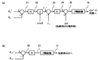
次に、駆動制御部15での制御の詳細を、図6に示すよう制御ブロックに基づいて以下に説明する。図6(a)は、インバータ回路100の制御を示す図であり、図6(b)は、短絡用スイッチ9の制御を示す図である。
図6(a)に示すようにインバータ回路100の制御では、電圧検出器12にて検出された平滑コンデンサ11の直流電圧Vdcと予め設定された平滑コンデンサの目標電圧Vdc*との差21を0に近づけるように、フィードバック制御(PI制御)して電流Iinの振幅目標値22を決定する。そして、この振幅目標値22に基づいて、電圧Vinに同期した正弦波の電流指令Iin*を生成する。Next, details of the control in the
As shown in FIG. 6A, in the control of the
次に、電流指令Iin*と検出された電流Iinとの差23を0に近づけるようにフィードバック制御(PI制御)して、インバータ回路100の発生電圧の目標値となる電圧指令24を出力する。この時、短絡用スイッチ9のオン/オフ切り替え時に同期したフィードフォワード補正電圧ΔVを加算して電圧指令24を補正する。
上述したように短絡用スイッチ9をオンからオフに切り替えるとインバータ回路100の直流電圧源8は充電から放電に切り替わり、短絡用スイッチ9がオフからオンに切り替わると直流電圧源8は放電から充電に切り替わる。このオン/オフ切り替え時にフィードフォワード制御を用いることで、フィードバック制御の応答時間分の制御遅れ、および限流用のリアクトル3の両端に発生する電圧をキャンセルすることができる。これにより、短絡用スイッチ9のオン/オフに起因する電流の急激な変化を緩和することができる。なお、フィードフォワード補正電圧ΔVは、短絡用スイッチ9をオンからオフにする際には正極性の電圧で、短絡用スイッチ9をオフからオンにする際には負極性の電圧である。Next, feedback control (PI control) is performed so that the
As described above, when the short-
そして、補正後の電圧指令25(短絡用スイッチ9のオン/オフ切り替え時以外は補正前電圧指令24)を用いて、PWM制御によりインバータ回路100の各半導体スイッチ素子4、5への各駆動信号16を生成し、インバータ回路100を動作させる。
Then, using the corrected voltage command 25 (
一方、図6(b)に示すように短絡用スイッチ9の制御では、電圧検出器13にて検出されたインバータ回路100の直流電圧源8の電圧Vsubを監視し、予め設定された第2の目標電圧としての直流電圧源8の目標電圧Vsub*との差26を0に近づけるように、フィードバック制御(PI制御)した出力27を用いて、PWM制御により短絡用スイッチ9への駆動信号17を生成し、短絡用スイッチ9がオン状態となる位相、即ちオン期間20を制御する。
なお、短絡用スイッチ9をPWM制御する際のキャリア波には、図7に示すように、ゼロ位相が交流電源1からの入力電圧のゼロクロス位相と同期し、入力電圧の半波毎に1つの三角波形を出力する三角波を用いる。これにより、オン期間20は、交流電源1からの入力電圧の位相θのゼロクロス位相を含む期間のみとなる。On the other hand, as shown in FIG. 6B, in the control of the short-
As shown in FIG. 7, the carrier wave when PWM controlling the short-
このような短絡用スイッチ9の制御では、直流電圧源8の電圧Vsubを目標電圧Vsub*から減算した電圧値が高いほど、短絡用スイッチ9のオン期間が長くなる。このため、過渡的な負荷変動や交流電源1の変動によって電圧Vsubが変動した場合でも、直流電圧源8を充電する時間を制御する事ができ、直流電圧源8の電圧Vsubを一定に制御する事が可能となる。従って、外部に別の直流電圧源を要することなく、交流電源1および負荷の過渡的な変化に対しても、インバータ回路100の直流電圧源8の電圧を安定化でき、インバータ回路100の直流母線電圧を一定に保つ事できるため、電力変換装置を安定して動作させることができる。
また、交流電源1からの入力電圧のゼロクロス位相の近傍が短絡用スイッチ9のオン期間20に含まれるため、電圧Vinが低い領域で平滑コンデンサ11へ出力する必要がなく、インバータ回路100の直流電圧を低く構成できる。In such control of the shorting
Further, since the vicinity of the zero-cross phase of the input voltage from the
また、この実施の形態では、電流指令Iin*を用いてインバータ回路100を制御することにより、平滑コンデンサ11の直流電圧Vdcを目標電圧Vdc*に追従させ、交流電源1からの入力力率を改善するように制御する。短絡用スイッチ9は高周波スイッチングが不要であり、入力力率を改善し出力段の直流電圧Vdcを制御するインバータ回路100は、スイッチングで扱う電圧を交流電源1のピーク電圧よりも大幅に低くできる。このため、大きなリアクトル3を要することなくスイッチング損失およびノイズを低減できる。また、短絡用スイッチ9がオン状態の時は、平滑コンデンサ11をバイパスしてインバータ回路100の直流電圧源8を充電できるため、インバータ回路100が高い電圧を発生させることなく電流0となるのが回避できると共に、充電されたエネルギを平滑コンデンサ11への放電に使える。このため、スイッチングで扱う電圧をさらに低減でき、高効率化、低ノイズ化がさらに促進できる。
In this embodiment, by controlling the
なお、上記実施の形態では、交流電源1からの入力電圧のゼロクロス位相がオン期間20(nπ−θ1<θ<nπ+θ1)の中央となるものを説明したが、オンに切り替わるタイミングとオフに切り替わるタイミングとの双方をそれぞれをPWM制御により検出してオン期間20を決定しても良い。
In the above-described embodiment, the case where the zero-cross phase of the input voltage from the
また、上記実施の形態1では、インバータ回路100は、1つの単相インバータで構成されたものを示したが、図8に示すように、複数個の単相インバータ100a、100bの交流側を直列接続してインバータ回路200を構成しても良く、上記実施の形態と同様の効果を奏する。
この場合、各単相インバータ100a、100bの出力の総和が、インバータ回路200の出力となり、駆動制御部15aでは、上記実施の形態と同様に、電流指令を用いて平滑コンデンサ11の直流電圧Vdcを目標電圧Vdc*に追従させ、交流電源1からの入力力率を改善するように、各単相インバータ100a、100b内の各半導体スイッチング素子4、5への各駆動信号16aを生成してインバータ回路200を制御する。そして、各単相インバータ100a、100bの各直流電圧源8の電圧を監視し、これらの電圧和を目標電圧に追従させるようにPWM制御により駆動信号17を生成して短絡用スイッチ9を制御する。In the first embodiment, the
In this case, the sum of the outputs of the single-
さらに、上記実施の形態1では短絡用スイッチ9の一端は、インバータ回路100の交流出力線に接続したが、図9に示すように、短絡用スイッチ9aの一端は、インバータ回路100を構成する直流電圧源8の負極側に接続しても良い。短絡用スイッチ9aの他端は、上記実施の形態1と同様に、平滑コンデンサ11の負極側、即ちダイオードブリッジ2の一端に接続される。
この場合、インバータ回路100および短絡用スイッチ9aの制御は、上記実施の形態1と同様であるが、短絡用スイッチ9aがオン状態であるオン期間20では、電流経路は図10に示すようになる。交流電源1からの電流は、交流電源1→ダイオードブリッジ2→リアクトル3→インバータ回路100の半導体スイッチ素子4→短絡用スイッチ9a→ダイオードブリッジ2→交流電源1の経路、または、交流電源1→ダイオードブリッジ2→リアクトル3→インバータ回路100のダイオード6→直流電圧源8→短絡用スイッチ9a→ダイオードブリッジ2→交流電源1で流れる。短絡用スイッチ9aをオフした後は、上記実施の形態1と同様の電流経路となる。
これにより上記実施の形態1と同様の効果が得られると共に、短絡用スイッチ9aを直流電圧源8の負極側に接続したため、短絡用スイッチ9aをオンしている時に電流が通過する素子数が低減でき、導通損失を低減でき、電力変換装置全体の変換効率を向上できる。Furthermore, in the first embodiment, one end of the short-
In this case, the control of the
As a result, the same effects as those of the first embodiment can be obtained, and the number of elements through which a current passes when the shorting
なお、短絡用スイッチ9aの一端を直流電圧源8の負極側に接続する構成を、複数個の単相インバータ100a、100bを直列接続した図8で示したインバータ回路200に適用する場合は、複数個の単相インバータ100a、100bの内、最後段に接続された単相インバータ100bにおける直流電圧源8の負極側に、短絡用スイッチ9aを接続する。これにより、同様に動作して同様の効果を奏する。
When the configuration in which one end of the short-
実施の形態2.
上記実施の形態1では、インバータ回路100の直流電圧源8の電圧を目標電圧に追従させるようにPWM制御により駆動信号17を生成して短絡用スイッチ9を制御したが、この実施の形態では、生成された駆動信号を遅延させて出力する。
図11は、この実施の形態によるインバータ回路100および短絡用スイッチ9の制御を示す制御ブロック図である。
図11(b)に示すように短絡用スイッチ9の制御では、上記実施の形態1と同様に、電圧検出器13にて検出されたインバータ回路100の直流電圧源8の電圧Vsubを監視し、予め設定された第2の目標電圧としての直流電圧源8の目標電圧Vsub*との差26を0に近づけるように、フィードバック制御(PI制御)した出力27を用いて、PWM制御により短絡用スイッチ9への駆動信号17aを生成する。
In the first embodiment, the
FIG. 11 is a control block diagram showing control of the
As shown in FIG. 11B, in the control of the short-
そして、所定の遅延時間、遅らせて、遅延した駆動信号17bにて短絡用スイッチ9のゲートを駆動し、短絡用スイッチ9がオン状態となる位相、即ちオン期間20を制御する。
なお、この場合も、オン期間20は、交流電源1からの入力電圧の位相θのゼロクロス位相を含む期間のみであり、上記実施の形態1と同様に、短絡用スイッチ9をPWM制御する際のキャリア波には、ゼロ位相が交流電源1からの入力電圧のゼロクロス位相と同期し、入力電圧の半波毎に1つの三角波形を出力する三角波を用いる。Then, the gate of the shorting
In this case as well, the
このように、短絡用スイッチ9への駆動信号17aが生成されたタイミングである短絡用スイッチ9のオン/オフ切替指令時(動作指令時)から遅延時間を設けて短絡用スイッチ9を動作させる。このため、インバータ回路100の制御は、図11(a)に示すように、図6(a)と同様であるが、短絡用スイッチ9のオン/オフ切替指令時のタイミングでフィードフォワード補正電圧ΔVをインバータ回路100の電圧指令24に加算する。
In this way, the shorting
短絡用スイッチ9がオン/オフ切り替え時の電力変換装置の動作を以下に説明する。
短絡用スイッチ9がオンとなる前のオフ状態では、上記実施の形態1の位相θがθ1≦θ≦θ2である時と同様に動作して図4に示す電流経路となり、インバータ回路100はPWM制御され直流電圧源8は平均的に放電される。
この状態で、短絡用スイッチ9をオンさせるオン/オフ切替指令(駆動信号17a)がPWM制御により生成され、そのタイミングで負極性の電圧であるフィードフォワード信号ΔVがインバータ回路100の電圧指令24に加算される。これにより、インバータ回路100はPWM制御により直流電圧源8が平均的に充電するように動作する。このため、リアクトル3に流れる電流は減少する。
その後、所定の遅延時間経過後に、短絡用スイッチ9がオンすると、上記実施の形態1の位相θが0≦θ≦θ1である時と同様に動作して図3に示す電流経路となり、インバータ回路100は直流電圧源8を平均的に充電する動作を継続する。短絡用スイッチ9がオンする際に、リアクトル3に流れる電流は既に低減しているため、突入電流を抑制する事ができる。The operation of the power converter when the shorting
In the off state before the shorting
In this state, an on / off switching command (drive
Thereafter, when the short-
次に、短絡用スイッチ9がオン状態で、短絡用スイッチ9をオフさせるオン/オフ切替指令(駆動信号17a)がPWM制御により生成されると、そのタイミングで正極性の電圧であるフィードフォワード信号ΔVがインバータ回路100の電圧指令24に加算される。これにより、インバータ回路100はPWM制御により直流電圧源8が平均的に放電するように動作する。このため、リアクトル3に流れる電流は増大する。
その後、所定の遅延時間経過後に、短絡用スイッチ9がオフすると、上記実施の形態1の位相θがθ1≦θ≦θ2である時と同様に動作して図4に示す電流経路となり、インバータ回路100は直流電圧源8を平均的に放電する動作を継続する。短絡用スイッチ9がオフする際に、リアクトル3に流れる電流は既に増大しているため、出力側の平滑コンデンサ11の直流電圧が逆電圧となって電流が急変することが回避できる。Next, when an on / off switching command (drive
Thereafter, when the short-
以上のように、この実施の形態では、短絡用スイッチ9のオン/オフ切替指令より遅延して短絡用スイッチ9を動作させ、インバータ回路100は、短絡用スイッチ9のオン/オフ切替指令時にフィードフォワード制御を用いて直流電圧源9の充電/放電動作を切り替えるように制御した。短絡用スイッチ9が切替動作する際の電流波形の歪みを効果的に低減でき、電力変換装置をより安定に動作させる事ができる。
As described above, in this embodiment, the shorting
なお、この実施の形態では、限流成分はリアクトル3が担うが、リアクトル3に限らずインバータ回路100の交流側に接続される限流成分があれば効果が得られる。
また、短絡用スイッチ9のオン/オフ切替指令に設けられる遅延時間を、インバータ回路100の交流側に接続される限流成分に応じて設定することで、短絡用スイッチ9が切替動作する際の電流波形の歪みをさらに効果的に低減できる。In this embodiment, the current limiting component is borne by the
Further, by setting the delay time provided in the on / off switching command of the shorting
実施の形態3.
この実施の形態では、上記実施の形態1、2で用いた短絡用スイッチ9の駆動信号17、17bを制限する形態を示す。
図12は、この実施の形態によるインバータ回路100および短絡用スイッチ9の制御を示す制御ブロック図である。ここでは、上記実施の形態2で用いた短絡用スイッチ9の駆動信号17bを制限するものを図示するが、上記実施の形態1にも同様に適用できる。
図12(a)で示すインバータ回路の制御は、上記実施の形態2と同様である。
短絡用スイッチ9の制御を、図12(b)および図13に示す電力変換装置各部の波形に基づいて以下に説明する。
In this embodiment, a mode is shown in which the drive signals 17 and 17b of the short-
FIG. 12 is a control block diagram showing control of the
Control of the inverter circuit shown in FIG. 12A is the same as that in the second embodiment.
The control of the short-
電力変換装置の駆動制御部15に、短絡用スイッチ9の動作を禁止する動作禁止条件判定部18を設ける。電圧検出器13にて検出された直流電圧源8の電圧Vsubと、交流電源1からの入力電圧の絶対値、即ち、ダイオードブリッジ2の後段の電圧Vinとが、動作禁止条件判定部18に入力される。動作禁止条件判定部18では、電圧Vinの値が電圧Vsubの値以上の時、短絡用スイッチ9のオン動作禁止信号18aを出力する。
そして、上記実施の形態2と同様に生成された短絡用スイッチ9の駆動信号17bは、電圧Vinの値が電圧Vsubの値以上の時に、オン動作禁止信号18aにより制限され、短絡用スイッチ9は制限駆動信号17cにより動作する。
これにより、短絡用スイッチ9のオン期間20は、電圧Vinの値が電圧Vsubの値以上となるオン動作禁止期間20aにより狭められる。The
The
Thereby, the
インバータ回路100が出力できる最大電圧は直流電圧源8の電圧Vsubであるが、この実施の形態では、短絡用スイッチ9がオン状態にある時は、電圧Vinがインバータ回路100の最大出力電圧より低いため、突入電流を防止することができる。
このため、交流電源1または負荷が過渡的に急変して電圧バランスが崩れた場合にでも、電流波形を正弦波に制御する事ができるため、電力変換装置を安定に動作させることができる。The maximum voltage that can be output from the
For this reason, even when the
なお、上記実施の形態では、動作禁止条件判定部18は、電圧Vinの値が電圧Vsubの値以上の時に、短絡用スイッチ9のオン動作を禁止するように判定したが、電圧Vin、電圧Vsub、および平滑コンデンサ11の直流電圧Vdcを監視して、他の条件下でオン動作を禁止するように判定しても良い。
In the above embodiment, the operation prohibition
また、上記実施の形態では、所定の条件下でオン動作を禁止するものを示したが、以下のように、オフ動作を禁止するようにしても良い。
電圧Vinと直流電圧源8の電圧Vsubとを加算した和電圧の値が、平滑コンデンサ11の直流電圧Vdcより低い時、短絡用スイッチ9のオフ動作を禁止してオン状態とする。これにより、短絡用スイッチ9がオフ状態にある時は、インバータ回路の最大出力電圧と電圧Vinとの和電圧が出力直流電圧(Vdc)以上となり、電流低下を防止することができ、電流波形の歪みを低減できる。In the above embodiment, the on-operation is prohibited under a predetermined condition. However, the off-operation may be prohibited as follows.
When the value of the sum voltage obtained by adding the voltage Vin and the voltage Vsub of the
実施の形態4.
この実施の形態では、上記実施の形態1〜3において、短絡用スイッチ9がオン状態の時に、インバータ回路100の出力電圧を制限する形態について示す。
図14は、この実施の形態によるインバータ回路100および短絡用スイッチ9の制御を示す制御ブロック図である。ここでは、上記実施の形態1に適用した場合を図示するが、上記実施の形態2、3にも同様に適用できる。
インバータ回路100の制御を、図14(a)に基づいて以下に説明する。なお、図14(b)で示す短絡用スイッチ9の制御は、上記実施の形態1と同様である。Embodiment 4 FIG.
In this embodiment, in
FIG. 14 is a control block diagram showing control of the
The control of the
電力変換装置の駆動制御部15に、図14に示すような出力電圧制限部19を設ける。図14(a)に示すようにインバータ回路100の制御では、上記実施の形態1と同様に、電流指令Iin*と検出された電流Iinとの差23を0に近づけるようにフィードバック制御(PI制御)して、インバータ回路100の電圧指令24を生成し、さらに、短絡用スイッチ9のオン/オフ切り替え時に同期したフィードフォワード補正電圧ΔVを加算して電圧指令24を補正する。
そして、補正後の電圧指令25(短絡用スイッチ9のオン/オフ切り替え時以外は補正前電圧指令24)を、短絡用スイッチ9がオン状態であるオン期間において、出力電圧制限部19にて制限し、制限電圧指令19aを生成する。この出力電圧制限部19では、インバータ回路100の出力電圧を所定の上限値で制限して制限電圧指令19aを生成する。なお、短絡用スイッチ9がオフ状態の時は、インバータ回路100の出力電圧を制限せずに、電圧指令25をそのまま用いる。
その後、PWM制御によりインバータ回路100の各半導体スイッチ素子4、5への各駆動信号16を生成し、インバータ回路100を動作させる。An output voltage limiting unit 19 as shown in FIG. 14 is provided in the
Then, the corrected voltage command 25 (
Then, each
出力電圧制限部19において、例えば、インバータ回路100の出力電圧の上限値をゼロとすると、インバータ回路100は以下のように動作する。
インバータ回路100の出力電圧がゼロの場合には、半導体スイッチ素子4(または5)がオンとなり、交流電源1の電圧によって電流Iinが増加し、電流指令Iin*に近づいていく。インバータ回路100の出力電圧が負の場合には、電流Iinの方が電流指令Iin*よりも大きく、減少させる場合であり、半導体スイッチ素子4、5の双方がオフして直流電圧源8の電圧を逆電圧とし、電流を減少させていく。
なお、短絡用スイッチ9がオフ状態の時には、インバータ回路100の出力電圧は制限せず、上記実施の形態1と同様の動作を行う。In the output voltage limiting unit 19, for example, when the upper limit value of the output voltage of the
When the output voltage of the
When the shorting
このように短絡用スイッチ9がオン状態の時に、インバータ回路100の出力電圧を所定の上限値で制限することによって、交流電源1とインバータ回路100の出力電圧が同極性で短絡用スイッチ9を通して急峻に電流が増加することを防ぐ事ができる。
また、上記説明では上限値はゼロとして説明したが、これに限るものではなく、出力電圧を制限する事によって、電流の急峻な増加を抑制する事ができる。Thus, when the shorting
In the above description, the upper limit value is assumed to be zero. However, the upper limit value is not limited to this, and a sharp increase in current can be suppressed by limiting the output voltage.
Claims (12)
それぞれ複数の半導体スイッチ素子と直流電圧源とを有する1以上の単相インバータの交流側を直列接続して構成され、該交流側を上記整流回路の出力に直列接続して上記各単相インバータの出力の総和を上記整流回路の出力に重畳するインバータ回路と、
該インバータ回路の後段に整流ダイオードを介して接続され該出力を平滑する平滑コンデンサと、
上記インバータ回路に一端が接続され、他端が上記平滑コンデンサの一端に接続されて、上記平滑コンデンサをバイパスさせる短絡用スイッチとを備え、
上記インバータ回路は、上記平滑コンデンサの電圧を第1の目標電圧に追従させると共に上記交流入力電源からの入力力率を改善するように、電流指令を用いて出力制御され、上記短絡用スイッチは、上記インバータ回路内の上記直流電圧源の電圧を第2の目標電圧に追従させるように、オン/オフ制御されることを特徴とする電力変換装置。A rectifier circuit for rectifying the input from the AC input power supply;
The AC side of one or more single-phase inverters each having a plurality of semiconductor switch elements and a DC voltage source are connected in series, and the AC side is connected in series to the output of the rectifier circuit. An inverter circuit that superimposes the sum of outputs on the output of the rectifier circuit;
A smoothing capacitor connected to a subsequent stage of the inverter circuit via a rectifier diode and smoothing the output;
One end is connected to the inverter circuit, the other end is connected to one end of the smoothing capacitor, and includes a short-circuit switch that bypasses the smoothing capacitor,
The inverter circuit is output-controlled using a current command so as to cause the voltage of the smoothing capacitor to follow the first target voltage and to improve the input power factor from the AC input power source. An on / off control is performed so that the voltage of the DC voltage source in the inverter circuit follows the second target voltage.
上記インバータ回路は、上記短絡用スイッチのオン/オフ切替指令時に直流電力の充電/放電動作を切り替えるように制御されることを特徴とする請求項1〜4のいずれか1項に記載の電力変換装置。A delay time is provided for on / off switching of the shorting switch, and the shorting switch operates with a delay from the on / off switching command of the shorting switch,
5. The power conversion according to claim 1, wherein the inverter circuit is controlled so as to switch a charging / discharging operation of DC power when an on / off switching command for the shorting switch is issued. 6. apparatus.
Priority Applications (1)
| Application Number | Priority Date | Filing Date | Title |
|---|---|---|---|
| JP2010541952A JP5254357B2 (en) | 2008-12-12 | 2009-04-08 | Power converter |
Applications Claiming Priority (4)
| Application Number | Priority Date | Filing Date | Title |
|---|---|---|---|
| JP2008316494 | 2008-12-12 | ||
| JP2008316494 | 2008-12-12 | ||
| JP2010541952A JP5254357B2 (en) | 2008-12-12 | 2009-04-08 | Power converter |
| PCT/JP2009/001633 WO2010067467A1 (en) | 2008-12-12 | 2009-04-08 | Power conversion device |
Publications (2)
| Publication Number | Publication Date |
|---|---|
| JPWO2010067467A1 JPWO2010067467A1 (en) | 2012-05-17 |
| JP5254357B2 true JP5254357B2 (en) | 2013-08-07 |
Family
ID=42242476
Family Applications (1)
| Application Number | Title | Priority Date | Filing Date |
|---|---|---|---|
| JP2010541952A Active JP5254357B2 (en) | 2008-12-12 | 2009-04-08 | Power converter |
Country Status (5)
| Country | Link |
|---|---|
| US (1) | US8659924B2 (en) |
| EP (1) | EP2357720B1 (en) |
| JP (1) | JP5254357B2 (en) |
| CN (1) | CN102246404B (en) |
| WO (1) | WO2010067467A1 (en) |
Families Citing this family (15)
| Publication number | Priority date | Publication date | Assignee | Title |
|---|---|---|---|---|
| DE112009004627T5 (en) | 2009-04-01 | 2012-06-21 | Mitsubishi Electric Corporation | Power conversion device |
| DE112010005608B4 (en) * | 2010-05-28 | 2018-02-01 | Mitsubishi Electric Corp. | The power conversion device |
| JP5575235B2 (en) | 2010-05-31 | 2014-08-20 | 三菱電機株式会社 | Power converter |
| JP5253491B2 (en) * | 2010-12-28 | 2013-07-31 | 三菱電機株式会社 | Power converter |
| JP5230777B2 (en) * | 2011-07-06 | 2013-07-10 | 三菱電機株式会社 | Power converter |
| DE112012003766T5 (en) * | 2011-09-08 | 2014-09-18 | Mitsubishi Electric Corp. | Energy conversion device |
| JP5645209B2 (en) * | 2011-10-14 | 2014-12-24 | 三菱電機株式会社 | Power converter |
| JP5403090B2 (en) * | 2012-03-09 | 2014-01-29 | 富士電機株式会社 | Power converter |
| JP5538658B2 (en) * | 2012-05-24 | 2014-07-02 | 三菱電機株式会社 | Power converter |
| CN102684230A (en) * | 2012-06-14 | 2012-09-19 | 浙江大学 | Compound complete control solid state switch applied to high-voltage high-capacity alternating/direct current power transmission and distribution system |
| US9438101B1 (en) * | 2015-05-07 | 2016-09-06 | Qm Power, Inc. | High speed switching solid state relay circuit |
| WO2017131096A1 (en) * | 2016-01-29 | 2017-08-03 | 三菱電機株式会社 | Power converter |
| CN105977957B (en) * | 2016-07-07 | 2019-04-30 | 三峡大学 | A kind of household DC micro-capacitance sensor voltage regulator circuit and control method |
| JP7183797B2 (en) * | 2019-01-08 | 2022-12-06 | 株式会社デンソー | power converter |
| US11378628B2 (en) * | 2019-09-02 | 2022-07-05 | Toshiba Mitsubishi—Electric Industrial Systems Corporation | Testing device of inverter device |
Citations (6)
| Publication number | Priority date | Publication date | Assignee | Title |
|---|---|---|---|---|
| JP2004527896A (en) * | 2001-05-31 | 2004-09-09 | コーニンクレッカ フィリップス エレクトロニクス エヌ ヴィ | High efficiency high power factor electronic ballast |
| JP2005223867A (en) * | 2004-02-03 | 2005-08-18 | Ryuichi Shimada | Stepup pulse power supply using magnetic energy regeneration switch |
| JP2007174723A (en) * | 2005-12-19 | 2007-07-05 | Tokyo Institute Of Technology | Ac/dc converting power supply and light emitting diode driving system using the same |
| JP2007282442A (en) * | 2006-04-11 | 2007-10-25 | Fuji Electric Systems Co Ltd | Ac/dc conversion circuit |
| WO2007129456A1 (en) * | 2006-04-25 | 2007-11-15 | Mitsubishi Electric Corporation | Power converter |
| JP2008289217A (en) * | 2007-05-15 | 2008-11-27 | Mitsubishi Electric Corp | Power converter |
Family Cites Families (5)
| Publication number | Priority date | Publication date | Assignee | Title |
|---|---|---|---|---|
| US4982148A (en) * | 1989-12-01 | 1991-01-01 | Engelmann Rudolph H | Power factor maintenance system |
| US6072707A (en) * | 1998-10-23 | 2000-06-06 | Siemens Power Transmission & Distribution, Inc. | High voltage modular inverter |
| EP1768242A4 (en) * | 2004-05-12 | 2008-05-28 | Merstech Inc | Ac power supply unit for regenerating magnetic energy |
| WO2006064586A1 (en) * | 2004-12-15 | 2006-06-22 | Fujitsu General Limited | Power supply apparatus |
| JP4406733B2 (en) * | 2006-10-05 | 2010-02-03 | 国立大学法人東京工業大学 | Inverter power supply |
-
2009
- 2009-04-08 JP JP2010541952A patent/JP5254357B2/en active Active
- 2009-04-08 EP EP09831576.5A patent/EP2357720B1/en active Active
- 2009-04-08 WO PCT/JP2009/001633 patent/WO2010067467A1/en active Application Filing
- 2009-04-08 US US13/128,584 patent/US8659924B2/en active Active
- 2009-04-08 CN CN200980149475.4A patent/CN102246404B/en active Active
Patent Citations (6)
| Publication number | Priority date | Publication date | Assignee | Title |
|---|---|---|---|---|
| JP2004527896A (en) * | 2001-05-31 | 2004-09-09 | コーニンクレッカ フィリップス エレクトロニクス エヌ ヴィ | High efficiency high power factor electronic ballast |
| JP2005223867A (en) * | 2004-02-03 | 2005-08-18 | Ryuichi Shimada | Stepup pulse power supply using magnetic energy regeneration switch |
| JP2007174723A (en) * | 2005-12-19 | 2007-07-05 | Tokyo Institute Of Technology | Ac/dc converting power supply and light emitting diode driving system using the same |
| JP2007282442A (en) * | 2006-04-11 | 2007-10-25 | Fuji Electric Systems Co Ltd | Ac/dc conversion circuit |
| WO2007129456A1 (en) * | 2006-04-25 | 2007-11-15 | Mitsubishi Electric Corporation | Power converter |
| JP2008289217A (en) * | 2007-05-15 | 2008-11-27 | Mitsubishi Electric Corp | Power converter |
Also Published As
| Publication number | Publication date |
|---|---|
| JPWO2010067467A1 (en) | 2012-05-17 |
| CN102246404B (en) | 2014-12-31 |
| EP2357720A4 (en) | 2014-08-06 |
| US8659924B2 (en) | 2014-02-25 |
| EP2357720A1 (en) | 2011-08-17 |
| EP2357720B1 (en) | 2017-12-06 |
| US20110215651A1 (en) | 2011-09-08 |
| WO2010067467A1 (en) | 2010-06-17 |
| CN102246404A (en) | 2011-11-16 |
Similar Documents
| Publication | Publication Date | Title |
|---|---|---|
| JP5254357B2 (en) | Power converter | |
| JP4958715B2 (en) | Power converter | |
| US9602020B2 (en) | Power conversion device | |
| JP5279797B2 (en) | Power converter | |
| JP5538658B2 (en) | Power converter | |
| JP5631499B2 (en) | Power converter | |
| US10164546B2 (en) | Electric power conversion device | |
| WO2010113218A1 (en) | Power conversion apparatus | |
| JP4850279B2 (en) | Power converter | |
| JP5400961B2 (en) | Power converter | |
| JP5415387B2 (en) | Power converter | |
| JP5063731B2 (en) | Power supply | |
| JP5043585B2 (en) | Power converter | |
| JP5400956B2 (en) | Power converter | |
| JP5400955B2 (en) | Power converter | |
| JP5546605B2 (en) | Power converter | |
| JP5295166B2 (en) | Power converter | |
| JP5523499B2 (en) | Power converter |
Legal Events
| Date | Code | Title | Description |
|---|---|---|---|
| TRDD | Decision of grant or rejection written | ||
| A01 | Written decision to grant a patent or to grant a registration (utility model) |
Free format text: JAPANESE INTERMEDIATE CODE: A01 Effective date: 20130416 |
|
| A61 | First payment of annual fees (during grant procedure) |
Free format text: JAPANESE INTERMEDIATE CODE: A61 Effective date: 20130417 |
|
| R150 | Certificate of patent or registration of utility model |
Free format text: JAPANESE INTERMEDIATE CODE: R150 Ref document number: 5254357 Country of ref document: JP Free format text: JAPANESE INTERMEDIATE CODE: R150 |
|
| FPAY | Renewal fee payment (event date is renewal date of database) |
Free format text: PAYMENT UNTIL: 20160426 Year of fee payment: 3 |
|
| R250 | Receipt of annual fees |
Free format text: JAPANESE INTERMEDIATE CODE: R250 |
|
| R250 | Receipt of annual fees |
Free format text: JAPANESE INTERMEDIATE CODE: R250 |
|
| R250 | Receipt of annual fees |
Free format text: JAPANESE INTERMEDIATE CODE: R250 |
|
| R250 | Receipt of annual fees |
Free format text: JAPANESE INTERMEDIATE CODE: R250 |
|
| R250 | Receipt of annual fees |
Free format text: JAPANESE INTERMEDIATE CODE: R250 |
|
| R250 | Receipt of annual fees |
Free format text: JAPANESE INTERMEDIATE CODE: R250 |
|
| R250 | Receipt of annual fees |
Free format text: JAPANESE INTERMEDIATE CODE: R250 |
|
| R250 | Receipt of annual fees |
Free format text: JAPANESE INTERMEDIATE CODE: R250 |
|
| R250 | Receipt of annual fees |
Free format text: JAPANESE INTERMEDIATE CODE: R250 |