JP2014107931A - Method for operating inverter device, and inverter device - Google Patents
Method for operating inverter device, and inverter device Download PDFInfo
- Publication number
- JP2014107931A JP2014107931A JP2012258552A JP2012258552A JP2014107931A JP 2014107931 A JP2014107931 A JP 2014107931A JP 2012258552 A JP2012258552 A JP 2012258552A JP 2012258552 A JP2012258552 A JP 2012258552A JP 2014107931 A JP2014107931 A JP 2014107931A
- Authority
- JP
- Japan
- Prior art keywords
- semiconductor switching
- switching elements
- inverter device
- inverter
- input voltage
- Prior art date
- Legal status (The legal status is an assumption and is not a legal conclusion. Google has not performed a legal analysis and makes no representation as to the accuracy of the status listed.)
- Pending
Links
Images


Classifications
-
- H—ELECTRICITY
- H02—GENERATION; CONVERSION OR DISTRIBUTION OF ELECTRIC POWER
- H02M—APPARATUS FOR CONVERSION BETWEEN AC AND AC, BETWEEN AC AND DC, OR BETWEEN DC AND DC, AND FOR USE WITH MAINS OR SIMILAR POWER SUPPLY SYSTEMS; CONVERSION OF DC OR AC INPUT POWER INTO SURGE OUTPUT POWER; CONTROL OR REGULATION THEREOF
- H02M7/00—Conversion of ac power input into dc power output; Conversion of dc power input into ac power output
- H02M7/42—Conversion of dc power input into ac power output without possibility of reversal
- H02M7/44—Conversion of dc power input into ac power output without possibility of reversal by static converters
- H02M7/48—Conversion of dc power input into ac power output without possibility of reversal by static converters using discharge tubes with control electrode or semiconductor devices with control electrode
- H02M7/483—Converters with outputs that each can have more than two voltages levels
- H02M7/487—Neutral point clamped inverters
Abstract
Description
本発明は、逆並列ダイオードを有する半導体スイッチング素子、例えばIGBTを用いて直流電圧を交流電圧に変換するインバータ装置の運転方法およびその運転方法に対応したインバータ装置に関する。 The present invention relates to an operation method of an inverter device that converts a DC voltage into an AC voltage using a semiconductor switching element having an antiparallel diode, for example, an IGBT, and an inverter device corresponding to the operation method.
図2は2レベルインバータとして構成された3相インバータ装置の一般的な回路構成例を示す。1は直流電源であり、ここでは、特に、例えば太陽電池のように条件によって電圧が大きく変動する直流電源である。直流電源1が接続される正負の直流入力端子P,N間に、2つのコンデンサ2,3の直列接続回路が接続され、両コンデンサの共通接続点M(以下では、M点ともいう。)が、直流入力端子P,N間に印加される直流入力電圧Vinに対して中間電位点を成している。4〜9は、それぞれ逆並列ダイオードを有する6個の半導体スイッチング素子、例えばIGBTであり、所謂3相ブリッジインバータ回路を構成している。ブリッジの上アームを成す素子4,6,8とブリッジの下アームを成す素子5,7,9との各共通接続点が、各相の交流出力端子U,V,Wを成している。3相交流出力端子U,V,Wには、リアクトル16,17,18およびコンデンサ19,20,21から成る3相交流フィルタを介して負荷22が接続されている。
FIG. 2 shows a general circuit configuration example of a three-phase inverter device configured as a two-level inverter.
このように構成されたインバータ装置では、例えばU相に関しては、スイッチング素子4をオンにすると、U点にはP点電位が現れ、これはM点に対して正電位となる。これに対して、スイッチング素子5をオンにすると、U点にはN点電位が現れ、これはM点に対して負電位となる。他の相V,Wに関しても、同様の動作が行なわれる。正負電圧の時間比率を制御し、得られた波形をフィルタ16〜21に通すことで、負荷22に3相の正弦波電圧を与えることができる。これはパルス幅変調として良く知られた手法である。このときU,V,W点の電位変動は図4(a)に示した波形となる。回路構成から自明であるように、スイッチング素子4〜9の印加電圧も同様の波形である。
In the inverter device configured as described above, for example, for the U phase, when the
一方、図3に示すように、3レベルインバータとして動作可能なインバータ装置の場合には、各相の出力端子を成すU,V,W点と、コンデンサ2,3の共通接続点Mとの間に、それぞれ双方向スイッチが追加接続されている。双方向スイッチを2つの逆直列接続された半導体スイッチング素子10および11、12および13、14および16で構成することは公知である(例えば、特許文献1、特にそれの図8参照)。
On the other hand, as shown in FIG. 3, in the case of an inverter device that can operate as a three-level inverter, between the U, V, and W points forming the output terminals of each phase and the common connection point M of the
このような回路構成において各双方向スイッチ10〜16をオンすることで、M点に対するU,V,W点の電圧として、正負の電圧に加えて零電圧(M点の電位である0V)が出力できるようになる。従って、前述と同様にパルス幅変調により正弦波を出力する際にU,V,W点の電位変動は図4(b)に示した波形となる。これから分かるように電圧のステップ幅は、図4(a)に示した2レベルインバータの場合に比べて1/2となるので、スイッチング損失が概ね1/2になる。また、スイッチングの際に配線インダクタンスにより、半導体素子端に印加電圧を上回るサージ電圧が生じることは良く知られているが、電圧の変化幅が小さいので半導体スイッチング素子の過電圧保護が容易となる。例えば素子4は、素子5がオンしているとき、直流電源1からの入力電圧Vinが印加されるので、これに相当する耐圧を持たせるが、素子5がオフして双方向スイッチ10,11がオンする際に、素子4の印加電圧はVin/2なのでサージ電圧が生じたとしても耐圧に余裕がある。素子4には上述のように電圧Vinが印加される場合があるが、これは双方向スイッチ10,11がオフして素子5がオンするタイミングであって、素子4には電流が流れていない状態であり、従って素子4自体はスイッチングを行なわないために、素子4に印加されるサージ電圧は極めて小さい。
By turning on each of the
このようにスイッチングサージが小さいことは、半導体スイッチング素子の耐圧マージンを最小にできることにつながる。耐圧の低い半導体スイッチング素子は一般に順電圧降下も低いので、導通損の低減が可能となる。一方、図3に示す回路において、上述の双方向スイッチをオンして0Vを出力する際、各相の電流は2個の半導体スイッチング素子を通過する。もし双方向スイッチの各半導体スイッチング素子10〜15の順電圧降下が、半導体スイッチング素子4〜9と等しければ、素子10〜15の導通時には素子4〜9の導通時に比べて2倍の導通損が発生する。しかし、素子10〜15は図中のP点とM点との間、又はN点とM点との間で動作するため、素子10〜15の印加電圧はVin/2であり、従って素子10〜15として、素子4〜9よりもさらに耐圧の低い素子を設けることができる。それゆえ、さらに1個当たりの順電圧降下を小さくできるので、原理的には上述の導通損増加は回避できる。
Such a small switching surge leads to minimizing the withstand voltage margin of the semiconductor switching element. A semiconductor switching element having a low withstand voltage generally has a low forward voltage drop, so that conduction loss can be reduced. On the other hand, in the circuit shown in FIG. 3, when the bidirectional switch is turned on to output 0 V, the current of each phase passes through the two semiconductor switching elements. If the forward voltage drop of each of the
しかし、たとえそうであっても、双方向スイッチに用いる半導体スイッチング素子として、必ずしもVin/2に適した耐圧のものが市販されているとは限らない。所望の耐圧のものを用いることができない場合、素子4〜9と同じ耐圧のもの用いると導通損が増加する。このために損失低減効果が損なわれる。
However, even if this is the case, a semiconductor switching element used for a bidirectional switch is not necessarily commercially available with a breakdown voltage suitable for Vin / 2. When the desired breakdown voltage cannot be used, the conduction loss increases when the same breakdown voltage as that of the
図2および図3において、1にて示した電圧が変動する直流電源の具体例としては、太陽電池や燃料電池が挙げられるが、これらが最大電圧を示すのは開放電圧時、即ち起動前の負荷をとっていない状態である。このときの電圧に対応するために、主な運転条件での電圧に対しては余裕があるにも拘らず、2レベル回路ではサージ電圧を考慮して半導体スイッチ素子の耐圧を上げざるを得ず、導通損が増加する。3レベル回路を用いてサージ電圧を半減した場合、Vinの1/2に適した耐圧の半導体スイッチ素子が入手できないと上述の理由によりやはり導通損が増加してしまう。 2 and 3, specific examples of the DC power source in which the voltage shown by 1 fluctuates include a solar cell and a fuel cell, and these show the maximum voltage at the open voltage, that is, before the start-up. The load is not taken. In order to cope with the voltage at this time, in spite of a margin for the voltage under the main operating conditions, the two-level circuit has to increase the breakdown voltage of the semiconductor switch element in consideration of the surge voltage. , Conduction loss increases. When the surge voltage is reduced by half using a three-level circuit, if a semiconductor switch element having a breakdown voltage suitable for 1/2 of Vin is not available, the conduction loss will also increase due to the reasons described above.
パルス幅変調制御により一定の直流入力電圧を可変電圧可変周波数の交流出力電圧に変換する、特に電気自動車の3相交流電動機の駆動電源に適したインバータ装置において、インバータブリッジの上下アームのそれぞれを、2つの直列接続されたスイッチング素子で構成し、上下アームの内側(交流出力端子側)にある2つのスイッチング素子の直列接続回路に2つのダイオードの直列接続回路を逆並列接続し、両ダイオードの共通接続点を直流電源の中性電位に接続し、直流入力電圧のレベルを切換制御する二段カスケード形昇圧チョッパ回路を設け、低速運転時にはインバータ直流入力電圧を低レベルで電圧制御すると共にインバータ装置を2レベル制御波形で動作させ、高速運転時にはインバータ直流入力電圧を高レベルで電圧制御すると共にインバータ装置を3レベル制御波形で動作させることは公知である(例えば、特許文献2参照)。
In an inverter device suitable for a drive power source of a three-phase AC motor of an electric vehicle, which converts a constant DC input voltage into an AC output voltage of variable voltage and variable frequency by pulse width modulation control, each of the upper and lower arms of the inverter bridge is Consists of two switching elements connected in series. A series connection circuit of two diodes is connected in reverse parallel to the series connection circuit of two switching elements inside the upper and lower arms (AC output terminal side). A connection stage is connected to the neutral potential of the DC power supply, and a two-stage cascade boost chopper circuit that switches and controls the level of the DC input voltage is provided. During low-speed operation, the inverter DC input voltage is controlled at a low level and the inverter device Operates with a two-level control waveform, and controls the inverter DC input voltage at a high level during high-speed operation. It is known to operate the Rutotomoni
しかし、この公知のインバータ装置は、直流入力電圧が、二段カスケード形昇圧チョッパ回路によって低レベルと高レベルとの間で2段階にて切り替えられる制御された電圧であり、太陽電池のように条件によって大きく変動する電圧を入力電圧とする本発明の対象であるインバータ装置とは相違する。しかも、各アームを構成する互いに直列接続された両スイッチング素子は、等しい耐圧および電流容量を持たなければならず、2レベルおよび3レベルのいずれの制御波形の場合にも動作して導通損を発生するので、この点に関しても本発明が対象とするインバータ装置の回路構成と相違する。従って、この公知のインバータ装置における2レベルと3レベルとの間の制御波形の切り替えには、後述の本発明の課題であるスイッチング素子の導通損の低減によりインバータ装置の長時間の運用に対するトータルでの損失を低減しようとする意図は存在していない。 However, this known inverter device is a controlled voltage in which the DC input voltage is switched in two steps between a low level and a high level by a two-stage cascade boost chopper circuit, and the condition is similar to that of a solar cell. This is different from the inverter device that is the subject of the present invention in which the input voltage is a voltage that fluctuates greatly depending on. In addition, both switching elements constituting each arm connected in series must have the same withstand voltage and current capacity, and operate in any of two-level and three-level control waveforms to generate conduction loss. Therefore, this point is also different from the circuit configuration of the inverter device targeted by the present invention. Therefore, the switching of the control waveform between the 2nd level and the 3rd level in this known inverter device is a total for the long-term operation of the inverter device by reducing the conduction loss of the switching element, which is the subject of the present invention described later. There is no intention to reduce the loss.
従って、本発明は、逆並列ダイオードを有する半導体スイッチング素子を用いたインバータ装置であって、直流電源から変動する直流入力電圧が印加される入力端子間に、2つのコンデンサからなる直列接続回路と、第1および第2の半導体スイッチング素子からなる少なくとも1つの直列接続回路とを並列接続し、第1および第2の半導体スイッチング素子の共通接続点を交流出力端子とし、該交流出力端子と両コンデンサの共通接続点との間に、互いに逆直列接続した第3および第4の半導体スイッチング素子からなる双方向スイッチを接続したインバータ装置を出発点とする。 Therefore, the present invention is an inverter device using a semiconductor switching element having an anti-parallel diode, and a series connection circuit composed of two capacitors between input terminals to which a DC input voltage fluctuating from a DC power supply is applied, At least one series connection circuit composed of first and second semiconductor switching elements is connected in parallel, a common connection point of the first and second semiconductor switching elements is used as an AC output terminal, and the AC output terminal and both capacitors The starting point is an inverter device in which a bidirectional switch composed of third and fourth semiconductor switching elements connected in reverse series with each other is connected between the common connection points.
本発明の課題は、電圧が変動する直流電源の場合において、スイッチングサージを低くすることで半導体スイッチング素子の電圧が耐圧を超えることを回避して、耐圧の低い素子の使用を可能にすると共に、半導体スイッチング素子の導通損の低減によりインバータ装置の長時間の運用に対するトータルでの損失を低減することができるインバータ装置の運転方法およびこれに対応したインバータ装置を提供することにある。 The problem of the present invention is that, in the case of a DC power supply in which the voltage fluctuates, by reducing the switching surge, the voltage of the semiconductor switching element is prevented from exceeding the breakdown voltage, enabling the use of an element with a low breakdown voltage, An object of the present invention is to provide a method of operating an inverter device and an inverter device corresponding thereto, which can reduce the total loss for a long-time operation of the inverter device by reducing the conduction loss of the semiconductor switching element.
この課題を解決する本発明によるインバータ装置によれば、
逆並列ダイオードを有する半導体スイッチング素子を用いたインバータ装置であって、直流電源から変動する直流入力電圧が印加される入力端子間に、2つのコンデンサからなる直列接続回路と、第1および第2の半導体スイッチング素子からなる少なくとも1つの直列接続回路とを並列接続し、第1および第2の半導体スイッチング素子の共通接続点を交流出力端子とし、該交流出力端子と両コンデンサの共通接続点との間に、互いに逆直列接続した第3および第4の半導体スイッチング素子からなる双方向スイッチを接続してなるインバータ装置を運転するために、
直流入力電圧を検出し、検出した直流入力電圧が規定値以上のときは、第1および第2の半導体スイッチング素子のみならず双方向スイッチの半導体スイッチング素子もスイッチングさせることによりインバータ装置を3レベルインバータとして動作させ、検出した直流入力電圧が規定値以下のときは、双方向スイッチの半導体スイッチング素子をオフにして第1および第2の半導体スイッチング素子のみをスイッチングさせることによりインバータ装置を2レベルインバータとして動作させる。
According to the inverter device according to the present invention that solves this problem,
An inverter device using a semiconductor switching element having an anti-parallel diode, a series connection circuit including two capacitors between input terminals to which a DC input voltage fluctuating from a DC power supply is applied, and a first and a second At least one series connection circuit composed of semiconductor switching elements is connected in parallel, a common connection point of the first and second semiconductor switching elements is used as an AC output terminal, and between the AC output terminal and a common connection point of both capacitors In addition, in order to operate the inverter device formed by connecting the bidirectional switch composed of the third and fourth semiconductor switching elements connected in reverse series with each other,
When the DC input voltage is detected and the detected DC input voltage is equal to or higher than a specified value, the inverter device is switched to a three-level inverter by switching not only the first and second semiconductor switching elements but also the bidirectional switching semiconductor switching elements. When the detected DC input voltage is below the specified value, the bidirectional switching switch semiconductor switching element is turned off and only the first and second semiconductor switching elements are switched to make the inverter device a two-level inverter. Make it work.
前記課題を解決する本発明によるインバータ装置は、
逆並列ダイオードを有する半導体スイッチング素子を用いたインバータ装置であって、直流電源から変動する直流入力電圧が印加される入力端子間に、2つのコンデンサからなる直列接続回路と、第1および第2の半導体スイッチング素子からなる少なくとも1つの直列接続回路とを並列接続し、第1および第2の半導体スイッチング素子の共通接続点を交流出力端子とし、該交流出力端子と両コンデンサの共通接続点との間に、互いに逆直列接続した第3および第4の半導体スイッチング素子からなる双方向スイッチを接続してなるインバータ装置において、
直流入力電圧を検出し、検出した直流入力電圧が規定値以上のときは第1モードを指令する信号を出力し、検出した直流入力電圧が規定値以下のときは第2モードを指令する信号を出力する入力電圧検出部と
インバータ装置を3レベルインバータとして動作させるべく第1および第2の半導体スイッチング素子のみならず第3および第4の半導体スイッチング素子もスイッチングさせる第1モードの制御信号と、インバータ装置を2レベルインバータとして動作させるべく第3および第4の半導体スイッチング素子をオフにして第1および第2の半導体スイッチング素子のみをスイッチングさせる第2モードの制御信号とを前記電圧検出部から出力される前記第1モードを指令する信号または前記第2モードを指令する信号にしたがって選択的に出力する制御回路とを設けたことを特徴とする。
An inverter device according to the present invention for solving the above-described problems is
An inverter device using a semiconductor switching element having an anti-parallel diode, a series connection circuit including two capacitors between input terminals to which a DC input voltage fluctuating from a DC power supply is applied, and a first and a second At least one series connection circuit composed of semiconductor switching elements is connected in parallel, a common connection point of the first and second semiconductor switching elements is used as an AC output terminal, and between the AC output terminal and a common connection point of both capacitors In an inverter device formed by connecting a bidirectional switch composed of third and fourth semiconductor switching elements connected in reverse series with each other,
A DC input voltage is detected. When the detected DC input voltage is equal to or greater than a specified value, a signal for instructing the first mode is output. When the detected DC input voltage is equal to or less than a specified value, a signal for instructing the second mode is output. An input voltage detection unit for outputting, a first mode control signal for switching not only the first and second semiconductor switching elements but also the third and fourth semiconductor switching elements to operate the inverter device as a three-level inverter, and an inverter The voltage detection unit outputs a second mode control signal for turning off the third and fourth semiconductor switching elements and switching only the first and second semiconductor switching elements to operate the device as a two-level inverter. Select according to the signal for instructing the first mode or the signal for instructing the second mode And a control circuit for outputting automatically.
本発明によるインバータ装置の有利な実施形態によれば、直流電源は、電圧の変動する太陽電池又は燃料電池である。更に、本発明によるインバータ装置の発展形態によれば、第3および第4の半導体スイッチング素子として、第1および第2の半導体スイッチング素子よりも電流容量の低い半導体スイッチング素子が使用される。 According to an advantageous embodiment of the inverter device according to the invention, the direct-current power supply is a solar cell or a fuel cell whose voltage varies. Furthermore, according to the development form of the inverter device according to the present invention, semiconductor switching elements having a lower current capacity than the first and second semiconductor switching elements are used as the third and fourth semiconductor switching elements.
本発明は、3レベルインバータ動作が可能なインバータ装置を用いて、3レベルインバータ動作と2レベルインバータ動作とを使い分けることによって、それぞれの長所を活かしながら、それぞれの欠点を除去しようとするものである。従って、本発明によれば、直流入力電圧Vinが規定値以上のときは、双方向スイッチを用いてインバータ装置を3レベルインバータとして動作させることにより、スイッチング素子への過電圧印加を回避し、スイッチング損失を低減する。直流入力電圧Vinが規定値以下のときは、スイッチング素子への過電圧印加の恐れがないので、双方向スイッチをオフにして2レベルインバータとして動作させることにより双方向スイッチによる導通損の増加を回避する。それによってインバータ装置の長時間の運用に対するトータルでの損失を抑制することができる。 The present invention intends to eliminate the respective disadvantages while utilizing the respective advantages by properly using the three-level inverter operation and the two-level inverter operation by using the inverter device capable of performing the three-level inverter operation. . Therefore, according to the present invention, when the DC input voltage Vin is equal to or higher than the specified value, the inverter device is operated as a three-level inverter using a bidirectional switch, thereby avoiding overvoltage application to the switching element and switching loss. Reduce. When the DC input voltage Vin is less than the specified value, there is no risk of overvoltage being applied to the switching element. Therefore, an increase in conduction loss due to the bidirectional switch is avoided by turning off the bidirectional switch and operating as a two-level inverter. . Thereby, it is possible to suppress the total loss for the long-time operation of the inverter device.
本発明のインバータ装置は、電圧の変動する直流電源が、太陽電池又は燃料電池である場合に有効である。この場合、直流電源の電圧が大きくなるのは開放電圧付近であることが多い。太陽電池の運転時には極力最大出力点付近で動作するように制御され、これが太陽電池発電装置の定格電力となる。一方、最大電圧付近では太陽電池の出力電流が小さくなる。このような範囲の電圧に対してのみ、3レベルインバータ動作を行うならば、双方向スイッチは定格時に対して小さい電流しか流さないため、双方向スイッチを成すスイッチング素子の電流容量を小さくでき、インバータ装置の小形化、低価格化が実現できる。 The inverter device of the present invention is effective when the DC power source whose voltage varies is a solar cell or a fuel cell. In this case, the voltage of the DC power supply often increases in the vicinity of the open circuit voltage. When the solar cell is operated, it is controlled so as to operate as close as possible to the maximum output point, and this is the rated power of the solar cell power generation device. On the other hand, the output current of the solar cell becomes small near the maximum voltage. If a three-level inverter operation is performed only for a voltage in such a range, the bidirectional switch only allows a small current to flow compared to the rated time, so the current capacity of the switching element forming the bidirectional switch can be reduced, and the inverter It is possible to reduce the size and price of the equipment.
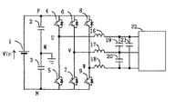
図1に本発明による運転方法が適用されるインバータ装置の実施例を示す。このインバータ装置は、逆並列ダイオードを有する半導体スイッチング素子4〜15、例えばIGBTを用いて直流電圧を交流電圧に変換する3相のインバータ装置であり、図3で既に説明した3レベルインバータと同じ回路構成を有する。従って、直流電源1に接続される直流入力端子P,N間には、第1および第2のコンデンサ2,3の直列接続回路が接続され、両コンデンサの共通接続点Mが、正負の直流入力端子P,Nの電位に対して中性点電位を形成している。
FIG. 1 shows an embodiment of an inverter device to which the operation method according to the present invention is applied. This inverter device is a three-phase inverter device that converts a DC voltage into an AC voltage using
さらに、コンデンサ直列接続回路2,3に対して並列に、それぞれ2つの半導体スイッチング素子から成る3つの直列接続回路4および5、6および7、8および9が接続され、これらの直列接続回路の中間接続点U,V,Wが3相の交流出力端子を成している。これの交流出力端子U,V,Wには、リアクトル16〜18とコンデンサ19〜2とから成る3相フィルタを介して負荷22が接続される。更に、3レベルレベルインバータとして動作可能にするために、各相端子U,V,Wと共通接続点Mとの間にそれぞれ双方向スイッチが接続されており、各双方向スイッチは、互いに逆直列接続された2つの逆並列ダイオードを有する半導体スイッチング素子10および11、12および13、14および15から成る。
Further, three
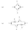
なお、各双方向スイッチとしては、図6(a)に示すように2つの半導体スイッチング素子Sを逆並列に接続して構成もの、また、図6(b)に示すように、2つの、直列にダイードDを接続した半導体スイッチング素子Sを逆並列に接続して構成したもの等を使用してもよい。 Each bidirectional switch has a configuration in which two semiconductor switching elements S are connected in antiparallel as shown in FIG. 6A, and two series switches as shown in FIG. 6B. A semiconductor switching element S connected to the diode D may be connected in reverse parallel.
インバータ装置の直流入力端子P,N間に接続される直流電源1は、条件によって電圧が大きく変動する直流電源、例えば太陽電池である。直流電源1から供給される直流入力電圧Vinを監視するために入力電圧検出部23が設けられている。入力電圧検出部23は、直流入力電圧Vinを検出し、その検出値を予め設定した規定値と比較し、その比較結果を出力するように構成されている。
The
入力電圧検出部23の出力信号は制御回路24に入力される。この制御回路24は、3相インバータブリッジを構成する半導体スイッチング素子4〜9および各双方向スイッチを構成する半導体スイッチング素子10〜15のPWM制御信号を生成する。この制御回路24は、インバータ装置を、図3において説明した如き3レベルインバータとして動作させる第1モードと、図2において説明した如き2レベルインバータとして動作させる第2モードとの2つの異なる制御動作モード間で切り替えが可能に構成されている。第1モードでは、インバータブリッジの各相の上下アームを成す第1および第2の半導体スイッチング素子4および5、6および7、8および9のみならず、双方向スイッチの半導体スイッチング素子10および11、12および13、14および15もスイッチングさせる。第2モードでは、双方向スイッチを構成する半導体スイッチング素子10および11、12および13、14および15をオフにして、第1および第2の半導体スイッチング素子4および5、6および7、8および9のみをスイッチングさせる。
An output signal from the
2つの異なる制御動作モード間の切り替えは、制御回路24に入力される入力電圧検出部23からの指令信号によって指令される。入力電圧検出部23は、制御回路24に対して、直流入力電圧Vinが規定値以上のときは、3レベルインバータ動作である第1モードを指令する信号を出力し、直流入力電圧Vinが規定値を以下のときは、2レベルインバータ動作である第2モードを指令する信号を出力する。
Switching between two different control operation modes is commanded by a command signal from the input
既に、図2〜4の説明から理解できるように、3レベルインバータは、サージ電圧によりスイッチング素子4〜9に過電圧が印加される恐れを回避するためには有利であるが、双方向スイッチを構成するスイッチング素子10〜15により導通損が増加するという欠点がある。一方、2レベルインバータは、双方向スイッチによる導通損の増加がないという点では有利であるが、サージ電圧によりスイッチング素子4〜9に過電圧が印加される恐れを回避するためには耐圧の大きい素子を使用しなければならず、この点では不利である。
As can be understood from the description of FIGS. 2 to 4, the three-level inverter is advantageous in order to avoid the possibility that an overvoltage is applied to the
本発明は、3レベルインバータ動作が可能なインバータ装置を用いて、3レベルインバータ動作と2レベルインバータ動作とを使い分けることによって、それぞれの長所を活かしながら、それぞれの欠点を除去しようとするものである。従って、本発明によれば、直流入力電圧Vinが規定値以上の高いレベルにあるときには、双方向スイッチを用いてインバータ装置を3レベルインバータとして動作させることにより、サージ電圧によるスイッチング素子への過電圧印加を回避する。そして、直流入力電圧Vinが規定値以下の低いレベルにあるときには、サージ電圧によるスイッチング素子への過電圧印加の恐れがないので、双方向スイッチをオフにして2レベルインバータとして動作させることによって双方向スイッチによる導通損の増加を回避する。それによって、インバータ装置の長時間の運用に対するトータルでの損失を抑制することができる。 The present invention intends to eliminate the respective disadvantages while utilizing the respective advantages by properly using the three-level inverter operation and the two-level inverter operation by using the inverter device capable of performing the three-level inverter operation. . Therefore, according to the present invention, when the DC input voltage Vin is at a level higher than the specified value, the inverter device is operated as a three-level inverter using a bidirectional switch, thereby applying an overvoltage to the switching element due to a surge voltage. To avoid. When the DC input voltage Vin is at a low level below the specified value, there is no risk of overvoltage being applied to the switching element due to surge voltage. Therefore, the bidirectional switch is operated by turning off the bidirectional switch and operating as a two-level inverter. Avoid increase in conduction loss due to. Thereby, the total loss for the long-time operation of the inverter device can be suppressed.
ところで上述のように直流電源1の電圧が大きくなるのは開放電圧付近であることが多い。太陽電池を例にとって説明すると、その電圧−電流特性は図5に示すとおりである。ハッチングを付けた部分の面積Sが出力電力に相当し、特性曲線上における最大面積をもたらす点が最大出力点Pmaxである。太陽電池の運転時には極力最大出力点Pmaxの付近で動作するように制御され、これが太陽電池発電装置の定格電力となる。一方、最大電圧付近では太陽電池の出力電流が小さくなる。入力電圧検出部23において規定値を適切に設定することによって、このような範囲の電圧に対してのみ、3レベルインバータ動作を行うならば、双方向スイッチは定格時に対して小さい電流しか流さないため、双方向スイッチを成すスイッチング素子10〜15の電流容量を小さくでき、インバータ装置の小形化、低価格化が実現できる。
Incidentally, as described above, the voltage of the
1 直流電源
2,3 コンデンサ
4〜9 第1および第2の半導体スイッチング素子
10〜15 第3および第4の半導体スイッチング素子
16〜21 交流フィルタ
22 負荷
23 入力電圧検出部
24 制御回路
DESCRIPTION OF
Claims (4)
直流入力電圧を検出し、検出した直流入力電圧が規定値以上のときは、第1および第2の半導体スイッチング素子のみならず双方向スイッチの半導体スイッチング素子もスイッチングさせることによりインバータ装置を3レベルインバータとして動作させ、検出した直流入力電圧が規定値以下のときは、双方向スイッチの半導体スイッチング素子をオフにして第1および第2の半導体スイッチング素子のみをスイッチングさせることによりインバータ装置を2レベルインバータとして動作させることを特徴とするインバータ装置の運転方法。 An inverter device using a semiconductor switching element having an anti-parallel diode, a series connection circuit including two capacitors between input terminals to which a DC input voltage fluctuating from a DC power supply is applied, and a first and a second At least one series connection circuit composed of semiconductor switching elements is connected in parallel, a common connection point of the first and second semiconductor switching elements is used as an AC output terminal, and between the AC output terminal and a common connection point of both capacitors In addition, in order to operate the inverter device formed by connecting the bidirectional switch composed of the third and fourth semiconductor switching elements connected in reverse series with each other,
When the DC input voltage is detected and the detected DC input voltage is equal to or higher than a specified value, the inverter device is switched to a three-level inverter by switching not only the first and second semiconductor switching elements but also the bidirectional switching semiconductor switching elements. When the detected DC input voltage is below the specified value, the bidirectional switching switch semiconductor switching element is turned off and only the first and second semiconductor switching elements are switched to make the inverter device a two-level inverter. An operation method of an inverter device, characterized by being operated.
直流入力電圧を検出し、検出した直流入力電圧が規定値以上のときは第1モードを指令する信号を出力し、検出した直流入力電圧が規定値以下のときは第2モードを指令する信号を出力する入力電圧検出部と、
インバータ装置を3レベルインバータとして動作させるべく第1および第2の半導体スイッチング素子のみならず第3および第4の半導体スイッチング素子もスイッチングさせる第1モードの制御信号と、インバータ装置を2レベルインバータとして動作させるべく第3および第4の半導体スイッチング素子をオフにして第1および第2の半導体スイッチング素子のみをスイッチングさせる第2モードの制御信号とを、前記電圧検出部から出力される前記第1モードを指令する信号または前記第2モードを指令する信号にしたがって選択的に出力する制御回路と、
を設けたことを特徴とするインバータ装置。 An inverter device using a semiconductor switching element having an anti-parallel diode, a series connection circuit including two capacitors between input terminals to which a DC input voltage fluctuating from a DC power supply is applied, and a first and a second At least one series connection circuit composed of semiconductor switching elements is connected in parallel, a common connection point of the first and second semiconductor switching elements is used as an AC output terminal, and between the AC output terminal and a common connection point of both capacitors In an inverter device formed by connecting a bidirectional switch composed of third and fourth semiconductor switching elements connected in reverse series with each other,
A DC input voltage is detected. When the detected DC input voltage is equal to or greater than a specified value, a signal for instructing the first mode is output. When the detected DC input voltage is equal to or less than a specified value, a signal for instructing the second mode is output. An input voltage detector to output;
A control signal in the first mode for switching not only the first and second semiconductor switching elements but also the third and fourth semiconductor switching elements to operate the inverter apparatus as a three-level inverter, and the inverter apparatus operates as a two-level inverter And a second mode control signal for switching only the first and second semiconductor switching elements by turning off the third and fourth semiconductor switching elements, and the first mode output from the voltage detector. A control circuit that selectively outputs in accordance with a signal to command or a signal to command the second mode;
An inverter device characterized by comprising:
Priority Applications (1)
| Application Number | Priority Date | Filing Date | Title |
|---|---|---|---|
| JP2012258552A JP2014107931A (en) | 2012-11-27 | 2012-11-27 | Method for operating inverter device, and inverter device |
Applications Claiming Priority (1)
| Application Number | Priority Date | Filing Date | Title |
|---|---|---|---|
| JP2012258552A JP2014107931A (en) | 2012-11-27 | 2012-11-27 | Method for operating inverter device, and inverter device |
Publications (1)
| Publication Number | Publication Date |
|---|---|
| JP2014107931A true JP2014107931A (en) | 2014-06-09 |
Family
ID=51028995
Family Applications (1)
| Application Number | Title | Priority Date | Filing Date |
|---|---|---|---|
| JP2012258552A Pending JP2014107931A (en) | 2012-11-27 | 2012-11-27 | Method for operating inverter device, and inverter device |
Country Status (1)
| Country | Link |
|---|---|
| JP (1) | JP2014107931A (en) |
Cited By (4)
| Publication number | Priority date | Publication date | Assignee | Title |
|---|---|---|---|---|
| JP2016226272A (en) * | 2015-05-27 | 2016-12-28 | ▲陽▼光▲電▼源股▲分▼有限公司Sungrow Power Supply Co., Ltd. | Pre-charge circuit and photovoltaic inverter |
| JP2017093039A (en) * | 2015-11-04 | 2017-05-25 | 株式会社日立製作所 | Power converter and control method |
| US10523049B2 (en) * | 2014-12-25 | 2019-12-31 | Toshiba Mitsubishi-Electric Industrial Systems Corporation | Uninterruptible power supply apparatus |
| WO2023272512A1 (en) * | 2021-06-29 | 2023-01-05 | 西门子股份公司 | Switching control method for three-level flying-capacitor converter |
Citations (4)
| Publication number | Priority date | Publication date | Assignee | Title |
|---|---|---|---|---|
| JP2002247862A (en) * | 2001-02-20 | 2002-08-30 | Hitachi Ltd | Power converter |
| JP2003169480A (en) * | 2001-11-30 | 2003-06-13 | Toshiba Corp | Control apparatus for neutral point clamp system power converter |
| JP2011254672A (en) * | 2010-06-04 | 2011-12-15 | Fuji Electric Co Ltd | Power semiconductor module and power conversion device using the same |
| WO2012025978A1 (en) * | 2010-08-23 | 2012-03-01 | 東芝三菱電機産業システム株式会社 | Electricity conversion device |
-
2012
- 2012-11-27 JP JP2012258552A patent/JP2014107931A/en active Pending
Patent Citations (4)
| Publication number | Priority date | Publication date | Assignee | Title |
|---|---|---|---|---|
| JP2002247862A (en) * | 2001-02-20 | 2002-08-30 | Hitachi Ltd | Power converter |
| JP2003169480A (en) * | 2001-11-30 | 2003-06-13 | Toshiba Corp | Control apparatus for neutral point clamp system power converter |
| JP2011254672A (en) * | 2010-06-04 | 2011-12-15 | Fuji Electric Co Ltd | Power semiconductor module and power conversion device using the same |
| WO2012025978A1 (en) * | 2010-08-23 | 2012-03-01 | 東芝三菱電機産業システム株式会社 | Electricity conversion device |
Cited By (5)
| Publication number | Priority date | Publication date | Assignee | Title |
|---|---|---|---|---|
| US10523049B2 (en) * | 2014-12-25 | 2019-12-31 | Toshiba Mitsubishi-Electric Industrial Systems Corporation | Uninterruptible power supply apparatus |
| JP2016226272A (en) * | 2015-05-27 | 2016-12-28 | ▲陽▼光▲電▼源股▲分▼有限公司Sungrow Power Supply Co., Ltd. | Pre-charge circuit and photovoltaic inverter |
| US9912252B2 (en) | 2015-05-27 | 2018-03-06 | Sungrow Power Supply Co., Ltd. | Pre-charge circuit and photovoltaic inverter |
| JP2017093039A (en) * | 2015-11-04 | 2017-05-25 | 株式会社日立製作所 | Power converter and control method |
| WO2023272512A1 (en) * | 2021-06-29 | 2023-01-05 | 西门子股份公司 | Switching control method for three-level flying-capacitor converter |
Similar Documents
| Publication | Publication Date | Title |
|---|---|---|
| JP6227041B2 (en) | Multi-level inverter | |
| US8811048B2 (en) | Medium voltage variable frequency driving system | |
| US9450502B2 (en) | Direct power conversion device and method for controlling direct power conversion device | |
| JP5995139B2 (en) | Bidirectional DC / DC converter | |
| JP6206502B2 (en) | Power conversion device and power conversion method | |
| US10003273B2 (en) | Power conversion device | |
| US10038392B2 (en) | Inverter | |
| CN109769404B (en) | System interconnection inverter device and method for operating the same | |
| JP2013219903A (en) | Rectifier circuit | |
| US9397581B2 (en) | Power conversion apparatus that provides a release path for inductive energy accumulated in an inductive load | |
| JP2011147233A (en) | Z source boost circuit | |
| JP2011188655A (en) | Dc-ac power conversion controller | |
| JP2018007403A (en) | Power converter | |
| US8787055B2 (en) | Inverter device | |
| JP5919483B2 (en) | Grid interconnection device | |
| JP5362657B2 (en) | Power converter | |
| JP2014107931A (en) | Method for operating inverter device, and inverter device | |
| JP6142926B2 (en) | Power converter | |
| JP5805059B2 (en) | Power converter | |
| JPWO2012098709A1 (en) | Power converter | |
| US20140301119A1 (en) | Multilevel AC/DC Power Converting Method and Converter Device Thereof | |
| JP2019161892A (en) | Power conditioner | |
| JP6516182B2 (en) | Power converter circuit and power converter using the same | |
| JP2016127677A (en) | Power converter | |
| JPWO2014167719A1 (en) | Power conversion apparatus, motor drive apparatus including the same, blower including the same, compressor, air conditioner including them, refrigerator, and refrigerator |
Legal Events
| Date | Code | Title | Description |
|---|---|---|---|
| A621 | Written request for application examination |
Free format text: JAPANESE INTERMEDIATE CODE: A621 Effective date: 20151014 |
|
| A977 | Report on retrieval |
Free format text: JAPANESE INTERMEDIATE CODE: A971007 Effective date: 20160727 |
|
| A131 | Notification of reasons for refusal |
Free format text: JAPANESE INTERMEDIATE CODE: A131 Effective date: 20160809 |
|
| A521 | Request for written amendment filed |
Free format text: JAPANESE INTERMEDIATE CODE: A523 Effective date: 20160926 |
|
| A02 | Decision of refusal |
Free format text: JAPANESE INTERMEDIATE CODE: A02 Effective date: 20170207 |