EP2291906B1 - Inverter and method for operating the inverter - Google Patents
Inverter and method for operating the inverter Download PDFInfo
- Publication number
- EP2291906B1 EP2291906B1 EP09769079.6A EP09769079A EP2291906B1 EP 2291906 B1 EP2291906 B1 EP 2291906B1 EP 09769079 A EP09769079 A EP 09769079A EP 2291906 B1 EP2291906 B1 EP 2291906B1
- Authority
- EP
- European Patent Office
- Prior art keywords
- freewheeling
- diode
- resonant
- semiconductor switch
- capacitor
- Prior art date
- Legal status (The legal status is an assumption and is not a legal conclusion. Google has not performed a legal analysis and makes no representation as to the accuracy of the status listed.)
- Not-in-force
Links
Images


Classifications
-
- H—ELECTRICITY
- H02—GENERATION; CONVERSION OR DISTRIBUTION OF ELECTRIC POWER
- H02M—APPARATUS FOR CONVERSION BETWEEN AC AND AC, BETWEEN AC AND DC, OR BETWEEN DC AND DC, AND FOR USE WITH MAINS OR SIMILAR POWER SUPPLY SYSTEMS; CONVERSION OF DC OR AC INPUT POWER INTO SURGE OUTPUT POWER; CONTROL OR REGULATION THEREOF
- H02M1/00—Details of apparatus for conversion
- H02M1/32—Means for protecting converters other than automatic disconnection
- H02M1/34—Snubber circuits
-
- H—ELECTRICITY
- H02—GENERATION; CONVERSION OR DISTRIBUTION OF ELECTRIC POWER
- H02M—APPARATUS FOR CONVERSION BETWEEN AC AND AC, BETWEEN AC AND DC, OR BETWEEN DC AND DC, AND FOR USE WITH MAINS OR SIMILAR POWER SUPPLY SYSTEMS; CONVERSION OF DC OR AC INPUT POWER INTO SURGE OUTPUT POWER; CONTROL OR REGULATION THEREOF
- H02M7/00—Conversion of ac power input into dc power output; Conversion of dc power input into ac power output
- H02M7/42—Conversion of dc power input into ac power output without possibility of reversal
- H02M7/44—Conversion of dc power input into ac power output without possibility of reversal by static converters
- H02M7/48—Conversion of dc power input into ac power output without possibility of reversal by static converters using discharge tubes with control electrode or semiconductor devices with control electrode
- H02M7/53—Conversion of dc power input into ac power output without possibility of reversal by static converters using discharge tubes with control electrode or semiconductor devices with control electrode using devices of a triode or transistor type requiring continuous application of a control signal
- H02M7/537—Conversion of dc power input into ac power output without possibility of reversal by static converters using discharge tubes with control electrode or semiconductor devices with control electrode using devices of a triode or transistor type requiring continuous application of a control signal using semiconductor devices only, e.g. single switched pulse inverters
- H02M7/5387—Conversion of dc power input into ac power output without possibility of reversal by static converters using discharge tubes with control electrode or semiconductor devices with control electrode using devices of a triode or transistor type requiring continuous application of a control signal using semiconductor devices only, e.g. single switched pulse inverters in a bridge configuration
-
- H—ELECTRICITY
- H02—GENERATION; CONVERSION OR DISTRIBUTION OF ELECTRIC POWER
- H02M—APPARATUS FOR CONVERSION BETWEEN AC AND AC, BETWEEN AC AND DC, OR BETWEEN DC AND DC, AND FOR USE WITH MAINS OR SIMILAR POWER SUPPLY SYSTEMS; CONVERSION OF DC OR AC INPUT POWER INTO SURGE OUTPUT POWER; CONTROL OR REGULATION THEREOF
- H02M1/00—Details of apparatus for conversion
- H02M1/32—Means for protecting converters other than automatic disconnection
- H02M1/34—Snubber circuits
- H02M1/346—Passive non-dissipative snubbers
-
- Y—GENERAL TAGGING OF NEW TECHNOLOGICAL DEVELOPMENTS; GENERAL TAGGING OF CROSS-SECTIONAL TECHNOLOGIES SPANNING OVER SEVERAL SECTIONS OF THE IPC; TECHNICAL SUBJECTS COVERED BY FORMER USPC CROSS-REFERENCE ART COLLECTIONS [XRACs] AND DIGESTS
- Y02—TECHNOLOGIES OR APPLICATIONS FOR MITIGATION OR ADAPTATION AGAINST CLIMATE CHANGE
- Y02B—CLIMATE CHANGE MITIGATION TECHNOLOGIES RELATED TO BUILDINGS, e.g. HOUSING, HOUSE APPLIANCES OR RELATED END-USER APPLICATIONS
- Y02B70/00—Technologies for an efficient end-user side electric power management and consumption
- Y02B70/10—Technologies improving the efficiency by using switched-mode power supplies [SMPS], i.e. efficient power electronics conversion e.g. power factor correction or reduction of losses in power supplies or efficient standby modes
Definitions
- the invention relates to an inverter for converting an input-side DC voltage into an output-side AC voltage comprising an H-bridge with four semiconductor switches, wherein at least one semiconductor switch clocks, wherein further between the H-bridge and output side AC voltage terminals, a storage inductor is provided and wherein the storage inductor a Freewheeling path with a freewheeling diode for commutation of the current after a shutdown of a semiconductor switch of the H-bridge comprises. Furthermore, the invention relates to a method for operating the inverter.
- inverter topologies are known.
- a very common feature is the so-called H-bridge.
- Four semiconductor switches, in particular IGBTs, are arranged in a bridge circuit.
- the triggering of the clocking semiconductor switch is usually carried out by means of pulse width modulation for simulating a sinusoidal voltage waveform of a connected AC voltage network, the clock frequency is a multiple of the mains frequency.
- Such an inverter topology is from the US-A-4937725 known.
- Inverters are increasingly being used to feed energy from alternative energy sources, such as solar generators or fuel cells, into public AC grids or island grids. To make this form of energy production economical, all components must have a high efficiency. This applies in particular to inverters for network-synchronous conversion of the energy obtained.
- Zero voltage switching (ZVS) and zero current switching (ZCS) are known.
- Another source of power losses represent the freewheeling phases after switching off a semiconductor switch. These arise through the output side arranged inductor circuits whose inductor current continues to flow when the semiconductor switch is turned off. Freewheeling paths within an inverter circuit are usually via parasitic diodes of the semiconductor switches or via dedicated freewheeling diodes. Since a voltage is applied to these diodes usually at the beginning of a freewheeling phase, arise during the rise of the current through the diodes, a power loss that limits the efficiency of the inverter to the top.
- the invention has the object of developing the known from the prior art inverter to achieve improved efficiency.
- each clocking semiconductor switch is coupled to the zero voltage switching to a resonant circuit comprising capacitive resonant elements and inductive resonant elements
- the freewheeling path comprises a first and a second freewheeling diode in parallel
- said parallel circuit in Series is connected to the inductive resonant elements
- the second freewheeling diode is connected in series with capacitive freewheeling elements which as elements of the resonant circuit at the beginning of a freewheeling phase for zero voltage switching of the second freewheeling diode to a corresponding voltage charged.
- the energy stored in the resonant circuit during a turn-off phase is used to charge the capacitive freewheeling elements in a switch-on phase of the clocking semiconductor switch.
- the freewheeling elements are connected in series with the second freewheeling diode in order to de-energize them at the beginning of a freewheeling phase.
- the capacitive freewheeling elements discharge in a first period of the freewheel, wherein the first freewheeling diode is de-energized and commutes the freewheeling current without losses to the first freewheeling diode.
- the circuit according to claim 1 thus enables on the one hand a lossless switching of the semiconductor switch of the H-bridge and on the other hand a nearly lossless freewheel after switching off the clocking semiconductor switch.
- each resonant circuit comprises a resonant capacitor and a resonant choke, wherein a freewheeling capacitor is connected via coupling elements with a resonant capacitor and wherein a first branch of the freewheeling path comprises the first freewheeling diode and the resonant choke connected in series and wherein a second branch of the freewheeling path second freewheeling diode, the resonance choke and the freewheeling capacitor in series circuit comprises.
- the coupling elements are formed, for example, by diode circuits for determining a corresponding current direction during a resonant oscillation or by transformers. Over the coupling elements energy is thus transferred from the resonant capacitor to the freewheeling capacitor after a turn-on of the clocking semiconductor switch to ensure a power-free freewheel for the next shutdown.
- the freewheeling path comprises a further H-bridge with four auxiliary semiconductor switches, the first auxiliary semiconductor switch of the further H-bridge being connected via the first storage inductor and the third auxiliary semiconductor switch of the further H-bridge being connected via the second storage inductor to the first AC voltage terminal and the second Auxiliary semiconductor switch of the further H-bridge via the third storage inductor and the fourth auxiliary semiconductor switch of the further H-bridge via the fourth storage inductor are connected to the second AC voltage terminal.
- Such a connection of the H-bridge and the further H-bridge via four storage chokes to the two AC voltage connections has the advantage that both during a positive and during a negative half cycle of the AC voltage, a freewheeling path is available without the use of the parasitic diodes in the auxiliary semiconductor switches , This avoids losses that would otherwise be caused during a freewheeling by the usually slow parasitic diodes.
- connection of the third and the fourth auxiliary semiconductor switch and the connection of the first and the second auxiliary semiconductor switch via a series circuit of the first freewheeling diode and a resonance choke are connected in parallel to the first free-wheeling diode series connection is arranged from the second freewheeling diode and freewheeling capacitor, that further comprises a connection point between the second freewheeling diode and freewheeling capacitor via a Series circuit of a third diode and a fourth diode is connected to the connection of the first and the second auxiliary semiconductor switch, that in parallel to the third diode, a secondary winding of a transformer is arranged, which also comprises two primary windings, wherein the first primary winding with one end to the compound of is connected to the other end via a first resonant capacitor to the connection between the first semiconductor switch and the first storage inductor and a second resonant capacitor to the connection between the second semiconductor switch and the third storage inductor and wherein the second
- one half of the H-bridge is connected via a first storage inductor to a first AC voltage terminal and the other half of the H-bridge is connected to a second AC voltage terminal via a second storage inductor.
- the freewheeling path comprises a further H-bridge with four auxiliary semiconductor switches, wherein one half of the further H-bridge is connected to the first AC voltage connection via the first storage inductor and the other half of the further H-bridge is connected via the second storage inductor to the second VLC voltage connection is switched.
- Such a circuit with only two storage chokes at the inverter outputs is useful when the auxiliary semiconductor switches have fast parasitic diodes, whereby the losses during the freewheel small being held.
- the first and fourth semiconductor switches clock during a positive half cycle, and the second and third semiconductor switches during a negative half cycle.
- a circuit supplement is advantageous in which the connection of the third and the fourth auxiliary semiconductor switch and the connection of the first and the second auxiliary semiconductor switch via a series circuit of a second resonance choke, the first free-wheeling diode and a first Resonance choke are connected, and in parallel to the first freewheeling diode, a series circuit of a second freewheeling capacitor, the second freewheeling diode and a first freewheeling capacitor is arranged.
- connection point between the second freewheeling diode and the first freewheeling capacitor via a series circuit of a third diode and a fourth diode connected to the connection of the first and second auxiliary semiconductor switch and the connection of the third and the fourth auxiliary semiconductor switch via a sixth diode and a fifth diode with a connection point between the second freewheeling diode and the second freewheeling capacitor connected.
- a connection point between third and fourth diode via a first resonant capacitor to the connection of the first semiconductor switch and the second semiconductor switch and a connection point between the fifth and sixth diode via a second resonant capacitor connected to the compound of the third semiconductor switch and the fourth semiconductor switch.
- simple diode circuits are arranged as coupling elements between the resonance capacitors, the resonance chokes and the freewheeling capacitors.
- the Current flows between these devices flow during a clock cycle in such a way that the diodes in these diode circuits as well as the free-wheeling diodes become conductive without loss.
- One clock cycle is determined by a switch-on of a clocking semiconductor switch to the next power-on.
- the first resonant circuit which comprises the first resonant capacitor, the first freewheeling capacitor and the first resonant choke
- the second resonant circuit which comprises the second resonant capacitor, the second freewheeling capacitor and the second resonant choke, serves for the zero voltage switching of the third and the fourth semiconductor switch.
- the resonance capacitors are charged to almost half the input side DC voltage before a switch-on.
- a further embodiment of the invention provides that a first H-bridge connection between the first semiconductor switch and the fourth semiconductor switch is connected via a first storage choke to a first AC voltage terminal and a second H-bridge connection between the second semiconductor switch and the third semiconductor switch via a second storage choke with a second Furthermore, the connection of the third and the fourth semiconductor switch via a series circuit of the first freewheeling diode and the first resonant choke are connected to the first H-bridge connection that parallel to the first freewheeling diode a series circuit of the second freewheeling diode and the first freewheeling capacitor is arranged, that parallel to the first semiconductor switch, a series circuit of a first reson capacitor and a fourth diode is arranged and that a connection point between the second Freewheeling diode and first freewheeling capacitor is connected via a third diode to a connection point between the first resonant capacitor and the fourth diode, further that the connection of the third and the fourth semiconductor switch via a series circuit of another first freewheeling diode and second
- This embodiment is thus designed as an inverter with mains transformer.
- only one semiconductor switch clocks namely only the first semiconductor switch during a positive half-cycle; the third semiconductor switch is always on and the second and fourth semiconductor switches are always off.
- the second semiconductor switch clocks and the fourth semiconductor switch is always on; the first and third semiconductor switches are always off.
- the DC voltage connections are connected to one another via an input capacitor. This is especially appropriate if the input side in the Power fluctuating power source is connected, such as a solar generator.
- the AC voltage connections are connected to one another via an output capacitor.
- a method for operating one of the inverters described above provides that at the beginning of a clock cycle at least one semiconductor switch of the H-bridge is turned on, that while the input-side DC voltage is drawn to the inductive resonant elements of the respective resonant circuit, whereby the still as a freewheeling current through the inductive Resonance elements flowing current decreases and reverses its direction and that subsequently by means of this current energy is transferred from the capacitive resonance elements to the capacitive freewheeling elements, that after a predetermined switch-on the at least one clocking semiconductor switch is switched off again and at least a portion of the freewheeling current through the second freewheeling diode, the capacitive freewheeling elements and the inductive resonance elements flows until the capacitive freewheeling elements are discharged and the remaining freewheeling current through the first freewheeling diode and the inductive Reso nanzetti flows.
- This is a passive, low-loss method for reducing the switching losses of semiconductors, in particular IGBTs, specified as an H-
- a first embodiment of the invention is in Fig. 1 shown.
- the H-bridge is equipped with four semiconductor switches S1, S2, S3, S4 Input side to an energy source 1, for example, a power source, a voltage source or a non-linear source (solar generator) connected.
- An input capacitor Cin buffers the energy in a given voltage range.
- the first semiconductor switch S1 is connected via a first storage inductor L1 and the third semiconductor switch S3 is connected via a second storage inductor L2 to a first AC voltage connection.
- the second semiconductor switch S2 is connected via a third storage inductor L3 and the fourth semiconductor switch S4 is connected via a fourth storage inductor L4 to a second AC voltage connection.
- a consumer network 2 is connected to the two inverter connections. In this case, an output capacitor Co ensures a smoothing of the current fed into the consumer network 2.
- a further H-bridge with four auxiliary semiconductor switches HS1, HS2, HS3, HS4 is arranged.
- These auxiliary semiconductor switches HS1, HS2, HS3, HS4 are connected in parallel to the semiconductor switches S1, S2, S3, S4 of the first H-bridge to the four storage inductors L1, L2, L3, L4.
- the counting of the semiconductor switches S1, S2, S3, S4 and the auxiliary semiconductor switches HS1, HS2, HS3, HS4 takes place in the usual manner for an H-bridge representation in a clockwise direction.
- the semiconductor switches S1, S2, S3, S4 and Hilfshalbeiterschalter HS1, HS2, HS3, HS4 are formed for example as IGBTs. In Fig. 1 they are shown as such, each with a parasitic diode (body diode).
- a double resonance circuit is arranged.
- one side of a first resonance choke RL1 is connected to the cathode of a fourth diode D4.
- the anode of this fourth diode D4 is connected via a first resonant capacitor RC1 to the Bridge connection of the first and second semiconductor switches S1, S2 connected.
- this one side of the first resonance choke RL1 is connected to the bridge connection of the first and the second auxiliary semiconductor switch HS1, HS2.
- the other side of the first resonant choke RL1 is connected to the cathode of a first freewheeling diode D1 and also connected via a first freewheeling capacitor FC1 on the one hand to the cathode of a second freewheeling diode D2 and on the other hand via a third diode D3 to a connection point between the first resonant capacitor RC1 and fourth diode D4 ,
- the third diode D3 is switched from the first freewheeling capacitor FC1 to the first resonance capacitor RC1 in the forward direction.
- a second resonant capacitor RL2 is connected via a sixth diode D6 and a second resonant capacitor RC2 to the bridge connection between third and fourth semiconductor switches S3, S4.
- the sixth diode D6 is arranged from the second resonant choke RL2 to the second resonant capacitor RC2 in the forward direction.
- This one side of the second resonant choke RL2 is also connected to the bridge connection between the third and fourth auxiliary semiconductor switches HS3, HS4.
- the other side of the second resonant choke RL2 is connected on the one hand to the anode of the first filament diode D1 and on the other hand via a second freewheeling capacitor FC2 to the anode of the second freewheeling diode D2.
- a fifth diode D5 is arranged in the forward direction from the second resonance capacitor RC2 to the second free-running capacitor FC2.
- the main circuit consists of an H-bridge whose semiconductor switches S1, S2, S3, S4 are switched by means of a controller with a predetermined clock frequency.
- the auxiliary switching elements HS1, HS2, HS3, HS4 are switched on and off by means of control with a predetermined mains frequency (for example 50 Hz).
- the clock frequency exceeds the mains frequency by a multiple.
- the circuit allows the freewheeling current of the storage chokes L1, L2, L3, L4, after turning off the semiconductor switches S1, S4 during a positive half-wave and S2, S3 during a negative half cycle, only as rectifier diode D1 and not by the slower switching parasitic diodes the auxiliary semiconductor switch HS1, HS2, HS3, HS4 to flow.
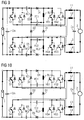
- FIGS. 3 and 4 the switching phases are shown during a positive half cycle of the output alternating current.
- the first and fourth semiconductor switches S1, S4 are switched at the clock frequency, the second and third semiconductor switches S2, S3 remain off.
- the first and the fourth auxiliary semiconductor switches HS1, HS4 are always switched on during a positive half-cycle, the two other auxiliary semiconductor switches HS2, HS3 are either switched off or clocked inverting to the clocking semiconductor switches S1, S4 of the first H-bridge.
- the first and fourth semiconductor switches S1, S4 are turned on.
- the current flows from the power source 1 coming through the first semiconductor switch S1, the first storage inductor L1, a connected network 2 and further via the fourth storage inductor L4 and the fourth semiconductor switch S4 back to the power source.
- the first and fourth semiconductor switches S1, S4 are turned off.
- the freewheeling current of the first and the fourth storage inductor L1, L4 flows through the free-wheeling diode D1, the first and the fourth auxiliary semiconductor switches HS1, HS4 and via the network 2.
- Analog to the switching phases during a positive half cycle are in the FIGS. 5 and 6 the switching phases during a negative half wave are shown.
- the first and the fourth semiconductor switches S1, S4 are always switched off during a negative half-cycle.
- the second and third semiconductor switches S2, S3 clock at the clock frequency.
- the first and fourth auxiliary semiconductor switches HS1, HS4 are either switched off or clocked in inverting to the clocking semiconductor switches S2, S3 of the first H-bridge.
- the other two auxiliary semiconductor switches HS2, HS3 are always switched on during a negative half-wave.
- a switch-on phase flows from the power source 1 coming through the second semiconductor switch S2, the third storage inductor L3, the connected network 2 and the second storage inductor L2 and the third semiconductor switch S3 back to the power source.
- the second and third semiconductor switches S2, S3 are turned off.
- the freewheeling current of the second and third storage inductor L2, L3 flows through the freewheeling diode D1 and also through the second and third auxiliary semiconductor switches HS2, HS3 and via the network 2.
- one clock cycle (a sequence of a switch-on phase and a switch-off phase) is subdivided into a plurality of time sections.
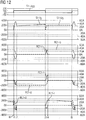
- FIGS. 7 to 11 is the embodiment described above with resonant circuits ( Fig. 1 ), wherein the current flows occurring in individual periods are plotted during a positive half cycle.
- the corresponding current and voltage curves over time are in the FIGS. 12 to 14 shown.
- One clock cycle begins at the turn-on time t0 with the on-switch of the first and fourth semiconductor switches S1, S4. It is assumed that, shortly before switching on, the freewheeling current of the first and fourth storage inductors L1, L4 flows through the first freewheeling diode D1 via the first and fourth auxiliary semiconductor switches HS1, HS4 and the first and second resonance inductors RL1, RL2. Furthermore, the first resonant capacitor RC1 is charged to almost half the voltage of the input capacitor Cin (or half the voltage of a solar generator connected, for example, on the input side), the negative potential of the first resonant capacitor RC1 being at the anode of the fourth diode D4.
- the second resonant capacitor RC2 is also charged to half the voltage of the input capacitor Cin (or half the voltage of a solar generator, for example, on the input side), its positive potential being at the cathode of the sixth diode D6 ( Fig. 7 ).
- a first time interval t0-t1 is in Fig. 8 shown.
- the first and fourth semiconductor switches S1, S4 are turned on.
- the current from the input-side power source 1 flows through the first and fourth semiconductor switches S1, S4 through the first and fourth storage inductors L1, L4.
- With the power switch of the first Semiconductor switch S1 is also a first resonant circuit, consisting of the first resonant capacitor RC1, the first resonant choke RL1 and the first freewheeling capacitor FC1 activated.
- a second resonant circuit consisting of the second resonant capacitor RC2, the second resonant choke RL2 and the second freewheeling capacitor FC2, which is activated by turning on the fourth semiconductor switch S4.
- the potential at the emitter of the first auxiliary semiconductor switch HS1 goes up massively, while the first resonance choke RL1 reduces its stored energy by driving its current into a very high voltage (the two resonance chokes RL1, RL2 are to a certain extent at the input side voltage). After a very short time, these two inductors RL1, RL2 have built up their magnetic field. As a result, the free-wheeling current in the first freewheeling diode D1 approaches zero via the two resonance chokes RL1, RL2.
- FIG. 12 shows the uppermost diagram shows the gate-source voltage S1-U GD at the first semiconductor switch S1.
- Fig. 12 below the course of the drain current S1-I D and the drain voltage S1-U D of the first semiconductor switch S1 is shown in a diagram. It follows from top to bottom a diagram with the current RC1-I and the voltage RC1-U of the first resonant capacitor RC1 over time, a graph with the current FC1-I and the voltage FC1-U of the first free-wheeling capacitor FC1 over time and a diagram with the current RL1-I and the voltage RL1-U of the first resonant choke RL1 over time.
- Fig. 13 shows from top to bottom the current D1-I and the voltage D1-U of the first freewheeling diode D1, the current D2-I and the voltage D2-U of the second freewheeling diode D2, the current D3-I and the voltage D3-U of the third Diode D3 and the current D4-I and the voltage D4-U of the fourth diode D4.
- Fig. 14 is finally from top to bottom a diagram with the current S1-I through the first semiconductor switch S1 and with the input current I in over time, a diagram with the current L1-I in the first storage inductor L1 (output current) and the current HS1- I through the first auxiliary semiconductor switch HS1 over time, a diagram with the current BDHS1-I through the parasitic diode of the first auxiliary semiconductor switch HS1 and the current HS1-I through the first auxiliary semiconductor switch HS1 over time and a diagram with the current BDSH2-I through the parasitic diode of the second auxiliary semiconductor switch HS2 and with the current L1-I in the first storage inductor L1 over time.
- the charge of the first resonant capacitor RC1 oscillates with a half cycle of the resonant frequency to the first free-wheel capacitor FC1. This is done by a current flow through the first semiconductor switch S1, the parasitic diode of the first auxiliary semiconductor switch HS1, the first resonant choke RL1 and the third diode D3.
- the charge of the second resonant capacitor RC2 oscillates with a half cycle of the resonant frequency to the second freewheeling capacitor FC2, wherein in this case the current through the fourth semiconductor switch S4, the fifth diode D5, the second resonant inductor RL2 and the parasitic diode of the fourth auxiliary semiconductor switch HS4 flows.
- the first freewheeling diode D1 switches off with zero voltage and the third and the fifth diode D3, D5 are turned on with zero voltage. Accordingly, no power loss is lost at these diodes.
- the charges of the resonance capacitors RC1, RC2 are completely transferred to the freewheeling capacitors FC1, FC2.
- the third diode D3 as well as the fifth diode D5 switches off with zero current and prevents further oscillation in the resonant circuits RC1, FC1, RL1 or RC2, FC2, RL2.
- the current from the power source 1 continues to flow in the first and fourth storage inductors L1, L4 via the first and fourth semiconductor switches S1, S4.
- the first and fourth semiconductor switches S1, S4 are turned off by means of a corresponding control (eg according to the pulse width modulation method).
- the current from the energy source 1 continues to flow via a parallel branch, namely, via the resonance capacitors RC1, RC2, via the fourth and sixth diodes D4, D6 and via the first and fourth auxiliary semiconductor switches HS1, HS4.
- the resonant capacitors RC1, RC2 are charged very quickly by the current in the storage chokes L1, L4.
- the freewheeling capacitors FC1, FC2 release their charge via the second free-wheeling diode D2, the resonance chokes RL1, RL2, the first and the fourth auxiliary semiconductor switches HS1, HS4 and the storage chokes L1, L4 to the connected network 2.
- the freewheeling capacitors FC1, FC2 are completely discharged.
- t4-t5 takes over again the first freewheeling diode D1, the freewheeling current.
- the same description sequence applies to the second and third semiconductor switches S2, S3 as clocking switches and to the second and third auxiliary semiconductor switch HS2, HS3 as an activated switch of the freewheel.
- the current flows through the second and the third storage inductor L2, L3.
- a resonance circuit with a transformer T is provided as a coupling element.
- a resonant choke RL is first connected in series with the first freewheeling diode D1.
- Parallel to the first freewheeling diode D1, the second freewheeling diode D2 is arranged in series with a freewheeling capacitor FC.
- a connection point between the second freewheeling diode D2 and freewheeling capacitor is connected via a third and a fourth diode D3, D4 to the bridge connection between the first and second auxiliary semiconductor switches HS1, HS2.
- a secondary winding of the transformer T is arranged parallel to the third diode, wherein the winding start of the secondary winding to the cathode of the third diode D3 and the anode of the fourth diode D4 is connected.
- the winding end is connected to the cathode of the second freewheeling diode D2 and one side of the freewheeling capacitor FC.
- the first primary winding is connected to the winding start on the one hand via a first resonant capacitor RC1 with a connection between the first semiconductor switch S1 and first storage inductor L1 and the other via a second resonant capacitor RC2 with a connection between the second semiconductor switch S2 and third storage inductor L3.
- the winding end of the first primary winding is connected to the bridge connection between the first and second semiconductor switches S1, S2.
- the winding start of the second primary winding to the bridge connection between the third and fourth semiconductor switch 53, S4 and the winding end of the second primary winding is connected on the one hand via a third resonant capacitor RC3 with a connection between the third semiconductor switch S3 and second storage inductor L2 and the other via a fourth resonant capacitor RC4 with a connection between the fourth semiconductor switch S4 and fourth storage inductor L4.
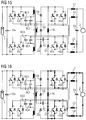
- FIGS. 16 to 20 show the current flows during a clock cycle in the previously defined periods t0-t1, t1-t2, t2-t3, t3-t4 and t4-t5 during a positive half cycle.
- the freewheeling current of the first and fourth storage inductors L1, L4 flows through the network, through the first and fourth auxiliary semiconductor switches, the first freewheeling diode D1 and the resonance inductor RL (FIG. Fig. 16 ).
- the charges of the second and the fourth resonant capacitor RC1, RC4 are transposed over the transformer T, the resonant choke RL and the fourth diode D4 onto the freewheeling capacitor FC ( Fig. 18 ).
- the fourth time interval t3-t4 introduced in this way is in Fig. 20 shown.
- current continues to flow from the energy source 1 via the first and the fourth resonance capacitor RC1, RC4 and the transformer T, which is in a flow phase, since the secondary diode D3 arranged on the secondary side is conductive. This happens until the two resonance capacitors RC1, RC4 are charged.
- the freewheeling capacitor FC discharges its charge to the network 2 via the second free-wheeling diode D2, the resonance choke RL and the first and the second auxiliary semiconductor switches HS1, HS4.
- the two resonance capacitors RC1, RC4 are fully charged and the current from the power source 1 goes to zero.
- the freewheeling capacitor FC is completely discharged and the freewheeling current commutates at zero voltage from the second freewheeling diode D2 to the first freewheeling diode D1.
- the illustrated embodiments of the invention have the advantage that all involved switching components (semiconductor switches and diodes) either at zero voltage or at zero current on or off. In this way, the switching losses of the inverter are reduced to a minimum.
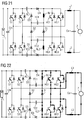
- the concept can be simplified by arranging only two storage inductors L1, L2 instead of the four storage inductors L1-L4 described so far at the output of the inverter are.
- the corresponding circuit is in Fig. 21 shown.
- Fig. 1 Opposite the circuit in Fig. 1 is here in the H-bridge of the first and fourth semiconductor switches S1, S4 connected to each other. Likewise, the second and third semiconductor switches S2, S3 are connected together. These connections are connected via a respective storage inductor L1, L2 to the AC voltage outputs. Parallel to this, the further H-bridge for the freewheel is arranged, wherein also here the first and the fourth auxiliary semiconductor switch HS1, HS4 and the second and the third auxiliary semiconductor switch HS2, HS3 are interconnected.
- the general switching conditions of such a circuit are as follows. During a positive half-cycle, the first and third semiconductor switches S1, S3 clock at the clock frequency, while the second and fourth semiconductor switches S2, S4 remain permanently switched off.
- the first and third auxiliary semiconductor switches HS1, HS3 are always turned on during a positive half-cycle, whereas the second and fourth auxiliary semiconductor switches HS2, HS4 are either turned off or clocked inversely to the semiconductor switches S1, S3.
- the second and fourth semiconductor switches S2, S4 and the first and third semiconductor switches S1, S3 remain switched off.
- the first and third auxiliary semiconductor switches HS1, HS3 are either switched off or clocked inverting the semiconductor switches S1, S3.
- the second and fourth auxiliary semiconductor switches HS2, HS4 are always turned on during a negative half cycle.
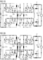
- HS4 is divided ( Fig. 22 . Fig. 27-29 ).
- the first resonant capacitor RC1 is charged with the half-cycle of the resonant frequency via the first semiconductor switch S1, the parasitic diode of the first auxiliary semiconductor switch HS1, the first resonant reactor RL1, and the third diode D3 first freewheeling capacitor FC1.
- the recharging of the second resonant capacitor RC2 to the second freewheeling capacitor FC2 via the fifth diode D5, the second resonant inductor RL2, the parasitic diode of the third auxiliary semiconductor switch HS3 and the third semiconductor switch S3 ( Fig. 24 . Fig. 27-29 ).
- the beginning of the fourth time interval t3-t4 is marked by the switching off of the first and third semiconductor switches S1, S3.
- the current from the power source 1 continues to flow through the resonance capacitors RC1 and RC2, via the fourth diode D4 and the sixth diode D6 and the first auxiliary semiconductor switch HS1 and the third auxiliary semiconductor switch HS3, respectively, until the two resonance capacitors RC1, RC2 are charged.
- the disconnecting capacitors FC1, FC2 give their charge via the second freewheeling diode D2, the first and third auxiliary semiconductor switches HS1, HS3 and the resonance chokes RL1, RL2 and the coil chokes L1, L2 to the network until they are completely discharged ( Fig. 26 . Fig. 27-29 )
- the resonance capacitors are fully charged and the current from the energy source 1 goes to zero.
- the freewheeling capacitors are completely discharged and the freewheeling current commutates at zero voltage from the second freewheeling diode D2 to the first freewheeling diode D1 and the parallel-connected parasitic or antiparallel diodes of the second and the fourth auxiliary semiconductor switch HS2, HS4.
- the freewheeling current flows divided into the first freewheeling diode D1 and the parallel-connected parasitic or antiparallel diodes of the second and fourth auxiliary semiconductor switches HS2, HS4 until the next switching-on process takes place ( Fig. 22 . Fig. 27-29 ).
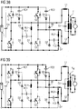
- Another embodiment of the present invention relates to an inverter with a mains transformer for galvanic isolation of the input side connected energy source 1 and the output side connected AC voltage network. 2
- An H-bridge with four semiconductor switches S1, S2, S3, S4 is as known on the input side to the power source 1 and the output side via two storage inductors L1, L2 connected to a primary winding of a power transformer T N. If necessary, an input capacitor Cin and, parallel to the primary winding, an output capacitor Co are on the input side arranged. Via a secondary winding of the power transformer T N , the connection to the network 2 ( Fig. 30 ).
- the clocking at the clock frequency semiconductor switches are switched unbalanced.
- the second and fourth semiconductor switches S2, S4 are always switched off, the third semiconductor switch S3 is always switched on and the first semiconductor switch S1 is clocked.
- the freewheeling current flows through the antiparallel or parasitic diode of the fourth semiconductor switch S4 and the switched-third semiconductor switch S3.
- the second semiconductor switch S2 clocks, the fourth semiconductor switch S4 always remains switched on and the first and third semiconductor switches S1, S3 always remain switched off.
- the freewheeling current flows here via the antiparallel or parasitic diode of the third semiconductor switch S3 and via the switched fourth semiconductor switch S4.
- the permanently switched semiconductor switches S3 and S4 and the clocking semiconductor switches S1 and S2 are reversed to be controlled. Accordingly, during a positive half cycle, the third semiconductor switch S3 can also be clocked and the first semiconductor switch S1 can be switched on permanently. During a negative half-cycle, the fourth semiconductor switch S4 can be clocked and the second semiconductor switch S2 can be switched on.
- Fig. 31 shows the design of the resonant circuit for an inverter with mains transformer.
- first semiconductor switch S1 form a first freewheeling diode D1, a third and fourth diode D3, D4, a first freewheeling capacitor FC1, a first resonant capacitor RC1 and a first freewheeling inductor RL1 a first resonant circuit.
- the first freewheeling diode D1 replaces the antiparallel or parasitic diode of the fourth semiconductor switch S4 in FIG Fig. 30 ,
- the first freewheeling diode D1 is connected with its anode to the bridge connection between the third and fourth semiconductor switches S3, S4.
- the cathode is connected via the first resonant choke RL1 to the bridge connection of the first and the fourth semiconductor switch S1, S4.
- Parallel to the first freewheeling diode D1, a second freewheeling diode D2 is connected in series with the first freewheeling capacitor FC1.
- the bridge connection of the first and second semiconductor switches S1, S2 is connected via the first resonance capacitor RC1 to the anode of the fourth diode D4, the cathode of which is connected to the bridge connection of the first and fourth semiconductor switches S1, S4.
- a connection point between the first resonant capacitor RC1 and the fourth diode D4 is connected to the cathode of the third diode D3 whose anode is connected to a connection point between the second freewheeling diode D2 and the first freewheeling capacitor FC1.
- the second semiconductor switch S2 form a further first freewheeling diode D1 ', a fifth and sixth diode D5, D6, a second freewheeling capacitor FC2, a second resonant capacitor RC2 and a second resonant choke RL2 a resonant circuit.
- This resonant circuit is arranged in the manner described above between the bridge connection of the second and third semiconductor switch S2, S3 and the bridge connection of the third and fourth semiconductor switch S3, S4, wherein parallel to the other first filament diode D1 'another second freewheeling diode D2' in series with the second freewheeling capacitor FC2 is provided.
- the freewheeling current flows in the storage inductors L1, L2 through the first filing diode D1, via the third semiconductor switch S3, the first resonant choke RL1 and via the mains transformer T N (FIG. Fig. 32 ).
- the first time interval t0-t1 starts to turn on the first semiconductor switch S1.
- the current from the power source 1 flows through the first semiconductor switch S1, through the storage chokes L1, L2, as well as the primary winding of the power transformer T N and via the third semiconductor switch S3.
- the charge of the first resonant capacitor RC1 oscillates with a half cycle of the resonant frequency to the first free-wheel capacitor FC1.
- the current flow in this case runs through the first semiconductor switch S1, the first resonant choke RL1 and via the third diode D3.
- the charge of the first resonance capacitor RC1 is completely transferred to the first free-wheeling capacitor FC1 and the third diode D3 turns off at zero current. This prevents further oscillation in the resonant circuit RC1, FC1, RL1.
- the current from the power source 1 continues to flow through the first and third semiconductor switches S1, S3, the storage chokes L1, L2 and the primary winding of the power transformer T N.
- the fourth time interval t3-t4 begins with the turning off of the first semiconductor switch S1.
- the third semiconductor switch S3 remains turned on. Through it, the current continues to flow from the power source 1 through the first resonance capacitor RC1, the fourth diode D4, via the storage chokes L1, L2, and the power transformer T N until the first resonance capacitor RC1 is charged.
- the first freewheeling capacitor FC1 discharges its charge via the first resonance choke RL1, the storage chokes L1, L2, the mains transformer T N , the third semiconductor switch S3 and the second freewheeling diode D2 to the network 2 until the first freewheeling capacitor FC1 is completely discharged.
- the first resonant capacitor RC1 is fully charged and the current from the power source 1 goes to zero.
- the first freewheeling capacitor FC1 is completely discharged and the freewheeling current commutates at zero voltage from the second one Freewheeling diode D2 to the first freewheeling diode D1.
- the freewheeling current of the storage inductors L1, L2 flows through the first freewheeling diode D1, via the third semiconductor switch S3, the first resonant inductor RL1 and the primary winding of the power transformer T N , until the first semiconductor switch S1 is turned on again.
- the second semiconductor switch S2 is turned on and the current from the power source 1 flows through this through the storage chokes L1, L2, the primary winding and the permanently switched fourth semiconductor switch S4.
- the charge of the second resonant capacitor RC2 oscillates with a half cycle of the resonant frequency to the second freewheeling capacitor FC2.
- the current flow in this case runs via the sixth diode D6, the second semiconductor switch S2 and the second resonant choke RL2.
- the charge of the second resonant capacitor RC2 is completely transferred to the second flywheel capacitor FC2.
- the sixth diode D6 turns off with zero current and prevents further oscillation of the resonant circuit RC2, RL2, FC2.
- the current from the power source 1 continues to flow through the second and fourth semiconductor switches S2, S4, the storage chokes L1, L2 and the primary winding.
- the fourth time interval t3-t4 ( Fig. 41 ) starts to turn off the second semiconductor switch S2.
- the fourth semiconductor switch S4 remains turned on and the current continues to flow from the power source 1 through the second resonant capacitor RC2, through the fifth diode D5, the storage coils L1, L2 and the primary winding until the second resonant capacitor RC2 is charged.
- the second freewheeling capacitor FC2 its charge over the second resonant inductor RL2, the power transformer T N, the storage coils L1, L2, the fourth semiconductor switch S4 and the further second freewheeling diode D2 'to the network 2 from to the second freewheeling capacitor is fully discharged FC2 ,
- the second resonant capacitor RC2 is fully charged and the current from the power source 1 goes to zero.
- the second freewheeling capacitor FC2 is completely discharged and the freewheeling current commutates at zero voltage from the further second freewheeling diode D2 'to the further first freewheeling diode D1'.
- the freewheeling current of the two storage inductors L1, L2 flows through the primary winding, the fourth semiconductor switch S4, the further first freewheeling diode D1 'and the second resonant inductor RL2.
- the elements of the resonant circuits described are to be dimensioned so that the corresponding resonant frequency higher than the predetermined clock frequency.
- the duration of a half-cycle with resonance frequency should be shorter than the predetermined by a control shortest possible on-time of the clocking semiconductor switch and the clocking Halbeiterschalter.
Description
Die Erfindung betrifft einen Wechselrichter zur Umwandlung einer eingangsseitigen Gleichspannung in eine ausgangsseitige Wechselspannung, eine H-Brücke mit vier Halbleiterschaltern umfassend, wobei zumindest ein Halbleiterschalter taktet, wobei des Weiteren zwischen der H-Brücke und ausgangsseitigen Wechselspannungsanschlüssen eine Speicherdrosselschaltung vorgesehen ist und wobei die Speicherdrosselschaltung einen Freilaufpfad mit einer Freilaufdiode zur Kommutierung des Stromes nach einem Abschaltvorgang eines Halbleiterschalters der H-Brücke umfasst. Des Weiteren betrifft die Erfindung ein Verfahren zum Betreiben des Wechselrichters.The invention relates to an inverter for converting an input-side DC voltage into an output-side AC voltage comprising an H-bridge with four semiconductor switches, wherein at least one semiconductor switch clocks, wherein further between the H-bridge and output side AC voltage terminals, a storage inductor is provided and wherein the storage inductor a Freewheeling path with a freewheeling diode for commutation of the current after a shutdown of a semiconductor switch of the H-bridge comprises. Furthermore, the invention relates to a method for operating the inverter.
Nach dem Stand der Technik sind verschiedenste Wechselrichtertopologien bekannt. Eine sehr häufige Ausprägung stellt die sogenannte H-Brücke dar. Dabei sind vier Halbleiterschalter, insbesondere IGBTs, in einer Brückenschaltung angeordnet. Die Ansteuerung der taktenden Halbleiterschalter erfolgt dabei in der Regel mittels Pulsbreitenmodulation zur Nachbildung eines sinusförmigen Spannungsverlaufs eines angeschlossenen Wechselspannungsnetzes, wobei die Taktfrequenz ein Vielfaches der Netzfrequenz beträgt.According to the state of the art, a wide variety of inverter topologies are known. A very common feature is the so-called H-bridge. Four semiconductor switches, in particular IGBTs, are arranged in a bridge circuit. The triggering of the clocking semiconductor switch is usually carried out by means of pulse width modulation for simulating a sinusoidal voltage waveform of a connected AC voltage network, the clock frequency is a multiple of the mains frequency.
Eine solche Wechselrichtertopologie ist aus der
Wechselrichter werden vermehrt zur Einspeisung von Energie aus alternativen Energiequellen, beispielsweise Solargeneratoren oder Brennstoffzellen, in öffentliche Wechselstromnetze oder in Inselnetze herangezogen. Um diese Form der Energiegewinnung wirtschaftlich zu gestalten, müssen alle Komponenten einen hohen Wirkungsgrad aufweisen. Dies gilt insbesondere für Wechselrichter zur netzsynchronen Umwandlung der gewonnenen Energie.Inverters are increasingly being used to feed energy from alternative energy sources, such as solar generators or fuel cells, into public AC grids or island grids. To make this form of energy production economical, all components must have a high efficiency. This applies in particular to inverters for network-synchronous conversion of the energy obtained.
Beispielsweise beschreiben die
Eine weitere Quelle für Verlustleistungen stellen die Freilaufphasen nach Abschaltung eines Halbleiterschalters dar. Diese entstehen durch die ausgangsseitig angeordneten Drosselschaltungen, deren Drosselstrom bei abgeschaltetem Halbleiterschalter weiter fließt. Freilaufpfade innerhalb einer Wechselrichterschaltung verlaufen zumeist über parasitäre Dioden der Halbleiterschalter oder über eigens dafür angeordnete Freilaufdioden. Da an diesen Dioden in der Regel zu Beginn einer Freilaufphase eine Spannung anliegt, entstehen während des Anstiegs des Stromes durch die Dioden eine Verlustleistung, die den Wirkungsgrad des Wechselrichters nach oben hin beschränkt.Another source of power losses represent the freewheeling phases after switching off a semiconductor switch. These arise through the output side arranged inductor circuits whose inductor current continues to flow when the semiconductor switch is turned off. Freewheeling paths within an inverter circuit are usually via parasitic diodes of the semiconductor switches or via dedicated freewheeling diodes. Since a voltage is applied to these diodes usually at the beginning of a freewheeling phase, arise during the rise of the current through the diodes, a power loss that limits the efficiency of the inverter to the top.
Der Erfindung liegt die Aufgabe zugrunde, die aus dem Stand der Technik bekannten Wechselrichter weiterzubilden, um einen verbesserten Wirkungsgrad zu erzielen.The invention has the object of developing the known from the prior art inverter to achieve improved efficiency.
Erfindungsgemäß wird diese Aufgabe gelöst mit einem Verfahren der eingangs genannten Art, wobei jeder taktende Halbleiterschalter zum Nullspannungsschalten an eine Resonanzschaltung gekoppelt ist, welche kapazitive Resonanzelemente und induktive Resonanzelemente umfasst, wobei der Freilaufpfad eine erste und eine zweite Freilaufdiode in Parallelschaltung umfasst, wobei diese Parallelschaltung in Serie mit den induktiven Resonanzelementen geschaltet ist und wobei die zweite Freilaufdiode mit kapazitiven Freilaufelementen in Serie geschaltet ist, welche als Elemente der Resonanzschaltung zu Beginn einer Freilaufphase zum Nullspannungsschalten der zweiten Freilaufdiode auf eine entsprechende Spannung aufgeladen sind. Die in der Resonanzschaltung während einer Abschaltphase gespeicherte Energie wird dabei genutzt, um in einer Einschaltphase des taktenden Halbleiterschalters die kapazitiven Freilaufelemente aufzuladen. Die Freilaufelemente sind dabei in Serie mit der zweiten Freilaufdiode geschaltet, um diese zu Beginn einer Freilaufphase spannungslos zu machen. Die kapazitiven Freilaufelemente entladen sich in einem ersten Zeitabschnitt des Freilaufs, wobei die erste Freilaufdiode spannungslos wird und der Freilaufstrom ohne Verluste zur ersten Freilaufdiode kommutiert.According to the invention this object is achieved by a method of the type mentioned above, wherein each clocking semiconductor switch is coupled to the zero voltage switching to a resonant circuit comprising capacitive resonant elements and inductive resonant elements, wherein the freewheeling path comprises a first and a second freewheeling diode in parallel, said parallel circuit in Series is connected to the inductive resonant elements and wherein the second freewheeling diode is connected in series with capacitive freewheeling elements which as elements of the resonant circuit at the beginning of a freewheeling phase for zero voltage switching of the second freewheeling diode to a corresponding voltage charged. The energy stored in the resonant circuit during a turn-off phase is used to charge the capacitive freewheeling elements in a switch-on phase of the clocking semiconductor switch. The freewheeling elements are connected in series with the second freewheeling diode in order to de-energize them at the beginning of a freewheeling phase. The capacitive freewheeling elements discharge in a first period of the freewheel, wherein the first freewheeling diode is de-energized and commutes the freewheeling current without losses to the first freewheeling diode.
Die Schaltung gemäß Anspruch 1 ermöglicht somit einerseits ein verlustloses Schalten der Halbleiterschalter der H-Brücke und andererseits einen nahezu verlustlosen Freilauf nach Abschaltung des taktenden Halbleiterschalters.The circuit according to
Dabei ist es von Vorteil, wenn jede Resonanzschaltung einen Resonanzkondensator und eine Resonanzdrossel umfasst, wobei ein Freilaufkondensator über Koppelelemente mit einem Resonanzkondensator verbunden ist und wobei ein erster Zweig des Freilaufpfads die ersten Freilaufdiode und die Resonanzdrossel in Serienschaltung umfasst und wobei ein zweiter Zweig des Freilaufpfads die zweite Freilaufdiode, die Resonanzdrossel und den Freilaufkondensator in Serienschaltung umfasst. Die Koppelelemente werden dabei beispielsweise durch Diodenschaltungen zur Festlegung einer entsprechenden Stromrichtung während einer Resonanzschwingung oder durch Übertrager gebildet. Über die Koppelelemente wird somit nach einem Einschaltvorgang des taktenden Halbleiterschalters Energie vom Resonanzkondensator auf den Freilaufkondensator übertragen, um für den nächsten Abschaltvorgang einen leistungslosen Freilauf sicherzustellen.It is advantageous if each resonant circuit comprises a resonant capacitor and a resonant choke, wherein a freewheeling capacitor is connected via coupling elements with a resonant capacitor and wherein a first branch of the freewheeling path comprises the first freewheeling diode and the resonant choke connected in series and wherein a second branch of the freewheeling path second freewheeling diode, the resonance choke and the freewheeling capacitor in series circuit comprises. The coupling elements are formed, for example, by diode circuits for determining a corresponding current direction during a resonant oscillation or by transformers. Over the coupling elements energy is thus transferred from the resonant capacitor to the freewheeling capacitor after a turn-on of the clocking semiconductor switch to ensure a power-free freewheel for the next shutdown.
In einer Ausführungsform der Erfindung sind der erste Halbleiterschalter der H-Brücke über eine erste Speicherdrossel und der dritte Halbleiterschalter der H-Brücke über eine zweite Speicherdrossel mit einem ersten Wechselspannungsanschluss verbunden und der zweite Halbleiterschalter der H-Brücke über eine dritte Speicherdrossel und der vierte Halbleiterschalter der H-Brücke über eine vierte Speicherdrossel mit einem zweiten Wechselspannungsanschluss verbunden. Des Weiteren umfasst der Freilaufpfad eine weitere H-Brücke mit vier Hilfshalbleiterschaltern, wobei der erste Hilfshalbleiterschalter der weiteren H-Brücke über die erste Speicherdrossel und der dritte Hilfshalbleiterschalter der weiteren H-Brücke über die zweite Speicherdrossel mit dem ersten Wechselspannungsanschluss verbunden sind und wobei der zweite Hilfshalbleiterschalter der weiteren H-Brücke über die dritte Speicherdrossel und der vierte Hilfshalbleiterschalter der weiteren H-Brücke über die vierte Speicherdrossel mit dem zweiten Wechselspannungsanschluss verbunden sind.In one embodiment of the invention, the first semiconductor switch of the H-bridge via a first storage inductor and the third semiconductor switch of the H-bridge connected via a second storage inductor to a first AC voltage terminal and the second semiconductor switch of the H-bridge via a third storage inductor and the fourth semiconductor switch of the H-bridge via a fourth storage inductor connected to a second AC voltage terminal. Furthermore, the freewheeling path comprises a further H-bridge with four auxiliary semiconductor switches, the first auxiliary semiconductor switch of the further H-bridge being connected via the first storage inductor and the third auxiliary semiconductor switch of the further H-bridge being connected via the second storage inductor to the first AC voltage terminal and the second Auxiliary semiconductor switch of the further H-bridge via the third storage inductor and the fourth auxiliary semiconductor switch of the further H-bridge via the fourth storage inductor are connected to the second AC voltage terminal.
Eine derartige Anschaltung der H-Brücke und der weiteren H-Brücke über vier Speicherdrosseln an die beiden Wechselspannungsanschlüsse hat den Vorteil, dass sowohl während einer positiven als auch während einer negativen Halbwelle der Wechselspannung ein Freilaufpfad ohne Nutzung der parasitären Dioden in den Hilfshalbleiterschaltern zur Verfügung steht. Damit werden Verluste vermieden, die sonst während eines Freilaufs durch die in der Regel langsamen parasitären Dioden verursacht werden.Such a connection of the H-bridge and the further H-bridge via four storage chokes to the two AC voltage connections has the advantage that both during a positive and during a negative half cycle of the AC voltage, a freewheeling path is available without the use of the parasitic diodes in the auxiliary semiconductor switches , This avoids losses that would otherwise be caused during a freewheeling by the usually slow parasitic diodes.
Eine vorteilhafte Ergänzung dieser Schaltung mit einem Übertrager als Koppelelement sieht vor, dass die Verbindung des dritten und des vierten Hilfshalbleiterschalters und die Verbindung des ersten und des zweiten Hilfshalbleiterschalters über eine Serienschaltung aus erster Freilaufdiode und einer Resonanzdrossel verbunden sind, dass parallel zur ersten Freilaufdiode eine Serienschaltung aus zweiter Freilaufdiode und Freilaufkondensator angeordnet ist, dass des Weiteren ein Verbindungspunkt zwischen zweiter Freilaufdiode und Freilaufkondensator über eine Serienschaltung aus einer dritten Diode und einer vierten Diode mit der Verbindung des ersten und des zweiten Hilfshalbleiterschalters verbunden ist, dass parallel zur dritten Diode eine Sekundärwicklung eines Transformators angeordnet ist, welcher zudem zwei Primärwicklungen umfasst, wobei die erste Primärwicklung mit einem Ende an die Verbindung des ersten und des zweiten Halbleiterschalters der H-Brücke angeschaltet ist und mit dem anderen Ende über einen ersten Resonanzkondensator an die Verbindung zwischen erstem Halbleiterschalter und erster Speicherdrossel sowie über einen zweiten Resonanzkondensator an die Verbindung zwischen zweitem Halbleiterschalter und dritter Speicherdrossel angeschaltet ist und wobei die zweite Primärwicklung mit einem Ende an die Verbindung des dritten und des vierten Halbleiterschalters der H-Brücke angeschaltet ist und mit dem anderen Ende über einen dritten Resonanzkondensator an die Verbindung zwischen dritten Halbleiterschalter und zweiter Speicherdrossel sowie über einen vierten Resonanzkondensator an die Verbindung zwischen vierten Halbleiterschalter und vierter Speicherdrossel angeschaltet ist.An advantageous supplement to this circuit with a transformer as coupling element provides that the connection of the third and the fourth auxiliary semiconductor switch and the connection of the first and the second auxiliary semiconductor switch via a series circuit of the first freewheeling diode and a resonance choke are connected in parallel to the first free-wheeling diode series connection is arranged from the second freewheeling diode and freewheeling capacitor, that further comprises a connection point between the second freewheeling diode and freewheeling capacitor via a Series circuit of a third diode and a fourth diode is connected to the connection of the first and the second auxiliary semiconductor switch, that in parallel to the third diode, a secondary winding of a transformer is arranged, which also comprises two primary windings, wherein the first primary winding with one end to the compound of is connected to the other end via a first resonant capacitor to the connection between the first semiconductor switch and the first storage inductor and a second resonant capacitor to the connection between the second semiconductor switch and the third storage inductor and wherein the second primary winding is connected at one end to the connection of the third and the fourth semiconductor switch of the H-bridge and with the other end via a third resonant capacitor to the connection between the third semiconductor switch and second Storage choke and is connected via a fourth resonant capacitor to the connection between the fourth semiconductor switch and the fourth storage choke.
In einer anderen Ausführungsform ist die eine Hälfte der H-Brücke über eine erste Speicherdrossel mit einem ersten Wechselspannungsanschluss verbunden und die andere Hälfte der H-Brücke über eine zweite Speicherdrossel mit einem zweiten Wechselspannungsanschluss verbunden. Des Weiteren umfasst der Freilaufpfad eine weitere H-Brücke mit vier Hilfshalbleiterschaltern, wobei die eine Hälfte der weiteren H-Brücke über die erste Speicherdrossel an den ersten Wechselspannungsanschluss geschaltet ist und die andere Hälfte der weiteren H-Brücke über die zweite Speicherdrossel an den zweiten Weichselspannungsanschluss geschaltet ist.In another embodiment, one half of the H-bridge is connected via a first storage inductor to a first AC voltage terminal and the other half of the H-bridge is connected to a second AC voltage terminal via a second storage inductor. Furthermore, the freewheeling path comprises a further H-bridge with four auxiliary semiconductor switches, wherein one half of the further H-bridge is connected to the first AC voltage connection via the first storage inductor and the other half of the further H-bridge is connected via the second storage inductor to the second VLC voltage connection is switched.
Eine derartige Schaltung mit nur zwei Speicherdrosseln an den Wechselrichterausgängen ist dann sinnvoll, wenn die Hilfshalbleiterschalter über schnelle parasitäre Dioden verfügen, wodurch die Verluste während des Freilaufs klein gehalten werden. Bei beiden zuvor genannten Ausführungsformen takten während einer positiven Halbwelle der erste und der vierte Halbleiterschalter und während einer negativen Halbwelle der zweite und der dritte Halbleiterschalter.Such a circuit with only two storage chokes at the inverter outputs is useful when the auxiliary semiconductor switches have fast parasitic diodes, whereby the losses during the freewheel small being held. In both embodiments mentioned above, the first and fourth semiconductor switches clock during a positive half cycle, and the second and third semiconductor switches during a negative half cycle.
Für beide zuvor genannten Ausführungsformen ist als Alternative zu einem Übertrager als Koppelelement eine Schaltungsergänzung vorteilhaft, bei der die Verbindung des dritten und des vierten Hilfshalbleiterschalters und die Verbindung des ersten und des zweiten Hilfshalbleiterschalters über eine Serienschaltung aus einer zweiten Resonanzdrossel, der ersten Freilaufdiode und einer ersten Resonanzdrossel verbunden sind, und bei der parallel zur ersten Freilaufdiode eine Serienschaltung aus einem zweitem Freilaufkondensator, der zweiten Freilaufdiode und einem ersten Freilaufkondensator angeordnet ist. Des Weiteren sind ein Verbindungspunkt zwischen zweiter Freilaufdiode und erstem Freilaufkondensator über eine Serienschaltung aus einer dritten Diode und einer vierten Diode mit der Verbindung des ersten und des zweiten Hilfshalbleiterschalters verbunden und die Verbindung des dritten und des vierten Hilfshalbleiterschalters über eine sechste Diode und eine fünfte Diode mit einem Verbindungspunkt zwischen zweiter Freilaufdiode und zweitem Freilaufkondensator verbunden. Zudem sind ein Verbindungspunkt zwischen dritter und vierter Diode über einen ersten Resonanzkondensator mit der Verbindung des ersten Halbleiterschalters und des zweiten Halbleiterschalters verbunden und ein Verbindungspunkt zwischen fünfter und sechster Diode über einen zweiten Resonanzkondensator mit der Verbindung des dritten Halbleiterschalters und des vierten Halbleiterschalters verbunden.For both embodiments mentioned above, as an alternative to a transformer as coupling element, a circuit supplement is advantageous in which the connection of the third and the fourth auxiliary semiconductor switch and the connection of the first and the second auxiliary semiconductor switch via a series circuit of a second resonance choke, the first free-wheeling diode and a first Resonance choke are connected, and in parallel to the first freewheeling diode, a series circuit of a second freewheeling capacitor, the second freewheeling diode and a first freewheeling capacitor is arranged. Furthermore, a connection point between the second freewheeling diode and the first freewheeling capacitor via a series circuit of a third diode and a fourth diode connected to the connection of the first and second auxiliary semiconductor switch and the connection of the third and the fourth auxiliary semiconductor switch via a sixth diode and a fifth diode with a connection point between the second freewheeling diode and the second freewheeling capacitor connected. In addition, a connection point between third and fourth diode via a first resonant capacitor to the connection of the first semiconductor switch and the second semiconductor switch and a connection point between the fifth and sixth diode via a second resonant capacitor connected to the compound of the third semiconductor switch and the fourth semiconductor switch.
Damit sind zwischen den Resonanzkomdensatoren, den Resonanzdrosseln und den Freilaufkondensatoren einfache Diodenschaltungen als Koppelelemente angeordnet. Die Stromflüsse zwischen diesen Bauelementen fließen während eines Taktzykluses in der Weise, dass die Dioden in diesen Diodenschaltungen ebenso wie die Freilaufdioden verlustlos leitend werden. Ein Taktzyklus bestimmt sich dabei von einem Einschaltvorgang eines taktenden Halbleiterschalters bis zum nächsten Einschaltvorgang.Thus, simple diode circuits are arranged as coupling elements between the resonance capacitors, the resonance chokes and the freewheeling capacitors. The Current flows between these devices flow during a clock cycle in such a way that the diodes in these diode circuits as well as the free-wheeling diodes become conductive without loss. One clock cycle is determined by a switch-on of a clocking semiconductor switch to the next power-on.
Zum Nullspannungsschalten des ersten und des zweiten Halbleiterschalters wird der erste Resonanzkreis, welcher den ersten Resonanzkondensator, den ersten Freilaufkondensator und die erste Resonanzdrossel umfasst, genutzt. Der zweite Resonanzkreis, welcher den zweiten Resonanzkondensator, den zweiten Freilaufkondensator und die zweite Resonanzdrossel umfasst, dient dem Nullspannungsschalten des dritten und des vierten Halbleiterschalters. Dabei sind vor einem Einschaltvorgang die Resonanzkondensatoren auf nahezu die halbe eingangsseitige Gleichspannung aufgeladen.For zero-voltage switching of the first and the second semiconductor switch, the first resonant circuit, which comprises the first resonant capacitor, the first freewheeling capacitor and the first resonant choke, is used. The second resonant circuit, which comprises the second resonant capacitor, the second freewheeling capacitor and the second resonant choke, serves for the zero voltage switching of the third and the fourth semiconductor switch. In this case, the resonance capacitors are charged to almost half the input side DC voltage before a switch-on.
Eine weitere Ausführungsform der Erfindung sieht vor, dass ein erster H-Brückenanschluss zwischen erstem Halbleiterschalter und viertem Halbleiterschalter über eine erste Speicherdrossel mit einem ersten Wechselspannungsanschluss verbunden ist und dass ein zweiter H-Brückenanschluss zwischen zweitem Halbleiterschalter und drittem Halbleiterschalter über eine zweite Speicherdrossel mit einem zweiten Wechselspannungsanschluss verbunden ist und dass die Wechselspannungsanschlüsse über eine Primärwicklung eines Netztransformators miteinander verbunden sind, dass des Weiteren die Verbindung des dritten und des vierten Halbleiterschalters über eine Serienschaltung aus erster Freilaufdiode und erster Resonanzdrossel mit dem ersten H-Brückenanschluss verbunden sind, dass parallel zur ersten Freilaufdiöde eine Serienschaltung aus zweiter Freilaufdiode und erstem Freilaufkondensator angeordnet ist, dass parallel zum ersten Halbleiterschalter eine Serienschaltung aus einem ersten Resonanzkondensator und einer vierten Diode angeordnet ist und dass ein Verbindungspunkt zwischen zweiter Freilaufdiode und erstem Freilaufkondensator über eine dritte Diode mit einem Verbindungspunkt zwischen erstem Resonanzkondensator und vierter Diode verbunden ist, dass des Weiteren die Verbindung des dritten und des vierten Halbleiterschalters über eine Serienschaltung einer weiteren ersten Freilaufdiode und zweiten Resonanzdrossel mit dem zweiten H-Brückenanschluss verbunden sind, dass parallel zur weiteren ersten Freilaufdiode eine Serienschaltung aus einer weiteren zweiten Freilaufdiode und einem zweiten Freilaufkondensator angeordnet ist, dass parallel zum zweiten Halbleiterschalter eine Serienschaltung aus einem zweiten Resonanzkondensator und einer fünften Diode angeordnet ist und dass ein Verbindungspunkt zwischen weiterer zweiter Freilaufdiode und dem zweiten Freilaufkondensator über eine sechste Diode mit einem Verbindungspunkt zwischen zweitem Resonanzkondensator und fünfter Diode verbunden ist.A further embodiment of the invention provides that a first H-bridge connection between the first semiconductor switch and the fourth semiconductor switch is connected via a first storage choke to a first AC voltage terminal and a second H-bridge connection between the second semiconductor switch and the third semiconductor switch via a second storage choke with a second Furthermore, the connection of the third and the fourth semiconductor switch via a series circuit of the first freewheeling diode and the first resonant choke are connected to the first H-bridge connection that parallel to the first freewheeling diode a series circuit of the second freewheeling diode and the first freewheeling capacitor is arranged, that parallel to the first semiconductor switch, a series circuit of a first reson capacitor and a fourth diode is arranged and that a connection point between the second Freewheeling diode and first freewheeling capacitor is connected via a third diode to a connection point between the first resonant capacitor and the fourth diode, further that the connection of the third and the fourth semiconductor switch via a series circuit of another first freewheeling diode and second resonant choke are connected to the second H-bridge connection, a series circuit consisting of a further second freewheeling diode and a second freewheeling capacitor is arranged parallel to the further first freewheeling diode such that a series connection of a second resonant capacitor and a fifth diode is arranged parallel to the second semiconductor switch and that a connection point between further second freewheeling diode and the second freewheeling capacitor a sixth diode is connected to a connection point between the second resonance capacitor and the fifth diode.
Dieser Ausführungsform ist also als Wechselrichter mit Netztransformator ausgebildet. Dabei taktet in der Regel nur ein Halbleiterschalter, nämlich während einer positiven Halbwelle nur der erste Halbleiterschalter; der dritte Halbleiterschalter ist immer eingeschaltet und der zweite und der vierte Halbleiterschalter sind immer ausgeschaltet.This embodiment is thus designed as an inverter with mains transformer. As a rule, only one semiconductor switch clocks, namely only the first semiconductor switch during a positive half-cycle; the third semiconductor switch is always on and the second and fourth semiconductor switches are always off.
Während einer negativen Halbwelle taktet der zweite Halbleiterschalter und der vierte Halbleiterschalter ist immer eingeschaltet; der erste und der dritte Halbleiterschalter sind immer ausgeschaltet.During a negative half-cycle, the second semiconductor switch clocks and the fourth semiconductor switch is always on; the first and third semiconductor switches are always off.
Anstelle einer weiteren H-Brücke sind hier zwei Freilaufdioden für die positive Halbwelle und zwei Freilaufdioden für die negative Halbwelle mit entsprechenden Resonanzschaltungen und Freilaufkondensatoren vorgesehen.Instead of another H-bridge here two freewheeling diodes for the positive half-wave and two freewheeling diodes for the negative half-wave are provided with corresponding resonant circuits and freewheeling capacitors.
Günstig ist es, wenn die Gleichspannungsanschlüsse über einen Eingangskondensator miteinander verbunden sind. Das ist vor allem dann angebracht, wenn eingangseitig eine in der Leistung schwankende Energiequelle angeschlossen ist, beispielsweise ein Solargenerator.It is advantageous if the DC voltage connections are connected to one another via an input capacitor. This is especially appropriate if the input side in the Power fluctuating power source is connected, such as a solar generator.
Günstig ist es auch, wenn zur Glättung der ausgangsseitigen Wechselspannung die Wechselspannungsanschlüsse über einen Ausgangskondensator miteinander verbunden sind.It is also favorable if, for the purpose of smoothing the output-side AC voltage, the AC voltage connections are connected to one another via an output capacitor.
Ein Verfahren zum Betreiben eines der zuvor beschriebenen Wechselrichter sieht vor, dass zu Beginn eines Taktzykluses wenigstens ein Halbleiterschalter der H-Brücke eingeschaltet wird, dass dabei die eingangsseitige Gleichspannung auf die induktiven Resonanzelemente der jeweiligen Resonanzschaltung gezogen wird, wodurch der noch als Freilaufstrom durch die induktiven Resonanzelemente fließende Strom abnimmt und seine Richtung umkehrt und dass in weiterer Folge mittels dieses Stromes Energie von den kapazitiven Resonanzelementen auf die kapazitiven Freilaufelemente übertragen wird, dass nach Ablauf einer vorgegeben Einschaltzeit der zumindest eine taktende Halbleiterschalter wieder abgeschaltet wird und zumindest ein Teil des Freilaufstromes durch die zweite Freilaufdiode, die kapazitiven Freilaufelemente und die induktiven Resonanzelemente fließt, bis die kapazitiven Freilaufelemente entladen sind und der restliche Freilaufstrom durch die erste Freilaufdiode und die induktiven Resonanzelemente fließt. Damit ist eine passive, verlustarme Methode zur Reduzierung der Schaltverluste an Halbleitern, insbesondere IGBTs, eines als H-Brücke konzipierten Wechselrichters angegeben.A method for operating one of the inverters described above provides that at the beginning of a clock cycle at least one semiconductor switch of the H-bridge is turned on, that while the input-side DC voltage is drawn to the inductive resonant elements of the respective resonant circuit, whereby the still as a freewheeling current through the inductive Resonance elements flowing current decreases and reverses its direction and that subsequently by means of this current energy is transferred from the capacitive resonance elements to the capacitive freewheeling elements, that after a predetermined switch-on the at least one clocking semiconductor switch is switched off again and at least a portion of the freewheeling current through the second freewheeling diode, the capacitive freewheeling elements and the inductive resonance elements flows until the capacitive freewheeling elements are discharged and the remaining freewheeling current through the first freewheeling diode and the inductive Reso nanzelemente flows. This is a passive, low-loss method for reducing the switching losses of semiconductors, in particular IGBTs, specified as an H-bridge inverter.
Die Erfindung wird nachfolgend in beispielhafter Weise unter Bezugnahme auf die beigefügten Figuren erläutert. Es zeigen in schematischer Darstellung:
- Fig. 1
- Transformatorlose H-Brückenschaltung mit vier ausgangsseitigen Speicherdrosseln und Resonanzschaltung mit Dioden als Koppelelemente
- Fig. 2
- Transformatorlose H-Brückenschaltung mit vier ausgangsseitigen Speicherdrosseln ohne Resonanzschaltung
- Fig. 3-6
- Schaltung gemäß
Fig. 2 mit Stromflüssen während eines Taktzykluses - Fig. 7-11
- Schaltung gemäß
Fig. 1 mit Stromflüssen während eines Taktzykluses - Fig. 12-14
- Verlauf der Ströme und Spannungen über der Zeit für eine Schaltung gemäß
Fig. 1 - Fig. 15
- Netztransformatorlose H-Brückenschaltung mit vier ausgangsseitigen Speicherdrosseln und Resonanzschaltung mit Übertrager als Koppelelement
- Fig. 16-20
- Schaltung gemäß
Fig. 15 mit Stromflüssen während eines Taktzykluses - Fig. 21
- Transformatorlose H-Brückenschaltung mit zwei ausgangsseitigen Speicherdrosseln und Resonanzschaltung mit Dioden als Koppelelemente
- Fig. 22-26
- Schaltung gemäß
Fig. 21 mit Stromflüssen während eines Taktzykluses - Fig. 27-29
- Verlauf der Ströme und Spannungen über der Zeit für eine Schaltung gemäß
Fig. 21 - Fig. 30
- H-Brückenschaltung mit Netztransformator
- Fig. 31
- H-Brückenschaltung mit Netztransformator und Resonanzschaltung
- Fig. 32-36
- Schaltung gemäß
Fig. 31 mit Stromflüssen während eines Taktzykluses bei einer positiven Halbwelle - Fig. 37-41
- Schaltung gemäß
Fig. 31 mit Stromflüssen während eines Taktzykluses bei einer negativen Halbwelle
- Fig. 1
- Transformerless H-bridge circuit with four output-side storage chokes and resonance circuit with diodes as coupling elements
- Fig. 2
- Transformerless H-bridge circuit with four output-side storage chokes without resonance circuit
- Fig. 3-6
- Circuit according to
Fig. 2 with current flows during one clock cycle - Fig. 7-11
- Circuit according to
Fig. 1 with current flows during one clock cycle - Fig. 12-14
- Course of currents and voltages over time for a circuit according to
Fig. 1 - Fig. 15
- Mains transformerless H-bridge circuit with four output-side storage chokes and resonance circuit with transformer as coupling element
- Fig. 16-20
- Circuit according to
Fig. 15 with current flows during one clock cycle - Fig. 21
- Transformerless H-bridge circuit with two output-side storage chokes and resonance circuit with diodes as coupling elements
- Fig. 22-26
- Circuit according to
Fig. 21 with current flows during one clock cycle - Fig. 27-29
- Course of currents and voltages over time for a circuit according to
Fig. 21 - Fig. 30
- H-bridge circuit with mains transformer
- Fig. 31
- H-bridge circuit with mains transformer and resonance circuit
- Fig. 32-36
- Circuit according to
Fig. 31 with current flows during a clock cycle at a positive half cycle - Fig. 37-41
- Circuit according to
Fig. 31 with current flows during a clock cycle at a negative half cycle
Eine erste Ausführungsform der Erfindung ist in
Der erste Halbleiterschalter S1 ist über eine erste Speicherdrossel L1 und der dritte Halbleiterschalter S3 ist über eine zweite Speicherdrossel L2 mit einem ersten Wechselspannungsanschluss verbunden. Der zweite Halbleiterschalter S2 ist über eine dritte Speicherdrossel L3 und der vierte Halbleiterschalter S4 ist über ein vierte Speicherdrossel L4 mit einem zweiten Wechselspannungsanschluss verbunden. An die beiden Wechselrichteranschlüsse ist beispielsweise ein Verbrauchernetz 2 angeschlossen. Dabei sorgt ein Ausgangskondensator Co für eine Glättung des in das Verbrauchernetz 2 eingespeisten Stromes.The first semiconductor switch S1 is connected via a first storage inductor L1 and the third semiconductor switch S3 is connected via a second storage inductor L2 to a first AC voltage connection. The second semiconductor switch S2 is connected via a third storage inductor L3 and the fourth semiconductor switch S4 is connected via a fourth storage inductor L4 to a second AC voltage connection. For example, a
Als Teil einer Freilaufschaltung ist eine weitere H-Brücke mit vier Hilfshalbleiterschaltern HS1, HS2, HS3, HS4 angeordnet. Diese Hilfshalbleiterschalter HS1, HS2, HS3, HS4 sind parallel zu den Halbleiterschalter S1, S2, S3, S4 der ersten H-Brücke an die vier Speicherdrosseln L1, L2, L3, L4 geschaltet. Die Zählung der Halbleiterschalter S1, S2, S3, S4 und der Hilfshalbleiterschalter HS1, HS2, HS3, HS4 erfolgt dabei in der für eine H-Brückendarstellung üblichen Weise im Uhrzeigersinn. Die Halbleiterschalter S1, S2, S3, S4 und Hilfshalbeiterschalter HS1, HS2, HS3, HS4 sind beispielsweise als IGBTs ausgebildet. In
Zum Nullspannungsschalten der Halbleiterschalter S1, S2, S3, S4 ist eine zweifache Resonanzschaltung angeordnet. Dabei ist eine Seite einer ersten Resonanzdrossel RL1 mit der Kathode einer vierten Diode D4 verbunden. Die Anode dieser vierten Diode D4 ist über einen ersten Resonanzkondensator RC1 an die Brückenverbindung des ersten und des zweiten Halbleiterschalters S1, S2 angeschlossen. Zudem ist diese eine Seite der ersten Resonanzdrossel RL1 mit der Brückenverbindung des ersten und des zweiten Hilfshalbleiterschalters HS1, HS2 verbunden. Die andere Seite der ersten Resonanzdrossel RL1 ist an die Kathode einer ersten Freilaufdiode D1 angeschaltet und zudem über einen ersten Freilaufkondensator FC1 einerseits mit der Kathode einer zweiten Freilaufdiode D2 und andererseits über eine dritte Diode D3 mit einem Verbindungspunkt zwischen erstem Resonanzkondensator RC1 und vierter Diode D4 verbunden. Die dritte Diode D3 ist dabei vom ersten Freilaufkondensator FC1 zum ersten Resonanzkondensator RC1 in Durchlassrichtung geschaltet.For zero voltage switching of the semiconductor switches S1, S2, S3, S4, a double resonance circuit is arranged. In this case, one side of a first resonance choke RL1 is connected to the cathode of a fourth diode D4. The anode of this fourth diode D4 is connected via a first resonant capacitor RC1 to the Bridge connection of the first and second semiconductor switches S1, S2 connected. In addition, this one side of the first resonance choke RL1 is connected to the bridge connection of the first and the second auxiliary semiconductor switch HS1, HS2. The other side of the first resonant choke RL1 is connected to the cathode of a first freewheeling diode D1 and also connected via a first freewheeling capacitor FC1 on the one hand to the cathode of a second freewheeling diode D2 and on the other hand via a third diode D3 to a connection point between the first resonant capacitor RC1 and fourth diode D4 , The third diode D3 is switched from the first freewheeling capacitor FC1 to the first resonance capacitor RC1 in the forward direction.
In gleicher Weise ist eine Seite eines zweiten Resonanzkondensators RL2 über eine sechste Diode D6 und einen zweiten Resonanzkondensator RC2 an die Brückenverbindung zwischen drittem und viertem Halbleiterschalter S3, S4 angeschlossen. Dabei ist die sechsten Diode D6 von der zweiten Resonanzdrossel RL2 zum zweiten Resonanzkondensator RC2 in Durchlassrichtung angeordnet. Diese eine Seite der zweiten Resonanzdrossel RL2 ist zudem an die Brückenverbindung zwischen drittem und viertem Hilfshalbleiterschalter HS3, HS4 angeschaltet. Die andere Seite der zweiten Resonanzdrossel RL2 ist einerseits mit der Anode der ersten Feilaufdiode D1 und andererseits über einen zweiten Freilaufkondensator FC2 mit der Anode der zweiten Freilaufdiode D2 verbunden. Zudem ist eine fünfte Diode D5 mit Durchlassrichtung vom zweiten Resonanzkondensator RC2 zum zweiten Freilaufkondensator FC2 angeordnet.Similarly, one side of a second resonant capacitor RL2 is connected via a sixth diode D6 and a second resonant capacitor RC2 to the bridge connection between third and fourth semiconductor switches S3, S4. In this case, the sixth diode D6 is arranged from the second resonant choke RL2 to the second resonant capacitor RC2 in the forward direction. This one side of the second resonant choke RL2 is also connected to the bridge connection between the third and fourth auxiliary semiconductor switches HS3, HS4. The other side of the second resonant choke RL2 is connected on the one hand to the anode of the first filament diode D1 and on the other hand via a second freewheeling capacitor FC2 to the anode of the second freewheeling diode D2. In addition, a fifth diode D5 is arranged in the forward direction from the second resonance capacitor RC2 to the second free-running capacitor FC2.
Die Stromflüsse während einer Freilaufphase werden der Einfachheit halber anhand einer H-Brücke ohne Resonanzschaltung erläutert. Eine entsprechende Schaltung ist in
Die Hauptschaltung besteht aus einer H-Brücke, deren Halbleiterschalter S1, S2, S3, S4 mittels einer Steuerung mit vorgegeben Taktfrequenz geschaltet werden. Die Hilfsschaltelemente HS1, HS2, HS3, HS4 werden mittels Steuerung mit einer vorgegebenen Netzfrequenz (z.B. 50Hz) ein- und ausgeschaltet. Die Taktfrequenz übersteigt dabei die Netzfrequenz um ein Vielfaches.The main circuit consists of an H-bridge whose semiconductor switches S1, S2, S3, S4 are switched by means of a controller with a predetermined clock frequency. The auxiliary switching elements HS1, HS2, HS3, HS4 are switched on and off by means of control with a predetermined mains frequency (for example 50 Hz). The clock frequency exceeds the mains frequency by a multiple.
Die Schaltung ermöglicht dem Freilaufstrom der Speicherdrosseln L1, L2, L3, L4, nach dem Abschalten der Halbleiterschalter S1, S4 während einer positiven Halbwelle bzw. S2, S3 während einer negativen Halbwelle, nur durch wie Gleichrichterdiode D1 und nicht durch die langsamer schaltenden parasitären Dioden der Hilfshalbleiterschalter HS1, HS2, HS3, HS4 zu fließen.The circuit allows the freewheeling current of the storage chokes L1, L2, L3, L4, after turning off the semiconductor switches S1, S4 during a positive half-wave and S2, S3 during a negative half cycle, only as rectifier diode D1 and not by the slower switching parasitic diodes the auxiliary semiconductor switch HS1, HS2, HS3, HS4 to flow.
In den
Während einer Einschaltphase (
Während einer Ausschaltphase (
Analog zu den Schaltphasen während einer positiven Halbwelle sind in den
Während einer Einschaltphase (
Bei einer anschließenden Ausschaltphase (
Um das Resonanzschaltverhalten einer Schaltung gemäß
In den
Ein Taktzyklus beginnt zum Einschaltzeitpunkt t0 mit dem Einschalter des ersten und des vierten Halbleiterschalters S1, S4. Dabei wird angenommen, dass kurz vor dem Einschalten der Freilaufstrom der ersten und vierten Speicherdrossel L1, L4 über den ersten und vierten Hilfshalbleiterschalter HS1, HS4 und die erste und die zweite Resonanzdrossel RL1, RL2 durch die erste Freilaufdiode D1 fließt. Weiters ist der erste Resonanzkondensator RC1 auf nahezu die halbe Spannung des Eingangskondensators Cin (bzw. die halben Spannung eines beispielsweise eingangsseitig angeschlossenen Solargenerators) aufgeladen, wobei das negative Potenzial des ersten Resonanzkondensators RC1 an der Anode der vierten Diode D4 liegt. Der zweite Resonanzkondensator RC2 ist ebenfalls auf die halbe Spannung des Eingangskondensator Cin (bzw. die halben Spannung eines beispielsweise eingangsseitig angeschlossenen Solargenerators) aufgeladen, wobei sein positives Potenzial an der Kathode der sechsten Diode D6 liegt (
Ein erster Zeitabschnitt t0-t1 ist in ![]()
![]()
Analoges gilt für einen zweiten Resonanzkreis, bestehend aus dem zweiten Resonanzkondensator RC2, der zweiten Resonanzdrossel RL2 und dem zweiten Freilaufkondensator FC2, welcher durch das Einschalten des vierten Halbleiterschalters S4 aktiviert wird.The same applies to a second resonant circuit, consisting of the second resonant capacitor RC2, the second resonant choke RL2 and the second freewheeling capacitor FC2, which is activated by turning on the fourth semiconductor switch S4.
Durch das Einschalten des ersten Halbleiterschalters S1 geht das Potenzial am Emitter des ersten Hilfshalbleiterschalters HS1 massiv nach oben, die erste Resonanzdrossel RL1 baut dabei ihre gespeicherte Energie ab, indem sie ihren Strom in eine sehr hohe Spannung hineintreibt (die beiden Resonanzdrosseln RL1, RL2 liegen gewissermaßen an der eingangsseitigen Spannung). Nach sehr kurzer Zeit haben diese beiden Induktivitäten RL1, RL2 ihr Magnetfeld aufgebaut. Dadurch geht der Freilaufstrom in der ersten Freilaufdiode D1 über die beiden Resonanzdrosseln RL1, RL2 gegen Null.By turning on the first semiconductor switch S1, the potential at the emitter of the first auxiliary semiconductor switch HS1 goes up massively, while the first resonance choke RL1 reduces its stored energy by driving its current into a very high voltage (the two resonance chokes RL1, RL2 are to a certain extent at the input side voltage). After a very short time, these two inductors RL1, RL2 have built up their magnetic field. As a result, the free-wheeling current in the first freewheeling diode D1 approaches zero via the two resonance chokes RL1, RL2.
Der entsprechende Verlauf der Ströme und Spannungen über der Zeit ist in den
In
Die oben beschriebene Absenkung des Freilaufstromes D1-I auf Null ist in
In einem darauffolgenden zweiten Zeitabschnitt t1-t2 (
Die Ladung des ersten Resonanzkondensators RC1 schwingt mit einer Halbperiode der Resonanzfrequenz auf den ersten Freilaufkondensator FC1. Dies geschieht durch einen Stromfluss über den ersten Halbleiterschalter S1, die parasitäre Diode des ersten Hilfshalbleiterschalters HS1, die erste Resonanzdrossel RL1 und die dritte Diode D3.The charge of the first resonant capacitor RC1 oscillates with a half cycle of the resonant frequency to the first free-wheel capacitor FC1. This is done by a current flow through the first semiconductor switch S1, the parasitic diode of the first auxiliary semiconductor switch HS1, the first resonant choke RL1 and the third diode D3.
Ebenso schwingt die Ladung des zweiten Resonanzkondensators RC2 mit einer Halbperiode der Resonanzfrequenz auf den zweiten Freilaufkondensator FC2, wobei hierbei der Strom über den vierten Halbleiterschalter S4, die fünfte Diode D5, die zweite Resonanzdrossel RL2 und die parasitäre Diode des vierten Hilfshalbleiterschalter HS4 fließt.Likewise, the charge of the second resonant capacitor RC2 oscillates with a half cycle of the resonant frequency to the second freewheeling capacitor FC2, wherein in this case the current through the fourth semiconductor switch S4, the fifth diode D5, the second resonant inductor RL2 and the parasitic diode of the fourth auxiliary semiconductor switch HS4 flows.
Wie in
Im anschließenden dritten Zeitabschnitt t2-t3 (
Zu Beginn des vierten Zeitabschnitts t3-t4 (
Gleichzeitig geben die Freilaufkondensatoren FC1, FC2 ihre Ladung über die zweite Freilaufdiode D2, die Resonanzdrosseln RL1, RL2, den ersten und den vierten Hilfshalbleiterschalter HS1, HS4 und die Speicherdrosseln L1, L4 an das angeschlossene Netz 2 ab. Die Freilaufkondensatoren FC1, FC2 werden dabei völlig entladen. Dadurch sinkt die Spannung kontinuierlich zwischen dem Kollektor des ersten Hilfshalbleiterschalters HS1 und dem Emmiter des vierten Hilfshalbleiterschalters HS4 entsprechend der Ladungszunahme in den Resonanzkondensatoren RC1, RC2 und der Ladungsabnahme in den Freilaufkondensatoren FC1, FC2 auf nahezu Null ab. Im anschließenden fünften Zeitabschnitt t4-t5 (
Zu Beginn dieses fünften Zeitabschnitts t4-t5 sind die Resonanzkondensatoren RC1, RC2 völlig aufgeladen und der Strom aus der Energiequelle 1 geht auf Null. Zugleich sind die beiden Freilaufkondensatoren FC1, FC2 völlig entladen. Die zweite Freilaufdiode D2 schaltet bei Nüllspannung aus und die erste Freilaufdiode D1 schaltet bei Nullspannung ein. Der Freilaufstrom kommutiert also bei Nullspannung von der zweiten D2 zur ersten Freilaufdiode D1, ohne dass dabei eine Verlustleistung entsteht. In weiterer Folge fließt der von den großen Speicherdrosseln L1, L4 getriebene Freilaufstrom über die Resonanzkondensatoren RL1, RL2 und die erste Freilaufdiode bis zum nächsten Einschaltzeitpunkt t5=t0.At the beginning of this fifth time period t4-t5, the resonance capacitors RC1, RC2 are fully charged and the current from the
Für eine negative Halbwelle gilt die gleiche Beschreibungssequenz mit dem zweiten und dem dritten Halbleiterschalter S2, S3 als taktende Schalter und mit dem zweiten und dritten Hilfshalbleiterschalter HS2, HS3 als eingeschaltete Schalter des Freilaufs. Dabei fließt der Strom durch die zweite und die dritte Speicherdrossel L2, L3.For a negative half-wave, the same description sequence applies to the second and third semiconductor switches S2, S3 as clocking switches and to the second and third auxiliary semiconductor switch HS2, HS3 as an activated switch of the freewheel. The current flows through the second and the third storage inductor L2, L3.
Eine alternative Ausführungsform ist in
Zudem sind am Transformator T zwei gegengleich zur Sekundärwicklung gewickelte Primärwicklungen angebracht. Die erste Primärwicklung ist mit dem Wicklungsanfang einerseits über einen ersten Resonanzkondensator RC1 mit einer Verbindung zwischen erstem Halbleiterschalter S1 und erster Speicherdrossel L1 und andererseits über einen zweiten Resonanzkondensator RC2 mit einer Verbindung zwischen zweitem Halbleiterschalter S2 und dritte Speicherdrossel L3 verbunden. Das Wicklungsende der ersten Primärwicklung ist an die Brückenverbindung zwischen erstem und zweitem Halbleiterschalter S1, S2 angeschaltet.In addition, two opposite to the secondary winding wound primary windings are attached to the transformer T. The first primary winding is connected to the winding start on the one hand via a first resonant capacitor RC1 with a connection between the first semiconductor switch S1 and first storage inductor L1 and the other via a second resonant capacitor RC2 with a connection between the second semiconductor switch S2 and third storage inductor L3. The winding end of the first primary winding is connected to the bridge connection between the first and second semiconductor switches S1, S2.
In der gleichen Weise ist der Wicklungsanfang der zweiten Primärwicklung an die Brückenverbindung zwischen drittem und viertem Halbleiterschalter 53, S4 angeschaltet und das Wicklungsende der zweiten Primärwicklung ist einerseits über einen dritten Resonanzkondensator RC3 mit einer Verbindung zwischen drittem Halbleiterschalter S3 und zweiter Speicherdrossel L2 und andererseits über einen vierten Resonanzkondensator RC4 mit einer Verbindung zwischen viertem Halbleiterschalter S4 und vierter Speicherdrossel L4 verbunden.In the same way, the winding start of the second primary winding to the bridge connection between the third and fourth semiconductor switch 53, S4 and the winding end of the second primary winding is connected on the one hand via a third resonant capacitor RC3 with a connection between the third semiconductor switch S3 and second storage inductor L2 and the other via a fourth resonant capacitor RC4 with a connection between the fourth semiconductor switch S4 and fourth storage inductor L4.
Die
Kurz vor dem Einschalten des ersten und des vierten Halbleiterschalters S1, S4 fließt der Freilaufstrom der ersten und vierten Speicherdrossel L1, L4 über das Netz, durch den ersten und vierten Hilfshalbleiterschalter, die erste Freilaufdiode D1 sowie die Resonanzdrossel RL (
Im ersten Zeitabschnitt t0-t1 nach Einschalten des ersten und des vierten Halbleiterschalters S1, S4 beginnt der Strom aus der Energiequelle 1 zu fließen (
Während des anschließenden zweiten Zeitabschnitts t1-t2 werden die Ladungen des zweiten und des vierten Resonanzkondensators RC1, RC4 über den Transformator T, die Resonanzdrossel RL und die vierte Diode D4 auf den Freilaufkondensator FC umgeladen (
Im dritten Zeitabschnitt t2-t3 fließt der Strom aus der Energiequelle 1 über den ersten und den vierten Halbleiterschalter S1, S4 sowie die erste und die vierte Speicherdrossel L1, L4 ins angeschlossene Netz 2 (
Der damit eingeleitete vierte Zeitabschnitt t3-t4 ist in
Gleichzeitig gibt der Freilaufkondensator FC seine Ladung über die zweite Freilaufdiode D2, die Resonanzdrossel RL sowie den ersten und den zweiten Hilfshalbleiterschalter HS1, HS4 ans Netz 2 ab. Am Ende dieses Zeitabschnitts t3-t4 sind die beiden Resonanzkondensatoren RC1, RC4 völlig aufgeladen und der Strom aus der Energiequelle 1 geht auf Null. Gleichzeitig ist der Freilaufkondensator FC völlig entladen und der Freilaufstrom kommutiert bei Nullspannung von der zweiten Freilaufdiode D2 zur ersten Freilaufdiode D1.At the same time, the freewheeling capacitor FC discharges its charge to the
Im folgenden fünften Zeitabschnitt t4-t5 fließt der Freilaufstrom der ersten und der vierte Speicherdrossel L1, L4 über die erste Freilaufdiode D1, die Resonanzdrossel RL sowie den ersten und den vierten Hilfshalbleiterschalter HS1, HS4, bis der erste und der vierte Halbleiterschalter S1, S4 wieder einschalten.In the following fifth period of time t4-t5, the freewheeling current of the first and fourth storage inductors L1, L4 flows through the first freewheeling diode D1, the resonance inductor RL and the first and fourth auxiliary semiconductor switches HS1, HS4 until the first and the fourth semiconductor switches S1, S4 again turn on.
Während einer negativen Halbwelle laufen die gleichen Vorgänge ab, wobei hierbei der zweite und der dritte Halbleiterschalter S2, S3 takten, der zweite und der dritte Resonanzkondensator RC2, RC3 aktiv sind und der zweite und der dritte Hilfshalbleiterschalter HS2, HS3 dauerhaft eingeschaltet sind.During a negative half cycle, the same processes take place, in which case the second and third semiconductor switches S2, S3 clocks, the second and third resonance capacitors RC2, RC3 are active and the second and third auxiliary semiconductor switches HS2, HS3 are permanently switched on.
Die gezeigten Ausführungsformen der Erfindung haben den Vorteil, dass alle beteiligten Schaltbauteile (Halbleiterschalter und Dioden) entweder bei Nullspannung oder bei Nullstrom ein oder ausgeschaltet werden. Auf diese Weise werden die Schaltverluste des Wechselrichters auf ein Minimum reduziert.The illustrated embodiments of the invention have the advantage that all involved switching components (semiconductor switches and diodes) either at zero voltage or at zero current on or off. In this way, the switching losses of the inverter are reduced to a minimum.
Wenn die Freilaufdioden kleine Schaltverluste aufweisen und die Halbleiterschalter mit erheblichen Schaltverlusten behaftet sind, wie dies bei IGBTs der Fall ist, kann das Konzept vereinfacht werden, indem nur zwei Speicherdrosseln L1, L2 anstatt der bisher beschriebenen vier Speicherdrosseln L1-L4 am Ausgang des Wechselrichters angeordnet sind. Die entsprechende Schaltung ist in
Gegenüber der Schaltung in
Die Verläufe der Spannungen und Ströme zeigen die
Die allgemeinen Schaltbedingungen einer derartigen Schaltung lauten wie folgt. Während einer positiven Halbwelle takten der erste und der dritte Halbleiterschalters S1, S3 mit der Taktfrequenz, während der zweite und der vierte Halbleiterschalter S2, S4 dauerhaft ausgeschaltet bleiben. Der erste und der dritte Hilfshalbleiterschalter HS1, HS3 sind während einer positiven Halbwelle immer eingeschaltet, wohingegen der zweite und der vierte Hilfshalbleiterschalter HS2, HS4 entweder ausgeschaltet sind oder invertierend zu den Halbleiterschaltern S1, S3 takten.The general switching conditions of such a circuit are as follows. During a positive half-cycle, the first and third semiconductor switches S1, S3 clock at the clock frequency, while the second and fourth semiconductor switches S2, S4 remain permanently switched off. The first and third auxiliary semiconductor switches HS1, HS3 are always turned on during a positive half-cycle, whereas the second and fourth auxiliary semiconductor switches HS2, HS4 are either turned off or clocked inversely to the semiconductor switches S1, S3.
Während einer negativen Halbwelle takten der zweite und der vierte Halbleiterschalter S2, S4 und der erste und der dritte Halbleiterschalter S1, S3 bleiben ausgeschaltet. Der erste und der dritte Hilfshalbleiterschalter HS1, HS3 sind entweder ausgeschaltet oder takten invertierend zu den Halbleiterschaltern S1, S3. Der zweite und der vierte Hilfshalbleiterschalter HS2, HS4 sind während einer negativen Halbwelle immer eingeschaltet.During a negative half-cycle, the second and fourth semiconductor switches S2, S4 and the first and third semiconductor switches S1, S3 remain switched off. The first and third auxiliary semiconductor switches HS1, HS3 are either switched off or clocked inverting the semiconductor switches S1, S3. The second and fourth auxiliary semiconductor switches HS2, HS4 are always turned on during a negative half cycle.
Nachfolgend ist wieder eine Abfolge der definierten Zeitabschnitte t0-t1, t1-t2, t2-t3, t3-t4 und t4-t5 während einer positiven Halbwelle anhand von Schaltbildern (
Am Ende einer Freilaufphase kurz vor dem Einschalten ist der Feilaufstrom auf die erste Freilaufdiode D1 und die antiparallelen oder parasitären Dioden des zweiten und des vierten Hilfshalbleiterschalters HS2, HS4 aufgeteilt (
Während des ersten Zeitabschnitts t0-t1 nach dem Einschalten des ersten und des dritten Halbleiterschalters S1, S3 fließt Strom aus der Energiequelle 1 über diese Halbleiterschalter S1, S3 und die beiden Speicherdrosseln L1, L2 ins angeschlossene Netz 2. So wie in den zuvor beschriebenen Ausführungsformen geht der Freilaufstrom über die erste Freilaufdiode und die beiden Resonanzdrosseln RL1, RL2 auf Null (
In der gleichen Weise wie zuvor schwingt während des nächsten Zeitabschnitts t1-t2 die Ladung des ersten Resonanzkondensators RC1 mit einer Halbperiode der Resonanzfrequenz über den ersten Halbleiterschalter S1, die parasitäre Diode des ersten Hilfshalbleiterschalters HS1, die erste Resonanzdrossel RL1 sowie die dritte Diode D3 auf den ersten Freilaufkondensator FC1. Analog dazu erfolgt die Umladung des zweiten Resonanzkondensators RC2 auf den zweiten Freilaufkondensator FC2 über die fünfte Diode D5, die zweite Resonanzdrossel RL2, die parasitäre Diode des dritten Hilfshalbleiterschalters HS3 sowie den dritten Halbleiterschalter S3 (
Wie in
Im nächsten Zeitabschnitt t2-t3 sind die Ladungen der Resonanzkondensatoren RC1, RC2 völlig auf die Freilaufkondensatoren FC1, FC2 umgeladen und die dritte und fünfte Diode D3, D5 schalten bei Nullstrom ab. Dies verhindert ein Weiterschwingen der Resonanzkreise RC1, FC1, RL1 bzw. RC2, FC2, RL2. Der Strom aus der Energiequelle 1 fließt über die eingeschalteten Halbleiterschalter S1, S3 und die Speicherdrosseln L1, L2 ins Netz 2 (
Der Beginn des vierten Zeitabschnitts t3-t4 ist durch das Abschalten des ersten und dritten Halbleiterschalters S1, S3 markiert. Der Strom aus der Energiequelle 1 fließt weiter durch die Resonanzkondensatoren RC1 bzw. RC2, über die vierte Diode D4 bzw. die sechste Diode D6 und den ersten Hilfshalbleiterschalter HS1 bzw. den dritten Hilfshalbleiterschalter HS3, bis die beiden Resonanzkondensatoren RC1, RC2 aufgeladen sind.The beginning of the fourth time interval t3-t4 is marked by the switching off of the first and third semiconductor switches S1, S3. The current from the
Gleichzeitig geben die Freischaltkondensatoren FC1, FC2 solange ihre Ladung über die zweite Freilaufdiode D2, den ersten und den dritten Hilfshalbleiterschalter HS1, HS3 und die Resonanzdrosseln RL1, RL2 sowie die Spulendrosseln L1, L2 ans Netz ab, bis sie völlig entladen sind (
Zu Beginn des fünften Zeitabschnitts t4-t5 sind die Resonanzkondensatoren völlig aufgeladen und der Strom aus der Energiequelle 1 geht auf Null. Gleichzeitig sind die Freilaufkondensatoren völlig entladen und der Freilaufstrom kommutiert bei Nullspannung von der zweiten Freilaufdiode D2 auf die erste Freilaufdiode D1 sowie die parallel geschalteten parasitären oder antiparallelen Dioden des zweiten und des vierten Hilfshalbleiterschalters HS2, HS4.At the beginning of the fifth time interval t4-t5, the resonance capacitors are fully charged and the current from the
Im Folgenden fließt der Freilaufstrom aufgeteilt auf die erste Freilaufdiode D1 und die parallel geschalteten parasitären oder antiparallelen Dioden des zweiten und des vierten Hilfshalbleiterschalters HS2, HS4, bis der nächste Einschaltvorgang erfolgt (
Die Abfolge während einer negativen Halbwelle erfolgt in gleicher Weise, wobei hierbei der zweite und der vierte Halbleiterschalter S2, S4 taktet und der zweite sowie der vierte Hilfshalbleiterschalter HS2, HS4 eingeschaltet sind.The sequence during a negative half-wave takes place in the same way, in which case the second and fourth semiconductor switches S2, S4 are clocked and the second and fourth auxiliary semiconductor switches HS2, HS4 are switched on.
Eine weitere Ausführungsform der vorliegenden Erfindung bezieht sich auf einen Wechselrichter mit einem Netztransformator zur galvanischen Trennung der eingangsseitig angeschlossenen Energiequelle 1 und des ausgangsseitig angeschlossenen Wechselspannungsnetzes 2.Another embodiment of the present invention relates to an inverter with a mains transformer for galvanic isolation of the input side connected
Eine H-Brücke mit vier Halbleiterschaltern S1, S2, S3, S4 ist dabei wie bekannt eingangsseitig an die Energiequelle 1 und ausgangsseitig über zwei Speicherdrosseln L1, L2 an eine Primärwicklung eines Netztransformators TN angeschlossen. Eingangsseitig ist gegebenenfalls ein Eingangskondensator Cin und parallel zur Primärwicklung ein Ausgangskondensator Co angeordnet. Über eine Sekundärwicklung des Netztransformators TN erfolgt der Anschluss an das Netz 2 (
Bei einer derartigen Ausführungsform werden die mit der Taktfrequenz taktenden Halbleiterschalter unsymmetrisch geschaltet. So sind während einer positiven Halbwelle der zweite und der vierte Halbleiterschalter S2, S4 immer ausgeschaltet, der dritte Halbleiterschalter S3 ist immer eingeschaltet und der erste Halbleiterschalter S1 taktet.In such an embodiment, the clocking at the clock frequency semiconductor switches are switched unbalanced. Thus, during a positive half cycle, the second and fourth semiconductor switches S2, S4 are always switched off, the third semiconductor switch S3 is always switched on and the first semiconductor switch S1 is clocked.
Das dabei auftretende einseitige Springen des Zwischenkreises ist aufgrund der Potenzialtrennung des Netztransformators vernachlässigbar. Bei transformatorlosen Wechselrichtern muss die H-Brücke hingegen immer symmetrisch getaktet werden, da sonst mit der Taktfrequenz Spannungssprünge der Energiequelle 1 gegen Erde auftreten würden. Das ist insbesondere bei Solargeneratoren zu vermeiden, um nicht die Lebensdauer der Solargenerator-Isolation zu verkürzen oder massive EMV-Probleme hervorzurufen. Des Weiteren wären beträchtliche Schaltverluste, ausgehende von der Umladung der Solargenerator-Erde-Kapazität, die Folge.The occurring unilateral jumping of the DC link is negligible due to the potential separation of the mains transformer. In transformerless inverters, however, the H-bridge must always be clocked symmetrically, otherwise with the clock frequency voltage jumps of the
Nach Abschaltung des taktenden Halbleiterschalters S1 fließt der Freilaufstrom über die antiparallele oder parasitäre Diode des vierten Halbleiterschalters S4 und den eingeschalteten dritten Halbleiterschalter S3.After switching off the clocking semiconductor switch S1, the freewheeling current flows through the antiparallel or parasitic diode of the fourth semiconductor switch S4 and the switched-third semiconductor switch S3.
Während einer negativen Halbwelle taktet der zweite Halbleiterschalter S2, der vierte Halbleiterschalter S4 bleibt immer eingeschaltet und der erste sowie der dritte Hableiterschalter S1, S3 bleiben immer ausgeschaltet. Der Freilaufstrom fließt hier über die antiparallele oder parasitäre Diode des dritten Halbleiterschalters S3 und über den eingeschalteten vierten Halbleiterschalter S4.During a negative half-cycle, the second semiconductor switch S2 clocks, the fourth semiconductor switch S4 always remains switched on and the first and third semiconductor switches S1, S3 always remain switched off. The freewheeling current flows here via the antiparallel or parasitic diode of the third semiconductor switch S3 and via the switched fourth semiconductor switch S4.
Alternativ dazu können während beider Halbwellen die dauerhaft eingeschalteten Halbleiterschalter S3 bzw. S4 und die taktenden Halbleiterschalter S1 bzw. S2 vertauscht angesteuert werden. Demnach kann während einer positiven Halbwelle auch der dritte Halbleiterschalter S3 takten und der erste Halbeiterschalter S1 dauerhaft eingeschaltet sein. Während einer negativen Halbwelle kann der vierte Halbleiterschalter S4 takten und der zweite Halbleiterschalter S2 eingeschaltet sein.Alternatively, during both half-cycles, the permanently switched semiconductor switches S3 and S4 and the clocking semiconductor switches S1 and S2 are reversed to be controlled. Accordingly, during a positive half cycle, the third semiconductor switch S3 can also be clocked and the first semiconductor switch S1 can be switched on permanently. During a negative half-cycle, the fourth semiconductor switch S4 can be clocked and the second semiconductor switch S2 can be switched on.
In
Für den ersten Halbleiteschalter S1 bilden eine erste Freilaufdiode D1, eine dritte und vierte Diode D3, D4, ein erster Freilaufkondensator FC1, ein erster Resonanzkondensator RC1 sowie eine erste Freilaufdrossel RL1 einen ersten Schwingkreis. Die erste Freilaufdiode D1 ersetzt dabei die antiparallele oder parasitäre Diode des vierten Halbleiterschalters S4 in
Die erste Freilaufdiode D1 ist mit ihrer Anode an die Brückenverbindung zwischen drittem und viertem Halbleiterschalter S3, S4 angeschaltet. Die Kathode ist über die erste Resonanzdrossel RL1 mit der Brückenverbindung des ersten und des vierten Halbleiterschalters S1, S4 verbunden. Parallel zur ersten Freilaufdiode D1 ist eine zweite Freilaufdiode D2 in Serie mit dem ersten Freilaufkondensator FC1 geschaltet. Die Brückenverbindung des ersten und zweiten Halbleiterschalters S1, S2 ist über den ersten Resonanzkondensator RC1 an die Anode der vierten Diode D4 geschaltet, deren Kathode mit der Brückenverbindung des ersten und vierten Halbleiterschalters S1, S4 verbunden ist. Ein Verbindungspunkt zwischen ersten Resonanzkondensator RC1 und vierter Diode D4 ist mit der Kathode der dritten Diode D3 verbunden, deren Anode.mit einem Verbindungspunkt zwischen zweiter Freilaufdiode D2 und erstem Freilaufkondensator FC1 verbunden ist.The first freewheeling diode D1 is connected with its anode to the bridge connection between the third and fourth semiconductor switches S3, S4. The cathode is connected via the first resonant choke RL1 to the bridge connection of the first and the fourth semiconductor switch S1, S4. Parallel to the first freewheeling diode D1, a second freewheeling diode D2 is connected in series with the first freewheeling capacitor FC1. The bridge connection of the first and second semiconductor switches S1, S2 is connected via the first resonance capacitor RC1 to the anode of the fourth diode D4, the cathode of which is connected to the bridge connection of the first and fourth semiconductor switches S1, S4. A connection point between the first resonant capacitor RC1 and the fourth diode D4 is connected to the cathode of the third diode D3 whose anode is connected to a connection point between the second freewheeling diode D2 and the first freewheeling capacitor FC1.
Für den zweiten Halbleiterschalter S2 bilden eine weitere erste Freilaufdiode D1', eine fünfte und sechste Diode D5, D6, ein zweiter Freilaufkondensator FC2, ein zweiter Resonanzkondensator RC2 sowie eine zweite Resonanzdrossel RL2 einen Schwingkreis. Dieser Schwingkreis ist in der oben beschriebenen Weise zwischen die Brückenverbindung des zweiten und dritten Halbleiterschalters S2, S3 und die Brückenverbindung des dritten und vierten Halbleiterschalters S3, S4 angeordnet, wobei parallel zur weiteren ersten Feilaufdiode D1' eine weitere zweite Freilaufdiode D2' in Serie mit dem zweiten Freilaufkondensator FC2 vorgesehen ist.For the second semiconductor switch S2 form a further first freewheeling diode D1 ', a fifth and sixth diode D5, D6, a second freewheeling capacitor FC2, a second resonant capacitor RC2 and a second resonant choke RL2 a resonant circuit. This resonant circuit is arranged in the manner described above between the bridge connection of the second and third semiconductor switch S2, S3 and the bridge connection of the third and fourth semiconductor switch S3, S4, wherein parallel to the other first filament diode D1 'another second freewheeling diode D2' in series with the second freewheeling capacitor FC2 is provided.
In den
Kurz vor einem Einschalten des ersten Halbeiterschalters S1 fließt der Freilaufstrom in den Speicherdrosseln L1, L2 durch die erste Feilaufdiode D1, über den dritten Halbleiterschalter S3, die erste Resonanzdrossel RL1 sowie über den Netztransformator TN (
Der erste Zeitabschnitt t0-t1 (![]()
![]()
Dadurch geht der Freilaufstrom in der ersten Freilaufdiode D1 über die erste Resonanzdrossel RL1 auf Null.As a result, the freewheeling current in the first freewheeling diode D1 via the first resonant choke RL1 goes to zero.
Im darauffolgenden Zeitabschnitt t1-t2 (
Zu Beginn des dritten Zeitabschnitts t2-t3 (
Der vierte Zeitabschnitt t3-t4 (
Gleichzeitig gibt der ersten Freilaufkondensator FC1 seine Ladung über die erste Resonanzdrossel RL1, die Speicherdrosseln L1, L2, den Netztransformator TN, den dritten Halbleiterschalter S3 und die zweite Freilaufdiode D2 an das Netz 2 ab, bis der erste Freilaufkondensator FC1 völlig entladen ist.At the same time, the first freewheeling capacitor FC1 discharges its charge via the first resonance choke RL1, the storage chokes L1, L2, the mains transformer T N , the third semiconductor switch S3 and the second freewheeling diode D2 to the
Zu Beginn des letzten Zeitabschnitts t4-t5 (
In den
Zu Beginn des ersten Zeitabschnitts t0-t1 (![]()
![]()
Dadurch geht der Freilaufstrom in der weiteren ersten Freilaufdiode D1' über die zweite Resonanzdrossel RL2 auf Null.As a result, the freewheeling current in the further first freewheeling diode D1 'via the second resonant choke RL2 to zero.
Im nachfolgen zweiten Zeitabschnitt t1-t2 (
Zu Beginn des dritten Zeitabschnitts t2-t3 (
Der vierte Zeitabschnitt t3-t4 (
Gleichzeitig gibt der zweite Freilaufkondensator FC2 seine Ladung über die zweite Resonanzdrossel RL2, den Netztransformator TN, die Speicherspulen L1, L2, den vierten Halbleiterschalter S4 und die weitere zweite Freilaufdiode D2' an das Netz 2 ab, bis der zweite Freilaufkondensator FC2 völlig entladen ist.At the same time, the second freewheeling capacitor FC2 its charge over the second resonant inductor RL2, the power transformer T N, the storage coils L1, L2, the fourth semiconductor switch S4 and the further second freewheeling diode D2 'to the
Zu Beginn des fünften Zeitabschnitts t4-t5 (
Die Elemente der beschriebenen Resonanzkreise sind so zu dimensionieren, dass die entsprechende Resonanzfrequenz höher als die vorgegebene Taktfrequenz ist. Dabei soll die Dauer einer Halbperiode mit Resonanzfrequenz kürzer sein als die von einer Steuerung vorgegebene kürzest mögliche Einschaltzeit des taktenden Halbleiterschalters bzw. der taktenden Halbeiterschalter.The elements of the resonant circuits described are to be dimensioned so that the corresponding resonant frequency higher than the predetermined clock frequency. In this case, the duration of a half-cycle with resonance frequency should be shorter than the predetermined by a control shortest possible on-time of the clocking semiconductor switch and the clocking Halbeiterschalter.
Claims (10)
- Inverter for converting a DC input voltage to an AC output voltage, comprising an H-bridge having four semiconductor switches (S1, S2, S3, S4), wherein at least one semiconductor switch (S1, S2, S3, S4) is in switching mode, wherein a storage choke circuit (L1, L2) is additionally disposed between the H-bridge and output-side AC voltage terminals, said choke circuit (L1, L2) comprising a freewheeling path with a freewheeling diode (D1) for commutating the current after a turn-off process of a semiconductor switch (S1, S2, S3, S4) of the H-bridge, wherein each switching semiconductor switch (S1, S2, S3, S4) is coupled to a resonant circuit comprising capacitive resonant elements (RC1, RC2, RC3, RC4, FC, FC1, FC2) and inductive resonant elements (RL, RL1, RL2), characterised in that the freewheeling path comprises a first and a second freewheeling diode (D1, D1', D2, D2') connected in parallel, in that this parallel circuit is connected in series with the inductive resonant elements (RL, RL1, RL2) and in that the second freewheeling diode (D2, D2') is connected in series with capacitive freewheeling elements (FC, FC1, FC2) which are charged to a voltage at the start of a freewheeling phase as elements of the resonant circuit, so that no voltage is applied at the second freewheeling diode (D2, D2').
- Inverter according to claim 1, characterised in that each resonant circuit comprises a resonant capacitor (RC1, RC2, RC3, RC4) and a resonant choke (RL, RL1, RL2), in that a freewheeling capacitor (FC, FC1, FC2) is connected to a resonant capacitor (RC1, RC2, RC3, RC4) via coupling elements and in that a first leg of the freewheeling path comprises the first freewheeling diode (D1, D1') and the resonant choke (RL1, RL2) connected in series and in that a second leg of the freewheeling path comprises the second freewheeling diode (D2, D2'), the resonant choke (RL, RL1, RL2) and the freewheeling capacitor (FC, FC1, FC2) connected in series.
- Inverter according to claim 1 or 2, characterised in that the first semiconductor switch (S1) of the H-bridge is connected via a first storage choke (L1) and the third semiconductor switch (S3) of the H-bridge is connected via a second storage choke (L2) to a first AC voltage terminal and in that the second semiconductor switch (S2) of the H-bridge is connected via a third storage choke (L3) and the fourth semiconductor switch (S4) of the H-bridge is connected via a fourth storage choke (L4) to a second AC voltage terminal and in that the freewheeling path additionally comprises another H-bridge having four auxiliary semiconductor switches (HS1, HS2, HS3, HS4), in that the first auxiliary semiconductor switch (HS1) of the additional H-bridge is connected via the first storage choke (L1) and the third auxiliary semiconductor switch (HS3) of the additional H-bridge is connected via the second storage choke (L2) to the first AC voltage terminal and in that the second auxiliary semiconductor switch (HS2) of the additional H-bridge is connected via the third storage choke (L3) and the fourth auxiliary semiconductor switch (HS4) of the additional H-bridge is connected via the fourth storage choke (L4) to the second AC voltage terminal.
- Inverter according to claim 3, characterised in that the connection of the third and fourth auxiliary semiconductor switches (HS3, HS4) and the connection of the first and second auxiliary semiconductor switches (HS1, HS2) are connected via a series circuit comprising the first freewheeling diode (D1) and a resonant choke (RL), in that a series circuit comprising a second freewheeling diode (D2) and a freewheeling capacitor (FC) is disposed in parallel with the first freewheeling diode (D1), in that a connection point between second freewheeling diode (D2) and freewheeling capacitor (FC) is additionally connected to the connection of the first and second auxiliary semiconductor switches (HS1, HS2) via a series circuit comprising a third diode (D3) and a fourth diode (D4), in that there is disposed in parallel with the third diode (D3) a secondary winding of a transformer (T) which additionally comprises two primary windings, the first primary winding being connected at one end to the connection of the first and second semiconductor switches (S1, S2) of the H-bridge and at the other end via a first resonant capacitor (RC1) to the connection between first semiconductor switch (S1) and first storage choke (L1) and via a second resonant capacitor (RC2) to the connection between second semiconductor switch (S2) and third storage choke (L3), and the second primary winding being connected at one end to the connection of the third and fourth semiconductor switches (S3, S4) of the H-bridge and at the other end via a third resonant capacitor (RC3) to the connection between third semiconductor switch (S3) and second storage choke (L2) and via a fourth resonant capacitor (RC4) to the connection between fourth semiconductor switch (S4) and fourth storage choke (L4).
- Inverter according to claim 1 or 2, characterised in that one half of the H-bridge is connected via a first storage choke (L1) to a first AC voltage terminal and in that the other half of the H-bridge is connected via a second storage choke (L2) to a second AC voltage terminal and in that the freewheeling path additionally comprises another H-bridge having four auxiliary semiconductor switches (HS1, HS2, HS3, HS4), one half of the additional H-bridge being connected via the first storage choke (L1) to the first AC voltage terminal and the other half of the additional H-bridge being connected via the second storage choke (L2) to the second AC voltage terminal.
- Inverter according to claim 3 or 5, characterised in that the connection of the third and fourth auxiliary semiconductor switches (HS3, HS4) and the connection of the first and second auxiliary semiconductor switches (HS1, HS2) are connected via a series circuit comprising a second resonant choke (RL2), the first freewheeling diode (D1) and a first resonant choke (RL1), in that a series circuit comprising a second freewheeling capacitor (FC2), the second freewheeling diode (D2) and a first freewheeling capacitor (FC1) is disposed in parallel with the first freewheeling diode (D1), in that a connection point between second freewheeling diode (D2) and first freewheeling capacitor (FC1) is additionally connected via a series circuit comprising a third diode (D3) and a fourth diode (D4) to the connection of the first and second auxiliary semiconductor switches (HS1, HS2), in that the connection of the third and fourth auxiliary semiconductor switches (HS3, HS4) is connected via a sixth diode (D6) and a fifth diode (D5) to a connection point between second freewheeling diode (D2) and second freewheeling capacitor (FC2), in that a connection point between third and fourth diode (D3, D4) is connected via a first resonant capacitor (RC1) to the connection of the first semiconductor switch (S1) and second semiconductor switch (S2) and in that a connection point between fifth and sixth diode (D5, D6) is connected via a second resonant capacitor (RC2) to the connection of the third semiconductor switch (S3) and fourth semiconductor switch (S4).
- Inverter according to claim 1 or 2, characterised in that a first H-bridge terminal between the first semiconductor switch (S1) and the fourth semiconductor switch (S4) is connected via a first storage choke (L1) to a first AC voltage terminal and in that a second H-bridge terminal between the second semiconductor switch (S2) and the third semiconductor switch (S3) is connected via a second storage choke (L2) to a second AC voltage terminal and in that the AC voltage terminals are interconnected via a primary winding of a power transformer (TN), in that the connection of the third and fourth semiconductor switches (S3, S4) is additionally connected via a series circuit comprising a first freewheeling diode (D1) and first resonant choke (RL1) to the first H-bridge terminal, in that a series circuit comprising a second freewheeling diode (D2) and first freewheeling capacitor (FC1) is disposed in parallel with the first freewheeling diode (D1), in that a series circuit comprising a first resonant capacitor (RC1) and a fourth diode (D4) is disposed in parallel with the first semiconductor switch (S1) and in that a connection point between second freewheeling diode (D2) and first freewheeling capacitor (FC1) is connected via a third diode (D3) to a connection point between first resonant capacitor (RC1) and fourth diode (D4), in that the connection of the third and fourth semiconductor switches (S3, S4) is additionally connected via a series circuit comprising an additional first freewheeling diode (D1') and second resonant choke (RL2) to the second H-bridge terminal, in that a series circuit comprising an additional second freewheeling diode (D2') and a second freewheeling capacitor (FC2) is disposed in parallel with the additional first freewheeling diode (D1'), in that a series circuit comprising a second resonant capacitor (RC2) and a fifth diode (D5) is disposed in parallel with the second semiconductor switch (S2) and in that a connection point between additional second freewheeling diode (D2') and second freewheeling capacitor (FC2) is connected via a sixth diode (D6) to a connection point between second resonant capacitor (RC2) and fifth diode (D5).
- Inverter according to one of claims 1 to 7, characterised in that the DC voltage terminals are interconnected via an input capacitor (Cin).
- Inverter according to one of claims 1 to 8, characterised in that the AC voltage terminals are interconnected via an output capacitor (Co).
- Method for operating an inverter according to one of claims 1 to 2, characterised in that, at the start of a switching cycle, at least one semiconductor switch (S1, S2, S3, S4) of the H-bridge is turned on, in that the input-side DC voltage is pulled to the inductive resonant elements (RL, RL1, RL2) of the resonant circuit in the process, causing the current still flowing as freewheeling current through the inductive resonant elements (RL, RL1, RL2) to reduce and reverse its direction and in that, by means of said current, energy is then transferred from capacitive resonant elements (RC1, RC2, RC3, RC4) to capacitive freewheeling elements (FC, FC1, FC2), in that when a predefined ON time has elapsed, the at least one switching semiconductor switch (S1, S2, S3, S4) is turned off again and at least part of the freewheeling current flows through the second freewheeling diode (D2, D2'), the capacitive freewheeling elements (FC, FC1, FC2) and the inductive resonant elements (RL1, RL2) until the capacitive freewheeling elements (FC, FC1, FC2) have been discharged and the remaining freewheeling current flows through the first freewheeling diode (D1, D1') and the inductive resonant elements (RL1, RL2).
Applications Claiming Priority (2)
| Application Number | Priority Date | Filing Date | Title |
|---|---|---|---|
| AT10092008 | 2008-06-25 | ||
| PCT/EP2009/055977 WO2009156230A2 (en) | 2008-06-25 | 2009-05-18 | Inverter and method for operating the inverter |
Publications (2)
| Publication Number | Publication Date |
|---|---|
| EP2291906A2 EP2291906A2 (en) | 2011-03-09 |
| EP2291906B1 true EP2291906B1 (en) | 2016-04-13 |
Family
ID=41361187
Family Applications (1)
| Application Number | Title | Priority Date | Filing Date |
|---|---|---|---|
| EP09769079.6A Not-in-force EP2291906B1 (en) | 2008-06-25 | 2009-05-18 | Inverter and method for operating the inverter |
Country Status (4)
| Country | Link |
|---|---|
| US (1) | US8508965B2 (en) |
| EP (1) | EP2291906B1 (en) |
| CN (1) | CN102077452B (en) |
| WO (1) | WO2009156230A2 (en) |
Cited By (3)
| Publication number | Priority date | Publication date | Assignee | Title |
|---|---|---|---|---|
| US11460488B2 (en) | 2017-08-14 | 2022-10-04 | Koolbridge Solar, Inc. | AC electrical power measurements |
| US11509163B2 (en) | 2011-05-08 | 2022-11-22 | Koolbridge Solar, Inc. | Multi-level DC to AC inverter |
| US11901810B2 (en) | 2011-05-08 | 2024-02-13 | Koolbridge Solar, Inc. | Adaptive electrical power distribution panel |
Families Citing this family (8)
| Publication number | Priority date | Publication date | Assignee | Title |
|---|---|---|---|---|
| US8867248B2 (en) | 2011-12-20 | 2014-10-21 | Kohler Co. | High-efficiency, three-level, single-phase inverter |
| US20140313803A1 (en) * | 2013-04-17 | 2014-10-23 | Fairchild Korea Semiconductor Ltd. | Transformerless dc/ac converter |
| CN104362880B (en) * | 2014-11-25 | 2016-09-28 | 东北大学 | A kind of double auxiliary resonance electrode type three phase soft switch inverter circuit and modulator approach thereof |
| FR3042322B1 (en) | 2015-10-07 | 2017-11-03 | Continental Automotive France | METHOD FOR LIMITING CURRENT IN "H-BRIDGE" TYPE DEVICES |
| JP6512064B2 (en) * | 2015-10-29 | 2019-05-15 | Tdk株式会社 | Switching power supply |
| JP6617588B2 (en) * | 2016-02-02 | 2019-12-11 | Tdk株式会社 | Switching power supply |
| US11201562B1 (en) * | 2019-06-23 | 2021-12-14 | Purdue Research Foundation | Soft-switching voltage-edge-rate-limiting power inverter |
| EP3813246B1 (en) | 2019-10-25 | 2023-09-06 | ABB E-mobility B.V. | Full-bridge inverter with unipolar switching scheme and its method of operation |
Family Cites Families (17)
| Publication number | Priority date | Publication date | Assignee | Title |
|---|---|---|---|---|
| US4566059A (en) * | 1983-07-21 | 1986-01-21 | Venus Scientific Inc. | Converter with lossless snubbing components |
| US4937725A (en) * | 1989-06-19 | 1990-06-26 | Sundstrand Corporation | Circuit for eliminating snubber current noise in the sense circuit of an H-bridge inverter |
| US5072141A (en) * | 1990-05-29 | 1991-12-10 | Nova Husky Research Corporation | High speed high power H-bridge switch for inductive loads |
| WO1994023488A1 (en) * | 1993-04-06 | 1994-10-13 | Rectifier Technologies Pacific Pty. Ltd. | Snubber |
| DE4431665A1 (en) | 1993-09-13 | 1995-03-16 | Fronius Schweismaschinen Kg Au | Method and device for avoiding switching losses in converters |
| JP3382012B2 (en) * | 1994-04-25 | 2003-03-04 | 松下電工株式会社 | Self-excited inverter device |
| US5642273A (en) * | 1994-09-30 | 1997-06-24 | Martin Marietta Energy Systems, Inc. | Resonant snubber inverter |
| DE4446778C2 (en) | 1994-12-24 | 1996-12-05 | Daimler Benz Ag | Medium-frequency series resonant circuit bridge inverter for supplying an AC voltage network |
| JPH08298781A (en) | 1995-03-02 | 1996-11-12 | Sanken Electric Co Ltd | Bridge-type inverter device |
| US5546294A (en) * | 1995-07-24 | 1996-08-13 | General Electric Company | Resonant converter with wide load range |
| US5774346A (en) * | 1997-01-24 | 1998-06-30 | Poon; Franki Ngai Kit | Family of zero voltage switching DC to DC converters with coupled output inductor |
| JP3655804B2 (en) | 2000-05-08 | 2005-06-02 | シャープ株式会社 | Grid-connected inverter device |
| US6570780B2 (en) * | 2001-05-17 | 2003-05-27 | Honda Giken Kogyo Kabushiki Kaisha | Resonant inverter control system |
| US7136294B2 (en) * | 2003-08-09 | 2006-11-14 | Astec International Limited | Soft switched zero voltage transition full bridge converter |
| US7262979B2 (en) * | 2004-06-09 | 2007-08-28 | Yuan Ze University | Current source wave voltage inverter voltage-clamping and soft-switching techniques, and fuel cell system using the same |
| ATE484877T1 (en) * | 2004-07-12 | 2010-10-15 | Siemens Ag | METHOD FOR OPERATING AN INVERTER AND ARRANGEMENT FOR IMPLEMENTING THE METHOD |
| JP2006197711A (en) | 2005-01-13 | 2006-07-27 | Shindengen Electric Mfg Co Ltd | Switching power supply |
-
2009
- 2009-05-18 CN CN200980124022.6A patent/CN102077452B/en not_active Expired - Fee Related
- 2009-05-18 EP EP09769079.6A patent/EP2291906B1/en not_active Not-in-force
- 2009-05-18 US US12/999,692 patent/US8508965B2/en not_active Expired - Fee Related
- 2009-05-18 WO PCT/EP2009/055977 patent/WO2009156230A2/en active Application Filing
Cited By (4)
| Publication number | Priority date | Publication date | Assignee | Title |
|---|---|---|---|---|
| US11509163B2 (en) | 2011-05-08 | 2022-11-22 | Koolbridge Solar, Inc. | Multi-level DC to AC inverter |
| US11791711B2 (en) | 2011-05-08 | 2023-10-17 | Koolbridge Solar, Inc. | Safety shut-down system for a solar energy installation |
| US11901810B2 (en) | 2011-05-08 | 2024-02-13 | Koolbridge Solar, Inc. | Adaptive electrical power distribution panel |
| US11460488B2 (en) | 2017-08-14 | 2022-10-04 | Koolbridge Solar, Inc. | AC electrical power measurements |
Also Published As
| Publication number | Publication date |
|---|---|
| US8508965B2 (en) | 2013-08-13 |
| EP2291906A2 (en) | 2011-03-09 |
| WO2009156230A2 (en) | 2009-12-30 |
| WO2009156230A3 (en) | 2010-02-18 |
| US20110096581A1 (en) | 2011-04-28 |
| CN102077452A (en) | 2011-05-25 |
| CN102077452B (en) | 2014-08-20 |
Similar Documents
| Publication | Publication Date | Title |
|---|---|---|
| EP2291906B1 (en) | Inverter and method for operating the inverter | |
| EP2515424B1 (en) | Direct current converter | |
| DE102006025975B4 (en) | Inverter circuit and method for operating the inverter circuit | |
| EP1882299B1 (en) | Bi-directional battery power inverter | |
| DE102006012164B4 (en) | Circuit arrangement for generating an alternating voltage or an alternating current | |
| EP2737618B1 (en) | Electrical converter system | |
| EP2027647B1 (en) | Device for feeding electric energy into a power grid and dc converter for such a device | |
| EP2391522A2 (en) | Dc/dc converter and ac/dc converter | |
| WO2010115867A1 (en) | Transmission of power bidirectionally and without contact to charge electric vehicles | |
| EP2863528B1 (en) | Operation of an inverter as a DC/DC-converter | |
| EP2144359A2 (en) | DC/DC-converter | |
| EP2191562A2 (en) | Method for operating an electronically controlled inverter | |
| EP2709257A2 (en) | Power converter circuit and method for controlling the power converter circuit | |
| DE102011018357A1 (en) | DC converter | |
| DE10238606B4 (en) | Switching Power Supply | |
| EP2814151A2 (en) | Inverter | |
| EP1976103B1 (en) | Soft switching converter and method for its operation | |
| EP2786477B1 (en) | Modulation method of a series resonant dc/dc converter of a multi-level medium-frequency infeed of a traction converter | |
| DE102006016284A1 (en) | Direct current-alternating current voltage converting arrangement, comprises inductor in form of twin inductor, which has two windings, which are arranged tightly coupled to one another | |
| CH707447A2 (en) | Direct current (DC)-DC converter for converting high input voltage into low output voltage for operating electrical system, has balancing modules that are arranged for transfer of energy between capacitors | |
| DE10109768A1 (en) | voltage converter | |
| DE102011081448A1 (en) | Circuit arrangement with electronic switch and inductance | |
| DE102021002626B4 (en) | Highly efficient and optimally controllable resonant converter with voltage-independent bidirectional operation. | |
| AT511299B1 (en) | TWO-QUADRANTS CONTROLLER AND TRANSFORMER-FREE COUPLING CONVERTER FOR STRONG DIFFERENT DC VOLTAGES | |
| AT412371B (en) | CONTROL METHOD FOR REDUCING SWITCH LOSSES IN BIDIRECTIONAL CONVERTERS FOR THE RENOVATION OF DC VOLTAGES |
Legal Events
| Date | Code | Title | Description |
|---|---|---|---|
| PUAI | Public reference made under article 153(3) epc to a published international application that has entered the european phase |
Free format text: ORIGINAL CODE: 0009012 |
|
| 17P | Request for examination filed |
Effective date: 20100928 |
|
| AK | Designated contracting states |
Kind code of ref document: A2 Designated state(s): AT BE BG CH CY CZ DE DK EE ES FI FR GB GR HR HU IE IS IT LI LT LU LV MC MK MT NL NO PL PT RO SE SI SK TR |
|
| DAX | Request for extension of the european patent (deleted) | ||
| RAP1 | Party data changed (applicant data changed or rights of an application transferred) |
Owner name: SIEMENS AKTIENGESELLSCHAFT |
|
| GRAP | Despatch of communication of intention to grant a patent |
Free format text: ORIGINAL CODE: EPIDOSNIGR1 |
|
| INTG | Intention to grant announced |
Effective date: 20151022 |
|
| RIN1 | Information on inventor provided before grant (corrected) |
Inventor name: HALLAK, JALAL |
|
| GRAS | Grant fee paid |
Free format text: ORIGINAL CODE: EPIDOSNIGR3 |
|
| GRAA | (expected) grant |
Free format text: ORIGINAL CODE: 0009210 |
|
| AK | Designated contracting states |
Kind code of ref document: B1 Designated state(s): AT BE BG CH CY CZ DE DK EE ES FI FR GB GR HR HU IE IS IT LI LT LU LV MC MK MT NL NO PL PT RO SE SI SK TR |
|
| REG | Reference to a national code |
Ref country code: GB Ref legal event code: FG4D Free format text: NOT ENGLISH |
|
| REG | Reference to a national code |
Ref country code: AT Ref legal event code: REF Ref document number: 791063 Country of ref document: AT Kind code of ref document: T Effective date: 20160415 Ref country code: CH Ref legal event code: EP |
|
| REG | Reference to a national code |
Ref country code: IE Ref legal event code: FG4D Free format text: LANGUAGE OF EP DOCUMENT: GERMAN |
|
| REG | Reference to a national code |
Ref country code: DE Ref legal event code: R096 Ref document number: 502009012433 Country of ref document: DE |
|
| REG | Reference to a national code |
Ref country code: LT Ref legal event code: MG4D |
|
| PG25 | Lapsed in a contracting state [announced via postgrant information from national office to epo] |
Ref country code: BE Free format text: LAPSE BECAUSE OF NON-PAYMENT OF DUE FEES Effective date: 20160531 |
|
| REG | Reference to a national code |
Ref country code: NL Ref legal event code: MP Effective date: 20160413 |
|
| PG25 | Lapsed in a contracting state [announced via postgrant information from national office to epo] |
Ref country code: PL Free format text: LAPSE BECAUSE OF FAILURE TO SUBMIT A TRANSLATION OF THE DESCRIPTION OR TO PAY THE FEE WITHIN THE PRESCRIBED TIME-LIMIT Effective date: 20160413 Ref country code: LT Free format text: LAPSE BECAUSE OF FAILURE TO SUBMIT A TRANSLATION OF THE DESCRIPTION OR TO PAY THE FEE WITHIN THE PRESCRIBED TIME-LIMIT Effective date: 20160413 Ref country code: NO Free format text: LAPSE BECAUSE OF FAILURE TO SUBMIT A TRANSLATION OF THE DESCRIPTION OR TO PAY THE FEE WITHIN THE PRESCRIBED TIME-LIMIT Effective date: 20160713 Ref country code: NL Free format text: LAPSE BECAUSE OF FAILURE TO SUBMIT A TRANSLATION OF THE DESCRIPTION OR TO PAY THE FEE WITHIN THE PRESCRIBED TIME-LIMIT Effective date: 20160413 Ref country code: FI Free format text: LAPSE BECAUSE OF FAILURE TO SUBMIT A TRANSLATION OF THE DESCRIPTION OR TO PAY THE FEE WITHIN THE PRESCRIBED TIME-LIMIT Effective date: 20160413 |
|
| PGFP | Annual fee paid to national office [announced via postgrant information from national office to epo] |
Ref country code: DE Payment date: 20160720 Year of fee payment: 8 |
|
| PG25 | Lapsed in a contracting state [announced via postgrant information from national office to epo] |
Ref country code: SE Free format text: LAPSE BECAUSE OF FAILURE TO SUBMIT A TRANSLATION OF THE DESCRIPTION OR TO PAY THE FEE WITHIN THE PRESCRIBED TIME-LIMIT Effective date: 20160413 Ref country code: PT Free format text: LAPSE BECAUSE OF FAILURE TO SUBMIT A TRANSLATION OF THE DESCRIPTION OR TO PAY THE FEE WITHIN THE PRESCRIBED TIME-LIMIT Effective date: 20160816 Ref country code: ES Free format text: LAPSE BECAUSE OF FAILURE TO SUBMIT A TRANSLATION OF THE DESCRIPTION OR TO PAY THE FEE WITHIN THE PRESCRIBED TIME-LIMIT Effective date: 20160413 Ref country code: LV Free format text: LAPSE BECAUSE OF FAILURE TO SUBMIT A TRANSLATION OF THE DESCRIPTION OR TO PAY THE FEE WITHIN THE PRESCRIBED TIME-LIMIT Effective date: 20160413 Ref country code: HR Free format text: LAPSE BECAUSE OF FAILURE TO SUBMIT A TRANSLATION OF THE DESCRIPTION OR TO PAY THE FEE WITHIN THE PRESCRIBED TIME-LIMIT Effective date: 20160413 Ref country code: GR Free format text: LAPSE BECAUSE OF FAILURE TO SUBMIT A TRANSLATION OF THE DESCRIPTION OR TO PAY THE FEE WITHIN THE PRESCRIBED TIME-LIMIT Effective date: 20160714 |
|
| PG25 | Lapsed in a contracting state [announced via postgrant information from national office to epo] |
Ref country code: IT Free format text: LAPSE BECAUSE OF FAILURE TO SUBMIT A TRANSLATION OF THE DESCRIPTION OR TO PAY THE FEE WITHIN THE PRESCRIBED TIME-LIMIT Effective date: 20160413 |
|
| REG | Reference to a national code |
Ref country code: CH Ref legal event code: PL |
|
| REG | Reference to a national code |
Ref country code: DE Ref legal event code: R097 Ref document number: 502009012433 Country of ref document: DE |
|
| PG25 | Lapsed in a contracting state [announced via postgrant information from national office to epo] |
Ref country code: CH Free format text: LAPSE BECAUSE OF NON-PAYMENT OF DUE FEES Effective date: 20160531 Ref country code: LI Free format text: LAPSE BECAUSE OF NON-PAYMENT OF DUE FEES Effective date: 20160531 Ref country code: MC Free format text: LAPSE BECAUSE OF FAILURE TO SUBMIT A TRANSLATION OF THE DESCRIPTION OR TO PAY THE FEE WITHIN THE PRESCRIBED TIME-LIMIT Effective date: 20160413 Ref country code: SK Free format text: LAPSE BECAUSE OF FAILURE TO SUBMIT A TRANSLATION OF THE DESCRIPTION OR TO PAY THE FEE WITHIN THE PRESCRIBED TIME-LIMIT Effective date: 20160413 Ref country code: DK Free format text: LAPSE BECAUSE OF FAILURE TO SUBMIT A TRANSLATION OF THE DESCRIPTION OR TO PAY THE FEE WITHIN THE PRESCRIBED TIME-LIMIT Effective date: 20160413 Ref country code: CZ Free format text: LAPSE BECAUSE OF FAILURE TO SUBMIT A TRANSLATION OF THE DESCRIPTION OR TO PAY THE FEE WITHIN THE PRESCRIBED TIME-LIMIT Effective date: 20160413 Ref country code: EE Free format text: LAPSE BECAUSE OF FAILURE TO SUBMIT A TRANSLATION OF THE DESCRIPTION OR TO PAY THE FEE WITHIN THE PRESCRIBED TIME-LIMIT Effective date: 20160413 Ref country code: RO Free format text: LAPSE BECAUSE OF FAILURE TO SUBMIT A TRANSLATION OF THE DESCRIPTION OR TO PAY THE FEE WITHIN THE PRESCRIBED TIME-LIMIT Effective date: 20160413 |
|
| PLBE | No opposition filed within time limit |
Free format text: ORIGINAL CODE: 0009261 |
|
| STAA | Information on the status of an ep patent application or granted ep patent |
Free format text: STATUS: NO OPPOSITION FILED WITHIN TIME LIMIT |
|
| REG | Reference to a national code |
Ref country code: IE Ref legal event code: MM4A |
|
| REG | Reference to a national code |
Ref country code: FR Ref legal event code: ST Effective date: 20170131 |
|
| 26N | No opposition filed |
Effective date: 20170116 |
|
| GBPC | Gb: european patent ceased through non-payment of renewal fee |
Effective date: 20160713 |
|
| PG25 | Lapsed in a contracting state [announced via postgrant information from national office to epo] |
Ref country code: FR Free format text: LAPSE BECAUSE OF NON-PAYMENT OF DUE FEES Effective date: 20160613 |
|
| PG25 | Lapsed in a contracting state [announced via postgrant information from national office to epo] |
Ref country code: IE Free format text: LAPSE BECAUSE OF NON-PAYMENT OF DUE FEES Effective date: 20160518 Ref country code: SI Free format text: LAPSE BECAUSE OF FAILURE TO SUBMIT A TRANSLATION OF THE DESCRIPTION OR TO PAY THE FEE WITHIN THE PRESCRIBED TIME-LIMIT Effective date: 20160413 Ref country code: GB Free format text: LAPSE BECAUSE OF NON-PAYMENT OF DUE FEES Effective date: 20160713 |
|
| REG | Reference to a national code |
Ref country code: AT Ref legal event code: MM01 Ref document number: 791063 Country of ref document: AT Kind code of ref document: T Effective date: 20160518 |
|
| PG25 | Lapsed in a contracting state [announced via postgrant information from national office to epo] |
Ref country code: AT Free format text: LAPSE BECAUSE OF NON-PAYMENT OF DUE FEES Effective date: 20160518 |
|
| REG | Reference to a national code |
Ref country code: DE Ref legal event code: R119 Ref document number: 502009012433 Country of ref document: DE |
|
| PG25 | Lapsed in a contracting state [announced via postgrant information from national office to epo] |
Ref country code: DE Free format text: LAPSE BECAUSE OF NON-PAYMENT OF DUE FEES Effective date: 20171201 |
|
| PG25 | Lapsed in a contracting state [announced via postgrant information from national office to epo] |
Ref country code: CY Free format text: LAPSE BECAUSE OF FAILURE TO SUBMIT A TRANSLATION OF THE DESCRIPTION OR TO PAY THE FEE WITHIN THE PRESCRIBED TIME-LIMIT Effective date: 20160413 Ref country code: HU Free format text: LAPSE BECAUSE OF FAILURE TO SUBMIT A TRANSLATION OF THE DESCRIPTION OR TO PAY THE FEE WITHIN THE PRESCRIBED TIME-LIMIT; INVALID AB INITIO Effective date: 20090518 |
|
| PG25 | Lapsed in a contracting state [announced via postgrant information from national office to epo] |
Ref country code: MK Free format text: LAPSE BECAUSE OF FAILURE TO SUBMIT A TRANSLATION OF THE DESCRIPTION OR TO PAY THE FEE WITHIN THE PRESCRIBED TIME-LIMIT Effective date: 20160413 Ref country code: TR Free format text: LAPSE BECAUSE OF FAILURE TO SUBMIT A TRANSLATION OF THE DESCRIPTION OR TO PAY THE FEE WITHIN THE PRESCRIBED TIME-LIMIT Effective date: 20160413 Ref country code: IS Free format text: LAPSE BECAUSE OF FAILURE TO SUBMIT A TRANSLATION OF THE DESCRIPTION OR TO PAY THE FEE WITHIN THE PRESCRIBED TIME-LIMIT Effective date: 20160413 Ref country code: MT Free format text: LAPSE BECAUSE OF FAILURE TO SUBMIT A TRANSLATION OF THE DESCRIPTION OR TO PAY THE FEE WITHIN THE PRESCRIBED TIME-LIMIT Effective date: 20160413 Ref country code: LU Free format text: LAPSE BECAUSE OF NON-PAYMENT OF DUE FEES Effective date: 20160518 |
|
| PG25 | Lapsed in a contracting state [announced via postgrant information from national office to epo] |
Ref country code: BG Free format text: LAPSE BECAUSE OF FAILURE TO SUBMIT A TRANSLATION OF THE DESCRIPTION OR TO PAY THE FEE WITHIN THE PRESCRIBED TIME-LIMIT Effective date: 20160413 |