EP1976103B1 - Soft switching converter and method for its operation - Google Patents
Soft switching converter and method for its operation Download PDFInfo
- Publication number
- EP1976103B1 EP1976103B1 EP08000643.0A EP08000643A EP1976103B1 EP 1976103 B1 EP1976103 B1 EP 1976103B1 EP 08000643 A EP08000643 A EP 08000643A EP 1976103 B1 EP1976103 B1 EP 1976103B1
- Authority
- EP
- European Patent Office
- Prior art keywords
- bridge
- input
- output
- current
- circuit arrangement
- Prior art date
- Legal status (The legal status is an assumption and is not a legal conclusion. Google has not performed a legal analysis and makes no representation as to the accuracy of the status listed.)
- Not-in-force
Links
Images


Classifications
-
- H—ELECTRICITY
- H02—GENERATION; CONVERSION OR DISTRIBUTION OF ELECTRIC POWER
- H02M—APPARATUS FOR CONVERSION BETWEEN AC AND AC, BETWEEN AC AND DC, OR BETWEEN DC AND DC, AND FOR USE WITH MAINS OR SIMILAR POWER SUPPLY SYSTEMS; CONVERSION OF DC OR AC INPUT POWER INTO SURGE OUTPUT POWER; CONTROL OR REGULATION THEREOF
- H02M5/00—Conversion of ac power input into ac power output, e.g. for change of voltage, for change of frequency, for change of number of phases
- H02M5/40—Conversion of ac power input into ac power output, e.g. for change of voltage, for change of frequency, for change of number of phases with intermediate conversion into dc
- H02M5/42—Conversion of ac power input into ac power output, e.g. for change of voltage, for change of frequency, for change of number of phases with intermediate conversion into dc by static converters
- H02M5/44—Conversion of ac power input into ac power output, e.g. for change of voltage, for change of frequency, for change of number of phases with intermediate conversion into dc by static converters using discharge tubes or semiconductor devices to convert the intermediate dc into ac
- H02M5/453—Conversion of ac power input into ac power output, e.g. for change of voltage, for change of frequency, for change of number of phases with intermediate conversion into dc by static converters using discharge tubes or semiconductor devices to convert the intermediate dc into ac using devices of a triode or transistor type requiring continuous application of a control signal
- H02M5/458—Conversion of ac power input into ac power output, e.g. for change of voltage, for change of frequency, for change of number of phases with intermediate conversion into dc by static converters using discharge tubes or semiconductor devices to convert the intermediate dc into ac using devices of a triode or transistor type requiring continuous application of a control signal using semiconductor devices only
Landscapes
- Engineering & Computer Science (AREA)
- Power Engineering (AREA)
- Inverter Devices (AREA)
- Dc-Dc Converters (AREA)
Description
Die Erfindung betrifft eine Schaltungsanordnung zum Umsetzen wenigstens einer Eingangsspannung in wenigstens eine Ausgangsspannung. Ferner betrifft die Erfindung ein Verfahren zum Steuern der Schaltungsanordnung.The invention relates to a circuit arrangement for converting at least one input voltage into at least one output voltage. Furthermore, the invention relates to a method for controlling the circuit arrangement.
Zur Umsetzung einer Eingangsspannung in eine oder mehrere Ausgangsspannungen werden Umrichterschaltungen verwendet, die Halbleiterschalter, insbesondere Transistoren aufweisen, um Strompfade innerhalb der Umrichterschaltungen zu kommutieren. Werden diese Halbleiterschalter bei einer anliegenden Sperrspannung eingeschaltet, entstehen Schaltverluste, da in diesem Fall bereits ein Strom durch die Halbleiterschalter zu fließen beginnt, wenn die Sperrspannung noch nicht vollständig abgebaut ist. Ein solcher Einschaltvorgang wird auch als harter Einschaltvorgang bezeichnet.In order to convert an input voltage into one or more output voltages, converter circuits are used that have semiconductor switches, in particular transistors, in order to commutate current paths within the converter circuits. If these semiconductor switches are turned on at an applied blocking voltage, switching losses occur, since in this case a current already begins to flow through the semiconductor switches when the blocking voltage has not yet completely dissipated. Such a switch-on is also referred to as a hard switch-on.
Zur Reduzierung der Schaltverluste, die aufgrund von harten Schaltvorgängen entstehen, sind so genannte weich schaltende Umrichterschaltungen bekannt, bei denen die Spannung über dem Halbleiterschalter vor bzw. während des Einschaltens auf den Wert Null gesenkt wird. Daher spricht man in diesem Zusammenhang auch von Nullspannungsschalten.To reduce the switching losses that occur due to hard switching operations, so-called soft switching converter circuits are known in which the voltage across the semiconductor switch is lowered to zero before or during switching on. Therefore, one speaks in this context of zero voltage switching.
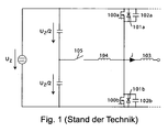
Eine Schaltung, die ein derartiges weiches Einschalten und Abschalten der Halbleiterschalter in einem Stromrichter ermöglicht, ist der so genannte Auxiliary-Resonant-Commutated-Pole-Inverter (ARCPI), der beispielsweise in der Veröffentlichung
Der ARCPI weist dabei den Nachteil auf, dass mit der Resonanzdrossel und dem Hilfsschalter zusätzliche Komponenten erforderlich sind, um Nullspannungsschalten zu ermöglichen. Diese Komponenten erhöhen den Bauteilaufwand und tragen nicht zur Leistungsübertragung bei. Ferner ist die Ansteuerung des Hilfsschalters 105 und der Halbleiterschalter 100a,b auf den durch die Resonanzdrossel 104 getriebenen Umschwingvorgang abzustimmen, wofür in der Regel aufwändige Treiberschaltungen vorgesehen werden müssen, die insbesondere Detektoren für den Zustand des Resonanzkreises umfassen.The ARCPI has the disadvantage that with the resonant choke and the auxiliary switch additional components are required to allow zero voltage switching. These components increase the component expenditure and do not contribute to the power transmission. Further, the control of the
Daher ist es eine Aufgabe der Erfindung, eine möglichst effiziente Umsetzung einer Eingangsspannung in eine Ausgangsspannung zu gewährleisten.It is therefore an object of the invention to ensure the most efficient conversion of an input voltage into an output voltage.
Die Aufgabe wird gelöst durch eine Schaltungsanordnung mit den Merkmalen des Patentanspruchs 1 und ein Verfahren zum Steuern dieser Schaltungsanordnung nach dem Patentanspruch 25. Ausgestaltungen der Schaltungsanordnung und des Verfahrens werden in den abhängigen Ansprüchen angegeben.The object is achieved by a circuit arrangement having the features of
Demgemäß ist nach einem ersten Aspekt der Erfindung vorgesehen, dass eine Schaltungsanordnung zum Umsetzen einer Eingangsspannung in eine Ausgangsspannung wenigstens eine Ausgangshalbbrücke und wenigstens eine Eingangshalbbrücke umfasst, die parallel zu einer Zwischenkreiskapazität zwischen eine obere und eine untere Spannungsschiene geschaltet sind. Jede Halbbrücke weist ein oberes Brückenelement, ein unteres Brückenelement und einen zugänglichen Mittelpunkt zwischen dem oberen und dem unteren Brückenelement auf, wobei die Brückenelemente eine Parallelschaltung eines Schaltelements und einer Kapazität umfassen. Dabei ist ein durch den Mittelpunkt einer Halbbrücke fließender Strom durch ein Schalten wenigstens eines Schaltelements der Brückenelemente der Halbbrücke von dem unteren Brückenelement auf das obere Brückenelement und umgekehrt kommutierbar. Der Mittelpunkt der Eingangshalbbrücke ist über eine Eingangsinduktivität mit einem Eingangsspannungsanschluss verbunden. Der Mittelpunkt der Ausgangshalbbrücke ist über eine Induktivität mit einem Ausgangsspannungsanschluss verbunden, und der Mittelpunkt der Eingangshalbbrücke ist über einen Koppelschalter mit dem Mittelpunkt der Ausgangshalbbrücke verbunden.Accordingly, it is provided according to a first aspect of the invention that a circuit arrangement for converting an input voltage into an output voltage comprises at least one output half-bridge and at least one input half-bridge, which are connected in parallel to a DC link capacitance between an upper and a lower voltage rail. Each half-bridge has an upper bridge element, a lower bridge element and an accessible mid-point between the upper and lower bridge elements, the bridge elements comprising a parallel connection of a switching element and a capacitor. In this case, a current flowing through the midpoint of a half-bridge can be commutated by switching at least one switching element of the bridge elements of the half-bridge from the lower bridge element to the upper bridge element and vice versa. The midpoint of the input half-bridge is connected to an input voltage terminal via an input inductance. The midpoint of the output half-bridge is connected via an inductor to an output voltage terminal, and the mid-point of the input half-bridge is connected via a coupling switch to the midpoint of the output half-bridge.
Die Erfindung beinhaltet die Idee, eine Schaltungsanordnung zur Umsetzung einer Eingangsspannung in eine Ausgangsspannung einzusetzen, die aus wenigstens einer Ausgangshalbbrücke und einer Eingangshalbbrücke aufgebaut ist, welche Brückenelemente zur Kommutierung der durch die Mittelpunkte der Halbbrücken fließenden Ströme aufweisen. Dabei kann die Eingangshalbbrücke beispielsweise im Hochsetzstellerbetrieb arbeiten und die Ausgangshalbbrücke im Tiefsetzstellerbetrieb Bei der Eingangsspannung und bei der Ausgangsspannung kann es sich jeweils um eine Gleichspannung oder eine ein- oder mehrphasige Wechselspannung handeln. Bei den Kapazitäten, die parallel zu den Schaltelementen der Brückenelemente geschaltet sind, kann es sich um die parasitären Kapazitäten der Schaltelemente handeln. Gleichfalls kann es jedoch auch vorgesehen sein, dass die Kapazitäten durch Kondensatoren gebildet werden, die zusätzlich parallel zu den Schaltelementen geschaltet sind.The invention includes the idea to use a circuit arrangement for converting an input voltage into an output voltage which is composed of at least one output half-bridge and one input half-bridge, which bridge elements for commutation of the currents flowing through the midpoints of the half-bridges. In this case, the input half-bridge can work, for example, in boost converter operation and the output half-bridge in buck converter operation. The input voltage and the output voltage can each be a DC voltage or a single- or multi-phase AC voltage. The capacitances connected in parallel with the switching elements of the bridge elements may be the parasitic capacitances of the switching elements. Likewise, however, it may also be provided that the capacitances are formed by capacitors, which are additionally connected in parallel with the switching elements.
Unter einer Kommutierung des Stroms von einem ersten Brückenelement auf ein zweites Brückenelement einer Halbbrücke wird ein Vorgang verstanden, bei dem ein Strompfad durch das erste Brückenelement abgeschaltet und ein Strompfad durch das zweite Brückenelement eingeschaltet wird. Ein derartiger Kommutierungsvorgang eines Stroms in einer Halbbrücke von einem ersten Brückenelement auf ein zweites Brückenelement kann bei der Schaltungsanordnung durch einen über den Koppelschalter zwischen den Mittelpunkten der Halbbrücken fließenden Strom derart unterstützt werden, dass ein Einschalten des zweiten Brückenelements durch Nullspannungsschalten erfolgen kann. Hierdurch werden die Schaltverluste der Schaltungsanordnung deutlich reduziert. Zudem ist der Koppelschalter dazu in der Lage, Energie von der Eingangshalbbrücke zur Ausgangshalbbrücke zu übertragen. Hierdurch können die Leitungsverluste der Schaltungsanordnung reduziert werden. Ein weiterer Vorteil der Schaltungsanordnung besteht darin, dass keine zusätzlichen passiven Bauelemente erforderlich sind, um einen weich schaltenden Betrieb zu realisieren. Hierdurch wird insbesondere die Ansteuerung der Schaltelemente der Brückenelemente vereinfacht, da der Zustand des Systems nicht von passiven Bauelemente abhängt. Insbesondere müssen keine Detektoren zur Erfassung des Zustands eines Schwingkreises vorgesehen werden.A commutation of the current from a first bridge element to a second bridge element of a half-bridge is understood to be a process in which a current path is switched off by the first bridge element and a current path is switched on by the second bridge element. Such a commutation of a current in a half-bridge from a first bridge element to a second bridge element can be supported in the circuit by a current flowing through the coupling switch between the midpoints of the half-bridges current such that switching on of the second bridge element can be done by zero voltage switching. As a result, the switching losses of the circuit arrangement are significantly reduced. In addition, the coupling switch is able to transfer energy from the input half-bridge to the output half-bridge. As a result, the line losses of the circuit can be reduced. Another advantage of the circuit arrangement is that no additional passive components are required to realize a soft-switching operation. As a result, in particular the control of the switching elements of the bridge elements is simplified, since the state of the system does not depend on passive components. In particular, no detectors for detecting the state of a resonant circuit need to be provided.
Das Verfahren sowie eine Ausgestaltung der Stromrichterschaltung sehen vor, dass bei einer Kommutierung des durch den Mittelpunkt einer Halbbrücke fließenden Stroms von einem ersten Brückenelement auf das zweite Brückenelement der Halbbrücke die Brückenelemente während einer Kommutierungsphase in einem Sperrzustand betrieben werden.The method and an embodiment of the converter circuit provide that, in the case of a commutation of the current flowing through the midpoint of a half-bridge, from a first bridge element to the second bridge element of the half-bridge, the bridge elements are operated in a blocking state during a commutation phase.
In dieser Ausgestaltung kann der Strom, der durch den Mittelpunkt der Halbbrücke fließt, dazu genutzt werden, die Kapazität des einzuschaltenden Brückenelements zu entladen, so dass ein Einschalten durch Nullspannungsschalten ermöglicht wird. Der Strom wird dabei zunächst dazu genutzt, die relevanten Kapazitäten umzuladen, bis schließlich eine Freilaufdiode bzw. eine als Schaltelement vorgesehene Diode des einzuschaltenden Brückenelements zu leiten beginnt. Das Entladen der Kapazität der einzuschaltenden Brückenelemente ist dabei mit dem Aufladen oder Entladen der Kapazitäten weiterer Brückenelemente verbunden, zu denen vom Mittelpunkt der betreffenden Halbbrücke eine leitende Verbindung besteht. Diese Umladevorgänge werden ebenfalls von dem Entladestrom der Kapazität des einzuschaltenden Brückenelements, bewirkt. Ein Strom, der geeignet ist, die Kapazität des einzuschaltenden Brückenelements zu entladen, bewirkt somit auch ein Auf- oder Entladen der weiteren Kapazitäten, zu denen eine leitende Verbindung besteht.In this embodiment, the current flowing through the mid-point of the half-bridge can be used to discharge the capacitance of the bridge element to be turned on, thereby enabling turn-on by zero-voltage switching. The current is first used to reload the relevant capacitances until finally a freewheeling diode or one as a switching element intended to initiate the diode of the bridge element to be turned on. The discharging of the capacitance of the bridge elements to be switched in is connected to the charging or discharging of the capacitances of further bridge elements to which there is a conductive connection from the midpoint of the relevant half bridge. These transhipment operations are also effected by the discharge current of the capacitance of the bridging element to be turned on. A current which is suitable for discharging the capacitance of the bridge element to be switched-on thus also causes a charging or discharging of the further capacitances to which there is a conductive connection.
Ferner sehen das Verfahren und eine Ausführungsform der Schaltungsanordnung vor, dass der Koppelschalter während einer Kommutierung eines durch den Mittelpunkt der Ausgangshalbbrücke in die Ausgangsinduktivität fließenden Ausgangsstroms von einem ersten Brückenelement auf ein zweites Brückenelement der Ausgangshalbbrücke eingeschaltet wird, wenn der Ausgangsstrom nach Betrag und/oder Vorzeichen nicht geeignet ist, ein Entladen der Kapazität des zweiten Brückenelements zu bewirken.Furthermore, the method and an embodiment of the circuit arrangement provide that the coupling switch is switched from a first bridge element to a second bridge element of the output half-bridge during commutation of an output current flowing through the center of the output half-bridge into the output inductance, if the output current is in magnitude and / or sign is not suitable to cause a discharge of the capacitance of the second bridge element.
Vorteilhaft kann in dieser Ausführungsform ein Kommutierungsvorgang in der Ausgangshalbbrücke durch einen über den Koppelschalter zwischen der Ausgangshalbbrücke und der Einganghalbbrücke fließenden Strom unterstützt werden, wenn der Ausgangsstrom der Ausgangshalbbrücke nicht geeignet ist, die Kapazität des einzuschaltenden Brückenelements zu entladen.Advantageously, in this embodiment, a commutation process in the output half-bridge can be assisted by a current flowing across the coupling switch between the output half-bridge and the input half-bridge when the output current of the output half-bridge is not suitable for discharging the capacitance of the bridge element to be turned on.
Es zeigt sich, dass bei eingeschaltetem Koppelschalter eine Differenz zwischen dem von der Eingangsinduktivität in den Mittelpunkt der Eingangshalbbrücke fließenden Strom und dem Ausgangsstrom der Ausgangshalbbrücke das Entladen der Kapazität bewirkt.It turns out that when the coupling switch is switched on, a difference between the current flowing from the input inductance to the center of the input half-bridge and the output current of the output half-bridge causes the capacity to be discharged.
Daher ist in einer verbundenen Ausgestaltung der Schaltungsanordnung und einer Ausführungsform des Verfahrens vorgesehen, dass ein während der Kommutierung durch die Eingangsinduktivität in den Mittelpunkt der Eingangshalbbrücke fließender Eingangsstrom derart eingestellt wird, dass eine Differenz zwischen diesem Eingangsstrom und dem Ausgangsstrom nach Betrag und Vorzeichen geeignet ist, ein Entladen der Kapazität des zweiten Brückenelements zu bewirken.It is therefore provided in a connected embodiment of the circuit arrangement and an embodiment of the method that during the commutation by the input inductance in the center of the input half-bridge flowing input current is set such that a difference between this input current and the output current in magnitude and sign is adapted to cause a discharge of the capacitance of the second bridge element.
In einer Ausgestaltung liegt die obere Spannungsschiene auf einem höheren Potenzial als die untere Spannungsschiene. Ferner wird der Eingangsstrom beispielsweise positiv gezählt, wenn er von der Eingangsinduktivität in den Mittelpunkt der Eingangshalbbrücke fließt. Der Ausgangsstrom wird beispielsweise positiv gezählt, wenn er von dem Mittelpunkt der Ausgangshalbbrücke in die Ausgangsinduktivität fließt.In one embodiment, the upper voltage rail is at a higher potential than the lower voltage rail. Further, the input current is positively counted, for example, as it flows from the input inductance to the center of the input half-bridge. For example, the output current is counted positive as it flows from the midpoint of the output half-bridge into the output inductance.
Unter diesen Voraussetzungen wird der Koppelschalter in einer Ausgestaltung der Schaltungsanordnung und des Verfahrens während einer Kommutierung eines durch den Mittelpunkt der Ausgangshalbbrücke in Richtung der Ausgangsinduktivität fließenden Ausgangsstrom von dem unteren zu dem oberen Brückenelement der Ausgangshalbbrücke eingeschaltet, falls der Ausgangsstrom nicht klein genug ist, um ein Entladen der Kapazität des oberen Brückenelements zu bewirken.Under these conditions, the coupling switch is turned on in an embodiment of the circuit arrangement and the method during commutation of an output current flowing through the center of the output half-bridge in the direction of Ausgangsinduktivität output current from the lower to the upper bridge element of the output half-bridge, if the output current is not small enough to Unload the capacity of the upper bridge element to effect.
Bei einer verbundenen Ausführungsform ist vorgesehen, dass der während der Kommutierung durch die Induktivität der Eingangshalbbrücke in den Mittelpunkt der Eingangshalbbrücke fließende Eingangsstrom derart eingestellt wird, dass er so groß ist, dass eine Differenz zwischen diesem Eingangsstrom und dem Ausgangsstrom ausreichend groß ist, um ein Entladen der Kapazität des oberen Brückenelements zu bewirken.In a connected embodiment it is provided that the input current flowing during the commutation through the inductance of the input half-bridge into the center of the input half-bridge is set to be so large that a difference between this input current and the output current is sufficiently large to cause a discharge To effect the capacity of the upper bridge element.
Darüber hinaus beinhaltet eine Ausführungsform unter den zuvor genannten Voraussetzungen, dass der Koppelschalter während einer Kommutierung des durch den Mittelpunkt der Ausgangshalbbrücke in Richtung der Induktivität der Ausgangshalbbrücke fließenden Ausgangsstroms von dem oberen auf das unteren Brückenelement der Ausgangshalbbrücke eingeschaltet wird, falls der Ausgangsstrom nicht groß genug ist, um ein Entladen der Kapazität des unteren Brückenelements der Ausgangshalbbrücke zu bewirken.In addition, an embodiment under the aforementioned conditions includes that the coupling switch is turned on during commutation of the current flowing through the center of the output half-bridge in the direction of the inductance of the output half-bridge output current from the upper to the lower bridge element of the output half-bridge, if Output current is not large enough to cause a discharge of the capacity of the lower bridge element of the output half-bridge.
Hiermit verbunden ist eine Ausgestaltung, bei der vorgesehen ist, dass der während der Kommutierung durch die Induktivität der Eingangshalbbrücke in den Mittelpunkt der Eingangshalbbrücke fließende Eingangsstrom so eingestellt wird, dass eine Differenz zwischen diesem Eingangsstrom und dem Ausgangsstrom geeignet ist, ein Entladen der Kapazität des unteren Brückenelements der Ausgangshalbbrücke zu bewirken.Associated with this is an embodiment in which it is provided that the input current flowing during the commutation through the inductance of the input half-bridge into the center of the input half-bridge is adjusted so that a difference between this input current and the output current is suitable, a discharge of the capacity of the lower one Bridging element of the output half-bridge to effect.
Bei einer Weiterbildung der Schaltungsanordnung und des Verfahrens ist vorgesehen, dass der Koppelschalter ausgeschaltet wird, wenn sich sowohl das obere Brückenelement der Eingangshalbbrücke als auch das untere Brückenelement der Ausgangshalbbrücke in einem leitenden Zustand befinden, oder wenn sich sowohl das untere Brückenelement der Eingangshalbbrücke als auch das obere Brückenelement der Ausgangshalbbrücke in einem leitenden Zustand befinden.In a further development of the circuit arrangement and the method is provided that the coupling switch is turned off when both the upper bridge element of the input half-bridge and the lower bridge element of the output half-bridge are in a conductive state, or if both the lower bridge element of the input half-bridge and the upper bridge element of the output half-bridge are in a conductive state.
Vorteilhaft wird hierdurch insbesondere verhindert, dass die Zwischenkreiskapazität eingeschaltetem Koppelschalter kurzgeschlossen wird.Advantageously, this prevents in particular that the DC link capacity switched coupling switch is short-circuited.
Darüber hinaus beinhaltet eine Weiterbildung der Schaltungsanordnung und des Verfahrens, dass der Koppelschalter nur dann eingeschaltet wird, wenn sich die oberen Brückenelemente der Eingangshalbbrücke und der Ausgangshalbbrücke jeweils in einem leitenden Zustand oder in einem Sperrzustand befinden.In addition, a development of the circuit arrangement and the method that the coupling switch is only turned on when the upper bridge elements of the input half-bridge and the output half-bridge are each in a conductive state or in a blocking state.
Es hat sich gezeigt, dass hierdurch eine besonders einfache Ansteuerung des Koppelschalters erreicht werden kann, bei der sowohl einer weich schaltender Betrieb der Schaltungsanordnung möglich ist, als auch eine Energieübertragung von der Eingangshalbbrücke zu der Ausgangshalbbrücke über den Koppelschalter erfolgen kann.It has been shown that in this way a particularly simple control of the coupling switch can be achieved, in which both a soft-switching operation of the circuit arrangement is possible, as well as an energy transfer from the input half bridge to the output half bridge can be done via the coupling switch.
Der Eingangsstrom der Eingangshalbbrücke und der Ausgangsstrom der Ausgangshalbbrücke variieren zwischen Minimal- und Maximalwerten. Die Extremwerte werden dabei, jeweils bei einer Kommutierung des Stroms von einem ersten Brückenelement der betreffenden Halbbrücke auf ein zweites Brückenelement der Halbbrücke angenommen.The input current of the input half-bridge and the output current of the output half-bridge vary between minimum and maximum values. The extreme values are assumed, in each case with a commutation of the current from a first bridge element of the relevant half-bridge to a second bridge element of the half-bridge.
Daher sieht eine Ausgestaltung der Schaltungsanordnung und des Verfahrens vor, dass eine Kommutierung des von dem Mittelpunkt der Ausgangshalbbrücke in die Ausgangsinduktivität fließenden Ausgangsstroms von einem ersten Brückenelement auf ein zweites Brückenelement der Ausgangshalbbrücke, bei welcher der Koppelschalter eingeschaltet wird, mit der Kommutierung des von der Eingangsinduktivität in den Mittelpunkt der Eingangshalbbrücke fließenden Eingangsstroms von einem ersten Brückenelement auf ein zweites Brückenelement der Eingangshalbbrücke synchronisiert wird, bei welcher der Eingangsstrom derart eingestellt ist, dass die Differenz zwischen dem Eingangsstrom und den Ausgangsstrom nach Betrag und Vorzeichen geeignet ist, ein Entladen der Kapazität des zweiten Brückenelements der Ausgangshalbbrücke zu bewirken.Therefore, an embodiment of the circuit arrangement and the method provides that a commutation of the output current flowing from the center of the output half-bridge into the output inductance from a first bridge element to a second bridge element of the output half-bridge, in which the coupling switch is turned on, with the commutation of the input of the input inductance synchronized in the center of the input half-bridge input current flowing from a first bridge element to a second bridge element of the input half-bridge, wherein the input current is set so that the difference between the input current and the output current in magnitude and sign is suitable, discharging the capacity of the second Bridging element of the output half-bridge to effect.
Es hat sich gezeigt, dass bei einer derartigen Synchronisierung besonders einfach sichergestellt werden kann, dass der in die Eingangshalbbrücke fließende Strom geeignet ist, die Kommutierung des Ausgangsstroms von dem unteren Brückenelement auf das obere Brückenelement der Ausgangshalbbrücke derart zu unterstützen, dass ein Einschalten des oberen Brückenelements durch Nullspannungsschalten erfolgen kann.It has been found that with such a synchronization it can be ensured in a particularly simple manner that the current flowing into the input half-bridge is suitable for assisting the commutation of the output current from the lower bridge element to the upper bridge element of the output half-bridge such that switching on of the upper bridge element can be done by zero voltage switching.
Eine Ausgestaltung der Schaltungsanordnung und des Verfahrens zeichnet sich dadurch aus, dass ein aus der Eingangsinduktivität in die Eingangshalbbrücke fließender Strom so eingestellt wird, dass er während der Kommutierung von einem ersten Brückenelement auf ein zweites Brückenelement der Eingangshalbbrücke nach Betrag und/oder Vorzeichen geeignet ist, während der Kommutierungsphase ein Entladen der Kapazität des zweiten Brückenelements zu bewirken.An embodiment of the circuit arrangement and of the method is characterized in that a current flowing from the input inductance into the input half-bridge is adjusted so that it is suitable for magnitude and / or sign during the commutation from a first bridge element to a second bridge element of the input half-bridge. during the commutation phase to cause a discharge of the capacitance of the second bridge element.
Hierdurch wird sichergestellt, dass sich die Kapazität des einzuschaltenden Brückenelements der Eingangshalbbrücke geschaltet ist, während des Kommutierungsvorgangs entladen wird, so dass der einzuschaltende Schalter durch ein Nullspannungsschalten eingeschaltet werden kann. Der Betrieb der Eingangshalbbrücke entspricht in dieser Ausführungsform dem so genannten Resonant-Pole-Verfahren.This ensures that the capacitance of the bridging element of the input half-bridge to be turned on is switched off during the commutation process, so that the switch to be switched on can be switched on by zero-voltage switching. The operation of the input half-bridge corresponds in this embodiment to the so-called resonant-pole method.
Eine Ausführungsform der Schaltungsanordnung und des Verfahrens ist dadurch gekennzeichnet, dass die Ausgangshalbbrücke mit einer Frequenz getaktet wird, die gleich der Frequenz der Eingangshalbbrücke ist, und/oder dass die Frequenz der Eingangshalbbrücke ein ganzzahliges Vielfaches der Frequenz der Ausgangshalbbrücke ist.An embodiment of the circuit arrangement and the method is characterized in that the output half-bridge is clocked at a frequency which is equal to the frequency of the input half-bridge, and / or that the frequency of the input half-bridge is an integer multiple of the frequency of the output half-bridge.
Vorteilhaft wird hierdurch eine Synchronisierung ermöglicht, die es erlaubt, den Koppelschalter in einfacher Weise anzusteuern.Advantageously, thereby a synchronization is made possible, which allows to control the coupling switch in a simple manner.
In einer weiteren Ausgestaltung der Schaltungsanordnung und des Verfahrens ist vorgesehen, dass mehrere elektrisch parallel zu der Zwischenkreiskapazität geschaltete Ausgangshalbbrücken vorgesehen sind, die als ein ein- oder mehrphasiger Wechselrichter betrieben werden.In a further embodiment of the circuit arrangement and of the method, it is provided that a plurality of output half-bridges, which are connected electrically in parallel with the intermediate circuit capacitance, are provided, which are operated as a single- or multi-phase inverter.
In dieser Ausgestaltung kann die Schaltungsanordnung vorteilhaft als ein ein- oder mehrphasiger Wechselrichter betrieben werden, der eine Eingangsspannung in eine ein- oder mehrphasige Wechselspannung umsetzt.In this embodiment, the circuit arrangement can be advantageously operated as a single- or multi-phase inverter, which converts an input voltage into a single-phase or multi-phase AC voltage.
Insbesondere kann die Schaltungsanordnung als ein dreiphasiger Wechselrichter betrieben werden. In dieser Ausgestaltung sind vorzugsweise drei Ausgangshalbbrücke vorgesehen, die elektrisch parallel zu der Zwischenkreiskapazität geschaltet sind. In dieser Ausgestaltung kann die Schaltungsanordnung ausgangsseitig beispielsweise an ein Drehstromnetz angeschlossen werden.In particular, the circuit arrangement can be operated as a three-phase inverter. In this embodiment, preferably three output half-bridge are provided which are electrically parallel to the DC link capacitance are switched. In this embodiment, the circuit arrangement can be connected on the output side, for example, to a three-phase network.
Bei einem Betrieb als einphasiger Wechselrichter sind vorzugsweise zwei elektrisch parallel zu der Zwischenkreiskapazität geschaltete Ausgangshalbbrücken vorgesehen.In the case of operation as a single-phase inverter, two output half-bridges connected electrically in parallel with the intermediate circuit capacitance are preferably provided.
Eine Weiterbildung der Schaltungsanordnung und des Verfahrens zeichnet sich dadurch aus, dass ein bidirektionaler Betrieb vorgesehen ist, wobei die Ausgangshalbbrücken in einem Betriebsmodus als Gleichrichter betrieben werden können.A development of the circuit arrangement and the method is characterized in that a bidirectional operation is provided, wherein the output half-bridges can be operated in an operating mode as a rectifier.
Vorzugsweise handelt es sich hierbei um einen Betriebsmodus, bei dem Energie von den Ausgangsspannungsanschlüssen zu dem Eingangsspannungsschluss bzw. den Eingangsspannungsanschlüssen übertragen wird. In einem weiteren Betriebsmodus, in dem Energie von dem Eingangsspannungsanschluss oder den Eingangsspannungsanschlüssen zu Ausgangsspannungsanschlüssen transportiert wird, arbeiten die Ausgangshalbbrücken wie zuvor beschrieben vorzugsweise im Wechselrichterbetrieb. Der oder die Koppelschalter werden im bidirektionalen Betrieb vorzugsweise bidirektional ausgeführt,d.h., dass sie Sperrspannung in beide Richtungen aufnehmen können und Strom in beide Richtungen leiten können.Preferably, this is an operating mode in which power is transferred from the output voltage terminals to the input voltage terminal (s). In a further mode of operation in which energy is transported from the input voltage terminal or input voltage terminals to output voltage terminals, the output half-bridges operate preferably in inverter mode as previously described. The one or more coupling switches are preferably carried out bidirectionally in bidirectional operation, that is, that they can absorb reverse voltage in both directions and can conduct electricity in both directions.
Eine Ausgestaltung der Schaltungsanordnung und des Verfahrens zeichnet sich dadurch aus, dass drei elektrisch parallel zu der Zwischenkreiskapazität geschaltete Eingangshalbbrücken vorgesehen sind, wobei die Mittelpunkte der Ausgangshalbbrücken jeweils über einen Koppelschalter mit genau einem Mittelpunkt einer Eingangshalbbrücke verbunden sind.An embodiment of the circuit arrangement and the method is characterized in that three are provided electrically parallel to the intermediate circuit capacitance switched input half-bridges, the centers of the output half-bridges are each connected via a coupling switch with exactly one center of an input half-bridge.
Vorteilhaft ist bei dieser Ausgestaltung jeder Ausgangshalbbrücke der Wechselrichterschaltung eine Eingangshalbbrücke zugeordnet, die ein Nullspannungsschalten in der betreffenden Ausgangshalbbrücke unterstützt.Advantageously, in this embodiment, each output half-bridge of the inverter circuit is associated with an input half-bridge, which supports zero-voltage switching in the respective output half-bridge.
Eine Ausgestaltung der Schaltungsanordnung und des Verfahrens ist dadurch gekennzeichnet, dass die Mittelpunkte der Eingangshalbbrücken über jeweils eine Eingangsinduktivität mit einem Eingangsspannungsanschluss verbunden sind.An embodiment of the circuit arrangement and the method is characterized in that the centers of the input half-bridges are each connected via an input inductance with an input voltage terminal.
Eine alternative Ausgestaltung der Schaltungsanordnung und des Verfahrens sieht vor, dass die elektrisch parallel zu der Zwischenkreiskapazität geschalteten Ausgangshalbbrücken über jeweils einen Koppelschalter mit genau einer Eingangshalbbrücke verbunden sind.An alternative embodiment of the circuit arrangement and the method provides that the output half-bridges, which are electrically connected in parallel to the intermediate circuit capacitance, are connected via exactly one coupling switch to exactly one input half-bridge.
In dieser Ausgestaltung ist lediglich eine Eingangshalbbrücke vorgesehen, mit der die Ausgangshalbbrücken des Wechselrichters verbunden sind. Hierdurch können sich zwar Einschränkungen in Bezug auf den weich schaltenden Betrieb der Ausgangshalbbrücken ergeben, die Ansteuerung des Wechselrichters wird jedoch bei Verwendung einer einzigen Eingangshalbbrücke deutlich vereinfacht und der Materialaufwand reduziert.In this embodiment, only one input half-bridge is provided, with which the output half-bridges of the inverter are connected. Although this may result in restrictions with respect to the soft switching operation of the output half bridges, the control of the inverter is significantly simplified when using a single input half bridge and reduces the cost of materials.
Eine Weiterbildung der Schaltungsanordnung und des Verfahrens ist dadurch gekennzeichnet, dass die den Wechselrichter bildenden Ausgangshalbbrücken nach Maßgabe einer 120°-Flattop-Modulation angesteuert werden, so dass die Brückenelemente jeweils einer Ausgangshalbbrücke für ein Drittel der Periode des mittleren Ausgangsstroms der Ausgangshalbbrücke nicht geschaltet werden.A development of the circuit arrangement and of the method is characterized in that the inverters forming output half-bridges are controlled in accordance with a 120 ° flattop modulation, so that the bridge elements are not connected in each case an output half-bridge for one third of the period of the average output current of the output half-bridge.
Dabei hat sich gezeigt, dass sich bei Ansteuerung des Wechselrichters anhand des 120°-Flattop-Verfahrens auch bei Verwendung nur einer Eingangshalbbrücke ein nahezu dauerhafter weich schaltender Betrieb der Ausgangshalbbrücken realisieren lässt.It has been shown that when the inverter is controlled by means of the 120 ° flat-top method, even when only one input half-bridge is used, a virtually permanent soft-switching operation of the output half-bridges can be realized.
Bei einer weiteren Ausführungsform der Schaltungsanordnung ist vorgesehen, dass zwei elektrisch parallel zu der Zwischenkreiskapazität geschaltete Eingangshalbbrücken vorgesehen sind, deren Mittelpunkte jeweils über eine Eingangsinduktivität an einen Pol der Eingangsspannung angeschlossen sind, wobei eine erste Eingangshalbbrücke im Hochsetzstellerbetrieb und eine zweite Halbbrücke im Tiefsetzstellerbetrieb arbeitet, und wobei der Mittelpunkt der Ausgangshalbbrücke über jeweils einen Koppelschalter mit den Mittelpunkten der Eingangshalbbrücken verbunden sind.In a further embodiment of the circuit arrangement, it is provided that two input half bridges, which are electrically connected in parallel to the intermediate circuit capacitance, are provided are provided, whose centers are each connected via an input inductance to a pole of the input voltage, wherein a first input half-bridge in Hochsetzstellerbetrieb and a second half-bridge operates in buck converter mode, and wherein the center of the output half-bridge are connected via a coupling switch with the centers of the input half-bridges.
Bei einer verbundenen Ausgestaltung der Schaltungsanordnung und des Verfahrens ist vorgesehen, dass einer der Koppelschalter während einer Kommutierung eines durch den Mittelpunkt der Ausgangshalbbrücke in Richtung der Ausgangsinduktivität fließenden Ausgangsstroms von einem ersten Brückenelement auf ein zweites Brückenelement der Ausgangshalbbrücke eingeschaltet wird, falls der Ausgangsstrom nach Betrag und/oder Richtung nicht geeignet ist, ein Entladen der Kapazität des zweiten Brückenelements zu bewirken.In a connected embodiment of the circuit arrangement and the method, it is provided that one of the coupling switches is switched on during a commutation of a current flowing through the center of the output half-bridge in the direction of Ausgangsinduktivität output current from a first bridge element to a second bridge element of the output half-bridge, if the output current in magnitude and / Direction is not suitable to cause a discharge of the capacity of the second bridge element.
Darüber hinaus ist es bei einer verbundenen Ausgestaltung der Schaltungsanordnung und des Verfahrens vorgesehen, dass derjenige Koppelschalter eingeschaltet wird, der den Mittelpunkt der Ausgangshalbbrücke mit dem Mittelpunkt der Eingangshalbbrücke verbindet, die so ausgewählt ist, dass der während der Kommutierung durch die Induktivität der Eingangshalbbrücke in den Mittelpunkt der Eingangshalbbrücke fließende Eingangsstrom so eingestellt ist, dass eine Differenz zwischen diesem Eingangsstrom und dem Ausgangsstrom geeignet ist, ein Entladen der Kapazität des zweiten Brückenelements der Ausgangshalbbrücke zu bewirken.Moreover, it is provided in a connected embodiment of the circuit arrangement and the method that the coupling switch is turned on, which connects the center of the output half-bridge with the center of the input half-bridge, which is selected so that during commutation by the inductance of the input half-bridge in the Center of the input half-bridge flowing input current is set so that a difference between this input current and the output current is adapted to cause a discharge of the capacitance of the second bridge element of the output half-bridge.
Bei einer Weiterbildung der Schaltungsanordnung und des Verfahrens ist vorgesehen, dass die Eingangshalbbrücken als einphasiger oder mehrphasiger Gleichrichter betrieben werden.In a development of the circuit arrangement and the method, it is provided that the input half-bridges are operated as a single-phase or multi-phase rectifier.
Vorteilhaft kann die Schaltungsanordnung somit als ein Umrichter betrieben werden, der eine Wechselspannung bzw. eine mehrphasige Eingangsspannung in eine Ausgangsspannung umsetzen kann. Im Falle eines einphasigen Gleichrichters sind dabei wenigstens zwei Eingangshalbbrücken vorgesehen, im Falle eines dreiphasigen Gleichrichters vorzugsweise drei Eingangshalbbrücken.Advantageously, the circuit arrangement can thus be operated as a converter, which can convert an AC voltage or a multi-phase input voltage into an output voltage. In the case of a single-phase rectifier are at least two input half-bridges provided, in the case of a three-phase rectifier preferably three input half-bridges.
Ferner sieht eine Ausgestaltung der Schaltungsanordnung und des Verfahrens vor, dass es sich bei dem Schaltelement des unteren Brückenelements der Eingangshalbbrücke und bei dem Schaltelement des oberen Brückenelements der Ausgangshalbbrücke jeweils um einen Transistor mit antiparallel geschalteter Freilaufdiode handelt.Furthermore, an embodiment of the circuit arrangement and of the method provides that the switching element of the lower bridge element of the input half-bridge and the switching element of the upper bridge element of the output half-bridge are each a transistor with antiparallel-connected freewheeling diode.
Eine Weiterbildung der Schaltungsanordnung und des Verfahrens beinhaltet, dass es sich bei dem Schaltelement des oberen Brückenelements der Eingangshalbbrücke und bei dem Schaltelement des oberen Brückenelements der Ausgangshalbbrücke jeweils um einen Transistor mit antiparallel geschalteter Freilaufdiode oder um eine Diode handelt, die derart geschaltet ist, dass sie sich in einem Sperrzustand befindet, wenn das Schaltelement des gegenüberliegenden Brückenelements leitend geschaltet ist.A refinement of the circuit arrangement and of the method includes that the switching element of the upper bridge element of the input half-bridge and the switching element of the upper bridge element of the output half-bridge are each a transistor with antiparallel-connected freewheeling diode or a diode which is connected in such a way that it is in a blocking state when the switching element of the opposite bridge element is turned on.
Eine Ausführungsform der Schaltungsanordnung und des Verfahrens beinhaltet, dass der Koppelschalter wenigstens einen Transistor umfasst, dessen Source- oder Emitteranschluss mit dem Mittelpunkt der Eingangshalbbrücke oder der Ausgangshalbbrücke verbunden ist, wobei eine Treiberschaltung des Transistors anhand eines Bootstrap-Verfahrens gespeist wird.An embodiment of the circuit arrangement and the method includes that the coupling switch comprises at least one transistor whose source or emitter terminal is connected to the midpoint of the input half-bridge or the output half-bridge, wherein a drive circuit of the transistor is fed by a bootstrap method.
Dies erlaubt es, die Treiberschaltung für den Koppelschalter besonders einfach auszuführen.This makes it particularly easy to perform the driver circuit for the coupling switch.
Bei einer weiteren Ausgestaltung der Schaltungsanordnung und des Verfahrens ist vorgesehen, dass die Brückenelemente und die Koppelschalter in einem Modul untergebracht sind.In a further embodiment of the circuit arrangement and the method is provided that the bridge elements and the coupling switches are housed in a module.
Vorteilhaft können hierdurch insbesondere Streuinduktivitäten deutlich reduziert werden. Die Brückenelemente und die Koppelschalter können innerhalb des Moduls beispielsweise durch Bonden miteinander verbunden werden.In this way, in particular, leakage inductances can be significantly reduced. The bridge elements and the coupling switches can be connected to each other within the module, for example by bonding.
Darüber hinaus sieht eine Ausführungsform der Schaltungsanordnung und des Verfahrens vor, dass eine Treiberschaltung wenigstens teilweise in das Modul integriert ist.In addition, an embodiment of the circuit arrangement and the method provide that a driver circuit is at least partially integrated into the module.
Die erfindungsgemäße Schaltungsanordnung erlaubt aufgrund der weich schaltenden Betriebsmodi eine sehr effiziente Energieübertragung. Ferner kann die Eingangsspannung in einem sehr weiten Bereich variiert werden. Daher eignet sie sich besonders gut für die Einspeisung einer in einem Photovoltaikgenerator, einer Brennstoffzelle oder einer Windkraftanlage erzeugten Energie in ein Stromnetz. Gleichfalls kann die Schaltung auch durch einen anderem Generator oder eine Batterie gespeist werden. Vorteilhaft kann mit der Schaltungsanordnung insbesondere ein Motor, beispielsweise ein Synchron- oder Asynchronmotor, mit Energie versorgt werden.The circuit arrangement according to the invention allows a very efficient energy transfer due to the soft-switching operating modes. Furthermore, the input voltage can be varied within a very wide range. Therefore, it is particularly suitable for feeding a generated in a photovoltaic generator, a fuel cell or a wind turbine power into a power grid. Likewise, the circuit can also be powered by another generator or a battery. Advantageously, with the circuit arrangement, in particular a motor, for example a synchronous or asynchronous motor, be supplied with energy.
In Ausgestaltungen der Schaltungsanordnung wird der Eingangsspannungsanschluss der Schaltungsanordnung daher durch einen Photovoltaikgenerator, eine Windkraftfanlage oder eine Brennstoffzelle versorgt. Die Ausgangsspannungsanschlüsse können beispielsweise an ein Drehstromsystem angeschlossen sein.In embodiments of the circuit arrangement, the input voltage terminal of the circuit arrangement is therefore supplied by a photovoltaic generator, a Windkraftfanlage or a fuel cell. The output voltage terminals may be connected, for example, to a three-phase system.
Die zuvor genannten sowie weitere Vorteile, Besonderheiten und zweckmäßige Weiterbildungen der Erfindung werden auch anhand der Ausführungsbeispiele deutlich, die im Folgenden unter Bezugnahme auf die Figuren beschrieben werden.The above-mentioned and other advantages, features and expedient developments of the invention will become apparent from the embodiments, which are described below with reference to the figures.
Von den Figuren zeigt
- Fig. 1
- einen Brückenzweig eines Auxiliary-Resonant-Commutad-Pole-Inverter nach dem Stand der Technik,
- Fig. 2
- ein Schaltdiagramm eines Gleichstromstellers in einer ersten Ausführungsform,
- Fig. 3
- schematische Diagramme, mit den zeitlichen Verläufen der Leitfähigkeitszustände der Halbleiterschalter und verschiedener Ströme innerhalb des in
Figur 2 - Fig. 4
- ein Schaltdiagramm eines Gleichstromstellers in einer zweiten Ausführungsform,
- Fig. 5
- ein Schaltdiagramm eines Gleichstromstellers in einer dritten Ausführungsform,
- Fig. 6
- ein Schaltdiagramm eines dreiphasigen Wechselrichters in einer ersten Ausführungsform,
- Fig. 7
- ein Diagramm mit einer Veranschaulichung der zeitlichen Verläufe der Mittelwerte, Maximalwerte und Minimalwerte eines Eingangsstroms sowie eines Ausgangsstroms des in der
Figur 6 dargestellten Wechselrichters in einer ersten Betriebsart des Wechselrichters, - Fig. 8
- ein Diagramm mit einer Veranschaulichung der zeitlichen Verläufe der Mittelwerte, Maximalwerte und Minimalwerte eines Eingangsstroms sowie eines Ausgangsstroms des in der
Figur 6 dargestellten Wechselrichters in einer zweiten Betriebsart des Wechselrichters, - Fig. 9
- ein Diagramm mit einer Veranschaulichung der zeitlichen Verläufe der Mittelwerte, Maximalwerte und Minimalwerte eines Eingangsstroms sowie eines Ausgangsstroms des in der
Figur 6 dargestellten Wechselrichters in einer zweiten Betriebsart des Wechselrichters, - Fig. 10
- ein Schaltdiagramm eines dreiphasigen Wechselrichters in einer zweiten Ausführungsform,
- Fig. 11
- ein Schaltdiagramm eines dreiphasigen Wechselrichters in einer dritten Ausführungsform,
- Fig. 12
- ein Schaltdiagramm eines dreiphasigen Wechselrichters in einer vierten Ausführungsform,
- Fig. 13
- ein Schaltdiagramm eines Umrichters zum Umsetzen einer dreiphasigen Eingangsspannung in eine dreiphasige Ausgangsspannung und
- Fig. 14
- ein Schaltdiagramm eines einphasigen Wechselrichters.
- Fig. 1
- a bridge branch of a prior art Auxiliary Resonant Commutad Pole Inverter,
- Fig. 2
- FIG. 3 is a circuit diagram of a DC chopper in a first embodiment; FIG.
- Fig. 3
- schematic diagrams, with the time courses of the conductivity states of the semiconductor switches and various currents within the in
FIG. 2 illustrated DC actuator, - Fig. 4
- FIG. 2 is a circuit diagram of a DC regulator in a second embodiment; FIG.
- Fig. 5
- FIG. 2 is a circuit diagram of a DC chopper in a third embodiment; FIG.
- Fig. 6
- FIG. 3 is a circuit diagram of a three-phase inverter in a first embodiment; FIG.
- Fig. 7
- a diagram with an illustration of the time courses of the average values, maximum values and minimum values of an input current and an output current of the in the
FIG. 6 shown inverter in a first mode of operation of the inverter, - Fig. 8
- a diagram with an illustration of the time courses of the average values, maximum values and minimum values of an input current and an output current of the in the
FIG. 6 shown inverter in a second mode of operation of the inverter, - Fig. 9
- a diagram with an illustration of the time courses of the average values, maximum values and minimum values of an input current and an output current of the in the
FIG. 6 shown inverter in a second mode of operation of the inverter, - Fig. 10
- a circuit diagram of a three-phase inverter in a second embodiment,
- Fig. 11
- a circuit diagram of a three-phase inverter in a third embodiment,
- Fig. 12
- FIG. 3 is a circuit diagram of a three-phase inverter in a fourth embodiment; FIG.
- Fig. 13
- a circuit diagram of an inverter for converting a three-phase input voltage into a three-phase output voltage and
- Fig. 14
- a circuit diagram of a single-phase inverter.
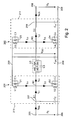
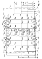
Die Eingangsstufe 213 enthält eine Eingangshalbbrücke 201. Diese umfasst eine Reihenschaltung zweier Halbleiterschalter S1 und S2, die zwischen die obere Spannungsschiene 203 und die untere Spannungsschiene 204 parallel zu der Zwischenkreiskapazität CDC geschaltet sind. Parallel zu den Halbleiterschaltern S1 und S2 sind Kapazitäten C1 und C2 geschaltet. Der zugängliche Mittelpunkt M1 der Eingangshalbbrücke 201 zwischen den Halbleiterschaltern S1 und S2 ist eingangsseitig über eine durch eine Spule gebildete Induktivität L1 mit einem ersten Pol 205 einer Eingangsgleichspannung UE verbunden. Die untere Spannungsschiene 204 ist bei der dargestellten Schaltungsanordnung mit dem zweiten Pol 206 der Eingangsspannung UE verbunden und liegt auf einem geringeren Potenzial als die oberen Spannungsschiene 203. Zur Stützung der Eingangsspannung UE ist eine Kapazität CE vorgesehen, die parallel zur Eingangsspannung UE geschaltet ist. Der Eingangsstrom iEIN des Gleichstromstellers verzweigt sich an dem Punkt 207 in einen Strom, der in die Kapazität CE fließt und in den Eingangsstrom iL1, der über die Induktivität L1 in den Mittelpunkt M1 der Eingangshalbbrücke 201 fließt.The
Die Ausgangsstufe 211 enthält eine Ausgangshalbbrücke 202. die in ähnlicher Weise wie die Eingangshalbbrücke 201 ist die Ausgangshalbbrücke 202 aufgebaut ist. Sie umfasst gleichfalls eine Reihenschaltung zweier Halbleiterschalter S3 und S4 mit parallel zu den Halbleiterschaltern S3 und S4 geschalteten Kapazitäten C3 und C4 und antiparallel geschalteten Dioden D3 und D4. Die Reihenschaltung ist parallel zu der Zwischenkreiskapazität CDC zwischen die obere Spannungsschiene 203 und die untere Spannungsschiene 204 geschaltet und verfügt über einen zugänglichen Mittelpunkt M2 zwischen den beiden Halbleiterschaltern S3 und S4, der über eine Induktivität L2 mit einem ersten Pol 208 der Ausgangsspannung UA verbunden ist. Der zweite Pol 209 der Ausgangsspannung UA ist mit der unteren Spannungsschiene 204 verbunden. Zur Glättung der Ausgangsspannung UA ist eine parallel zu der Ausgangsspannung UA geschaltete Kapazität CA vorgesehen. Der von dem Mittelpunkt M2 der Ausgangshalbbrücke 202 über die Induktivität L2 fließende Strom Ausgangsstrom iL2 der Ausgangshalbbrücke 202 verzweigt sich an dem Punkt 210 in einen Strom, der in die Glättungskapazität CA fließt und den Ausgangsstrom iAUS des Gleichstromstellers.The
Der Mittelpunkt M1 der Eingangshalbbrücke 201 und der Mittelpunkt M2 der Ausgangsstufe 202 sind über einen Koppelschalter S5 miteinander verbunden, zu dem eine Kapazität C5 elektrisch parallel geschaltet ist. In der dargestellten Ausgestaltung handelt es sich bei dem Koppelschalter S5 um einen bidirektionalen Schalter, der in beide Richtungen Sperrspannung aufnehmen und Strom leiten kann. Bei Verwendung eines bidirektionalen Koppelschalters ist eine bidirektionale Leistungsübertragung im weichschaltenden Betrieb aller Schalter S1-S5 möglich, bei dem über die Eingangshalbbrücke 201 eingespeiste Leistung zur Ausgangsstufe 202 sowie über die Ausgangsstufe eingespeiste Leistung zur Eingangshalbbrücke 201 übertragen werden kann. Anstelle eines bidirektionalen Koppelschalters S5 kann auch ein unidirektionaler Koppelschalter S5' eingesetzt werden, der in beide Richtung Sperrspannung aufnehmen, Strom jedoch nur in eine Richtung leiten kann. Der unidirektionale Koppelschalter S5' ermöglicht je nach Polung einen Stromfluss vom Mittelpunkt M1 der Eingangshalbbrücke 201 zum Mittelpunkt M2 der Ausgangsstufe 202 oder umgekehrt. Wie weiter unten noch erläutert wird, wird die Leitungsrichtung eines unidirektionalen Koppelschalters S5' entsprechend dem Arbeitspunkt des Gleichstromstellers so gewählt, dass ein weich schaltender Betrieb der Ausgangshalbbrücke ermöglicht wird.The center M1 of the
Die in der Eingangshalbbrücke 201 und der Ausgangshalbbrücke 202 verwendeten Halbleiterschalter S1-S4 sind beispielsweise als Leistungs-MOSFETs (MOSFET: Metal Oxide Semiconductor Field Effect Transistor) ausgeführt, welche über die in der
Die Ansteuerung der Halbleiterschalter S1 und S2 der Eingangshalbbrücke 201 und der Halbleiterschalter S3 und S4 der Ausgangsbrücke 202 sowie der Koppelschalter geschieht durch eine Treiberschaltung, die in der
Die Schaltungsanordnung ist vorzugsweise vollständig in ein Modul integriert, so dass Streuinduktivitäten gering gehalten werden. Die Bauelemente können dabei beispielsweise durch Bonden miteinander verbunden werden. Darüber hinaus kann auch die Treiberschaltung wenigstens teilweise in das Modul integriert werden.The circuit arrangement is preferably completely integrated in a module, so that stray inductances are kept low. The components can be connected to each other, for example by bonding. In addition, the driver circuit can be at least partially integrated into the module.
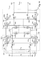
Die Eingangshalbbrücke 201 arbeitet bei einem Leistungstransport von der Eingangshalbbrücke 201 zu der Ausgangshalbbrücke 202, d.h. bei positivem Mittelwert des Eingangsstroms iL1 der Eingangshalbbrücke 201 im Hochsetzstellerbetrieb. Dabei werden der obere Halbleiterschalter S1 und der untere Halbleiterschalter S2 wechselweise in den leitenden Zustand geschaltet. Bei jedem Schaltvorgang wird der Eingangsstrom iL1 der Eingangshalbbrücke 201 von einem Strompfad über den oberen Halbleiterschalter S1 zu der oberen Spannungsschiene 203 auf einen Strompfad über den unteren Halbleiterschalter S2 zu der unteren Spannungsschiene 204 kommutiert oder umgekehrt. Der Ausgangsstrom iL2 der Ausgangshalbbrücke 202 ist bei einem Leistungstransport von der Eingangshalbbrücke 201 zu der Ausgangshalbbrücke 202 bei dem hier gewählten Vorzeichen ebenfalls positiv, und die Ausgangshalbbrücke 202 arbeitet nach Art eines Tiefsetzstellers. Dabei werden der obere Halbleiterschalter S3 und der untere Halbleiterschalter S4 wechselweise in den leitenden Zustand geschaltet. Hierdurch wird der Ausgangsstrom iL2 der Ausgangshalbbrücke 202 von einem Strompfad von der oberen Spannungsschiene 203 über den Halbleiterschalter S3 in den Mittelpunkt M2 auf einen Strompfad von der unteren Spannungsschiene über den Halbleiterschalter S3 in den Mittelpunkt M2 kommutiert oder umgekehrt.The input half-
Die Zwischenkreisspannung UDC wird gemäß dieser Betriebsweise sowohl grö-βer als die Eingangsspannung UE als auch größer als die Ausgangsspannung UA eingestellt. Dies geschieht vorzugsweise durch eine geeignete Ansteuerung der Halbleiterschalter S1 und S2 der Eingangshalbbrücke 201. Für die Tastgrade aS1 und aS2 der Halbleiterschalter S1 und S2 der Eingangshalbbrücke 201 gilt dabei: 
wobei der Tastgrad asi (i=1,2) eines Halbleiterschalters Si der Eingangshalbbrücke 201 dem Verhältnis Tein,Si/T1 der Einschaltdauer Tein, Si des Halbleiterschalters Si zu der Periodendauer T1 der Eingangshalbbrücke 201 entspricht. Mit der Periodendauer T1 der Eingangsstufe wird die Zeitdauer zwischen einem Einschalten eines Halbleiterschalters Si bis zum nächsten Einschalten des Halbleiterschalters S1 bezeichnet. Der Kehrwert der Periodendauer T1 ist die Frequenz der Eingangshalbbrücke 201. Für die Tastgrade der Halbleiterschalter S3 und S4 der Ausgangshalbbrücke 202 gilt 
wobei der Tastgrad asi eines Halbleiterschalters der Ausgangshalbbrücke 202 dem Verhältnis Tein,Si/T2 der Einschaltdauer Tein, Si des Halbleiterschalters Si und der Periodendauer T2 der Ausgangshalbbrücke 202 entspricht. Die Tastgrade as3 und as4 der Halbleiterschalter S3 und S4 der Ausgangshalbbrücke werden gemäß der Gleichung (2) aus der Ausgangsspannung UA und der gewählten Zwischenkreisspannung UDC ermittelt.According to this mode of operation, the intermediate circuit voltage U DC is set both greater than the input voltage U E and greater than the output voltage U A. This is preferably done by a suitable control of the semiconductor switches S1 and S2 of the input half-
wherein the duty cycle a si (i = 1,2) of a semiconductor switch Si of the input half-
wherein the duty cycle a si of a semiconductor switch of the output half-
Der in der
Ein weiches Ausschalten der Halbleiterschalter S1-S5 wird durch die parallel geschalteten Kapazitäten C1-C5 gewährleistet, welche die Halbleiterschalter S1-S5 bei einem Ausschaltvorgang entlasten. Während des Abschaltvorgangs eines Halbleiterschalters Si lädt sich die parallel geschaltete Kapazität Ci auf, so dass die Spannung über dem Halbleiterschalter Si nur langsam ansteigt. Hierdurch werden Schaltverluste gegenüber einem harten Abschalten des Halbleiterschalters Si erheblich reduziert.Soft switching off of the semiconductor switches S1-S5 is ensured by the parallel-connected capacitances C1-C5, which relieve the semiconductor switches S1-S5 during a switch-off operation. During the shutdown of a semiconductor switch Si, the parallel-connected capacitance Ci charges, so that the voltage across the semiconductor switch Si increases only slowly. As a result, switching losses compared to a hard shutdown of the semiconductor switch S i are significantly reduced.
Um beim Einschalten der Halbleiterschalter S1 und S2 der Eingangshalbbrücke 201 ein Nullspannungsschalten zu gewährleisten, wird die Eingangshalbbrücke 201 nach dem an sich bekannten Resonant-Pole-Verfahren betrieben. Dabei ist vorgesehen, dass der Eingangstrom iL1 während der Kommutierungsphase, die parallel zu den Halbleiterschaltern geschalteten Kapazitäten C1 und C2 sowie ggf. die parallel zu dem abgeschalteten Koppelschalter S5 liegende Kapazität C5 derart umlädt, dass die Spannung über dem einzuschaltenden Halbleiterschalter S1 oder S2 auf den Wert Null sinkt.In order to ensure a zero-voltage switching when switching on the semiconductor switches S1 and S2 of the input half-
Bei einer Kommutierung des Eingangsstroms iL1 der Eingangshalbbrücke 201 von der oberen Spannungsschiene 203 auf die untere Spannungsschiene 204 wird somit während der Kommutierungsphase die parallel zu dem unteren Halbleiterschalter S2 geschaltete Kapazität C2 entladen. Dieser Entladevorgang geht mit dem Aufladen der parallel zu der dem Halbleiterschalter S1 geschalteten Kapazität C1 einher. Bei ausgeschaltetem Koppelschalter S5 wird ferner die parallel zu dem Koppelschalter S5 geschaltete Kapazität C5 je nach Ladezustand entladen oder aufgeladen. Der Umladevorgang beendet sich dann, wenn die antiparallel zu dem Halbleiterschalter S2 geschaltete Diode D2 leitend wird. Für den Umladevorgang muss während der Kommutierungsphase ein negativer Strom iL1 vorliegen, dessen Betrag ausreichend groß ist, um die Kapazitäten C1, C2 und gegebenenfalls C5 in der zuvor beschriebenen Weise umzuladen. Im Hochsetzstellerbetrieb der Eingangshalbbrücke 201 nimmt der Strom iL1 bei der Kommutierung von der oberen Spannungsschiene 203 auf die untere Spannungsschiene 204 seinen Minimalwert iL1,min an. Es folgt somit, dass iL1,min höchstens den negativen Wert -Im annehmen darf, wobei Im der Betrag des Stroms ist, der erforderlich ist, um die Kapazitäten C1 und C2 sowie gegebenenfalls die Kapazität C5 wie beschrieben umzuladen.In the case of a commutation of the input current i L1 of the input half-
Bei einer Kommutierung des Stroms iL1 von der unteren Spannungsschiene 204 auf die obere Spannungsschiene 203 wird die parallel zu dem einzuschaltenden Halbleiterschalter S1 geschaltete Kapazität C1 entladen, so dass die Spannung über dem Halbleiterschalter S1 auf den Wert Null sinkt. Erreicht diese Spannung den Wert Null, beginnt die antiparallel zu dem Halbleiterschalter S1 geschaltete Diode D1 zu leiten und der Halbleiterschalter S1 kann durch ein Nullspannungsschalten eingeschaltet werden. Das Entladen der Kapazität C1 geht mit einem Aufladen der Kapazität C2 einher. Bei geschlossenem Koppelschalter S5 muss zudem die parallel zu Koppelschalter S5 geschaltete Kapazität C5 je nach Ladezustand entladen oder aufgeladen werden. Für den Umladevorgang der Kapazitäten C1 und C2 sowie gegebenenfalls der Kapazität C5 ist ein ausreichend großer positiver Eingangsstrom iL1 der Eingangshalbbrücke 201 erforderlich. Im Hochsetzstellerbetrieb der Eingangshalbbrücke 201 nimmt der Strom iL1 seinen Maximalwert iL1,max an, wenn der Strom iL1 von der unteren Spannungsschiene 204 auf die obere Spannungsschiene 203 kommutiert wird. Aus der Forderung, dass der Mittelwert des Stroms iL1 gleich dem Eingangsstrom iein des Gleichstromstellers ist, folgt dabei, dass iL1,max den Wert 2. iein - i L1,min = 2· iein + Im hat und insoweit ausreichend groß ist, um den erforderlichen Umladevorgang der Kapazitäten C1, C2 und gegebenenfalls C5 durchführen zu können.Upon commutation of the current i L1 from the
Um die Eingangshalbbrücke 201 nach dem Resonant-Pole-Verfahren betreiben zu können, gilt somit 
![]()
![]()
Hieraus folgt, dass die Eingangshalbbrücke höchstens mit der Frequenz 
arbeiten sollte, wobei mit Δi L1 = i L1,max - i L1,min die Welligkeit des Stroms iL1 bezeichnet ist. Die Ausgangshalbbrücke 202 des Gleichstromstellers wird vorzugsweise mit derselben Frequenz betrieben wie die Eingangshalbbrücke 201. Im Allgemeinen die Frequenz der Ausgangshalbbrücke 202 jedoch so gewählt werden, dass die Frequenz der Eingangshalbbrücke 201 ein ganzzahliges Vielfaches der Frequenz der Ausgangshalbbrücke 202 ist..It follows that the input half-bridge at most with the frequency
should work, where with Δ i L 1 = i L 1, max - i L1 , min the ripple of the current i L1 is designated. The
Würde die Ausgangshalbbrücke 202 des Gleichstromstellers betrieben, ohne dass der Koppelschalter S5 eingeschaltet wird, führen analoge Überlegungen, wie zuvor in Bezug auf die Eingangshalbbrücke 201 angestellt, zu dem Ergebnis, dass die Welligkeit ΔiL2 =i L2,max-i L2.min des Ausgangsstroms iL2, d.h. die Differenz zwischen seinem Maximalwert iL2,max und seinem Minimalwert iL2,min, relativ groß sein müsste, um weiches Einschalten der Halbleiterschalter S3 und S4 nach dem Resonant-Pole-Verfahren zu ermöglichen. Daher müsste insbesondere eine relativ kleine Induktivität L2 verwendet werden, die zu höheren Leitungsverlusten führt.If the
Wie im Folgenden noch genauer erläutert wird, kann ein weiches Einschalten der Halbleiterschalter S3 und S4 der Ausgangshalbbrücke 202 bei dem in
Um Leitungsverluste innerhalb des Stromrichters möglichst zu minimieren und Nullspannungsschalten in der Ausgangshalbbrücke 202 zu ermöglichen, wird der Koppelschalter S5 in einer Ausgestaltung des Gleichstromsstellers dann eingeschaltet, wenn sich die Eingangshalbbrücke 201 und die Ausgangshalbbrücke 202 in demselben Schaltzustand befinden, d.h., wenn beide oberen Halbleiterschalter S1 und S3 der Eingangshalbbrücke 201 und der Ausgangshalbbrücke 202 eingeschaltet bzw. ausgeschaltet sind. Hierdurch wird auch vermieden, dass die Zwischenkreiskapazität CDC über den eingeschalteten Koppelschalter S5 kurzgeschlossen wird. Insbesondere wird der Koppelschalter S5 vorzugsweise gemäß der Gleichung ![]()
angesteuert. In dieser Gleichung wird Si = 0 (i = 1, 3, 5) gesetzt, wenn der Halbleiterschalter Si ausgeschaltet ist, und es wird Si = 1 gesetzt, wenn der Halbleiterschalter Si eingeschaltet ist. Ferner ist 0̅ = 1 und 1̅ = 0 . Falls der Halbleiterschalter S1, wie im Folgenden noch beschrieben wird, durch eine Diode D1' ersetzt ist, so muss in dieser Gleichung der Leitfähigkeitszustand der Diode D1' anstelle des Leitfähigkeitszustands des Halbleiterschalters S1 berücksichtigt werden. Grundsätzlich können auch andere Ansteuerungsregeln für den Halbleiterschalter S5 angewendet werden. Gleichung (6) gibt jedoch eine geeignete Ansteuerungsregel an, die eine besonders einfache Ansteuerung des Koppelschalters S5 ermöglicht.In order to minimize line losses within the power converter as possible and to enable zero voltage switching in the ![]()
driven. In this equation, Si = 0 (i = 1, 3, 5) is set when the semiconductor switch Si is turned off, and Si = 1 is set when the semiconductor switch Si is turned on. Further, 0̅ = 1 and 1̅ = 0. If the semiconductor switch S1 is replaced by a diode D1 'as will be described below, the conductivity state of the diode D1' must be taken into account in this equation instead of the conductivity state of the semiconductor switch S1. In principle, other driving rules for the semiconductor switch S5 can be applied. Equation (6), however, indicates a suitable drive rule, which enables a particularly simple control of the coupling switch S5.
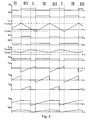
Im Folgenden wird der Betrieb des in
In der Phase 1 ist der untere Halbleiterschalter S2 der Eingangshalbbrücke 201 ausgeschaltet. Der obere Halbleiterschalter S1 der Eingangshalbbrücke 201 ist eingeschaltet. Die Ausgangshalbbrücke 202 befindet sich im umgekehrten Schaltzustand. Hier ist der obere Halbleiterschalter S3 geschlossen, während der untere Halbleiterschalter S4 geöffnet ist. Der Koppelschalter S5 ist in der Phase I geschlossen, wodurch die Eingangsstufe 213 und die Ausgangsstufe 211 in der Phase I unabhängig voneinander arbeiten.In
In der Eingangshalbbrücke 201 fließt der Strom iL1, getrieben durch die Induktivität L1, über den eingeschalteten Halbleiterschalter S1 gegen die Spannung UDC, die, wie zuvor erwähnt, größer als die Eingangsspannung UE ist. Dabei nimmt der Strom iL1 ab und kehrt schließlich seine Richtung um, so dass er negativ wird und schließlich seinen Minimalwert iL1,min erreicht. Die Steigung des Stroms iL1 beträgt während der Phase I diL1/dt = (UE - UDC)/L1. Die antiparallel zu dem Halbleiterschalter S1 geschaltete Freilaufdiode D1 befindet sich im leitenden Zustand solange der Strom iL1 positiv ist.In the
In der Ausgangsstufe 202 fließt der Strom iL2 in der Phase I durch die Induktivität L2, getrieben über den eingeschalteten Halbleiterschalter S4, und nimmt ausgehend von seinem Maximalwert iL2,max ab. Die negative Steigung des Stroms iL2 in der Phase I beträgt diL2/dt = -UA/L2. Die antiparallel zu dem Halbleiterschalter S4 geschaltete Diode D4 befindet sich in der Phase I im leitfähigen Zustand, da der Strom iL2 positiv ist.In the
Am Ende der Phase I schaltet der Halbleiterschalter S1 den Strom iL1 an seinem negativen Minimalwert iL1,min ab. Dies geschieht mit geringen Schaltverlusten, da der Abschaltvorgang durch die Kapazitäten C1, C2 und C5 entlastet wird. Nach dem Abschalten des Halbleiterschalters S1 lädt der negative Strom iL1 die Kapazitäten C1, C2 und C5 während der Kommutierungsphase um. Dadurch sinkt das elektrische Potenzial am Mittelpunkt M1 der Eingangshalbbrücke 201 auf den Wert des elektrischen Potenzials der unteren Spannungsschiene 204, so dass die Spannung über dem Halbleiterschalter S2 auf den Wert Null sinkt. Ist dieser erreicht, geht die antiparallel zu dem Halbleiterschalter S2 geschaltete Diode D2 in den leitenden Zustand über, und der Halbleiterschalter S2 kann weich eingeschaltet werden. Gleichfalls kann der Koppelschalter S5 zu diesem Zeitpunkt weich eingeschaltet werden, da die Spannung über dem Koppelschalter S5 ebenfalls den Wert Null erreicht hat. In einer Ausführungsform erfolgt das Einschalten des Koppelschalters S5 und des Halbleiterschalters S2 daher synchron. In einer weiteren Ausführungsform wird der Koppelschalter S5 mit einer geringen Verzögerung eingeschaltet. Hierdurch wird auch dann sichergestellt, dass die Spannung über dem Koppelschalter S5 beim Einschalten den Wert Null erreicht hat, wenn der Halbleiterschalter S2 aufgrund einer ungenauen Ansteuerung zu früh eingeschaltet worden ist. Die Schaltzustände der Halbleiterschalter S3 und S4 der Ausgangshalbbrücke 202 werden während der Übergangsphase I → II nicht verändert.At the end of phase I, the semiconductor switch S1 switches off the current i L1 at its negative minimum value i L1, min . This is done with low switching losses, since the switch-off is relieved by the capacitors C1, C2 and C5. After switching off the semiconductor switch S1, the negative current i L1 charges the capacitances C1, C2 and C5 during the commutation phase. As a result, the electrical potential at the midpoint M1 of the input half-
In der Phase II ist der obere Halbleiterschalter S1 der Eingangshalbbrücke 201 ausgeschaltet, und der untere Halbleiterschalter S2 ist eingeschaltet. Der Schaltzustand der Ausgangsstufe 202 hat sich gegenüber der Phase I nicht verändert, so dass sich die Eingangshalbbrücke 201 und die Ausgangshalbbrücke 202 in der Phase II in demselben Schaltzustand befinden. Der Koppelschalter S5 wird in der Phase II im leitenden Zustand betrieben.In phase II, the upper semiconductor switch S1 of the input half-
Der Eingangsstrom iL1 nimmt in der Phase II ausgehend von seinen Minimalwert iL1,min, zu und erreicht am Ende der Phase II seinen maximalen Wert iL2,max. Die Steilheit des Stroms iL1 während der Phase II beträgt diL1/dt = UE/L1. Der Strom iL2 nimmt in der Phase II weiter ab, und erreicht am Ende der Phase II seinen minimalen Wert iL2,min. Die Steigung des Stroms iL2 beträgt dabei wie in Phase I diL2/dt = -UA/L2. Am Mittelpunkt M1 der Eingangshalbbrücke 201 verzweigt sich der Strom iL1 in einen Zweig, in dem er über den oberen Halbleiterschalter S2 fließt, und einen Zweig, in dem er über den Koppelschalter S5 in den Mittelpunkt M2 der Ausgangsstufe 202 fließt. Dabei wird der Betrag der Stromstärke iS4 des durch den Halbleiterschalter S4 fließenden Stroms um den Betrag des durch den Koppelschalter S5 fließenden Stroms iS5 reduziert. Wie aus dem Diagramm in
Am Ende der Phase II werden die oberen Halbleiterschalter S2 und S4 der Eingangshalbbrücke 201 und der Ausgangshalbbrücke 202 ausgeschaltet. Die parallel zu den Halbleiterschaltern S1-S4 geschalteten Kapazitäten C1-C4 entlasten den Abschaltvorgang und ermöglichen ein weiches Ausschalten der Halbleiterschalter S2 und S4. Während der folgenden Kommutierungsphase II → III lädt der Strom iL1 - iL2 die Kapazitäten C1-C4 um. Dabei wird die Kapazität C1, wie zuvor erläutert, entladen, und die Kapazität C2 wird aufgeladen. Gleichermaßen wird die Kapazität C3 entladen, und die Kapazität C4 aufgeladen. Hierdurch steigt das elektrische Potenzial am Mittelpunkt M1 der Eingangshalbbrücke 201 beziehungsweise am Mittelpunkt M2 der Ausgangsstufe 202 auf das elektrische Potenzial der oberen Spannungsschiene 204,d.h., auf das obere Zwischenkreispotenzial. Wenn dieses erreicht ist, gehen die antiparallel zu dem Halbleiterschalter S1 geschaltete Diode D1 sowie die antiparallel zu dem Halbleiterschalter S3 geschaltete D3 in den leitenden Zustand über und die Halbleiterschalter S1 und S3 können durch ein Nullspannungsschalten eingeschaltet werden. Der Koppelschalter S5 wird während der Übergangsphase II → III und während der nachfolgenden Phase III im leitenden Zustand belassen.At the end of phase II, the upper semiconductor switches S2 and S4 of the
In der Phase III sind die oberen Halbleiterschalter S1 und S3 der Eingangshalbbrücke 201 und der Ausgangsstufe 202 eingeschaltet, während die unteren Halbleiterschalter S2 und S4 ausgeschaltet sind. Der Koppelschalter S5 ist in der Phase III geöffnet.In phase III, the upper semiconductor switches S1 and S3 of the input half-
Der Strom iL1 nimmt in der Phase III, ausgehend von seinem Maximalwert iL1,max, ab. Wie in der Phase I geschieht dies mit der negativen Steigung diL1/dt = (UE - UDC)/L1. Der Strom iL2 steigt in der Phase III ausgehend von seinem Minimalwert iL2,min auf seinen Maximalwert iL2,max. Die Steilheit des Stroms iL2 beträgt dabei diL2/dt = (UDC - UA)/L2. Wie dem Diagramm in
Am Ende der Phase III werden der obere Halbleiterschalter S3 der Ausgangshalbbrücke 202 sowie der Koppelschalter S5 ausgeschaltet. Der Ausschaltvorgang wird durch die parallel zu den Halbleiterschaltern S3 und S4 der Ausgangshalbbrücke 202 geschalteten Kapazitäten C3 und C4 und die parallel zu dem Koppelschalter S5 geschaltete Kapazität C5 entlastet, wodurch ein weiches Ausschalten des Halbleiterschalters S3 erreicht wird. Während der Kommutierungsphase III → I lädt der positive Strom iL2 die Kapazitäten C3 und C4 sowie C5 um, so dass das elektrische Potenzial am Mittelpunkt M2 der Ausgangshalbbrücke 202 auf das elektrische Potenzial der unteren Spannungsschiene 204 absinkt. Dabei wird die Kapazität C4 entladen, und die Kapazitäten C3 und C5 werden aufgeladen. Erreicht die Spannung über dem Halbleiterschalter S4 den Wert Null, geht die antiparallel zu dem Halbleiterschalter S4 geschaltete Diode D4 in den leitenden Zustand über und der Halbleiterschalter S4 kann durch Nullspannungsschalten eingeschaltet werden. Der obere Halbleiterschalter S1 der Eingangshalbbrücke 201 bleibt während der Übergangsphase III → I eingeschaltet und der untere Halbleiterschalter S2 der Eingangsstufe bleibt ausgeschaltet. Somit ist der Gleichstromsteller nach dem Einschalten des Halbleiterschalters S4 in die zuvor bereits beschriebene Phase I übergegangen.At the end of phase III, the upper semiconductor switch S3 of the output half-
Wie aus der vorangegangenen Darstellung der Funktionsweise des in der
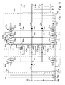
Zusätzlich oder alternativ ist es auch möglich, den Halbleiterschalter S1 und die antiparallel geschaltete Freilaufdiode D1 durch eine Diode D1' zu ersetzen, wie dies in dem Schaltbild in
Beim zuvor beschriebenen Betrieb des in der ![]()
![]()
Ein Betrieb der Eingangshalbbrücke 201 nach dem Resonant-Pole-Verfahren ist hierbei entsprechend Gleichung (4) gewährleistet, wenn gilt: ![]()
![]()
Gleichfalls kann an einem Arbeitspunkt die Situation eintreten, dass der bei der Kommutierung des Stroms iL2 von dem oberen Halbleiterschalter S3 der Ausgangshalbbrücke 202 auf den unteren Halbleiterschalter S4 der Ausgangshalbbrücke 202 auftretende Maximalwert iL2,max des Stroms iL2 nicht ausreichend positiv ist, um die Kapazitäten C3 und C4 derart umzuladen, dass die Spannung über dem einzuschaltenden Halbleiterschalter S4 auf den Wert Null sinkt. In diesem Fall, der im Folgenden als Fall 2 bezeichnet wird, muss der Strom iL1 bei diesem Kommutierungsvorgang über den Koppelschalter S5 zum Mittelpunkt M2 der Ausgangshalbbrücke 202 geführt werden, um den Kommutierungsvorgang zu unterstützen und ein Einschalten des Halbleiterschalters S4 durch Nullspannungsschalten zu ermöglichen. Um dies unter Beachtung der in Gleichung (6) angegebenen Ansteuerungsregel für den Koppelschalter S5 zu erreichen, wird in diesem Fall die Kommutierung des Stroms iL2 von dem oberen Halbleiterschalter S3 der Ausgangshalbbrücke 202 auf den unteren Halbleiterschalter S4 mit der Kommutierung des Stroms iL1 von dem oberen Halbleiterschalter S1 der Eingangshalbbrücke 201 auf den unteren Halbleiterschalter S2 synchronisiert. Der das erforderliche Umladen der Kapazitäten C1-C4 bewirkende Strom iL1 - iL2, der während dieser Kommutierungsphase näherungsweise den Wert iL1, min-iL2,max annimmt, muss dabei ausreichend negativ sein, um die parallel zu den unteren Halbleiterschaltern S2 und S4 geschalteten Kapazitäten C2 und C4 zu entladen und die parallel zu den oberen Halbleiterschaltern S1 und S3 geschalteten Kapazitäten C1 und C3 aufzuladen. Dafür muss der Minimalwert iL1,min des Stroms iL1 ausreichend kleiner sein als der Maximalwert iL2,max des Stroms iL2. Näherungsweise muss insbesondere gelten: ![]()
![]()
Um einen Betrieb der Eingangshalbbrücke 201 nach dem Resonant-Pole-Verfahren sicherzustellen, muss näherungsweise gelten: ![]()
![]()
Die zuvor am Beispiel eines Gleichstromstellers beschriebene Kopplung zwischen einer Eingangshalbbrücke 201 und einer Ausgangshalbbrücke 202 über einen Koppelschalter S5 kann mit denselben Vorteilen auch in Wechselrichterschaltungen und anderen Stromrichterschaltungen eingesetzt werden.The coupling between an input half-
In
Die Ausgangsstufe 211 der Wechselrichterschaltung umfasst in dieser Ausgestaltung drei parallel geschaltete Ausgangshalbbrücken 202a..c, die zwischen die oberen Spannungsschiene 203 und die untere Spannungsschiene 204 parallel zu der Zwischenkreiskapazität CDC geschaltet werden können. Die Ausgangshalbbrücken 202a..c umfassen dabei jeweils einen oberen Halbleiterschalter S3x und einen unteren Halbleiterschalter S4x, zwischen denen der Mittelpunkt M2x der Ausgangshalbbrücke 202x liegt (x = a,b,c). Die Mittelpunkte M2a..c sind über jeweils eine Induktivität L2x mit einem Anschluss 212x eines dreiphasigen Stromnetzes verbunden, bei dem es sich beispielsweise um ein Drehstromnetz handeln kann. Zu den Halbleiterschaltern S3a..c und S4a..c der Ausgangshalbbrücken sind Freilaufdioden D3a..c und D4a..c antiparallel sowie Kapazitäten C3a..c und C4a..c parallel geschaltet. Zur Glättung der Ausgangsspannungen U1, U2 und U3 sind Glättungskapazitäten CAa..c vorgesehen, die bei der dargestellten Ausgestaltung der Schaltungsanordnung mit der unteren Spannungsschiene 204 verbunden sind.In this embodiment, the
Die Eingangsstufe 213 besteht ebenfalls aus drei parallel geschalteten Eingangshalbbrücken 201 a..c, die zwischen die obere Spannungsschiene 203 und die untere Spannungsschiene 204 geschaltet sind. Die Eingangshalbbrücken 201a..c umfassen jeweils den oberen Halbleiterschalter S1x und den unteren Halbleiterschalter S2x, wobei zu den Halbleiterschaltern S1x und S2x Freilaufdioden D1x und D2x antiparallel sowie Kapazitäten C1x und C2x parallel geschaltet sind (x = a,b,c). Die zwischen den Halbleiterschaltern S1a..c und S2a..c liegenden Mittelpunkte M1a..c der Eingangshalbbrücken 201a..c sind jeweils über eine Induktivität L1x mit dem Pol 205 der Eingangsspannung UE verbunden. Die untere Spannungsschiene 204 ist mit dem zweiten Pol 206 der Eingangsspannung UE verbunden. Zur Stützung der Eingangsspannung UE ist eine Kapazität CE vorgesehen.The
Die Mittelpunkte M1 a..c der Eingangshalbbrücken 201 a..c sind jeweils über einen Koppelschalter S5x mit parallel geschalteter Kapazität C5x mit dem Mittelpunkt M2x einer zugeordneten Ausgangshalbbrücke 205x verbunden. Die Koppelschalter S5x sind bei der in der
Es ist ersichtlich, dass sich die in der
Um ein weiches Schalten der Eingangshalbbrücken und der Ausgangshalbbrücken zu gewährleisten, erfolgt eine Ansteuerung für den Halbleiterschalter S5x zwischen einer Eingangshalbbrücke 201x und der zugeordneten Ausgangshalbbrücke 202x analog zu Gleichung (6) gemäß: ![]()
![]()
Die Synchronisierung der Eingangshalbbrücke 201 x und der zugeordneten Ausgangshalbbrücke 202x erfolgt ebenfalls in der zuvor beschriebenen Weise, um zu gewährleisten, dass die Halbleiterschalter S3x und S4x der Ausgangshalbbrücke durch Nullspannungsschalten eingeschaltet werden können. Die Frequenzen der Eingangshalbbrücken 201 a..c und der Ausgangshalbbrücken 202a..c sind vorzugsweise gleich gewählt, und/oder die Frequenz der Ausgangshalbbrücken 202a..c wird so gewählt, dass die Frequenz der Eingangshalbbrücken 201 a..c ein ganzzahliges Vielfaches der Frequenz der Ausgangshalbbrücken 202a..c ist. Dabei können jedoch die Perioden der Ausgangshalbbrücken 201a..c, die benachbarten Phasen der dreiphasigen Ausgangsspannung speisen, bzw. die Perioden der zugeordneten Eingangshalbbrücken 201a..c, um das Drittel einer Periodendauer, d.h. um 120° in der Phase, gegeneinander verschoben werden, um die Spitzenbelastung der Zwischenkreiskapazität zu reduzieren.The synchronization of the input half-bridge 201 x and the associated output half-bridge 202 x also takes place in the manner described above in order to ensure that the semiconductor switches S3 x and S 4 x of the output half-bridge can be switched on by zero-voltage switching. The frequencies of the input half bridges 201 a..c and the output half bridges 202 a... C are preferably chosen to be the same, and / or the frequency of the output half bridges 202 a... C is selected such that the frequency of the input half bridges 201 a. C is an integer multiple of Frequency of the output half-
Die näherungsweise erforderlichen Minimal- und Maximalwerte der Eingangsströme iL1a..c der Eingangshalbbrücken 201 a..c ergeben sich durch Kombination der Gleichungen (7)-(10) zu 

Diese Werte können insbesondere unter Verwendung von Gleichung (5) durch geeignete Wahl der Frequenzen der Eingangshalbbrücken 201 a..c bzw. der Ausgangshalbbrücken 202a..c eingestellt werden. Die oberen Zeilen der in den Gleichungen (12) und (13) vorgenommenen Fallunterscheidungen gelten für den zuvor beschriebenen Fall 1 und die unteren Zeilen für den zuvor beschriebenen Fall 2.These values can be adjusted in particular using equation (5) by suitably selecting the frequencies of the input half bridges 201 a..c and the output half bridges 202 a... C. The upper lines of the case discriminations made in equations (12) and (13) apply to the above-described
Beispielhaft sind in
In den Bereichen A arbeiten die Ausgangshalbbrücke 202x und die zugeordnete Eingangshalbbrücke 201 x entsprechend dem zuvor beschriebenen Fall 1. Im Bereich B erfolgt aufgrund eines kleinen Wertes von iL2,max eine Ansteuerung entsprechend des zuvor genannten Falls 2. Daher sinkt im Bereich B der mittlere Wert des Eingangsstroms iL1x und wird an dem betrachteten Arbeitspunkt kurzzeitig sogar negativ. Hierdurch wird die Effizienz der Energieübertragung von der Eingangshalbbrücke 201 x zu der Ausgangshalbbrücke 202x verringert.In the areas A, the output half-bridge 202x and the associated input half-bridge 201 x operate in accordance with the previously described
Dies kann durch die an sich bekannte, so genannte 120°-Flattop-Modulation verhindert werden, die beispielsweise in H. van der Broeck, "Analysis of Harmonics in Voltage Fed Inverter Drives caused by PWM Schemes with Discontinuous Switching Operation", EPE, Firenze, 1991 beschrieben wird. Die 120°-Flattop-Modulation zeichnet sich dadurch aus, dass jeweils eine Ausgangshalbbrücke 202x für ein Drittel der Periodendauer der Ausgangsspannungen bzw. - ströme des Wechselrichters nicht geschaltet wird, sondern entweder der obere Halbleiterschalter S3x dieser Ausgangshalbbrücke 202x eingeschaltet wird und den Mittelpunkt M2x dieser Ausgangshalbbrücke 202x mit der oberen Spannungsschiene 203 verbindet, oder der untere Halbleiterschalter S4x dieser Ausgangshalbbrücke 202x eingeschaltet ist und den Mittelpunkt M2x der Ausgangshalbbrücke M2x mit der unteren Spannungsschiene 204 verbindet. Als diejenige Ausgangshalbbrücke 202x, die nicht geschaltet wird, wird dabei jeweils die Ausgangshalbbrücke 202x gewählt, welche die kleinste Strangspannung liefert. Dies entspricht der Wahl eines minimal Nullsystems.This can be prevented by the well-known, so-called 120 ° flattop modulation described, for example, in H. van der Broeck, "Analysis of Harmonics in Voltage Fed Inverter Drives caused by PWM Schemes with Discontinuous Switching Operation", EPE, Firenze , 1991. The 120 ° flattop modulation is characterized in that in each case one output half bridge 202x is not switched for one third of the period of the output voltages or currents of the inverter, but either the upper semiconductor switch S3x of this output half bridge 202x is turned on and the center M2x of these Output half-bridge 202x connects to the
Durch eine pulsdauermodulierte Ansteuerung der Ausgangshalbbrücken 202a..c der Wechselrichterschaltung entsprechend der 120°-Flattop-Modulation wird das zuvor genannte Problem weitgehend vermieden, und die Effizienz der Energieübertragung erhöht. Grund hierfür ist, dass der zuvor genannte Fall 2 bei einer derartigen Modulation nur für eine kurze Zeitdauer während Periodendauer der Ausgangsspannungen Ux bzw. Ausgangsströme iL2x auftritt. Während des weit überwiegenden Teils der Periodendauer, in dem der Fall 2 für eine Ausgangshalbbrücke 202x eintreten würde, muss diese Halbbrücke nämlich nicht geschaltet werden. Beispielhaft wird dies in dem Diagramm in der
Während der Ansteuerung der Ausgangshalbbrücke 202x und der zugehörigen Eingangshalbbrücke 201 x gemäß dem Fall 2, würde der Ladestrom iL1x der Zwischenkreiskapazität CDC absinken, was durch eine geeignete Regelung verhindert wird.During the activation of the output half bridge 202x and the associated input half bridge 201x according to the
Bei einer Ansteuerung der Ausgangshalbbrücken 202a..c gemäß des 120°-Flattop-Verfahrens kommt es, wie zuvor erläutert, nur zu kurzeitigen Einbrüchen des. Diese werden in einer Ausgestaltung durch eine kurzzeitige Erhöhung des mittleren Eingangsstroms iL1y der übrigen Eingangshalbbrücke 201y kompensiert. Für diese Ausgestaltung sind in dem Diagramm in
Bei einer Ansteuerung der Ausgangshalbbrücke 202x und der zugehörigen Eingangshalbbrücke 201x gemäß dem Fall 2 muss über den Koppelschalter S5x ein Strom vom Mittelpunkt M2x der Ausgangshalbbrücke 202x zum Mittelpunkt M1x der Eingangshalbbrücke 201x geführt werden, während der bei einem Betrieb gemäß dem Fall 1 über den Koppelschalter 205x geführte Strom von dem Mittelpunkt M1x der Eingangshalbbrücke 205 in den Mittelpunkt M2x der Ausgangshalbbrücke 202x fließt. Da bei einer Ansteuerung der Wechselrichterschaltung nach dem 120°-Flattop-Verfahren nur kurzzeitig ein Betrieb gemäß Fall 2 erforderlich ist, um ein weiches Schalten der Ausgangshalbbrücke 202x zu gewährleisten, werden in einer Ausführungsform der Wechselrichterschaltung unidirektionale Koppelschalter S5'a...c eingesetzt. Eine entsprechende Schaltungsanordnung mit ausgangsseitigem Wechselrichter und unidirektionalen Koppelschaltern S5'a..c ist dabei in
Eine weitere Ausgestaltung einer Wechselrichterschaltungsanordnung ist in
Die Frequenzen, mit denen die Eingangshalbbrücke 201 und die Ausgangshalbbrücken 202a..c bei der in der
Der einer Ausgangshalbbrücke 202x zugeordnete Koppelschalter S5x wird bei positivem Ausgangsstrom iL2x der Ausgangshalbbrücke 202x dann im leitenden Zustand betrieben, wenn der Ausgangsstrom iL2x der Ausgangshalbbrücke 202x von der unteren Spannungsschiene 204 auf die obere Spannungsschiene 203 kommutiert. Hierdurch wird ein weiches Einschalten des oberen Halbleiterschalters S3x und ein weiches Ausschalten des unteren Halbleiterschalters S4x gewährleistet. Bei negativem Ausgangsstrom iL2x der Ausgangshalbbrücke 202x wird der zugeordnete Koppelschalter S5x dann im leitenden Zustand betrieben, wenn der Ausgangsstrom iL2x der Ausgangshalbbrücke 202x von der oberen Spannungsschiene 203 auf die untere Spannungsschiene 204 kommutiert, um ein weiches Einschalten des unteren Halbleiterschalters S4x und ein weiches Ausschalten des oberen Halbleiterschalters S3x zu gewährleisten. Die durch den Koppelschalter S5x fließenden Ströme haben in den beiden zuvor genannten Fällen verschiedene Vorzeichen, daher sind im vollständig weich schaltenden Betrieb des aus den Ausgangshalbbrücken 202a..c bestehenden Wechselrichters bidirektionale Koppelschalter S5a..c erforderlich.The coupling switch S5x assigned to an output half-bridge 202x is operated in a conducting state when the output half-bridge 202x has a positive output current i L2x , when the output current i L2x of the output half-bridge 202x commutes from the
Eine Synchronisierung der Ausgangshalbbrücken 202a..c und der Eingangshalbbrücke 201 wird bei der in der
In
Die Eingangsstufe 213 der Wechselrichterschaltungsanordnung umfasst zwei parallel geschaltete Eingangshalbbrücken 201a,b des zuvor beschriebenen Typs, die zwischen die obere Spannungsschiene 203 und die untere Spannungsschiene 204 parallel zu der Zwischenkreiskapazität CDC geschaltet sind. Die Mittelpunkte M1a..c der Eingangshalbbrücken sind jeweils über eine Induktivität L1a,b mit einem Pol 205, 206 einer Eingangsspannung UE verbunden. Zur Stützung der Eingangsspannung UE ist wiederum eine parallel zu der Eingangsspannung UE geschaltete Kapazität CE vorgesehen.The
Die Eingangshalbbrücke 201 a, deren Mittelpunkt M1 a mit dem auf höherem elektrischen Potenzial liegenden Pol 205 der Eingangsspannung UE verbunden ist, arbeitet bei der dargestellten Schaltungsanordnung im Hochsetzstellerbetrieb, während die Eingangshalbbrücke 201a, deren Mittelpunkt M1b mit dem anderen Pol 206 der Eingangsspannung UE verbunden ist, im Tiefsetzstellerbetrieb arbeitet. Beide Eingangshalbbrücken 201 a, 201 b werden in der zuvor beschriebenen Weise nach dem oben beschriebenen Resonant-Pole-Verfahren betrieben. Um Leistung in den aus der Zwischenkreiskapazität bestehenden Zwischenkreis einzuspeisen, ist dabei der Eingangsstrom iL1a der Eingangshalbbrücke 201a im Mittel positiv und der Eingangsstrom iL2b der Eingangshalbbrücke 201 b im Mittel negativ. Durch eine geeignete Wahl der Induktivitäten L1a und L1 b sowie der Frequenz der Eingangshalbbrücken 201 a, 201 b wird dabei erreicht, dass der Minimalwert des Eingangsstroms iL1a, der bei der Kommutierung des Stroms iL1a von dem oberen Halbleiterschalter S1a auf den unteren Halbleiterschalter S2a der Eingangshalbbrücke 201 a vorliegt, ausreichend negativ ist, um den unteren Halbleiterschalter S2a durch Nullspannungsschalten einzuschalten. Ferner wird der Maximalwert des Stroms iL1b, der bei der Kommutierung des Stroms iL1b von dem unteren Halbleiterschalter 201 b auf den oberen Halbleiterschalter 202b vorliegt, so eingestellt, dass er ausreichend positiv wird, um ein Einschalten des oberen Halbleiterschalters S1b durch Nullspannungsschalten zu ermöglichen. Die Richtungen der Ströme werden dabei so gewählt, wie in der
Über ein Koppelnetzwerk 222 sind die Mittelpunkte M2a..c der Ausgangshalbbrücken 202a..c mit den Mittelpunkten M1 a,b der Eingangshalbbrücken 201 a..b verbunden. Das Koppelnetzwerk 222 ist so aufgebaut, dass die Mittelpunkte M2a..c der Ausgangshalbbrücken 202a..c jeweils mit dem Mittelpunkt M1a der im Hochsetzstellerbetrieb arbeitenden Eingangshalbbrücke 201a über einen unidirektionalen Koppelschalter S51x (x= a, b, c) verbunden sind, der im eingeschalteten Zustand einen (positiven) Stromfluss von dem Mittelpunkt M1a der Eingangshalbbrücke 201 a in den Mittelpunkt M2x der betreffenden Ausgangshalbbrücke 202x ermöglicht. Ferner sind die Mittelpunkte M2a..c der Ausgangshalbbrücken 202a..c jeweils mit dem Mittelpunkt M1b der im Tiefsetzstellerbetrieb arbeitenden Eingangshalbbrücke 201 b über einen unidirektionalen Koppelschalter S52x (x= a, b, c) verbunden, der im eingeschalteten Zustand einen (positiven) Stromfluss von dem Mittelpunkte M2x der betreffenden Ausgangshalbbrücke 202x in den Mittelpunkt M1a der Eingangshalbbrücke 201 b ermöglicht. Die parallel zu den Koppelschaltern S51 a..c und S52a..c geschalteteten Kapazitäten sind aus Gründen der Übersichtlichkeit in
Die Frequenzen, mit denen die Eingangshalbbrücken 201 a,b und die Ausgangshalbbrücken 202a..c geschaltet werden, werden gleich gewählt. Ferner sind die Perioden der Eingangshalbrücken 201a,b und der Ausgangshalbbrücken 202a..c vorzugsweise synchronisiert.The frequencies at which the input half-
Die im Hochsetzstellerbetrieb arbeitende Eingangshalbbrücke 201 a ist insbesondere dazu in der Lage, dem Mittelpunkt M2x einer Ausgangshalbbrücke 202x Strom zuzuführen. Daher wird eine Ausgangshalbbrücke 202x im Zusammenwirken mit der Eingangshalbbrücke gemäß dem zuvor beschriebenen Fall 1 betrieben, wenn der Strom iL2x bei der Kommutierung von dem unteren Halbleiterschalter S4x auf den oberen Halbleiterschalter S3x nicht ausreichend negativ ist, um die Kapazitäten C3x und C4x derart umzuladen, dass die Spannung über dem einzuschaltenden Halbleiterschalterschalter S3x auf den Wert Null sinkt, der für ein weiches Einschalten erforderlich wäre. Solange dies der Fall ist, wird der Koppelschalter in einer Ausgestaltung S51x entsprechend der Gleichung ![]()
betrieben. Der Koppelschalter S52x bleibt geschlossen, solange die zuvor genannte Bedingung erfüllt ist. Die zuvor genannte Kommutierung ist dabei mit der Kommutierung des Eingangsstroms iL1a der Eingangshalbbrücke von dem unteren Halbleiterschalter S2a auf den oberen Halbleiterschalter S1a bzw. die entsprechende Diode synchronisiertThe operating in Hochsetzstellerbetrieb operating input half-![]()
operated. The coupling switch S52x remains closed as long as the aforementioned condition is met. The aforementioned commutation is synchronized with the commutation of the input current i L1a of the input half-bridge from the lower semiconductor switch S2a to the upper semiconductor switch S1a or the corresponding diode
Die im Tiefsetzstellerbetrieb arbeitende Eingangshalbbrücke 201 b ist insbesondere dazu in der Lage, Strom vom Mittelpunkt M2x einer Ausgangshalbbrücke 202x abzuführen. Daher wird eine Ausgangshalbbrücke 202x im Zusammenwirken mit der Eingangshalbbrücke gemäß dem zuvor beschriebenen Fall 2 betrieben, wenn der bei der Kommutierung des Stroms iL2x von dem oberen Halbleiterschalter S3x der Ausgangshalbbrücke 202x auf den unteren Halbleiterschalter S4x der Ausgangshalbbrücke 202x auftretende Maximalwert iL2,max des Stroms iL2x nicht ausreichend positiv ist, um die Kapazitäten C3 und C4 derart umzuladen, dass die Spannung über dem einzuschaltenden Halbleiterschalter S4 auf den Wert Null sinkt. Solange dies der Fall ist, wird der Koppelschalter S52x entsprechend der Gleichung ![]()
betrieben. Der Koppelschalter S52x bleibt geschlossen, solange die zuvor genannte Bedingung erfüllt ist. Die zuvor genannte Kommutierung ist dabei mit der Kommutierung des Eingangsstroms iL1b der Eingangshalbbrücke 201 b von dem oberen Halbleiterschalter S1a auf den unteren Halbleiterschalter S2a bzw. die entsprechende Diode synchronisiert.The input half-![]()
operated. The coupling switch S52x remains closed as long as the aforementioned condition is met. The aforementioned commutation is synchronized with the commutation of the input current i L1b of the
Der in der
Den zuvor dargestellten Wechselrichterschaltungen ist gemeinsam, dass sie aufgrund der weich schaltenden Betriebsmodi eine sehr effiziente Energieübertragung ermöglichen. Ferner kann die Eingangsspannung in einem sehr weiten Bereich variiert werden. Daher eignen sie sich besonders gut für die Einspeisung einer in einem Photovoltaikgenerator, einer Brennstoffzelle oder einer Windkraftanlage erzeugten Energie in ein Stromnetz. Gleichfalls kann die Schaltung auch durch einen Generator oder Batterie gespeist werden. Vorteilhaft kann mit der Schaltungsanordnung insbesondere ein Motor, beispielsweise ein Synchron- oder Asynchronmotor, mit Energie versorgt werden.The inverter circuits described above have in common that they allow a very efficient energy transfer due to the soft-switching operating modes. Furthermore, the input voltage can be varied within a very wide range. Therefore, they are particularly well suited for the feeding of a generated in a photovoltaic generator, a fuel cell or a wind turbine power into a power grid. Likewise, the circuit can also be powered by a generator or battery. Advantageously, with the circuit arrangement, in particular a motor, for example a synchronous or asynchronous motor, be supplied with energy.
Bei Verwendung von bidirektionalen Koppelschaltern können die Schaltungsanordnungen bidirektional betrieben werden, d.h., Leistung kann sowohl von der Ausgangsstufe zur Eingangsstufe als auch umgekehrt transportiert werden. Vorteilhaft ist die Schaltungsanordnung so ausgeführt, dass ein bidirektionaler Betrieb möglich ist. Bei einem bidirektionalen Betrieb können die Ausgangshalbbrücken, die in den zuvor beschriebenen Ausgestaltungen als Wechselrichter arbeiten, als Gleichrichter betrieben werden.When bidirectional coupling switches are used, the circuit arrangements can be operated bidirectionally, i.e. power can be transported both from the output stage to the input stage and vice versa. Advantageously, the circuit arrangement is designed so that a bidirectional operation is possible. In a bidirectional operation, the output half-bridges, which operate in the embodiments described above as an inverter, can be operated as a rectifier.
In
Der Fachmann erkennt zudem, dass analog zu den zuvor beschriebenen dreiphasigen Wechselrichterschaltungen einphasige Wechselrichter aufgebaut werden können. Als Beispiel ist dabei die in der
Claims (25)
- A circuit arrangement for converting an input voltage (UE) into an output voltage (UA)- comprising at least one output half-bridge (202) and at least one input half-bridge (201), which are connected in parallel to an intermediate circuit capacitor (CDC),- whereby each half-bridge (201; 202) has an upper bridge element (S1, D1; C1; D1', C1; S3, D3, C3), a lower bridge element (S2, D2; C2; S4; D4, C4; D4', C4) and an accessible midpoint (M1; M2) between the upper bridge element (S1, D1; C1; D1', C1; S3, D3, C3) and the lower bridge element (S2, D2; C2; S4; D4, C4; D4', C4), whereby the bridge elements comprise a parallel circuit of a switching element (S1, D1; D1'; S2, D2; S3, D3, S4, D4; D4') and a capacitor (C1; C2; C3; C4),- whereby a current (iL1; iL2) that is flowing through the midpoint (M1; M2) of a half-bridge (201; 202) can be commutated from the lower bridge element to the upper bridge element and vice versa by switching at least one switching element of the bridge elements of the half-bridge (201; 202),- whereby the midpoint (M1) of the input half-bridge (201) is connected to an input voltage terminal (205) via an input inductor (L1), and- whereby the midpoint (M2) of the output half-bridge (202) is connected to an output voltage terminal (208) via an output inductor (L2),characterized in that
the midpoint (M1) of the input half-bridge (201) is connected to the midpoint (M2) of the output half-bridge (202) via a coupling switch (S5; S5'). - The circuit arrangement according to claim 1,
characterized in that,
during a commutation of the current - which is flowing through the midpoint (M1; M2) of a half-bridge (201; 202) - from a first bridge element to the second bridge element of the half-bridge (201; 202), the bridge elements are operated in a blocking state during a commutation phase. - The circuit arrangement according to claim 1 or 2,
characterized in that,
during a commutation of an output current (iL2) - which is flowing through the midpoint (M2) of the output half-bridge (202) into the output inductor (L2) - from a first bridge element to a second bridge element of the output half-bridge (202), the coupling switch (S5; S5') is switched on if the output current (iL2) is not suitable in terms of its magnitude and/or its sign to cause a discharging of the capacitor (C3; C4) of the second bridge element. - The circuit arrangement according to claim 3,
characterized in that
an input current (iL1) that is flowing through the input inductor (L1) into the midpoint (M1) of the input half-bridge (201) during the commutation is adjusted in such a way that the difference between this input current (iL1) and the output current (iL2) is suitable in terms of its magnitude and/or its sign to cause a discharging of the capacitor (C3; C4) of the second bridge element. - The circuit arrangement according to one of the preceding claims,
characterized in that
the coupling switch (S5') is switched off when the upper bridge element (S1, D1; C1; D1', C1) of the input half-bridge (201) as well as the lower bridge element (S4; D4, C4; D4', C4) of the output half-bridge (202) are in a conductive state, or when the lower bridge element (S2, D2; C2) of the input half-bridge (201) as well as the upper bridge element (S3, D3, C3) of the output half-bridge (202) are in a conductive state. - The circuit arrangement according to one of the preceding claims,
characterized in that
the coupling switch (S5, S5') is only switched on when the upper bridge elements (S1, D1; C1; D1', C1; S3, D3, C3) of the input half-bridge (201) and of the output half-bridge (202) are in a conductive state or in a blocking state. - The circuit arrangement according to one of the preceding claims,
characterized in that
a commutation of the output current (iL2) - which is flowing from the midpoint (M2) of the output half-bridge (202) into the output inductor (L2) - from a first bridge element to the second bridge element of the output half-bridge (202) during which the coupling switch (S5; S5') is switched on, is synchronized with the commutation of the input current (iL1) - which is flowing from the input inductor (L1) into the midpoint (M1) of the input half-bridge (201) - from a first bridge element to the second bridge element of the input half-bridge (201) during which the input current (iL1) is adjusted in such a way that the difference between the input current (iL1) and the output current (iL2) is suitable in terms of its magnitude and its sign to cause a discharging of the capacitor (C3; C4) of the second bridge element. - The circuit arrangement according to one of the preceding claims,
characterized in that
a current that is flowing from the input inductor (L1) into the input half-bridge (201) is adjusted in such a way that, during the commutation from a first bridge element to a second bridge element of the input half-bridge (201), it is suitable in terms of its magnitude and/or its sign to cause a discharging of the capacitor (C1; C2) of the second bridge element during the commutation phase. - The circuit arrangement according to one of the preceding claims,
characterized in that
the output half-bridge (202) is clocked at a frequency that is the same as the frequency of the input half-bridge (201), and/or in that the frequency of the input half-bridge (201) is an integer multiple of the frequency of the output half-bridge (202). - The circuit arrangement according to one of the preceding claims,
characterized in that
several output half-bridges (202; 202a...c) that are electrically connected in parallel to the intermediate circuit capacitor (CDC) are provided which are operated as single-phase or multi-phase inverters. - The circuit arrangement according to claim 10,
characterized in that
a bidirectional operation is provided, whereby the output half-bridges (202; 202a...c; 202a,b) can be operated in one mode of operation as rectifiers. - The circuit arrangement according to one of the preceding claims,
characterized in that
the number of input half-bridges (201) corresponds to the number of output half-bridges (202), whereby the midpoints (M2) of the output half-bridges (202) are each connected to precisely one midpoint (M1) of an input half-bridge (201) via a coupling switch (S5; S5'). - The circuit arrangement according to one of the preceding claims,
characterized in that
the midpoints (M1) of the input half-bridges (201) are each connected to an input voltage terminal (205) via an input inductor (L1). - The circuit arrangement according to one of the preceding claims,
characterized in that
the output half-bridges (202) that are electrically connected in parallel to the intermediate circuit capacitor (CDC) are each connected to precisely one input half-bridge (201) via a coupling switch (S5; S5'). - The circuit arrangement according to one of the preceding claims,
characterized in that
the output half-bridges (202a... c) that form the inverter are actuated on the basis of a 120° flat-top modulation, so that the bridge elements of one output half-bridge (202a; 202b; 202c) are not switched for one-third of the period of the mean output current (iL2a1; iL2b; iL2c) of the output half-bridge (202). - The circuit arrangement according to one of the preceding claims
characterized in that
two input half-bridges (20 1 a,b) that are electrically connected in parallel to the intermediate circuit capacitor (CDC) are provided whose midpoints (M1a,b) are each connected to a pole (205; 206) of the input voltage (UE) via an input inductor (L1a,b), whereby a first input half-bridge (201a) functions in step-up converter mode and a second input half-bridge (201b) functions in step-up-converter mode, and whereby the midpoint (M2) of the output half-bridge (202) is connected to the midpoints (M1a,b) of the input half-bridges (20 1 a,b) via a coupling switch (S51; S52). - The circuit arrangement according to claim 16,
characterized in that,
during a commutation of an output current (iL2) - which is flowing through the midpoint (M2) of the output half-bridge (202) in the direction of the output inductor (L2) - from a first bridge element to a second bridge element of the output half-bridge (202), one of the coupling switches (S5; S5') is switched on if the output current (iL2) is not suitable in terms of its magnitude and/or its direction to cause a discharging of the capacitor (C3; C4) of the second bridge element. - The circuit arrangement according to claim 16 or 17,
characterized in that
the coupling switch (S51; S52) that is switched on is the one that connects the midpoint (M2) of the output half-bridge (202) to the midpoint (M1a; M1b) of the input half-bridge (201; 201b), which is selected in such a way that the input current (iL1a; iL2b) that is flowing through the input inductor (L1a; L1b) of the input half-bridge (201a, 201b) into the midpoint (M1a; M1b) of the input half-bridge (201a, 201b) during the commutation is adjusted in such a way that the difference between this input current (iL1a; iL1b) and the output current (iL2) is suitable to cause a discharging of the capacitor (C3; C4) of the second bridge element of the output half-bridge (202). - The circuit arrangement according to one of the preceding claims,
characterized in that
the input half-bridge (201) can be operated as single-phase or multi-phase rectifiers. - The circuit arrangement according to one of the preceding claims,
characterized in that
the switching element (S2; D2) of the lower bridge element of the input half-bridge (201) and the switching element (S3; D3) of the upper bridge element of the output half-bridge (202) are each a transistor with a flyback diode that is connected anti-parallel. - The circuit arrangement according to one of the preceding claims,
characterized in that
the switching element (S1; D1; D1') of the upper bridge element of the input half-bridge (201) and the switching element (S4; D4; D4') of the lower bridge element of the output half-bridge (201) [sic] are each a transistor with a flybackdiode that is connected anti-parallel or a diode that is connected in such a way that it is in a blocking state when the switching element (S2, D2; S3; D3) of the opposite bridge element is connected so as to be conductive. - The circuit arrangement according to one of the preceding claims,
characterized in that
the coupling switch (S5; S5') comprises at least one transistor whose source or emitter terminal is connected to the midpoint of the input half-bridge or of the output half-bridge, whereby a driver circuit of the transistor is fed by means of the bootstrap method. - The circuit arrangement according to one of the preceding claims,
characterized in that
the bridge elements and the coupling switches (S5; S5') are accommodated in a module. - The circuit arrangement according to claim 23,
characterized in that
a driver circuit is integrated into the module, at least partially. - A method for actuating a circuit arrangement for converting an input voltage (UE) into an output voltage (UA), comprising the steps:- connecting at least one output half-bridge (202) and at least one input half-bridge (201) in parallel to an intermediate circuit capacitor (CDC),- establishing each half-bridge (201; 202) by means of an upper bridge element (S1, D1; C1; D1', C1; S3, D3, C3), by means of a lower bridge element (S2, D2; C2; S4; D4, C4; D4', C4) and by means of an accessible midpoint (M1; M2) between the upper bridge element (S1, D1; C1; D1', C1; S3, D3, C3) and the lower bridge element (S2, D2; C2; S4; D4, C4; D4', C4),- whereby, in order to form the bridge elements, in each case, a switching element (S1, D1; D1'; S2, D2; S3, D3, S4, D4; D4') and a capacitor (C1; C2; C3; C4) are connected in parallel,- commutating a current (iL1; iL2) - which is flowing through the midpoint (M1; M2) of a half-bridge (201; 202) - from the lower bridge element to the upper bridge element and vice versa by switching at least one switching element of the bridge elements of the half-bridge (201; 202),- connecting the midpoint (M1) of the input half-bridge (201) to an input voltage terminal (205) via an input inductor (L1),- connecting the midpoint (M2) of the output half-bridge (202) to an output voltage terminal (208) via an output inductor (L2), and- connecting the midpoint (M1) of the input half-bridge (201) to the midpoint (M2) of the output half-bridge (202) via a coupling switch (S5; S5'),whereby furthermore, with this method, during a commutation of the current (iL1; iL2) - which is flowing through the midpoint (M1; M2) of a half-bridge (201; 202) - from a first bridge element to the second bridge element of the half-bridge (201; 202), the bridge elements are operated in a blocking state during a commutation phase, whereby during a commutation of an output current (iL2) - which is flowing through the midpoint (M2) of the output half-bridge (202) into the output inductor (L2) - from a first bridge element to a second bridge element of the output half-bridge (202), the coupling switch (S5; S5') is switched on if the output current (iL2) is not suitable in terms of its magnitude and/or its sign to cause a discharging of the capacitor (C3; C4) of the second bridge element.
Priority Applications (1)
| Application Number | Priority Date | Filing Date | Title |
|---|---|---|---|
| PL08000643T PL1976103T3 (en) | 2007-01-15 | 2008-01-15 | Soft switching converter and method for its operation |
Applications Claiming Priority (1)
| Application Number | Priority Date | Filing Date | Title |
|---|---|---|---|
| DE102007002874A DE102007002874A1 (en) | 2007-01-15 | 2007-01-15 | Converter architecture for low loss adjustment of double galvanically not separated voltages, has input stage and output stage formed from multiple transistor half bridges and inductances |
Publications (3)
| Publication Number | Publication Date |
|---|---|
| EP1976103A2 EP1976103A2 (en) | 2008-10-01 |
| EP1976103A3 EP1976103A3 (en) | 2011-06-15 |
| EP1976103B1 true EP1976103B1 (en) | 2013-08-07 |
Family
ID=39314428
Family Applications (1)
| Application Number | Title | Priority Date | Filing Date |
|---|---|---|---|
| EP08000643.0A Not-in-force EP1976103B1 (en) | 2007-01-15 | 2008-01-15 | Soft switching converter and method for its operation |
Country Status (5)
| Country | Link |
|---|---|
| EP (1) | EP1976103B1 (en) |
| DE (1) | DE102007002874A1 (en) |
| DK (1) | DK1976103T3 (en) |
| ES (1) | ES2434091T3 (en) |
| PL (1) | PL1976103T3 (en) |
Cited By (1)
| Publication number | Priority date | Publication date | Assignee | Title |
|---|---|---|---|---|
| US9584040B2 (en) | 2011-11-24 | 2017-02-28 | Bombardier Transportation Gmbh | Double-rectifier for a multi-phase contactless energy transmission system |
Families Citing this family (4)
| Publication number | Priority date | Publication date | Assignee | Title |
|---|---|---|---|---|
| DE102011119261A1 (en) * | 2011-11-24 | 2013-05-29 | Paul Vahle Gmbh & Co. Kg | Controlled rectifier with a B2 bridge and only one switching device |
| CN111010158B (en) * | 2019-12-11 | 2023-11-21 | 中电长城圣非凡信息系统有限公司 | Converter method and device of controllable reactor |
| DE102020124387A1 (en) | 2020-09-18 | 2022-03-24 | Bayerische Motoren Werke Aktiengesellschaft | Power electronic device, method for its operation and motor vehicle |
| CN112821791B (en) * | 2021-02-02 | 2022-08-05 | 张超 | Direct current reduces half and presses four-quadrant rectifier |
-
2007
- 2007-01-15 DE DE102007002874A patent/DE102007002874A1/en not_active Withdrawn
-
2008
- 2008-01-15 PL PL08000643T patent/PL1976103T3/en unknown
- 2008-01-15 ES ES08000643T patent/ES2434091T3/en active Active
- 2008-01-15 DK DK08000643.0T patent/DK1976103T3/en active
- 2008-01-15 EP EP08000643.0A patent/EP1976103B1/en not_active Not-in-force
Cited By (1)
| Publication number | Priority date | Publication date | Assignee | Title |
|---|---|---|---|---|
| US9584040B2 (en) | 2011-11-24 | 2017-02-28 | Bombardier Transportation Gmbh | Double-rectifier for a multi-phase contactless energy transmission system |
Also Published As
| Publication number | Publication date |
|---|---|
| EP1976103A2 (en) | 2008-10-01 |
| EP1976103A3 (en) | 2011-06-15 |
| PL1976103T3 (en) | 2014-03-31 |
| DK1976103T3 (en) | 2013-11-04 |
| ES2434091T3 (en) | 2013-12-13 |
| DE102007002874A1 (en) | 2008-07-17 |
Similar Documents
| Publication | Publication Date | Title |
|---|---|---|
| EP2515424B1 (en) | Direct current converter | |
| EP2537239B1 (en) | 3-stage pulse width modulation inverter with discharge network | |
| EP2737618B1 (en) | Electrical converter system | |
| EP3014725B1 (en) | Energy storage device having a dc voltage supply circuit and method for providing a dc voltage from an energy storage device | |
| EP2144359A2 (en) | DC/DC-converter | |
| EP2187510A1 (en) | Inverter start up switch | |
| EP2391522A2 (en) | Dc/dc converter and ac/dc converter | |
| DE102009052461A1 (en) | Inverter circuitry | |
| EP2291906B1 (en) | Inverter and method for operating the inverter | |
| DE102013212682B4 (en) | Energy storage device with DC power supply circuit and method for providing a DC voltage from an energy storage device | |
| CH698835B1 (en) | Internal power supply for converter switch driver. | |
| EP1969707A1 (en) | Circuit arrangement having a dual coil for producing alternating voltage or an alternating current | |
| EP2451065B1 (en) | Inverter circuitry comprising a buck converter | |
| EP2863528A1 (en) | Operation of an inverter as a DC/DC-converter | |
| DE102012202867A1 (en) | Charging circuit for energy storage device for electrical propulsion system used for e.g. electric car, has choke transformer and switching element controller which receive direct current for charging energy storage modules | |
| EP1976103B1 (en) | Soft switching converter and method for its operation | |
| EP2709257A2 (en) | Power converter circuit and method for controlling the power converter circuit | |
| WO2015091373A1 (en) | Method for controlling a full-bridge dc-dc converter | |
| WO2015062900A1 (en) | Charging circuit for an energy storage device and method for charging an energy storage device | |
| DE102011018357A1 (en) | DC converter | |
| DE102010060508B4 (en) | Voltage converter with a storage choke with a winding and a storage choke with two windings | |
| DE10303421A1 (en) | Current and voltage converter circuit has a primary transformer winding connected using alternate switching stages | |
| DE102013212692A1 (en) | Energy storage device with DC power supply circuit | |
| EP3120447A1 (en) | Electrical circuit comprising a half-bridge | |
| CH701856B1 (en) | A method for driving an active converter circuit and corresponding circuit. |
Legal Events
| Date | Code | Title | Description |
|---|---|---|---|
| PUAI | Public reference made under article 153(3) epc to a published international application that has entered the european phase |
Free format text: ORIGINAL CODE: 0009012 |
|
| AK | Designated contracting states |
Kind code of ref document: A2 Designated state(s): AT BE BG CH CY CZ DE DK EE ES FI FR GB GR HR HU IE IS IT LI LT LU LV MC MT NL NO PL PT RO SE SI SK TR |
|
| AX | Request for extension of the european patent |
Extension state: AL BA MK RS |
|
| PUAL | Search report despatched |
Free format text: ORIGINAL CODE: 0009013 |
|
| AK | Designated contracting states |
Kind code of ref document: A3 Designated state(s): AT BE BG CH CY CZ DE DK EE ES FI FR GB GR HR HU IE IS IT LI LT LU LV MC MT NL NO PL PT RO SE SI SK TR |
|
| AX | Request for extension of the european patent |
Extension state: AL BA MK RS |
|
| 17P | Request for examination filed |
Effective date: 20111215 |
|
| AKX | Designation fees paid |
Designated state(s): AT BE BG CH CY CZ DE DK EE ES FI FR GB GR HR HU IE IS IT LI LT LU LV MC MT NL NO PL PT RO SE SI SK TR |
|
| GRAP | Despatch of communication of intention to grant a patent |
Free format text: ORIGINAL CODE: EPIDOSNIGR1 |
|
| RIN1 | Information on inventor provided before grant (corrected) |
Inventor name: DE DONCKER, RIK W. A. A. Inventor name: RIGBERS, KLAUS |
|
| GRAS | Grant fee paid |
Free format text: ORIGINAL CODE: EPIDOSNIGR3 |
|
| GRAA | (expected) grant |
Free format text: ORIGINAL CODE: 0009210 |
|
| AK | Designated contracting states |
Kind code of ref document: B1 Designated state(s): AT BE BG CH CY CZ DE DK EE ES FI FR GB GR HR HU IE IS IT LI LT LU LV MC MT NL NO PL PT RO SE SI SK TR |
|
| REG | Reference to a national code |
Ref country code: GB Ref legal event code: FG4D Free format text: NOT ENGLISH |
|
| REG | Reference to a national code |
Ref country code: CH Ref legal event code: EP Ref country code: AT Ref legal event code: REF Ref document number: 626121 Country of ref document: AT Kind code of ref document: T Effective date: 20130815 |
|
| REG | Reference to a national code |
Ref country code: IE Ref legal event code: FG4D Free format text: LANGUAGE OF EP DOCUMENT: GERMAN |
|
| REG | Reference to a national code |
Ref country code: DE Ref legal event code: R096 Ref document number: 502008010429 Country of ref document: DE Effective date: 20131010 |
|
| REG | Reference to a national code |
Ref country code: DK Ref legal event code: T3 Effective date: 20131030 |
|
| REG | Reference to a national code |
Ref country code: CH Ref legal event code: NV Representative=s name: R.A. EGLI AND CO, PATENTANWAELTE, CH |
|
| REG | Reference to a national code |
Ref country code: SE Ref legal event code: TRGR |
|
| REG | Reference to a national code |
Ref country code: NL Ref legal event code: T3 |
|
| REG | Reference to a national code |
Ref country code: ES Ref legal event code: FG2A Ref document number: 2434091 Country of ref document: ES Kind code of ref document: T3 Effective date: 20131213 |
|
| REG | Reference to a national code |
Ref country code: NO Ref legal event code: T2 Effective date: 20130807 |
|
| REG | Reference to a national code |
Ref country code: LT Ref legal event code: MG4D |
|
| PG25 | Lapsed in a contracting state [announced via postgrant information from national office to epo] |
Ref country code: PT Free format text: LAPSE BECAUSE OF FAILURE TO SUBMIT A TRANSLATION OF THE DESCRIPTION OR TO PAY THE FEE WITHIN THE PRESCRIBED TIME-LIMIT Effective date: 20131209 Ref country code: HR Free format text: LAPSE BECAUSE OF FAILURE TO SUBMIT A TRANSLATION OF THE DESCRIPTION OR TO PAY THE FEE WITHIN THE PRESCRIBED TIME-LIMIT Effective date: 20130807 Ref country code: IS Free format text: LAPSE BECAUSE OF FAILURE TO SUBMIT A TRANSLATION OF THE DESCRIPTION OR TO PAY THE FEE WITHIN THE PRESCRIBED TIME-LIMIT Effective date: 20131207 Ref country code: LT Free format text: LAPSE BECAUSE OF FAILURE TO SUBMIT A TRANSLATION OF THE DESCRIPTION OR TO PAY THE FEE WITHIN THE PRESCRIBED TIME-LIMIT Effective date: 20130807 Ref country code: CY Free format text: LAPSE BECAUSE OF FAILURE TO SUBMIT A TRANSLATION OF THE DESCRIPTION OR TO PAY THE FEE WITHIN THE PRESCRIBED TIME-LIMIT Effective date: 20130626 |
|
| PG25 | Lapsed in a contracting state [announced via postgrant information from national office to epo] |
Ref country code: GR Free format text: LAPSE BECAUSE OF FAILURE TO SUBMIT A TRANSLATION OF THE DESCRIPTION OR TO PAY THE FEE WITHIN THE PRESCRIBED TIME-LIMIT Effective date: 20131108 Ref country code: SI Free format text: LAPSE BECAUSE OF FAILURE TO SUBMIT A TRANSLATION OF THE DESCRIPTION OR TO PAY THE FEE WITHIN THE PRESCRIBED TIME-LIMIT Effective date: 20130807 Ref country code: LV Free format text: LAPSE BECAUSE OF FAILURE TO SUBMIT A TRANSLATION OF THE DESCRIPTION OR TO PAY THE FEE WITHIN THE PRESCRIBED TIME-LIMIT Effective date: 20130807 |
|
| PG25 | Lapsed in a contracting state [announced via postgrant information from national office to epo] |
Ref country code: CY Free format text: LAPSE BECAUSE OF FAILURE TO SUBMIT A TRANSLATION OF THE DESCRIPTION OR TO PAY THE FEE WITHIN THE PRESCRIBED TIME-LIMIT Effective date: 20130807 |
|
| PG25 | Lapsed in a contracting state [announced via postgrant information from national office to epo] |
Ref country code: RO Free format text: LAPSE BECAUSE OF FAILURE TO SUBMIT A TRANSLATION OF THE DESCRIPTION OR TO PAY THE FEE WITHIN THE PRESCRIBED TIME-LIMIT Effective date: 20130807 Ref country code: SK Free format text: LAPSE BECAUSE OF FAILURE TO SUBMIT A TRANSLATION OF THE DESCRIPTION OR TO PAY THE FEE WITHIN THE PRESCRIBED TIME-LIMIT Effective date: 20130807 Ref country code: CZ Free format text: LAPSE BECAUSE OF FAILURE TO SUBMIT A TRANSLATION OF THE DESCRIPTION OR TO PAY THE FEE WITHIN THE PRESCRIBED TIME-LIMIT Effective date: 20130807 Ref country code: EE Free format text: LAPSE BECAUSE OF FAILURE TO SUBMIT A TRANSLATION OF THE DESCRIPTION OR TO PAY THE FEE WITHIN THE PRESCRIBED TIME-LIMIT Effective date: 20130807 |
|
| PLBE | No opposition filed within time limit |
Free format text: ORIGINAL CODE: 0009261 |
|
| STAA | Information on the status of an ep patent application or granted ep patent |
Free format text: STATUS: NO OPPOSITION FILED WITHIN TIME LIMIT |
|
| 26N | No opposition filed |
Effective date: 20140508 |
|
| REG | Reference to a national code |
Ref country code: DE Ref legal event code: R097 Ref document number: 502008010429 Country of ref document: DE Effective date: 20140508 |
|
| PG25 | Lapsed in a contracting state [announced via postgrant information from national office to epo] |
Ref country code: LU Free format text: LAPSE BECAUSE OF FAILURE TO SUBMIT A TRANSLATION OF THE DESCRIPTION OR TO PAY THE FEE WITHIN THE PRESCRIBED TIME-LIMIT Effective date: 20140115 Ref country code: MC Free format text: LAPSE BECAUSE OF FAILURE TO SUBMIT A TRANSLATION OF THE DESCRIPTION OR TO PAY THE FEE WITHIN THE PRESCRIBED TIME-LIMIT Effective date: 20130807 |
|
| REG | Reference to a national code |
Ref country code: FR Ref legal event code: PLFP Year of fee payment: 8 |
|
| PGFP | Annual fee paid to national office [announced via postgrant information from national office to epo] |
Ref country code: PL Payment date: 20141222 Year of fee payment: 8 |
|
| PGFP | Annual fee paid to national office [announced via postgrant information from national office to epo] |
Ref country code: NL Payment date: 20150129 Year of fee payment: 8 |
|
| PGFP | Annual fee paid to national office [announced via postgrant information from national office to epo] |
Ref country code: NO Payment date: 20150114 Year of fee payment: 8 Ref country code: IE Payment date: 20150122 Year of fee payment: 8 Ref country code: FI Payment date: 20150113 Year of fee payment: 8 Ref country code: ES Payment date: 20150128 Year of fee payment: 8 Ref country code: IT Payment date: 20150123 Year of fee payment: 8 Ref country code: DE Payment date: 20150131 Year of fee payment: 8 Ref country code: DK Payment date: 20150121 Year of fee payment: 8 Ref country code: CH Payment date: 20150121 Year of fee payment: 8 |
|
| PGFP | Annual fee paid to national office [announced via postgrant information from national office to epo] |
Ref country code: SE Payment date: 20150121 Year of fee payment: 8 Ref country code: AT Payment date: 20150122 Year of fee payment: 8 Ref country code: FR Payment date: 20150122 Year of fee payment: 8 Ref country code: GB Payment date: 20150121 Year of fee payment: 8 |
|
| PGFP | Annual fee paid to national office [announced via postgrant information from national office to epo] |
Ref country code: BE Payment date: 20150121 Year of fee payment: 8 |
|
| PG25 | Lapsed in a contracting state [announced via postgrant information from national office to epo] |
Ref country code: MT Free format text: LAPSE BECAUSE OF FAILURE TO SUBMIT A TRANSLATION OF THE DESCRIPTION OR TO PAY THE FEE WITHIN THE PRESCRIBED TIME-LIMIT Effective date: 20130807 |
|
| PG25 | Lapsed in a contracting state [announced via postgrant information from national office to epo] |
Ref country code: BG Free format text: LAPSE BECAUSE OF FAILURE TO SUBMIT A TRANSLATION OF THE DESCRIPTION OR TO PAY THE FEE WITHIN THE PRESCRIBED TIME-LIMIT Effective date: 20130807 Ref country code: BE Free format text: LAPSE BECAUSE OF NON-PAYMENT OF DUE FEES Effective date: 20160131 |
|
| PG25 | Lapsed in a contracting state [announced via postgrant information from national office to epo] |
Ref country code: TR Free format text: LAPSE BECAUSE OF FAILURE TO SUBMIT A TRANSLATION OF THE DESCRIPTION OR TO PAY THE FEE WITHIN THE PRESCRIBED TIME-LIMIT Effective date: 20130807 Ref country code: HU Free format text: LAPSE BECAUSE OF FAILURE TO SUBMIT A TRANSLATION OF THE DESCRIPTION OR TO PAY THE FEE WITHIN THE PRESCRIBED TIME-LIMIT; INVALID AB INITIO Effective date: 20080115 |
|
| REG | Reference to a national code |
Ref country code: DE Ref legal event code: R119 Ref document number: 502008010429 Country of ref document: DE |
|
| REG | Reference to a national code |
Ref country code: NO Ref legal event code: MMEP Ref country code: DK Ref legal event code: EBP Effective date: 20160131 |
|
| REG | Reference to a national code |
Ref country code: CH Ref legal event code: PL |
|
| REG | Reference to a national code |
Ref country code: AT Ref legal event code: MM01 Ref document number: 626121 Country of ref document: AT Kind code of ref document: T Effective date: 20160115 |
|
| GBPC | Gb: european patent ceased through non-payment of renewal fee |
Effective date: 20160115 |
|
| REG | Reference to a national code |
Ref country code: NL Ref legal event code: MM Effective date: 20160201 |
|
| REG | Reference to a national code |
Ref country code: FR Ref legal event code: ST Effective date: 20160930 |
|
| PG25 | Lapsed in a contracting state [announced via postgrant information from national office to epo] |
Ref country code: NO Free format text: LAPSE BECAUSE OF NON-PAYMENT OF DUE FEES Effective date: 20160131 Ref country code: DE Free format text: LAPSE BECAUSE OF NON-PAYMENT OF DUE FEES Effective date: 20160802 Ref country code: FI Free format text: LAPSE BECAUSE OF NON-PAYMENT OF DUE FEES Effective date: 20160115 Ref country code: LI Free format text: LAPSE BECAUSE OF NON-PAYMENT OF DUE FEES Effective date: 20160131 Ref country code: CH Free format text: LAPSE BECAUSE OF NON-PAYMENT OF DUE FEES Effective date: 20160131 Ref country code: GB Free format text: LAPSE BECAUSE OF NON-PAYMENT OF DUE FEES Effective date: 20160115 |
|
| REG | Reference to a national code |
Ref country code: IE Ref legal event code: MM4A |
|
| PG25 | Lapsed in a contracting state [announced via postgrant information from national office to epo] |
Ref country code: NL Free format text: LAPSE BECAUSE OF NON-PAYMENT OF DUE FEES Effective date: 20160201 Ref country code: SE Free format text: LAPSE BECAUSE OF NON-PAYMENT OF DUE FEES Effective date: 20160116 Ref country code: FR Free format text: LAPSE BECAUSE OF NON-PAYMENT OF DUE FEES Effective date: 20160201 Ref country code: AT Free format text: LAPSE BECAUSE OF NON-PAYMENT OF DUE FEES Effective date: 20160115 |
|
| PG25 | Lapsed in a contracting state [announced via postgrant information from national office to epo] |
Ref country code: IT Free format text: LAPSE BECAUSE OF NON-PAYMENT OF DUE FEES Effective date: 20160115 |
|
| PG25 | Lapsed in a contracting state [announced via postgrant information from national office to epo] |
Ref country code: IE Free format text: LAPSE BECAUSE OF NON-PAYMENT OF DUE FEES Effective date: 20160115 Ref country code: DK Free format text: LAPSE BECAUSE OF NON-PAYMENT OF DUE FEES Effective date: 20160131 |
|
| PG25 | Lapsed in a contracting state [announced via postgrant information from national office to epo] |
Ref country code: PL Free format text: LAPSE BECAUSE OF NON-PAYMENT OF DUE FEES Effective date: 20160115 |
|
| PG25 | Lapsed in a contracting state [announced via postgrant information from national office to epo] |
Ref country code: ES Free format text: LAPSE BECAUSE OF NON-PAYMENT OF DUE FEES Effective date: 20160116 |
|
| REG | Reference to a national code |
Ref country code: ES Ref legal event code: FD2A Effective date: 20181207 |