EP2814151A2 - Inverter - Google Patents
Inverter Download PDFInfo
- Publication number
- EP2814151A2 EP2814151A2 EP20140170024 EP14170024A EP2814151A2 EP 2814151 A2 EP2814151 A2 EP 2814151A2 EP 20140170024 EP20140170024 EP 20140170024 EP 14170024 A EP14170024 A EP 14170024A EP 2814151 A2 EP2814151 A2 EP 2814151A2
- Authority
- EP
- European Patent Office
- Prior art keywords
- inverter
- voltage
- common mode
- common
- choke
- Prior art date
- Legal status (The legal status is an assumption and is not a legal conclusion. Google has not performed a legal analysis and makes no representation as to the accuracy of the status listed.)
- Ceased
Links
Images


Classifications
-
- H—ELECTRICITY
- H02—GENERATION; CONVERSION OR DISTRIBUTION OF ELECTRIC POWER
- H02M—APPARATUS FOR CONVERSION BETWEEN AC AND AC, BETWEEN AC AND DC, OR BETWEEN DC AND DC, AND FOR USE WITH MAINS OR SIMILAR POWER SUPPLY SYSTEMS; CONVERSION OF DC OR AC INPUT POWER INTO SURGE OUTPUT POWER; CONTROL OR REGULATION THEREOF
- H02M7/00—Conversion of ac power input into dc power output; Conversion of dc power input into ac power output
- H02M7/42—Conversion of dc power input into ac power output without possibility of reversal
- H02M7/44—Conversion of dc power input into ac power output without possibility of reversal by static converters
- H02M7/48—Conversion of dc power input into ac power output without possibility of reversal by static converters using discharge tubes with control electrode or semiconductor devices with control electrode
- H02M7/53—Conversion of dc power input into ac power output without possibility of reversal by static converters using discharge tubes with control electrode or semiconductor devices with control electrode using devices of a triode or transistor type requiring continuous application of a control signal
- H02M7/537—Conversion of dc power input into ac power output without possibility of reversal by static converters using discharge tubes with control electrode or semiconductor devices with control electrode using devices of a triode or transistor type requiring continuous application of a control signal using semiconductor devices only, e.g. single switched pulse inverters
- H02M7/5387—Conversion of dc power input into ac power output without possibility of reversal by static converters using discharge tubes with control electrode or semiconductor devices with control electrode using devices of a triode or transistor type requiring continuous application of a control signal using semiconductor devices only, e.g. single switched pulse inverters in a bridge configuration
-
- H—ELECTRICITY
- H02—GENERATION; CONVERSION OR DISTRIBUTION OF ELECTRIC POWER
- H02M—APPARATUS FOR CONVERSION BETWEEN AC AND AC, BETWEEN AC AND DC, OR BETWEEN DC AND DC, AND FOR USE WITH MAINS OR SIMILAR POWER SUPPLY SYSTEMS; CONVERSION OF DC OR AC INPUT POWER INTO SURGE OUTPUT POWER; CONTROL OR REGULATION THEREOF
- H02M1/00—Details of apparatus for conversion
- H02M1/12—Arrangements for reducing harmonics from ac input or output
- H02M1/126—Arrangements for reducing harmonics from ac input or output using passive filters
-
- H—ELECTRICITY
- H02—GENERATION; CONVERSION OR DISTRIBUTION OF ELECTRIC POWER
- H02M—APPARATUS FOR CONVERSION BETWEEN AC AND AC, BETWEEN AC AND DC, OR BETWEEN DC AND DC, AND FOR USE WITH MAINS OR SIMILAR POWER SUPPLY SYSTEMS; CONVERSION OF DC OR AC INPUT POWER INTO SURGE OUTPUT POWER; CONTROL OR REGULATION THEREOF
- H02M1/00—Details of apparatus for conversion
- H02M1/12—Arrangements for reducing harmonics from ac input or output
- H02M1/123—Suppression of common mode voltage or current
-
- H—ELECTRICITY
- H02—GENERATION; CONVERSION OR DISTRIBUTION OF ELECTRIC POWER
- H02M—APPARATUS FOR CONVERSION BETWEEN AC AND AC, BETWEEN AC AND DC, OR BETWEEN DC AND DC, AND FOR USE WITH MAINS OR SIMILAR POWER SUPPLY SYSTEMS; CONVERSION OF DC OR AC INPUT POWER INTO SURGE OUTPUT POWER; CONTROL OR REGULATION THEREOF
- H02M7/00—Conversion of ac power input into dc power output; Conversion of dc power input into ac power output
- H02M7/003—Constructional details, e.g. physical layout, assembly, wiring or busbar connections
Definitions
- the invention relates to an inverter, in particular an inverter for a photovoltaic system, and a method for inverting a DC variable, in particular a DC variable, which is output from a photovoltaic module.
- Inverters also referred to as inverters, are electrical devices used to convert a DC voltage to an AC voltage or a DC to an AC current. Inverters can be designed for the generation of single-phase or multi-phase, usually three-phase alternating current.
- the inverter described herein is used in particular for the electrical energy conversion in photovoltaic systems, in which direct current alternating current is to be generated.
- the inverter arrangement comprises a semiconductor bridge circuit, wherein also a DC chopper is provided for generating half-waves of an output-side AC voltage and the bridge circuit is connected downstream of the DC chopper and acts only as a pole turner on the half-waves.
- the invention describes a device which prevents potential jumps at the DC connections, as described above, and dispenses with the use of a transformer.
- the suppression of the potential jumps on the DC side or DC side is ensured by using a common mode choke on the AC side or AC side.
- the additionally provided push-pull throttle is used to provide a sinusoidal signal.
- the common-mode push-pull throttle and thus the common mode choke can be mounted on the DC side to prevent the potential jumps there. This is particularly useful if on the Gleicherienseite one or more DC adjuster are attached, which in turn cause potential jumps.
- the corresponding common mode choke in addition to the potential jumps on the AC side caused by the inverter, can also suppress the potential jumps that are generated by the corresponding DC adjuster. In a suitable clocking process, the potential jumps can even cancel each other at least partially.
- the set common mode choke on the AC side operates in the range of the clock frequency of the inverter or the DC controller, usually in the order of 8 kHz up to 50 kHz to record the voltage jump occurring during the switching operations of the semiconductors in the inverter or in the DC controller.
- Common-mode chokes used for EMC reasons are designed in such a way that they operate in particular in a range of> 150 kHz and thus do not specifically pick up the fundamental frequency of the above-described potential jumps.
- the targeted connection of a circuit device with a combined common mode differential mode choke (CMDM choke) on the Desigrö- h- or AC side of the inverter used.
- CMDM choke common mode differential mode choke
- This is both in the single-phase case at e.g. H4 bridge possible, as well as in the three / multiphase case at e.g. a 3-phase bridge branch with freewheel or NPC possible. This prevents jumps in the voltage potentials at the DC connections.
- the targeted connection of an inverter circuit is used with a combined common mode differential mode choke on the Gleichteurn- or DC side of the inverter, especially if one or more DC or.
- DC controller are provided on the DC side of the overall circuit, in which the DC-adjuster are designed such that potential jumps occur. This is the case, in particular, in the case of split DC regulators, which are operated with a time delay, as a result of which alternating components in the currents can cancel each other out.
- the common mode choke or common mode choke function of the CMDM choke is designed for a range of clock frequency of the inverter, unlike a common mode choke for EMC, whose operating range is usually only> 150 kHz.
- the presented inverter is not set to a specific direction of the power flow. If the direction of the power flow is reversed, the converter generates an equivalent quantity from an alternating quantity. Such an application is, for example, provided when charging batteries for electric vehicles.
- FIG. 1 The structure of an embodiment of the described inverter is shown in a circuit diagram in FIG. 1 , indicated generally by the reference numeral 10, reproduced.
- the essential elements are an inverter circuit 12, which is formed, for example, as shown as an H4 bridge and at the terminals k1 14 and k2 16 a common mode differential mode choke L1 18 with coils L1 a 20, L1 b 22, L1 c 24 and L1d 26 is connected.
- the illustration shows a capacitor C1 28, above which the voltage U ZK drops (arrow 30).
- Another arrow 32 illustrates the voltage U a1 and an arrow 34 illustrates the voltage U a2 .
- a network 36 is shown, which provides the mains voltage U network (arrow 40). Terminals of network 36 are terminals n1 42 and n2 44. Terminals on capacitor C1 are a1 46 and a2 48.
- the inverter / bridge circuit 12 comprises a first switch S1 50, a second switch S2 52, a third switch S3 54 and a fourth switch S4 56.
- These switches are advantageously designed as semiconductor switches, such as MOSFET, IGBT, with internal or additional free-wheeling diode and represented by the equivalent circuit diagram of an ideal switch with freewheeling diode.
- the common-mode differential mode choke 18 includes a common mode choke 60 having L1a 20 and L1b 22 and a push-pull choke 62 having L1c24 and L1d26.
- the common mode choke function of the common mode differential mode choke 18 prevents the potentials of the terminals a1 46 and a2 48 from jumping because the common mode choke function can absorb the voltage jump for a period of time.
- This voltage jump which leads to a voltage drop at the common mode choke function, must be designed by a suitable drive method so that the averaged voltage drop across the common mode choke function becomes zero.
- a suitable modulation method of the circuit breakers will be described below.
- the magnitude of the common mode choke function depends on the magnitude of the voltage jump and on the duration of the voltage drop.
- the resulting magnetizing current must be removed by suitable circuit measures, such as, for example, capacitors.
- a separate embodiment of the common-mode push-pull choke can be selected as DC-mode choke (L1a, L1b) and push-pull choke (L1c, L1d).
- DC-mode choke L1a, L1b
- push-pull choke L1c, L1d
- the challenge for the construction of a common mode differential mode choke in the common use of the winding is for both the common mode and differential mode functions of the choke.
- the core must ensure through the copper winding both the best possible magnetic coupling between the two chokes for the common mode filtering as well as a second, over an air gap magnetic path differential mode filtering. This can be done via a rotating core with central web with air gap.
- the cross-section A1 for the CM filtering is to be dimensioned and the cross-section A2 interpreted for the DM filtering.
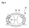
- FIG. 2 Another design option is the design with laminar conductive cores, as in FIG. 2 is shown.
- the figure shows a common mode push-pull reactor 100 having an outer core 102, an inner core 104 and a winding 106.
- the inner core 104 is closed by an air gap 108 and describes an eight.
- the outer core 102 forms or describes an oval.
- the winding 106 encloses both cores 102 and 104.
- FIG. 2 The arrangement and number of air gaps in FIG. 2 is selected by way of example and shows an arrangement with an air gap. Of course, other air gaps distributed over the magnetic path of the push-pull choke can be arranged.
- FIG. 3 shows a three-phase variant of a common-mode push-pull throttle, which is designated overall by the reference numeral 140.
- the illustration shows an outer core 142, an inner core 144, a first winding 146, a second winding 148, and a third winding 150.
- the presented common-mode push-pull choke is particularly suitable for use in single-phase and three-phase multi-string photovoltaic inverters.
- DC voltage is converted into alternating voltage and vice versa, and in which jumping potentials or a so-called CommonModeCurrent are to be prevented.
- FIG. 4 shows the potentials of an inverter 404, wherein the ground potential 403 is present as a possible reference potential on both the DC side and on the Konsdorfnseite.
- the potentials 402 of the conductors on the Kiruccinsei te can also be used as a reference potential in a Erdzug of the power grid.
- the potentials 401 of the DC side are usually capacitively coupled to the ground potential 403 and therefore may only have continuous values relative to the ground potential.
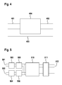
- FIG. 5 shows the basic arrangement of the common-mode and push-pull reactors of an inverter with multiple DC inputs.
- Reference numeral 501 denotes a first constant-value input with a first CMDM inductor 503 for smoothing and a first DC / DC adjuster 505 and reference numeral 502 a possible further constant-value input with a further CMDM inductor 504 and a further DC / DC adjuster 506 designated.
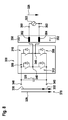
- FIG. 6 shows an embodiment of an inverter in an arrangement of the CMDM throttle 605 on the Kirdorfnseite 606.
- the DC / AC adjuster 604 converts the DC 601 into an alternating size.
- the inverter also includes a DC controller at the DC input, which consists of a DM reactor 602 and a Gleichehrnsteller 603.
- FIG. 7 shows the basic course of voltages in a single-phase inverter with H4 bridge and active freewheel, which also has a CMDM throttle. Based on the basic representation in FIG. 1 shows FIG. 7 in the first diagram 250 the course of a typical 230V mains voltage 40 at the terminals 42 and 44. The voltage curve at terminal 14 relative to the potential of the node 48 is sketched in the second diagram 252.
- the voltage curve is shown at terminal 16, again referred to the node 48. Both voltage waveforms are shown for a DC link voltage of 400V and also correspond to the switching states for the Switch 50 (negates for 56) for port 14 and 52 (and negates 54) for port 16.
- the voltage profile at the terminals 14 and 16 corresponds to averaged over a switching period of the output AC voltage (arrow 40) and is outlined in the sixth diagram 260. Based on the neutral or mains connection 44, the average voltage of terminals 14 and 16 corresponds to half the mains voltage (arrow 40).
- the mid-voltage jumps shown in the fourth graph 256 are received by the common mode choke with the coils 20 and 22 so that only a small magnetizing current builds up in the common mode choke, even when a freewheeling state is switched.
- the fifth graph 258 shows the voltage on a DM choke.
- the jumping of the potentials for example, at a photovoltaic generator can be prevented by the switching in the 20 kHz range or reduced to a fluctuation with the mains voltage. It thus remains the fluctuation with the mains voltage (50 Hz), as it can be seen in the absence of switching.
- FIG. 8 Figure 4 shows a standard H4 bridge 300 having a symmetrically distributed output inductor L1 302 and L2 304.
- the H4 bridge 300 includes a first switch S1 306, a second switch S2 308, a third switch S3 310, and a fourth switch S4 312. Further the illustration shows a capacitor C1 320 and a network 322.
- the mains voltage U Netz is indicated by an arrow 326.
- a further arrow 328 illustrates the voltage U a1 , an arrow 330 the voltage U ZK , an arrow 332 the voltage U a2 .
- a terminal a1 340, a terminal a2 342 and a terminal k1 344 and a terminal k2 346 is shown. Via the inductance L1 302, the voltage U L (arrow 350) drops as well as above the inductance L2 304 (arrow 352). Ports on network 322 are n1 360 and n2 362.
Landscapes
- Engineering & Computer Science (AREA)
- Power Engineering (AREA)
- Inverter Devices (AREA)
- Semiconductor Integrated Circuits (AREA)
Abstract
Es werden ein Wechselrichter (10) und ein Verfahren zum Wechselrichten vorgestellt. Bei dem Wechselrichter (10) ist eine Gleichtakt-Gegentakt-Drossel (18) vorgesehen, die in einem Bauteil integriert ist.An inverter (10) and a method of inverting are presented. In the inverter (10), a common-mode push-pull throttle (18) is provided, which is integrated in one component.
Description
Die Erfindung betrifft einen Wechselrichter, insbesondere einen Wechselrichter für eine Photovoltaikanlage, und ein Verfahren zum Wechselrichten einer Gleichgröße, insbesondere einer Gleichgröße, die von einem Photovoltaikmodul ausgegeben wird.The invention relates to an inverter, in particular an inverter for a photovoltaic system, and a method for inverting a DC variable, in particular a DC variable, which is output from a photovoltaic module.
Wechselrichter, die auch als Inverter bezeichnet werden, sind elektrische Geräte, die dazu dienen, eine Gleichspannung in eine Wechselspannung bzw. einen Gleichstrom in einen Wechselstrom umzurichten. Dabei können Wechselrichter für die Erzeugung von einphasigem oder mehrphasigem, üblicherweise dreiphasigem Wechselstrom ausgelegt sein.Inverters, also referred to as inverters, are electrical devices used to convert a DC voltage to an AC voltage or a DC to an AC current. Inverters can be designed for the generation of single-phase or multi-phase, usually three-phase alternating current.
Der hierin beschriebene Wechselrichter dient insbesondere für die elektrische Ener-giewandlung bei Photovoltaiksystemen, bei denen aus Gleichstrom Wechselstrom erzeugt werden soll.The inverter described herein is used in particular for the electrical energy conversion in photovoltaic systems, in which direct current alternating current is to be generated.
Aus der Druckschrift
Bei Wechselrichtern für Photovoltaikanlagen ist zu beachten, dass Potentialsprünge der Spannung an den Gleichstrom-Anschlüssen des Photovoltaikgenerators, bezogen auf Erde, zu unerwünschten kapazitiven Ableitströmen führen. Diese Spannungssprünge entstehen insbesondere durch Schaltfolgen der Leistungshalbleiter im Inverter. Abhängig von der zugrundeliegenden Schaltungstopologie können diese Spannungssprünge z. B. bei einem Wechsel von einem speisenden Zustand in einen Freilaufzustand oder umgekehrt auftreten.With inverters for photovoltaic systems, it should be noted that potential jumps refer to the voltage at the DC connections of the photovoltaic generator on earth, lead to unwanted capacitive leakage currents. These voltage jumps arise in particular due to switching sequences of the power semiconductors in the inverter. Depending on the underlying circuit topology, these voltage jumps z. B. occur when changing from a feeding state to a freewheeling state or vice versa.
Um die vorstehend erläuterten Potentialsprünge an den Gleichstrom-Anschlüssen des Photovoltaikinverters zu verhindern, sind eine Reihe von Maßnahmen bekannt:
- a) Verzicht auf das Schalten von Zuständen, die zu Spannungssprüngen führen, z.B. bei einer reinen H4-Brücke mit jeweils einer Induktivität in den Wechselspannungs-anschlüssen, Verzicht auf das Schalten von Freilaufzuständen.
- b) Bereitstellung eines Freilaufpfades, der vom Gleichstromanschluss für die Photovoltaikmodule entkoppelt ist, wie dies z.B. in den Druckschriften
DE10 2004 030 912 B3 EP 1 369 985 B1 - c) Galvanische Trennung durch Einsatz eines Transformators.
- d) Bezug eines Potentials der DC-Seite, insbesondere des Zwischenkreismittelpunkts, auf Erde. Dies ist bspw. in der Druckschrift
EP 1 861 914 B1 - e) Ein weiterer Vorschlag ist die Verwendung von Gleichtakt-Drosseln (CommonModeChoke, CMC) an den Anschlüssen des Photovoltaikgenerators, was in der Praxis derzeit jedoch nicht eingesetzt wird.
- a) waiver of the switching of states that lead to voltage jumps, eg in a pure H4 bridge, each with an inductance in the AC terminals, waiving the switching of freewheeling states.
- b) providing a freewheeling path which is decoupled from the DC connection for the photovoltaic modules, as for example in the publications
DE10 2004 030 912 B3 EP 1 369 985 B1 - c) Galvanic isolation by using a transformer.
- d) reference of a potential of the DC side, in particular of the DC link center, to ground. This is, for example, in the
publication EP 1 861 914 B1 - e) Another proposal is the use of common mode chokes (CommonModeChoke, CMC) at the PV array, which is not currently used in practice.
Die vorstehend beschriebenen Maßnahmen haben jedoch jeweils folgende Nachteile:
- a) Höhere Verluste bzw. geringerer Wirkungsgrad aufgrund größerer Stromrippel bei gleicher Schaltfrequenz.
- b) Zusätzlicher Bauteilaufwand insgesamt sowie ggf. erhöhte Durchlassverluste bei Einsatz zusätzlicher Leistungshalbleiter im speisenden Strompfad.
- c) Höhere Verluste durch den Transformator sowie zusätzlicher Materialaufwand und höheres Gewicht.
- d) Spezielle Modulationsverfahren (wie Flattop) zur Wirkungsgradsteigerung und/oder Absenkung der benötigten minimalen Zwischenkreisspannung sind nicht möglich, welche ein zum Neutralpunkt des Netzes verschiebbares Nullpunktsystem benötigen.
- e) Zusätzliche große Gleichtakt-Drossel notwendig (Gewicht, Kosten)
- a) Higher losses or lower efficiency due to larger current ripple at the same switching frequency.
- b) Additional component expenditure overall and possibly increased forward losses when using additional power semiconductors in the feeding current path.
- c) Higher transformer losses as well as additional material and weight.
- d) Special modulation methods (such as Flattop) for increasing the efficiency and / or lowering the required minimum intermediate circuit voltage are not possible, which require a neutral point of the network movable zero point system.
- e) Additional large common mode choke necessary (weight, cost)
Vor diesem Hintergrund werden ein Wechselrichter mit den Merkmalen des Anspruchs 1 und ein Verfahren zum Wechselrichten gemäß Anspruch 8 vorgestellt. Weitere Ausgestaltungen der Erfindung ergeben sich aus den abhängigen Patentansprüchen und der Beschreibung.Against this background, an inverter with the features of
Die Erfindung beschreibt eine Vorrichtung, die Potentialsprünge an den Gleichstrom-anschlüssen, wie diese vorstehend beschrieben sind, verhindert und dabei auf den Einsatz eines Transformators verzichtet. Die Unterdrückung der Potentialsprünge auf der Gleichgrößenseite bzw. DC-Seite wird dabei durch Einsatz einer Gleichtaktdrossel auf der Wechselgrößenseite bzw. AC-Seite sichergestellt. Die zusätzlich vorgesehene Gegentaktdrossel dient zum Bereitstellen eines sinusförmigen Signals.The invention describes a device which prevents potential jumps at the DC connections, as described above, and dispenses with the use of a transformer. The suppression of the potential jumps on the DC side or DC side is ensured by using a common mode choke on the AC side or AC side. The additionally provided push-pull throttle is used to provide a sinusoidal signal.
Des Weiteren kann die Gleichtakt-Gegentakt-Drossel und damit die Gleichtaktdrossel auf der Gleichgrößenseite angebracht sein, um dort die Potentialsprünge zu verhindern. Dies ist insbesondere dann sinnvoll, wenn auf der Gleichgrößenseite noch ein oder mehrere DC-Steller angebracht sind, die ihrerseits auch Potentialsprünge verursachen. In diesem Fall kann die entsprechende Gleichtaktdrossel zusätzlich zu den durch den Inverter verursachten Potentialsprüngen auf der AC-Seite auch die Potentialsprünge unterdrücken, die durch den entsprechenden DC-Steller erzeugt werden. Bei einem geeigneten Taktverfahren können die Potentialsprünge sich sogar gegenseitig zumindest teilweise aufheben.Furthermore, the common-mode push-pull throttle and thus the common mode choke can be mounted on the DC side to prevent the potential jumps there. This is particularly useful if on the Gleichgrößenseite one or more DC adjuster are attached, which in turn cause potential jumps. In this case, in addition to the potential jumps on the AC side caused by the inverter, the corresponding common mode choke can also suppress the potential jumps that are generated by the corresponding DC adjuster. In a suitable clocking process, the potential jumps can even cancel each other at least partially.
Die eingestellte Gleichtaktdrossel auf der AC-Seite arbeitet im Bereich der Taktfrequenz des Inverters bzw. der DC-Steller, üblicherweise in der Größenordnung 8 kHz bis 50 kHz, um den bei den Umschaltvorgängen der Halbleiter im Inverter oder im DC-Steller auftretenden Spannungssprung aufzunehmen. Aus EMV-Gründen eingesetzte Gleichtaktdrosseln sind hingegen derart ausgelegt, dass diese insbesondere in einem Bereich von > 150 kHz arbeiten und damit nicht gezielt die Grundfrequenz vorstehend beschriebener Potentialsprünge aufnehmen.The set common mode choke on the AC side operates in the range of the clock frequency of the inverter or the DC controller, usually in the order of 8 kHz up to 50 kHz to record the voltage jump occurring during the switching operations of the semiconductors in the inverter or in the DC controller. Common-mode chokes used for EMC reasons, on the other hand, are designed in such a way that they operate in particular in a range of> 150 kHz and thus do not specifically pick up the fundamental frequency of the above-described potential jumps.
Dabei wird in Ausgestaltung die gezielte Verbindung einer Schaltungseinrichtung mit einer kombinierten Gleichtakt-Gegentaktdrossel (CMDM-Drossel) auf der Wechselgrö-ßen- bzw. AC-Seite des Inverters eingesetzt. Dies ist sowohl im einphasigen Fall bei z.B. einer H4-Brücke möglich, wie auch im drei-/mehrphasigen Fall bei z.B. einem 3-phasigen Brückenzweig mit Freilauf oder NPC möglich. Damit können Sprünge der Spannungspotenziale an den Gleichstrom-Anschlüssen verhindert werden.In this case, in an embodiment, the targeted connection of a circuit device with a combined common mode differential mode choke (CMDM choke) on the Wechselgrö- ßen- or AC side of the inverter used. This is both in the single-phase case at e.g. H4 bridge possible, as well as in the three / multiphase case at e.g. a 3-phase bridge branch with freewheel or NPC possible. This prevents jumps in the voltage potentials at the DC connections.
In weiterer Ausgestaltung wird die gezielte Verbindung einer Inverterschaltung mit einer kombinierten Gleichtakt-Gegentaktdrossel auf der Gleichgrößen- bzw. DC-Seite des Inverters eingesetzt, insbesondere dann, wenn ein oder mehrere Gleichstrom-bzw. DC-Steller auf der Gleichgrößen-Seite der Gesamtschaltung vorgesehen werden, bei denen die Gleichstrom-Steller derart ausgeführt sind, dass Potentialsprünge auftreten. Dies ist insbesondere bei geteilten Gleichstrom-Stellern der Fall, die zeitversetzt betrieben werden, wodurch sich Wechselanteile in den Strömen gegenseitig aufheben können.In a further embodiment, the targeted connection of an inverter circuit is used with a combined common mode differential mode choke on the Gleichgrößen- or DC side of the inverter, especially if one or more DC or. DC controller are provided on the DC side of the overall circuit, in which the DC-adjuster are designed such that potential jumps occur. This is the case, in particular, in the case of split DC regulators, which are operated with a time delay, as a result of which alternating components in the currents can cancel each other out.
Der Vorteil gegenüber den vorstehend beschriebenen Maßnahmen gemäß dem Stand der Technik ist, dass gegenüber
- (a) nicht auf den Freilauf verzichtet werden muss,
- (b) auf zusätzliche Leistungshalbleiter-Bauteile verzichtet werden kann,
- (c) kein verlustbehafteter Transformator zusätzlich benötigt wird,
- (d) spezielle Modulationsverfahren zur Wirkungsgradsteigerung eingesetzt werden können,
- (e) durch die mögliche Kombination von Gleichtakt-Drosselfunktion und Gegentakt-Drosselfunktion bzw. Speicherdrosselfunktion in einer integrierten Drossel (CMDM-Drossel) der gesamte Drosselaufwand deutlich kleiner ausfällt, als bei der Variante mit einer CM-Drossel auf der PV-Generatorseite.
- (a) it is not necessary to forego freewheeling,
- (b) additional power semiconductor components can be dispensed with,
- (c) no lossy transformer is additionally required,
- (d) special modulation techniques can be used to increase efficiency,
- (e) by the possible combination of common mode throttle function and push-pull throttle function or storage throttle function in an integrated throttle (CMDM throttle), the total throttle effort is significantly smaller than in the variant with a CM throttle on the PV generator side.
Weiterhin ergeben sich durch die Doppelfunktion der Drossel EMV-Vorteile, da Gleich-taktstörungen durch die Gleichtaktdrosselfunktion ohne zusätzliche Bauelemente gefiltert werden können. Üblicherweise wird ansonsten bei einem Wechselrichter mit Frei-laufpfad eine separate CM-Drossel zur EMV-Filterung auf der Wechselgrößen-Seite benötigt.Furthermore, the double function of the throttle results in EMC advantages, since DC-clock interference can be filtered by the common-mode choke function without additional components. Usually, in the case of an inverter with a free-running path, a separate CM choke for EMC filtering on the alternating-current side is otherwise required.
Zu beachten ist, dass die eingesetzte Gleichtaktdrossel bzw. die Gleichtaktdrosselfunk-tion der CMDM-Drossel für einen Bereich der Taktfrequenz des Inverters ausgelegt ist, im Gegensatz zu einer Gleichtaktdrossel für EMV, deren Einsatzbereich üblicherweise erst > 150 kHz ist.It should be noted that the common mode choke or common mode choke function of the CMDM choke is designed for a range of clock frequency of the inverter, unlike a common mode choke for EMC, whose operating range is usually only> 150 kHz.
Der vorgestellte Wechselrichter ist nicht auf eine bestimmte Richtung des Leistungs-flusses festgelegt. Wird die Richtung des Leistungsflusses umgekehrt, so erzeugt der Wandler aus einer Wechselgröße eine Gleichgröße. Ein derartiger Einsatz ist bspw. beim Laden von Batterien für Elektrofahrzeuge vorgesehen.The presented inverter is not set to a specific direction of the power flow. If the direction of the power flow is reversed, the converter generates an equivalent quantity from an alternating quantity. Such an application is, for example, provided when charging batteries for electric vehicles.
Weitere Vorteile und Ausgestaltungen der Erfindung ergeben sich aus der Beschreibung und der beiliegenden Zeichnung.Further advantages and embodiments of the invention will become apparent from the description and the accompanying drawings.
Es versteht sich, dass die voranstehend genannten und die nachstehend noch zu erläuternden Merkmale nicht nur in der jeweils angegebenen Kombination, sondern auch in anderen Kombinationen oder in Alleinstellung verwendbar sind, ohne den Rahmen der vorliegenden Erfindung zu verlassen.It is understood that the features mentioned above and those yet to be explained below can be used not only in the particular combination indicated, but also in other combinations or in isolation, without departing from the scope of the present invention.
Kurze Beschreibung der Zeichnungen
Figur 1- zeigt in einer schematischen Darstellung eine Ausführungsform des beschriebenen Wechselrichters.
- Figur 2
- zeigt eine Ausführung einer Gleichtakt-Gegentakt-Drossel.
- Figur 3
- zeigt eine weitere Ausführung einer Gleichtakt-Gegentakt-Drossel.
- Figur 4
- zeigt einen Wechselrichter.
- Figur 5
- zeigt einen weiteren Wechselrichter.
- Figur 6
- zeigt noch einen weiteren Wechselrichter.
- Figur 7
- zeigt Signalverläufe.
- Figur 8
- zeigt eine Ausführung des Wechselrichters.
- FIG. 1
- shows a schematic representation of an embodiment of the described inverter.
- FIG. 2
- shows an embodiment of a common-mode push-pull throttle.
- FIG. 3
- shows a further embodiment of a common-mode push-pull throttle.
- FIG. 4
- shows an inverter.
- FIG. 5
- shows another inverter.
- FIG. 6
- shows another inverter.
- FIG. 7
- shows waveforms.
- FIG. 8
- shows an embodiment of the inverter.
Die Erfindung ist anhand von Ausführungsformen in den Zeichnungen schematisch dargestellt und wird nachfolgend unter Bezugnahme auf die Zeichnungen ausführlich beschrieben.The invention is schematically illustrated by means of embodiments in the drawings and will be described in detail below with reference to the drawings.
Der Aufbau einer Ausführungsform des beschriebenen Wechselrichters ist in einem Schaltbild in
Die Inverter/Brückenschaltung 12 umfasst einen ersten Schalter S1 50, einen zweiten Schalter S2 52, einen dritten Schalter S3 54 und einen vierten Schalter S4 56. Diese Schalter sind vorteilhafterweise als Halbleiterschalter, wie bspw. MOSFET, IGBT, mit interner oder zusätzlicher Freilaufdiode ausgeführt und durch das Ersatzschaltbild eines idealen Schalters mit Freilaufdiode dargestellt.The inverter /
Die Gleichtakt-Gegentaktdrossel 18 umfasst eine Gleichtaktdrossel 60 mit L1a 20 und L1 b 22 und eine Gegentaktdrossel 62 mit L1 c 24 und L1d 26.The common-mode
Bei einem beispielhaften Wechsel von Speisen nach Freilauf entsteht bei Verwendung einer reinen H4-Brücke (Inverter/Brückenschaltung 12) und der Gegentaktdrossel 62 ein Spannungssprung von UZK/2 an den Anschlussklemmen a1 46 und a2 48, da die Gegentaktdrossel in diesem Fall als induktiver Spannungsteiler arbeitet und daher die Spannung an den Anschlussklemmen bezogen zu einer Anschlussleitung des Netzes 42 oder 44 abhängig von der Schaltzustandsänderung der Schalter springt.In an exemplary change of food after freewheel arises when using a pure H4 bridge (inverter / bridge circuit 12) and the push-
Die Gleichtaktdrosselfunktion der Gleichtakt-Gegentaktdrossel 18 verhindert das Springen der Potentiale der Anschlussklemmen a1 46 und a2 48, da die Gleichtakt-drosselfunktion den Spannungssprung für eine gewisse Zeit aufnehmen kann. Dieser Spannungssprung, der an der Gleichtaktdrosselfunktion zu einem Spannungsabfall führt, muss durch ein geeignetes Ansteuerverfahren so gestaltet werden, dass der ge-mittelte Spannungsabfall über der Gleichtaktdrosselfunktion zu null wird. Ein dafür geeignetes Modulationsverfahren der Leistungsschalter wird nachstehend beschrieben.The common mode choke function of the common mode
Weiterhin ist zu beachten, dass die Größe der Gleichtaktdrosselfunktion von der Höhe des Spannungssprungs und von der Zeitdauer des Anliegens des Spannungsabfalls abhängig ist. Der dabei entstehende Magnetisierungsstrom muss durch geeignete Schaltungsmaßnahmen, wie bspw. Kondensatoren, abgeführt werden.It should also be noted that the magnitude of the common mode choke function depends on the magnitude of the voltage jump and on the duration of the voltage drop. The resulting magnetizing current must be removed by suitable circuit measures, such as, for example, capacitors.
Alternativ kann eine separate Ausführung der Gleichtakt-Gegentakt-Drossel als Gleich-taktdrossel (L1a, L1b)und Gegentaktdrossel (L1c, L1d) gewählt werden. Damit ergeben sich jedoch keine Einsparungen im Aufwand für die Drossel.Alternatively, a separate embodiment of the common-mode push-pull choke can be selected as DC-mode choke (L1a, L1b) and push-pull choke (L1c, L1d). However, this results in no savings in the effort for the throttle.
Nachfolgend werden zur Erläuterung Ausführungsformen von Gleichtakt-Gegentakt-Drosseln gegeben.Hereinafter, embodiments of common-mode differential chokes will be given for explanation.
Es ist zu berücksichtigen, dass die Herausforderung für den Bau einer Gleichtakt-Gegentakt-Drossel in der gemeinsamen Verwendung der Wicklung sowohl für die Gleichtakt- als auch für die Gegentaktfunktion der Drossel besteht. Dazu muss der Kern durch die Kupferwicklung sowohl die möglichst optimale, magnetische Kopplung zwischen beiden Drosseln für die Common Mode Filterung als auch über einen zweiten, über einen Luftspalt gehenden magnetischen Pfad die Differential Mode Filterung sicherstellen. Dies kann über einen umlaufenden Kern mit Mittelsteg mit Luftspalt ausgeführt werden. Dabei ist der Querschnitt A1 für die CM-Filterung zu dimensionieren sowie der Querschnitt A2 für die DM- Filterung auszulegen.It should be noted that the challenge for the construction of a common mode differential mode choke in the common use of the winding is for both the common mode and differential mode functions of the choke. For this purpose, the core must ensure through the copper winding both the best possible magnetic coupling between the two chokes for the common mode filtering as well as a second, over an air gap magnetic path differential mode filtering. This can be done via a rotating core with central web with air gap. In this case, the cross-section A1 for the CM filtering is to be dimensioned and the cross-section A2 interpreted for the DM filtering.
Eine weitere konstruktive Möglichkeit ist die Ausführung mit laminar leitenden Kernen, wie dies in
Die Anordnung und Anzahl der Luftspalte in
Es sind bei entsprechendem Ausgangsnetz oder Schaltungsausführung auch andere Ausführungen als zwei- oder dreiphasige Gleichtakt-Gegentakt-Drosseln denkbar. So kann bei einem dreiphasigen Wechselrichter mit einem weiteren Steller für den Neut-ralleiter dieser als vierte Phase betrachtet werden und eine vierphasige Gleichtakt-Gegentakt-Drossel zum Einsatz kommen.It is conceivable with appropriate output network or circuit design, other than two- or three-phase common mode differential mode chokes. Thus, in the case of a three-phase inverter with a further actuator for the neutral conductor, this can be regarded as the fourth phase and a four-phase common-mode push-pull throttle can be used.
Die vorgestellte Gleichtakt-Gegentakt-Drossel bietet sich insbesondere für den Einsatz in ein- und dreiphasigen Multistring-Photovoltaik-Wechselrichtern an. Es sind selbstverständlich auch andere Anwendungen denkbar, bei denen Gleichspannung in Wech-selspannung und umgekehrt gewandelt wird und bei der springende Potentiale bzw. ein sogenannter CommonModeCurrent verhindert werden soll.The presented common-mode push-pull choke is particularly suitable for use in single-phase and three-phase multi-string photovoltaic inverters. Of course, other applications are also conceivable in which DC voltage is converted into alternating voltage and vice versa, and in which jumping potentials or a so-called CommonModeCurrent are to be prevented.
Bei mehr als einem Gleichgrößeneingang mit einem DC/DC-Steller, der Gleichtakt-sprünge erzeugt, ist es zweckmäßig, die Filterdrosseln in einer CMDM-Ausführung an den Gleichgrößeneingängen zu installieren, die auch die Spannungssprünge des Inverters aufnehmen, da dann die Filterdrossel am Wechselgrößenanschluss des Wechselrichters nur für die Gegentaktstörungen ausgelegt werden muss.With more than one DC input with a DC / DC controller producing common mode hops, it is convenient to install the filter chokes in a CMDM version at the DC inputs, which also take the voltage jumps of the inverter, since then the filter choke at the AC terminal of the inverter must only be designed for differential mode interference.
Bei nur einem DC/DC-Steller ist es ein Optimierungsproblem, ob eine DM-Drossel am Gleichgrößeneingang und eine CMDM-Drossel am Wechselgrößeneingang oder eine CMDM-Drossel am Gleichgrößeneingang und eine DM-Drossel am Wechselgrößen-eingang zweckmäßig ist.With only one DC / DC controller, it is an optimization problem whether a DM choke at the DC input and a CMDM throttle at the AC input or a CMDM throttle at the DC input and a DM throttle at the AC input are useful.
Im dritten Diagramm 254 ist der Spannungsverlauf an Anschluss 16 dargestellt, wieder bezogen auf den Knoten 48. Beide Spannungsverläufe sind für eine Zwischenkreisspannung von 400V dargestellt und entsprechen auch den Schaltzuständen für die Schalter 50 (negiert für 56) für Anschluss 14 sowie 52 (und negiert 54) für Anschluss 16.In the third diagram 254, the voltage curve is shown at terminal 16, again referred to the
Der Spannungsverlauf an den Anschlüssen 14 und 16 entspricht gemittelt über eine Schaltperiodendauer der Ausgangswechselspannung (Pfeil 40) und ist im sechsten Diagramm 260 skizziert. Bezogen auf den Neutral- bzw. Netzanschluss 44 entspricht die gemittelte Spannung von Anschluss 14 und 16 der halben Netzspannung (Pfeil 40).The voltage profile at the terminals 14 and 16 corresponds to averaged over a switching period of the output AC voltage (arrow 40) and is outlined in the sixth diagram 260. Based on the neutral or
Die Sprünge der mittleren Spannung, die im vierten Diagramm 256 dargestellt sind, werden von der Gleichtaktdrossel mit den Spulen 20 und 22 aufgenommen, so dass sich nur ein kleiner Magnetisierungsstrom in der Gleichtaktdrossel aufbaut, auch wenn ein Freilaufzustand geschaltet wird. Im fünften Diagramm 258 ist die Spannung an einer DM-Drossel gezeigt.The mid-voltage jumps shown in the
Wie dargestellt ist, kann mit der Gleichtaktdrossel das Springen der Potentiale bspw. an einem Photovoltaik-Generator durch das Schalten im 20 kHz-Bereich verhindert bzw. zu einem Schwanken mit der Netzspannung vermindert werden. Es bleibt damit das Schwanken mit der Netzspannung (50 Hz), wie es bei dem Verzicht auf das Schalten auch zu sehen ist.As shown, with the common mode choke, the jumping of the potentials, for example, at a photovoltaic generator can be prevented by the switching in the 20 kHz range or reduced to a fluctuation with the mains voltage. It thus remains the fluctuation with the mains voltage (50 Hz), as it can be seen in the absence of switching.
Aufgrund der symmetrischen Verteilung (L1 = L2) ergeben sich für folgende Zustände die nachfolgenden Spannungsabfälle zwischen den Anschlussklemmen a1 340 und a2 342 und Erde 370. Es zeigt sich, dass bei einem Wechsel zwischen Speisen und Rückspeisen und einem Freilauf die Anschlusspotentiale um die halbe Zwischenkreisspannung UZK springen, nicht jedoch beim Schalten zwischen Speisen und Rückspeisen.Due to the symmetrical distribution (L1 = L2), the following voltage drops occur between the


Claims (9)
Applications Claiming Priority (1)
| Application Number | Priority Date | Filing Date | Title |
|---|---|---|---|
| DE201310211121 DE102013211121A1 (en) | 2013-06-14 | 2013-06-14 | inverter |
Publications (2)
| Publication Number | Publication Date |
|---|---|
| EP2814151A2 true EP2814151A2 (en) | 2014-12-17 |
| EP2814151A3 EP2814151A3 (en) | 2015-04-01 |
Family
ID=50819603
Family Applications (1)
| Application Number | Title | Priority Date | Filing Date |
|---|---|---|---|
| EP20140170024 Ceased EP2814151A3 (en) | 2013-06-14 | 2014-05-27 | Inverter |
Country Status (2)
| Country | Link |
|---|---|
| EP (1) | EP2814151A3 (en) |
| DE (1) | DE102013211121A1 (en) |
Cited By (5)
| Publication number | Priority date | Publication date | Assignee | Title |
|---|---|---|---|---|
| CN104660088A (en) * | 2015-03-04 | 2015-05-27 | 王曙光 | Variable-frequency inverter system for photovoltaic power generation |
| DE202016104544U1 (en) | 2016-08-18 | 2016-09-29 | Schneefuß + Rohde GmbH | Multi-phase push-pull power choke |
| DE102017222664A1 (en) | 2017-12-13 | 2019-06-13 | Robert Bosch Gmbh | Common-mode push-pull throttle for an electrically operable motor vehicle |
| DE102019122243A1 (en) * | 2019-08-19 | 2021-02-25 | Schmidbauer Transformatoren und Gerätebau GmbH | Power conversion system |
| WO2022033635A1 (en) * | 2020-08-12 | 2022-02-17 | innolectric AG | Resonance transformer having an additionally coupled inductor for an obc |
Citations (4)
| Publication number | Priority date | Publication date | Assignee | Title |
|---|---|---|---|---|
| DE102004030912B3 (en) | 2004-06-25 | 2006-01-19 | Sma Technologie Ag | Method for converting a direct electrical voltage of a DC voltage source, in particular a photovoltaic DC voltage source into an AC voltage |
| EP1861914B1 (en) | 2005-10-24 | 2008-12-03 | Conergy AG | Inverter |
| EP1369985B1 (en) | 2002-05-15 | 2009-05-13 | Fraunhofer-Gesellschaft zur Förderung der angewandten Forschung e.V. | Inverter for transforming a DC voltage into an AC current or an AC voltage |
| DE102009029387A1 (en) | 2009-09-11 | 2011-03-24 | Robert Bosch Gmbh | DC-AC inverter arrangement, in particular solar cell inverter |
Family Cites Families (2)
| Publication number | Priority date | Publication date | Assignee | Title |
|---|---|---|---|---|
| US6617814B1 (en) * | 2001-04-11 | 2003-09-09 | Rockwell Automation Technologies, Inc. | Integrated DC link choke and method for suppressing common-mode voltage in a motor drive |
| EP2672621B1 (en) * | 2012-06-07 | 2019-01-23 | ABB Research Ltd. | Method for zero-sequence damping and voltage balancing in a three-level converter with split dc-link capacitors and virtually grounded LCL filter |
-
2013
- 2013-06-14 DE DE201310211121 patent/DE102013211121A1/en not_active Withdrawn
-
2014
- 2014-05-27 EP EP20140170024 patent/EP2814151A3/en not_active Ceased
Patent Citations (4)
| Publication number | Priority date | Publication date | Assignee | Title |
|---|---|---|---|---|
| EP1369985B1 (en) | 2002-05-15 | 2009-05-13 | Fraunhofer-Gesellschaft zur Förderung der angewandten Forschung e.V. | Inverter for transforming a DC voltage into an AC current or an AC voltage |
| DE102004030912B3 (en) | 2004-06-25 | 2006-01-19 | Sma Technologie Ag | Method for converting a direct electrical voltage of a DC voltage source, in particular a photovoltaic DC voltage source into an AC voltage |
| EP1861914B1 (en) | 2005-10-24 | 2008-12-03 | Conergy AG | Inverter |
| DE102009029387A1 (en) | 2009-09-11 | 2011-03-24 | Robert Bosch Gmbh | DC-AC inverter arrangement, in particular solar cell inverter |
Cited By (7)
| Publication number | Priority date | Publication date | Assignee | Title |
|---|---|---|---|---|
| CN104660088A (en) * | 2015-03-04 | 2015-05-27 | 王曙光 | Variable-frequency inverter system for photovoltaic power generation |
| DE202016104544U1 (en) | 2016-08-18 | 2016-09-29 | Schneefuß + Rohde GmbH | Multi-phase push-pull power choke |
| WO2018033451A1 (en) | 2016-08-18 | 2018-02-22 | Manfred Schmelzer Gmbh | Multi-phase differential mode power choke |
| DE102017222664A1 (en) | 2017-12-13 | 2019-06-13 | Robert Bosch Gmbh | Common-mode push-pull throttle for an electrically operable motor vehicle |
| WO2019115207A1 (en) | 2017-12-13 | 2019-06-20 | Robert Bosch Gmbh | Common-mode/differential-mode throttle for an electrically driveable motor vehicle |
| DE102019122243A1 (en) * | 2019-08-19 | 2021-02-25 | Schmidbauer Transformatoren und Gerätebau GmbH | Power conversion system |
| WO2022033635A1 (en) * | 2020-08-12 | 2022-02-17 | innolectric AG | Resonance transformer having an additionally coupled inductor for an obc |
Also Published As
| Publication number | Publication date |
|---|---|
| DE102013211121A1 (en) | 2014-12-18 |
| EP2814151A3 (en) | 2015-04-01 |
Similar Documents
| Publication | Publication Date | Title |
|---|---|---|
| EP2737618B1 (en) | Electrical converter system | |
| EP2750920B1 (en) | Method and device for charging a battery of an electrical drive using components of the electrical drive | |
| EP2027647B1 (en) | Device for feeding electric energy into a power grid and dc converter for such a device | |
| EP1369985B1 (en) | Inverter for transforming a DC voltage into an AC current or an AC voltage | |
| EP2030299B1 (en) | Inverter for feeding electrical energy into a power supply system | |
| EP2815497B1 (en) | Grid feed apparatus, energy feed system and method for operating a grid feed apparatus | |
| AT505801B1 (en) | METHOD FOR OPERATING AN ELECTRONICALLY CONTROLLED INVERTER | |
| EP2863528B1 (en) | Operation of an inverter as a DC/DC-converter | |
| DE102007038959A1 (en) | inverter | |
| EP2623363B1 (en) | Apparatus and method for charging a traction battery of an electric vehicle | |
| EP2719051A2 (en) | Step-up converter | |
| EP2814151A2 (en) | Inverter | |
| DE102007038960A1 (en) | inverter | |
| EP2709257A2 (en) | Power converter circuit and method for controlling the power converter circuit | |
| EP2845303B1 (en) | Power converter and operating method for converting voltages | |
| EP2764614B1 (en) | Modular multilevel dc/ac converter comprising a series connection of dc/ac inverter sub-modules for the generation of polyphase output voltages | |
| WO2016066484A2 (en) | Inverter and reactor for rejecting common-mode interferences | |
| EP2421135B1 (en) | Transformerless inverter with step-down-converter | |
| EP2582030A2 (en) | Circuit arrangement with inverter | |
| DE102012220371A1 (en) | Device for charging high voltage battery of electric vehicle from three-phase alternating current voltage source, has switch switched by control device such that current and voltage of source are in phase with each other | |
| DE102020111355A1 (en) | Charging device and method for charging an electrical energy store of an electrically operated vehicle by means of a DC voltage converter which has different operating modes | |
| DE102008050765A1 (en) | Inverter arrangement for feeding photovoltaic energy into a public grid | |
| EP2221952A2 (en) | Bidirectional direct current adjuster and system | |
| DE102016224310A1 (en) | High efficiency power converter for single-phase systems | |
| DE102013212692A1 (en) | Energy storage device with DC power supply circuit |
Legal Events
| Date | Code | Title | Description |
|---|---|---|---|
| 17P | Request for examination filed |
Effective date: 20140527 |
|
| AK | Designated contracting states |
Kind code of ref document: A2 Designated state(s): AL AT BE BG CH CY CZ DE DK EE ES FI FR GB GR HR HU IE IS IT LI LT LU LV MC MK MT NL NO PL PT RO RS SE SI SK SM TR |
|
| AX | Request for extension of the european patent |
Extension state: BA ME |
|
| PUAI | Public reference made under article 153(3) epc to a published international application that has entered the european phase |
Free format text: ORIGINAL CODE: 0009012 |
|
| PUAL | Search report despatched |
Free format text: ORIGINAL CODE: 0009013 |
|
| AK | Designated contracting states |
Kind code of ref document: A3 Designated state(s): AL AT BE BG CH CY CZ DE DK EE ES FI FR GB GR HR HU IE IS IT LI LT LU LV MC MK MT NL NO PL PT RO RS SE SI SK SM TR |
|
| AX | Request for extension of the european patent |
Extension state: BA ME |
|
| RIC1 | Information provided on ipc code assigned before grant |
Ipc: H02M 1/00 20070101AFI20150226BHEP |
|
| R17P | Request for examination filed (corrected) |
Effective date: 20151001 |
|
| RBV | Designated contracting states (corrected) |
Designated state(s): AL AT BE BG CH CY CZ DE DK EE ES FI FR GB GR HR HU IE IS IT LI LT LU LV MC MK MT NL NO PL PT RO RS SE SI SK SM TR |
|
| RAP1 | Party data changed (applicant data changed or rights of an application transferred) |
Owner name: SMA SOLAR TECHNOLOGY AG |
|
| STAA | Information on the status of an ep patent application or granted ep patent |
Free format text: STATUS: EXAMINATION IS IN PROGRESS |
|
| 17Q | First examination report despatched |
Effective date: 20190423 |
|
| STAA | Information on the status of an ep patent application or granted ep patent |
Free format text: STATUS: EXAMINATION IS IN PROGRESS |
|
| STAA | Information on the status of an ep patent application or granted ep patent |
Free format text: STATUS: EXAMINATION IS IN PROGRESS |
|
| STAA | Information on the status of an ep patent application or granted ep patent |
Free format text: STATUS: THE APPLICATION HAS BEEN REFUSED |
|
| 18R | Application refused |
Effective date: 20230310 |