EP2291906B1 - Onduleur et procédé de fonctionnement de l'onduleur - Google Patents
Onduleur et procédé de fonctionnement de l'onduleur Download PDFInfo
- Publication number
- EP2291906B1 EP2291906B1 EP09769079.6A EP09769079A EP2291906B1 EP 2291906 B1 EP2291906 B1 EP 2291906B1 EP 09769079 A EP09769079 A EP 09769079A EP 2291906 B1 EP2291906 B1 EP 2291906B1
- Authority
- EP
- European Patent Office
- Prior art keywords
- freewheeling
- diode
- resonant
- semiconductor switch
- capacitor
- Prior art date
- Legal status (The legal status is an assumption and is not a legal conclusion. Google has not performed a legal analysis and makes no representation as to the accuracy of the status listed.)
- Not-in-force
Links
Images


Classifications
-
- H—ELECTRICITY
- H02—GENERATION; CONVERSION OR DISTRIBUTION OF ELECTRIC POWER
- H02M—APPARATUS FOR CONVERSION BETWEEN AC AND AC, BETWEEN AC AND DC, OR BETWEEN DC AND DC, AND FOR USE WITH MAINS OR SIMILAR POWER SUPPLY SYSTEMS; CONVERSION OF DC OR AC INPUT POWER INTO SURGE OUTPUT POWER; CONTROL OR REGULATION THEREOF
- H02M1/00—Details of apparatus for conversion
- H02M1/32—Means for protecting converters other than automatic disconnection
- H02M1/34—Snubber circuits
-
- H—ELECTRICITY
- H02—GENERATION; CONVERSION OR DISTRIBUTION OF ELECTRIC POWER
- H02M—APPARATUS FOR CONVERSION BETWEEN AC AND AC, BETWEEN AC AND DC, OR BETWEEN DC AND DC, AND FOR USE WITH MAINS OR SIMILAR POWER SUPPLY SYSTEMS; CONVERSION OF DC OR AC INPUT POWER INTO SURGE OUTPUT POWER; CONTROL OR REGULATION THEREOF
- H02M7/00—Conversion of ac power input into dc power output; Conversion of dc power input into ac power output
- H02M7/42—Conversion of dc power input into ac power output without possibility of reversal
- H02M7/44—Conversion of dc power input into ac power output without possibility of reversal by static converters
- H02M7/48—Conversion of dc power input into ac power output without possibility of reversal by static converters using discharge tubes with control electrode or semiconductor devices with control electrode
- H02M7/53—Conversion of dc power input into ac power output without possibility of reversal by static converters using discharge tubes with control electrode or semiconductor devices with control electrode using devices of a triode or transistor type requiring continuous application of a control signal
- H02M7/537—Conversion of dc power input into ac power output without possibility of reversal by static converters using discharge tubes with control electrode or semiconductor devices with control electrode using devices of a triode or transistor type requiring continuous application of a control signal using semiconductor devices only, e.g. single switched pulse inverters
- H02M7/5387—Conversion of dc power input into ac power output without possibility of reversal by static converters using discharge tubes with control electrode or semiconductor devices with control electrode using devices of a triode or transistor type requiring continuous application of a control signal using semiconductor devices only, e.g. single switched pulse inverters in a bridge configuration
-
- H—ELECTRICITY
- H02—GENERATION; CONVERSION OR DISTRIBUTION OF ELECTRIC POWER
- H02M—APPARATUS FOR CONVERSION BETWEEN AC AND AC, BETWEEN AC AND DC, OR BETWEEN DC AND DC, AND FOR USE WITH MAINS OR SIMILAR POWER SUPPLY SYSTEMS; CONVERSION OF DC OR AC INPUT POWER INTO SURGE OUTPUT POWER; CONTROL OR REGULATION THEREOF
- H02M1/00—Details of apparatus for conversion
- H02M1/32—Means for protecting converters other than automatic disconnection
- H02M1/34—Snubber circuits
- H02M1/346—Passive non-dissipative snubbers
-
- Y—GENERAL TAGGING OF NEW TECHNOLOGICAL DEVELOPMENTS; GENERAL TAGGING OF CROSS-SECTIONAL TECHNOLOGIES SPANNING OVER SEVERAL SECTIONS OF THE IPC; TECHNICAL SUBJECTS COVERED BY FORMER USPC CROSS-REFERENCE ART COLLECTIONS [XRACs] AND DIGESTS
- Y02—TECHNOLOGIES OR APPLICATIONS FOR MITIGATION OR ADAPTATION AGAINST CLIMATE CHANGE
- Y02B—CLIMATE CHANGE MITIGATION TECHNOLOGIES RELATED TO BUILDINGS, e.g. HOUSING, HOUSE APPLIANCES OR RELATED END-USER APPLICATIONS
- Y02B70/00—Technologies for an efficient end-user side electric power management and consumption
- Y02B70/10—Technologies improving the efficiency by using switched-mode power supplies [SMPS], i.e. efficient power electronics conversion e.g. power factor correction or reduction of losses in power supplies or efficient standby modes
Definitions
- the invention relates to an inverter for converting an input-side DC voltage into an output-side AC voltage comprising an H-bridge with four semiconductor switches, wherein at least one semiconductor switch clocks, wherein further between the H-bridge and output side AC voltage terminals, a storage inductor is provided and wherein the storage inductor a Freewheeling path with a freewheeling diode for commutation of the current after a shutdown of a semiconductor switch of the H-bridge comprises. Furthermore, the invention relates to a method for operating the inverter.
- inverter topologies are known.
- a very common feature is the so-called H-bridge.
- Four semiconductor switches, in particular IGBTs, are arranged in a bridge circuit.
- the triggering of the clocking semiconductor switch is usually carried out by means of pulse width modulation for simulating a sinusoidal voltage waveform of a connected AC voltage network, the clock frequency is a multiple of the mains frequency.
- Such an inverter topology is from the US-A-4937725 known.
- Inverters are increasingly being used to feed energy from alternative energy sources, such as solar generators or fuel cells, into public AC grids or island grids. To make this form of energy production economical, all components must have a high efficiency. This applies in particular to inverters for network-synchronous conversion of the energy obtained.
- Zero voltage switching (ZVS) and zero current switching (ZCS) are known.
- Another source of power losses represent the freewheeling phases after switching off a semiconductor switch. These arise through the output side arranged inductor circuits whose inductor current continues to flow when the semiconductor switch is turned off. Freewheeling paths within an inverter circuit are usually via parasitic diodes of the semiconductor switches or via dedicated freewheeling diodes. Since a voltage is applied to these diodes usually at the beginning of a freewheeling phase, arise during the rise of the current through the diodes, a power loss that limits the efficiency of the inverter to the top.
- the invention has the object of developing the known from the prior art inverter to achieve improved efficiency.
- each clocking semiconductor switch is coupled to the zero voltage switching to a resonant circuit comprising capacitive resonant elements and inductive resonant elements
- the freewheeling path comprises a first and a second freewheeling diode in parallel
- said parallel circuit in Series is connected to the inductive resonant elements
- the second freewheeling diode is connected in series with capacitive freewheeling elements which as elements of the resonant circuit at the beginning of a freewheeling phase for zero voltage switching of the second freewheeling diode to a corresponding voltage charged.
- the energy stored in the resonant circuit during a turn-off phase is used to charge the capacitive freewheeling elements in a switch-on phase of the clocking semiconductor switch.
- the freewheeling elements are connected in series with the second freewheeling diode in order to de-energize them at the beginning of a freewheeling phase.
- the capacitive freewheeling elements discharge in a first period of the freewheel, wherein the first freewheeling diode is de-energized and commutes the freewheeling current without losses to the first freewheeling diode.
- the circuit according to claim 1 thus enables on the one hand a lossless switching of the semiconductor switch of the H-bridge and on the other hand a nearly lossless freewheel after switching off the clocking semiconductor switch.
- each resonant circuit comprises a resonant capacitor and a resonant choke, wherein a freewheeling capacitor is connected via coupling elements with a resonant capacitor and wherein a first branch of the freewheeling path comprises the first freewheeling diode and the resonant choke connected in series and wherein a second branch of the freewheeling path second freewheeling diode, the resonance choke and the freewheeling capacitor in series circuit comprises.
- the coupling elements are formed, for example, by diode circuits for determining a corresponding current direction during a resonant oscillation or by transformers. Over the coupling elements energy is thus transferred from the resonant capacitor to the freewheeling capacitor after a turn-on of the clocking semiconductor switch to ensure a power-free freewheel for the next shutdown.
- the freewheeling path comprises a further H-bridge with four auxiliary semiconductor switches, the first auxiliary semiconductor switch of the further H-bridge being connected via the first storage inductor and the third auxiliary semiconductor switch of the further H-bridge being connected via the second storage inductor to the first AC voltage terminal and the second Auxiliary semiconductor switch of the further H-bridge via the third storage inductor and the fourth auxiliary semiconductor switch of the further H-bridge via the fourth storage inductor are connected to the second AC voltage terminal.
- Such a connection of the H-bridge and the further H-bridge via four storage chokes to the two AC voltage connections has the advantage that both during a positive and during a negative half cycle of the AC voltage, a freewheeling path is available without the use of the parasitic diodes in the auxiliary semiconductor switches , This avoids losses that would otherwise be caused during a freewheeling by the usually slow parasitic diodes.
- connection of the third and the fourth auxiliary semiconductor switch and the connection of the first and the second auxiliary semiconductor switch via a series circuit of the first freewheeling diode and a resonance choke are connected in parallel to the first free-wheeling diode series connection is arranged from the second freewheeling diode and freewheeling capacitor, that further comprises a connection point between the second freewheeling diode and freewheeling capacitor via a Series circuit of a third diode and a fourth diode is connected to the connection of the first and the second auxiliary semiconductor switch, that in parallel to the third diode, a secondary winding of a transformer is arranged, which also comprises two primary windings, wherein the first primary winding with one end to the compound of is connected to the other end via a first resonant capacitor to the connection between the first semiconductor switch and the first storage inductor and a second resonant capacitor to the connection between the second semiconductor switch and the third storage inductor and wherein the second
- one half of the H-bridge is connected via a first storage inductor to a first AC voltage terminal and the other half of the H-bridge is connected to a second AC voltage terminal via a second storage inductor.
- the freewheeling path comprises a further H-bridge with four auxiliary semiconductor switches, wherein one half of the further H-bridge is connected to the first AC voltage connection via the first storage inductor and the other half of the further H-bridge is connected via the second storage inductor to the second VLC voltage connection is switched.
- Such a circuit with only two storage chokes at the inverter outputs is useful when the auxiliary semiconductor switches have fast parasitic diodes, whereby the losses during the freewheel small being held.
- the first and fourth semiconductor switches clock during a positive half cycle, and the second and third semiconductor switches during a negative half cycle.
- a circuit supplement is advantageous in which the connection of the third and the fourth auxiliary semiconductor switch and the connection of the first and the second auxiliary semiconductor switch via a series circuit of a second resonance choke, the first free-wheeling diode and a first Resonance choke are connected, and in parallel to the first freewheeling diode, a series circuit of a second freewheeling capacitor, the second freewheeling diode and a first freewheeling capacitor is arranged.
- connection point between the second freewheeling diode and the first freewheeling capacitor via a series circuit of a third diode and a fourth diode connected to the connection of the first and second auxiliary semiconductor switch and the connection of the third and the fourth auxiliary semiconductor switch via a sixth diode and a fifth diode with a connection point between the second freewheeling diode and the second freewheeling capacitor connected.
- a connection point between third and fourth diode via a first resonant capacitor to the connection of the first semiconductor switch and the second semiconductor switch and a connection point between the fifth and sixth diode via a second resonant capacitor connected to the compound of the third semiconductor switch and the fourth semiconductor switch.
- simple diode circuits are arranged as coupling elements between the resonance capacitors, the resonance chokes and the freewheeling capacitors.
- the Current flows between these devices flow during a clock cycle in such a way that the diodes in these diode circuits as well as the free-wheeling diodes become conductive without loss.
- One clock cycle is determined by a switch-on of a clocking semiconductor switch to the next power-on.
- the first resonant circuit which comprises the first resonant capacitor, the first freewheeling capacitor and the first resonant choke
- the second resonant circuit which comprises the second resonant capacitor, the second freewheeling capacitor and the second resonant choke, serves for the zero voltage switching of the third and the fourth semiconductor switch.
- the resonance capacitors are charged to almost half the input side DC voltage before a switch-on.
- a further embodiment of the invention provides that a first H-bridge connection between the first semiconductor switch and the fourth semiconductor switch is connected via a first storage choke to a first AC voltage terminal and a second H-bridge connection between the second semiconductor switch and the third semiconductor switch via a second storage choke with a second Furthermore, the connection of the third and the fourth semiconductor switch via a series circuit of the first freewheeling diode and the first resonant choke are connected to the first H-bridge connection that parallel to the first freewheeling diode a series circuit of the second freewheeling diode and the first freewheeling capacitor is arranged, that parallel to the first semiconductor switch, a series circuit of a first reson capacitor and a fourth diode is arranged and that a connection point between the second Freewheeling diode and first freewheeling capacitor is connected via a third diode to a connection point between the first resonant capacitor and the fourth diode, further that the connection of the third and the fourth semiconductor switch via a series circuit of another first freewheeling diode and second
- This embodiment is thus designed as an inverter with mains transformer.
- only one semiconductor switch clocks namely only the first semiconductor switch during a positive half-cycle; the third semiconductor switch is always on and the second and fourth semiconductor switches are always off.
- the second semiconductor switch clocks and the fourth semiconductor switch is always on; the first and third semiconductor switches are always off.
- the DC voltage connections are connected to one another via an input capacitor. This is especially appropriate if the input side in the Power fluctuating power source is connected, such as a solar generator.
- the AC voltage connections are connected to one another via an output capacitor.
- a method for operating one of the inverters described above provides that at the beginning of a clock cycle at least one semiconductor switch of the H-bridge is turned on, that while the input-side DC voltage is drawn to the inductive resonant elements of the respective resonant circuit, whereby the still as a freewheeling current through the inductive Resonance elements flowing current decreases and reverses its direction and that subsequently by means of this current energy is transferred from the capacitive resonance elements to the capacitive freewheeling elements, that after a predetermined switch-on the at least one clocking semiconductor switch is switched off again and at least a portion of the freewheeling current through the second freewheeling diode, the capacitive freewheeling elements and the inductive resonance elements flows until the capacitive freewheeling elements are discharged and the remaining freewheeling current through the first freewheeling diode and the inductive Reso nanzetti flows.
- This is a passive, low-loss method for reducing the switching losses of semiconductors, in particular IGBTs, specified as an H-
- a first embodiment of the invention is in Fig. 1 shown.
- the H-bridge is equipped with four semiconductor switches S1, S2, S3, S4 Input side to an energy source 1, for example, a power source, a voltage source or a non-linear source (solar generator) connected.
- An input capacitor Cin buffers the energy in a given voltage range.
- the first semiconductor switch S1 is connected via a first storage inductor L1 and the third semiconductor switch S3 is connected via a second storage inductor L2 to a first AC voltage connection.
- the second semiconductor switch S2 is connected via a third storage inductor L3 and the fourth semiconductor switch S4 is connected via a fourth storage inductor L4 to a second AC voltage connection.
- a consumer network 2 is connected to the two inverter connections. In this case, an output capacitor Co ensures a smoothing of the current fed into the consumer network 2.
- a further H-bridge with four auxiliary semiconductor switches HS1, HS2, HS3, HS4 is arranged.
- These auxiliary semiconductor switches HS1, HS2, HS3, HS4 are connected in parallel to the semiconductor switches S1, S2, S3, S4 of the first H-bridge to the four storage inductors L1, L2, L3, L4.
- the counting of the semiconductor switches S1, S2, S3, S4 and the auxiliary semiconductor switches HS1, HS2, HS3, HS4 takes place in the usual manner for an H-bridge representation in a clockwise direction.
- the semiconductor switches S1, S2, S3, S4 and Hilfshalbeiterschalter HS1, HS2, HS3, HS4 are formed for example as IGBTs. In Fig. 1 they are shown as such, each with a parasitic diode (body diode).
- a double resonance circuit is arranged.
- one side of a first resonance choke RL1 is connected to the cathode of a fourth diode D4.
- the anode of this fourth diode D4 is connected via a first resonant capacitor RC1 to the Bridge connection of the first and second semiconductor switches S1, S2 connected.
- this one side of the first resonance choke RL1 is connected to the bridge connection of the first and the second auxiliary semiconductor switch HS1, HS2.
- the other side of the first resonant choke RL1 is connected to the cathode of a first freewheeling diode D1 and also connected via a first freewheeling capacitor FC1 on the one hand to the cathode of a second freewheeling diode D2 and on the other hand via a third diode D3 to a connection point between the first resonant capacitor RC1 and fourth diode D4 ,
- the third diode D3 is switched from the first freewheeling capacitor FC1 to the first resonance capacitor RC1 in the forward direction.
- a second resonant capacitor RL2 is connected via a sixth diode D6 and a second resonant capacitor RC2 to the bridge connection between third and fourth semiconductor switches S3, S4.
- the sixth diode D6 is arranged from the second resonant choke RL2 to the second resonant capacitor RC2 in the forward direction.
- This one side of the second resonant choke RL2 is also connected to the bridge connection between the third and fourth auxiliary semiconductor switches HS3, HS4.
- the other side of the second resonant choke RL2 is connected on the one hand to the anode of the first filament diode D1 and on the other hand via a second freewheeling capacitor FC2 to the anode of the second freewheeling diode D2.
- a fifth diode D5 is arranged in the forward direction from the second resonance capacitor RC2 to the second free-running capacitor FC2.
- the main circuit consists of an H-bridge whose semiconductor switches S1, S2, S3, S4 are switched by means of a controller with a predetermined clock frequency.
- the auxiliary switching elements HS1, HS2, HS3, HS4 are switched on and off by means of control with a predetermined mains frequency (for example 50 Hz).
- the clock frequency exceeds the mains frequency by a multiple.
- the circuit allows the freewheeling current of the storage chokes L1, L2, L3, L4, after turning off the semiconductor switches S1, S4 during a positive half-wave and S2, S3 during a negative half cycle, only as rectifier diode D1 and not by the slower switching parasitic diodes the auxiliary semiconductor switch HS1, HS2, HS3, HS4 to flow.
- FIGS. 3 and 4 the switching phases are shown during a positive half cycle of the output alternating current.
- the first and fourth semiconductor switches S1, S4 are switched at the clock frequency, the second and third semiconductor switches S2, S3 remain off.
- the first and the fourth auxiliary semiconductor switches HS1, HS4 are always switched on during a positive half-cycle, the two other auxiliary semiconductor switches HS2, HS3 are either switched off or clocked inverting to the clocking semiconductor switches S1, S4 of the first H-bridge.
- the first and fourth semiconductor switches S1, S4 are turned on.
- the current flows from the power source 1 coming through the first semiconductor switch S1, the first storage inductor L1, a connected network 2 and further via the fourth storage inductor L4 and the fourth semiconductor switch S4 back to the power source.
- the first and fourth semiconductor switches S1, S4 are turned off.
- the freewheeling current of the first and the fourth storage inductor L1, L4 flows through the free-wheeling diode D1, the first and the fourth auxiliary semiconductor switches HS1, HS4 and via the network 2.
- Analog to the switching phases during a positive half cycle are in the FIGS. 5 and 6 the switching phases during a negative half wave are shown.
- the first and the fourth semiconductor switches S1, S4 are always switched off during a negative half-cycle.
- the second and third semiconductor switches S2, S3 clock at the clock frequency.
- the first and fourth auxiliary semiconductor switches HS1, HS4 are either switched off or clocked in inverting to the clocking semiconductor switches S2, S3 of the first H-bridge.
- the other two auxiliary semiconductor switches HS2, HS3 are always switched on during a negative half-wave.
- a switch-on phase flows from the power source 1 coming through the second semiconductor switch S2, the third storage inductor L3, the connected network 2 and the second storage inductor L2 and the third semiconductor switch S3 back to the power source.
- the second and third semiconductor switches S2, S3 are turned off.
- the freewheeling current of the second and third storage inductor L2, L3 flows through the freewheeling diode D1 and also through the second and third auxiliary semiconductor switches HS2, HS3 and via the network 2.
- one clock cycle (a sequence of a switch-on phase and a switch-off phase) is subdivided into a plurality of time sections.
- FIGS. 7 to 11 is the embodiment described above with resonant circuits ( Fig. 1 ), wherein the current flows occurring in individual periods are plotted during a positive half cycle.
- the corresponding current and voltage curves over time are in the FIGS. 12 to 14 shown.
- One clock cycle begins at the turn-on time t0 with the on-switch of the first and fourth semiconductor switches S1, S4. It is assumed that, shortly before switching on, the freewheeling current of the first and fourth storage inductors L1, L4 flows through the first freewheeling diode D1 via the first and fourth auxiliary semiconductor switches HS1, HS4 and the first and second resonance inductors RL1, RL2. Furthermore, the first resonant capacitor RC1 is charged to almost half the voltage of the input capacitor Cin (or half the voltage of a solar generator connected, for example, on the input side), the negative potential of the first resonant capacitor RC1 being at the anode of the fourth diode D4.
- the second resonant capacitor RC2 is also charged to half the voltage of the input capacitor Cin (or half the voltage of a solar generator, for example, on the input side), its positive potential being at the cathode of the sixth diode D6 ( Fig. 7 ).
- a first time interval t0-t1 is in Fig. 8 shown.
- the first and fourth semiconductor switches S1, S4 are turned on.
- the current from the input-side power source 1 flows through the first and fourth semiconductor switches S1, S4 through the first and fourth storage inductors L1, L4.
- With the power switch of the first Semiconductor switch S1 is also a first resonant circuit, consisting of the first resonant capacitor RC1, the first resonant choke RL1 and the first freewheeling capacitor FC1 activated.
- a second resonant circuit consisting of the second resonant capacitor RC2, the second resonant choke RL2 and the second freewheeling capacitor FC2, which is activated by turning on the fourth semiconductor switch S4.
- the potential at the emitter of the first auxiliary semiconductor switch HS1 goes up massively, while the first resonance choke RL1 reduces its stored energy by driving its current into a very high voltage (the two resonance chokes RL1, RL2 are to a certain extent at the input side voltage). After a very short time, these two inductors RL1, RL2 have built up their magnetic field. As a result, the free-wheeling current in the first freewheeling diode D1 approaches zero via the two resonance chokes RL1, RL2.
- FIG. 12 shows the uppermost diagram shows the gate-source voltage S1-U GD at the first semiconductor switch S1.
- Fig. 12 below the course of the drain current S1-I D and the drain voltage S1-U D of the first semiconductor switch S1 is shown in a diagram. It follows from top to bottom a diagram with the current RC1-I and the voltage RC1-U of the first resonant capacitor RC1 over time, a graph with the current FC1-I and the voltage FC1-U of the first free-wheeling capacitor FC1 over time and a diagram with the current RL1-I and the voltage RL1-U of the first resonant choke RL1 over time.
- Fig. 13 shows from top to bottom the current D1-I and the voltage D1-U of the first freewheeling diode D1, the current D2-I and the voltage D2-U of the second freewheeling diode D2, the current D3-I and the voltage D3-U of the third Diode D3 and the current D4-I and the voltage D4-U of the fourth diode D4.
- Fig. 14 is finally from top to bottom a diagram with the current S1-I through the first semiconductor switch S1 and with the input current I in over time, a diagram with the current L1-I in the first storage inductor L1 (output current) and the current HS1- I through the first auxiliary semiconductor switch HS1 over time, a diagram with the current BDHS1-I through the parasitic diode of the first auxiliary semiconductor switch HS1 and the current HS1-I through the first auxiliary semiconductor switch HS1 over time and a diagram with the current BDSH2-I through the parasitic diode of the second auxiliary semiconductor switch HS2 and with the current L1-I in the first storage inductor L1 over time.
- the charge of the first resonant capacitor RC1 oscillates with a half cycle of the resonant frequency to the first free-wheel capacitor FC1. This is done by a current flow through the first semiconductor switch S1, the parasitic diode of the first auxiliary semiconductor switch HS1, the first resonant choke RL1 and the third diode D3.
- the charge of the second resonant capacitor RC2 oscillates with a half cycle of the resonant frequency to the second freewheeling capacitor FC2, wherein in this case the current through the fourth semiconductor switch S4, the fifth diode D5, the second resonant inductor RL2 and the parasitic diode of the fourth auxiliary semiconductor switch HS4 flows.
- the first freewheeling diode D1 switches off with zero voltage and the third and the fifth diode D3, D5 are turned on with zero voltage. Accordingly, no power loss is lost at these diodes.
- the charges of the resonance capacitors RC1, RC2 are completely transferred to the freewheeling capacitors FC1, FC2.
- the third diode D3 as well as the fifth diode D5 switches off with zero current and prevents further oscillation in the resonant circuits RC1, FC1, RL1 or RC2, FC2, RL2.
- the current from the power source 1 continues to flow in the first and fourth storage inductors L1, L4 via the first and fourth semiconductor switches S1, S4.
- the first and fourth semiconductor switches S1, S4 are turned off by means of a corresponding control (eg according to the pulse width modulation method).
- the current from the energy source 1 continues to flow via a parallel branch, namely, via the resonance capacitors RC1, RC2, via the fourth and sixth diodes D4, D6 and via the first and fourth auxiliary semiconductor switches HS1, HS4.
- the resonant capacitors RC1, RC2 are charged very quickly by the current in the storage chokes L1, L4.
- the freewheeling capacitors FC1, FC2 release their charge via the second free-wheeling diode D2, the resonance chokes RL1, RL2, the first and the fourth auxiliary semiconductor switches HS1, HS4 and the storage chokes L1, L4 to the connected network 2.
- the freewheeling capacitors FC1, FC2 are completely discharged.
- t4-t5 takes over again the first freewheeling diode D1, the freewheeling current.
- the same description sequence applies to the second and third semiconductor switches S2, S3 as clocking switches and to the second and third auxiliary semiconductor switch HS2, HS3 as an activated switch of the freewheel.
- the current flows through the second and the third storage inductor L2, L3.
- a resonance circuit with a transformer T is provided as a coupling element.
- a resonant choke RL is first connected in series with the first freewheeling diode D1.
- Parallel to the first freewheeling diode D1, the second freewheeling diode D2 is arranged in series with a freewheeling capacitor FC.
- a connection point between the second freewheeling diode D2 and freewheeling capacitor is connected via a third and a fourth diode D3, D4 to the bridge connection between the first and second auxiliary semiconductor switches HS1, HS2.
- a secondary winding of the transformer T is arranged parallel to the third diode, wherein the winding start of the secondary winding to the cathode of the third diode D3 and the anode of the fourth diode D4 is connected.
- the winding end is connected to the cathode of the second freewheeling diode D2 and one side of the freewheeling capacitor FC.
- the first primary winding is connected to the winding start on the one hand via a first resonant capacitor RC1 with a connection between the first semiconductor switch S1 and first storage inductor L1 and the other via a second resonant capacitor RC2 with a connection between the second semiconductor switch S2 and third storage inductor L3.
- the winding end of the first primary winding is connected to the bridge connection between the first and second semiconductor switches S1, S2.
- the winding start of the second primary winding to the bridge connection between the third and fourth semiconductor switch 53, S4 and the winding end of the second primary winding is connected on the one hand via a third resonant capacitor RC3 with a connection between the third semiconductor switch S3 and second storage inductor L2 and the other via a fourth resonant capacitor RC4 with a connection between the fourth semiconductor switch S4 and fourth storage inductor L4.
- FIGS. 16 to 20 show the current flows during a clock cycle in the previously defined periods t0-t1, t1-t2, t2-t3, t3-t4 and t4-t5 during a positive half cycle.
- the freewheeling current of the first and fourth storage inductors L1, L4 flows through the network, through the first and fourth auxiliary semiconductor switches, the first freewheeling diode D1 and the resonance inductor RL (FIG. Fig. 16 ).
- the charges of the second and the fourth resonant capacitor RC1, RC4 are transposed over the transformer T, the resonant choke RL and the fourth diode D4 onto the freewheeling capacitor FC ( Fig. 18 ).
- the fourth time interval t3-t4 introduced in this way is in Fig. 20 shown.
- current continues to flow from the energy source 1 via the first and the fourth resonance capacitor RC1, RC4 and the transformer T, which is in a flow phase, since the secondary diode D3 arranged on the secondary side is conductive. This happens until the two resonance capacitors RC1, RC4 are charged.
- the freewheeling capacitor FC discharges its charge to the network 2 via the second free-wheeling diode D2, the resonance choke RL and the first and the second auxiliary semiconductor switches HS1, HS4.
- the two resonance capacitors RC1, RC4 are fully charged and the current from the power source 1 goes to zero.
- the freewheeling capacitor FC is completely discharged and the freewheeling current commutates at zero voltage from the second freewheeling diode D2 to the first freewheeling diode D1.
- the illustrated embodiments of the invention have the advantage that all involved switching components (semiconductor switches and diodes) either at zero voltage or at zero current on or off. In this way, the switching losses of the inverter are reduced to a minimum.
- the concept can be simplified by arranging only two storage inductors L1, L2 instead of the four storage inductors L1-L4 described so far at the output of the inverter are.
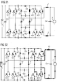
- the corresponding circuit is in Fig. 21 shown.
- Fig. 1 Opposite the circuit in Fig. 1 is here in the H-bridge of the first and fourth semiconductor switches S1, S4 connected to each other. Likewise, the second and third semiconductor switches S2, S3 are connected together. These connections are connected via a respective storage inductor L1, L2 to the AC voltage outputs. Parallel to this, the further H-bridge for the freewheel is arranged, wherein also here the first and the fourth auxiliary semiconductor switch HS1, HS4 and the second and the third auxiliary semiconductor switch HS2, HS3 are interconnected.
- the general switching conditions of such a circuit are as follows. During a positive half-cycle, the first and third semiconductor switches S1, S3 clock at the clock frequency, while the second and fourth semiconductor switches S2, S4 remain permanently switched off.
- the first and third auxiliary semiconductor switches HS1, HS3 are always turned on during a positive half-cycle, whereas the second and fourth auxiliary semiconductor switches HS2, HS4 are either turned off or clocked inversely to the semiconductor switches S1, S3.
- the second and fourth semiconductor switches S2, S4 and the first and third semiconductor switches S1, S3 remain switched off.
- the first and third auxiliary semiconductor switches HS1, HS3 are either switched off or clocked inverting the semiconductor switches S1, S3.
- the second and fourth auxiliary semiconductor switches HS2, HS4 are always turned on during a negative half cycle.
- HS4 is divided ( Fig. 22 . Fig. 27-29 ).
- the first resonant capacitor RC1 is charged with the half-cycle of the resonant frequency via the first semiconductor switch S1, the parasitic diode of the first auxiliary semiconductor switch HS1, the first resonant reactor RL1, and the third diode D3 first freewheeling capacitor FC1.
- the recharging of the second resonant capacitor RC2 to the second freewheeling capacitor FC2 via the fifth diode D5, the second resonant inductor RL2, the parasitic diode of the third auxiliary semiconductor switch HS3 and the third semiconductor switch S3 ( Fig. 24 . Fig. 27-29 ).
- the beginning of the fourth time interval t3-t4 is marked by the switching off of the first and third semiconductor switches S1, S3.
- the current from the power source 1 continues to flow through the resonance capacitors RC1 and RC2, via the fourth diode D4 and the sixth diode D6 and the first auxiliary semiconductor switch HS1 and the third auxiliary semiconductor switch HS3, respectively, until the two resonance capacitors RC1, RC2 are charged.
- the disconnecting capacitors FC1, FC2 give their charge via the second freewheeling diode D2, the first and third auxiliary semiconductor switches HS1, HS3 and the resonance chokes RL1, RL2 and the coil chokes L1, L2 to the network until they are completely discharged ( Fig. 26 . Fig. 27-29 )
- the resonance capacitors are fully charged and the current from the energy source 1 goes to zero.
- the freewheeling capacitors are completely discharged and the freewheeling current commutates at zero voltage from the second freewheeling diode D2 to the first freewheeling diode D1 and the parallel-connected parasitic or antiparallel diodes of the second and the fourth auxiliary semiconductor switch HS2, HS4.
- the freewheeling current flows divided into the first freewheeling diode D1 and the parallel-connected parasitic or antiparallel diodes of the second and fourth auxiliary semiconductor switches HS2, HS4 until the next switching-on process takes place ( Fig. 22 . Fig. 27-29 ).
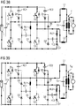
- Another embodiment of the present invention relates to an inverter with a mains transformer for galvanic isolation of the input side connected energy source 1 and the output side connected AC voltage network. 2
- An H-bridge with four semiconductor switches S1, S2, S3, S4 is as known on the input side to the power source 1 and the output side via two storage inductors L1, L2 connected to a primary winding of a power transformer T N. If necessary, an input capacitor Cin and, parallel to the primary winding, an output capacitor Co are on the input side arranged. Via a secondary winding of the power transformer T N , the connection to the network 2 ( Fig. 30 ).
- the clocking at the clock frequency semiconductor switches are switched unbalanced.
- the second and fourth semiconductor switches S2, S4 are always switched off, the third semiconductor switch S3 is always switched on and the first semiconductor switch S1 is clocked.
- the freewheeling current flows through the antiparallel or parasitic diode of the fourth semiconductor switch S4 and the switched-third semiconductor switch S3.
- the second semiconductor switch S2 clocks, the fourth semiconductor switch S4 always remains switched on and the first and third semiconductor switches S1, S3 always remain switched off.
- the freewheeling current flows here via the antiparallel or parasitic diode of the third semiconductor switch S3 and via the switched fourth semiconductor switch S4.
- the permanently switched semiconductor switches S3 and S4 and the clocking semiconductor switches S1 and S2 are reversed to be controlled. Accordingly, during a positive half cycle, the third semiconductor switch S3 can also be clocked and the first semiconductor switch S1 can be switched on permanently. During a negative half-cycle, the fourth semiconductor switch S4 can be clocked and the second semiconductor switch S2 can be switched on.
- Fig. 31 shows the design of the resonant circuit for an inverter with mains transformer.
- first semiconductor switch S1 form a first freewheeling diode D1, a third and fourth diode D3, D4, a first freewheeling capacitor FC1, a first resonant capacitor RC1 and a first freewheeling inductor RL1 a first resonant circuit.
- the first freewheeling diode D1 replaces the antiparallel or parasitic diode of the fourth semiconductor switch S4 in FIG Fig. 30 ,
- the first freewheeling diode D1 is connected with its anode to the bridge connection between the third and fourth semiconductor switches S3, S4.
- the cathode is connected via the first resonant choke RL1 to the bridge connection of the first and the fourth semiconductor switch S1, S4.
- Parallel to the first freewheeling diode D1, a second freewheeling diode D2 is connected in series with the first freewheeling capacitor FC1.
- the bridge connection of the first and second semiconductor switches S1, S2 is connected via the first resonance capacitor RC1 to the anode of the fourth diode D4, the cathode of which is connected to the bridge connection of the first and fourth semiconductor switches S1, S4.
- a connection point between the first resonant capacitor RC1 and the fourth diode D4 is connected to the cathode of the third diode D3 whose anode is connected to a connection point between the second freewheeling diode D2 and the first freewheeling capacitor FC1.
- the second semiconductor switch S2 form a further first freewheeling diode D1 ', a fifth and sixth diode D5, D6, a second freewheeling capacitor FC2, a second resonant capacitor RC2 and a second resonant choke RL2 a resonant circuit.
- This resonant circuit is arranged in the manner described above between the bridge connection of the second and third semiconductor switch S2, S3 and the bridge connection of the third and fourth semiconductor switch S3, S4, wherein parallel to the other first filament diode D1 'another second freewheeling diode D2' in series with the second freewheeling capacitor FC2 is provided.
- the freewheeling current flows in the storage inductors L1, L2 through the first filing diode D1, via the third semiconductor switch S3, the first resonant choke RL1 and via the mains transformer T N (FIG. Fig. 32 ).
- the first time interval t0-t1 starts to turn on the first semiconductor switch S1.
- the current from the power source 1 flows through the first semiconductor switch S1, through the storage chokes L1, L2, as well as the primary winding of the power transformer T N and via the third semiconductor switch S3.
- the charge of the first resonant capacitor RC1 oscillates with a half cycle of the resonant frequency to the first free-wheel capacitor FC1.
- the current flow in this case runs through the first semiconductor switch S1, the first resonant choke RL1 and via the third diode D3.
- the charge of the first resonance capacitor RC1 is completely transferred to the first free-wheeling capacitor FC1 and the third diode D3 turns off at zero current. This prevents further oscillation in the resonant circuit RC1, FC1, RL1.
- the current from the power source 1 continues to flow through the first and third semiconductor switches S1, S3, the storage chokes L1, L2 and the primary winding of the power transformer T N.
- the fourth time interval t3-t4 begins with the turning off of the first semiconductor switch S1.
- the third semiconductor switch S3 remains turned on. Through it, the current continues to flow from the power source 1 through the first resonance capacitor RC1, the fourth diode D4, via the storage chokes L1, L2, and the power transformer T N until the first resonance capacitor RC1 is charged.
- the first freewheeling capacitor FC1 discharges its charge via the first resonance choke RL1, the storage chokes L1, L2, the mains transformer T N , the third semiconductor switch S3 and the second freewheeling diode D2 to the network 2 until the first freewheeling capacitor FC1 is completely discharged.
- the first resonant capacitor RC1 is fully charged and the current from the power source 1 goes to zero.
- the first freewheeling capacitor FC1 is completely discharged and the freewheeling current commutates at zero voltage from the second one Freewheeling diode D2 to the first freewheeling diode D1.
- the freewheeling current of the storage inductors L1, L2 flows through the first freewheeling diode D1, via the third semiconductor switch S3, the first resonant inductor RL1 and the primary winding of the power transformer T N , until the first semiconductor switch S1 is turned on again.
- the second semiconductor switch S2 is turned on and the current from the power source 1 flows through this through the storage chokes L1, L2, the primary winding and the permanently switched fourth semiconductor switch S4.
- the charge of the second resonant capacitor RC2 oscillates with a half cycle of the resonant frequency to the second freewheeling capacitor FC2.
- the current flow in this case runs via the sixth diode D6, the second semiconductor switch S2 and the second resonant choke RL2.
- the charge of the second resonant capacitor RC2 is completely transferred to the second flywheel capacitor FC2.
- the sixth diode D6 turns off with zero current and prevents further oscillation of the resonant circuit RC2, RL2, FC2.
- the current from the power source 1 continues to flow through the second and fourth semiconductor switches S2, S4, the storage chokes L1, L2 and the primary winding.
- the fourth time interval t3-t4 ( Fig. 41 ) starts to turn off the second semiconductor switch S2.
- the fourth semiconductor switch S4 remains turned on and the current continues to flow from the power source 1 through the second resonant capacitor RC2, through the fifth diode D5, the storage coils L1, L2 and the primary winding until the second resonant capacitor RC2 is charged.
- the second freewheeling capacitor FC2 its charge over the second resonant inductor RL2, the power transformer T N, the storage coils L1, L2, the fourth semiconductor switch S4 and the further second freewheeling diode D2 'to the network 2 from to the second freewheeling capacitor is fully discharged FC2 ,
- the second resonant capacitor RC2 is fully charged and the current from the power source 1 goes to zero.
- the second freewheeling capacitor FC2 is completely discharged and the freewheeling current commutates at zero voltage from the further second freewheeling diode D2 'to the further first freewheeling diode D1'.
- the freewheeling current of the two storage inductors L1, L2 flows through the primary winding, the fourth semiconductor switch S4, the further first freewheeling diode D1 'and the second resonant inductor RL2.
- the elements of the resonant circuits described are to be dimensioned so that the corresponding resonant frequency higher than the predetermined clock frequency.
- the duration of a half-cycle with resonance frequency should be shorter than the predetermined by a control shortest possible on-time of the clocking semiconductor switch and the clocking Halbeiterschalter.
Claims (10)
- Onduleur pour la transformation d'une tension continue d'entrée en une tension alternative de sortie, comportant un pont en H avec quatre commutateurs à semi-conducteurs (S1, S2, S3, S4), au moins un commutateur à semi-conducteur (S1, S2, S3, S4) effectuant le cadencement, étant prévu en outre un circuit de bobine d'accumulation (L1, L2) entre le pont en H et les connexions de tension alternative de sortie, et le circuit de bobine d'accumulation (L1, L2) comportant un chemin de roue libre avec une diode de roue libre (D1) pour la commutation du courant après un processus de coupure d'un commutateur à semi-conducteur (S1, S2, S3, S4) du pont en H, chaque commutateur à semi-conducteur (S1, S2, S3, S4) de cadencement étant couplé à un circuit de résonance, lequel comporte des éléments de résonance capacitifs (RC1, RC2, RC3, RC4, FC, FC1, FC2) et des éléments de résonance inductifs (RL, RL1, RL2), caractérisé en ce que le chemin de roue libre comporte une première et une deuxième diode de roue libre (D1, D1' D2, D2') connectées en circuit parallèle, en ce que ce circuit parallèle est connecté en série avec les éléments de résonance inductifs (RL, RL1, RL2), et en ce que la deuxième diode de roue libre (D2, D2') est connectée en série avec des éléments de roue libre capacitifs (FC, FC1, FC2), lesquels sont chargés en tension comme éléments du circuit de résonance au début d'une phase de roue libre, de sorte qu'aucune tension ne se trouve sur la deuxième diode de roue libre (D2, D2').
- Onduleur selon la revendication 1, caractérisé en ce que chaque circuit de résonance comporte un condensateur de résonance (RC1, RC2, RC3, RC4) et une bobine de résonance (RL, RL1, RL2), en ce qu'un condensateur de roue libre (FC, FC1, FC2) est relié à un condensateur de résonance (RC1, RC2, RC3, RC4) par l'intermédiaire d'éléments de couplage, et en ce qu'une première branche du chemin de roue libre comporte la première diode de roue libre (D1, D1') et la bobine de résonance (RL1, RL2) en circuit série, et en ce qu'une deuxième branche du chemin de roue libre comporte la deuxième diode de roue libre (D2, D2'), la bobine de résonance (RL, RL1, RL2), et le condensateur de roue libre (FC, FC1, FC2), en circuit série.
- Onduleur selon la revendication 1 ou 2, caractérisé en ce que le premier commutateur à semi-conducteur (S1) du pont en H, par l'intermédiaire d'une première bobine d'accumulation (L1), et le troisième commutateur à semi-conducteur (S3) du pont en H, par l'intermédiaire d'une deuxième bobine d'accumulation (L2), sont reliés à une première connexion de tension alternative, et en ce que le deuxième commutateur à semi-conducteur (S2) du pont en H, par l'intermédiaire d'une troisième bobine d'accumulation (L3), et le quatrième commutateur à semi-conducteur (S4) du pont en H, par l'intermédiaire d'une quatrième bobine d'accumulation (L4), sont reliés à une deuxième connexion de tension alternative, et en ce qu'en outre, le chemin de roue libre comporte un autre pont en H avec quatre commutateurs d'appoint à semi-conducteurs (HS1, HS2, HS3, HS4), en ce que le premier commutateur d'appoint à semi-conducteur (HS1) dudit autre pont en H, par l'intermédiaire de la première bobine d'accumulation (L1), et le troisième commutateur d'appoint à semi-conducteur (HS3) dudit autre pont en H, par l'intermédiaire de la deuxième bobine d'accumulation (L2), sont reliés à la première connexion de tension alternative, et en ce que le deuxième commutateur d'appoint à semi-conducteur (HS2) dudit autre pont en H, par l'intermédiaire de la troisième bobine d'accumulation (L3), et le quatrième commutateur d'appoint à semi-conducteur (HS4) dudit autre pont en H, par l'intermédiaire de la quatrième bobine d'accumulation (L4), sont reliés à la deuxième connexion de tension alternative.
- Onduleur selon la revendication 3, caractérisé en ce que la liaison du troisième et du quatrième commutateur d'appoint à semi-conducteur (HS3, HS4) et la liaison du premier et du deuxième commutateur d'appoint à semi-conducteur (HS1, HS2) sont reliées par l'intermédiaire d'un circuit série constitué d'une première diode de roue libre (D1) et d'une bobine de résonance (RL), en ce qu'en parallèle à la première diode de roue libre (D1) est disposé un circuit série constitué d'une deuxième diode de roue libre (D2) et d'un condensateur de roue libre (FC), en ce qu'en outre un point de liaison entre la deuxième diode de roue libre (D2) et le condensateur de roue libre (FC) est relié à la liaison du premier et du deuxième commutateur d'appoint à semi-conducteur (HS1, HS2) par l'intermédiaire d'un circuit série constitué d'une troisième diode (D3) et d'une quatrième diode (D4), en ce qu'en parallèle à la troisième diode (D3) est disposé un enroulement secondaire d'un transformateur (T), lequel comporte aussi deux enroulements primaires, le premier enroulement primaire étant branché par une extrémité à la liaison du premier et du deuxième commutateur à semi-conducteur (S1, S2) du pont en H, et son autre extrémité étant branchée par l'intermédiaire d'un premier condensateur de résonance (RC1) à la liaison entre le premier commutateur à semi-conducteur (S1) et la première bobine d'accumulation (L1) de même que par l'intermédiaire d'un deuxième condensateur de résonance (RC2) à la liaison entre le deuxième commutateur à semi-conducteur (S2) et la troisième bobine d'accumulation (L3), et le deuxième enroulement primaire étant branché par une extrémité à la liaison du troisième et du quatrième commutateur à semi-conducteur (S3, S4) du pont en H, et son autre extrémité étant branchée par l'intermédiaire d'un troisième condensateur de résonance (RC3) à la liaison entre le troisième commutateur à semi-conducteur (S3) et la deuxième bobine d'accumulation (L2), de même que par l'intermédiaire d'un quatrième condensateur de résonance (RC4) à la liaison entre le quatrième commutateur à semi-conducteur (S4) et la quatrième bobine d'accumulation (L4).
- Onduleur selon la revendication 1 ou 2, caractérisé en ce qu'une moitié du pont en H est reliée à une première connexion de tension alternative par l'intermédiaire d'une première bobine d'accumulation (L1) et en ce que l'autre moitié du pont en H est reliée à une deuxième connexion de tension alternative par l'intermédiaire d'une deuxième bobine d'accumulation (L2), et en ce qu'en outre le chemin de roue libre comporte un autre pont en H avec quatre commutateurs d'appoint à semi-conducteurs (HS1, HS2, HS3, HS4), ladite une moitié de l'autre pont en H étant connectée par l'intermédiaire de la première bobine d'accumulation (L1) à la première connexion de tension alternative, et l'autre moitié de l'autre pont en H étant connectée par l'intermédiaire de la deuxième bobine d'accumulation (L2) à la deuxième connexion de tension alternative.
- Onduleur selon la revendication 3 ou 5, caractérisé en ce que la liaison du troisième et du quatrième commutateur d'appoint à semi-conducteur (HS3, HS4) et la liaison du premier et du deuxième commutateur d'appoint à semi-conducteur (HS1, HS2) sont reliées par l'intermédiaire d'un circuit série constitué d'une deuxième bobine de résonance (RL2), de la première diode de roue libre (D1) et d'une première bobine de résonance (RL1), en ce qu'en parallèle à la première diode de roue libre (D1) est disposé un circuit série constitué d'un deuxième condensateur de roue libre (FC2), de la deuxième diode de roue libre (D2) et d'un premier condensateur de roue libre (FC1), en ce qu'en outre un point de liaison entre la deuxième diode de roue libre (D2) et le premier condensateur de roue libre (FC1) est relié à la liaison du premier et du deuxième commutateur d'appoint à semi-conducteur (HS1, HS2) par l'intermédiaire d'un circuit série constitué d'une troisième diode (D3) et d'une quatrième diode (D4), en ce que la liaison du troisième et du quatrième commutateur d'appoint à semi-conducteur (HS3, HS4) est reliée à un point de liaison entre la deuxième diode de roue libre (D2) et le deuxième condensateur de roue libre (FC2) par l'intermédiaire d'une sixième diode (D6) et d'une cinquième diode (D5), en ce qu'un point de liaison entre la troisième et la quatrième diode (D3, D4) est relié à la liaison du premier commutateur à semi-conducteur (S1) et du deuxième commutateur à semi-conducteur (S2) par l'intermédiaire d'un premier condensateur de résonance (RC1), et en ce qu'un point de liaison entre la cinquième et la sixième diode (D5, D6) est relié à la liaison du troisième commutateur à semi-conducteur (S3) et du quatrième commutateur à semi-conducteur (S4) par l'intermédiaire d'un deuxième condensateur de résonance (RC2).
- Onduleur selon la revendication 1 ou 2, caractérisé en ce qu'une première connexion de pont en H entre le premier commutateur à semi-conducteur (S1) et le quatrième commutateur à semi-conducteur (S4) est reliée à une première connexion de tension alternative par l'intermédiaire d'une première bobine d'accumulation (L1), et en ce qu'une deuxième connexion de pont en H entre le deuxième commutateur à semi-conducteur (S2) et le troisième commutateur à semi-conducteur (S3) est reliée à une deuxième connexion de tension alternative par l'intermédiaire d'une deuxième bobine d'accumulation (L2), et en ce que les connexions de tension alternative sont reliées l'une à l'autre par l'intermédiaire d'un enroulement primaire d'un transformateur de puissance (TN), en ce qu'en outre la liaison du troisième et du quatrième commutateur à semi-conducteur (S3, S4) est reliée à la première connexion de pont en H par l'intermédiaire d'un circuit série constitué d'une première diode de roue libre (D1) et de la première bobine de résonance (RL1), en ce qu'en parallèle à la première diode de roue libre (D1) est disposé un circuit série constitué d'une deuxième diode de roue libre (D2) et d'un premier condensateur de roue libre (FC1), en ce qu'en parallèle au premier commutateur à semi-conducteur (S1) est disposé un circuit série constitué d'un premier condensateur de résonance (RC1) et d'une quatrième diode (D4), et en ce qu'un point de liaison entre la deuxième diode de roue libre (D2) et le premier condensateur de roue libre (FC1) est relié à un point de liaison entre le premier condensateur de résonance (RC1) et la quatrième diode (D4) par l'intermédiaire d'une troisième diode (D3), en ce qu'en outre la liaison du troisième et du quatrième commutateur à semi-conducteur (S3, S4) est reliée à la deuxième connexion de pont en H par l'intermédiaire d'un circuit série constitué d'une autre première diode de roue libre (D1') et d'une deuxième bobine de résonance (RL2), en ce qu'en parallèle à l'autre première diode de roue libre (D1') est disposé un circuit série constitué d'une autre deuxième diode de roue libre (D2') et d'un deuxième condensateur de roue libre (FC2), en ce qu'en parallèle au deuxième commutateur à semi-conducteur (S2) est disposé un circuit série constitué d'un deuxième condensateur de résonance (RC2) et d'une cinquième diode (D5), et en ce qu'un point de liaison entre l'autre deuxième diode de roue libre (D2') et le deuxième condensateur de roue libre (FC2) est relié par l'intermédiaire d'une sixième diode (D6) à un point de liaison entre le deuxième condensateur de résonance (RC2) et la cinquième diode (D5).
- Onduleur selon l'une des revendications 1 à 7, caractérisé en ce que les connexions de tension continue sont reliées l'une à l'autre par l'intermédiaire d'un condensateur d'entrée (Cin).
- Onduleur selon l'une des revendications 1 à 8, caractérisé en ce que les connexions de tension alternative sont reliées l'une à l'autre par l'intermédiaire d'un condensateur de sortie (Co).
- Procédé pour faire fonctionner un onduleur selon l'une des revendications 1 à 2, caractérisé en ce qu'au début d'un cycle de cadencement, au moins un commutateur à semi-conducteur (S1, S2, S3, S4) du pont en H est mis en circuit, en ce qu'ainsi la tension continue d'entrée est amenée sur les éléments de résonance inductifs (RL, RL1, RL2) du circuit de résonance, par suite de quoi le courant s'écoulant encore comme courant de roue libre à travers les éléments de résonance inductifs (RL, RL1, RL2) cesse et sa direction s'inverse, et en ce que par la suite, au moyen de ce courant, de l'énergie provenant d'éléments de résonance capacitifs (RC1, RC2, RC3, RC4) est transmise à des éléments de roue libre capacitifs (FC, FC1, FC2), en ce qu'après écoulement d'une durée de connexion prédéterminée, ledit au moins un commutateur à semi-conducteur (S1, S2, S3, S4) de cadencement est à nouveau déconnecté, et au moins une partie du courant de roue libre s'écoule à travers la deuxième diode de roue libre (D2, D2'), les éléments de roue libre capacitifs (FC, FC1, FC2), et les éléments de résonance inductifs (RL1, RL2) jusqu'à ce que les éléments de roue libre capacitifs (FC, FC1, FC2) soient déchargés et que le courant de roue libre restant s'écoule à travers la première diode de roue libre (D1,D1') et les éléments de résonance inductifs (RL1, RL2).
Applications Claiming Priority (2)
| Application Number | Priority Date | Filing Date | Title |
|---|---|---|---|
| AT10092008 | 2008-06-25 | ||
| PCT/EP2009/055977 WO2009156230A2 (fr) | 2008-06-25 | 2009-05-18 | Onduleur et procédé de fonctionnement de l'onduleur |
Publications (2)
| Publication Number | Publication Date |
|---|---|
| EP2291906A2 EP2291906A2 (fr) | 2011-03-09 |
| EP2291906B1 true EP2291906B1 (fr) | 2016-04-13 |
Family
ID=41361187
Family Applications (1)
| Application Number | Title | Priority Date | Filing Date |
|---|---|---|---|
| EP09769079.6A Not-in-force EP2291906B1 (fr) | 2008-06-25 | 2009-05-18 | Onduleur et procédé de fonctionnement de l'onduleur |
Country Status (4)
| Country | Link |
|---|---|
| US (1) | US8508965B2 (fr) |
| EP (1) | EP2291906B1 (fr) |
| CN (1) | CN102077452B (fr) |
| WO (1) | WO2009156230A2 (fr) |
Cited By (3)
| Publication number | Priority date | Publication date | Assignee | Title |
|---|---|---|---|---|
| US11460488B2 (en) | 2017-08-14 | 2022-10-04 | Koolbridge Solar, Inc. | AC electrical power measurements |
| US11509163B2 (en) | 2011-05-08 | 2022-11-22 | Koolbridge Solar, Inc. | Multi-level DC to AC inverter |
| US11901810B2 (en) | 2011-05-08 | 2024-02-13 | Koolbridge Solar, Inc. | Adaptive electrical power distribution panel |
Families Citing this family (8)
| Publication number | Priority date | Publication date | Assignee | Title |
|---|---|---|---|---|
| US8867248B2 (en) | 2011-12-20 | 2014-10-21 | Kohler Co. | High-efficiency, three-level, single-phase inverter |
| US20140313803A1 (en) * | 2013-04-17 | 2014-10-23 | Fairchild Korea Semiconductor Ltd. | Transformerless dc/ac converter |
| CN104362880B (zh) * | 2014-11-25 | 2016-09-28 | 东北大学 | 一种双辅助谐振极型三相软开关逆变电路及其调制方法 |
| FR3042322B1 (fr) | 2015-10-07 | 2017-11-03 | Continental Automotive France | Procede pour limiter le courant dans des dispositifs de type "pont en h" |
| JP6512064B2 (ja) * | 2015-10-29 | 2019-05-15 | Tdk株式会社 | スイッチング電源装置 |
| JP6617588B2 (ja) * | 2016-02-02 | 2019-12-11 | Tdk株式会社 | スイッチング電源装置 |
| US11201562B1 (en) * | 2019-06-23 | 2021-12-14 | Purdue Research Foundation | Soft-switching voltage-edge-rate-limiting power inverter |
| EP3813246B1 (fr) * | 2019-10-25 | 2023-09-06 | ABB E-mobility B.V. | Onduleur de pont complet avec schéma de commutation unipolaire et son procédé de fonctionnement |
Family Cites Families (17)
| Publication number | Priority date | Publication date | Assignee | Title |
|---|---|---|---|---|
| US4566059A (en) * | 1983-07-21 | 1986-01-21 | Venus Scientific Inc. | Converter with lossless snubbing components |
| US4937725A (en) * | 1989-06-19 | 1990-06-26 | Sundstrand Corporation | Circuit for eliminating snubber current noise in the sense circuit of an H-bridge inverter |
| US5072141A (en) * | 1990-05-29 | 1991-12-10 | Nova Husky Research Corporation | High speed high power H-bridge switch for inductive loads |
| WO1994023488A1 (fr) * | 1993-04-06 | 1994-10-13 | Rectifier Technologies Pacific Pty. Ltd. | Amortisseur de courant |
| DE4431665A1 (de) | 1993-09-13 | 1995-03-16 | Fronius Schweismaschinen Kg Au | Verfahren und Vorrichtung zur Vermeidung von Schaltverlusten in Umrichtern |
| JP3382012B2 (ja) * | 1994-04-25 | 2003-03-04 | 松下電工株式会社 | 自励式インバータ装置 |
| US5642273A (en) * | 1994-09-30 | 1997-06-24 | Martin Marietta Energy Systems, Inc. | Resonant snubber inverter |
| DE4446778C2 (de) | 1994-12-24 | 1996-12-05 | Daimler Benz Ag | Mittelfrequenz-Serienschwingkreis-Brückenwechselrichter zur Speisung eines Wechselspannungsbordnetzes |
| JPH08298781A (ja) | 1995-03-02 | 1996-11-12 | Sanken Electric Co Ltd | ブリッジ型インバ−タ装置 |
| US5546294A (en) * | 1995-07-24 | 1996-08-13 | General Electric Company | Resonant converter with wide load range |
| US5774346A (en) * | 1997-01-24 | 1998-06-30 | Poon; Franki Ngai Kit | Family of zero voltage switching DC to DC converters with coupled output inductor |
| JP3655804B2 (ja) | 2000-05-08 | 2005-06-02 | シャープ株式会社 | 系統連系インバータ装置 |
| US6570780B2 (en) * | 2001-05-17 | 2003-05-27 | Honda Giken Kogyo Kabushiki Kaisha | Resonant inverter control system |
| WO2005015716A2 (fr) * | 2003-08-09 | 2005-02-17 | Astec International Limited | Convertisseur a pont integral a transition au zero de tension et a commutation flexible |
| US7262979B2 (en) * | 2004-06-09 | 2007-08-28 | Yuan Ze University | Current source wave voltage inverter voltage-clamping and soft-switching techniques, and fuel cell system using the same |
| ATE484877T1 (de) * | 2004-07-12 | 2010-10-15 | Siemens Ag | Verfahren zum betrieb eines wechselrichters und anordnung zur durchführung des verfahrens |
| JP2006197711A (ja) | 2005-01-13 | 2006-07-27 | Shindengen Electric Mfg Co Ltd | スイッチング電源 |
-
2009
- 2009-05-18 US US12/999,692 patent/US8508965B2/en not_active Expired - Fee Related
- 2009-05-18 EP EP09769079.6A patent/EP2291906B1/fr not_active Not-in-force
- 2009-05-18 CN CN200980124022.6A patent/CN102077452B/zh not_active Expired - Fee Related
- 2009-05-18 WO PCT/EP2009/055977 patent/WO2009156230A2/fr active Application Filing
Cited By (4)
| Publication number | Priority date | Publication date | Assignee | Title |
|---|---|---|---|---|
| US11509163B2 (en) | 2011-05-08 | 2022-11-22 | Koolbridge Solar, Inc. | Multi-level DC to AC inverter |
| US11791711B2 (en) | 2011-05-08 | 2023-10-17 | Koolbridge Solar, Inc. | Safety shut-down system for a solar energy installation |
| US11901810B2 (en) | 2011-05-08 | 2024-02-13 | Koolbridge Solar, Inc. | Adaptive electrical power distribution panel |
| US11460488B2 (en) | 2017-08-14 | 2022-10-04 | Koolbridge Solar, Inc. | AC electrical power measurements |
Also Published As
| Publication number | Publication date |
|---|---|
| US20110096581A1 (en) | 2011-04-28 |
| CN102077452A (zh) | 2011-05-25 |
| WO2009156230A3 (fr) | 2010-02-18 |
| WO2009156230A2 (fr) | 2009-12-30 |
| CN102077452B (zh) | 2014-08-20 |
| EP2291906A2 (fr) | 2011-03-09 |
| US8508965B2 (en) | 2013-08-13 |
Similar Documents
| Publication | Publication Date | Title |
|---|---|---|
| EP2291906B1 (fr) | Onduleur et procédé de fonctionnement de l'onduleur | |
| EP2515424B1 (fr) | Convertisseur de tension continue | |
| DE102006025975B4 (de) | Wechselrichterschaltung und Verfahren zum Betreiben der Wechselrichterschaltung | |
| EP1882299B1 (fr) | Onduleur de batterie bidirectionnel | |
| DE102006012164B4 (de) | Schaltungsanordnung zur Erzeugung einer Wechselspannung oder eines Wechselstroms | |
| EP2737618B1 (fr) | Système de convertisseur électrique | |
| EP2027647B1 (fr) | Dispositif d'alimentation électrique dans un réseau d'alimentation électrique et convertisseur de tension continue destiné à un tel dispositif | |
| WO2010086823A2 (fr) | Convertisseur cc/cc et convertisseur ca/cc | |
| WO2010115867A1 (fr) | Transmission de puissance bidirectionnelle et sans contact pour la charge de véhicules électriques | |
| EP2209180A1 (fr) | Appareil de charge de batterie et son procédé de fonctionnement | |
| EP2863528B1 (fr) | Utilisation d'un onduleur comme un convertisseur CC/CC | |
| EP2144359A2 (fr) | Convertisseur CC/CC | |
| EP2191562A2 (fr) | Procédé permettant de faire fonctionner un onduleur commandé électroniquement | |
| EP2709257A2 (fr) | Circuit de convertisseur de courant et procédé de commande du circuit de convertisseur de courant | |
| DE10238606B4 (de) | Schaltnetzteil | |
| EP2814151A2 (fr) | Onduleur | |
| EP1976103B1 (fr) | Convertisseur à commutation douce et procédé de son commande | |
| EP2786477B1 (fr) | Procédé de modulation d'un convertisseur continu-continu à résonance série d'une alimentation multi-niveaux moyenne fréquence d'un convertisseur de traction | |
| DE102006016284A1 (de) | Schaltungsanordnung zur Umwandlung einer Gleichspannung in eine Wechselspannung oder einen Wechselstrom | |
| CH707447A2 (de) | Vorrichtung zur Gleichspannungswandlung für hohe Übersetzungsverhältnisse. | |
| DE10109768A1 (de) | Spannungskonverter | |
| DE102011081448A1 (de) | Schaltungsanordnung mit elektronischem Schalter und Induktivität | |
| DE102021002626B4 (de) | Hoch effizienter und optimal regelbarer Resonanzwandler mit spannungsunabhängigem bidirektionalem Betrieb. | |
| AT511299B1 (de) | Zweiquadrantenstellglied und transformatorloser koppelkonverter für stark unterschiedliche gleichspannungen | |
| AT412371B (de) | Steuerverfahren zur reduktion der schaltverluste in bidirektionalen konvertern zur umformung von gleichspannungen |
Legal Events
| Date | Code | Title | Description |
|---|---|---|---|
| PUAI | Public reference made under article 153(3) epc to a published international application that has entered the european phase |
Free format text: ORIGINAL CODE: 0009012 |
|
| 17P | Request for examination filed |
Effective date: 20100928 |
|
| AK | Designated contracting states |
Kind code of ref document: A2 Designated state(s): AT BE BG CH CY CZ DE DK EE ES FI FR GB GR HR HU IE IS IT LI LT LU LV MC MK MT NL NO PL PT RO SE SI SK TR |
|
| DAX | Request for extension of the european patent (deleted) | ||
| RAP1 | Party data changed (applicant data changed or rights of an application transferred) |
Owner name: SIEMENS AKTIENGESELLSCHAFT |
|
| GRAP | Despatch of communication of intention to grant a patent |
Free format text: ORIGINAL CODE: EPIDOSNIGR1 |
|
| INTG | Intention to grant announced |
Effective date: 20151022 |
|
| RIN1 | Information on inventor provided before grant (corrected) |
Inventor name: HALLAK, JALAL |
|
| GRAS | Grant fee paid |
Free format text: ORIGINAL CODE: EPIDOSNIGR3 |
|
| GRAA | (expected) grant |
Free format text: ORIGINAL CODE: 0009210 |
|
| AK | Designated contracting states |
Kind code of ref document: B1 Designated state(s): AT BE BG CH CY CZ DE DK EE ES FI FR GB GR HR HU IE IS IT LI LT LU LV MC MK MT NL NO PL PT RO SE SI SK TR |
|
| REG | Reference to a national code |
Ref country code: GB Ref legal event code: FG4D Free format text: NOT ENGLISH |
|
| REG | Reference to a national code |
Ref country code: AT Ref legal event code: REF Ref document number: 791063 Country of ref document: AT Kind code of ref document: T Effective date: 20160415 Ref country code: CH Ref legal event code: EP |
|
| REG | Reference to a national code |
Ref country code: IE Ref legal event code: FG4D Free format text: LANGUAGE OF EP DOCUMENT: GERMAN |
|
| REG | Reference to a national code |
Ref country code: DE Ref legal event code: R096 Ref document number: 502009012433 Country of ref document: DE |
|
| REG | Reference to a national code |
Ref country code: LT Ref legal event code: MG4D |
|
| PG25 | Lapsed in a contracting state [announced via postgrant information from national office to epo] |
Ref country code: BE Free format text: LAPSE BECAUSE OF NON-PAYMENT OF DUE FEES Effective date: 20160531 |
|
| REG | Reference to a national code |
Ref country code: NL Ref legal event code: MP Effective date: 20160413 |
|
| PG25 | Lapsed in a contracting state [announced via postgrant information from national office to epo] |
Ref country code: PL Free format text: LAPSE BECAUSE OF FAILURE TO SUBMIT A TRANSLATION OF THE DESCRIPTION OR TO PAY THE FEE WITHIN THE PRESCRIBED TIME-LIMIT Effective date: 20160413 Ref country code: LT Free format text: LAPSE BECAUSE OF FAILURE TO SUBMIT A TRANSLATION OF THE DESCRIPTION OR TO PAY THE FEE WITHIN THE PRESCRIBED TIME-LIMIT Effective date: 20160413 Ref country code: NO Free format text: LAPSE BECAUSE OF FAILURE TO SUBMIT A TRANSLATION OF THE DESCRIPTION OR TO PAY THE FEE WITHIN THE PRESCRIBED TIME-LIMIT Effective date: 20160713 Ref country code: NL Free format text: LAPSE BECAUSE OF FAILURE TO SUBMIT A TRANSLATION OF THE DESCRIPTION OR TO PAY THE FEE WITHIN THE PRESCRIBED TIME-LIMIT Effective date: 20160413 Ref country code: FI Free format text: LAPSE BECAUSE OF FAILURE TO SUBMIT A TRANSLATION OF THE DESCRIPTION OR TO PAY THE FEE WITHIN THE PRESCRIBED TIME-LIMIT Effective date: 20160413 |
|
| PGFP | Annual fee paid to national office [announced via postgrant information from national office to epo] |
Ref country code: DE Payment date: 20160720 Year of fee payment: 8 |
|
| PG25 | Lapsed in a contracting state [announced via postgrant information from national office to epo] |
Ref country code: SE Free format text: LAPSE BECAUSE OF FAILURE TO SUBMIT A TRANSLATION OF THE DESCRIPTION OR TO PAY THE FEE WITHIN THE PRESCRIBED TIME-LIMIT Effective date: 20160413 Ref country code: PT Free format text: LAPSE BECAUSE OF FAILURE TO SUBMIT A TRANSLATION OF THE DESCRIPTION OR TO PAY THE FEE WITHIN THE PRESCRIBED TIME-LIMIT Effective date: 20160816 Ref country code: ES Free format text: LAPSE BECAUSE OF FAILURE TO SUBMIT A TRANSLATION OF THE DESCRIPTION OR TO PAY THE FEE WITHIN THE PRESCRIBED TIME-LIMIT Effective date: 20160413 Ref country code: LV Free format text: LAPSE BECAUSE OF FAILURE TO SUBMIT A TRANSLATION OF THE DESCRIPTION OR TO PAY THE FEE WITHIN THE PRESCRIBED TIME-LIMIT Effective date: 20160413 Ref country code: HR Free format text: LAPSE BECAUSE OF FAILURE TO SUBMIT A TRANSLATION OF THE DESCRIPTION OR TO PAY THE FEE WITHIN THE PRESCRIBED TIME-LIMIT Effective date: 20160413 Ref country code: GR Free format text: LAPSE BECAUSE OF FAILURE TO SUBMIT A TRANSLATION OF THE DESCRIPTION OR TO PAY THE FEE WITHIN THE PRESCRIBED TIME-LIMIT Effective date: 20160714 |
|
| PG25 | Lapsed in a contracting state [announced via postgrant information from national office to epo] |
Ref country code: IT Free format text: LAPSE BECAUSE OF FAILURE TO SUBMIT A TRANSLATION OF THE DESCRIPTION OR TO PAY THE FEE WITHIN THE PRESCRIBED TIME-LIMIT Effective date: 20160413 |
|
| REG | Reference to a national code |
Ref country code: CH Ref legal event code: PL |
|
| REG | Reference to a national code |
Ref country code: DE Ref legal event code: R097 Ref document number: 502009012433 Country of ref document: DE |
|
| PG25 | Lapsed in a contracting state [announced via postgrant information from national office to epo] |
Ref country code: CH Free format text: LAPSE BECAUSE OF NON-PAYMENT OF DUE FEES Effective date: 20160531 Ref country code: LI Free format text: LAPSE BECAUSE OF NON-PAYMENT OF DUE FEES Effective date: 20160531 Ref country code: MC Free format text: LAPSE BECAUSE OF FAILURE TO SUBMIT A TRANSLATION OF THE DESCRIPTION OR TO PAY THE FEE WITHIN THE PRESCRIBED TIME-LIMIT Effective date: 20160413 Ref country code: SK Free format text: LAPSE BECAUSE OF FAILURE TO SUBMIT A TRANSLATION OF THE DESCRIPTION OR TO PAY THE FEE WITHIN THE PRESCRIBED TIME-LIMIT Effective date: 20160413 Ref country code: DK Free format text: LAPSE BECAUSE OF FAILURE TO SUBMIT A TRANSLATION OF THE DESCRIPTION OR TO PAY THE FEE WITHIN THE PRESCRIBED TIME-LIMIT Effective date: 20160413 Ref country code: CZ Free format text: LAPSE BECAUSE OF FAILURE TO SUBMIT A TRANSLATION OF THE DESCRIPTION OR TO PAY THE FEE WITHIN THE PRESCRIBED TIME-LIMIT Effective date: 20160413 Ref country code: EE Free format text: LAPSE BECAUSE OF FAILURE TO SUBMIT A TRANSLATION OF THE DESCRIPTION OR TO PAY THE FEE WITHIN THE PRESCRIBED TIME-LIMIT Effective date: 20160413 Ref country code: RO Free format text: LAPSE BECAUSE OF FAILURE TO SUBMIT A TRANSLATION OF THE DESCRIPTION OR TO PAY THE FEE WITHIN THE PRESCRIBED TIME-LIMIT Effective date: 20160413 |
|
| PLBE | No opposition filed within time limit |
Free format text: ORIGINAL CODE: 0009261 |
|
| STAA | Information on the status of an ep patent application or granted ep patent |
Free format text: STATUS: NO OPPOSITION FILED WITHIN TIME LIMIT |
|
| REG | Reference to a national code |
Ref country code: IE Ref legal event code: MM4A |
|
| REG | Reference to a national code |
Ref country code: FR Ref legal event code: ST Effective date: 20170131 |
|
| 26N | No opposition filed |
Effective date: 20170116 |
|
| GBPC | Gb: european patent ceased through non-payment of renewal fee |
Effective date: 20160713 |
|
| PG25 | Lapsed in a contracting state [announced via postgrant information from national office to epo] |
Ref country code: FR Free format text: LAPSE BECAUSE OF NON-PAYMENT OF DUE FEES Effective date: 20160613 |
|
| PG25 | Lapsed in a contracting state [announced via postgrant information from national office to epo] |
Ref country code: IE Free format text: LAPSE BECAUSE OF NON-PAYMENT OF DUE FEES Effective date: 20160518 Ref country code: SI Free format text: LAPSE BECAUSE OF FAILURE TO SUBMIT A TRANSLATION OF THE DESCRIPTION OR TO PAY THE FEE WITHIN THE PRESCRIBED TIME-LIMIT Effective date: 20160413 Ref country code: GB Free format text: LAPSE BECAUSE OF NON-PAYMENT OF DUE FEES Effective date: 20160713 |
|
| REG | Reference to a national code |
Ref country code: AT Ref legal event code: MM01 Ref document number: 791063 Country of ref document: AT Kind code of ref document: T Effective date: 20160518 |
|
| PG25 | Lapsed in a contracting state [announced via postgrant information from national office to epo] |
Ref country code: AT Free format text: LAPSE BECAUSE OF NON-PAYMENT OF DUE FEES Effective date: 20160518 |
|
| REG | Reference to a national code |
Ref country code: DE Ref legal event code: R119 Ref document number: 502009012433 Country of ref document: DE |
|
| PG25 | Lapsed in a contracting state [announced via postgrant information from national office to epo] |
Ref country code: DE Free format text: LAPSE BECAUSE OF NON-PAYMENT OF DUE FEES Effective date: 20171201 |
|
| PG25 | Lapsed in a contracting state [announced via postgrant information from national office to epo] |
Ref country code: CY Free format text: LAPSE BECAUSE OF FAILURE TO SUBMIT A TRANSLATION OF THE DESCRIPTION OR TO PAY THE FEE WITHIN THE PRESCRIBED TIME-LIMIT Effective date: 20160413 Ref country code: HU Free format text: LAPSE BECAUSE OF FAILURE TO SUBMIT A TRANSLATION OF THE DESCRIPTION OR TO PAY THE FEE WITHIN THE PRESCRIBED TIME-LIMIT; INVALID AB INITIO Effective date: 20090518 |
|
| PG25 | Lapsed in a contracting state [announced via postgrant information from national office to epo] |
Ref country code: MK Free format text: LAPSE BECAUSE OF FAILURE TO SUBMIT A TRANSLATION OF THE DESCRIPTION OR TO PAY THE FEE WITHIN THE PRESCRIBED TIME-LIMIT Effective date: 20160413 Ref country code: TR Free format text: LAPSE BECAUSE OF FAILURE TO SUBMIT A TRANSLATION OF THE DESCRIPTION OR TO PAY THE FEE WITHIN THE PRESCRIBED TIME-LIMIT Effective date: 20160413 Ref country code: IS Free format text: LAPSE BECAUSE OF FAILURE TO SUBMIT A TRANSLATION OF THE DESCRIPTION OR TO PAY THE FEE WITHIN THE PRESCRIBED TIME-LIMIT Effective date: 20160413 Ref country code: MT Free format text: LAPSE BECAUSE OF FAILURE TO SUBMIT A TRANSLATION OF THE DESCRIPTION OR TO PAY THE FEE WITHIN THE PRESCRIBED TIME-LIMIT Effective date: 20160413 Ref country code: LU Free format text: LAPSE BECAUSE OF NON-PAYMENT OF DUE FEES Effective date: 20160518 |
|
| PG25 | Lapsed in a contracting state [announced via postgrant information from national office to epo] |
Ref country code: BG Free format text: LAPSE BECAUSE OF FAILURE TO SUBMIT A TRANSLATION OF THE DESCRIPTION OR TO PAY THE FEE WITHIN THE PRESCRIBED TIME-LIMIT Effective date: 20160413 |