EP2244363A1 - Procédé et appareil pour le contrôle de la tension de sortie d'un convertisseur élévateur - Google Patents
Procédé et appareil pour le contrôle de la tension de sortie d'un convertisseur élévateur Download PDFInfo
- Publication number
- EP2244363A1 EP2244363A1 EP09158617A EP09158617A EP2244363A1 EP 2244363 A1 EP2244363 A1 EP 2244363A1 EP 09158617 A EP09158617 A EP 09158617A EP 09158617 A EP09158617 A EP 09158617A EP 2244363 A1 EP2244363 A1 EP 2244363A1
- Authority
- EP
- European Patent Office
- Prior art keywords
- voltage
- ref
- periodical pattern
- equals
- time intervals
- Prior art date
- Legal status (The legal status is an assumption and is not a legal conclusion. Google has not performed a legal analysis and makes no representation as to the accuracy of the status listed.)
- Withdrawn
Links
Images


Classifications
-
- H—ELECTRICITY
- H02—GENERATION; CONVERSION OR DISTRIBUTION OF ELECTRIC POWER
- H02M—APPARATUS FOR CONVERSION BETWEEN AC AND AC, BETWEEN AC AND DC, OR BETWEEN DC AND DC, AND FOR USE WITH MAINS OR SIMILAR POWER SUPPLY SYSTEMS; CONVERSION OF DC OR AC INPUT POWER INTO SURGE OUTPUT POWER; CONTROL OR REGULATION THEREOF
- H02M3/00—Conversion of dc power input into dc power output
- H02M3/02—Conversion of dc power input into dc power output without intermediate conversion into ac
- H02M3/04—Conversion of dc power input into dc power output without intermediate conversion into ac by static converters
- H02M3/06—Conversion of dc power input into dc power output without intermediate conversion into ac by static converters using resistors or capacitors, e.g. potential divider
- H02M3/07—Conversion of dc power input into dc power output without intermediate conversion into ac by static converters using resistors or capacitors, e.g. potential divider using capacitors charged and discharged alternately by semiconductor devices with control electrode, e.g. charge pumps
Definitions
- the present invention relates generally to a method and an apparatus for controlling the output voltage of a boost converter.
- Classical DC/DC converters use inductors in order to convert a direct current from a first voltage to a second voltage which may be larger or smaller than the first voltage.
- Inductors are used for storing energy in the form of magnetic field (current) and they have many drawbacks. Inductors are heavy, their cost is relatively important because they are mainly composed of copper material.
- charge pumps also known as DC/DC converters or boost converters composed of plural bridge devices use capacitors as energy storage elements.
- DC/DC converters also known as DC/DC converters or boost converters composed of plural bridge devices use capacitors as energy storage elements.
- inductive switching DC/DC converters which also use inductors as energy storage elements, charge pumps offer unique characteristics that make them attractive for certain end-user applications.
- boost converters composed of plural bridge devices as the power provided by the solar module can not be maintained to the maximum power value corresponding to an optimum input voltage level.
- the present invention aims to provide a boost converter composed of plural bridge devices which can work with an important number of voltage step-up ratios.
- the present invention concerns a method for controlling an output voltage of a boost converter composed of n bridge devices connected in series, each bridge device being composed of plural switches and a capacitor, the switches being controlled by one first periodical pattern out of at least three periodical patterns, each periodical pattern being decomposed in time intervals, characterised in that in each time interval of the first and at least one second periodical patterns, the voltage between the input and the output of each ith bridge device with i from one to n, is equal to a null value, or an integer number k i times a first and at least on second positive value, or minus the number k i times the first and at least one second positive value, and in each time interval of at least one third periodical pattern, the voltage between the input and the output of each ith bridge device with i from one to n, is equal to a null value, or an integer number p i times a at least one third positive value, or minus the number p i times the at least one third positive value, at least one number
- the present invention concerns also an apparatus for controlling an output voltage of a boost converter composed of n bridge devices connected in series, each bridge device being composed of plural switches and a capacitor, the switches being controlled by one first periodical pattern out of at least three periodical patterns, each periodical pattern being decomposed in time intervals, characterised in that in each time interval of the first and at least one second periodical patterns, the voltage between the input and the output of each ith bridge device with i from one to n, is equal to a null value, or an integer number k i times a first and at least on second positive value, or minus the number k i times the first and at least one second positive value, and in each time interval of at least one third periodical pattern, the voltage between the input and the output of each ith bridge device with i from one to n, is equal to a null value, or an integer number p i times a at least one third positive value, or minus the number p i times the at least one third positive value, at least one number k i
- the boost converter composed of n bridge devices can adapt its input and output power levels to a flexible number of input and output voltage levels.
- the detection that a periodical pattern has to be selected is executed by checking if the first periodical pattern provides an output voltage value which is lower than a first threshold or higher than a second threshold.
- the output voltage of the boost converter composed of n bridge devices can be kept in a desired range of output voltage values, and the range of output voltage values can be adapted easily to the demand of a load terminal consuming the power delivered by the boost converter composed of n bridge devices.
- the selected periodical pattern is one third periodical pattern if said third periodical pattern provides an output voltage value higher than the first threshold and lower than the second threshold and closer to an expected output voltage value than the output voltage provided by the or each second periodical pattern providing an output voltage higher than the first threshold and lower than the second threshold.
- output voltage of boost converter composed of n bridge devices can be kept in range, even if no periodical pattern having the same k i values as that of the first pattern can provide a voltage in range, by using the third periodical pattern.
- one periodical pattern having the same k i values as that of the first pattern can provide a voltage in range, but at higher distance to the expected voltage value, a voltage value in range and closer to the expected value can be provided with a third periodical pattern.
- the selected periodical pattern is one second periodical pattern if said second periodical pattern provides an output voltage value higher than the first threshold, lower than the second threshold and at least as close to an expected output voltage value as the voltage or voltages provided by the at least one third periodical pattern.
- the output voltage of boost converter composed of n bridge devices can be kept in range without having to use a periodical pattern having at least one p i value different from the k i value. Less charging/discharging of bridge capacitors will be needed to converge to voltages provided by the third periodical pattern. The transition between periodical patterns will be executed in reduced time than if one third periodical pattern would have been selected.
- the expected voltage value equals the second threshold.
- the sum of the voltages between the input and the output of one bridge device over the number of time intervals of each periodical pattern equals a null value.
- the current delivered by a constant current source such as a photovoltaic module, equally charges and discharges the capacitors of the bridge devices over each periodical pattern, and the voltage of capacitors is stable and does not discharge assuming a constant current source.
- a first bridge device is connected to one of the terminals of an electric power source boosted by the boost converter composed of n bridge devices and one of the switches of the last bridge device is connected to the other terminal of the electric power source boosted by the boost converter composed of n bridge devices or the first bridge device is connected to one of the terminals of an electric power source boosted by the boost converter composed of n bridge devices and the boost converter composed of n bridge devices further comprises at least a switch which is connected to the last bridge device and to the other terminal of the electric power source boosted by the boost converter composed of n bridge devices.
- the switch connected to the other terminal of the electric power source boosted by the boost converter composed of n bridge devices acts as the switch of a conventional boost converter.
- the boost converter composed of n bridge devices accumulates charges in its capacitors, which are then discharged to the output terminal when the switch is opened.
- the switch which is connected to the other terminal of the electric power source boosted by the boost converter composed of n bridge devices is conducting during the time intervals of the first subset and the sum of the voltages between the input and the output of the bridge devices during the time intervals of the first subset equals an integer number Kp times the first positive value.
- the input voltage can take the value of the output voltage multiplied by Kp and divided by the number N of time intervals of the selected periodical pattern when the main switch is conducting.
- the switch which is connected to the other terminal of the electric power source boosted by the boost converter composed of n bridge devices is not conducting during the time intervals of the second subset and the sum of the voltages between the input and the output of the bridge devices during the time intervals of the second subset equals minus a non null integer number P times the first positive value.
- the input voltage can take the value of the output voltage multiplied by (N-P) and divided by the number N of time intervals of the selected periodical pattern when the main switch is not conducting.
- the first subset of time intervals comprises Kp time intervals
- the second subset comprises P time intervals
- the number Kp equals the number of time intervals of the periodical pattern minus number P.
- the input voltage can take the value of the output voltage multiplied by N-P and divided by N at all time intervals of the periodical pattern, and the boost converter composed of n bridge devices can perform a boost ratio equal to N divided by N-P, where N and P can flexibly be chosen so as to realise the desired boost ratio.
- the input of boost converter composed of n bridge devices input is connected to an input voltage source and the voltage provided by a periodical pattern equals the voltage of the input voltage source times N divided by N minus P.
- each first, second and third positive values equals the input voltage value divided by the number N minus the number P of respectively each first, second and third periodical pattern.
- the positive value can easily be determined from the input voltage level.
- the input of boost converter composed of n bridge devices is connected to an input photovoltaic source and the voltage provided by a periodical pattern equals the voltage of the maximum power point of the photovoltaic source times N divided by N minus P.
- the boost converter is composed of three bridge devices, and k 1 equals two, k 2 equals three and k 3 equals four, p 1 equals one, p 2 equals two, p 3 equals four.
- the first periodical pattern can be designed in such a way that the sum of the voltages between the input and the output of the bridge devices during each time interval can be arranged to be any integer number comprised between nine and minus nine times of the first positive value.
- boost ratios 10:1 1 and 10:9 of the first periodical pattern as well as the boost ratios of numerous third periodical patterns.
- the applicability range of boost converter composed of three bridge devices is extended.
- the number of time intervals is an integer number comprised between five to ten.
- the boost converter composed of three bridge devices can perform boost ratios which are equal to 10/1 and 10/9.
- the number of boost ratios which can be achieved with boost converter is raised by two.
- the range of boost ratio is extended from [0.875 8] to [0.9 10].
- the boost converter composed of three bridge devices is also called Reactor Less Boost Converter, herein called RLBC converter.
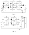
- Fig. 1a three bits or bridge devices B1, B2 and B3 are shown and are connected in series; the third bit B3 is connected to an output stage.
- the number of bridge devices may be lower or upper than three.
- the inductor of the conventional DC/DC Boost converter is replaced by "n" bridge devices connected in series.
- Each bridge device is composed of four switches and a capacitor as shown in Fig. 1a . It has to be noted here that two switches may be under the form of diodes acting as switches.
- This individual bridge structure is also called “bit”.
- the boost converter composed of three bridge devices also contains an output stage comprising a diode D4 and a switch S4.
- the bit B1 is composed of two diodes D11 and D12, two switches S11 and S12 and one capacitor C 1.
- the bit B2 is composed of two diodes D21 and D22, two switches S21 and S22 and one capacitor C2.
- the bit B3 is composed of two diodes D31 and D32, two switches S31 and S32 and one capacitor C3.
- the output stage is also connected to a capacitor CL.
- the anode of the diode Di1 is linked to the first terminal of the switch Si1.
- the cathode of Di1 is linked to the first terminal of the switch Si2 and to the positive terminal of the capacitor Ci.
- the second terminal of the switch Si1 is linked to the negative terminal of the capacitor Ci and to the anode of the diode Di2.
- the cathode of the diode Di2 is linked to the second terminal of the switch Si2.
- Electric DC providing means like photovoltaic elements PV provide an input voltage Vin.
- the positive terminal of electric DC providing means is connected to the anode of the diode D11.
- the cathode of the diode D12 is connected to the anode of the diode D21.
- the cathode of the diode D22 is connected to the anode of the diode D31.
- the cathode of the diode D32 is linked to the first terminal of the switch S4 and to the anode of the diode D4.
- the cathode of D4 is linked to the positive terminal of the capacitor CL.
- the second terminal of the switch S4 is linked to the negative terminal of the capacitor CL and to the negative terminal of electric DC providing means.
- the voltage on the capacitor CL is equal to Vout.
- Vb1 The difference of voltage between the input and the output of B1 is called Vb1
- Vb2 the difference of voltage between the input and the output of B2
- Vb3 the difference of voltage between the input and the output of B3
- Vc1 The difference of voltage in C1 is called Vc1
- Vc2 the difference of voltage in C2
- Vc3 the difference of voltage in C3
- n ratios 2 n
- n ratios the total number of possible step-up ratios (or duty-cycles) and "n” is the number of bits connected in series.
- Vc ⁇ 1 ⁇ : Vc ⁇ 2 ⁇ : Vcn 1 : 2 : ... 2 n - 1 ⁇ Vout / 2 n
- the switching pattern of the switches of each bridge Bi is defined so as to offer a voltage Vbi at the connectors of the bridge that equals + Vci, -Vci, or 0, where Vci is the voltage of the capacitor Ci.
- each capacitor has a charge and discharge pattern fixed for a given duty cycle, and different across capacitors, sometimes leading to high level of RMS current level passing through each bit. High RMS levels of current typically degrade the lifetime of the capacitors.
- the present invention aims to increase the number of different boost-ratios.
- the present invention proposes new switches control patterns for RLBC composed of plural bits, for example three bits B1, B2 and B3 and wherein the voltage values of at least one capacitor of a bit may be different when the selected periodical pattern is the at least one second periodical pattern or the at least one third periodical pattern.
- [Vc1:Vc2:Vc3] may be equal to [2:3:4]V ref if the selected periodical pattern is the at least one second periodical pattern
- [Vc1:Vc2:Vc3] may be equal to [1:2:4]V ref if the selected periodical pattern is the at least one third periodical pattern.
- A(t) represents the step function of time interval width ⁇ T.
- Si1 j and Si2 j are equal to one when the switches Silj and Si2 are in ON state or conductive state at the jth time interval Tj and are equal to null value when the switches Silj and Si2 are in OFF state or non conductive state at the jth time interval Tj.
- n is equal to the number of bits.
- V ref Vout N
- Finding a solution to the switching pattern of RLBC with n bits consists, for a given pair of integers ⁇ N, P ⁇ and a given vector K of integers in finding a matrix ( ⁇ ) of size (Nxn) and with elements in ⁇ -1; 0; 1 ⁇ such that
- the vector K of integers is [ 2 3 4 ] and each matrix disclosed in Figs. 5 to 9 verifies the conditions (i) and (ii).
- the vector K of integers is [ 1 2 4 ] and each matrix disclosed in Figs. 10 verifies the conditions (i) and (ii).
- Fig. 1b is a second example of boost converter composed of three bridge devices.
- the inductor of the conventional DC/DC Boost converter is replaced by "n" equal to three bridge devices connected in series.
- Each bridge device is composed of four switches and a capacitor as shown in Fig. 1 .
- This individual bridge structure is also called "bit”.
- the bit B1 is composed of two diodes D11 and D12, two switches S11 and S12 and one capacitor C1.
- the bit B2 is composed of two diodes D21 and D22, two switches S21 and S22 and one capacitor C2.
- the bit B3 is composed of two diodes D31 and D32', two switches S31 and S32' and one capacitor C3.
- the anode of the diode Di1 is linked to the first terminal of the switch Si1.
- the cathode of Di1 is linked to the first terminal of the switch Si2 and to the positive terminal of the capacitor Ci.
- the second terminal of the switch Si1 is linked to the negative terminal of the capacitor Ci and to the anode of the diode Di2.
- the cathode of the diode Di2 is linked to the second terminal of the switch Si2.
- the anode of the diode D31 is linked to the first terminal of the switch S31.
- the cathode of D31 is linked to the positive terminal of the capacitor C3 and to the anode of the diode D32'.
- the second terminal of the switch S31 is linked to the negative terminal of the capacitor C3 and to the first terminal of the switch S32'.
- Electric DC providing means like photovoltaic elements PV provide an input voltage Vin.
- the positive terminal of electric DC providing means is connected to the anode of the diode D11.
- the cathode of the diode D12 is connected to the anode of the diode D21.
- the cathode of the diode D22 is connected to the anode of the diode D31.
- the cathode of the diode D32' is connected to the positive terminal of the capacitor CL.
- the negative terminal of the capacitor CL and the second terminal of the switch S32' are connected to the negative terminal of electric DC providing means.
- the switch S32' acts similarly to switch S4 of Fig.1a and the diode D32' acts as diode D4 of Fig1a .
- the voltage on the capacitor CL is equal to Vout.
- Vb1 The difference of voltage between the input and the output of B1 is called Vb1
- Vb2 the difference of voltage between the input and the output of B2
- Vb3 the difference of voltage between the input and the output of B3 is called Vb3.
- Vb3 equals Vb3* when switch S32' is on, and equals Vb3** when switch S32' is off.
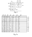
- Fig. 2 represents an example of a device comprising a boost converter composed of plural bridge devices.
- the device 20 has, for example, an architecture based on components connected together by a bus 201 and a processor 200 controlled by the program related to the algorithm as disclosed in the Fig. 11 .
- the device 20 is, in a variant, implemented under the form of one or several dedicated integrated circuits which execute the same operations as the one executed by the processor 200 as disclosed hereinafter.
- the bus 201 links the processor 200 to a read only memory ROM 202, a random access memory RAM 203, an analogue to digital converter ADC 206 and the RLBC module as the one disclosed in Figs. 1 .
- the read only memory ROM 202 contains instructions of the program related to the algorithm as disclosed in the Fig. 11 which are transferred, when the device 20 is powered on to the random access memory RAM 203.
- the read only memory ROM 202 memorizes the tables shown in Figs 3 to 10 of the present invention.
- the RAM memory 203 contains registers intended to receive variables, and the instructions of the program related to the algorithm as disclosed in the Fig. 11 .
- the analogue to digital converter 206 is connected to the RLBC and converts voltages representative of the input voltage Vin and/or the output voltage Vout into binary information.
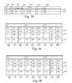
- Fig. 3a represents a table representing the different step-up ratios that can be provided by the first and at least one second periodical pattern according to the present invention when k 1 equals two, k 2 equals three and k 3 equals four.
- the table of the Fig. 3a comprises six columns noted 300 to 306.
- the column 300 shows different values of the input voltage Vin applied on the RLBC.
- the column 301 shows the output voltage Vout of the RLBC.
- the output voltage is for example equal to 240 Volts.
- the column 302 shows the different ratios between the output voltage Vout and the input voltage Vin.
- the column 303 shows the different duty cycles D of the RLBC.
- the column 304 shows the different values of the couples N and P.
- the column 305 shows the different values of the reference voltage V ref .
- the column 306 shows the Figs to be selected according to the input voltage value Vin.
- the input voltage is equal to 24 Volts
- the output voltage is 240 Volts
- the ratio Vout/Vin equals 10
- the duty cycle D equals 0.9
- the couple (N,P) equals (10,9)
- the reference voltage V ref equals 24 Volts
- the switching pattern to select in order to get the ratio of 10 is disclosed in the Fig. 5a .
- the input voltage is equal to 30 Volts
- the output voltage is 240 Volts
- the ratio Vout/Vin equals 8
- the duty cycle D equals 0.875
- the couple (N,P) equals (8,7)
- the reference voltage V ref equals 30 Volts
- the switching pattern to select in order to get the ratio of 8 is disclosed in the Fig. 6d .
- the input voltage is equal to 34.3 Volts
- the output voltage is 240 Volts
- the ratio Vout/Vin equals 7
- the duty cycle D equals 0.857
- the couple (N,P) equals (7,6)
- the reference voltage V ref equals 34.3 Volts
- the switching pattern to select in order to get the ratio of 7 is disclosed in the Fig. 7b .
- the input voltage is equal to 40 Volts
- the output voltage is 240 Volts
- the ratio Vout/Vin equals 6
- the duty cycle D equals 0.833
- the couple (N,P) equals (6,5)
- the reference voltage V ref equals 40 Volts
- the switching pattern to select in order to get the ratio of 6 is disclosed in the Fig. 8a .
- the input voltage is equal to 48 Volts
- the output voltage is 240 Volts
- the ratio Vout/Vin equals 5
- the duty cycle D equals 0.8
- the couple (N,P) equals (5,4)
- the reference voltage V ref 48 Volts
- the switching pattern to select in order to get the ratio of 5 is disclosed in the Fig. 9a .
- the input voltage is equal to 90 Volts
- the output voltage is 240 Volts
- the ratio Vout/Vin equals 2.67
- the duty cycle D equals 0.625
- the couple (N,P) equals (8,5)
- the reference voltage V ref equals 30 Volts
- the switching pattern to select in order to get the ratio of 2.67 is disclosed in the Fig. 6b .
- the input voltage is equal to 96 Volts
- the output voltage is 240 Volts
- the ratio Vout/Vin equals 2.5
- the duty cycle D equals 0.6
- the couple (N,P) equals (5,3)
- the reference voltage V ref 48 Volts and the switching pattern to select in order to get the ratio of 2.5 is disclosed in the Fig. 9b .
- the input voltage is equal to 144 Volts
- the output voltage is 240 Volts
- the ratio Vout/Vin equals 1.67
- the duty cycle D equals 0.4
- the couple (N,P) equals (5,2)
- the reference voltage V ref equals 48 Volts
- the switching pattern to select in order to get the ratio of 1.67 is disclosed in the Fig. 9c .
- the input voltage is equal to 150 Volts
- the output voltage is 240 Volts
- the ratio Vout/Vin equals 1.6
- the duty cycle D equals 0.375
- the couple (N,P) equals (8,3)
- the reference voltage V ref equals 30 Volts
- the switching pattern to select in order to get the ratio of 1.6 is disclosed in the Fig. 6c .
- the input voltage is equal to 192 Volts
- the output voltage is 240 Volts
- the ratio Vout/Vin equals 1.25
- the duty cycle D equals 0.2
- the couple (N,P) equals (5,1)
- the reference voltage V ref equals 48 Volts
- the switching pattern to select in order to get the ratio of 1.25 is disclosed in the Fig. 9d .
- the input voltage is equal to 200 Volts
- the output voltage is 240 Volts
- the ratio Vout/Vin equals 1.2
- the duty cycle D equals 0.166
- the couple (N,P) equals (6,1)
- the reference voltage V ref equals 40 Volts
- the switching pattern to select in order to get the ratio of 1.2 is disclosed in the Fig. 8b .
- the input voltage is equal to 205.7 Volts
- the output voltage is 240 Volts
- the ratio Vout/Vin equals 1.16
- the duty cycle D equals 0.142
- the couple (N,P) equals (7,1)
- the reference voltage V ref equals 34.3 Volts
- the switching pattern to select in order to get the ratio of 1.16 is disclosed in the Fig. 7a .
- the input voltage is equal to 210 Volts
- the output voltage is 240 Volts
- the ratio Vout/Vin equals 1.14
- the duty cycle D equals 0.125
- the couple (N,P) equals (8,1)
- the reference voltage V ref equals 30 Volts
- the switching pattern to select in order to get the ratio of 1.14 is disclosed in the Fig. 6a .
- the input voltage is equal to 216 Volts
- the output voltage is 240 Volts
- the ratio Vout/Vin equals 1.11
- the duty cycle D equals 0.1
- the couple (N,P) equals (10,1)
- the reference voltage V ref equals 24 Volts
- the switching pattern to select in order to get the ratio of 1.1 is disclosed in the Fig. 5b .
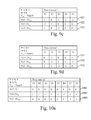
- Fig. 3b represents a table representing the different step-up ratios that can be provided by the at least one third periodical pattern according to the present invention when p 1 equals one, p 2 equals two and p 3 equals four.
- the table of the Fig. 3b comprises six columns noted 350 to 356.
- the column 350 shows different values of the input voltage Vin applied on the RLBC.
- the column 351 shows the output voltage Vout of the RLBC.
- the output voltage is for example equal to 240 Volts.
- the column 352 shows the different ratios between the output voltage Vout and the input voltage Vin.
- the column 353 shows the different duty cycles D of the RLBC.
- the column 354 shows the different values of the couples N and P.
- the column 355 shows the different values of the reference voltage V ref .
- the column 356 shows the Figs to be selected according to the input voltage value Vin.
- the input voltage is equal to 60 Volts
- the output voltage is 240 Volts
- the ratio Vout/Vin equals 4
- the duty cycle D equals 0. 75
- the couple (N,P) equals (8,6)
- the reference voltage V ref equals 30 Volts
- the switching pattern to select in order to get the ratio of 4 is disclosed in the Fig. 10a .
- the input voltage is equal to 48 Volts
- the output voltage is 240 Volts
- the ratio Vout/Vin equals 5
- the duty cycle D equals 0.8
- the couple (N,P) equals (5,4)
- the reference voltage V ref equals 30 Volts
- the switching pattern to select in order to get the ratio of 5 is disclosed in the Fig. 10b .
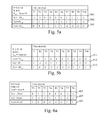
- Fig. 4a represents a table representing the switching states of the switches of the first example of boost converter shown in Fig. 1a in order to obtain different voltages on bridges of the boost converter composed of three bridge devices.
- the columns 400 to 402 are related to the bit B1
- the columns 403 to 405 are related to the bit B2
- the columns 406 to 408 are related to the bit B3.
- the line 411 shows that for a voltage Vb1 which is equal to Vc1, the switch S11 is in non conductive state and the switch S 12 is in non conductive state, for a voltage Vb2 which is equal to Vc2, the switch S21 is in non conductive state and the switch S22 is in non conductive state, for a voltage Vb3 which is equal to Vc3, the switch S31 is in non conductive state and the switch S32 is in non conductive state.
- the line 412 shows that for a voltage Vb 1 which is equal to null value, the switch S 11 is in non conductive state and the switch S 12 is in conductive state, for a voltage Vb2 which is equal to null value, the switch S21 is in non conductive state and the switch S22 is in conductive state, for a voltage Vb3 which is equal to null value, the switch S31 is in conductive state when the switch S32 is in non conductive state or the switch S31 is in non conductive state when the switch S32 is in conductive state.
- the line 413 shows that for a voltage Vb1 which is equal to -Vc1, the switch S11 is in conductive state and the switch S 12 is in conductive state, for a voltage Vb2 which is equal to -Vc2, the switch S21 is in conductive state and the switch S22 is in conductive state, for a voltage Vb3 which is equal to -Vc3, the switch S31 is in conductive state and the switch S32 is in conductive state.
- Fig. 4b represents a table representing the switching states of the switches of the second example of boost converter shown in Fig. 1b in order to obtain different voltages on bridges of the boost converter composed of three bridge devices.
- the columns 420 to 422 are related to the bit B1
- the columns 423 to 425 are related to the bit B2
- the columns 426 to 428 are related to the bit B3.
- the line 431 shows that for a voltage Vb1 which is equal to Vc1, the switch S11 is in non conductive state and the switch S 12 is in non conductive state, for a voltage Vb2 which is equal to Vc2, the switch S21 is in non conductive state and the switch S22 is in non conductive state, for a voltage Vb3 which is equal to Vc3, the switch S31 is in non conductive state and the switch S32' is in conductive state.
- the line 432 shows that for a voltage Vb1 equal to null value, the switch S11 is in non conductive state and the switch S12 is in conductive state, for a voltage Vb2 which is equal to null value, the switch S21 is in non conductive state and the switch S22 is in conductive state and for a voltage Vb3 which is equal to null value, the switches S31 and S32' are together either in conductive state or in non conductive state.
- the line 433 shows that for a voltage Vb1 which is equal to -Vc1, the switch S11 is in conductive state and the switch S 12 is in conductive state, for a voltage Vb2 which is equal to -Vc2, the switch S21 is in conductive state and the switch S22 is in conductive state, for a voltage Vb3 which is equal to -Vc3, the switch S31 is in conductive state and the switch S32' is in non conductive state.
- Figs. 5a and 5b are examples of voltage values on the bridges of the boost converter in order to have different step-up ratios when the first or at least one second periodical pattern is decomposed into ten time intervals.
- Vb1 -2V ref
- Vb1 2V ref
- Vb1 2V ref
- Vb1 2V ref
- T4 T5
- T8 T9 and T10
- Vb1 -2V ref
- Figs. 6a to 6d are examples of voltage values on the bridges of the boost converter composed of three bridge devices in order to have different step-up ratios when the first or at least one second periodical pattern is decomposed into eight time intervals.
- Vb1 -2V ref
- Vb1 2V ref
- Vb1 -2V ref
- Vb1 -2V ref
- Vb1 0
- Vb1 2V ref
- Figs. 7a and 7b are examples of voltage values on the bridges of the boost converter composed of three bridge devices in order to have different step-up ratios when the first or at least one second periodical pattern is decomposed into seven time intervals.
- T is the duration of the cycle operated by switch S4 of the Fig. 1a or by switch S32' of Fig1b .
- Vb1 2V ref
- Vb1 0
- Vb1 2V ref
- Vb1 -2V ref
- Vb1 2V ref
- Vb3 4V ref
- Vb1 -2V ref
- Figs. 8a and 8b are examples of voltage values on the bridges of the boost converter composed of three bridge devices in order to have different step-up ratios when the first or at least one second periodical pattern is decomposed into six time intervals.
- Vb1 2V ref
- Vb1 0
- Vb1 - 2 V ref
- Vb1 -2V ref
- Vb1 -2V ref
- Vb1 0
- Vb1 2V ref
- Figs. 9a to 9d are examples of voltage values on the bridges of the boost converter composed of three bridge devices in order to have different step-up ratios when the first or at least one second periodical pattern is decomposed into five time intervals.
- Vb1 2V ref
- Vb1 0
- Vb1 -2V ref
- Vb1 0
- Vb1 -2V ref
- Vb1 2V ref
- Vb1 0
- Vb1 - 2 V ref
- Vb1 2V ref
- Vb1 0
- Vb1 2V ref
- Vb1 -2V ref
- Vb1 -2V ref
- Figs. 10a and 10b are examples of voltage values on the bridges of the boost converter composed of three bridge devices in order to have different step-up ratios when the at least one third periodical pattern is selected.
- Vb2 2V ref
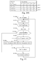
- Fig. 11 is an example of an algorithm for determining which periodical pattern has to be selected for the boost converter composed of n bridge devices according to the present invention.
- the present algorithm is executed by the device 20 comprising a boost converter composed of n bridge devices.
- the present algorithm may be executed by the processor 200.
- the processor 200 selects one first periodical pattern among available periodical patterns.
- the processor 200 gets the input voltage Vin that the boost converter composed of n bridge devices has to boost.
- Vin could be the result of a measurement made by digital converter 206 of the input voltage applied to the boost converter composed of n bridge devices.
- Vin could be determined by computation by processor 200 from yet other measurement made by digital converter 206 of other signals, such as bit voltages, output voltage, input or output currents, so as to realise a specific regulation function.
- the regulation function is determined so as to maximise the electrical power passing through the boost converter composed of n bridge devices.
- the processor 200 gets the desired range of output voltage in which the input voltage has to be boosted by the boost converter composed of n bridge devices.
- This range is composed of a first threshold V min , which is the minimum voltage value, and of a second threshold V max which is the maximum voltage value.
- V min the minimum voltage value
- V max the maximum voltage value.
- the desired range of output voltage is known in advance as the acceptable input range of the load equipment that is connected to the output of the boost converter composed of n bridge devices.
- the processor 200 gets an expected output voltage V out_ref to which the input voltage Vin has ideally to be boosted, using the currently selected periodical pattern, by the boost converter composed of n bridge devices within the desired range.
- the expected output voltage V out_ref is equal to V max .
- Vout is equal (V max +V min )/2.
- the processor 200 checks if a periodical pattern needs to be selected.
- the processor 200 checks if one of the duty cycle D selected at step S1105 corresponds to a one second periodical pattern, i.e. if one of the selected duty cycles D corresponds to a periodical pattern with same numbers k i as numbers k i of the first periodical pattern previously selected.
- step S1107 If one of the duty cycles D selected at step S1105 corresponds to a periodical pattern, the processor 200 moves to step S1107. Otherwise, the processor 200 moves to step S1106.
- the processor 200 selects one third periodical pattern wherein in each time interval, the voltage between the input and the output of each ith bridge device with i from one to n, is equal to a null value, or an integer number p i times a at least one third positive value, or minus the number p i times the at least one third positive value, at least one number k i being different from the number p i of the previously selected periodical pattern.
- the selected third periodical pattern corresponds to the duty cycle D for which the boosted voltage value V boost is the closest to the expected output voltage V out_ref within the desired range of output voltage [V min V max ].
- the processor 200 selects one second periodical pattern wherein in each time interval, the voltage between the input and the output of each ith bridge device with i from one to n, is equal to a null value, or an integer number k i times a at least one second positive value, or minus the number k i times the at least one second positive value.
- the selected second periodical pattern corresponds to the duty cycle D for which the boosted voltage value V boost is the closest to the expected output voltage V out_ref within the desired range of output voltage [V min V max ].
- the processor 200 sets the second periodical pattern selected at step S1107 or the third periodical pattern selected at step S1108 as a first periodical pattern stored in memory 202.
- the processor 200 commands the switches of the RLBC 205 according to the first periodical pattern stored in memory 202.
- the processor 200 commands the switches of the RLBC 205 according to a periodical pattern that results from a permutation of columns of the periodical pattern shown in the corresponding Fig among the Figs. 5 to 10 and stored in memory 202, which corresponds to the first periodical pattern.
- step S1109 the processor 200 commands the switches of the RLBC 205 according to the periodical pattern indicated in the Fig. 9a and returns to step S 1101.
- Other duty cycles indicated in Fig. 3a have corresponding boost voltage which are not comprised between the first and second thresholds.
- the processor 200 checks if one of the selected duty cycle D corresponds to a one second periodical pattern, i.e. if one of the selected duty cycles D corresponds to a periodical pattern with same numbers k i as numbers k i of the first periodical pattern previously selected.
- step S1106 selects the periodical pattern shown in Fig. 10a and moves to step S1108.
- the processor 200 sets the third periodical pattern selected at step S 1108 as a first periodical pattern.
- step S 1109 the processor 200 commands the switches of the RLBC 205 according to the periodical pattern indicated in the Fig. 10a and returns to step S 1101.
Priority Applications (6)
| Application Number | Priority Date | Filing Date | Title |
|---|---|---|---|
| EP09158617A EP2244363A1 (fr) | 2009-04-23 | 2009-04-23 | Procédé et appareil pour le contrôle de la tension de sortie d'un convertisseur élévateur |
| CN201080027943.3A CN102804572B (zh) | 2009-04-23 | 2010-04-22 | 用于控制升压转换器的输出电压的方法和设备 |
| EP10715230A EP2422437A2 (fr) | 2009-04-23 | 2010-04-22 | Procédé et appareil de commande de la tension de sortie d'un convertisseur survolteur |
| PCT/EP2010/055312 WO2010122084A2 (fr) | 2009-04-23 | 2010-04-22 | Procédé et appareil de commande de la tension de sortie d'un convertisseur survolteur |
| US13/265,733 US8873260B2 (en) | 2009-04-23 | 2010-04-22 | Method and an apparatus for controlling the output voltage of a boost converter |
| JP2012506487A JP5806206B2 (ja) | 2009-04-23 | 2010-04-22 | 昇圧コンバーターの出力電圧を制御する方法及び装置 |
Applications Claiming Priority (1)
| Application Number | Priority Date | Filing Date | Title |
|---|---|---|---|
| EP09158617A EP2244363A1 (fr) | 2009-04-23 | 2009-04-23 | Procédé et appareil pour le contrôle de la tension de sortie d'un convertisseur élévateur |
Publications (1)
| Publication Number | Publication Date |
|---|---|
| EP2244363A1 true EP2244363A1 (fr) | 2010-10-27 |
Family
ID=41131806
Family Applications (2)
| Application Number | Title | Priority Date | Filing Date |
|---|---|---|---|
| EP09158617A Withdrawn EP2244363A1 (fr) | 2009-04-23 | 2009-04-23 | Procédé et appareil pour le contrôle de la tension de sortie d'un convertisseur élévateur |
| EP10715230A Withdrawn EP2422437A2 (fr) | 2009-04-23 | 2010-04-22 | Procédé et appareil de commande de la tension de sortie d'un convertisseur survolteur |
Family Applications After (1)
| Application Number | Title | Priority Date | Filing Date |
|---|---|---|---|
| EP10715230A Withdrawn EP2422437A2 (fr) | 2009-04-23 | 2010-04-22 | Procédé et appareil de commande de la tension de sortie d'un convertisseur survolteur |
Country Status (5)
| Country | Link |
|---|---|
| US (1) | US8873260B2 (fr) |
| EP (2) | EP2244363A1 (fr) |
| JP (1) | JP5806206B2 (fr) |
| CN (1) | CN102804572B (fr) |
| WO (1) | WO2010122084A2 (fr) |
Families Citing this family (4)
| Publication number | Priority date | Publication date | Assignee | Title |
|---|---|---|---|---|
| US8259476B2 (en) * | 2008-07-29 | 2012-09-04 | Shmuel Ben-Yaakov | Self-adjusting switched-capacitor converter with multiple target voltages and target voltage ratios |
| EP2244368A1 (fr) * | 2009-04-23 | 2010-10-27 | Mitsubishi Electric R&D Centre Europe B.V. | Procédé et appareil pour le contrôle de la tension de sortie d'un convertisseur élévateur composé de plusieurs dispositifs ponts |
| KR101315143B1 (ko) * | 2012-08-22 | 2013-10-14 | 전북대학교산학협력단 | 높은 승압 비를 갖는 고효율 dc/dc 컨버터 |
| US9455645B1 (en) | 2013-03-13 | 2016-09-27 | The Florida State University Research Foundation, Inc. | System and method for leakage current suppression in a photovoltaic cascaded multilevel inverter |
Family Cites Families (14)
| Publication number | Priority date | Publication date | Assignee | Title |
|---|---|---|---|---|
| US3867643A (en) * | 1974-01-14 | 1975-02-18 | Massachusetts Inst Technology | Electric power converter |
| US5481447A (en) * | 1995-04-27 | 1996-01-02 | Fluke Corporation | Switched capacitance voltage multiplier with commutation |
| JP3424398B2 (ja) * | 1995-07-26 | 2003-07-07 | 松下電工株式会社 | 電力変換装置 |
| US5642275A (en) * | 1995-09-14 | 1997-06-24 | Lockheed Martin Energy System, Inc. | Multilevel cascade voltage source inverter with seperate DC sources |
| US6055168A (en) * | 1998-03-04 | 2000-04-25 | National Semiconductor Corporation | Capacitor DC-DC converter with PFM and gain hopping |
| JPH11299226A (ja) * | 1998-04-09 | 1999-10-29 | Fuji Electric Co Ltd | 直流電圧変換装置 |
| EP0992103B1 (fr) * | 1998-04-24 | 2008-10-29 | Nxp B.V. | Convertisseur elevateur-abaisseur de tension capacitive |
| US6169673B1 (en) * | 1999-01-27 | 2001-01-02 | National Semiconductor Corporation | Switched capacitor circuit having voltage management and method |
| US6563235B1 (en) * | 2000-10-03 | 2003-05-13 | National Semiconductor Corporation | Switched capacitor array circuit for use in DC-DC converter and method |
| BR0318551A (pt) * | 2003-10-17 | 2006-10-10 | Abb Research Ltd | circuito conversor para comutar um grande número de nìveis de tensão de comutação |
| US7456677B1 (en) * | 2006-05-01 | 2008-11-25 | National Semiconductor Corporation | Fractional gain circuit with switched capacitors and smoothed gain transitions for buck voltage regulation |
| US8212541B2 (en) * | 2008-05-08 | 2012-07-03 | Massachusetts Institute Of Technology | Power converter with capacitive energy transfer and fast dynamic response |
| US8089787B2 (en) * | 2008-06-27 | 2012-01-03 | Medtronic, Inc. | Switched capacitor DC-DC voltage converter |
| WO2010010710A1 (fr) * | 2008-07-24 | 2010-01-28 | 三菱電機株式会社 | Convertisseur de courant |
-
2009
- 2009-04-23 EP EP09158617A patent/EP2244363A1/fr not_active Withdrawn
-
2010
- 2010-04-22 WO PCT/EP2010/055312 patent/WO2010122084A2/fr active Application Filing
- 2010-04-22 CN CN201080027943.3A patent/CN102804572B/zh not_active Expired - Fee Related
- 2010-04-22 EP EP10715230A patent/EP2422437A2/fr not_active Withdrawn
- 2010-04-22 JP JP2012506487A patent/JP5806206B2/ja not_active Expired - Fee Related
- 2010-04-22 US US13/265,733 patent/US8873260B2/en not_active Expired - Fee Related
Non-Patent Citations (2)
| Title |
|---|
| ABUTBUL O ET AL: "Step-up switching-mode converter with high voltage gain using a switched-capacitor circuit", IEEE TRANSACTIONS ON CIRCUITS AND SYSTEMS PART I: REGULAR PAPERS, vol. 50, no. 8, 1 August 2003 (2003-08-01), IEEE SERVICE CENTER, NEW YORK, NY, US, pages 1098 - 1102, XP011099419, ISSN: 1057-7122 * |
| ZHONG DU, LEON M. TOLBERT, JOHN N. CHIASSON, BURAK ÖZPINECI: "A Cascade Multilevel Inverter Using a Single DC Source", IEEE, 23 March 2006 (2006-03-23), pages 426 - 430, XP002549964 * |
Also Published As
| Publication number | Publication date |
|---|---|
| EP2422437A2 (fr) | 2012-02-29 |
| US20120044726A1 (en) | 2012-02-23 |
| CN102804572B (zh) | 2015-04-01 |
| WO2010122084A3 (fr) | 2010-12-16 |
| US8873260B2 (en) | 2014-10-28 |
| CN102804572A (zh) | 2012-11-28 |
| JP5806206B2 (ja) | 2015-11-10 |
| JP2012525109A (ja) | 2012-10-18 |
| WO2010122084A2 (fr) | 2010-10-28 |
Similar Documents
| Publication | Publication Date | Title |
|---|---|---|
| US8982588B2 (en) | Method and an apparatus for controlling the output voltage of a boost converter composed of plural bridge devices | |
| US6636022B2 (en) | Controlled multi-output DC/DC converter | |
| US9929654B2 (en) | High voltage gain DC/DC power electronic converters | |
| KR100682006B1 (ko) | Dc-dc 컨버터 | |
| CN101771344B (zh) | 具有降压、升压和部分四开关模式的平均电流模式控制的转换器 | |
| US20120098514A1 (en) | Current mode switching regulator and control circuit and control method thereof | |
| EP2244363A1 (fr) | Procédé et appareil pour le contrôle de la tension de sortie d'un convertisseur élévateur | |
| EP2244364A1 (fr) | Procédé et appareil pour le contrôle des commutateurs d'un convertisseur élévateur composé de plusieurs dispositifs ponts | |
| EP2422449B1 (fr) | Procédé et appareil pour le contrôle du fonctionnement d'un circuit d'amortissement | |
| JP5517529B2 (ja) | 電力変換装置 | |
| Boora et al. | A new DC-DC converter with multi output: topology and control strategies | |
| Gopinathan et al. | Multistage high gain DC-DC converter topologies using SDLC network for DC microgrid | |
| Nagateja et al. | A single-inductor triple-output converter with an automatic detection of DC or AC energy harvesting source for supplying 93% efficiency and 0.05 mV/mA cross regulation to wearable electronics | |
| KR102335553B1 (ko) | Dc/dc 컨버터 | |
| EP2273659A1 (fr) | Procédé et appareil pour obtenir des informations activant la détermination du point d'alimentation maximum d'une source d'alimentation | |
| Nannam et al. | Comparative Analysis of Open Loop and Closed Loop Control of Dc-Dc Converter | |
| KR20230143858A (ko) | 전력변환장치 |
Legal Events
| Date | Code | Title | Description |
|---|---|---|---|
| PUAI | Public reference made under article 153(3) epc to a published international application that has entered the european phase |
Free format text: ORIGINAL CODE: 0009012 |
|
| AK | Designated contracting states |
Kind code of ref document: A1 Designated state(s): AT BE BG CH CY CZ DE DK EE ES FI FR GB GR HR HU IE IS IT LI LT LU LV MC MK MT NL NO PL PT RO SE SI SK TR |
|
| STAA | Information on the status of an ep patent application or granted ep patent |
Free format text: STATUS: THE APPLICATION IS DEEMED TO BE WITHDRAWN |
|
| 18D | Application deemed to be withdrawn |
Effective date: 20110428 |