WO2020246355A1 - Power conversion device - Google Patents
Power conversion device Download PDFInfo
- Publication number
- WO2020246355A1 WO2020246355A1 PCT/JP2020/021041 JP2020021041W WO2020246355A1 WO 2020246355 A1 WO2020246355 A1 WO 2020246355A1 JP 2020021041 W JP2020021041 W JP 2020021041W WO 2020246355 A1 WO2020246355 A1 WO 2020246355A1
- Authority
- WO
- WIPO (PCT)
- Prior art keywords
- phase
- period
- switching element
- carrier cycle
- command value
- Prior art date
Links
Images


Classifications
-
- H—ELECTRICITY
- H02—GENERATION; CONVERSION OR DISTRIBUTION OF ELECTRIC POWER
- H02M—APPARATUS FOR CONVERSION BETWEEN AC AND AC, BETWEEN AC AND DC, OR BETWEEN DC AND DC, AND FOR USE WITH MAINS OR SIMILAR POWER SUPPLY SYSTEMS; CONVERSION OF DC OR AC INPUT POWER INTO SURGE OUTPUT POWER; CONTROL OR REGULATION THEREOF
- H02M7/00—Conversion of ac power input into dc power output; Conversion of dc power input into ac power output
- H02M7/42—Conversion of dc power input into ac power output without possibility of reversal
- H02M7/44—Conversion of dc power input into ac power output without possibility of reversal by static converters
- H02M7/48—Conversion of dc power input into ac power output without possibility of reversal by static converters using discharge tubes with control electrode or semiconductor devices with control electrode
- H02M7/53—Conversion of dc power input into ac power output without possibility of reversal by static converters using discharge tubes with control electrode or semiconductor devices with control electrode using devices of a triode or transistor type requiring continuous application of a control signal
- H02M7/537—Conversion of dc power input into ac power output without possibility of reversal by static converters using discharge tubes with control electrode or semiconductor devices with control electrode using devices of a triode or transistor type requiring continuous application of a control signal using semiconductor devices only, e.g. single switched pulse inverters
- H02M7/539—Conversion of dc power input into ac power output without possibility of reversal by static converters using discharge tubes with control electrode or semiconductor devices with control electrode using devices of a triode or transistor type requiring continuous application of a control signal using semiconductor devices only, e.g. single switched pulse inverters with automatic control of output wave form or frequency
- H02M7/5395—Conversion of dc power input into ac power output without possibility of reversal by static converters using discharge tubes with control electrode or semiconductor devices with control electrode using devices of a triode or transistor type requiring continuous application of a control signal using semiconductor devices only, e.g. single switched pulse inverters with automatic control of output wave form or frequency by pulse-width modulation
-
- H—ELECTRICITY
- H02—GENERATION; CONVERSION OR DISTRIBUTION OF ELECTRIC POWER
- H02P—CONTROL OR REGULATION OF ELECTRIC MOTORS, ELECTRIC GENERATORS OR DYNAMO-ELECTRIC CONVERTERS; CONTROLLING TRANSFORMERS, REACTORS OR CHOKE COILS
- H02P27/00—Arrangements or methods for the control of AC motors characterised by the kind of supply voltage
- H02P27/04—Arrangements or methods for the control of AC motors characterised by the kind of supply voltage using variable-frequency supply voltage, e.g. inverter or converter supply voltage
- H02P27/06—Arrangements or methods for the control of AC motors characterised by the kind of supply voltage using variable-frequency supply voltage, e.g. inverter or converter supply voltage using dc to ac converters or inverters
- H02P27/08—Arrangements or methods for the control of AC motors characterised by the kind of supply voltage using variable-frequency supply voltage, e.g. inverter or converter supply voltage using dc to ac converters or inverters with pulse width modulation
-
- H—ELECTRICITY
- H02—GENERATION; CONVERSION OR DISTRIBUTION OF ELECTRIC POWER
- H02M—APPARATUS FOR CONVERSION BETWEEN AC AND AC, BETWEEN AC AND DC, OR BETWEEN DC AND DC, AND FOR USE WITH MAINS OR SIMILAR POWER SUPPLY SYSTEMS; CONVERSION OF DC OR AC INPUT POWER INTO SURGE OUTPUT POWER; CONTROL OR REGULATION THEREOF
- H02M1/00—Details of apparatus for conversion
- H02M1/0003—Details of control, feedback or regulation circuits
- H02M1/0009—Devices or circuits for detecting current in a converter
-
- H—ELECTRICITY
- H02—GENERATION; CONVERSION OR DISTRIBUTION OF ELECTRIC POWER
- H02M—APPARATUS FOR CONVERSION BETWEEN AC AND AC, BETWEEN AC AND DC, OR BETWEEN DC AND DC, AND FOR USE WITH MAINS OR SIMILAR POWER SUPPLY SYSTEMS; CONVERSION OF DC OR AC INPUT POWER INTO SURGE OUTPUT POWER; CONTROL OR REGULATION THEREOF
- H02M1/00—Details of apparatus for conversion
- H02M1/0048—Circuits or arrangements for reducing losses
- H02M1/0054—Transistor switching losses
-
- H—ELECTRICITY
- H02—GENERATION; CONVERSION OR DISTRIBUTION OF ELECTRIC POWER
- H02M—APPARATUS FOR CONVERSION BETWEEN AC AND AC, BETWEEN AC AND DC, OR BETWEEN DC AND DC, AND FOR USE WITH MAINS OR SIMILAR POWER SUPPLY SYSTEMS; CONVERSION OF DC OR AC INPUT POWER INTO SURGE OUTPUT POWER; CONTROL OR REGULATION THEREOF
- H02M1/00—Details of apparatus for conversion
- H02M1/08—Circuits specially adapted for the generation of control voltages for semiconductor devices incorporated in static converters
- H02M1/088—Circuits specially adapted for the generation of control voltages for semiconductor devices incorporated in static converters for the simultaneous control of series or parallel connected semiconductor devices
-
- H—ELECTRICITY
- H02—GENERATION; CONVERSION OR DISTRIBUTION OF ELECTRIC POWER
- H02M—APPARATUS FOR CONVERSION BETWEEN AC AND AC, BETWEEN AC AND DC, OR BETWEEN DC AND DC, AND FOR USE WITH MAINS OR SIMILAR POWER SUPPLY SYSTEMS; CONVERSION OF DC OR AC INPUT POWER INTO SURGE OUTPUT POWER; CONTROL OR REGULATION THEREOF
- H02M7/00—Conversion of ac power input into dc power output; Conversion of dc power input into ac power output
- H02M7/003—Constructional details, e.g. physical layout, assembly, wiring or busbar connections
-
- H—ELECTRICITY
- H02—GENERATION; CONVERSION OR DISTRIBUTION OF ELECTRIC POWER
- H02M—APPARATUS FOR CONVERSION BETWEEN AC AND AC, BETWEEN AC AND DC, OR BETWEEN DC AND DC, AND FOR USE WITH MAINS OR SIMILAR POWER SUPPLY SYSTEMS; CONVERSION OF DC OR AC INPUT POWER INTO SURGE OUTPUT POWER; CONTROL OR REGULATION THEREOF
- H02M7/00—Conversion of ac power input into dc power output; Conversion of dc power input into ac power output
- H02M7/42—Conversion of dc power input into ac power output without possibility of reversal
- H02M7/44—Conversion of dc power input into ac power output without possibility of reversal by static converters
- H02M7/48—Conversion of dc power input into ac power output without possibility of reversal by static converters using discharge tubes with control electrode or semiconductor devices with control electrode
- H02M7/53—Conversion of dc power input into ac power output without possibility of reversal by static converters using discharge tubes with control electrode or semiconductor devices with control electrode using devices of a triode or transistor type requiring continuous application of a control signal
- H02M7/537—Conversion of dc power input into ac power output without possibility of reversal by static converters using discharge tubes with control electrode or semiconductor devices with control electrode using devices of a triode or transistor type requiring continuous application of a control signal using semiconductor devices only, e.g. single switched pulse inverters
- H02M7/5387—Conversion of dc power input into ac power output without possibility of reversal by static converters using discharge tubes with control electrode or semiconductor devices with control electrode using devices of a triode or transistor type requiring continuous application of a control signal using semiconductor devices only, e.g. single switched pulse inverters in a bridge configuration
- H02M7/53871—Conversion of dc power input into ac power output without possibility of reversal by static converters using discharge tubes with control electrode or semiconductor devices with control electrode using devices of a triode or transistor type requiring continuous application of a control signal using semiconductor devices only, e.g. single switched pulse inverters in a bridge configuration with automatic control of output voltage or current
-
- H—ELECTRICITY
- H02—GENERATION; CONVERSION OR DISTRIBUTION OF ELECTRIC POWER
- H02P—CONTROL OR REGULATION OF ELECTRIC MOTORS, ELECTRIC GENERATORS OR DYNAMO-ELECTRIC CONVERTERS; CONTROLLING TRANSFORMERS, REACTORS OR CHOKE COILS
- H02P27/00—Arrangements or methods for the control of AC motors characterised by the kind of supply voltage
- H02P27/04—Arrangements or methods for the control of AC motors characterised by the kind of supply voltage using variable-frequency supply voltage, e.g. inverter or converter supply voltage
- H02P27/06—Arrangements or methods for the control of AC motors characterised by the kind of supply voltage using variable-frequency supply voltage, e.g. inverter or converter supply voltage using dc to ac converters or inverters
- H02P27/08—Arrangements or methods for the control of AC motors characterised by the kind of supply voltage using variable-frequency supply voltage, e.g. inverter or converter supply voltage using dc to ac converters or inverters with pulse width modulation
- H02P27/085—Arrangements or methods for the control of AC motors characterised by the kind of supply voltage using variable-frequency supply voltage, e.g. inverter or converter supply voltage using dc to ac converters or inverters with pulse width modulation wherein the PWM mode is adapted on the running conditions of the motor, e.g. the switching frequency
-
- H—ELECTRICITY
- H02—GENERATION; CONVERSION OR DISTRIBUTION OF ELECTRIC POWER
- H02P—CONTROL OR REGULATION OF ELECTRIC MOTORS, ELECTRIC GENERATORS OR DYNAMO-ELECTRIC CONVERTERS; CONTROLLING TRANSFORMERS, REACTORS OR CHOKE COILS
- H02P6/00—Arrangements for controlling synchronous motors or other dynamo-electric motors using electronic commutation dependent on the rotor position; Electronic commutators therefor
- H02P6/28—Arrangements for controlling current
-
- Y—GENERAL TAGGING OF NEW TECHNOLOGICAL DEVELOPMENTS; GENERAL TAGGING OF CROSS-SECTIONAL TECHNOLOGIES SPANNING OVER SEVERAL SECTIONS OF THE IPC; TECHNICAL SUBJECTS COVERED BY FORMER USPC CROSS-REFERENCE ART COLLECTIONS [XRACs] AND DIGESTS
- Y02—TECHNOLOGIES OR APPLICATIONS FOR MITIGATION OR ADAPTATION AGAINST CLIMATE CHANGE
- Y02B—CLIMATE CHANGE MITIGATION TECHNOLOGIES RELATED TO BUILDINGS, e.g. HOUSING, HOUSE APPLIANCES OR RELATED END-USER APPLICATIONS
- Y02B70/00—Technologies for an efficient end-user side electric power management and consumption
- Y02B70/10—Technologies improving the efficiency by using switched-mode power supplies [SMPS], i.e. efficient power electronics conversion e.g. power factor correction or reduction of losses in power supplies or efficient standby modes
Definitions
- the present invention relates to a power conversion device that supplies and drives a motor.
- a power conversion device for driving a motor controls the switching element of each UVW phase of a three-phase inverter circuit by PWM (Pulse With Modulation), but the position of the rotor (rotor) with a built-in permanent magnet is changed.
- PWM Pulse With Modulation
- one current detector shunt resistor or Hall element
- the phase current of two phases of UVW was detected from the switching timing of the switching element, and finally the phase current of each phase was obtained (see, for example, Patent Document 1).
- Patent Document 1 when the switching element on the upper arm side of the W phase is turned on for substantially the entire period within the carrier cycle and the switching element on the upper arm side of the V phase is turned off, the upper arm of the U phase is turned off. If the period during which the switching element on the side is turned on becomes shorter and the current detector becomes shorter than the minimum time required to detect the current, and the phase current for two phases cannot be detected, the two carriers The ON period of the switching element on the upper arm side of the U phase in the cycle was collected in one carrier cycle, and the correction was performed so that the current was not applied in the remaining carrier cycle (for example, FIG. 10B of Patent Document 1).
- the carrier frequency is halved because the U-phase switching elements are switched at every other carrier cycle.
- the carrier frequency is usually set to a value outside the audible region, there is a problem that noise is generated at a half carrier frequency.
- the present invention has been made to solve the above-mentioned conventional technical problems, and even if the motor rotates at a low speed and it becomes difficult to detect the direct current flowing through the inverter circuit, no noise is generated. It is an object of the present invention to provide a power conversion device capable of detecting a phase current without any trouble.
- the power conversion device of the present invention has an inverter circuit that drives a motor, a current detector that detects a DC current flowing through the inverter circuit, and a voltage command applied to the motor based on the current value detected by the current detector.
- a command value calculation unit that calculates a value
- a PWM signal generation unit that generates a PWM signal that PWM-controls the inverter circuit based on the voltage command value calculated by the command value calculation unit, and a PWM generated by the PWM signal generation unit. It is provided with a duty correction unit that corrects the duty of the signal, and the duty correction unit is used during the ON period of the switching element of the inverter circuit in a specific carrier cycle and the ON period of the switching element in another carrier cycle.
- a specific part is moved and added, or a part of the OFF period of the switching element in another carrier cycle is moved and added to the OFF period of the switching element in a specific carrier cycle. It is characterized in that the ON period or OFF period of the switching element in the carrier cycle is corrected so as to be equal to or longer than the minimum time required for detecting the current by the current detector.
- the power conversion device is characterized in that, in the above invention, the duty correction unit matches the sum of the duties in a specific carrier cycle and another carrier cycle before and after the correction.
- the power conversion device makes corrections such that the corrected ON period or OFF period of the switching element in another carrier cycle is the minimum value that can be output. It is characterized by doing.
- the power conversion device of the invention of claim 4 is characterized in that, in each of the above inventions, the duty correction unit provides a corrected ON period or OFF period of the switching element in the first half of a specific carrier cycle.
- the power conversion device is characterized in that, in the above invention, the duty correction unit provides a corrected ON period or OFF period of the switching element in the latter half of the other carrier cycle.
- the power conversion device has a duty correction unit that is specific when the voltage utilization rate, which is the root mean square of the normalized voltage command value of the motor, drops below a predetermined voltage utilization rate. It is characterized in that the ON period or the OFF period of the switching element in the carrier cycle and other carrier cycles is corrected.
- the command value calculation unit is based on the phase voltage command calculation unit that calculates the three-phase modulation voltage command value applied to the motor and the three-phase modulation voltage command value.
- a line modulation calculation unit that fixes the ON / OFF state of a predetermined one-phase switching element of the inverter circuit and calculates the two-phase modulation voltage command value that modulates the ON / OFF state of the other two-phase switching elements.
- the PWM signal generation unit is characterized in that it generates a PWM signal that PWM-controls the inverter circuit based on the two-phase modulation voltage command value calculated by the line modulation calculation unit.
- the OFF state of the switching element on the upper arm side of one phase of the inverter circuit is fixed, and the switching element on the upper arm side of the other two phases is fixed.
- the ON period is shorter than the minimum time in one carrier cycle, or the ON state of the switching element on the upper arm side of one phase is fixed, and the OFF period of the switching element on the upper arm side of the other two phases is one carrier.
- the ON period or the OFF period of the switching element in a specific carrier cycle and another carrier cycle is corrected.
- an inverter circuit for driving a motor, a current detector for detecting a DC current flowing through the inverter circuit, and a voltage command value applied to the motor based on the current value detected by the current detector.
- a command value calculation unit to be calculated a PWM signal generation unit that generates a PWM signal for PWM control of the inverter circuit based on the voltage command value calculated by the command value calculation unit, and a PWM signal generated by the PWM signal generation unit.
- the duty correction unit performs a part of the ON period of the switching element in another carrier cycle during the ON period of the switching element of the inverter circuit in a specific carrier cycle.
- the ON period or OFF period of the switching element in the above is equal to or longer than the minimum time required for detecting the current by the current detector, for example, the two-phase modulation method as in the invention of claim 7.
- the voltage utilization rate of the motor becomes low as in the invention of claim 6, and the OFF state of the switching element on the upper arm side of one phase of the inverter circuit is fixed as in the invention of claim 8.
- the ON period of the switching element on the upper arm side of the other two phases becomes shorter than the minimum time within one carrier cycle, or when the ON state of the switching element on the upper arm side of one phase is fixed, the other two Even when the OFF period of the switching element on the upper arm side of the phase becomes shorter than the minimum time within one carrier cycle, the ON period equal to or longer than the minimum time for current detection by the current detector in a specific carrier cycle, or , The OFF period can be secured and the phase current can be detected.
- the duty correction unit adds a part of the ON period or OFF period of the switching element in another carrier cycle to the ON period or OFF period of the switching element in a specific carrier cycle, the carrier frequency. It becomes possible to prevent the generation of noise due to the decrease in frequency.
- the duty correction unit makes the sum of the duties in the specific carrier cycle and the duty in the other carrier cycle match before and after the correction. It is possible to realize high-quality motor control without causing deterioration of motor controllability.
- the duty correction unit corrects the corrected ON period or OFF period of the switching element in another carrier cycle to the minimum value that can be output. Even if the motor rotates at a low speed, it is possible to secure an ON period or an OFF period of at least the minimum time for current detection by the current detector in a specific carrier cycle without any trouble.
- the duty correction unit provides a corrected ON period or OFF period of the switching element in the first half of the specific carrier cycle, and within another carrier cycle as in the invention of claim 5. If the corrected ON period or OFF period of the switching element is provided in the latter half of the above, the phase current can be easily achieved in a specific carrier cycle without overlapping the phases of the ON period or the OFF period with other phases. It will be possible to detect it.
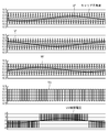
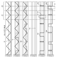
- FIG. 3 is a diagram showing a three-phase modulation voltage command value output by the phase voltage command calculation unit constituting the command value calculation unit of the control unit, a carrier triangle wave, a PWM waveform when performing three-phase modulation control, and a UV line voltage. is there. It is a figure which shows the two-phase modulation voltage command value output by the line modulation calculation unit which constitutes the command value calculation unit of the control unit of FIG. 1, the carrier triangle wave, the PWM waveform output by the PWM signal generation unit, and the UV line voltage. ..
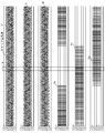
- FIG. 5 is a diagram showing a two-phase modulation voltage command value output by the line modulation calculation unit constituting the command value calculation unit of the control unit, a carrier triangle wave, a corrected PWM waveform output by the duty correction unit, and a line voltage. is there. It is an enlarged view around the frame X of FIG.
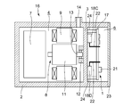
- the electric compressor 16 of the embodiment constitutes a part of a refrigerant circuit of a vehicle air conditioner mounted on a vehicle such as a hybrid vehicle or an electric vehicle, and is a DC power source (battery) mounted on the vehicle. ) 29 is fed and driven.
- FIG. 2 the inside of the metal housing 2 of the electric compressor 16 is divided into a compression mechanism accommodating portion 4 and an inverter accommodating portion 6 by a partition wall 3 intersecting the axial direction of the housing 2. It is partitioned, and for example, a scroll type compression mechanism 7 and a motor 8 for driving the compression mechanism 7 are housed in the compression mechanism accommodating portion 4.
- the motor 8 is an IPMSM (Interior Permanent Magnet Synchronous Motor) including a stator 9 fixed to the housing 2 and a rotor 11 having a built-in permanent magnet that rotates inside the stator 9.
- IPMSM Interior Permanent Magnet Synchronous Motor
- a bearing portion 12 is formed in the central portion of the partition wall 3 on the compression mechanism accommodating portion 4 side, one end of the drive shaft 13 of the rotor 11 is supported by the bearing portion 12, and the other end of the drive shaft 13 is a compression mechanism. It is connected to 7.
- a suction port 14 is formed in the vicinity of the partition wall 3 at a position corresponding to the compression mechanism accommodating portion 4 of the housing 2, and when the rotor 11 (drive shaft 13) of the motor 8 rotates to drive the compression mechanism 7.
- a refrigerant which is a working fluid, flows into the compression mechanism accommodating portion 4 of the housing 2 from the suction port 14, and is sucked into the compression mechanism 7 to be compressed.
- the refrigerant compressed by the compression mechanism 7 to a high temperature and high pressure is discharged to the refrigerant circuit outside the housing 2 from a discharge port (not shown). Further, the low-temperature refrigerant that has flowed in from the suction port 14 passes near the partition wall 3 and passes around the motor 8 and is sucked into the compression mechanism 7, so that the partition wall 3 is also cooled.
- the power conversion device 1 of the present invention that drives and controls the motor 8 is accommodated in the inverter accommodating portion 6 partitioned from the compression mechanism accommodating portion 4 by the partition wall 3.
- the power conversion device 1 is configured to supply power to the motor 8 via a sealed terminal or a lead wire penetrating the partition wall 3.
- the power conversion device 1 includes a substrate 17, six switching elements 18A to 18F wired on one surface side of the substrate 17, and the other surface side of the substrate 17. It is composed of a control unit 21 wired to the above, an HV connector (not shown), an LV connector, and the like.
- the switching elements 18A to 18F are composed of an insulated gate bipolar transistor (IGBT) or the like in which a MOS structure is incorporated in a gate portion.
- IGBT insulated gate bipolar transistor
- the switching element 18B and the switching element 18E on the lower arm side, the switching element 18C on the upper arm side and the switching element 18F on the lower arm side of the W-phase inverter 19W are arranged side by side.
- the switching elements 18A and 18D, the switching elements 18B and 18E, and the switching elements 18C and 18F are arranged radially around the center of the substrate 17.
- the terminal portions 22 of the switching elements 18A to 18F are connected to the substrate 17 in a state of being on the center side of the substrate 17. Then, the power conversion device 1 assembled in this way is housed in the inverter accommodating portion 6 in a state where one side of the switching elements 18A to 18F is on the partition wall 3 side, and is attached to the partition wall 3 to cover the power conversion device 1. It is closed at 23. In this case, the substrate 17 is fixed to the partition wall 3 via the boss portion 24 that stands up from the partition wall 3.
- the switching elements 18A to 18F are brought into close contact with the partition wall 3 directly or via a predetermined insulating heat conductive material, and are in close contact with the partition wall 3 of the housing 2. It becomes a heat exchange relationship. Since the partition wall 3 is cooled by the refrigerant sucked into the compression mechanism accommodating portion 4 as described above, the switching elements 18A to 18F have a heat exchange relationship with the suction refrigerant through the partition wall 3, and the partition wall It is cooled by the refrigerant sucked into the compression mechanism accommodating portion 4 through the thickness of 3, and the switching elements 18A to 18F themselves radiate heat to the refrigerant through the partition wall 3.
- the power conversion device 1 of the embodiment of the present invention includes the above-mentioned three-phase inverter circuit (three-phase inverter circuit) 28 and the control unit 21. I have.
- the inverter circuit 28 is a circuit that converts the DC voltage of the DC power supply (battery) 29 into a three-phase AC voltage and applies it to the armature coil of the stator 9 of the motor 8.
- the inverter circuit 28 has the above-mentioned U-phase inverter 19U, V-phase inverter 19V, and W-phase inverter 19W, and each phase inverter 19U to 19W has the above-mentioned switching elements 18A to 18C on the upper arm side, respectively.
- the switching elements 18D to 18F on the lower arm side are individually provided. Further, flywheel diodes 31 are connected in antiparallel to each of the switching elements 18A to 18F.
- the upper end side of the switching elements 18A to 18C on the upper arm side of the inverter circuit 28 is connected to the positive electrode side of the DC power supply 29 and the smoothing capacitor 32.
- the smoothing capacitor 32 is also provided on the substrate 17 to form the power conversion device 1.
- the lower end side of the switching elements 18D to 18F on the lower arm side of the inverter circuit 28 is connected to the negative electrode side of the DC power supply 29 and the smoothing capacitor 32.
- the switching element 18A on the upper arm side of the U-phase inverter 19U and the switching element 18D on the lower arm side are connected to the U-phase armature coil of the motor 8 to switch the V-phase inverter 19V on the upper arm side.
- the element 18B and the switching element 18E on the lower arm side are connected to the armature coil of the V phase of the motor 8, and the switching element 18C on the upper arm side and the switching element 18F on the lower arm side of the W phase inverter 19W are connected.
- the space is connected to the W-phase armature coil of the motor 8.
- a current detector 30 for detecting the DC current flowing through the inverter circuit 28 is connected to the bus between the DC power supply 29 and the inverter circuit 28.
- the current detector 30 is connected to the bus on the minus side in the embodiment, it may be connected to the bus on the plus side.
- the current detector 30 can be configured by a shunt resistor or a Hall element, but in the embodiment, it is assumed that the current detector 30 is composed of a shunt resistor.
- control unit 21 is composed of a microcomputer having a processor, inputs a rotation speed command value from the vehicle ECU, and receives U-phase current iu and V-phase current iv from the motor 8.
- Each phase current of the W phase current iw is input, and based on these, the ON / OFF states of the switching elements 18A to 18F of the inverter circuit 28 are controlled. Specifically, the gate voltage applied to the gate terminals of the switching elements 18A to 18F is controlled.
- the control unit 21 includes a phase current conversion unit 38, a phase voltage command calculation unit 33, a line modulation calculation unit 34, a PWM signal generation unit 36, a duty correction unit 39, and a gate driver 37. .. Then, the phase voltage command calculation unit 33 and the line modulation calculation unit 34 constitute the command value calculation unit 35 in the present invention.
- phase current conversion unit 38 is based on the direct current detected by the current detector 30 and the switching timing of the switching elements 18A to 18F, and the phase currents of the U-phase current iu, V-phase current iv, and W-phase current iw of the motor 8. Is detected.
- the switching element 18A on the upper arm side of the U-phase inverter 19U is turned on, the switching element 18E on the lower arm side of the V-phase inverter 19V and the switching element 18F on the lower arm side of the W-phase inverter 19W are turned on.
- the U-phase current iu flows from the switching element 18A to the U-phase armature coil of the motor 8
- the V-phase current iv flows from the flywheel diode 31 connected in parallel to the switching element 18E to the V-phase of the motor 8. It flows through the armature coil, and the W-phase current iw flows out from the W-phase armature coil of the motor 8 to the switching element 18F.
- a U-phase current iu flows through the current detector 30 and can be detected.
- the switching element 18A on the upper arm side of the U-phase inverter 19U and the switching element 18B on the upper arm side of the V-phase inverter 19V are turned on, and the switching element 18F on the lower arm side of the W-phase inverter 19W is turned on.
- the U-phase current iu and the V-phase current iv flow from the switching elements 18A and 18B to the U-phase and V-phase armature coils of the motor 8, respectively, and the W-phase current iw is the W-phase inverter of the motor 8. It flows out from the coil to the switching element 18F.
- a W-phase current iw flows through the current detector 30 and can be detected.
- the phase current conversion unit 38 has a minimum time Y required for detecting the phase current by the current detector 30, and the ON period of the switching elements 18A to 18C on the upper arm side within the carrier cycle, or the ON period of the switching elements 18A to 18C on the upper arm side, or If the OFF period is shorter than this minimum time Y, detection is impossible. Then, the phase currents iu, iv, and iwa detected by the phase current conversion unit 38 are input to the phase voltage command calculation unit 33.
- Phase voltage command calculation unit 33 (command value calculation unit 35)
- the phase voltage command calculation unit 33 applies a three-phase modulated voltage command value U'(U) to the armature coil of each phase of the motor 8 based on the electric angle and current command value of the motor 8 and the phase currents iu, iv, and iwa.
- Phase voltage command value V'(V phase voltage command value), W'(W phase voltage command value) are calculated.
- the three-phase modulation voltage command values U', V', and W' are after normalization of the voltage command value with the DC voltage Vdc when performing three-phase modulation control of the motor 8 (corrected to -1 to 1). It is the value of, and is shown in FIG.
- FIG. 3 also shows a carrier triangular wave to be compared by the PWM signal generation unit 36 described later.
- the frequency (carrier frequency) of the carrier triangular wave of the embodiment is set to 20 kHz outside the audible range. This is because when the carrier frequency becomes a frequency in the audible range lower than 20 kHz, the sound generated from the electric compressor 16 is recognized as noise.
- This carrier frequency is also a PWM signal (U phase) described later when Vu shown in FIG. 3 performs three-phase modulation control of the motor 8, and the UV line voltage in FIG. 3 is also three-phase modulation. It is a potential difference between the U phase and the V phase which will be described later when the control is performed.
- Line modulation calculation unit 34 (command value calculation unit 35)
- the line-to-line modulation calculation unit 34 is calculated by the phase voltage command calculation unit 33, and based on the calculated three-phase modulation voltage command values U', V', and W', the two-phase modulation voltage command value U (U-phase voltage command). Value), V (V-phase voltage command value), W (W-phase voltage command value) are calculated. The operation of the line modulation calculation unit 34 will be described in detail later.
- the PWM signal generation unit 36 is calculated by the line modulation calculation unit 34, and based on the calculated two-phase modulation voltage command values U, V, W, the U-phase inverter 19U, the V-phase inverter 19V, and the W phase of the inverter circuit 28
- the PWM signals Vu, Vv, and Vw, which are the drive command signals of the inverter 19W, are generated by comparing the magnitude with the carrier triangular wave.
- Duty correction unit 39 corrects the two-phase modulation voltage command values U, V, and W output from the line modulation calculation unit 34 (command value calculation unit 35), so that the PWM output from the PWM signal generation unit 36 is PWM.
- the signals Vu, Vv, and Vw are corrected and output to the gate driver 37, and the operation of the duty correction unit 39 will be described in detail later.
- Gate driver 37 Based on the PWM signals Vu, Vv, Vw output from the PWM signal generation unit 36, the gate driver 37 has the gate voltages Vu and Vul of the U-phase inverter 19U switching elements 18A and 18D, and the switching element 18B of the V-phase inverter 19V. , 18E gate voltages Vvu and Vvl, and gate voltages Vw and Vwl of the switching elements 18C and 18F of the W-phase inverter 19W are generated.
- These gate voltages Vuu, Vul, Vvu, Vvl, Vwoo, and Vwl can be represented by a duty (ON period of switching elements 18A to 18C on the upper arm side) which is a time ratio of the ON state in a predetermined time.
- each of the switching elements 18A to 18F of the inverter circuit 28 is ON / OFF driven based on the gate voltages Vuu, Vul, Vv, Vvl, Vwoo, and Vwl output from the gate driver 37. That is, when the gate voltage is in the ON state (predetermined voltage value), the transistor is turned on, and when the gate voltage is in the OFF state (zero), the transistor is turned off.
- the gate driver 37 is a circuit for applying a gate voltage to the IGBT based on the PWM signal, and is composed of a photocoupler, a logic IC, a transistor, and the like.
- the two-phase modulation voltage command values U, V, and W calculated by the line-to-line modulation calculation unit 34 are after normalization of the voltage command value for performing two-phase modulation control of the motor 8 with the DC voltage Vdc (-1 to 1 to). It is a value after correction to 1), and an example is shown in FIG. Note that FIG. 4 also shows a carrier triangular wave compared by the PWM signal generation unit 36 at the same time. Further, Vu shown in FIG. 4 is a PWM signal (U phase) for performing two-phase modulation control of the motor 8, and the UV line voltage in FIG. 4 is between U phase and V phase in two-phase modulation control. Is the potential difference of.
- the line-to-line modulation calculation unit 34 has a U-phase voltage command value U', a V-phase voltage command value V', and a W-phase voltage command, which are three-phase modulation voltage command values of each phase calculated by the phase voltage command calculation unit 33.
- the U-phase voltage command value U which is a two-phase modulation voltage command value for fixing the ON / OFF state of the switching elements 18A to 18F of the phase having the maximum absolute value to the ON / OFF state by comparing the values W', and V
- By calculating and outputting the phase voltage command value V and the W phase voltage command value W two-phase modulation control that reduces the number of switchings of the switching elements 18A to 18F compared to the case of performing three-phase modulation control is performed. Execute.
- the line modulation calculation unit 34 of the embodiment compares each value as shown in the following equations (i) to (iii). Set the values U'comp, V'comp, W'comp.
- U'comp U' ⁇ ⁇ ⁇ (i)
- V'comp V' ⁇ ⁇ ⁇ (ii)
- W'comp W' ⁇ ⁇ ⁇ (iii)
- the U-phase voltage command value U, the V-phase voltage command value V, and the W-phase voltage command value which are the two-phase modulation voltage command values, are used using the following equations (vi) to (viii).
- U U'-K + sign (K) ...
- V V'-K + sign (K) ...
- W W'-K + sign (K) ... (viii)
- sign (K) is defined as "1" when K is a positive value and "-1" when K is a negative value.
- V-phase voltage command value V' is K and the comparison value V'comp is the maximum value K1
- the V-phase voltage command value V becomes "1"
- the comparison value V'comp is the minimum value K2.
- the V-phase voltage command value V becomes “-1”.
- the ON / OFF states of the switching elements 18B and 18E of the V-phase inverter 19V are fixed during the period when the V-phase voltage command value V'is K, and the number of switchings is reduced accordingly.
- the W-phase voltage command value W'is K and the comparison value W'comp is the maximum value K1
- the W-phase voltage command value W becomes "1"
- the comparison value W'comp is the minimum value K2.
- the W-phase voltage command value W becomes “-1”.
- the ON / OFF states of the switching elements 18C and 18F of the W-phase inverter 19W are fixed during the period when the W-phase voltage command value W'is K, and the number of switchings is reduced accordingly.
- FIG. 4 shows a U-phase voltage command value U, a V-phase voltage command value V, and a W-phase voltage command value W output from the line modulation calculation unit 34, and a U-phase PWM signal Vu output from the PWM signal generation unit 36. And the UV line voltage.
- FIG. 5 shows the two-phase modulation voltage command values U, V, W output by the line modulation calculation unit 34, the carrier triangle wave, and the PWM signals Vu, Vv, Vw output by the PWM signal generation unit 36
- FIG. 6 shows FIG. An enlarged view of the vicinity of the frame X inside is shown.
- FIGS. 5 to 8 is a two-phase modulation control in which the switching element on the upper arm side of any one phase is fixed in the OFF state and the switching element on the lower arm side is fixed in the ON state.
- the PWM signal Vu is a drive command signal for the U-phase inverter 19U of the inverter circuit 28, and the pulse width of “1” shown in FIGS. 5 and 6 is the duty within one carrier cycle. It is the ON period of the switching element 18A on the arm side. That is, during this duty (width of the pulse of "1"), the switching element 18A on the upper arm side is turned on, and the switching element 18D on the lower arm side is turned off.
- the PWM signal Vv is a drive command signal of the V-phase inverter 19V
- the width of the pulse of "1" shown in FIGS. 5 and 6 is the duty within one carrier cycle, and is on the upper arm side.
- the ON period of the switching element 18B is reached. That is, during this duty (width of the pulse of "1"), the switching element 18B on the upper arm side is turned on, and the switching element 18E on the lower arm side is turned off.
- the PWM signal Vw is a drive command signal of the W-phase inverter 19W
- the width of the pulse of “1” shown in FIGS. 5 and 6 is the duty within one carrier cycle, and is on the upper arm side.
- the ON period of the switching element 18C is reached. That is, during this duty (width of the pulse of "1"), the switching element 18C on the upper arm side is turned on, and the switching element 18F on the lower arm side is turned off.
- the switching element 18A on the upper arm side of the U phase is fixed in the OFF state. Then, when the phase current is detected during the ON period of the switching elements 18B and 18C on the upper arm side of the V phase and the W phase, as shown in FIG. 6, the switching elements 18B and 18C on the upper arm side within one carrier cycle. When the ON period of is shorter than this minimum time Y, it becomes impossible to detect the phase currents of the V phase and the W phase.
- the U-phase current iu can be detected, the V-phase current iv and the W-phase current iwa cannot be detected, so that the three-phase phase currents iu, iv, and iwa cannot be detected.
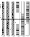
- the duty correction unit 39 of the control unit 21 receives a line modulation calculation unit 34 (command) as shown in FIGS. 7 and 8 when the voltage utilization rate kH of the motor 8 drops to a predetermined voltage utilization rate kH1 or less.
- the two-phase modulation voltage command values U, V, and W output from the value calculation unit 35) are corrected, and the PWM signals Vu, Vv, and Vw output from the PWM signal generation unit 36 are corrected.
- the ON period (indicated by P1 in FIG. 8) of the switching element 18B having a specific carrier period Z1 of the V phase is corrected to be equal to or longer than the above-mentioned minimum time Y.
- the ON period (indicated by P2 in FIG. 8) of the switching element 18B having the carrier period Z2 of the V phase is set to the minimum value that can be output.
- the duty correction unit 39 sets the sum of the duties of the switching elements 18B in the corrected two carrier cycles (Z1 to Z2) shown in FIG. 8 into the two carrier cycles (Z1 to Z2) before the correction in FIG. Matches the sum of the duties of the switching element 18B in. Further, the duty correction unit 39 provides the ON period of the switching element 18B in the first half of the specific carrier period Z1 of the V phase, and provides the ON period of the switching element 18B in the latter half of the other carrier period Z2 of the V phase.
- the duty correction unit 39 also performs another carrier cycle of the W phase (next carrier cycle of Z2) during the ON period of the switching element 18C on the upper arm side of the W phase of the specific carrier cycle Z2 of the W phase. ), By moving and adding a part of the ON period of the switching element 18C, the ON period of the switching element 18C of the specific carrier period Z2 of the W phase (indicated by P3 in FIG. 8) is set to the above-mentioned minimum time. Make corrections that are Y or greater. On the other hand, the ON period of the switching element 18C having another carrier cycle of the W phase is set to the minimum value that can be output in the same manner.
- the duty correction unit 39 sets the sum of the duties of the switching element 18C in the corrected two carrier cycles (Z2 and the next cycle) shown in FIG. 8 as the two carrier cycles before the correction in FIG. It is matched with the sum of the duties of the switching element 18C at (Z2 and the next cycle). Further, the duty correction unit 39 provides the ON period of the switching element 18C in the first half of the specific carrier period Z2 of the W phase, and ONs the switching element 18C in the latter half of the other carrier period of the W phase (the cycle next to Z2). Set a period.
- the above correction is similarly executed for other timings (a set of a specific carrier cycle and another carrier cycle).
- the other carrier cycle is not limited to one, and a part of each of those ON periods is moved from two or more (plural) carrier cycles following the specific carrier cycle to the ON period of the specific carrier cycle. It may be.
- the phase current converter 38 can detect the V-phase current iv in the carrier cycle Z1 and the W-phase current iv in the carrier cycle Z2 by the current detector 30, and finally three-phase. It is possible to detect the minute phase currents iu, iv, and iwa. In this case, for example, since the ON period of the switching element 18B and the ON period of the switching element 18C in the carrier cycle Z2 do not overlap, the V-phase current iv and the W-phase current iwa can be detected without any trouble.
- the duty correction unit 39 of the control unit 21 performs another carrier during the ON period of the switching element (18B in the V phase) of the inverter circuit 28 in a specific carrier cycle (Z1 in the V phase).
- the switching element (Z1 in V phase) in a specific carrier period (Z1 in V phase) is added.
- the ON period of 18B is corrected to be equal to or longer than the minimum time Y required for detecting the current by the current detector 30, for example, in the power conversion device 1 of the two-phase modulation method as in the embodiment, As in the embodiment, the voltage utilization rate kH of the motor 8 becomes low, the OFF state of the switching element 18A on the upper arm side of the U phase of the inverter circuit 28 is fixed, and the OFF state of the upper arm side of the other two phases is fixed. Even when the ON period of the switching elements 18B and 18C is shorter than the minimum time Y within one carrier cycle, the minimum time Y or more for current detection by the current detector 30 in a specific carrier cycle (Z1 in the V phase). The ON period is secured, and the phase current (iv in the carrier cycle Z1 of the V phase) can be detected.
- the duty correction unit 39 sets a part of the ON period of the switching element (18B in the V phase) in another carrier period (Z2 in the V phase) to the switching element (Z1 in the V phase) having a specific carrier period (Z1 in the V phase). Since it is added to the ON period of 18B), it is possible to prevent the generation of noise due to the decrease in the carrier frequency.
- the duty correction unit 39 makes the sum of the duties in the specific carrier cycle (Z1 in the V phase) and the duty in the other carrier cycle (Z2 in the V phase) match before and after the correction. Therefore, it is possible to realize high-quality motor control without causing deterioration of the controllability of the motor 8.
- the duty correction unit 39 corrects the corrected ON period of the switching element (18B in the V phase) in another carrier cycle (Z2 in the V phase) to be the minimum value that can be output. Therefore, even if the motor 8 rotates at a low speed, it is possible to secure an ON period of Y or more, which is the minimum time for current detection by the current detector 30, in a specific carrier cycle (Z1 in the V phase) without any problem. Will be.
- the duty correction unit 39 provides a corrected ON period of the switching element (18B in the V phase) in the first half of the specific carrier cycle (Z1 in the V phase), and provides another carrier cycle (Z1 in the V phase). Since the corrected ON period of the switching element (18B in the V phase) is provided in the latter half of Z2), the phase of the ON period does not overlap with other phases, and a specific carrier period (Z1 in the V phase) is provided. , In the W phase, the phase currents iv and iwa can be easily detected in Z2)).
- a part of the ON period of the switching element in another carrier cycle is moved and added to the ON period of the switching element of the inverter circuit 28 in a specific carrier cycle.
- the phase switching element is fixed in the ON state and the other two-phase switching element is switched, the OFF period of the switching element in a specific carrier cycle and the OFF period of the switching element in the other carrier cycle
- the OFF period of the switching element in a specific carrier cycle may be corrected to be equal to or longer than the minimum time Y required for detecting the current by the current detector 30. ..
- the present invention has been described with the two-phase modulation type power conversion device 1 in which the one-phase switching element is fixed in the OFF state and the other two-phase switching elements are switched, but the present invention is not limited to this.
- the present invention is also effective in a method of fixing the switching element of the above to the ON state and the OFF state.
- the duty correction unit corrects the three-phase modulation voltage command values U', V', and W'output by the phase voltage command calculation unit 33 in the same manner as described above.
- the present invention is applied to the power converter 1 that drives and controls the motor 8 of the electric compressor 16, but the present invention is not limited to this, and the present invention is effective for the drive control of the motors of various devices.
- Power converter 8 Motor 16 Electric compressor 18A-18F Switching element 19U U-phase inverter 19V V-phase inverter 19W W-phase inverter 21 Control unit 28 Three-phase inverter circuit 30 Current detector 33 Phase voltage command calculation unit 34 Line modulation calculation Part 35 Command value calculation part 36 PWM signal generation part 37 Gate driver 38 Phase current conversion part 39 Duty correction part
Abstract
[Problem] To provide a power conversion device which can detect phase current without generating noise and without hindrance, even in situations in which motor speed is low and DC current in an inverter circuit is difficult to detect. During the ON period of switching elements 18B, 18C of an inverter circuit 28 in a specific carrier cycle, a duty correction unit 39 for correcting the duty of a PWM signal corrects the ON period of the switching elements in the specific carrier cycle to at least the minimum time Y necessary for the current detector 30 to detect the current, by moving and adding part of the ON periods of said switching elements 18B, 18C in another carrier cycle.
Description
本発明は、モータに電力を供給して駆動する電力変換装置に関するものである。
The present invention relates to a power conversion device that supplies and drives a motor.
従来よりモータを駆動するための電力変換装置は、三相インバータ回路のUVW各相のスイッチング素子をPWM(Pulse Width Modulation)制御するものであるが、永久磁石内蔵のロータ(回転子)の位置を推定する情報となる相電流を検出するために、直流電源とインバータ回路の間の直流電流を検出する電流検出器(シャント抵抗やホール素子)を一つ設け、この電流検出器が検出する直流電流とスイッチング素子のスイッチングタイミングからUVWのうちの二相の相電流を検出し、最終的に各相の相電流を求めていた(例えば、特許文献1参照)。
Conventionally, a power conversion device for driving a motor controls the switching element of each UVW phase of a three-phase inverter circuit by PWM (Pulse With Modulation), but the position of the rotor (rotor) with a built-in permanent magnet is changed. In order to detect the phase current that is the information to be estimated, one current detector (shunt resistor or Hall element) that detects the DC current between the DC power supply and the inverter circuit is provided, and the DC current detected by this current detector is provided. The phase current of two phases of UVW was detected from the switching timing of the switching element, and finally the phase current of each phase was obtained (see, for example, Patent Document 1).
また、近年ではスイッチング素子の損失と発熱を低減する目的で、このPWM制御部に二相変調と称される方式を適用した電力変換装置(インバータ装置)も提案されている。この二相変調方式の電力変換装置は、UVWの各相のうち何れか一相のON/OFF状態を固定し、他の二相のみON/OFF状態を変調させながら制御することにより、三相変調方式よりもスイッチング素子のスイッチング回数を減少させ、スイッチング損失と発熱量を減少させつつ、PWM制御するものであった(例えば、特許文献2参照)。
Further, in recent years, a power conversion device (inverter device) in which a method called two-phase modulation is applied to this PWM control unit has been proposed for the purpose of reducing loss and heat generation of switching elements. This two-phase modulation type power conversion device fixes the ON / OFF state of any one of the UVW phases, and controls only the other two phases while modulating the ON / OFF state, thereby performing three phases. Compared to the modulation method, the number of switchings of the switching element is reduced, and the switching loss and the amount of heat generated are reduced while performing PWM control (see, for example, Patent Document 2).
ここで、前記特許文献1ではW相の上アーム側のスイッチング素子がキャリア周期内の略全期間ONされ、V相の上アーム側のスイッチング素子はOFFされているときに、U相の上アーム側のスイッチング素子がONされている期間が短くなって、電流検出器が電流を検出するために必要な最小時間よりも短くなり、二相分の相電流を検出できなくなった場合、二つのキャリア周期でのU相の上アーム側のスイッチング素子のON期間を一つのキャリア周期に集め、残りのキャリア周期では通電しない補正を行っていた(例えば、特許文献1の図10(b))。
Here, in Patent Document 1, when the switching element on the upper arm side of the W phase is turned on for substantially the entire period within the carrier cycle and the switching element on the upper arm side of the V phase is turned off, the upper arm of the U phase is turned off. If the period during which the switching element on the side is turned on becomes shorter and the current detector becomes shorter than the minimum time required to detect the current, and the phase current for two phases cannot be detected, the two carriers The ON period of the switching element on the upper arm side of the U phase in the cycle was collected in one carrier cycle, and the correction was performed so that the current was not applied in the remaining carrier cycle (for example, FIG. 10B of Patent Document 1).
しかしながら、上記のような補正を行った場合、U相のスイッチング素子を一つ置きのキャリア周期でスイッチングすることになるため、キャリア周波数は二分の一となる。一方、キャリア周波数は通常、可聴領域を外した値としているため、二分の一のキャリア周波数では騒音が生じてしまう問題があった。
However, when the above correction is performed, the carrier frequency is halved because the U-phase switching elements are switched at every other carrier cycle. On the other hand, since the carrier frequency is usually set to a value outside the audible region, there is a problem that noise is generated at a half carrier frequency.
本発明は、係る従来の技術的課題を解決するために成されたものであり、モータが低回転となってインバータ回路に流れる直流電流を検出し難い状況となっても、騒音を生じること無く支障無く相電流を検出することができるようにした電力変換装置を提供するものである。
The present invention has been made to solve the above-mentioned conventional technical problems, and even if the motor rotates at a low speed and it becomes difficult to detect the direct current flowing through the inverter circuit, no noise is generated. It is an object of the present invention to provide a power conversion device capable of detecting a phase current without any trouble.
本発明の電力変換装置は、モータを駆動するインバータ回路と、このインバータ回路に流れる直流電流を検出する電流検出器と、この電流検出器が検出する電流値に基づいて、モータに印加する電圧指令値を演算する指令値演算部と、この指令値演算部が演算した電圧指令値に基づき、インバータ回路をPWM制御するPWM信号を生成するPWM信号生成部と、このPWM信号生成部が生成したPWM信号のデューティを補正するデューティ補正部を備えたものであって、デューティ補正部は、特定のキャリア周期におけるインバータ回路のスイッチング素子のON期間に、他のキャリア周期での当該スイッチング素子のON期間の一部を移動して加算すること、又は、特定のキャリア周期におけるスイッチング素子のOFF期間に、他のキャリア周期での当該スイッチング素子のOFF期間の一部を移動して加算することで、特定のキャリア周期におけるスイッチング素子のON期間、又は、OFF期間を、電流検出器によって電流を検出するために必要な最小時間以上とする補正を行うことを特徴とする。
The power conversion device of the present invention has an inverter circuit that drives a motor, a current detector that detects a DC current flowing through the inverter circuit, and a voltage command applied to the motor based on the current value detected by the current detector. A command value calculation unit that calculates a value, a PWM signal generation unit that generates a PWM signal that PWM-controls the inverter circuit based on the voltage command value calculated by the command value calculation unit, and a PWM generated by the PWM signal generation unit. It is provided with a duty correction unit that corrects the duty of the signal, and the duty correction unit is used during the ON period of the switching element of the inverter circuit in a specific carrier cycle and the ON period of the switching element in another carrier cycle. A specific part is moved and added, or a part of the OFF period of the switching element in another carrier cycle is moved and added to the OFF period of the switching element in a specific carrier cycle. It is characterized in that the ON period or OFF period of the switching element in the carrier cycle is corrected so as to be equal to or longer than the minimum time required for detecting the current by the current detector.
請求項2の発明の電力変換装置は、上記発明においてデューティ補正部は、特定のキャリア周期と他のキャリア周期でのデューティの和を、補正前と補正後で一致させることを特徴とする。
The power conversion device according to the second aspect of the present invention is characterized in that, in the above invention, the duty correction unit matches the sum of the duties in a specific carrier cycle and another carrier cycle before and after the correction.
請求項3の発明の電力変換装置は、上記各発明においてデューティ補正部は、他のキャリア周期でのスイッチング素子の補正されたON期間、又は、OFF期間を、出力可能な最小値とする補正を行うことを特徴とする。
In each of the above inventions, the power conversion device according to the third aspect of the present invention makes corrections such that the corrected ON period or OFF period of the switching element in another carrier cycle is the minimum value that can be output. It is characterized by doing.
請求項4の発明の電力変換装置は、上記各発明においてデューティ補正部は、特定のキャリア周期内の前半にスイッチング素子の補正されたON期間、又は、OFF期間を設けることを特徴とする。
The power conversion device of the invention of claim 4 is characterized in that, in each of the above inventions, the duty correction unit provides a corrected ON period or OFF period of the switching element in the first half of a specific carrier cycle.
請求項5の発明の電力変換装置は、上記発明においてデューティ補正部は、他のキャリア周期内の後半にスイッチング素子の補正されたON期間、又は、OFF期間を設けることを特徴とする。
The power conversion device according to the fifth aspect of the present invention is characterized in that, in the above invention, the duty correction unit provides a corrected ON period or OFF period of the switching element in the latter half of the other carrier cycle.
請求項6の発明の電力変換装置は、上記各発明においてデューティ補正部は、モータの正規化した電圧指令値の二乗平均である電圧利用率が所定電圧利用率以下に低下した場合に、特定のキャリア周期及び他のキャリア周期におけるスイッチング素子のON期間、又は、OFF期間の補正を行うことを特徴とする。
In each of the above inventions, the power conversion device according to the invention of claim 6 has a duty correction unit that is specific when the voltage utilization rate, which is the root mean square of the normalized voltage command value of the motor, drops below a predetermined voltage utilization rate. It is characterized in that the ON period or the OFF period of the switching element in the carrier cycle and other carrier cycles is corrected.
請求項7の発明の電力変換装置は、上記各発明において指令値演算部は、モータに印加する三相変調電圧指令値を演算する相電圧指令演算部と、三相変調電圧指令値に基づき、インバータ回路の所定の一相のスイッチング素子のON/OFF状態を固定させると共に、他の二相のスイッチング素子のON/OFF状態を変調させる二相変調電圧指令値を演算する線間変調演算部を有し、PWM信号生成部は、線間変調演算部が演算する二相変調電圧指令値に基づき、インバータ回路をPWM制御するPWM信号を生成することを特徴とする。
In the power conversion device of the invention of claim 7, in each of the above inventions, the command value calculation unit is based on the phase voltage command calculation unit that calculates the three-phase modulation voltage command value applied to the motor and the three-phase modulation voltage command value. A line modulation calculation unit that fixes the ON / OFF state of a predetermined one-phase switching element of the inverter circuit and calculates the two-phase modulation voltage command value that modulates the ON / OFF state of the other two-phase switching elements. The PWM signal generation unit is characterized in that it generates a PWM signal that PWM-controls the inverter circuit based on the two-phase modulation voltage command value calculated by the line modulation calculation unit.
請求項8の発明の電力変換装置は、上記発明においてデューティ補正部は、インバータ回路の一相の上アーム側のスイッチング素子のOFF状態が固定され、他の二相の上アーム側のスイッチング素子のON期間が1キャリア周期内において前記最小時間より短い場合、又は、一相の上アーム側のスイッチング素子のON状態が固定され、他の二相の上アーム側のスイッチング素子のOFF期間が1キャリア周期内において前記最小時間より短い場合、特定のキャリア周期及び他のキャリア周期におけるスイッチング素子のON期間、又は、OFF期間の補正を行うことを特徴とする。
In the power conversion device of the invention of claim 8, in the above invention, in the duty correction unit, the OFF state of the switching element on the upper arm side of one phase of the inverter circuit is fixed, and the switching element on the upper arm side of the other two phases is fixed. When the ON period is shorter than the minimum time in one carrier cycle, or the ON state of the switching element on the upper arm side of one phase is fixed, and the OFF period of the switching element on the upper arm side of the other two phases is one carrier. When the time is shorter than the minimum time in the cycle, the ON period or the OFF period of the switching element in a specific carrier cycle and another carrier cycle is corrected.
本発明によれば、モータを駆動するインバータ回路と、このインバータ回路に流れる直流電流を検出する電流検出器と、この電流検出器が検出する電流値に基づいて、モータに印加する電圧指令値を演算する指令値演算部と、この指令値演算部が演算した電圧指令値に基づき、インバータ回路をPWM制御するPWM信号を生成するPWM信号生成部と、このPWM信号生成部が生成したPWM信号のデューティを補正するデューティ補正部を備えた電力変換装置において、デューティ補正部が、特定のキャリア周期におけるインバータ回路のスイッチング素子のON期間に、他のキャリア周期での当該スイッチング素子のON期間の一部を移動して加算すること、又は、特定のキャリア周期におけるスイッチング素子のOFF期間に、他のキャリア周期での当該スイッチング素子のOFF期間の一部を移動して加算することで、特定のキャリア周期におけるスイッチング素子のON期間、又は、OFF期間を、電流検出器によって電流を検出するために必要な最小時間以上とする補正を行うようにしたので、例えば請求項7の発明の如き二相変調方式の電力変換装置において、請求項6の発明の如くモータの電圧利用率が低くなって、請求項8の発明の如く例えばインバータ回路の一相の上アーム側のスイッチング素子のOFF状態が固定され、他の二相の上アーム側のスイッチング素子のON期間が1キャリア周期内において前記最小時間より短くなった場合、又は、一相の上アーム側のスイッチング素子のON状態が固定され、他の二相の上アーム側のスイッチング素子のOFF期間が1キャリア周期内において前記最小時間より短くなった場合にも、特定のキャリア周期において電流検出器による電流検出のための最小時間以上のON期間、又は、OFF期間を確保し、相電流を検出することができるようになる。
According to the present invention, an inverter circuit for driving a motor, a current detector for detecting a DC current flowing through the inverter circuit, and a voltage command value applied to the motor based on the current value detected by the current detector. A command value calculation unit to be calculated, a PWM signal generation unit that generates a PWM signal for PWM control of the inverter circuit based on the voltage command value calculated by the command value calculation unit, and a PWM signal generated by the PWM signal generation unit. In a power conversion device provided with a duty correction unit for correcting the duty, the duty correction unit performs a part of the ON period of the switching element in another carrier cycle during the ON period of the switching element of the inverter circuit in a specific carrier cycle. Is moved and added, or a part of the OFF period of the switching element in another carrier cycle is moved and added to the OFF period of the switching element in a specific carrier cycle to add the specific carrier cycle. Since the correction is made so that the ON period or OFF period of the switching element in the above is equal to or longer than the minimum time required for detecting the current by the current detector, for example, the two-phase modulation method as in the invention of claim 7. In the power conversion device of the above, the voltage utilization rate of the motor becomes low as in the invention of claim 6, and the OFF state of the switching element on the upper arm side of one phase of the inverter circuit is fixed as in the invention of claim 8. When the ON period of the switching element on the upper arm side of the other two phases becomes shorter than the minimum time within one carrier cycle, or when the ON state of the switching element on the upper arm side of one phase is fixed, the other two Even when the OFF period of the switching element on the upper arm side of the phase becomes shorter than the minimum time within one carrier cycle, the ON period equal to or longer than the minimum time for current detection by the current detector in a specific carrier cycle, or , The OFF period can be secured and the phase current can be detected.
特に、デューティ補正部は、他のキャリア周期でのスイッチング素子のON期間、又は、OFF期間の一部を特定のキャリア周期の当該スイッチング素子のON期間、又は、OFF期間に加算するので、キャリア周波数が低下することによる騒音の発生も防止することができるようになる。
In particular, since the duty correction unit adds a part of the ON period or OFF period of the switching element in another carrier cycle to the ON period or OFF period of the switching element in a specific carrier cycle, the carrier frequency. It becomes possible to prevent the generation of noise due to the decrease in frequency.
また、請求項2の発明によれば、上記発明に加えてデューティ補正部が、特定のキャリア周期と他のキャリア周期でのデューティの和を、補正前と補正後で一致させるようにしたので、モータの制御性の悪化も招くことなく、良質なモータ制御を実現することが可能となる。
Further, according to the invention of claim 2, in addition to the above invention, the duty correction unit makes the sum of the duties in the specific carrier cycle and the duty in the other carrier cycle match before and after the correction. It is possible to realize high-quality motor control without causing deterioration of motor controllability.
この場合、請求項3の発明の如くデューティ補正部が、他のキャリア周期でのスイッチング素子の補正されたON期間、又は、OFF期間を、出力可能な最小値とする補正を行うようにすれば、モータが低回転となっても特定のキャリア周期において電流検出器による電流検出のための最小時間以上のON期間、又は、OFF期間を支障無く確保することができるようになる。
In this case, as in the invention of claim 3, if the duty correction unit corrects the corrected ON period or OFF period of the switching element in another carrier cycle to the minimum value that can be output. Even if the motor rotates at a low speed, it is possible to secure an ON period or an OFF period of at least the minimum time for current detection by the current detector in a specific carrier cycle without any trouble.
また、請求項4の発明の如くデューティ補正部が、特定のキャリア周期内の前半にスイッチング素子の補正されたON期間、又は、OFF期間を設け、請求項5の発明の如く他のキャリア周期内の後半にスイッチング素子の補正されたON期間、又は、OFF期間を設けるようにすれば、他の相とON期間、又は、OFF期間の位相が重なることなく、特定のキャリア周期において相電流を容易に検出することができるようになるものである。
Further, as in the invention of claim 4, the duty correction unit provides a corrected ON period or OFF period of the switching element in the first half of the specific carrier cycle, and within another carrier cycle as in the invention of claim 5. If the corrected ON period or OFF period of the switching element is provided in the latter half of the above, the phase current can be easily achieved in a specific carrier cycle without overlapping the phases of the ON period or the OFF period with other phases. It will be possible to detect it.
以下、本発明の実施の形態について、図面に基づいて詳細に説明する。先ず、図2を参照しながら本発明の電力変換装置1を一体に備えた実施例の電動圧縮機(所謂インバータ一体型電動圧縮機)16について説明する。尚、実施例の電動圧縮機16は、ハイブリッド自動車、電気自動車等の車両に搭載される車両用空気調和装置の冷媒回路の一部を構成するものであり、車両に搭載された直流電源(バッテリ)29から給電されて駆動されるものである。
Hereinafter, embodiments of the present invention will be described in detail with reference to the drawings. First, the electric compressor (so-called inverter-integrated electric compressor) 16 of the embodiment in which the power conversion device 1 of the present invention is integrally provided will be described with reference to FIG. The electric compressor 16 of the embodiment constitutes a part of a refrigerant circuit of a vehicle air conditioner mounted on a vehicle such as a hybrid vehicle or an electric vehicle, and is a DC power source (battery) mounted on the vehicle. ) 29 is fed and driven.
(1)電動圧縮機16の構成
図2において、電動圧縮機16の金属製ハウジング2内は、当該ハウジング2の軸方向に交差する仕切壁3により圧縮機構収容部4とインバータ収容部6とに区画されており、圧縮機構収容部4内に例えばスクロール型の圧縮機構7と、この圧縮機構7を駆動するモータ8が収容されている。この場合、モータ8はハウジング2に固定されたステータ9と、このステータ9の内側で回転する永久磁石内蔵型のロータ11から成るIPMSM(Interior Permanent Magnet Synchronous Motor)である。 (1) Configuration ofElectric Compressor 16 In FIG. 2, the inside of the metal housing 2 of the electric compressor 16 is divided into a compression mechanism accommodating portion 4 and an inverter accommodating portion 6 by a partition wall 3 intersecting the axial direction of the housing 2. It is partitioned, and for example, a scroll type compression mechanism 7 and a motor 8 for driving the compression mechanism 7 are housed in the compression mechanism accommodating portion 4. In this case, the motor 8 is an IPMSM (Interior Permanent Magnet Synchronous Motor) including a stator 9 fixed to the housing 2 and a rotor 11 having a built-in permanent magnet that rotates inside the stator 9.
図2において、電動圧縮機16の金属製ハウジング2内は、当該ハウジング2の軸方向に交差する仕切壁3により圧縮機構収容部4とインバータ収容部6とに区画されており、圧縮機構収容部4内に例えばスクロール型の圧縮機構7と、この圧縮機構7を駆動するモータ8が収容されている。この場合、モータ8はハウジング2に固定されたステータ9と、このステータ9の内側で回転する永久磁石内蔵型のロータ11から成るIPMSM(Interior Permanent Magnet Synchronous Motor)である。 (1) Configuration of
仕切壁3の圧縮機構収容部4側の中心部には軸受部12が形成されており、ロータ11の駆動軸13の一端はこの軸受部12に支持され、駆動軸13の他端は圧縮機構7に連結されている。ハウジング2の圧縮機構収容部4に対応する位置の仕切壁3近傍には吸入口14が形成されており、モータ8のロータ11(駆動軸13)が回転して圧縮機構7が駆動されると、この吸入口14からハウジング2の圧縮機構収容部4内に作動流体である冷媒が流入し、圧縮機構7に吸引されて圧縮される。
A bearing portion 12 is formed in the central portion of the partition wall 3 on the compression mechanism accommodating portion 4 side, one end of the drive shaft 13 of the rotor 11 is supported by the bearing portion 12, and the other end of the drive shaft 13 is a compression mechanism. It is connected to 7. A suction port 14 is formed in the vicinity of the partition wall 3 at a position corresponding to the compression mechanism accommodating portion 4 of the housing 2, and when the rotor 11 (drive shaft 13) of the motor 8 rotates to drive the compression mechanism 7. A refrigerant, which is a working fluid, flows into the compression mechanism accommodating portion 4 of the housing 2 from the suction port 14, and is sucked into the compression mechanism 7 to be compressed.
そして、この圧縮機構7で圧縮されて高温・高圧となった冷媒は、図示しない吐出口よりハウジング2外の前記冷媒回路に吐出される構成とされている。また、吸入口14から流入した低温の冷媒は、仕切壁3近傍を通ってモータ8の周囲を通過し、圧縮機構7に吸引されることから、仕切壁3も冷却されることになる。
Then, the refrigerant compressed by the compression mechanism 7 to a high temperature and high pressure is discharged to the refrigerant circuit outside the housing 2 from a discharge port (not shown). Further, the low-temperature refrigerant that has flowed in from the suction port 14 passes near the partition wall 3 and passes around the motor 8 and is sucked into the compression mechanism 7, so that the partition wall 3 is also cooled.
そして、この仕切壁3で圧縮機構収容部4と区画されたインバータ収容部6内には、モータ8を駆動制御する本発明の電力変換装置1が収容される。この場合、電力変換装置1は、仕切壁3を貫通する密封端子やリード線を介してモータ8に給電する構成とされている。
Then, the power conversion device 1 of the present invention that drives and controls the motor 8 is accommodated in the inverter accommodating portion 6 partitioned from the compression mechanism accommodating portion 4 by the partition wall 3. In this case, the power conversion device 1 is configured to supply power to the motor 8 via a sealed terminal or a lead wire penetrating the partition wall 3.
(2)電力変換装置1の構造
実施例の場合、電力変換装置1は、基板17と、この基板17の一面側に配線された6個のスイッチング素子18A~18Fと、基板17の他面側に配線された制御部21と、図示しないHVコネクタ、LVコネクタ等から構成されている。スイッチング素子18A~18Fは、実施例ではMOS構造をゲート部に組み込んだ絶縁ゲートバイポーラトランジスタ(IGBT)等から構成されている。 (2) Structure ofPower Conversion Device 1 In the case of the embodiment, the power conversion device 1 includes a substrate 17, six switching elements 18A to 18F wired on one surface side of the substrate 17, and the other surface side of the substrate 17. It is composed of a control unit 21 wired to the above, an HV connector (not shown), an LV connector, and the like. In the embodiment, the switching elements 18A to 18F are composed of an insulated gate bipolar transistor (IGBT) or the like in which a MOS structure is incorporated in a gate portion.
実施例の場合、電力変換装置1は、基板17と、この基板17の一面側に配線された6個のスイッチング素子18A~18Fと、基板17の他面側に配線された制御部21と、図示しないHVコネクタ、LVコネクタ等から構成されている。スイッチング素子18A~18Fは、実施例ではMOS構造をゲート部に組み込んだ絶縁ゲートバイポーラトランジスタ(IGBT)等から構成されている。 (2) Structure of
この場合、実施例では後述する三相のインバータ回路(三相インバータ回路)28のU相インバータ19Uの上アーム側のスイッチング素子18Aと下アーム側のスイッチング素子18D、V相インバータ19Vの上アーム側のスイッチング素子18Bと下アーム側のスイッチング素子18E、W相インバータ19Wの上アーム側のスイッチング素子18Cと下アーム側のスイッチング素子18Fは二つずつそれぞれ並んだかたちとされ、この並んだ一組のスイッチング素子18A及び18D、スイッチング素子18B及び18E、スイッチング素子18C及び18Fが、基板17の中心の周囲に放射状に配置されている。
In this case, in the embodiment, the switching element 18A on the upper arm side of the U-phase inverter 19U of the three-phase inverter circuit (three-phase inverter circuit) 28 described later, the switching element 18D on the lower arm side, and the upper arm side of the V-phase inverter 19V. The switching element 18B and the switching element 18E on the lower arm side, the switching element 18C on the upper arm side and the switching element 18F on the lower arm side of the W-phase inverter 19W are arranged side by side. The switching elements 18A and 18D, the switching elements 18B and 18E, and the switching elements 18C and 18F are arranged radially around the center of the substrate 17.
また、各スイッチング素子18A~18Fの端子部22は、基板17の中心側となった状態で基板17に接続されている。そして、このように組み立てられた電力変換装置1は、各スイッチング素子18A~18Fがある一面側が仕切壁3側となった状態でインバータ収容部6内に収容されて仕切壁3に取り付けられ、カバー23にて塞がれる。この場合、基板17は仕切壁3から起立するボス部24を介して仕切壁3に固定されることになる。
Further, the terminal portions 22 of the switching elements 18A to 18F are connected to the substrate 17 in a state of being on the center side of the substrate 17. Then, the power conversion device 1 assembled in this way is housed in the inverter accommodating portion 6 in a state where one side of the switching elements 18A to 18F is on the partition wall 3 side, and is attached to the partition wall 3 to cover the power conversion device 1. It is closed at 23. In this case, the substrate 17 is fixed to the partition wall 3 via the boss portion 24 that stands up from the partition wall 3.
このように電力変換装置1が仕切壁3に取り付けられた状態で、各スイッチング素子18A~18Fは仕切壁3に直接若しくは所定の絶縁熱伝導材を介して密着し、ハウジング2の仕切壁3と熱交換関係となる。そして、前述した如く仕切壁3は圧縮機構収容部4内に吸入される冷媒によって冷やされているので、各スイッチング素子18A~18Fは仕切壁3を介して吸入冷媒と熱交換関係となり、仕切壁3の厚みを介して圧縮機構収容部4内に吸入された冷媒によって冷却され、各スイッチング素子18A~18F自体は仕切壁3を介して冷媒に放熱するかたちとなる。
With the power conversion device 1 attached to the partition wall 3 in this way, the switching elements 18A to 18F are brought into close contact with the partition wall 3 directly or via a predetermined insulating heat conductive material, and are in close contact with the partition wall 3 of the housing 2. It becomes a heat exchange relationship. Since the partition wall 3 is cooled by the refrigerant sucked into the compression mechanism accommodating portion 4 as described above, the switching elements 18A to 18F have a heat exchange relationship with the suction refrigerant through the partition wall 3, and the partition wall It is cooled by the refrigerant sucked into the compression mechanism accommodating portion 4 through the thickness of 3, and the switching elements 18A to 18F themselves radiate heat to the refrigerant through the partition wall 3.
(3)電力変換装置1の電気回路の構成
次に、図1において本発明の実施例の電力変換装置1は、前述した三相のインバータ回路(三相インバータ回路)28と、制御部21を備えている。インバータ回路28は、直流電源(バッテリ)29の直流電圧を三相交流電圧に変換してモータ8のステータ9の電機子コイルに印加する回路である。このインバータ回路28は、前述したU相インバータ19U、V相インバータ19V、W相インバータ19Wを有しており、各相インバータ19U~19Wは、それぞれ前述した上アーム側のスイッチング素子18A~18Cと、下アーム側のスイッチング素子18D~18Fを個別に有している。更に、各スイッチング素子18A~18Fには、それぞれフライホイールダイオード31が逆並列に接続されている。 (3) Configuration of Electric Circuit ofPower Conversion Device 1 Next, in FIG. 1, the power conversion device 1 of the embodiment of the present invention includes the above-mentioned three-phase inverter circuit (three-phase inverter circuit) 28 and the control unit 21. I have. The inverter circuit 28 is a circuit that converts the DC voltage of the DC power supply (battery) 29 into a three-phase AC voltage and applies it to the armature coil of the stator 9 of the motor 8. The inverter circuit 28 has the above-mentioned U-phase inverter 19U, V-phase inverter 19V, and W-phase inverter 19W, and each phase inverter 19U to 19W has the above-mentioned switching elements 18A to 18C on the upper arm side, respectively. The switching elements 18D to 18F on the lower arm side are individually provided. Further, flywheel diodes 31 are connected in antiparallel to each of the switching elements 18A to 18F.
次に、図1において本発明の実施例の電力変換装置1は、前述した三相のインバータ回路(三相インバータ回路)28と、制御部21を備えている。インバータ回路28は、直流電源(バッテリ)29の直流電圧を三相交流電圧に変換してモータ8のステータ9の電機子コイルに印加する回路である。このインバータ回路28は、前述したU相インバータ19U、V相インバータ19V、W相インバータ19Wを有しており、各相インバータ19U~19Wは、それぞれ前述した上アーム側のスイッチング素子18A~18Cと、下アーム側のスイッチング素子18D~18Fを個別に有している。更に、各スイッチング素子18A~18Fには、それぞれフライホイールダイオード31が逆並列に接続されている。 (3) Configuration of Electric Circuit of
そして、インバータ回路28の上アーム側のスイッチング素子18A~18Cの上端側は、直流電源29及び平滑コンデンサ32の正極側に接続されている。尚、平滑コンデンサ32も基板17に設けられて電力変換装置1を構成するものである。一方、インバータ回路28の下アーム側のスイッチング素子18D~18Fの下端側は、直流電源29及び平滑コンデンサ32の負極側に接続されている。
The upper end side of the switching elements 18A to 18C on the upper arm side of the inverter circuit 28 is connected to the positive electrode side of the DC power supply 29 and the smoothing capacitor 32. The smoothing capacitor 32 is also provided on the substrate 17 to form the power conversion device 1. On the other hand, the lower end side of the switching elements 18D to 18F on the lower arm side of the inverter circuit 28 is connected to the negative electrode side of the DC power supply 29 and the smoothing capacitor 32.
そして、U相インバータ19Uの上アーム側のスイッチング素子18Aと下アーム側のスイッチング素子18Dとの間は、モータ8のU相の電機子コイルに接続され、V相インバータ19Vの上アーム側のスイッチング素子18Bと下アーム側のスイッチング素子18Eとの間は、モータ8のV相の電機子コイルに接続され、W相インバータ19Wの上アーム側のスイッチング素子18Cと下アーム側のスイッチング素子18Fとの間は、モータ8のW相の電機子コイルに接続されている。
Then, the switching element 18A on the upper arm side of the U-phase inverter 19U and the switching element 18D on the lower arm side are connected to the U-phase armature coil of the motor 8 to switch the V-phase inverter 19V on the upper arm side. The element 18B and the switching element 18E on the lower arm side are connected to the armature coil of the V phase of the motor 8, and the switching element 18C on the upper arm side and the switching element 18F on the lower arm side of the W phase inverter 19W are connected. The space is connected to the W-phase armature coil of the motor 8.
また、直流電源29とインバータ回路28の間の母線には、インバータ回路28に流れる直流電流を検出するための電流検出器30が接続されている。この電流検出器30は実施例ではマイナス側の母線に接続されているが、プラス側に接続してもよい。また、電流検出器30はシャント抵抗やホール素子にて構成可能であるが、実施例ではシャント抵抗にて構成されているものとする。
Further, a current detector 30 for detecting the DC current flowing through the inverter circuit 28 is connected to the bus between the DC power supply 29 and the inverter circuit 28. Although the current detector 30 is connected to the bus on the minus side in the embodiment, it may be connected to the bus on the plus side. Further, the current detector 30 can be configured by a shunt resistor or a Hall element, but in the embodiment, it is assumed that the current detector 30 is composed of a shunt resistor.
(4)制御部21の構成
次に、制御部21はプロセッサを有するマイクロコンピュータから構成されており、車両ECUから回転数指令値を入力し、モータ8からU相電流iu、V相電流iv、W相電流iwの各相電流を入力して、これらに基づき、インバータ回路28の各スイッチング素子18A~18FのON/OFF状態を制御する。具体的には、各スイッチング素子18A~18Fのゲート端子に印加するゲート電圧を制御する。 (4) Configuration ofControl Unit 21 Next, the control unit 21 is composed of a microcomputer having a processor, inputs a rotation speed command value from the vehicle ECU, and receives U-phase current iu and V-phase current iv from the motor 8. Each phase current of the W phase current iw is input, and based on these, the ON / OFF states of the switching elements 18A to 18F of the inverter circuit 28 are controlled. Specifically, the gate voltage applied to the gate terminals of the switching elements 18A to 18F is controlled.
次に、制御部21はプロセッサを有するマイクロコンピュータから構成されており、車両ECUから回転数指令値を入力し、モータ8からU相電流iu、V相電流iv、W相電流iwの各相電流を入力して、これらに基づき、インバータ回路28の各スイッチング素子18A~18FのON/OFF状態を制御する。具体的には、各スイッチング素子18A~18Fのゲート端子に印加するゲート電圧を制御する。 (4) Configuration of
この制御部21は、相電流変換部38と、相電圧指令演算部33と、線間変調演算部34と、PWM信号生成部36と、デューティ補正部39と、ゲートドライバ37を有している。そして、相電圧指令演算部33と線間変調演算部34が本発明における指令値演算部35を構成する。
The control unit 21 includes a phase current conversion unit 38, a phase voltage command calculation unit 33, a line modulation calculation unit 34, a PWM signal generation unit 36, a duty correction unit 39, and a gate driver 37. .. Then, the phase voltage command calculation unit 33 and the line modulation calculation unit 34 constitute the command value calculation unit 35 in the present invention.
(4-1)相電流変換部38
相電流変換部38は、電流検出器30が検出する直流電流と各スイッチング素子18A~18Fのスイッチングタイミングに基づいてモータ8のU相電流iu、V相電流iv、W相電流iwの各相電流を検出する。 (4-1) Phasecurrent converter 38
The phasecurrent conversion unit 38 is based on the direct current detected by the current detector 30 and the switching timing of the switching elements 18A to 18F, and the phase currents of the U-phase current iu, V-phase current iv, and W-phase current iw of the motor 8. Is detected.
相電流変換部38は、電流検出器30が検出する直流電流と各スイッチング素子18A~18Fのスイッチングタイミングに基づいてモータ8のU相電流iu、V相電流iv、W相電流iwの各相電流を検出する。 (4-1) Phase
The phase
例えば、キャリア周期内でU相インバータ19Uの上アーム側のスイッチング素子18AがON、V相インバータ19Vの下アーム側のスイッチング素子18EとW相インバータ19Wの下アーム側のスイッチング素子18FがONしている通電パターンでは、U相電流iuはスイッチング素子18Aからモータ8のU相の電機子コイルに流れ、V相電流ivはスイッチング素子18Eに並列接続されたフライホイールダイオード31からモータ8のV相の電機子コイルに流れ、W相電流iwはモータ8のW相の電機子コイルからスイッチング素子18Fに流れ出る。この場合、電流検出器30にはU相電流iuが流れて検出可能となる。
For example, within the carrier cycle, the switching element 18A on the upper arm side of the U-phase inverter 19U is turned on, the switching element 18E on the lower arm side of the V-phase inverter 19V and the switching element 18F on the lower arm side of the W-phase inverter 19W are turned on. In the current energization pattern, the U-phase current iu flows from the switching element 18A to the U-phase armature coil of the motor 8, and the V-phase current iv flows from the flywheel diode 31 connected in parallel to the switching element 18E to the V-phase of the motor 8. It flows through the armature coil, and the W-phase current iw flows out from the W-phase armature coil of the motor 8 to the switching element 18F. In this case, a U-phase current iu flows through the current detector 30 and can be detected.
他方、キャリア周期内でU相インバータ19Uの上アーム側のスイッチング素子18AとV相インバータ19Vの上アーム側のスイッチング素子18BがON、W相インバータ19Wの下アーム側のスイッチング素子18FがONしている通電パターンでは、U相電流iuとV相電流ivはスイッチング素子18A、18Bからそれぞれモータ8のU相とV相の電機子コイルに流れ、W相電流iwはモータ8のW相の電機子コイルからスイッチング素子18Fに流れ出る。この場合、電流検出器30にはW相電流iwが流れて検出可能となる。
On the other hand, within the carrier cycle, the switching element 18A on the upper arm side of the U-phase inverter 19U and the switching element 18B on the upper arm side of the V-phase inverter 19V are turned on, and the switching element 18F on the lower arm side of the W-phase inverter 19W is turned on. In the current energization pattern, the U-phase current iu and the V-phase current iv flow from the switching elements 18A and 18B to the U-phase and V-phase armature coils of the motor 8, respectively, and the W-phase current iw is the W-phase inverter of the motor 8. It flows out from the coil to the switching element 18F. In this case, a W-phase current iw flows through the current detector 30 and can be detected.
このように求めたU相電流iuとW相電流iwから、残りのV相電流ivは電機子コイルの中性点において、キルヒホッフの電流の法則を適用することで求められる。尚、相電流変換部38には、電流検出器30によって相電流を検出するために必要な最小時間Yが存在し、キャリア周期内で上アーム側のスイッチング素子18A~18CのON期間、又は、OFF期間がこの最小時間Yより短い場合には、検出は不可能となる。そして、相電流変換部38が検出した相電流iu、iv、iwは相電圧指令演算部33に入力される。
From the U-phase current iu and W-phase current iwa obtained in this way, the remaining V-phase current iv can be obtained by applying Kirchhoff's current law at the neutral point of the armature coil. The phase current conversion unit 38 has a minimum time Y required for detecting the phase current by the current detector 30, and the ON period of the switching elements 18A to 18C on the upper arm side within the carrier cycle, or the ON period of the switching elements 18A to 18C on the upper arm side, or If the OFF period is shorter than this minimum time Y, detection is impossible. Then, the phase currents iu, iv, and iwa detected by the phase current conversion unit 38 are input to the phase voltage command calculation unit 33.
(4-2)相電圧指令演算部33(指令値演算部35)
相電圧指令演算部33は、モータ8の電気角、電流指令値と相電流iu、iv、iwに基づいてモータ8の各相の電機子コイルに印加する三相変調電圧指令値U’(U相電圧指令値)、V’(V相電圧指令値)、W’(W相電圧指令値)を演算する。この三相変調電圧指令値U’、V’、W’とは、モータ8の三相変調制御を行う場合における電圧指令値の直流電圧Vdcでの正規化後(-1~1に補正後)の値であり、図3に示す。 (4-2) Phase voltage command calculation unit 33 (command value calculation unit 35)
The phase voltagecommand calculation unit 33 applies a three-phase modulated voltage command value U'(U) to the armature coil of each phase of the motor 8 based on the electric angle and current command value of the motor 8 and the phase currents iu, iv, and iwa. (Phase voltage command value), V'(V phase voltage command value), W'(W phase voltage command value) are calculated. The three-phase modulation voltage command values U', V', and W'are after normalization of the voltage command value with the DC voltage Vdc when performing three-phase modulation control of the motor 8 (corrected to -1 to 1). It is the value of, and is shown in FIG.
相電圧指令演算部33は、モータ8の電気角、電流指令値と相電流iu、iv、iwに基づいてモータ8の各相の電機子コイルに印加する三相変調電圧指令値U’(U相電圧指令値)、V’(V相電圧指令値)、W’(W相電圧指令値)を演算する。この三相変調電圧指令値U’、V’、W’とは、モータ8の三相変調制御を行う場合における電圧指令値の直流電圧Vdcでの正規化後(-1~1に補正後)の値であり、図3に示す。 (4-2) Phase voltage command calculation unit 33 (command value calculation unit 35)
The phase voltage
尚、図3には後述するPWM信号生成部36で比較されるキャリア三角波も同時に示されている。実施例のキャリア三角波の周波数(キャリア周波数)は可聴域から外れた20kHzとされている。このキャリア周波数が20kHzより低い可聴域の周波数になると電動圧縮機16から生じる音が騒音として認識されるためである。このキャリア周波数はまた、図3中に示されたVuはモータ8の三相変調制御を行う場合の後述するPWM信号(U相)であり、図3中のUV線間電圧は同じく三相変調制御を行う場合の後述するU相-V相間の電位差である。
Note that FIG. 3 also shows a carrier triangular wave to be compared by the PWM signal generation unit 36 described later. The frequency (carrier frequency) of the carrier triangular wave of the embodiment is set to 20 kHz outside the audible range. This is because when the carrier frequency becomes a frequency in the audible range lower than 20 kHz, the sound generated from the electric compressor 16 is recognized as noise. This carrier frequency is also a PWM signal (U phase) described later when Vu shown in FIG. 3 performs three-phase modulation control of the motor 8, and the UV line voltage in FIG. 3 is also three-phase modulation. It is a potential difference between the U phase and the V phase which will be described later when the control is performed.
(4-3)線間変調演算部34(指令値演算部35)
線間変調演算部34は、相電圧指令演算部33により演算され、算出された三相変調電圧指令値U’、V’、W’に基づき、二相変調電圧指令値U(U相電圧指令値)、V(V相電圧指令値)、W(W相電圧指令値)を演算する。この線間変調演算部34の動作については後に詳述する。 (4-3) Line modulation calculation unit 34 (command value calculation unit 35)
The line-to-linemodulation calculation unit 34 is calculated by the phase voltage command calculation unit 33, and based on the calculated three-phase modulation voltage command values U', V', and W', the two-phase modulation voltage command value U (U-phase voltage command). Value), V (V-phase voltage command value), W (W-phase voltage command value) are calculated. The operation of the line modulation calculation unit 34 will be described in detail later.
線間変調演算部34は、相電圧指令演算部33により演算され、算出された三相変調電圧指令値U’、V’、W’に基づき、二相変調電圧指令値U(U相電圧指令値)、V(V相電圧指令値)、W(W相電圧指令値)を演算する。この線間変調演算部34の動作については後に詳述する。 (4-3) Line modulation calculation unit 34 (command value calculation unit 35)
The line-to-line
(4-4)PWM信号生成部36
PWM信号生成部36は、線間変調演算部34により演算され、算出された二相変調電圧指令値U、V、Wに基づき、インバータ回路28のU相インバータ19U、V相インバータ19V、W相インバータ19Wの駆動指令信号となるPWM信号Vu、Vv、Vwを、キャリア三角波と大小を比較することにより発生させる。 (4-4) PWMsignal generation unit 36
The PWMsignal generation unit 36 is calculated by the line modulation calculation unit 34, and based on the calculated two-phase modulation voltage command values U, V, W, the U-phase inverter 19U, the V-phase inverter 19V, and the W phase of the inverter circuit 28 The PWM signals Vu, Vv, and Vw, which are the drive command signals of the inverter 19W, are generated by comparing the magnitude with the carrier triangular wave.
PWM信号生成部36は、線間変調演算部34により演算され、算出された二相変調電圧指令値U、V、Wに基づき、インバータ回路28のU相インバータ19U、V相インバータ19V、W相インバータ19Wの駆動指令信号となるPWM信号Vu、Vv、Vwを、キャリア三角波と大小を比較することにより発生させる。 (4-4) PWM
The PWM
(4-5)デューティ補正部39
デューティ補正部39は、線間変調演算部34(指令値演算部35)から出力される二相変調電圧指令値U、V、Wを補正することで、PWM信号生成部36から出力されるPWM信号Vu、Vv、Vwを補正してゲートドライバ37に出力するものであるが、このデューティ補正部39の動作についても後に詳述する。 (4-5)Duty correction unit 39
Theduty correction unit 39 corrects the two-phase modulation voltage command values U, V, and W output from the line modulation calculation unit 34 (command value calculation unit 35), so that the PWM output from the PWM signal generation unit 36 is PWM. The signals Vu, Vv, and Vw are corrected and output to the gate driver 37, and the operation of the duty correction unit 39 will be described in detail later.
デューティ補正部39は、線間変調演算部34(指令値演算部35)から出力される二相変調電圧指令値U、V、Wを補正することで、PWM信号生成部36から出力されるPWM信号Vu、Vv、Vwを補正してゲートドライバ37に出力するものであるが、このデューティ補正部39の動作についても後に詳述する。 (4-5)
The
(4-6)ゲートドライバ37
ゲートドライバ37は、PWM信号生成部36から出力されたPWM信号Vu、Vv、Vwに基づき、U相インバータ19Uのスイッチング素子18A、18Dのゲート電圧Vuu、Vulと、V相インバータ19Vのスイッチング素子18B、18Eのゲート電圧Vvu、Vvlと、W相インバータ19Wのスイッチング素子18C、18Fのゲート電圧Vwu、Vwlを発生させる。これらのゲート電圧Vuu、Vul、Vvu、Vvl、Vwu、Vwlは、所定時間におけるON状態の時間割合であるデューティ(上アーム側のスイッチング素子18A~18CのON期間)にて表すことができる。 (4-6)Gate driver 37
Based on the PWM signals Vu, Vv, Vw output from the PWMsignal generation unit 36, the gate driver 37 has the gate voltages Vu and Vul of the U-phase inverter 19U switching elements 18A and 18D, and the switching element 18B of the V-phase inverter 19V. , 18E gate voltages Vvu and Vvl, and gate voltages Vw and Vwl of the switching elements 18C and 18F of the W-phase inverter 19W are generated. These gate voltages Vuu, Vul, Vvu, Vvl, Vwoo, and Vwl can be represented by a duty (ON period of switching elements 18A to 18C on the upper arm side) which is a time ratio of the ON state in a predetermined time.
ゲートドライバ37は、PWM信号生成部36から出力されたPWM信号Vu、Vv、Vwに基づき、U相インバータ19Uのスイッチング素子18A、18Dのゲート電圧Vuu、Vulと、V相インバータ19Vのスイッチング素子18B、18Eのゲート電圧Vvu、Vvlと、W相インバータ19Wのスイッチング素子18C、18Fのゲート電圧Vwu、Vwlを発生させる。これらのゲート電圧Vuu、Vul、Vvu、Vvl、Vwu、Vwlは、所定時間におけるON状態の時間割合であるデューティ(上アーム側のスイッチング素子18A~18CのON期間)にて表すことができる。 (4-6)
Based on the PWM signals Vu, Vv, Vw output from the PWM
そして、インバータ回路28の各スイッチング素子18A~18Fは、ゲートドライバ37から出力されるゲート電圧Vuu、Vul、Vvu、Vvl、Vwu、Vwlに基づき、ON/OFF駆動される。即ち、ゲート電圧がON状態(所定の電圧値)となるとトランジスタがON動作し、ゲート電圧がOFF状態(零)となるとトランジスタがOFF動作する。このゲートドライバ37は、スイッチング素子18A~18Fが前述したIGBTである場合には、PWM信号に基づいてゲート電圧をIGBTに印加するための回路であり、フォトカプラやロジックIC、トランジスタ等から構成される。
Then, each of the switching elements 18A to 18F of the inverter circuit 28 is ON / OFF driven based on the gate voltages Vuu, Vul, Vv, Vvl, Vwoo, and Vwl output from the gate driver 37. That is, when the gate voltage is in the ON state (predetermined voltage value), the transistor is turned on, and when the gate voltage is in the OFF state (zero), the transistor is turned off. When the switching elements 18A to 18F are the above-mentioned IGBTs, the gate driver 37 is a circuit for applying a gate voltage to the IGBT based on the PWM signal, and is composed of a photocoupler, a logic IC, a transistor, and the like. To.
(4-7)線間変調演算部34の動作
次に、図4を参照しながら制御部21の指令値演算部35を構成する線間変調演算部34における二相変調電圧指令値U、V、Wの演算/算出動作について説明する。線間変調演算部34が演算する二相変調電圧指令値U、V、Wとは、モータ8の二相変調制御を行うための電圧指令値の直流電圧Vdcでの正規化後(-1~1に補正後)の値であり、一例が図4に示される。尚、図4にはPWM信号生成部36で比較されるキャリア三角波も同時に示されている。また、図4中に示されたVuはモータ8の二相変調制御を行うためのPWM信号(U相)であり、図4中のUV線間電圧は二相変調制御におけるU相-V相間の電位差である。 (4-7) Operation of LineModulation Calculation Unit 34 Next, referring to FIG. 4, the two-phase modulation voltage command values U and V in the line modulation calculation unit 34 constituting the command value calculation unit 35 of the control unit 21. , W calculation / calculation operation will be described. The two-phase modulation voltage command values U, V, and W calculated by the line-to-line modulation calculation unit 34 are after normalization of the voltage command value for performing two-phase modulation control of the motor 8 with the DC voltage Vdc (-1 to 1 to). It is a value after correction to 1), and an example is shown in FIG. Note that FIG. 4 also shows a carrier triangular wave compared by the PWM signal generation unit 36 at the same time. Further, Vu shown in FIG. 4 is a PWM signal (U phase) for performing two-phase modulation control of the motor 8, and the UV line voltage in FIG. 4 is between U phase and V phase in two-phase modulation control. Is the potential difference of.
次に、図4を参照しながら制御部21の指令値演算部35を構成する線間変調演算部34における二相変調電圧指令値U、V、Wの演算/算出動作について説明する。線間変調演算部34が演算する二相変調電圧指令値U、V、Wとは、モータ8の二相変調制御を行うための電圧指令値の直流電圧Vdcでの正規化後(-1~1に補正後)の値であり、一例が図4に示される。尚、図4にはPWM信号生成部36で比較されるキャリア三角波も同時に示されている。また、図4中に示されたVuはモータ8の二相変調制御を行うためのPWM信号(U相)であり、図4中のUV線間電圧は二相変調制御におけるU相-V相間の電位差である。 (4-7) Operation of Line
線間変調演算部34は、相電圧指令演算部33が算出した各相の三相変調電圧指令値であるU相電圧指令値U’と、V相電圧指令値V’と、W相電圧指令値W’を比較し、絶対値が最大となる相のスイッチング素子18A~18FのON/OFF状態をON又はOFF状態に固定させる二相変調電圧指令値であるU相電圧指令値Uと、V相電圧指令値Vと、W相電圧指令値Wを演算し、出力することにより、三相変調制御を行う場合に比して、スイッチング素子18A~18Fのスイッチング回数を減少させる二相変調制御を実行する。
The line-to-line modulation calculation unit 34 has a U-phase voltage command value U', a V-phase voltage command value V', and a W-phase voltage command, which are three-phase modulation voltage command values of each phase calculated by the phase voltage command calculation unit 33. The U-phase voltage command value U, which is a two-phase modulation voltage command value for fixing the ON / OFF state of the switching elements 18A to 18F of the phase having the maximum absolute value to the ON / OFF state by comparing the values W', and V By calculating and outputting the phase voltage command value V and the W phase voltage command value W, two-phase modulation control that reduces the number of switchings of the switching elements 18A to 18F compared to the case of performing three-phase modulation control is performed. Execute.
次に、その具体的な比較演算、固定相の決定制御について詳細に説明する。先ず、実施例の線間変調演算部34は、上記の如く三相変調電圧指令値U’、V’、W’を比較する際、下記式(i)~(iii)の如く各値を比較値U’comp、V’comp、W’compと置く。
U’comp=U’ ・・・(i)
V’comp=V’ ・・・(ii)
W’comp=W’ ・・・(iii) Next, the specific comparison operation and the fixed phase determination control will be described in detail. First, when comparing the three-phase modulation voltage command values U', V', and W'as described above, the linemodulation calculation unit 34 of the embodiment compares each value as shown in the following equations (i) to (iii). Set the values U'comp, V'comp, W'comp.
U'comp = U'・ ・ ・ (i)
V'comp = V'・ ・ ・ (ii)
W'comp = W'・ ・ ・ (iii)
U’comp=U’ ・・・(i)
V’comp=V’ ・・・(ii)
W’comp=W’ ・・・(iii) Next, the specific comparison operation and the fixed phase determination control will be described in detail. First, when comparing the three-phase modulation voltage command values U', V', and W'as described above, the line
U'comp = U'・ ・ ・ (i)
V'comp = V'・ ・ ・ (ii)
W'comp = W'・ ・ ・ (iii)
次に、式(iv)、(v)により、各比較値U’comp、V’comp、W’compを比較して、それらのうちの最大値K1と最小値K2を算出する。
K1=max(U’comp、V’comp、W’comp) ・・・(iv)
K2=min(U’comp、V’comp、W’comp) ・・・(v)
また、最大値K1が最小値K2の絶対値以上である場合、即ち、K1≧abs(K2)である場合は最大値K1をK3とし、最小値K2の絶対値が最大値K1より大きい場合、即ち、K1<abs(K2)である場合は最小値K2をK3とする。 Next, the comparison values U'comp, V'comp, and W'comp are compared by the equations (iv) and (v), and the maximum value K1 and the minimum value K2 among them are calculated.
K1 = max (U'comp, V'comp, W'comp) ... (iv)
K2 = min (U'comp, V'comp, W'comp) ... (v)
Further, when the maximum value K1 is equal to or more than the absolute value of the minimum value K2, that is, when K1 ≧ abs (K2), the maximum value K1 is set to K3, and when the absolute value of the minimum value K2 is larger than the maximum value K1. That is, when K1 <abs (K2), the minimum value K2 is set to K3.
そして、K3が比較値U’compである場合、即ち、K3=U’compである場合はU相電圧指令値U’をKとする。また、K3が比較値V’compである場合、即ち、K3=V’compである場合はV相電圧指令値V’をKとし、K3が比較値W’compである場合、即ち、K3=W’compである場合はW相電圧指令値W’をKとする。
Then, when K3 is the comparison value U'comp, that is, when K3 = U'comp, the U-phase voltage command value U'is set to K. Further, when K3 is the comparison value V'comp, that is, when K3 = V'comp, the V-phase voltage command value V'is set to K, and when K3 is the comparison value W'comp, that is, K3 = In the case of W'comp, the W phase voltage command value W'is set to K.
このようにKを決定した後、下記式(vi)~(viii)を用いて二相変調電圧指令値であるU相電圧指令値Uと、V相電圧指令値Vと、W相電圧指令値Wを演算する。
U=U’-K+sign(K) ・・・(vi)
V=V’-K+sign(K) ・・・(vii)
W=W’-K+sign(K) ・・・(viii)
但し、sign(K)とは、Kが正の値のとき「1」となり、Kが負の値のときは「-1」となるものとする。また、各式(vi)~(viii)から三相変調制御と二相変調制御で線間電圧は変わらないことが分かる。 After determining K in this way, the U-phase voltage command value U, the V-phase voltage command value V, and the W-phase voltage command value, which are the two-phase modulation voltage command values, are used using the following equations (vi) to (viii). Calculate W.
U = U'-K + sign (K) ... (vi)
V = V'-K + sign (K) ... (vii)
W = W'-K + sign (K) ... (viii)
However, sign (K) is defined as "1" when K is a positive value and "-1" when K is a negative value. Further, from each equation (vi) to (viii), it can be seen that the line voltage does not change between the three-phase modulation control and the two-phase modulation control.
従って、U相電圧指令値U’がKである場合、比較値U’compが最大値K1であるときは、U相電圧指令値Uは「1」となり、比較値U’compが最小値K2であるときは、U相電圧指令値Uは「-1」となる。これにより、U相電圧指令値U’がKである期間、U相インバータ19Uのスイッチング素子18A及び18DのON/OFF状態が固定され、その分、スイッチング回数が減少することになる。
Therefore, when the U-phase voltage command value U'is K and the comparison value U'comp is the maximum value K1, the U-phase voltage command value U becomes "1" and the comparison value U'comp is the minimum value K2. When, the U-phase voltage command value U becomes “-1”. As a result, the ON / OFF states of the switching elements 18A and 18D of the U-phase inverter 19U are fixed during the period when the U-phase voltage command value U'is K, and the number of switchings is reduced accordingly.
また、V相電圧指令値V’がKである場合、比較値V’compが最大値K1であるときは、V相電圧指令値Vは「1」となり、比較値V’compが最小値K2であるときは、V相電圧指令値Vは「-1」となる。これにより、V相電圧指令値V’がKである期間、V相インバータ19Vのスイッチング素子18B及び18EのON/OFF状態が固定され、その分、スイッチング回数が減少することになる。
Further, when the V-phase voltage command value V'is K and the comparison value V'comp is the maximum value K1, the V-phase voltage command value V becomes "1" and the comparison value V'comp is the minimum value K2. When, the V-phase voltage command value V becomes “-1”. As a result, the ON / OFF states of the switching elements 18B and 18E of the V-phase inverter 19V are fixed during the period when the V-phase voltage command value V'is K, and the number of switchings is reduced accordingly.
また、W相電圧指令値W’がKである場合、比較値W’compが最大値K1であるときは、W相電圧指令値Wは「1」となり、比較値W’compが最小値K2であるときは、W相電圧指令値Wは「-1」となる。これにより、W相電圧指令値W’がKである期間、W相インバータ19Wのスイッチング素子18C及び18FのON/OFF状態が固定され、その分、スイッチング回数が減少することになる。
Further, when the W-phase voltage command value W'is K and the comparison value W'comp is the maximum value K1, the W-phase voltage command value W becomes "1" and the comparison value W'comp is the minimum value K2. When, the W-phase voltage command value W becomes “-1”. As a result, the ON / OFF states of the switching elements 18C and 18F of the W-phase inverter 19W are fixed during the period when the W-phase voltage command value W'is K, and the number of switchings is reduced accordingly.
図4は線間変調演算部34から出力されるU相電圧指令値U、V相電圧指令値V、W相電圧指令値Wと、PWM信号生成部36から出力されるU相のPWM信号Vuと、UV線間電圧を示している。この図においてU相電圧指令値Uが「1」又は「-1」となっている期間、U相インバータ19Uのスイッチング素子18A及び18DのON/OFF状態が固定され、V相電圧指令値Vが「1」又は「-1」となっている期間、V相インバータ19Vのスイッチング素子18B及び18EのON/OFF状態が固定され、W相インバータ19Wのスイッチング素子18C及び18FのON/OFF状態が固定される。
FIG. 4 shows a U-phase voltage command value U, a V-phase voltage command value V, and a W-phase voltage command value W output from the line modulation calculation unit 34, and a U-phase PWM signal Vu output from the PWM signal generation unit 36. And the UV line voltage. In this figure, during the period when the U-phase voltage command value U is "1" or "-1", the ON / OFF states of the switching elements 18A and 18D of the U-phase inverter 19U are fixed, and the V-phase voltage command value V becomes During the period of "1" or "-1", the ON / OFF states of the switching elements 18B and 18E of the V-phase inverter 19V are fixed, and the ON / OFF states of the switching elements 18C and 18F of the W-phase inverter 19W are fixed. Will be done.
これにより、三相変調制御における各相のスイッチング素子18A~18Fの一周期あたりのスイッチング回数の合計を、6/6(U相)+6/6(V相)+6/6(W相)=18/6と定義した場合、図4の如き二相変調制御では、各相のスイッチング素子18A~18Fのスイッチング回数は、何れも2/3まで低下し、4/6(U相)+4/6(V相)+4/6(W相)=12/6となる。従って、二相変調制御によれば、三相変調制御に比して各スイッチング素子18A~18Fにおいて発生するスイッチング損失と、それよる発熱が抑制されることになる。
As a result, the total number of switching times per cycle of the switching elements 18A to 18F of each phase in the three-phase modulation control is 6/6 (U phase) + 6/6 (V phase) + 6/6 (W phase) = 18. When defined as / 6, in the two-phase modulation control as shown in FIG. 4, the number of switchings of the switching elements 18A to 18F of each phase is reduced to 2/3, and 4/6 (U phase) + 4/6 ( V phase) + 4/6 (W phase) = 12/6. Therefore, according to the two-phase modulation control, the switching loss generated in each of the switching elements 18A to 18F and the heat generated by the switching loss are suppressed as compared with the three-phase modulation control.
(4-8)デューティ補正部39の動作
次に、図5~図8を参照しながらデューティ補正部39によるPWM信号のキャリア周期内での補正動作について詳述する。図5は線間変調演算部34が出力する二相変調電圧指令値U、V、Wとキャリア三角波、PWM信号生成部36が出力するPWM信号Vu、Vv、Vwを示し、図6は図5中の枠X付近の拡大図を示している。 (4-8) Operation ofDuty Correction Unit 39 Next, the correction operation of the PWM signal by the duty correction unit 39 within the carrier cycle will be described in detail with reference to FIGS. 5 to 8. FIG. 5 shows the two-phase modulation voltage command values U, V, W output by the line modulation calculation unit 34, the carrier triangle wave, and the PWM signals Vu, Vv, Vw output by the PWM signal generation unit 36, and FIG. 6 shows FIG. An enlarged view of the vicinity of the frame X inside is shown.
次に、図5~図8を参照しながらデューティ補正部39によるPWM信号のキャリア周期内での補正動作について詳述する。図5は線間変調演算部34が出力する二相変調電圧指令値U、V、Wとキャリア三角波、PWM信号生成部36が出力するPWM信号Vu、Vv、Vwを示し、図6は図5中の枠X付近の拡大図を示している。 (4-8) Operation of
尚、図5~図8の例は、何れか一相の上アーム側のスイッチング素子をOFF状態に固定し、下アーム側のスイッチング素子をON状態に固定する二相変調制御である。
The example of FIGS. 5 to 8 is a two-phase modulation control in which the switching element on the upper arm side of any one phase is fixed in the OFF state and the switching element on the lower arm side is fixed in the ON state.
前述した如くPWM信号Vuはインバータ回路28のU相インバータ19Uの駆動指令信号であり、図5や図6に示された「1」のパルスの幅が1キャリア周期内でのデューティであり、上アーム側のスイッチング素子18AのON期間となる。即ち、このデューティの間(「1」のパルスの幅)、上アーム側のスイッチング素子18AがON、下アーム側のスイッチング素子18DがOFFされる。
As described above, the PWM signal Vu is a drive command signal for the U-phase inverter 19U of the inverter circuit 28, and the pulse width of “1” shown in FIGS. 5 and 6 is the duty within one carrier cycle. It is the ON period of the switching element 18A on the arm side. That is, during this duty (width of the pulse of "1"), the switching element 18A on the upper arm side is turned on, and the switching element 18D on the lower arm side is turned off.
また、PWM信号VvはV相インバータ19Vの駆動指令信号であり、同様に図5や図6に示された「1」のパルスの幅が1キャリア周期内でのデューティであり、上アーム側のスイッチング素子18BのON期間となる。即ち、このデューティの間(「1」のパルスの幅)、上アーム側のスイッチング素子18BがON、下アーム側のスイッチング素子18EがOFFされる。
Further, the PWM signal Vv is a drive command signal of the V-phase inverter 19V, and similarly, the width of the pulse of "1" shown in FIGS. 5 and 6 is the duty within one carrier cycle, and is on the upper arm side. The ON period of the switching element 18B is reached. That is, during this duty (width of the pulse of "1"), the switching element 18B on the upper arm side is turned on, and the switching element 18E on the lower arm side is turned off.
更に、PWM信号VwはW相インバータ19Wの駆動指令信号であり、同様に図5や図6に示された「1」のパルスの幅が1キャリア周期内でのデューティであり、上アーム側のスイッチング素子18CのON期間となる。即ち、このデューティの間(「1」のパルスの幅)、上アーム側のスイッチング素子18CがON、下アーム側のスイッチング素子18FがOFFされる。
Further, the PWM signal Vw is a drive command signal of the W-phase inverter 19W, and similarly, the width of the pulse of “1” shown in FIGS. 5 and 6 is the duty within one carrier cycle, and is on the upper arm side. The ON period of the switching element 18C is reached. That is, during this duty (width of the pulse of "1"), the switching element 18C on the upper arm side is turned on, and the switching element 18F on the lower arm side is turned off.
このような電力変換装置1において、モータ8の電圧利用率kHが低下して来ると、例えば図5の枠X付近の領域では、図6に示される如くU相の上アーム側のスイッチング素子18AがOFF状態、下アーム側のスイッチング素子18DがON状態に固定され(「-1」)、V相の上アーム側のスイッチング素子18BのON期間(「1」)とW相の上アーム側のスイッチング素子18CのON期間(「1」)は極めて短くなってくる。ここで、電圧利用率kHは各相の三相電圧指令値であるU相電圧指令値U’、V相電圧指令値V’、W相電圧指令値W’で表すと下記式(ix)で表現できる。
kH=√(U’2+V’2+W’2) ・・・(ix) In such apower conversion device 1, when the voltage utilization rate kH of the motor 8 decreases, for example, in the region near the frame X in FIG. 5, as shown in FIG. 6, the switching element 18A on the upper arm side of the U phase Is OFF state, the switching element 18D on the lower arm side is fixed to the ON state (“-1”), the ON period (“1”) of the switching element 18B on the upper arm side of the V phase and the upper arm side of the W phase. The ON period (“1”) of the switching element 18C becomes extremely short. Here, the voltage utilization rate kH is expressed by the following equation (ix) when expressed by the U-phase voltage command value U', the V-phase voltage command value V', and the W-phase voltage command value W', which are the three-phase voltage command values of each phase. Can be expressed.
kH = √ (U '2 + V' 2 + W '2) ··· (ix)
kH=√(U’2+V’2+W’2) ・・・(ix) In such a
kH = √ (U '2 + V' 2 + W '2) ··· (ix)
一方、前述した如く相電流変換部38には、電流検出器30によって相電流を検出するために必要な最小時間Yが存在するため、U相の上アーム側のスイッチング素子18AがOFF状態に固定され、V相とW相の上アーム側のスイッチング素子18B、18CのON期間で相電流を検出するときに、図6に示すように1キャリア周期内での上アーム側のスイッチング素子18B、18CのON期間がこの最小時間Yより短い場合、V相とW相の相電流の検出が不可能となる。即ち、U相電流iuは検出可能であるが、V相電流ivとW相電流iwが検出できないため、三相分の相電流iu、iv、iwを検出できない。
On the other hand, as described above, since the phase current conversion unit 38 has the minimum time Y required for detecting the phase current by the current detector 30, the switching element 18A on the upper arm side of the U phase is fixed in the OFF state. Then, when the phase current is detected during the ON period of the switching elements 18B and 18C on the upper arm side of the V phase and the W phase, as shown in FIG. 6, the switching elements 18B and 18C on the upper arm side within one carrier cycle. When the ON period of is shorter than this minimum time Y, it becomes impossible to detect the phase currents of the V phase and the W phase. That is, although the U-phase current iu can be detected, the V-phase current iv and the W-phase current iwa cannot be detected, so that the three-phase phase currents iu, iv, and iwa cannot be detected.
そこで、制御部21のデューティ補正部39は、実施例ではモータ8の電圧利用率kHが所定電圧利用率kH1以下に低下した場合、図7、図8に示す如く線間変調演算部34(指令値演算部35)から出力される二相変調電圧指令値U、V、Wを補正し、PWM信号生成部36から出力されるPWM信号Vu、Vv、Vwを補正する。
Therefore, in the embodiment, the duty correction unit 39 of the control unit 21 receives a line modulation calculation unit 34 (command) as shown in FIGS. 7 and 8 when the voltage utilization rate kH of the motor 8 drops to a predetermined voltage utilization rate kH1 or less. The two-phase modulation voltage command values U, V, and W output from the value calculation unit 35) are corrected, and the PWM signals Vu, Vv, and Vw output from the PWM signal generation unit 36 are corrected.
即ち、図6や図8に示すV相の特定のキャリア周期Z1のV相の上アーム側のスイッチング素子18BのON期間に、V相の他のキャリア周期Z2のスイッチング素子18BのON期間の一部を移動して加算することで、V相の特定のキャリア周期Z1のスイッチング素子18BのON期間(図8中にP1で示す)を、前述した最小時間Y以上とする補正を行う。一方、V相のキャリア周期Z2のスイッチング素子18BのON期間(図8中にP2で示す)は、出力可能な最小値とする。
That is, during the ON period of the switching element 18B on the upper arm side of the V phase of the specific carrier period Z1 of the V phase shown in FIGS. 6 and 8, one of the ON periods of the switching element 18B of the other carrier period Z2 of the V phase. By moving and adding the parts, the ON period (indicated by P1 in FIG. 8) of the switching element 18B having a specific carrier period Z1 of the V phase is corrected to be equal to or longer than the above-mentioned minimum time Y. On the other hand, the ON period (indicated by P2 in FIG. 8) of the switching element 18B having the carrier period Z2 of the V phase is set to the minimum value that can be output.
この場合、デューティ補正部39は、図8に示される補正後の2キャリア周期(Z1~Z2)でのスイッチング素子18Bのデューティの和を、図6の補正前の2キャリア周期(Z1~Z2)でのスイッチング素子18Bのデューティの和と一致させる。更に、デューティ補正部39は、V相の特定のキャリア周期Z1の前半にスイッチング素子18BのON期間を設け、V相の他のキャリア周期Z2の後半にスイッチング素子18BのON期間を設ける。
In this case, the duty correction unit 39 sets the sum of the duties of the switching elements 18B in the corrected two carrier cycles (Z1 to Z2) shown in FIG. 8 into the two carrier cycles (Z1 to Z2) before the correction in FIG. Matches the sum of the duties of the switching element 18B in. Further, the duty correction unit 39 provides the ON period of the switching element 18B in the first half of the specific carrier period Z1 of the V phase, and provides the ON period of the switching element 18B in the latter half of the other carrier period Z2 of the V phase.
また、W相に関しても、デューティ補正部39はW相の特定のキャリア周期Z2のW相の上アーム側のスイッチング素子18CのON期間に、W相の他のキャリア周期(Z2の次のキャリア周期)のスイッチング素子18CのON期間の一部を移動して加算することで、W相の特定のキャリア周期Z2のスイッチング素子18CのON期間(図8中にP3で示す)を、前述した最小時間Y以上とする補正を行う。一方、W相の他のキャリア周期のスイッチング素子18CのON期間は、同様に出力可能な最小値とする。
Further, regarding the W phase, the duty correction unit 39 also performs another carrier cycle of the W phase (next carrier cycle of Z2) during the ON period of the switching element 18C on the upper arm side of the W phase of the specific carrier cycle Z2 of the W phase. ), By moving and adding a part of the ON period of the switching element 18C, the ON period of the switching element 18C of the specific carrier period Z2 of the W phase (indicated by P3 in FIG. 8) is set to the above-mentioned minimum time. Make corrections that are Y or greater. On the other hand, the ON period of the switching element 18C having another carrier cycle of the W phase is set to the minimum value that can be output in the same manner.
この場合も同様に、デューティ補正部39は、図8に示される補正後の2キャリア周期(Z2と次の周期)でのスイッチング素子18Cのデューティの和を、図6の補正前の2キャリア周期(Z2と次の周期)でのスイッチング素子18Cのデューティの和と一致させる。更に、デューティ補正部39は、W相の特定のキャリア周期Z2の前半にスイッチング素子18CのON期間を設け、W相の他のキャリア周期(Z2の次の周期)の後半にスイッチング素子18CのON期間を設ける。
Similarly, in this case as well, the duty correction unit 39 sets the sum of the duties of the switching element 18C in the corrected two carrier cycles (Z2 and the next cycle) shown in FIG. 8 as the two carrier cycles before the correction in FIG. It is matched with the sum of the duties of the switching element 18C at (Z2 and the next cycle). Further, the duty correction unit 39 provides the ON period of the switching element 18C in the first half of the specific carrier period Z2 of the W phase, and ONs the switching element 18C in the latter half of the other carrier period of the W phase (the cycle next to Z2). Set a period.
そして、以上の補正は図8に示されるように他のタイミング(特定のキャリア周期と他のキャリア周期の組)についても同様に実行される。尚、他のキャリア周期は一つに限らず、特定のキャリア周期に続く二つ以上(複数)のキャリア周期から、それらのON期間の一部ずつを特定のキャリア周期のON期間に移動するようにしてもよい。
Then, as shown in FIG. 8, the above correction is similarly executed for other timings (a set of a specific carrier cycle and another carrier cycle). The other carrier cycle is not limited to one, and a part of each of those ON periods is moved from two or more (plural) carrier cycles following the specific carrier cycle to the ON period of the specific carrier cycle. It may be.
これにより、相電流変換部38は電流検出器30により、キャリア周期Z1ではV相電流ivを検出でき、キャリア周期Z2ではW相電流iwを検出することができるようになり、最終的に三相分の相電流iu、iv、iwを検出することが可能となる。この場合、例えばキャリア周期Z2でのスイッチング素子18BのON期間とスイッチング素子18CのON期間が重ならないので、V相電流ivとW相電流iwを支障無く検出することができるようになる。
As a result, the phase current converter 38 can detect the V-phase current iv in the carrier cycle Z1 and the W-phase current iv in the carrier cycle Z2 by the current detector 30, and finally three-phase. It is possible to detect the minute phase currents iu, iv, and iwa. In this case, for example, since the ON period of the switching element 18B and the ON period of the switching element 18C in the carrier cycle Z2 do not overlap, the V-phase current iv and the W-phase current iwa can be detected without any trouble.
また、図8から明らかな如くキャリア周期Z1においてもスイッチング素子18Cがスイッチングされ、キャリア周期Z2においてもスイッチング素子18Bはスイッチングされるので、キャリア周期は変化しない。
Further, as is clear from FIG. 8, since the switching element 18C is also switched in the carrier cycle Z1 and the switching element 18B is also switched in the carrier cycle Z2, the carrier cycle does not change.
以上詳述した如く本発明では、制御部21のデューティ補正部39が、特定のキャリア周期(V相ではZ1)におけるインバータ回路28のスイッチング素子(V相では18B)のON期間に、他のキャリア周期(V相ではZ2)での当該スイッチング素子(V相では18B)のON期間の一部を移動して加算することで、特定のキャリア周期(V相ではZ1)におけるスイッチング素子(V相では18B)のON期間を、電流検出器30によって電流を検出するために必要な最小時間Y以上とする補正を行うようにしたので、例えば実施例の如き二相変調方式の電力変換装置1において、実施例の如くモータ8の電圧利用率kHが低くなって、実施例の如くインバータ回路28のU相の上アーム側のスイッチング素子18AのOFF状態が固定され、他の二相の上アーム側のスイッチング素子18B、18CのON期間が1キャリア周期内において最小時間Yより短くなった場合にも、特定のキャリア周期(V相ではZ1)において電流検出器30による電流検出のための最小時間Y以上のON期間を確保し、相電流(V相のキャリア周期Z1ではiv)を検出することができるようになる。
As described in detail above, in the present invention, the duty correction unit 39 of the control unit 21 performs another carrier during the ON period of the switching element (18B in the V phase) of the inverter circuit 28 in a specific carrier cycle (Z1 in the V phase). By moving and adding a part of the ON period of the switching element (18B in V phase) in the period (Z2 in V phase), the switching element (Z1 in V phase) in a specific carrier period (Z1 in V phase) is added. Since the ON period of 18B) is corrected to be equal to or longer than the minimum time Y required for detecting the current by the current detector 30, for example, in the power conversion device 1 of the two-phase modulation method as in the embodiment, As in the embodiment, the voltage utilization rate kH of the motor 8 becomes low, the OFF state of the switching element 18A on the upper arm side of the U phase of the inverter circuit 28 is fixed, and the OFF state of the upper arm side of the other two phases is fixed. Even when the ON period of the switching elements 18B and 18C is shorter than the minimum time Y within one carrier cycle, the minimum time Y or more for current detection by the current detector 30 in a specific carrier cycle (Z1 in the V phase). The ON period is secured, and the phase current (iv in the carrier cycle Z1 of the V phase) can be detected.
特に、デューティ補正部39は、他のキャリア周期(V相ではZ2)でのスイッチング素子(V相では18B)のON期間の一部を特定のキャリア周期(V相ではZ1)の当該スイッチング素子(18B)のON期間に加算するので、キャリア周波数が低下することによる騒音の発生も防止することができるようになる。
In particular, the duty correction unit 39 sets a part of the ON period of the switching element (18B in the V phase) in another carrier period (Z2 in the V phase) to the switching element (Z1 in the V phase) having a specific carrier period (Z1 in the V phase). Since it is added to the ON period of 18B), it is possible to prevent the generation of noise due to the decrease in the carrier frequency.
また、実施例ではデューティ補正部39が、特定のキャリア周期(V相ではZ1)と他のキャリア周期(V相ではZ2)でのデューティの和を、補正前と補正後で一致させるようにしたので、モータ8の制御性の悪化も招くことなく、良質なモータ制御を実現することが可能となる。
Further, in the embodiment, the duty correction unit 39 makes the sum of the duties in the specific carrier cycle (Z1 in the V phase) and the duty in the other carrier cycle (Z2 in the V phase) match before and after the correction. Therefore, it is possible to realize high-quality motor control without causing deterioration of the controllability of the motor 8.
この場合、実施例ではデューティ補正部39が、他のキャリア周期(V相ではZ2)でのスイッチング素子(V相では18B)の補正されたON期間を、出力可能な最小値とする補正を行うようにしたので、モータ8が低回転となっても特定のキャリア周期(V相ではZ1)において電流検出器30による電流検出のための最小時間Y以上のON期間を支障無く確保することができるようになる。
In this case, in the embodiment, the duty correction unit 39 corrects the corrected ON period of the switching element (18B in the V phase) in another carrier cycle (Z2 in the V phase) to be the minimum value that can be output. Therefore, even if the motor 8 rotates at a low speed, it is possible to secure an ON period of Y or more, which is the minimum time for current detection by the current detector 30, in a specific carrier cycle (Z1 in the V phase) without any problem. Will be.
また、実施例ではデューティ補正部39が、特定のキャリア周期(V相ではZ1)内の前半にスイッチング素子(V相では18B)の補正されたON期間を設け、他のキャリア周期(V相ではZ2)内の後半にスイッチング素子(V相では18B)の補正されたON期間を設けるようにしているので、他の相とON期間の位相が重なることなく、特定のキャリア周期(V相ではZ1、W相ではZ2))において相電流iv、iwを容易に検出することができるようになる。
Further, in the embodiment, the duty correction unit 39 provides a corrected ON period of the switching element (18B in the V phase) in the first half of the specific carrier cycle (Z1 in the V phase), and provides another carrier cycle (Z1 in the V phase). Since the corrected ON period of the switching element (18B in the V phase) is provided in the latter half of Z2), the phase of the ON period does not overlap with other phases, and a specific carrier period (Z1 in the V phase) is provided. , In the W phase, the phase currents iv and iwa can be easily detected in Z2)).
尚、上述した実施例では特定のキャリア周期におけるインバータ回路28のスイッチング素子のON期間に、他のキャリア周期での当該スイッチング素子のON期間の一部を移動して加算するようにしたが、一相のスイッチング素子がON状態に固定され、他の二相のスイッチング素子をスイッチングする場合には、特定のキャリア周期におけるスイッチング素子のOFF期間に、他のキャリア周期での当該スイッチング素子のOFF期間の一部を移動して加算することで、特定のキャリア周期におけるスイッチング素子のOFF期間を、電流検出器30によって電流を検出するために必要な最小時間Y以上とする補正を行うようにしてもよい。
In the above-described embodiment, a part of the ON period of the switching element in another carrier cycle is moved and added to the ON period of the switching element of the inverter circuit 28 in a specific carrier cycle. When the phase switching element is fixed in the ON state and the other two-phase switching element is switched, the OFF period of the switching element in a specific carrier cycle and the OFF period of the switching element in the other carrier cycle By moving a part and adding, the OFF period of the switching element in a specific carrier cycle may be corrected to be equal to or longer than the minimum time Y required for detecting the current by the current detector 30. ..
また、実施例では一相のスイッチング素子をOFF状態に固定し、他の二相のスイッチング素子をスイッチングする二相変調方式の電力変換装置1で本発明を説明したが、それに限らず、一相のスイッチング素子をON状態とOFF状態に固定する方式でも本発明は有効である。
Further, in the embodiment, the present invention has been described with the two-phase modulation type power conversion device 1 in which the one-phase switching element is fixed in the OFF state and the other two-phase switching elements are switched, but the present invention is not limited to this. The present invention is also effective in a method of fixing the switching element of the above to the ON state and the OFF state.
更に、請求項7、請求項8以外の発明では実施例の二相変調方式の電力変換装置1に限らず、三相変調方式の電力変換装置1でも有効である。その場合は、デューティ補正部が相電圧指令演算部33が出力する三相変調電圧指令値U’、V’、W’を前述同様に補正することになる。
Further, in the inventions other than claims 7 and 8, not only the two-phase modulation type power conversion device 1 of the embodiment but also the three-phase modulation type power conversion device 1 is effective. In that case, the duty correction unit corrects the three-phase modulation voltage command values U', V', and W'output by the phase voltage command calculation unit 33 in the same manner as described above.
更にまた、実施例では電動圧縮機16のモータ8を駆動制御する電力変換装置1に本発明を適用したが、それに限らず、各種機器のモータの駆動制御に本発明は有効である。
Furthermore, in the embodiment, the present invention is applied to the power converter 1 that drives and controls the motor 8 of the electric compressor 16, but the present invention is not limited to this, and the present invention is effective for the drive control of the motors of various devices.
1 電力変換装置
8 モータ
16 電動圧縮機
18A~18F スイッチング素子
19U U相インバータ
19V V相インバータ
19W W相インバータ
21 制御部
28 三相インバータ回路
30 電流検出器
33 相電圧指令演算部
34 線間変調演算部
35 指令値演算部
36 PWM信号生成部
37 ゲートドライバ
38 相電流変換部
39 デューティ補正部 1Power converter 8 Motor 16 Electric compressor 18A-18F Switching element 19U U-phase inverter 19V V-phase inverter 19W W-phase inverter 21 Control unit 28 Three-phase inverter circuit 30 Current detector 33 Phase voltage command calculation unit 34 Line modulation calculation Part 35 Command value calculation part 36 PWM signal generation part 37 Gate driver 38 Phase current conversion part 39 Duty correction part
8 モータ
16 電動圧縮機
18A~18F スイッチング素子
19U U相インバータ
19V V相インバータ
19W W相インバータ
21 制御部
28 三相インバータ回路
30 電流検出器
33 相電圧指令演算部
34 線間変調演算部
35 指令値演算部
36 PWM信号生成部
37 ゲートドライバ
38 相電流変換部
39 デューティ補正部 1
Claims (8)
- モータを駆動するインバータ回路と、
該インバータ回路に流れる直流電流を検出する電流検出器と、
該電流検出器が検出する電流値に基づいて、前記モータに印加する電圧指令値を演算する指令値演算部と、
該指令値演算部が演算した前記電圧指令値に基づき、前記インバータ回路をPWM制御するPWM信号を生成するPWM信号生成部と、
該PWM信号生成部が生成した前記PWM信号のデューティを補正するデューティ補正部と、
を備えた電力変換装置において、
前記デューティ補正部は、
特定のキャリア周期における前記インバータ回路のスイッチング素子のON期間に、他のキャリア周期での当該スイッチング素子のON期間の一部を移動して加算すること、又は、前記特定のキャリア周期における前記スイッチング素子のOFF期間に、前記他のキャリア周期での当該スイッチング素子のOFF期間の一部を移動して加算することで、前記特定のキャリア周期における前記スイッチング素子のON期間、又は、OFF期間を、前記電流検出器によって電流を検出するために必要な最小時間以上とする補正を行うこと
を特徴とする電力変換装置。 The inverter circuit that drives the motor and
A current detector that detects the direct current flowing through the inverter circuit,
A command value calculation unit that calculates a voltage command value applied to the motor based on the current value detected by the current detector.
A PWM signal generation unit that generates a PWM signal that PWM-controls the inverter circuit based on the voltage command value calculated by the command value calculation unit.
A duty correction unit that corrects the duty of the PWM signal generated by the PWM signal generation unit, and
In a power converter equipped with
The duty correction unit
A part of the ON period of the switching element in another carrier cycle is moved and added to the ON period of the switching element of the inverter circuit in a specific carrier cycle, or the switching element in the specific carrier cycle is added. By moving and adding a part of the OFF period of the switching element in the other carrier cycle to the OFF period of the above, the ON period or the OFF period of the switching element in the specific carrier cycle can be set. A power conversion device characterized in that a current detector makes corrections that exceed the minimum time required to detect a current. - 前記デューティ補正部は、前記特定のキャリア周期と前記他のキャリア周期でのデューティの和を、補正前と補正後で一致させることを特徴とする請求項1に記載の電力変換装置。 The power conversion device according to claim 1, wherein the duty correction unit matches the sum of the duty in the specific carrier cycle and the duty in the other carrier cycle before and after the correction.
- 前記デューティ補正部は、前記他のキャリア周期での前記スイッチング素子の補正されたON期間、又は、OFF期間を、出力可能な最小値とする補正を行うことを特徴とする請求項1又は請求項2に記載の電力変換装置。 Claim 1 or claim, wherein the duty correction unit performs correction so that the corrected ON period or OFF period of the switching element in the other carrier cycle is set to the minimum value that can be output. 2. The power conversion device according to 2.
- 前記デューティ補正部は、前記特定のキャリア周期内の前半に前記スイッチング素子の補正されたON期間、又は、OFF期間を設けることを特徴とする請求項1乃至請求項3のうちの何れかに記載の電力変換装置。 The duty correction unit according to any one of claims 1 to 3, wherein the duty correction unit is provided with a corrected ON period or an OFF period of the switching element in the first half of the specific carrier cycle. Power converter.
- 前記デューティ補正部は、前記他のキャリア周期内の後半に前記スイッチング素子の補正されたON期間、又は、OFF期間を設けることを特徴とする請求項4に記載の電力変換装置。 The power conversion device according to claim 4, wherein the duty correction unit provides a corrected ON period or OFF period of the switching element in the latter half of the other carrier cycle.
- 前記デューティ補正部は、前記モータの正規化した電圧指令値の二乗平均である電圧利用率が所定電圧利用率以下に低下した場合に、前記特定のキャリア周期及び他のキャリア周期における前記スイッチング素子のON期間、又は、OFF期間の補正を行うことを特徴とする請求項1乃至請求項5のうちの何れかに記載の電力変換装置。 When the voltage utilization rate, which is the root mean square of the normalized voltage command values of the motor, drops below a predetermined voltage utilization rate, the duty correction unit of the switching element in the specific carrier cycle and another carrier cycle. The power conversion device according to any one of claims 1 to 5, wherein the ON period or the OFF period is corrected.
- 前記指令値演算部は、
前記モータに印加する三相変調電圧指令値を演算する相電圧指令演算部と、
前記三相変調電圧指令値に基づき、前記インバータ回路の所定の一相のスイッチング素子のON/OFF状態を固定させると共に、他の二相のスイッチング素子のON/OFF状態を変調させる二相変調電圧指令値を演算する線間変調演算部を有し、
前記PWM信号生成部は、前記線間変調演算部が演算する前記二相変調電圧指令値に基づき、前記インバータ回路をPWM制御するPWM信号を生成することを特徴とする請求項1乃至請求項6のうちの何れかに記載の電力変換装置。 The command value calculation unit
A phase voltage command calculation unit that calculates a three-phase modulation voltage command value applied to the motor,
A two-phase modulation voltage that fixes the ON / OFF state of a predetermined one-phase switching element of the inverter circuit and modulates the ON / OFF state of the other two-phase switching elements based on the three-phase modulation voltage command value. It has an interline modulation calculation unit that calculates the command value.
Claims 1 to 6 are characterized in that the PWM signal generation unit generates a PWM signal for PWM control of the inverter circuit based on the two-phase modulation voltage command value calculated by the line modulation calculation unit. The power conversion device according to any one of. - 前記デューティ補正部は、前記インバータ回路の一相の上アーム側のスイッチング素子のOFF状態が固定され、他の二相の上アーム側のスイッチング素子のON期間が1キャリア周期内において前記最小時間より短い場合、又は、一相の上アーム側のスイッチング素子のON状態が固定され、他の二相の上アーム側のスイッチング素子のOFF期間が1キャリア周期内において前記最小時間より短い場合、前記特定のキャリア周期及び他のキャリア周期における前記スイッチング素子のON期間、又は、OFF期間の補正を行うことを特徴とする請求項7に記載の電力変換装置。 In the duty correction unit, the OFF state of the switching element on the upper arm side of one phase of the inverter circuit is fixed, and the ON period of the switching element on the upper arm side of the other two phases is longer than the minimum time within one carrier cycle. If it is short, or if the ON state of the switching element on the upper arm side of one phase is fixed and the OFF period of the switching element on the upper arm side of the other two phases is shorter than the minimum time within one carrier cycle, the above-mentioned specification The power conversion device according to claim 7, wherein the ON period or the OFF period of the switching element is corrected in the carrier cycle of the above and another carrier cycle.
Priority Applications (2)
| Application Number | Priority Date | Filing Date | Title |
|---|---|---|---|
| CN202080049102.6A CN114128131A (en) | 2019-06-04 | 2020-05-28 | Power conversion device |
| EP20818334.3A EP3979485A4 (en) | 2019-06-04 | 2020-05-28 | Power conversion device |
Applications Claiming Priority (2)
| Application Number | Priority Date | Filing Date | Title |
|---|---|---|---|
| JP2019-104361 | 2019-06-04 | ||
| JP2019104361A JP7221802B2 (en) | 2019-06-04 | 2019-06-04 | power converter |
Publications (1)
| Publication Number | Publication Date |
|---|---|
| WO2020246355A1 true WO2020246355A1 (en) | 2020-12-10 |
Family
ID=73649464
Family Applications (1)
| Application Number | Title | Priority Date | Filing Date |
|---|---|---|---|
| PCT/JP2020/021041 WO2020246355A1 (en) | 2019-06-04 | 2020-05-28 | Power conversion device |
Country Status (4)
| Country | Link |
|---|---|
| EP (1) | EP3979485A4 (en) |
| JP (1) | JP7221802B2 (en) |
| CN (1) | CN114128131A (en) |
| WO (1) | WO2020246355A1 (en) |
Cited By (1)
| Publication number | Priority date | Publication date | Assignee | Title |
|---|---|---|---|---|
| WO2023100868A1 (en) * | 2021-12-01 | 2023-06-08 | サンデン株式会社 | Power conversion device |
Families Citing this family (1)
| Publication number | Priority date | Publication date | Assignee | Title |
|---|---|---|---|---|
| CN114825892B (en) * | 2022-05-27 | 2023-08-11 | 杭州晶丰明源半导体有限公司 | Minimum on-time circuit, controller, circuitry and current detection method |
Citations (5)
| Publication number | Priority date | Publication date | Assignee | Title |
|---|---|---|---|---|
| JPH08340691A (en) | 1995-06-08 | 1996-12-24 | Nippondenso Co Ltd | Inverter controller |
| JP2008113494A (en) * | 2006-10-30 | 2008-05-15 | Mitsubishi Electric Corp | Three-phase pwm signal generator and three-phase voltage-type inverter device |
| JP2010213407A (en) * | 2009-03-09 | 2010-09-24 | Hitachi Industrial Equipment Systems Co Ltd | Power conversion device and control method thereof |
| JP4788416B2 (en) | 2006-03-15 | 2011-10-05 | パナソニック株式会社 | Inverter control device for motor drive and refrigeration device |
| JP2012125022A (en) * | 2010-12-07 | 2012-06-28 | Denso Corp | Electric power conversion apparatus |
Family Cites Families (8)
| Publication number | Priority date | Publication date | Assignee | Title |
|---|---|---|---|---|
| JP4866216B2 (en) * | 2006-11-22 | 2012-02-01 | 株式会社日立製作所 | Power converter |
| JPWO2012035719A1 (en) * | 2010-09-15 | 2014-01-20 | パナソニック株式会社 | Motor current phase detection device and motor drive device using the same |
| JP5790390B2 (en) * | 2011-10-07 | 2015-10-07 | アイシン精機株式会社 | AC motor control device and control method |
| JP6170455B2 (en) * | 2014-03-20 | 2017-07-26 | 日立オートモティブシステムズ株式会社 | Brushless motor control device and control method |
| JP6156282B2 (en) * | 2014-08-07 | 2017-07-05 | 株式会社デンソー | Rotating machine control device |
| WO2016170585A1 (en) * | 2015-04-20 | 2016-10-27 | 日産自動車株式会社 | Control device and control method |
| JP6369423B2 (en) * | 2015-09-01 | 2018-08-08 | 株式会社安川電機 | Power conversion device, control device, and control method |
| CN107317502B (en) * | 2016-04-18 | 2023-07-18 | 珠海格力电器股份有限公司 | Inverter dead zone compensation method and device and inverter |
-
2019
- 2019-06-04 JP JP2019104361A patent/JP7221802B2/en active Active
-
2020
- 2020-05-28 CN CN202080049102.6A patent/CN114128131A/en active Pending
- 2020-05-28 EP EP20818334.3A patent/EP3979485A4/en active Pending
- 2020-05-28 WO PCT/JP2020/021041 patent/WO2020246355A1/en unknown
Patent Citations (5)
| Publication number | Priority date | Publication date | Assignee | Title |
|---|---|---|---|---|
| JPH08340691A (en) | 1995-06-08 | 1996-12-24 | Nippondenso Co Ltd | Inverter controller |
| JP4788416B2 (en) | 2006-03-15 | 2011-10-05 | パナソニック株式会社 | Inverter control device for motor drive and refrigeration device |
| JP2008113494A (en) * | 2006-10-30 | 2008-05-15 | Mitsubishi Electric Corp | Three-phase pwm signal generator and three-phase voltage-type inverter device |
| JP2010213407A (en) * | 2009-03-09 | 2010-09-24 | Hitachi Industrial Equipment Systems Co Ltd | Power conversion device and control method thereof |
| JP2012125022A (en) * | 2010-12-07 | 2012-06-28 | Denso Corp | Electric power conversion apparatus |
Non-Patent Citations (1)
| Title |
|---|
| See also references of EP3979485A4 |
Cited By (1)
| Publication number | Priority date | Publication date | Assignee | Title |
|---|---|---|---|---|
| WO2023100868A1 (en) * | 2021-12-01 | 2023-06-08 | サンデン株式会社 | Power conversion device |
Also Published As
| Publication number | Publication date |
|---|---|
| CN114128131A (en) | 2022-03-01 |
| EP3979485A1 (en) | 2022-04-06 |
| EP3979485A4 (en) | 2023-02-15 |
| JP2020198724A (en) | 2020-12-10 |
| JP7221802B2 (en) | 2023-02-14 |
Similar Documents
| Publication | Publication Date | Title |
|---|---|---|
| US9203330B2 (en) | Motor control device and air conditioner | |
| CN111480287B (en) | Power conversion device | |
| US8339089B2 (en) | Power converter | |
| US9287820B2 (en) | Motor control device and air conditioner | |
| JP5521914B2 (en) | Power conversion device and electric power steering device using the same | |
| KR20170113140A (en) | Inverter controller and on-vehicle fluid machine | |
| KR20180040085A (en) | In-vehicle inverter driving device and in-vehicle fluid machine | |
| WO2020246355A1 (en) | Power conversion device | |
| CN111742481B (en) | Power conversion device | |
| WO2022039018A1 (en) | Inverter device | |
| US11677309B2 (en) | Inverter device | |
| WO2020171110A1 (en) | Inverter device | |
| JP2009273302A (en) | Controller for electric motor | |
| CN112567620B (en) | Inverter device | |
| JP5441862B2 (en) | Inverter control device, compressor drive device, air conditioner | |
| JP2019017209A (en) | Motor controller and electric vehicle | |
| JP5040160B2 (en) | Inverter controller for motor drive | |
| JP2018183004A (en) | Inverter control device |
Legal Events
| Date | Code | Title | Description |
|---|---|---|---|
| 121 | Ep: the epo has been informed by wipo that ep was designated in this application |
Ref document number: 20818334 Country of ref document: EP Kind code of ref document: A1 |
|
| NENP | Non-entry into the national phase |
Ref country code: DE |
|
| ENP | Entry into the national phase |
Ref document number: 2020818334 Country of ref document: EP Effective date: 20220103 |