WO2017138176A1 - Power conversion device - Google Patents
Power conversion device Download PDFInfo
- Publication number
- WO2017138176A1 WO2017138176A1 PCT/JP2016/075181 JP2016075181W WO2017138176A1 WO 2017138176 A1 WO2017138176 A1 WO 2017138176A1 JP 2016075181 W JP2016075181 W JP 2016075181W WO 2017138176 A1 WO2017138176 A1 WO 2017138176A1
- Authority
- WO
- WIPO (PCT)
- Prior art keywords
- voltage
- capacitor
- switch element
- period
- converter
- Prior art date
Links
Images


Classifications
-
- H—ELECTRICITY
- H02—GENERATION; CONVERSION OR DISTRIBUTION OF ELECTRIC POWER
- H02M—APPARATUS FOR CONVERSION BETWEEN AC AND AC, BETWEEN AC AND DC, OR BETWEEN DC AND DC, AND FOR USE WITH MAINS OR SIMILAR POWER SUPPLY SYSTEMS; CONVERSION OF DC OR AC INPUT POWER INTO SURGE OUTPUT POWER; CONTROL OR REGULATION THEREOF
- H02M7/00—Conversion of ac power input into dc power output; Conversion of dc power input into ac power output
- H02M7/02—Conversion of ac power input into dc power output without possibility of reversal
- H02M7/04—Conversion of ac power input into dc power output without possibility of reversal by static converters
- H02M7/12—Conversion of ac power input into dc power output without possibility of reversal by static converters using discharge tubes with control electrode or semiconductor devices with control electrode
- H02M7/21—Conversion of ac power input into dc power output without possibility of reversal by static converters using discharge tubes with control electrode or semiconductor devices with control electrode using devices of a triode or transistor type requiring continuous application of a control signal
- H02M7/217—Conversion of ac power input into dc power output without possibility of reversal by static converters using discharge tubes with control electrode or semiconductor devices with control electrode using devices of a triode or transistor type requiring continuous application of a control signal using semiconductor devices only
-
- H—ELECTRICITY
- H02—GENERATION; CONVERSION OR DISTRIBUTION OF ELECTRIC POWER
- H02M—APPARATUS FOR CONVERSION BETWEEN AC AND AC, BETWEEN AC AND DC, OR BETWEEN DC AND DC, AND FOR USE WITH MAINS OR SIMILAR POWER SUPPLY SYSTEMS; CONVERSION OF DC OR AC INPUT POWER INTO SURGE OUTPUT POWER; CONTROL OR REGULATION THEREOF
- H02M1/00—Details of apparatus for conversion
- H02M1/0083—Converters characterised by their input or output configuration
- H02M1/0085—Partially controlled bridges
-
- H—ELECTRICITY
- H02—GENERATION; CONVERSION OR DISTRIBUTION OF ELECTRIC POWER
- H02M—APPARATUS FOR CONVERSION BETWEEN AC AND AC, BETWEEN AC AND DC, OR BETWEEN DC AND DC, AND FOR USE WITH MAINS OR SIMILAR POWER SUPPLY SYSTEMS; CONVERSION OF DC OR AC INPUT POWER INTO SURGE OUTPUT POWER; CONTROL OR REGULATION THEREOF
- H02M1/00—Details of apparatus for conversion
- H02M1/42—Circuits or arrangements for compensating for or adjusting power factor in converters or inverters
- H02M1/4208—Arrangements for improving power factor of AC input
- H02M1/4216—Arrangements for improving power factor of AC input operating from a three-phase input voltage
-
- H—ELECTRICITY
- H02—GENERATION; CONVERSION OR DISTRIBUTION OF ELECTRIC POWER
- H02M—APPARATUS FOR CONVERSION BETWEEN AC AND AC, BETWEEN AC AND DC, OR BETWEEN DC AND DC, AND FOR USE WITH MAINS OR SIMILAR POWER SUPPLY SYSTEMS; CONVERSION OF DC OR AC INPUT POWER INTO SURGE OUTPUT POWER; CONTROL OR REGULATION THEREOF
- H02M1/00—Details of apparatus for conversion
- H02M1/0083—Converters characterised by their input or output configuration
- H02M1/0093—Converters characterised by their input or output configuration wherein the output is created by adding a regulated voltage to or subtracting it from an unregulated input
-
- H—ELECTRICITY
- H02—GENERATION; CONVERSION OR DISTRIBUTION OF ELECTRIC POWER
- H02M—APPARATUS FOR CONVERSION BETWEEN AC AND AC, BETWEEN AC AND DC, OR BETWEEN DC AND DC, AND FOR USE WITH MAINS OR SIMILAR POWER SUPPLY SYSTEMS; CONVERSION OF DC OR AC INPUT POWER INTO SURGE OUTPUT POWER; CONTROL OR REGULATION THEREOF
- H02M1/00—Details of apparatus for conversion
- H02M1/12—Arrangements for reducing harmonics from ac input or output
-
- H—ELECTRICITY
- H02—GENERATION; CONVERSION OR DISTRIBUTION OF ELECTRIC POWER
- H02M—APPARATUS FOR CONVERSION BETWEEN AC AND AC, BETWEEN AC AND DC, OR BETWEEN DC AND DC, AND FOR USE WITH MAINS OR SIMILAR POWER SUPPLY SYSTEMS; CONVERSION OF DC OR AC INPUT POWER INTO SURGE OUTPUT POWER; CONTROL OR REGULATION THEREOF
- H02M1/00—Details of apparatus for conversion
- H02M1/42—Circuits or arrangements for compensating for or adjusting power factor in converters or inverters
- H02M1/4208—Arrangements for improving power factor of AC input
- H02M1/4233—Arrangements for improving power factor of AC input using a bridge converter comprising active switches
-
- Y—GENERAL TAGGING OF NEW TECHNOLOGICAL DEVELOPMENTS; GENERAL TAGGING OF CROSS-SECTIONAL TECHNOLOGIES SPANNING OVER SEVERAL SECTIONS OF THE IPC; TECHNICAL SUBJECTS COVERED BY FORMER USPC CROSS-REFERENCE ART COLLECTIONS [XRACs] AND DIGESTS
- Y02—TECHNOLOGIES OR APPLICATIONS FOR MITIGATION OR ADAPTATION AGAINST CLIMATE CHANGE
- Y02B—CLIMATE CHANGE MITIGATION TECHNOLOGIES RELATED TO BUILDINGS, e.g. HOUSING, HOUSE APPLIANCES OR RELATED END-USER APPLICATIONS
- Y02B70/00—Technologies for an efficient end-user side electric power management and consumption
- Y02B70/10—Technologies improving the efficiency by using switched-mode power supplies [SMPS], i.e. efficient power electronics conversion e.g. power factor correction or reduction of losses in power supplies or efficient standby modes
Definitions
- the present invention relates to a power converter that connects a reactor, an inverter, and a converter in series between an AC power source and a smoothing capacitor, and performs power conversion between the AC voltage of the AC power source and the DC voltage of the smoothing capacitor.
- it is intended to reduce the size of a DC capacitor used in an inverter.
- a conventional power conversion device includes a converter (main converter) composed of four switch elements, a smoothing capacitor for smoothing the output of the converter, four switch elements having one AC terminal connected to the AC terminal of the converter,
- a converter main converter
- a smoothing capacitor for smoothing the output of the converter
- switch elements having one AC terminal connected to the AC terminal of the converter
- the converter is driven with a single gate pulse in a half cycle of the AC power supply, and the voltage generated at the AC terminal of the single-phase inverter is made to be the difference between the voltage of the AC power supply and the voltage generated at the AC terminal of the converter.
- the voltage of the smoothing capacitor is controlled to a desired voltage while controlling the voltage of the AC power supply and the power factor of the current to a high power factor while reducing the voltage applied to the reactor.
- the inverter performs an on / off operation in the switching cycle.
- the DC capacitor is charged by the AC power source while the converter is on, and the DC capacitor is discharged toward the smoothing capacitor while the converter is off. Control.
- the energy that the DC capacitor charges and discharges in one cycle of the AC power supply increases, and the ripple voltage of the DC capacitor increases.
- the increase in the ripple voltage causes an increase in the breakdown voltage required for the switch element constituting the inverter to which this voltage is applied, making it difficult to apply a low breakdown voltage element that excels in high speed switching. Therefore, in order to reduce the ripple voltage and enable high-speed switching, there has been a problem that as a result, the capacity of the DC capacitor has to be set large, and the apparatus becomes large.
- the present invention has been made to solve the above-described problems, and an object of the present invention is to provide a small-sized power conversion device by enabling the capacity of a DC capacitor used in an inverter to be reduced. .
- a power converter connects a reactor, an inverter, and a converter in series between an AC power supply and a smoothing capacitor, and performs power conversion between the AC voltage of the AC power supply and the DC voltage of the smoothing capacitor.
- the inverter includes an inverter AC terminal, a DC capacitor, and a switch element, and a switching operation of the switch element switches a voltage level between the inverter AC terminals to a positive / negative value of a voltage of the DC capacitor or a zero voltage
- the converter includes a reactor and an inverter And a converter DC terminal connected to the AC power source through the converter, a converter DC terminal connected to the smoothing capacitor, and a switch element.
- the switching operation of the switch element changes the voltage level between the converter AC terminal and the voltage of the smoothing capacitor.
- Switching between positive and negative values or zero voltage and further comprising a control unit for controlling the switching operation of the switching element of the inverter and the switching element of the converter,
- the control unit performs charging and discharging operations of the DC capacitor within one switching cycle of the inverter, and controls the switching element of the inverter and the switching element of the converter so that the charging amount and the discharging amount become equal. is there.
- the DC capacitor is connected to each switch element so that the charge amount and the discharge amount are equal within one switching cycle of the inverter regardless of the long cycle of the AC power source. Since the switching operation is controlled, the amount of charge / discharge itself is reduced, the capacity required for the DC capacitor is reduced to suppress the ripple voltage, and the device can be downsized.
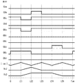
- AC power supply 1 is a waveform schematic diagram which shows the operation state of the area
- AC power supply 1 is a wave form diagram which shows the operation state of the area
- AC power supply 1 is a waveform schematic diagram which shows the operation state of the area
- AC power supply 1 is a wave form diagram which shows the operation state of the area
- AC power supply 1 is a wave form diagram which shows the operation state of the area
- AC power supply 1 is a wave form diagram which shows the operation state of the area
- FIG. 3 is a gate pattern diagram in region 1 of the first embodiment.
- FIG. 4 is a gate pattern diagram in region 3 of the first embodiment.
- AC power supply 1 is a wave form diagram which shows the operation state of the area
- AC power supply 1 is a waveform schematic diagram which shows the operation state of the area
- FIG. 49 is a diagram showing a current path in a sixth period of FIG. 48.
- FIG. 49 is a diagram showing a current path in a seventh period of FIG. 48.
- FIG. 49 is a diagram showing a current path in an eighth period of FIG. 48.
- AC power supply 1 is a wave form diagram which shows the operation state of the area
- FIG. 58 is a diagram showing a current path in a first period of FIG. 57.
- FIG. 58 is a diagram showing a current path in a second period of FIG. 57.
- FIG. 58 is a diagram showing a current path in a third period of FIG. 57.
- FIG. 58 is a diagram showing a current path in a fourth period of FIG. 57.
- AC power supply 1 is a wave form diagram which shows the operation state of the area
- FIG. 63 is a diagram showing a current path in a first period of FIG. 62.
- FIG. 63 is a diagram showing a current path in a second period of FIG. 62.
- FIG. 63 is a diagram showing a current path in a third period of FIG. 62.
- FIG. 63 is a diagram showing a current path in a fourth period of FIG. 62.
- FIG. 63 is a diagram showing a current path in a fifth period of FIG. 62.
- FIG. 63 is a diagram showing a current path in a sixth period of FIG. 62.
- FIG. 63 is a diagram showing a current path in a seventh period of FIG. 62.
- FIG. 63 is a diagram showing a current path in an eighth period of FIG. 62.
- AC power supply 1 is a wave form schematic diagram which shows the operation state of the area
- FIG. 72 is a diagram showing a current path in a first period of FIG. 71.
- FIG. 72 is a diagram showing a current path in a second period of FIG. 71.
- FIG. 72 is a diagram showing a current path in a third period of FIG. 71.
- FIG. 72 is a diagram showing a current path in a fourth period of FIG. 71.
- FIG. 72 is a diagram showing a current path in a fifth period of FIG. 71.
- FIG. 72 is a diagram showing a current path in a sixth period of FIG. 71.
- FIG. 72 is a diagram showing a current path in a first period of FIG. 71.
- FIG. 72 is a diagram showing a current path in a second period of FIG. 71.
- FIG. 72 is a diagram showing a current path in a third period of FIG. 71.
- AC power supply 1 is a wave form schematic diagram which shows the operation state of the area
- FIG. 6 is a configuration diagram of a control unit 100 in a power conversion device according to a second embodiment. It is a block diagram of the feedback duty calculator 120 which comprises the control part 100 of FIG. It is a block diagram of the gate signal calculator 140 which comprises the control part 100 of FIG.
- FIG. 10 is a gate pattern diagram in region 1 of the second embodiment.
- FIG. 10 is a gate pattern diagram in region 3 of the second embodiment. It is a figure which shows the circuit structure of the power converter device by Embodiment 3 of this invention. It is a figure which shows the relationship of each voltage in the pressure
- AC power supply 1 is a waveform schematic diagram which shows the operation state of the area
- FIG. 94 is a diagram showing a current path in a first period of FIG. 93.
- FIG. 94 is a diagram showing a current path in a second period of FIG. 93.
- FIG. 94 is a diagram showing a current path in a third period of FIG. 93.
- FIG. 94 is a diagram showing a current path in a fourth period of FIG. 93.
- AC power supply 1 is a wave form diagram which shows the operation state of the area
- FIG. 100 is a diagram showing a current path in a third period of FIG. 100. It is a figure which shows the electric current path
- AC power supply 12 is a waveform schematic diagram which shows the operation state of the area
- AC power supply 1 is a wave form diagram which shows the operation state of the area
- AC power supply 1 is a wave form diagram which shows the operation state of the area
- FIG. 119 is a diagram showing a current path in a first period of FIG. 119.
- FIG. 119 is a diagram showing a current path in a second period of FIG. 119.
- FIG. 119 is a diagram showing current paths in the third period of FIG. 119.
- FIG. 119 is a diagram showing current paths in the fourth period of FIG. 119.
- FIG. 119 is a diagram showing a current path in a fifth period of FIG. 119.
- FIG. 119 is a diagram showing a current path in a sixth period in FIG. 119.
- AC power supply 1 is a wave form diagram which shows the operation state of the area
- FIG. 127 is a diagram showing a current path in a first period of FIG. 126.
- FIG. 127 is a diagram showing a current path in a second period of FIG. 126.
- FIG. 127 is a diagram showing a current path in a third period of FIG. 126.
- FIG. 127 is a diagram showing a current path in a fourth period of FIG. 126.
- FIG. 10 is a configuration diagram of a control unit 100 in a power conversion device according to a third embodiment. It is a block diagram of the feedback duty calculator 120 which comprises the control part 100 of FIG.
- FIG. 10 is a gate pattern diagram in region 1 of the third embodiment.
- FIG. 10 is a gate pattern diagram in region 3 of the third embodiment. It is a figure which shows the circuit structure of the power converter device by Embodiment 4 of this invention. It is a figure which shows the relationship of each voltage in the pressure
- AC power supply 1 is a wave form diagram which shows the operation state of the area
- AC power supply 1 is a wave form diagram which shows the operation state of the area
- AC power supply 1 is a wave form diagram which shows the operation state of the area
- FIG. 6 is a waveform schematic diagram showing an operation state of the region 3 in the positive half-wave of the AC power supply 1 when the operation mode in the period 0 to t31 is switched from the mode 7 to the mode 8.
- FIG. 7 is a waveform schematic diagram showing an operation state of the region 3 in the positive half-wave of the AC power supply 1 when the operation mode in the period Tsw to t32 is switched from the mode 8 to the mode 7.
- FIG. 6 is a diagram showing a current path in mode 6.
- FIG. 6 When the operation mode of the period 0 to t31 is switched from the mode 7 to the mode 6 and the operation mode of the period Tsw to t32 is switched from the mode 8 to the mode 6, the operation state of the region 3 in the positive half-wave of the AC power supply 1 is changed. It is a waveform schematic diagram shown.
- FIG. 6 is a waveform schematic diagram showing an operation state of the region 3 when the AC power supply 1 is in a positive half-wave when the operation mode in the period 0 to t31 is switched from the mode 7 to the mode 9;
- FIG. 10 is a waveform schematic diagram showing an operation state of the region 3 in the positive half-wave of the AC power supply 1 when the operation mode in the period t31 to Tsw is switched from the mode 2 to the mode 9.
- FIG. 10 is a waveform schematic diagram showing an operation state of the region 3 in the positive half-wave of the AC power supply 1 when the operation mode in the period Tsw to t32 is switched from the mode 8 to the mode 9;
- FIG. 10 is a waveform schematic diagram showing an operation state of the region 3 in the positive half-wave of the AC power supply 1 when the operation mode in the period t32 to 2Tsw is switched from the mode 1 to the mode 9.
- FIG. 10 is a waveform schematic diagram showing an operation state of the region 3 in the negative half-wave of the AC power supply 1 when the operation mode in the period 0 to t31 is switched from the mode 7 to the mode 8.
- FIG. 10 is a waveform schematic diagram showing an operation state of the region 3 in the negative half-wave of the AC power supply 1 when the operation mode in the period Tsw to t32 is switched from the mode 8 to the mode 7.
- FIG. 6 is a diagram showing a current path in mode 6.
- FIG. 6 When the operation mode of the period 0 to t31 is switched from the mode 7 to the mode 6 and the operation mode of the period Tsw to t32 is switched from the mode 8 to the mode 6, the operation state of the region 3 in the negative half wave of the AC power supply 1 is changed. It is a waveform schematic diagram shown.
- FIG. 7 is a waveform schematic diagram showing an operation state of the region 3 in the negative half-wave of the AC power supply 1 when the operation mode in the period 0 to t31 is switched from the mode 7 to the mode 9;
- FIG. 10 is a waveform schematic diagram showing an operation state of the region 3 in the negative half wave of the AC power supply 1 when the operation mode in the period t31 to Tsw is switched from the mode 2 to the mode 9.
- FIG. 10 is a waveform schematic diagram showing an operation state of the region 3 in the negative half-wave of the AC power supply 1 when the operation mode in the period Tsw to t32 is switched from the mode 8 to the mode 9.
- FIG. 10 is a waveform schematic diagram showing an operation state of the region 3 in the negative half wave of the AC power supply 1 when the operation mode in the period t32 to 2Tsw is switched from the mode 1 to the mode 9.
- It is a block diagram of the control part 100 in the power converter device by Embodiment 4.
- FIG. 4 It is a block diagram of the control part 100 in the power converter device by Embodiment 4.
- FIG. 167 is a configuration diagram of a region 3 gate signal calculator 143 and a region 3 DC capacitor voltage controller 182 that constitute the control unit 100 of FIG. 167 is a configuration diagram of a region 1 / basin region 2 DC capacitor voltage controller 181, a region 1 gate signal computing unit 141, and a region 2 gate signal computing unit 142 constituting the control unit 100 of FIG. 167.
- FIG. Embodiment 1 of the present invention will be described below.
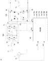
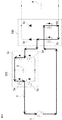
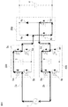
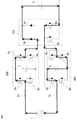
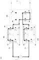
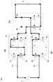
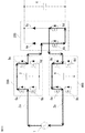
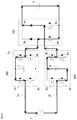
- 1 is a circuit configuration diagram of a power conversion device according to Embodiment 1 of the present invention.
- the power conversion device includes a main circuit and a control unit 100 for converting AC voltage and AC power of a single-phase AC power source 1 into DC voltage and DC power and outputting the DC voltage to the smoothing capacitor 4. .
- the main circuit includes a single-phase inverter 300, a single-phase converter 200, and a reactor 2 that are connected in series between the AC power source 1 and the smoothing capacitor 4.
- the single-phase inverter 300 includes a DC capacitor 3, a first leg and a third switch element 5 c that are connected in parallel to the DC capacitor 3 and are composed of a series body of a first switch element 5 a and a second switch element 5 b. And a second leg formed in series with the fourth switch element 5d.
- the single-phase converter 200 is connected in parallel with each other by a third leg composed of a series body of a fifth switch element 6b and a first diode 6a and a sixth body composed of a series body of a sixth switch element 6d and a second diode 6c. It has four legs.
- connection point between the first switch element 5a and the second switch element 5b of the single-phase inverter 300 that is, one of the inverter AC terminals of the single-phase inverter 300, the middle point of the first leg and the AC power supply 1 A reactor 2 is connected between one end.
- the midpoint of the second leg which is the other inverter AC terminal 5f of the single-phase inverter 300, is connected to the midpoint of the third leg, which is the converter AC terminal 6e of the single-phase converter 200.
- the middle point of the fourth leg which is the other 6f of the converter AC terminal of the single-phase converter 200, is connected to the other end of the AC power source 1. Further, the upper and lower ends of the third leg and the fourth leg are respectively connected to the smoothing capacitor 4 as converter DC terminals 6g and 6h.
- the control unit 100 includes a voltage vac of the AC power supply 1 detected by the AC voltage detection unit 10, a current iac of the AC power supply 1 detected by the AC current detection unit 11, and a DC detected by the DC capacitor voltage detection unit 12.
- the voltage Vc2 of the capacitor 3 and the voltage Vc1 of the smoothing capacitor 4 detected by the DC voltage detector 13 are input, and a control operation described in detail below is executed, whereby the switching elements 5a to 5d of the single-phase inverter 300 are performed.
- Gate signals G5a to G5d for switching driving and gate signals G6b and G6d for switching driving the switching elements 6b and 6d of the single-phase converter 200 are output.
- a load (not shown) is connected to the smoothing capacitor 4 in parallel.
- the load may be connected directly to a voltage source such as a resistor or a battery, or may be connected to a voltage source such as a resistor or a battery via a power converter such as a DC-DC converter or a DC-AC inverter. Good.
- Each of the switch elements 5a to 5d, 6b, and 6d includes a MOSFET (Metal Oxide Semiconductor Field Effect Transistor) in which a diode is incorporated.
- the diodes 6a and 6c can be formed of MOSFETs.
- these switching elements are semiconductors using compound semiconductors such as IGBTs (Insulated Gate Bipolar Transistors), SiC (Silicon Carbide), and GaN (Gallium Nitride) with a built-in diode between the source and drain. An element may be used.
- Single-phase converter 200 switches the voltage level between converter AC terminals 6e and 6f to Vc1, ⁇ Vc1, which is the positive / negative value of the voltage of smoothing capacitor 4, or zero voltage by the switching operation of switch elements 6b and 6d.
- Single-phase inverter 300 switches the voltage level between inverter AC terminals 5e and 5f to Vc2, -Vc2 which is the positive / negative value of the voltage of DC capacitor 3, or zero voltage by the switching operation of switch elements 5a to 5d.
- the direction of the output voltage of single phase converter 200 and single phase inverter 300 is determined by the relationship among voltage vac of AC power supply 1, voltage Vc1 of smoothing capacitor 4, and voltage Vc2 of DC capacitor 3.
- the voltage Vc2 of the DC capacitor 3 is smaller than the voltage Vc1 of the smoothing capacitor 4.
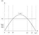
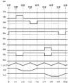
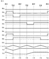
- FIG. 2 shows a voltage relationship when the voltage Vc1 of the smoothing capacitor 4 is larger than the absolute value
- this operation is referred to as a boost operation mode.
- FIG. 3 shows the voltage relationship when the voltage Vc1 of the smoothing capacitor 4 is smaller than the absolute value
- this operation is referred to as a step-down operation mode.
- Tg indicates the cycle of the AC power source 1
- Tg / 2 indicates the half cycle of the AC power source 1.
- region of ⁇ 1 ⁇ t ⁇ ⁇ 2 in FIG. 2 and the region of ⁇ 1 ⁇ t ⁇ 1 and ⁇ 2 ⁇ t ⁇ ⁇ 2 in FIG. 3 are regions where Vc2 ⁇
- region of ⁇ 1 ⁇ t ⁇ ⁇ 2 is a region where Vc1 ⁇
- regions 1 and 2 are referred to as region A, and region 3 is referred to as region B.
- the driving method since the current path is different between the positive half wave and the negative half wave of the AC power supply 1, first, the driving method (gate pattern) and current path in the positive half wave regions 1 to 3, The driving method and current path in the negative half wave will be described.
- the inductance of reactor 2 is defined as L.
- the switching cycle of single-phase inverter 300 and the switching cycle of single-phase converter 200 are equally set to Tsw.
- FIG. 4 is a schematic operation diagram showing an operating state during one switching cycle Tsw in the positive half-wave of the AC power source 1 and in the region 1.
- one switching cycle Tsw is divided into two pairs of periods in which the current
- Drive with high frequency PWM The increase / decrease in the current of the AC power supply 1 may be decreased in the first half and increased in the second half.
- the current increase period and the current decrease period may be a pair of periods. The same applies to the following cases.
- the switch elements 5c and 6b are in an on state, the AC power supply 1 is short-circuited by the single-phase converter 200, and the current
- the current at this time flows through the path shown in FIG.
- the path is AC power source 1 ⁇ reactor 2 ⁇ switch element 5a ⁇ switch element 5c ⁇ switch element 6b ⁇ switch element 6d ⁇ AC power source 1.
- the voltage Vc2 is a constant voltage.
- the current change amount ⁇ iac11 during this period is expressed by the following equation (1) and takes a positive value.
- ⁇ iac11 (
- ⁇ iac12 ((
- the switch elements 5c and 6b are in the on state, the AC power supply 1 is short-circuited by the single-phase converter 200, and the current
- the current at this time flows through the path shown in FIG.
- the path is AC power source 1 ⁇ reactor 2 ⁇ switch element 5a ⁇ switch element 5c ⁇ switch element 6b ⁇ switch element 6d ⁇ AC power source 1.
- the voltage Vc2 is a constant voltage.
- the current change amount ⁇ iac13 during this period is expressed by the following formula (3) and takes a positive value.
- ⁇ iac13 (
- the switch element 6b In the fourth period of t13 ⁇ t ⁇ Tsw, the switch element 6b is in an ON state, and the DC capacitor 3 is charged by the AC power supply 1, so the current
- the current at this time flows through the path shown in FIG. The path is AC power source 1 ⁇ reactor 2 ⁇ switch element 5a ⁇ DC capacitor 3 ⁇ switch element 5d ⁇ switch element 6b ⁇ switch element 6d ⁇ AC power source 1.
- a current flows through the DC capacitor 3 in the charging direction, and the voltage Vc2 increases.
- the current change amount ⁇ iac14 during this period is expressed by the following formula (4), and is a negative value.
- ⁇ iac14 ((
- the theoretical duty D11 as the theoretical duty 1 which is the ratio of the period from 0 to t11 with respect to the period from 0 to t12, is the period from t11 to t12 in Expression (5).
- the theoretical duty D12 as the theoretical duty 2 that is the ratio of is expressed by the equation (6).
- D11 (Vc1-
- D12 1-D11 (6)
- the duty D13 which is the ratio of the period from t12 to t13 with respect to the period from t12 to Tsw
- the duty D14 which is the ratio of the period from t13 to Tsw
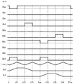
- FIG. 9 shows a schematic diagram of the operation of the AC power supply 1 in the positive half-wave and in the region 2 during one switching cycle Tsw.
- one switching cycle Tsw is divided into four periods and driven by high frequency PWM.
- the switch element 6b In the first period of 0 ⁇ t ⁇ t21, the switch element 6b is on, and the current
- the current at this time flows through the path shown in FIG. The path is AC power source 1 ⁇ reactor 2 ⁇ switch element 5a ⁇ DC capacitor 3 ⁇ switch element 5d ⁇ switch element 6b ⁇ switch element 6d ⁇ AC power source 1.
- the voltage Vc2 increases.
- the current change amount ⁇ iac21 during this period is expressed by the following equation (9) and is a positive value.
- ⁇ iac21 ((
- the switch element 5c In the second period of t21 ⁇ t ⁇ t22, the switch element 5c is in the on state, and the current
- the current at this time flows through the path shown in FIG.
- the path is AC power source 1 ⁇ reactor 2 ⁇ switch element 5a ⁇ switch element 5c ⁇ diode 6a ⁇ smoothing capacitor 4 ⁇ switch element 6d ⁇ AC power source 1.
- the voltage Vc2 is a constant voltage.
- the current change amount ⁇ iac22 during this period is expressed by the following formula (10) and takes a negative value.
- ⁇ iac22 ((
- ⁇ iac23 ((
- ⁇ iac24 ((
- Duty D21 which is the ratio of the period from 0 to t21 with respect to the period from 0 to t22, is a theoretical ratio that is the ratio of the period from t21 to t22 in Expression (13).
- Duty D22 is expressed by equation (14).
- FIG. 14 shows a schematic operation diagram of the AC power supply 1 in the positive half-wave and region 3 during one switching cycle Tsw.
- one switching cycle Tsw is divided into two periods, and driving is performed by high-frequency PWM.
- the switch elements 5b and 5c are on, and the current
- the current flows through the path shown in FIG.
- the path is AC power source 1 ⁇ reactor 2 ⁇ switch element 5b ⁇ DC capacitor 3 ⁇ switch element 5c ⁇ diode 6a ⁇ smoothing capacitor 4 ⁇ switch element 6d ⁇ AC power source 1.
- the voltage Vc2 decreases.
- the current change amount ⁇ iac31 during this period is expressed by the following equation (17) and is a positive value.
- ⁇ iac31 ((
- ⁇ iac32 ((
- FIG. 17 shows an operation schematic diagram in the negative half wave of the AC power supply 1 and in the region 1 during one switching cycle Tsw.
- One switching cycle Tsw is divided into four periods and driven by high frequency PWM.
- the switch elements 5a and 6d are on, and the current
- the current at this time flows through the path shown in FIG.
- the path is AC power source 1 ⁇ switch element 6d ⁇ switch element 6b ⁇ switch element 5c ⁇ switch element 5a ⁇ reactor ⁇ AC power source 1.
- the voltage Vc2 is a constant voltage.
- the current change amount ⁇ iac11 during this time is expressed by the following equation (21) and takes a positive value.
- ⁇ iac11 (
- the switch elements 5a and 5d are on, and the current
- the current at this time flows through the path shown in FIG.
- the path is AC power source 1 ⁇ diode 6c ⁇ smoothing capacitor 4 ⁇ switch element 6b ⁇ switch element 5d ⁇ DC capacitor 3 ⁇ switch element 5a ⁇ reactor 2.
- a current flows through the DC capacitor 3 in the discharging direction, and the voltage Vc2 decreases.
- the current change amount ⁇ iac12 during this period is expressed by the following equation (22) and takes a negative value.
- ⁇ iac12 ((
- ⁇ iac13 (
- the switch element 6d In the fourth period of t13 ⁇ t ⁇ Tsw, the switch element 6d is on, and the current
- the current at this time flows through the path shown in FIG.
- the path is AC power source 1 ⁇ switch element 6d ⁇ switch element 6b ⁇ switch element 5c ⁇ DC capacitor 3 ⁇ switch element 5b ⁇ reactor 2 ⁇ AC power source 1.
- a current flows through the DC capacitor 3 in the charging direction, and the voltage Vc2 increases.
- the current change amount ⁇ iac14 during this period is expressed by the following equation (24) and takes a negative value.
- ⁇ iac14 ((
- Duty D11 which is the ratio of the period from 0 to t11 with respect to the period from 0 to t12, is a theoretical ratio that is the ratio of the period from t11 to t12 in Expression (25).
- Duty D12 is expressed by equation (26).
- D11 (Vc1-
- D12 1-D11 Formula (26)
- FIG. 22 shows a schematic diagram of an operation during one switching cycle Tsw in the negative half-wave of the AC power source 1 and in the region 2.
- One switching cycle Tsw is divided into four periods and driven by high frequency PWM.
- the switch element 6d In the first period of 0 ⁇ t ⁇ t21, the switch element 6d is in the on state, and the current
- the current at this time flows through the path shown in FIG. The path is AC power source 1 ⁇ switch element 6d ⁇ switch element 6b ⁇ switch element 5c ⁇ DC capacitor 3 ⁇ switch element 5b ⁇ reactor 2 ⁇ AC power source 1.
- the voltage Vc2 increases.
- the current change amount ⁇ iac21 during this period is expressed by the following equation (29) and is a positive value.
- ⁇ iac21 ((
- ⁇ iac22 ((
- ⁇ iac23 ((
- ⁇ iac24 ((
- Duty D21 which is the ratio of the period from 0 to t21 with respect to the period from 0 to t22, is the ratio of the period from t21 to t22 in Expression (33).
- Duty D22 is expressed by equation (34).
- FIG. 27 shows a schematic diagram of an operation during one switching cycle Tsw in the negative half-wave of the AC power source 1 and in the region 3.
- One switching cycle Tsw is divided into two periods and driven by high frequency PWM.
- the switch elements 5a and 5d are on, and the current
- the current at this time flows through the path shown in FIG.
- the path is AC power source 1 ⁇ diode 6c ⁇ smoothing capacitor 4 ⁇ switch element 6b ⁇ switch element 5d ⁇ DC capacitor 3 ⁇ switch element 5a ⁇ reactor 2 ⁇ AC power source 1.
- the voltage Vc2 decreases.
- the current change amount ⁇ iac31 during this period is expressed by the following equation (37) and takes a positive value.
- ⁇ iac31 ((
- ⁇ iac32 ((
- D31 (Vc1 + Vc2-
- D32 1 ⁇ D31 (40)
- D11 to D14 are the same calculation formula.
- ⁇ D24 is the same calculation formula.
- the positive half-wave theoretical duties D31 and D32 represented by the equations (19) and (20) and the negative half-wave theoretical duty represented by the equations (39) and (40) are used.
- D31 and D32 are the same calculation formula.
- the DC capacitor 3 performs charging and discharging operations in the above-described pair of periods within one switching cycle Tsw of the single-phase inverter 300, and the charging amount and discharging amount thereof. And become equal.
- the switching frequency of the single-phase inverter 300 is typically 10 kHz or more with respect to the frequency 50 to 60 Hz of the AC power supply 1, the DC capacitor 3 has no relation to the long cycle of the AC power supply 1. Since the charge / discharge operation is completed within one short switching cycle of the single-phase inverter 300, the charge / discharge amount itself is reduced, and the capacity required for the DC capacitor 3 to suppress the ripple voltage can be greatly reduced. I can do it. Further, as can be seen from FIGS. 4, 9, and the like, in regions 1 and 2, the applied voltage frequency of the reactor 2 is twice the switching frequency (1 / Tsw) of the single-phase inverter 300, and the reactor 2 can be downsized. To do.
- control unit 100 responsible for generating a gate signal for switching driving each switch element
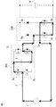
- control unit 100 includes a theoretical duty calculator 110, a feedback duty calculator 120, an adder / subtractor 130, a gate signal calculator 140, an operation region determiner 150, and a gate signal selector 160. .
- the theoretical duty calculator 110 includes a region 1 theoretical duty calculator 111, a region 2 theoretical duty calculator 112, and a region 3 theoretical duty calculator 113, and calculates the theoretical duty using the theoretical formulas of the regions 1 to 3. .
- Area 1 theoretical duty calculator 111 calculates theoretical duties D11 to D14 according to equations (5) to (8) or equations (25) to (28).
- the region 2 theoretical duty calculator 112 calculates the theoretical duties D21 to D24 according to the equations (13) to (16) or the equations (33) to (36).
- the area 3 theoretical duty calculator 113 calculates the theoretical duties D31 and D32 according to the equations (19), (20), (39), and (40).
- Each theoretical duty is the voltage vac of the AC power source 1 or the ideal voltage value vac * of the AC power source 1 that is a detection value of the AC voltage detection unit 10, the voltage Vc2 of the DC capacitor 3 that is a detection value of the DC capacitor voltage detection unit 12, or It is calculated based on the voltage command value vc2 * of the DC capacitor 3, the voltage Vc1 of the smoothing capacitor 4 which is the detected value of the DC voltage detection unit 13, or the voltage command value Vc1 * of the smoothing capacitor 4.
- FIG. 30 shows a case where the calculation is performed based on the detection value of each voltage detection unit.
- the feedback duty calculator 120 has the configuration shown in FIG. After calculating the deviation between the DC voltage detection value Vc1 of the smoothing capacitor 4 and the command value Vc1 * by a subtractor, PI control is performed by the PI controller, and a limiter is provided to calculate the current amplitude command value ⁇ 2Iac * of the AC power source 1. To do. On the other hand, from the AC voltage detection value vac of the AC power supply 1, a phase ⁇ synchronized with vac and the phase is calculated by PLL (Phase Locked Loop). Thereafter, the phase ⁇ is a sine wave, and the current amplitude command value ⁇ 2Iac * of the AC power source 1 is multiplied by the AC current command value iac * of the AC power source 1 to be calculated.
- PLL Phase Locked Loop
- the deviation between the AC current command value iac * and the AC current detection value iac is PI-controlled by the PI controller, divided by the DC capacitor Vc2, and then provided with a limiter to obtain the feedback duty DFB.
- the adder / subtractor 130 adds / subtracts the feedback duty DFB to the calculation result of the theoretical duty calculator 110.
- the DFB is added to the D11, D13, D21, D23, D31 by the adders 131, 133, 135, and D12, D14, D22,
- the DFB is subtracted from D24 and D32 by the subtracters 132, 134, and 136.
- FIG. 32 shows a configuration diagram of the gate signal calculator 140.
- the gate signal computing unit 140 includes a region 1 gate signal computing unit 141, a region 2 gate signal computing unit 142, and a region 3 gate signal computing unit 143, and computes a gate signal for each switching period from the input duty.
- the region 1 gate signal computing unit 141 is composed of four comparators and a carrier signal cararea1 and compares the input signals D11 + DFB, D12-DFB, D13 + DFB, D14-DFB and the carrier signal cararea1 with each comparator, and the first period. , The second period signal G12, the third period signal G13, and the fourth period signal G14.
- the region 2 gate signal calculator 142 is composed of two comparators and a carrier signal cararea2, compares the input signals D21 + DFB, D22-DFB, D23 + DFB, D24-DFB and the carrier signal cararea2 with each comparator, and performs the first period.
- the region 3 gate signal computing unit 143 is composed of two comparators and a carrier signal carrier3, and compares the input signals D31 + DFB, D32 ⁇ DFB and the carrier signal carrier3 with each comparator, and compares the signal G31 in the first period and the first signal G31.
- the signal G32 of the period 2 is generated.
- Each signal is input to the gate signal selector 160 and distributed to the gate signal of each switch element.
- the absolute value calculator 170 calculates an absolute value
- the operation region determination unit 150 compares the magnitude relationship between the absolute value
- the gate signal selector 160 assigns the output of the gate signal calculator 140 to each switch element using the region signal sigarea which is the output of the operation region determiner 150.
- the region 1 and the region 2 perform control by dividing one switching cycle into four periods
- the region 3 performs control by dividing one switching cycle into two periods.
- a gate pattern diagram in the positive half-wave region 1 is shown in FIG.
- a gate pattern diagram in the positive half-wave region 3 is shown in FIG.
- one switching cycle and one-half switching cycle are made constant, and the on-time ratio between them is controlled. That is, in FIG. 33, times 0, t12, and Tsw are fixed, and the control unit 100 controls t11 and t13. Note that t11 and t13 correspond to the timing for determining the boundary between the current increase period and the current decrease period for the current of the AC power supply 1, and this is referred to as a control axis in the claims of the present application. The same applies to the subsequent t31 and the like.
- the switching period is set to be constant, and the on-time ratio during that period is controlled.
- the reference switching cycle is constant, and PWM (Pulse Width Modulation) control can be used.
- One switching period is made constant, and the on-time ratio during that period is controlled. That is, in FIG. 34, time 0 and Tsw are fixed, and t31 is controlled.
- the control unit 100 in the power conversion device according to Embodiment 1 of the present invention sets one switching cycle Tsw of the single-phase inverter 300 to be the same as one switching cycle Tsw of the single-phase converter 200, and the current of the AC power supply 1
- the pair of periods that increase in the first half and decrease in the second half are divided into even periods having one or two pairs, and the increase in the first half of the current of the AC power supply 1 and the decrease in the second half are equal in the pair of periods
- the switching element of the single-phase inverter 300 and the switching element of the single-phase converter 200 based on the theoretical duty 2
- the gate signal calculator 140 that calculates the moving gate signal
- the DC capacitor 3 completes the charging / discharging operation within one short switching period of the single-phase inverter 300 regardless of the long period of the AC power supply 1, the charging / discharging amount itself is reduced. Since the ripple voltage is suppressed, the capacity required for the DC capacitor 3 can be greatly reduced, and the apparatus can be downsized.
- control unit 100 generates a voltage controller that generates an AC current command value based on a deviation between the DC voltage command value and the DC voltage detection value, and a feedback duty based on a deviation between the AC current command value and the AC current detection value. Since the feedback duty calculator 120 for calculating is provided, and the gate signal calculator 140 adds the feedback duty to the theoretical duty 1 and subtracts it from the theoretical duty 2, the gate signal is calculated. Constant voltage control that keeps the voltage of the capacitor 4 at a desired DC voltage command value becomes possible.
- control unit 100 determines the number of divisions in one switching period of the single-phase inverter 300 depending on the magnitude relationship among the voltage vac of the AC power supply 1, the voltage Vc1 of the smoothing capacitor 4, and the voltage Vc2 of the DC capacitor 3. Since it is set according to 1, 2, and 3, it is possible to perform switching control of each switch element by an appropriate gate pattern adapted to these voltage relationships.
- the control part 100 controlled each switch element so that the switching timing of the single phase inverter 300 and the single phase converter 200 may mutually shift, the applied voltage frequency of the reactor 2 is changed to the single phase inverter 300 or the single phase converter. It becomes possible to make the frequency higher than the switching frequency of 200. As a result, it is possible to reduce the VT product that is the voltage-time product of the reactor 2 with a general configuration ratio, and the necessary inductance value can be reduced in principle. In general, in the reactor 2, the inductance value is reduced by reducing the core size or reducing the number of turns. As a result, the reactor 2 is reduced in size.
- the upper arm of single-phase converter 200 is configured with diodes 6a and 6c, but may be configured with a switch element (alternative switch element) as with the lower arm. .
- the so-called synchronous rectification operation can be performed by turning on the switch element.
- the switching elements 5a to 5d of the single-phase inverter 300 and the switching elements 6b and 6d of the single-phase converter 200 the synchronous rectification operation is performed by turning on the switching elements when the diodes connected in parallel are conducting. It can be performed.
- the switching period Tsw of each region may be a constant value or may be an individual value.
- the switching cycle of the region 1 and the region 2 may be constant, and the switching cycle of the region 3 may be set to half of the region 1 and the region 2.
- the applied voltage frequency of the reactor 2 becomes constant in all the regions.
- PFM Pulse Frequency Modulation
- the reactor 2 is provided with the reactor 2 on the P side line of the AC power source 1, it may be connected only to the N side line or may be connected to both sides of the PN. Further, it may be connected between the single-phase inverter 300 and the single-phase converter 200. Similarly, although the single-phase inverter 300 is provided on the P-side line of the AC power supply 1, it may be configured on the N-side line.
- a diode bridge 500 that is a rectifier circuit may be used.
- both ends of the AC power supply 1 are connected to the AC terminal of the diode bridge 500, and the reactor 2, the single-phase inverter 300, and the AC terminals of the single-phase converter 200 are connected in series to the P-side DC output terminal.
- the N-side DC output terminal of the diode bridge 500 is connected to the source terminal of the switch element 6 b of the single-phase converter 200 and one terminal of the smoothing capacitor 4.
- the other terminal of smoothing capacitor 4 is connected to the cathode terminal of diode 6 a of single-phase converter 200.
- 35 can be driven using only the positive half-wave control of the configuration shown in FIG. 1, and the obtained effect is the same as in the case of FIG.
- the reactor 2 may be connected to at least one of the PN lines between the AC power supply 1 and the diode bridge 500, or may be connected between the single-phase inverter 300 and the single-phase converter 200. . Further, at least one current of the PN line between the AC power supply 1 and the diode bridge 500 may be detected. Further, the AC power supply 1 and the diode bridge 500 can be regarded as a DC power supply, and a DC / DC converter capable of stepping up and down the DC voltage of the smoothing capacitor 4 with respect to the DC power supply voltage can be obtained.
- the feedback duty calculator 120 shown in FIG. 31 does not perform Vc1 constant control.
- only current control may be performed with a predetermined current amplitude command value ⁇ 2Iac * of the AC power supply 1. In this case, high power factor operation can be controlled.
- the AC power supply can be a three-phase power supply.
- the single-phase inverter shown in FIG. 1 is provided for three phases, and one of the inverter AC terminals of the single-phase inverter of each phase is connected to each phase terminal of the three-phase power source via the reactor of each phase.
- a leg composed of a series of switch elements and diodes is provided for three phases, and the converter AC terminal of each phase corresponding to the midpoint of each phase leg is connected to the other of the inverter AC terminals of the single-phase inverter of each phase. It consists of a three-phase converter in which converter DC terminals corresponding to the upper and lower ends of the phase leg are connected to a smoothing capacitor.
- the power can be reduced between the three-phase AC voltage and the DC voltage by reducing the capacity of the DC capacitor of each phase inverter.
- a power converter that performs conversion can be provided.
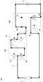
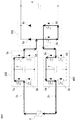
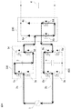
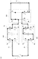
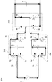
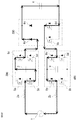
- FIG. 36 is a circuit configuration diagram of a power conversion device according to Embodiment 2 of the present invention.
- the power conversion device includes a main circuit for converting the AC voltage and AC power of the AC power source 1 into DC voltage and DC power and outputting the DC voltage to the smoothing capacitor 4 and the control unit 100.
- FIG. 36 demonstrates centering on a different part from the structure shown in FIG. 1 of previous Embodiment 1.
- the main circuit includes a single-phase inverter 400 connected to the lower end of the AC power supply 1 in addition to the single-phase inverter 300 whose inverter AC terminal 5e is connected to the upper end of the AC power supply 1 via the reactor 2a.
- Single-phase inverter 400 has the same configuration as single-phase inverter 300, and includes two legs consisting of a series body of DC capacitor 9 and a pair of switch elements 8a, 8b and 8c, 8d, which corresponds to the midpoint of one leg
- the inverter AC terminal 8e to be connected is connected to the lower end of the AC power source 1 through the reactor 2b.
- the inverter AC terminal 5f of the single-phase inverter 300 is the converter AC terminal 6e of the single-phase converter 200
- the inverter AC terminal 8f corresponding to the midpoint of the other leg of the single-phase inverter 400 is the converter AC terminal of the single-phase converter 200.
- Each is connected to 6f.
- the control unit 100 adds the DC capacitor 9 detected by the DC capacitor voltage detection unit 14.
- Voltage Vc3 is input, in addition to gate signals G5a to G5d for switching driving the switching elements 5a to 5d of the single phase inverter 300 and gate signals G6b and G6d for switching driving the switching elements 6b and 6d of the single phase converter 200, Gate signals G8a to G8d for switching the switching elements 8a to 8d of the single-phase inverter 400 are output.
- the single-phase inverter 400 changes the voltage level between the inverter AC terminals 8e and 8f by the switching operation of the switch elements 8a to 8d to Vc3, -Vc3, which is the positive / negative value of the voltage of the DC capacitor 9, or Switch to zero voltage.
- the direction of the output voltage of single-phase converter 200, single-phase inverter 300 and single-phase inverter 400 is the relationship among voltage vac of AC power supply 1, voltage Vc1 of smoothing capacitor 4, voltage Vc2 of DC capacitor 3, and voltage Vc3 of DC capacitor 9. Determined by.
- the voltage Vc2 of the DC capacitor 3 and the voltage Vc3 of the DC capacitor 9 are smaller than the voltage Vc1 of the smoothing capacitor 4.
- FIG. 37 and FIG. 38 are obtained by rewriting FIG. 2 and FIG. 3 in the first embodiment by applying them to this second embodiment. Then, in the same manner as described above, in FIG. 37 and FIG. 38, in the region where the phase t is 0 ⁇ t ⁇ 1 and ⁇ 2 ⁇ t ⁇ Tg / 2, the relationship
- the region of ⁇ 1 ⁇ t ⁇ ⁇ 2 in FIG. 37 and the region of ⁇ 1 ⁇ t ⁇ 1 and ⁇ 2 ⁇ t ⁇ ⁇ 2 in FIG. 38 are regions where Vsub ⁇
- the driving method since the current path is different between the positive half wave and the negative half wave of the AC power supply 1, first, the driving method (gate pattern) and current path in the positive half wave regions 1 to 3, The driving method and current path in the negative half wave will be described.
- the total inductance of reactors 2a and 2b is defined as L.
- the switching period 2Tsw of the single-phase inverters 300 and 400 is set to twice the switching period Tsw of the single-phase converter 200.
- FIG. 39 is an operation schematic diagram showing an operation state during the positive half-wave of the AC power supply 1 and in the region 1 during the period of one switching cycle 2Tsw of the inverter (two switching cycles of the converter).
- the single-phase inverter 300 and the single-phase converter 200 operate in the first half switching cycle Tsw
- the single-phase inverter 400 and the single-phase converter 200 operate in the second switching cycle Tsw.
- the switching cycle Tsw is divided into four periods and driven by high frequency PWM.
- the switch elements 5c, 6b, and 8a are on, and the current
- the current at this time flows through the path shown in FIG.
- the path is AC power source 1 ⁇ reactor 2a ⁇ switch element 5a ⁇ switch element 5c ⁇ switch element 6b ⁇ switch element 6d ⁇ switch element 8c ⁇ switch element 8a ⁇ reactor 2b ⁇ AC power source 1.
- the voltages Vc2 and Vc3 are constant voltages.
- the current change amount ⁇ iac11 during this period is expressed by the following equation (41) and takes a positive value.
- ⁇ iac11 (
- the switch elements 5b, 5c, and 8a are on, and the current
- the current at this time flows through the path shown in FIG.
- the path is AC power source 1 ⁇ reactor 2a ⁇ switch element 5b ⁇ DC capacitor 3 ⁇ switch element 5c ⁇ diode 6a ⁇ smoothing capacitor 4 ⁇ switch element 6d ⁇ switch element 8c ⁇ switch element 8a ⁇ reactor 2b ⁇ AC power source 1.
- a current flows in the DC capacitor 3 in the discharging direction, the voltage Vc2 decreases, and no current flows in the DC capacitor 9, so the voltage Vc3 becomes a constant voltage.
- the current change amount ⁇ iac12 during this period is expressed by the following equation (42) and takes a negative value.
- ⁇ iac12 ((
- the switch elements 5c, 6b, and 8a are on, and the current
- the current at this time flows through the path shown in FIG.
- the path is AC power source 1 ⁇ reactor 2a ⁇ switch element 5a ⁇ switch element 5c ⁇ switch element 6b ⁇ switch element 6d ⁇ switch element 8c ⁇ switch element 8a ⁇ reactor 2b ⁇ AC power source 1.
- the voltages Vc2 and Vc3 are constant voltages.
- the current change amount ⁇ iac13 during this period is expressed by the following equation (43) and is a positive value.
- ⁇ iac13 (
- the switch elements 6b and 8a are on, and the current
- the current at this time flows through the path shown in FIG.
- the path is AC power source 1 ⁇ reactor 2a ⁇ switch element 5a ⁇ DC capacitor 3 ⁇ switch element 5d ⁇ switch element 6b ⁇ switch element 6d ⁇ switch element 8c ⁇ switch element 8a ⁇ reactor 2b ⁇ AC power source 1.
- a current flows through the DC capacitor 3 in the charging direction, the voltage Vc2 increases, and no current flows through the DC capacitor 9, so the voltage Vc3 becomes a constant voltage.
- the current change amount ⁇ iac14 during this period is expressed by the following formula (44), and is a negative value.
- ⁇ iac14 ((
- the switch elements 5c, 6b, and 8a are on, and the current
- the current at this time flows through the path shown in FIG.
- the path is AC power source 1 ⁇ reactor 2a ⁇ switch element 5a ⁇ switch element 5c ⁇ switch element 6b ⁇ switch element 6d ⁇ switch element 8c ⁇ switch element 8a ⁇ reactor 2b ⁇ AC power source 1.
- the voltages Vc2 and Vc3 are constant voltages.
- the current change amount ⁇ iac15 during this period is expressed by the following equation (45) and takes a positive value.
- ⁇ iac15 (
- the switch elements 5c, 8a, and 8d are in the on state, and the current
- the current at this time flows through the path shown in FIG.
- the path is AC power source 1 ⁇ reactor 2a ⁇ switch element 5a ⁇ switch element 5c ⁇ diode 6a ⁇ smoothing capacitor 4 ⁇ switch element 6d ⁇ switch element 8d ⁇ DC capacitor 9 ⁇ switch element 8a ⁇ reactor 2b ⁇ AC power source 1.
- a current flows through the DC capacitor 9 in the discharge direction, the voltage Vc3 decreases, and no current flows through the DC capacitor 3, so the voltage Vc2 becomes a constant voltage.
- the current change amount ⁇ iac16 during this period is expressed by the following formula (46) and takes a negative value.
- ⁇ iac16 ((
- the switch elements 5c and 6b are on, and the current
- the current at this time flows through the path shown in FIG.
- the path is AC power source 1 ⁇ reactor 2a ⁇ switch element 5a ⁇ switch element 5c ⁇ switch element 6b ⁇ switch element 6d ⁇ switch element 8c ⁇ DC capacitor 9 ⁇ switch element 8b ⁇ reactor 2b ⁇ AC power source 1.
- a current flows in the charging direction in the DC capacitor 9, the voltage Vc3 increases, and no current flows in the DC capacitor 3, so the voltage Vc2 becomes a constant voltage.
- the current change amount ⁇ iac18 during this period is expressed by the following equation (48) and takes a negative value.
- ⁇ iac18 ((
- Duty D11 which is the ratio of the period from 0 to t11 with respect to the period from 0 to t12, is a theoretical ratio that is the ratio of the period from t11 to t12 in Expression (49).
- Duty D12 is expressed by equation (50).
- D11 (Vc1-
- D12 1 ⁇ D11 (50)
- the theoretical duty D13 which is the ratio of the period from t12 to t13 with respect to the period from t12 to Tsw, is the formula (51), and the theoretical duty that is the ratio of the period from t13 to Tsw.
- D14 is represented by Formula (52).
- D15 (Vc1-
- D16 1-D15 (54)
- FIG. 48 shows a schematic diagram of the operation of the AC power source 1 in the positive half-wave and in the region 2 during the switching cycle 2Tsw.
- the single-phase inverter 300 and the single-phase converter 200 operate, and in the latter switching period Tsw, the single-phase inverter 400 and the single-phase converter 200 operate.
- the switching cycle Tsw is divided into four periods and driven by high frequency PWM.
- the switch elements 6b and 8a are on, and the current
- the current at this time flows through the path shown in FIG.
- the path is AC power source 1 ⁇ reactor 2a ⁇ switch element 5a ⁇ DC capacitor 3 ⁇ switch element 5d ⁇ switch element 6b ⁇ switch element 6d ⁇ switch element 8c ⁇ switch element 8a ⁇ reactor 2b ⁇ AC power source 1.
- the voltage Vc2 increases, and no current flows in the DC capacitor 9, so the voltage Vc3 becomes a constant voltage.
- the current change amount ⁇ iac21 during this period is expressed by the following equation (57), and is a positive value.
- ⁇ iac21 ((
- the switch elements 5c and 8a are in the on state, and the current
- the current at this time flows through the path shown in FIG.
- the path is AC power source 1 ⁇ reactor 2a ⁇ switch element 5a ⁇ switch element 5c ⁇ diode 6a ⁇ smoothing capacitor 4 ⁇ switch element 6d ⁇ switch element 8c ⁇ switch element 8a ⁇ reactor 2b ⁇ AC power source 1.
- the voltages Vc2 and Vc3 are constant voltages.
- the current change amount ⁇ iac22 during this period is expressed by the following equation (58) and takes a negative value.
- ⁇ iac22 ((
- the switch elements 5b, 5c, and 8a are on, and the current
- the current at this time flows through the path shown in FIG.
- the path is AC power source 1 ⁇ reactor 2a ⁇ switch element 5b ⁇ DC capacitor 3 ⁇ switch element 5c ⁇ diode 6a ⁇ smoothing capacitor 4 ⁇ switch element 6d ⁇ switch element 8c ⁇ switch element 8a ⁇ reactor 2b ⁇ AC power source 1.
- the voltage Vc2 decreases, and no current flows through the DC capacitor 9, so the voltage Vc3 becomes a constant voltage.
- the current change amount ⁇ iac23 during this time is expressed by the following equation (59), and is a positive value.
- ⁇ iac23 ((
- the switch elements 5c and 8a are in the on state, and the current
- the current at this time flows through the path shown in FIG.
- the path is AC power source 1 ⁇ reactor 2a ⁇ switch element 5a ⁇ switch element 5c ⁇ diode 6a ⁇ smoothing capacitor 4 ⁇ switch element 6d ⁇ switch element 8c ⁇ switch element 8a ⁇ reactor 2b ⁇ AC power source 1.
- the voltages Vc2 and Vc3 are constant voltages.
- the current change amount ⁇ iac24 during this period is expressed by the following equation (60), and is a negative value.
- ⁇ iac24 ((
- the switch elements 5c and 6b are on, and the current
- the current at this time flows through the path shown in FIG.
- the path is AC power source 1 ⁇ reactor 2a ⁇ switch element 5a ⁇ switch element 5c ⁇ switch element 6b ⁇ switch element 6d ⁇ switch element 8c ⁇ DC capacitor 9 ⁇ switch element 8b ⁇ reactor 2b ⁇ AC power source 1.
- the voltage Vc3 increases. Since no current flows in the DC capacitor 3, the voltage Vc2 becomes a constant voltage.
- the current change amount ⁇ iac25 during this period is expressed by the following formula (61), and is a positive value.
- ⁇ iac25 ((
- the switch elements 5c and 8a are in the on state, and the current
- the current at this time flows through the path shown in FIG.
- the path is AC power source 1 ⁇ reactor 2a ⁇ switch element 5a ⁇ switch element 5c ⁇ diode 6a ⁇ smoothing capacitor 4 ⁇ switch element 6d ⁇ switch element 8c ⁇ switch element 8a ⁇ reactor 2b ⁇ AC power source 1.
- the voltages Vc2 and Vc3 are constant voltages.
- the current change amount ⁇ iac26 during this period is expressed by the following equation (62) and takes a negative value.
- ⁇ iac26 ((
- the switch elements 5c, 8a, and 8d are in the on state, and the current
- the current at this time flows through the path shown in FIG.
- the path is AC power source 1 ⁇ reactor 2a ⁇ switch element 5a ⁇ switch element 5c ⁇ diode 6a ⁇ smoothing capacitor 4 ⁇ switch element 6d ⁇ switch element 8d ⁇ DC capacitor 9 ⁇ switch element 8a ⁇ reactor 2b ⁇ AC power source 1.
- the voltage Vc3 decreases, and since no current flows through the DC capacitor 3, the voltage Vc2 becomes a constant voltage.
- the current change amount ⁇ iac27 during this period is expressed by the following equation (63), and is a positive value.
- ⁇ iac27 ((
- the switch elements 5c and 8a are on, and the current
- the current at this time flows through the path shown in FIG.
- the path is AC power source 1 ⁇ reactor 2a ⁇ switch element 5a ⁇ switch element 5c ⁇ diode 6a ⁇ smoothing capacitor 4 ⁇ switch element 6d ⁇ switch element 8c ⁇ switch element 8a ⁇ reactor 2b ⁇ AC power source 1.
- the voltages Vc2 and Vc3 are constant voltages.
- the current change amount ⁇ iac28 during this period is expressed by the following equation (64), and is a negative value.
- ⁇ iac28 ((
- D27 (Vc1-
- D28 1-D27 (72)
- FIG. 57 shows a schematic diagram of the operation of the AC power supply 1 in the positive half-wave and in the region 3 during the switching cycle 2Tsw.
- the single-phase inverter 300 operates, and in the second switching cycle Tsw, the single-phase inverter 400 operates.
- the switching cycle Tsw is divided into two periods and driven by high frequency PWM.
- the switch elements 5b, 5c, and 8a are on, and the current
- the current at this time flows through the path shown in FIG.
- the path is AC power source 1 ⁇ reactor 2a ⁇ switch element 5b ⁇ DC capacitor 3 ⁇ switch element 5c ⁇ diode 6a ⁇ smoothing capacitor 4 ⁇ switch element 6d ⁇ switch element 8c ⁇ switch element 8a ⁇ reactor 2b ⁇ AC power source 1.
- the current change amount ⁇ iac31 during this period is expressed by the following equation (73) and takes a positive value.
- ⁇ iac31 ((
- the switch element 8a In the second period of t31 ⁇ t ⁇ Tsw, the switch element 8a is on, and the current
- the current at this time flows through the path shown in FIG.
- the path is AC power source 1 ⁇ reactor 2a ⁇ switch element 5a ⁇ DC capacitor 3 ⁇ switch element 5d ⁇ diode 6a ⁇ smoothing capacitor 4 ⁇ switch element 6d ⁇ switch element 8c ⁇ switch element 8a ⁇ reactor 2b ⁇ AC power source 1.
- the voltage Vc2 increases. Since no current flows in the DC capacitor 9, the voltage Vc3 becomes a constant voltage.
- the current change amount ⁇ iac32 during this period is expressed by the following formula (74) and takes a negative value.
- ⁇ iac32 ((
- the switch elements 5c, 8a, and 8d are in the on state, and the current
- the current at this time flows through the path shown in FIG.
- the path is AC power source 1 ⁇ reactor 2a ⁇ switch element 5a ⁇ switch element 5c ⁇ diode 6a ⁇ smoothing capacitor 4 ⁇ switch element 6d ⁇ switch element 8d ⁇ DC capacitor 9 ⁇ switch element 8a ⁇ reactor 2b ⁇ AC power source 1.
- the voltage Vc3 decreases. Since no current flows through the DC capacitor 3, the voltage Vc2 becomes a constant voltage.
- the current change amount ⁇ iac33 during this period is expressed by the following formula (75) and takes a positive value.
- ⁇ iac33 ((
- the switch element 5c is on, and the current
- the current at this time flows through the path shown in FIG.
- the path is AC power source 1 ⁇ reactor 2a ⁇ switch element 5a ⁇ switch element 5c ⁇ diode 6a ⁇ smoothing capacitor 4 ⁇ switch element 6d ⁇ switch element 8c ⁇ DC capacitor 9 ⁇ switch element 8b ⁇ reactor 2b ⁇ AC power source 1.
- the voltage Vc3 increases. Since no current flows through the DC capacitor 3, the voltage Vc2 becomes a constant voltage.
- the current change amount ⁇ iac34 during this period is expressed by the following formula (76) and takes a negative value.
- ⁇ iac34 ((
- D31 (Vc1 + Vc2-
- D32 1-D31 (78)
- D33 (Vc1 + Vc3-
- D34 1 ⁇ D33 (80)
- FIG. 62 shows an operation schematic diagram during the switching cycle 2Tsw in the negative half-wave of the AC power source 1 and in the region 1.
- Tsw the single-phase inverter 300 and the single-phase converter 200 operate
- Tsw the single-phase inverter 400 and the single-phase converter 200 operate.
- the switching cycle Tsw is divided into four periods and driven by high frequency PWM.
- the switch elements 5a, 6d, and 8c are on, and the current
- the current at this time flows through the path shown in FIG.
- the path is AC power source 1 ⁇ reactor 2b ⁇ switch element 8a ⁇ switch element 8c ⁇ switch element 6d ⁇ switch element 6b ⁇ switch element 5c ⁇ switch element 5a ⁇ reactor 2a ⁇ AC power source 1.
- the voltages Vc2 and Vc3 are constant voltages.
- the current change amount ⁇ iac11 during this period is expressed by the following equation (81) and takes a positive value.
- ⁇ iac11 (
- the switch elements 5a, 5d, and 8c are on, and the current
- the current at this time flows through the path shown in FIG.
- the path is AC power source 1 ⁇ reactor 2b ⁇ switch element 8a ⁇ switch element 8c ⁇ diode 6c ⁇ smoothing capacitor 4 ⁇ switch element 6b ⁇ switch element 5d ⁇ DC capacitor 3 ⁇ switch element 5a ⁇ reactor 2a ⁇ AC power source 1.
- a current flows in the DC capacitor 3 in the discharging direction, the voltage Vc2 decreases, and no current flows in the DC capacitor 9, so the voltage Vc3 becomes a constant voltage.
- the current change amount ⁇ iac12 during this period is expressed by the following formula (82) and takes a negative value.
- ⁇ iac12 ((
- the switch elements 5a, 6d, and 8c are on, and the current
- the current at this time flows through the path shown in FIG.
- the path is AC power source 1 ⁇ reactor 2b ⁇ switch element 8a ⁇ switch element 8c ⁇ switch element 6d ⁇ switch element 6b ⁇ switch element 5c ⁇ switch element 5a ⁇ reactor 2a ⁇ AC power source 1.
- the voltages Vc2 and Vc3 are constant voltages.
- the current change amount ⁇ iac13 during this period is expressed by the following equation (83) and is a positive value.
- ⁇ iac13 (
- the switch elements 6d and 8c are on, and the current
- the current at this time flows through the path shown in FIG.
- the path is AC power source 1 ⁇ reactor 2b ⁇ switch element 8a ⁇ switch element 8c ⁇ switch element 6d ⁇ switch element 6b ⁇ switch element 5c ⁇ DC capacitor 3 ⁇ switch element 5b ⁇ reactor 2a ⁇ AC power source 1.
- a current flows through the DC capacitor 3 in the charging direction, the voltage Vc2 increases, and no current flows through the DC capacitor 9, so the voltage Vc3 becomes a constant voltage.
- the current change amount ⁇ iac14 during this period is expressed by the following formula (84) and takes a negative value.
- ⁇ iac14 ((
- the switch elements 5a, 6d, and 8c are on, and the current
- the current at this time flows through the path shown in FIG.
- the path is AC power source 1 ⁇ reactor 2b ⁇ switch element 8a ⁇ switch element 8c ⁇ switch element 6d ⁇ switch element 6b ⁇ switch element 5c ⁇ switch element 5a ⁇ reactor 2a ⁇ AC power source 1.
- the voltages Vc2 and Vc3 are constant voltages.
- the current change amount ⁇ iac15 during this period is expressed by the following equation (85) and is a positive value.
- ⁇ iac15 (
- the switch elements 5a, 8b, and 8c are on, and the current
- the current at this time flows through the path shown in FIG.
- the path is AC power source 1 ⁇ reactor 2b ⁇ switch element 8b ⁇ DC capacitor 9 ⁇ switch element 8c ⁇ diode 6c ⁇ smoothing capacitor 4 ⁇ switch element 6b ⁇ switch element 5c ⁇ switch element 5a ⁇ reactor 2a ⁇ AC power source 1.
- a current flows through the DC capacitor 9 in the discharge direction, the voltage Vc3 decreases, and no current flows through the DC capacitor 3, so the voltage Vc2 becomes a constant voltage.
- the current change amount ⁇ iac16 during this period is expressed by the following equation (86) and takes a negative value.
- ⁇ iac16 ((
- the switch elements 5a, 6d, and 8c are on, and the current
- the current at this time flows through the path shown in FIG.
- the path is AC power source 1 ⁇ reactor 2b ⁇ switch element 8a ⁇ switch element 8c ⁇ switch element 6d ⁇ switch element 6b ⁇ switch element 5c ⁇ switch element 5a ⁇ reactor 2a ⁇ AC power source 1.
- the voltages Vc2 and Vc3 are constant voltages.
- the current change amount ⁇ iac17 during this period is expressed by the following equation (87) and is a positive value.
- ⁇ iac17 (
- the switch elements 5a and 6d are on, and the current
- the current at this time flows through the path shown in FIG.
- the path is AC power source 1 ⁇ reactor 2b ⁇ switch element 8a ⁇ DC capacitor 9 ⁇ switch element 8d ⁇ switch element 6d ⁇ switch element 6b ⁇ switch element 5c ⁇ switch element 5a ⁇ reactor 2a ⁇ AC power source 1.
- a current flows in the charging direction in the DC capacitor 9, the voltage Vc3 increases, and no current flows in the DC capacitor 3, so the voltage Vc2 becomes a constant voltage.
- the current change amount ⁇ iac18 during this period is expressed by the following equation (88) and takes a negative value.
- ⁇ iac18 ((
- D11 (Vc1-
- D12 1-D11 (90)
- FIG. 71 shows a schematic operation diagram during the switching cycle 2 Tsw in the negative half-wave of the AC power source 1 and in the region 2.
- the single-phase inverter 300 and the single-phase converter 200 operate, and in the latter switching period Tsw, the single-phase inverter 400 and the single-phase converter 200 operate.
- the switching cycle Tsw is divided into four periods and driven by high frequency PWM.
- the switch elements 6d and 8c are on, and the current
- the current at this time flows through the path shown in FIG.
- the path is AC power source 1 ⁇ reactor 2b ⁇ switch element 8a ⁇ switch element 8c ⁇ switch element 6d ⁇ switch element 6b ⁇ switch element 5c ⁇ DC capacitor 3 ⁇ switch element 5b ⁇ reactor 2a ⁇ AC power source 1.
- the voltage Vc2 increases, and no current flows in the DC capacitor 9, so the voltage Vc3 becomes a constant voltage.
- the current change amount ⁇ iac21 during this period is expressed by the following equation (97) and takes a positive value.
- ⁇ iac21 ((
- ⁇ iac22 ((
- the switch elements 5a, 5d, and 8c are on, and the current
- the current at this time flows through the path shown in FIG.
- the path is AC power source 1 ⁇ reactor 2b ⁇ switch element 8a ⁇ switch element 8c ⁇ diode 6c ⁇ smoothing capacitor 4 ⁇ switch element 6b ⁇ switch element 5d ⁇ DC capacitor 3 ⁇ switch element 5a ⁇ reactor 2a ⁇ AC power source 1.
- the voltage Vc2 decreases, and no current flows through the DC capacitor 9, so the voltage Vc3 becomes a constant voltage.
- the current change amount ⁇ iac23 during this period is expressed by the following equation (99), and is a positive value.
- ⁇ iac23 ((
- the switch elements 5a and 8c are on, and the current
- the current at this time flows through the path shown in FIG.
- the path is AC power source 1 ⁇ reactor 2b ⁇ switch element 8a ⁇ switch element 8c ⁇ diode 6c ⁇ smoothing capacitor 4 ⁇ switch element 6b ⁇ switch element 5c ⁇ switch element 5a ⁇ reactor 2a ⁇ AC power source 1.
- the voltages Vc2 and Vc3 are constant voltages.
- the current change amount ⁇ iac24 during this period is expressed by the following equation (100) and takes a negative value.
- ⁇ iac24 ((
- the switch elements 5a and 6d are in the on state, and the current
- the current at this time flows through the path shown in FIG.
- the path is AC power source 1 ⁇ reactor 2b ⁇ switch element 8a ⁇ DC capacitor 9 ⁇ switch element 8d ⁇ switch element 6d ⁇ switch element 6b ⁇ switch element 5c ⁇ switch element 5a ⁇ reactor 2a ⁇ AC power source 1.
- the voltage Vc3 increases. Since no current flows in the DC capacitor 3, the voltage Vc2 becomes a constant voltage.
- the current change amount ⁇ iac25 during this period is expressed by the following formula (101) and takes a positive value.
- ⁇ iac25 ((
- the switch elements 5a and 8c are on, and the current
- the current at this time flows through the path shown in FIG.
- the path is AC power source 1 ⁇ reactor 2b ⁇ switch element 8a ⁇ switch element 8c ⁇ diode 6c ⁇ smoothing capacitor 4 ⁇ switch element 6b ⁇ switch element 5c ⁇ switch element 5a ⁇ reactor 2a ⁇ AC power source 1.
- the voltages Vc2 and Vc3 are constant voltages.
- the current change amount ⁇ iac26 during this period is expressed by the following formula (102) and takes a negative value.
- ⁇ iac26 ((
- the switch elements 5a, 8b, and 8c are on, and the current
- the current flows through the path shown in FIG.
- the path is AC power source 1 ⁇ reactor 2b ⁇ switch element 8a ⁇ DC capacitor 9 ⁇ switch element 8d ⁇ diode 6c ⁇ smoothing capacitor 4 ⁇ switch element 6b ⁇ switch element 5c ⁇ switch element 5a ⁇ reactor 2a ⁇ AC power source 1.
- the voltage Vc3 decreases, and since no current flows through the DC capacitor 3, the voltage Vc2 becomes a constant voltage.
- the current change amount ⁇ iac27 during this period is expressed by the following equation (103), and is a positive value.
- ⁇ iac27 ((
- the switch elements 5a and 8c are on, and the current
- the current at this time flows through the path shown in FIG.
- the path is AC power source 1 ⁇ reactor 2b ⁇ switch element 8a ⁇ switch element 8c ⁇ diode 6c ⁇ smoothing capacitor 4 ⁇ switch element 6b ⁇ switch element 5c ⁇ switch element 5a ⁇ reactor 2a ⁇ AC power source 1.
- the voltages Vc2 and Vc3 are constant voltages.
- the current change amount ⁇ iac28 during this period is expressed by the following formula (104), and is a negative value.
- ⁇ iac28 ((
- D21 (Vc1-
- D22 1-D21 (106)
- D23 (Vc1-
- D24 1-D23 (108)
- the theoretical duty D25 which is the ratio of the period from Tsw to t24 with respect to the period from Tsw to t25, is the formula (109), and the theoretical duty that is the ratio of the period from t24 to t25 D26 is represented by Formula (110).
- FIG. 80 shows an operation schematic diagram during the switching period 2Tsw in the negative half-wave of the AC power source 1 and in the region 3.
- the single-phase inverter 300 operates, and in the second switching cycle Tsw, the single-phase inverter 400 operates.
- the switching cycle Tsw is divided into two periods and driven by high frequency PWM.
- the switch elements 5a, 5d, and 8c are on, and the current
- the current at this time flows through the path shown in FIG.
- the path is AC power source 1 ⁇ reactor 2b ⁇ switch element 8a ⁇ switch element 8c ⁇ diode 6c ⁇ smoothing capacitor 4 ⁇ switch element 6b ⁇ switch element 5d ⁇ DC capacitor 3 ⁇ switch element 5a ⁇ reactor 2a ⁇ AC power source 1.
- the current change amount ⁇ iac31 during this period is expressed by the following equation (113) and takes a positive value.
- ⁇ iac31 ((
- the switch element 8c In the second period of t31 ⁇ t ⁇ Tsw, the switch element 8c is on, and the current
- the current at this time flows through the path shown in FIG.
- the path is AC power source 1 ⁇ reactor 2b ⁇ switch element 8a ⁇ switch element 8c ⁇ diode 6c ⁇ smoothing capacitor 4 ⁇ switch element 6b ⁇ switch element 5c ⁇ DC capacitor 3 ⁇ switch element 5b ⁇ reactor 2a ⁇ AC power source 1.
- the voltage Vc2 increases. Since no current flows in the DC capacitor 9, the voltage Vc3 becomes a constant voltage.
- the current change amount ⁇ iac32 during this period is expressed by the following equation (114) and takes a negative value.
- ⁇ iac32 ((
- the switch elements 5a, 8b, and 8c are on, and the current
- the current at this time flows through the path shown in FIG.
- the path is AC power source 1 ⁇ reactor 2b ⁇ switch element 8b ⁇ DC capacitor 9 ⁇ switch element 8c ⁇ diode 6c ⁇ smoothing capacitor 4 ⁇ switch element 6b ⁇ switch element 5c ⁇ switch element 5a ⁇ reactor 2a ⁇ AC power source 1.
- the voltage Vc3 decreases. Since no current flows through the DC capacitor 3, the voltage Vc2 becomes a constant voltage.
- the current change amount ⁇ iac33 during this period is expressed by the following equation (115) and takes a positive value.
- ⁇ iac33 ((
- ⁇ iac34 ((
- Duty D31 which is the ratio of the period from 0 to t31 with respect to the period from 0 to Tsw, is a theoretical ratio that is the ratio of the period from t31 to Tsw in Expression (117).
- Duty D32 is expressed by equation (118).
- D31 (Vc1 + Vc2-
- D32 1-D31 (118)
- D33 which is the ratio of the period from Tsw to t32 with respect to the period from Tsw to 2Tsw
- D34 is represented by Formula (120).
- D33 (Vc1 + Vc3-
- D34 1 ⁇ D33 ( ⁇ 120)
- the DC capacitors 3 and 9 perform charging and discharging operations in the above-described pair of periods within one switching cycle 2Tsw of the single-phase inverters 300 and 400, and the charging is performed.
- the amount and the discharge amount are equal.
- the switching frequency of the single-phase inverters 300 and 400 is typically 10 kHz or more with respect to the frequency 50 to 60 Hz of the AC power supply 1, the DC capacitors 3 and 9 are thus long in the AC power supply 1. Regardless of the cycle, the charging / discharging operation is completed within one short switching cycle of the single-phase inverters 300 and 400, so that the amount of charging / discharging itself is reduced, and the DC capacitors 3 and 9 are required to suppress the ripple voltage. The capacity can be greatly reduced.
- the applied voltage frequency of the reactors 2a and 2b is four times higher in the regions 1 and 2 than the switching frequency (1/2 Tsw) of the single-phase inverters 300 and 400. Since the frequency is doubled in region 3, assuming that the switching frequency of the single-phase inverter is the same, reactors 2a and 2b can be further reduced in size compared to the case of the first embodiment.
- the switching frequency of the single-phase inverters 300 and 400 is set to 1 ⁇ 2 of the switching frequency of the single-phase converter 200, the switching loss of the single-phase inverters 300 and 400 is reduced correspondingly, and the amount of heat generated per switching element is reduced. This can be reduced and may be advantageous depending on the specific design conditions.
- FIG. 85 shows a configuration of the control unit 100 responsible for generating a gate signal for switching driving each switch element in order to actually compensate for the relationship between the theoretical duties.
- the difference from the first embodiment is that a single-phase inverter 400 is newly added, control based on the detected value obtained by adding the voltage Vc3 of the DC capacitor 9, and gate signals G8a to G8a to the switch elements 8a to 8d.
- G8d Although it is necessary to generate G8d, here, for the sake of convenience, the configuration and operation of the control unit 100 in the second embodiment will be described with reference to FIG.
- the control unit 100 includes a theoretical duty calculator 110, a feedback duty calculator 120, an adder / subtractor 130, a gate signal calculator 140, an operation region determiner 150, and a gate signal selector 160. .
- the theoretical duty calculator 110 includes a region 1 theoretical duty calculator 111, a region 2 theoretical duty calculator 112, and a region 3 theoretical duty calculator 113, and calculates the theoretical duty using the theoretical formulas of the regions 1 to 3. .
- Area 1 theoretical duty calculator 111 calculates theoretical duties D11 to D18 according to equations (49) to (56) or equations (89) to (96).
- the area 2 theoretical duty calculator 112 calculates theoretical duties D21 to D28 according to the equations (65) to (72) or the equations (105) to (112).
- the area 3 theoretical duty calculator 113 calculates the theoretical duties D31 to D34 according to the equations (77) to (80) or the equations (117) to (120).
- Each theoretical duty is the voltage vac of the AC power source 1 or the ideal voltage value vac * of the AC power source 1 that is a detection value of the AC voltage detection unit 10, the voltage Vc2 of the DC capacitor 3 that is a detection value of the DC capacitor voltage detection unit 12, or DC capacitor voltage command value vc2 * of DC capacitor 3, voltage Vc3 of DC capacitor 9 which is a detection value of DC capacitor voltage detection unit 14, or DC capacitor voltage command value vc3 * of DC capacitor 9, detection value of DC voltage detection unit 13 Is calculated based on the voltage Vc1 of the smoothing capacitor 4 or the DC voltage command value Vc1 * of the smoothing capacitor 4.
- the feedback duty calculator 120 has the configuration shown in FIG. After calculating the deviation between the DC voltage detection value Vc1 of the smoothing capacitor 4 and the command value Vc1 * by a subtractor, PI control is performed by the PI controller, and a limiter is provided to calculate the current amplitude command value ⁇ 2Iac * of the AC power source 1. To do. On the other hand, from the AC voltage detection value vac of the AC power supply 1, a phase ⁇ synchronized with vac and the phase is calculated by PLL (Phase Locked Loop). Thereafter, the phase ⁇ is a sine wave, and the current amplitude command value ⁇ 2Iac * of the AC power source 1 is multiplied by the AC current command value iac * of the AC power source 1 to be calculated.
- PLL Phase Locked Loop
- the deviation between the AC current command value iac * and the AC current detection value iac is PI-controlled by the PI controller, divided by the average value Vsub of the DC capacitor voltage, and then provided with a limiter to obtain the feedback duty DFB.
- the adder / subtractor 130 adds / subtracts the feedback duty DFB to the calculation result of the theoretical duty calculator 110.
- the DFB increases, the DFB is added to the adders 131, 133, and 135 for D11, D13, D15, D17, D21, D23, D25, D27, D31, and D33 in order to increase the current iac of the AC power supply 1.
- the DFB is subtracted by the subtractors 132, 134 and 136 from D12, D14, D16, D18, D22, D24, D26, D28, D32 and D34.
- FIG. 87 shows a configuration diagram of the gate signal calculator 140.
- the gate signal computing unit 140 includes a region 1 gate signal computing unit 141, a region 2 gate signal computing unit 142, and a region 3 gate signal computing unit 143, and computes a gate signal for each switching period from the input duty.
- the region 1 gate signal calculator 141 is composed of eight comparators and a carrier signal cararea1 and is input signals D11 + DFB, D12-DFB, D13 + DFB, D14-DFB, D15 + DFB, D16-DFB, D17 + DFB, D18-DFB and a carrier signal cararea1 is compared by each comparator, the signal G11 in the first period, the signal G12 in the second period, the signal G13 in the third period, the signal G14 in the fourth period, the signal G15 in the fifth period, A signal G16 in the sixth period, a signal G17 in the seventh period, and a signal G18 in the eighth period are generated.
- the area 2 gate signal calculator 142 is composed of eight comparators and a carrier signal cararea2, and includes D21 + DFB, D22-DFB, D23 + DFB, D24-DFB, D25 + DFB, D26-DFB, D27 + DFB, D28-DFB and carrier signals as input signals.
- carare2 is compared by each comparator, the first period signal G21, the second period signal G22, the third period signal G23, the fourth period signal G24, the fifth period signal G25, A signal G26 in the sixth period, a signal G27 in the seventh period, and a signal G28 in the eighth period are generated.
- the region 3 gate signal calculator 143 is composed of four comparators and a carrier signal cararea3, compares the input signals D31 + DFB, D32-DFB, D33 + DFB, D34-DFB and the carrier signal cararea3 with each comparator, and outputs the first period.
- Signal G31, signal G32 in the second period, signal G33 in the third period, and signal G34 in the fourth period are generated.
- Each signal is input to the gate signal selector 160 and distributed to the gate signal of each switch element.
- the absolute value calculator 170 calculates an absolute value
- the operation area determination unit 150 includes an absolute value
- the DC voltage detection values Vc1 are compared, the above-mentioned areas 1 to 3 are determined, and the area signal sigarea is calculated.
- the DC capacitor voltage command values Vc2 * and Vc3 * may be used, or the DC capacitor average voltage Vsub may be used.
- the gate signal selector 160 assigns the output of the gate signal calculator 140 to each switch element using the region signal sigarea which is the output of the operation region determiner 150.
- FIG. 85 shows a gate pattern diagram in the positive half-wave region 1.
- a gate pattern diagram in the positive half-wave region 3 is shown in FIG.
- the switching cycle Tsw and its half cycle are made constant, and the on-time ratio between them is controlled. That is, in FIG. 85, time 0, t12, Tsw, t15, and 2Tsw are fixed, and t11, t13, t14, and t16 (control axes) are controlled by the control unit 100.
- the switching period Tsw is constant, and the on-time ratio during that period is controlled.
- the reference switching cycle is constant, and PWM (Pulse Width Modulation) control can be used.
- the switching period Tsw is made constant, and the on-time ratio during that period is controlled. That is, in FIG. 89, time 0, Tsw, and 2Tsw are fixed, and t31 and t32 (control axes) are controlled.
- control unit 100 in the power conversion device according to Embodiment 2 of the present invention sets one switching cycle 2Tsw of single-phase inverter 300 and single-phase inverter 400 to twice the one switching cycle Tsw of single-phase converter 200.
- the pair of periods in which the current of the AC power source 1 increases in the first half and decreases in the second half is divided into even periods having two or four pairs, and the amount of increase in the first half and the second half of the current of the AC power source 1 in the pair of periods.
- single-phase converter 200 are provided with a gate signal computing unit 140 that computes a gate signal for switching driving the DC capacitor 3 and the single-phase inverter within one switching cycle 2Tsw of single-phase inverter 300 and single-phase inverter 400.
- the DC capacitor 3 and the DC capacitor 9 are single-phased regardless of the long cycle of the AC power source 1. Since the charge / discharge operation is completed within one short switching cycle of the inverter 300 and the single-phase inverter 400, the charge / discharge amount itself is reduced, and the capacity required for the DC capacitor 3 and the DC capacitor 9 to suppress the ripple voltage is increased. This can greatly reduce the size of the device.
- control unit 100 generates a voltage controller that generates an AC current command value based on a deviation between the DC voltage command value and the DC voltage detection value, and a feedback duty based on a deviation between the AC current command value and the AC current detection value. Since the feedback duty calculator 120 for calculating is provided, and the gate signal calculator 140 adds the feedback duty to the theoretical duty 1 and subtracts it from the theoretical duty 2, the gate signal is calculated. Constant voltage control that keeps the voltage of the capacitor 4 at a desired DC voltage command value becomes possible.
- control unit 100 determines the number of divisions in one switching cycle of the single-phase inverter 300 and the single-phase inverter 400 as follows: the voltage vac of the AC power supply 1, the voltage Vc1 of the smoothing capacitor 4, the voltage Vc2 of the DC capacitor 3, and the DC Since the setting is made in accordance with the regions 1, 2, and 3 determined by the magnitude relationship of the voltage Vc3 of the capacitor 9, switching control of each switch element can be performed by an appropriate gate pattern adapted to these voltage relations.
- the control unit 100 controls each switch element so that the switching timings of the single-phase inverter 300, the single-phase inverter 400, and the single-phase converter 200 are shifted from each other, the applied voltage frequency of the reactors 2a and 2b is simply set.
- the switching frequency of the phase inverter 300, the single phase inverter 400, and the single phase converter 200 can be increased.
- the VT product which is the voltage-time product of reactors 2a and 2b
- the required inductance value can be reduced in principle.
- the inductance value is reduced by reducing the core size and the number of turns. As a result, the reactors 2a and 2b can be reduced in size.
- the upper arm of single-phase converter 200 is configured with diodes 6a and 6c. However, it may be configured with a switch element as with the lower arm.
- a so-called synchronous rectification operation can be performed by turning on the switch element.
- the switching elements 5a to 5d and 8a to 8d of the single-phase inverter 300, the single-phase inverter 400, and the switching elements 6b and 6d of the single-phase converter 200 when the diodes connected in parallel are conducting, The synchronous rectification operation can be performed by turning on the element.
- the switching period Tsw of each region may be a constant value or may be an individual value.
- the switching cycle of the region 1 and the region 2 may be constant, and the switching cycle of the region 3 may be set to half of the region 1 and the region 2.
- the applied voltage frequency of reactors 2a and 2b is constant in all regions.
- PFM Pulse Frequency Modulation
- the single-phase inverter 300, the single-phase inverter 400, and the single-phase converter 200 may be connected.
- a configuration using a diode bridge which is a rectifier circuit may be used.
- the configuration includes two single-phase inverters, but the configuration may include three or more single-phase inverters.
- the feedback duty calculator 120 shown in FIG. 86 does not perform Vc1 constant control.
- only current control may be performed with a predetermined current amplitude command value ⁇ 2Iac * of the AC power supply 1. In this case, high power factor operation can be controlled.
- the AC power supply can be a three-phase power supply.
- two or more single-phase inverters are provided for each phase.
- FIG. 90 is a circuit configuration diagram of a power conversion device according to Embodiment 3 of the present invention.
- the power conversion device includes a main circuit and a control unit 100 for converting the AC voltage and AC power of the AC power source 1 into DC voltage and DC power and outputting them to the smoothing capacitor 4.
- the configuration shown in FIG. 90 is exactly the same as in the second embodiment, and the description thereof will be omitted.
- the point of control divided into region 1, region 2 and region 3 determined by the relationship of each voltage is the same as in the second embodiment, and the description is omitted.
- the difference from the second embodiment is the control operation, and the operation of the control unit 100 in FIG. 90 will be described below. Since the current path is different between the positive half wave and the negative half wave of the AC power supply 1 in this configuration, the driving method and the current path in the positive half wave regions 1 to 3 will be described first.
- the total inductance of reactors 2a and 2b is defined as L.
- one switching cycle Tsw of single-phase inverter 300 and single-phase inverter 400 is set to be the same as one switching cycle Tsw of single-phase converter 200.
- FIG. 93 is a schematic diagram showing an operation during one switching cycle Tsw in the positive half-wave of the AC power source 1 and in the region 1.
- One switching cycle Tsw is divided into six periods and driven by high frequency PWM.
- the switch elements 5b, 5c, 8a, and 8d are on, and the current
- the current at this time flows through the path shown in FIG.
- the path is AC power source 1 ⁇ reactor 2a ⁇ switch element 5b ⁇ DC capacitor 3 ⁇ switch element 5c ⁇ diode 6a ⁇ smoothing capacitor 4 ⁇ switch element 6d ⁇ switch element 8d ⁇ DC capacitor 9 ⁇ switch element 8a ⁇ reactor 2b ⁇ AC power source 1 It is.
- current flows through the DC capacitor 3 and the DC capacitor 9 in the discharging direction, so the voltages Vc2 and Vc3 decrease.
- the current change amount ⁇ iac11 during this period is expressed by the following equation (121) and takes a positive value.
- ⁇ iac11 ((
- ⁇ iac12 ((
- the switch elements 5c, 6b, and 8a are on, and the current
- the current at this time flows through the path shown in FIG.
- the path is AC power source 1 ⁇ reactor 2a ⁇ switch element 5a ⁇ switch element 5c ⁇ switch element 6b ⁇ switch element 6d ⁇ switch element 8c ⁇ switch element 8a ⁇ reactor 2b ⁇ AC power source 1.
- the voltages Vc2 and Vc3 are constant voltages.
- the current change amount ⁇ iac13 during this period is expressed by the following equation (123) and takes a positive value.
- ⁇ iac13 (
- the switch elements 5c and 6b are in the on state, and the current
- the current at this time flows through the path shown in FIG.
- the path is AC power source 1 ⁇ reactor 2a ⁇ switch element 5a ⁇ switch element 5c ⁇ switch element 6b ⁇ switch element 6d ⁇ switch element 8c ⁇ DC capacitor 9 ⁇ switch element 8b ⁇ reactor 2b ⁇ AC power source 1.
- a current flows in the charging direction in the DC capacitor 9, the voltage Vc3 increases, and no current flows in the DC capacitor 3, so the voltage Vc2 becomes a constant voltage.
- the current change amount ⁇ iac14 during this period is expressed by the following formula (124) and takes a negative value.
- ⁇ iac14 ((
- the switch elements 5c, 6b, and 8a are on, and the current
- the current at this time flows through the path shown in FIG.
- the path is AC power source 1 ⁇ reactor 2a ⁇ switch element 5a ⁇ switch element 5c ⁇ switch element 6b ⁇ switch element 6d ⁇ switch element 8c ⁇ switch element 8a ⁇ reactor 2b ⁇ AC power source 1.
- the voltages Vc2 and Vc3 are constant voltages.
- the current change amount ⁇ iac15 during this period is expressed by the following formula (125) and takes a positive value.
- ⁇ iac15 (
- the switch elements 5c and 8a are in the on state, and the current
- the current at this time flows through the path shown in FIG.
- the path is AC power source 1 ⁇ reactor 2a ⁇ switch element 5a ⁇ switch element 5c ⁇ diode 6a ⁇ smoothing capacitor 4 ⁇ switch element 6d ⁇ switch element 8c ⁇ switch element 8a ⁇ reactor 2b ⁇ AC power source 1.
- the voltages Vc2 and Vc3 are constant voltages.
- the current change amount ⁇ iac16 during this period is expressed by the following equation (126) and takes a negative value.
- ⁇ iac16 ((
- D11 (Vc2 ⁇
- ) / (2Vc2 + Vc3 ⁇ Vc1)) (127) D12 1 ⁇ D11 ⁇ ⁇ Formula (128)
- the theoretical duty D15 which is the ratio of the period from t14 to t15 with respect to the period from t14 to Tsw, is the formula (131), and the theoretical duty that is the ratio of the period from t15 to Tsw.
- D16 is represented by Formula (132).
- FIG. 100 shows a schematic diagram of an operation during one switching cycle Tsw in the positive half-wave of the AC power source 1 and in the region 2.
- One switching cycle Tsw is divided into six periods and driven by high frequency PWM.
- the switch elements 5c, 6b, and 8a are on, and the current
- the current at this time flows through the path shown in FIG.
- the path is AC power source 1 ⁇ reactor 2a ⁇ switch element 5a ⁇ switch element 5c ⁇ switch element 6b ⁇ switch element 6d ⁇ switch element 8c ⁇ switch element 8a ⁇ reactor 2b ⁇ AC power source 1.
- the voltages Vc2 and Vc3 are constant voltages.
- the current change amount ⁇ iac21 during this period is expressed by the following equation (133) and takes a positive value.
- ⁇ iac21 (
- the switch element 6b In the second period of t21 ⁇ t ⁇ t22, the switch element 6b is in the on state, and the current
- the current at this time flows through the path shown in FIG.
- the path is AC power source 1 ⁇ reactor 2a ⁇ switch element 5a ⁇ DC capacitor 3 ⁇ switch element 5d ⁇ switch element 6b ⁇ switch element 6d ⁇ switch element 8c ⁇ DC capacitor 9 ⁇ switch element 8b ⁇ reactor 2b ⁇ AC power source 1.
- current flows through the DC capacitor 3 and the DC capacitor 9 in the charging direction, so that the voltages Vc2 and Vc3 increase.
- the current change amount ⁇ iac22 during this period is expressed by the following equation (134) and takes a negative value.
- ⁇ iac22 ((
- the switch elements 5b, 5c, and 8a are on, and the current
- the current at this time flows through the path shown in FIG.
- the path is AC power source 1 ⁇ reactor 2a ⁇ switch element 5b ⁇ DC capacitor 3 ⁇ switch element 5c ⁇ diode 6a ⁇ smoothing capacitor 4 ⁇ switch element 6d ⁇ switch element 8c ⁇ switch element 8a ⁇ reactor 2b ⁇ AC power source 1.
- the voltage Vc2 decreases, and no current flows through the DC capacitor 9, so the voltage Vc3 becomes a constant voltage.
- the current change amount ⁇ iac23 during this period is expressed by the following equation (135), and is a positive value.
- ⁇ iac23 ((
- the switch elements 5c and 8a are in the on state, and the current
- the current at this time flows through the path shown in FIG.
- the path is AC power source 1 ⁇ reactor 2a ⁇ switch element 5a ⁇ switch element 5c ⁇ diode 6a ⁇ smoothing capacitor 4 ⁇ switch element 6d ⁇ switch element 8c ⁇ switch element 8a ⁇ reactor 2b ⁇ AC power source 1.
- the voltages Vc2 and Vc3 are constant voltages.
- the current change amount ⁇ iac24 during this period is expressed by the following equation (136) and takes a negative value.
- ⁇ iac24 ((
- the switch elements 5c, 8a, and 8d are on, and the current
- the current at this time flows through the path shown in FIG.
- the path is AC power source 1 ⁇ reactor 2a ⁇ switch element 5a ⁇ switch element 5c ⁇ diode 6a ⁇ smoothing capacitor 4 ⁇ switch element 6d ⁇ switch element 8d ⁇ DC capacitor 9 ⁇ switch element 8a ⁇ reactor 2b ⁇ AC power source 1.
- the voltage Vc3 decreases. Since no current flows through the DC capacitor 3, the voltage Vc2 becomes a constant voltage.
- the current change amount ⁇ iac25 during this period is expressed by the following equation (137) and is a positive value.
- ⁇ iac25 ((
- the switch elements 5c and 8a are in the on state, and the current
- the current at this time flows along the path shown in FIG.
- the path is AC power source 1 ⁇ reactor 2a ⁇ switch element 5a ⁇ switch element 5c ⁇ diode 6a ⁇ smoothing capacitor 4 ⁇ switch element 6d ⁇ switch element 8c ⁇ switch element 8a ⁇ reactor 2b ⁇ AC power source 1.
- the voltages Vc2 and Vc3 are constant voltages.
- the current change amount ⁇ iac26 during this period is expressed by the following equation (138), and is a negative value.
- ⁇ iac26 ((
- Duty D21 which is the ratio of the period from 0 to t21 with respect to the period from 0 to t22, is a theoretical ratio that is the ratio of the period from t21 to t22 in Expression (139).
- Duty D22 is expressed by equation (140).
- D21 (Vc2 + Vc3-
- D22 1-D21 ⁇ ⁇ Formula (140)
- D23 (Vc1-
- D24 1 ⁇ D23 ( ⁇ 142)
- the theoretical duty D25 which is the ratio of the period from t24 to Tsw, with respect to the period from t24 to Tsw, is the theoretical duty that is the ratio of the period from t24 to t25 in Expression (143).
- D26 is represented by Formula (144).
- FIG. 107 shows a schematic operation diagram of the AC power supply 1 in the positive half-wave and in the region 3 during the period of 2 switching cycles 2Tsw.
- One switching cycle Tsw is divided into two periods and driven by high frequency PWM.
- the switch elements 5b, 5c, and 8a are on, and the current
- the current at this time flows through the path shown in FIG.
- the path is AC power source 1 ⁇ reactor 2a ⁇ switch element 5b ⁇ DC capacitor 3 ⁇ switch element 5c ⁇ diode 6a ⁇ smoothing capacitor 4 ⁇ switch element 6d ⁇ switch element 8c ⁇ switch element 8a ⁇ reactor 2b ⁇ AC power source 1.
- the current change amount ⁇ iac31 during this period is expressed by the following equation (145) and takes a positive value.
- ⁇ iac31 ((
- the switch element 8a In the second period of t31 ⁇ t ⁇ Tsw, the switch element 8a is on, and the current
- the current at this time flows through the path shown in FIG.
- the path is AC power source 1 ⁇ reactor 2a ⁇ switch element 5a ⁇ DC capacitor 3 ⁇ switch element 5d ⁇ diode 6a ⁇ smoothing capacitor 4 ⁇ switch element 6d ⁇ switch element 8c ⁇ switch element 8a ⁇ reactor 2b ⁇ AC power source 1.
- the voltage Vc2 increases. Since no current flows in the DC capacitor 9, the voltage Vc3 becomes a constant voltage.
- the current change amount ⁇ iac32 during this period is expressed by the following equation (146) and takes a negative value.
- ⁇ iac32 ((
- the switch elements 5c, 8a, and 8d are in the on state, and the current
- the current at this time flows through the path shown in FIG.
- the path is AC power source 1 ⁇ reactor 2a ⁇ switch element 5a ⁇ switch element 5c ⁇ diode 6a ⁇ smoothing capacitor 4 ⁇ switch element 6d ⁇ switch element 8d ⁇ DC capacitor 9 ⁇ switch element 8a ⁇ reactor 2b ⁇ AC power source 1.
- the voltage Vc3 decreases. Since no current flows through the DC capacitor 3, the voltage Vc2 becomes a constant voltage.
- the current change amount ⁇ iac33 during this period is expressed by the following equation (147) and takes a positive value.
- ⁇ iac33 ((
- ⁇ iac34 ((
- D31 (Vc1 + Vc2-
- D32 1-D31 ( ⁇ 150)
- D33 which is the ratio of the period from Tsw to t32 with respect to the period from Tsw to 2Tsw
- D34 is represented by Formula (152).
- D33 (Vc1 + Vc3-
- D34 1-D33 ( ⁇ 152)
- FIG. 112 shows a schematic diagram of an operation during one switching cycle Tsw in the negative half-wave of the AC power source 1 and in the region 1.
- One switching cycle Tsw is divided into six periods and driven by high frequency PWM.
- the switch elements 5a, 5d, 8b, and 8c are on, and the current
- the current at this time flows through the path shown in FIG.
- the path is AC power source 1 ⁇ reactor 2b ⁇ switch element 8b ⁇ DC capacitor 9 ⁇ switch element 8c ⁇ diode 6c ⁇ smoothing capacitor 4 ⁇ switch element 6b ⁇ switch element 5d ⁇ DC capacitor 3 ⁇ switch element 5a ⁇ reactor 2a ⁇ AC power source 1 It is.
- current flows in the DC capacitor 3 and DC capacitor 9 in the discharging direction, so that the voltages Vc2 and Vc3 decrease.
- the current change amount ⁇ iac11 during this period is expressed by the following equation (153) and takes a positive value.
- ⁇ iac11 ((
- ⁇ iac12 ((
- the switch elements 5a, 6d, and 8c are on, and the current
- the current at this time flows through the route shown in FIG.
- the path is AC power source 1 ⁇ reactor 2b ⁇ switch element 8a ⁇ switch element 8c ⁇ switch element 6d ⁇ switch element 6b ⁇ switch element 5c ⁇ switch element 5a ⁇ reactor 2a ⁇ AC power source 1.
- the voltages Vc2 and Vc3 are constant voltages.
- the current change amount ⁇ iac13 during this period is expressed by the following equation (155), and is a positive value.
- ⁇ iac13 (
- ⁇ iac14 ((
- the switch elements 5a, 6d, and 8c are on, and the current
- the current at this time flows through the path shown in FIG.
- the path is AC power source 1 ⁇ reactor 2b ⁇ switch element 8a ⁇ switch element 8c ⁇ switch element 6d ⁇ switch element 6b ⁇ switch element 5c ⁇ switch element 5a ⁇ reactor 2b ⁇ AC power source 1.
- the voltages Vc2 and Vc3 are constant voltages.
- the current change amount ⁇ iac15 during this period is expressed by the following equation (157) and takes a positive value.
- ⁇ iac15 (
- the switch elements 5a and 8c are on, and the current
- the current at this time flows through the path shown in FIG.
- the path is AC power source 1 ⁇ reactor 2b ⁇ switch element 8a ⁇ switch element 8c ⁇ diode 6c ⁇ smoothing capacitor 4 ⁇ switch element 6b ⁇ switch element 5c ⁇ switch element 5a ⁇ reactor 2a ⁇ AC power source 1.
- the voltages Vc2 and Vc3 are constant voltages.
- the current change amount ⁇ iac16 during this period is expressed by the following equation (158) and takes a negative value.
- ⁇ iac16 ((
- the theoretical duty D11 which is the ratio of the period from 0 to t11 with respect to the period from 0 to t12, is a theoretical ratio that is the ratio of the period from t11 to t12 in Equation (159).
- Duty D12 is expressed by equation (160).
- D11 (Vc2 ⁇
- ) / (2Vc2 + Vc3 ⁇ Vc1))) (159) D12 1 ⁇ D11 (160)
- D15 which is the ratio of the period from t14 to t15 with respect to the period from t14 to Tsw
- D16 is represented by Formula (164).
- D15 (Vc1-
- D16 1-D15 ( ⁇ 164)
- FIG. 119 shows a schematic diagram of an operation during one switching cycle Tsw in the negative half-wave of the AC power source 1 and in the region 2.
- One switching cycle Tsw is divided into six periods and driven by high frequency PWM.
- the switch elements 5a, 6d, and 8c are on, and the current
- the current at this time flows through the path shown in FIG.
- the path is AC power source 1 ⁇ reactor 2b ⁇ switch element 8a ⁇ switch element 8c ⁇ switch element 6d ⁇ switch element 6b ⁇ switch element 5c ⁇ switch element 5a ⁇ reactor 2a ⁇ AC power source 1.
- the voltages Vc2 and Vc3 are constant voltages.
- the current change amount ⁇ iac21 during this period is expressed by the following equation (165) and takes a positive value.
- ⁇ iac21 (
- the switch element 6d In the second period of t21 ⁇ t ⁇ t22, the switch element 6d is in the on state, and the current
- the current at this time flows through the path shown in FIG. The path is AC power source 1 ⁇ reactor 2b ⁇ switch element 8a ⁇ DC capacitor 9 ⁇ switch element 8d ⁇ switch element 6d ⁇ switch element 6b ⁇ switch element 5c ⁇ DC capacitor 3 ⁇ switch element 5b ⁇ reactor 2a ⁇ AC power source 1.
- current flows through the DC capacitor 3 and the DC capacitor 9 in the charging direction, so that the voltages Vc2 and Vc3 increase.
- the current change amount ⁇ iac22 during this period is expressed by the following equation (166) and takes a negative value.
- ⁇ iac22 ((
- the switch elements 5a, 5d, and 8c are on, and the current
- the current at this time flows through the path shown in FIG.
- the path is AC power source 1 ⁇ reactor 2b ⁇ switch element 8a ⁇ switch element 8c ⁇ diode 6c ⁇ smoothing capacitor 4 ⁇ switch element 6b ⁇ switch element 5d ⁇ DC capacitor 3 ⁇ switch element 5a ⁇ reactor 2a ⁇ AC power source 1.
- the voltage Vc2 decreases, and no current flows through the DC capacitor 9, so the voltage Vc3 becomes a constant voltage.
- the current change amount ⁇ iac23 during this period is expressed by the following equation (167) and takes a positive value.
- ⁇ iac23 ((
- the switch elements 5a and 8c are on, and the current
- the current at this time flows through the path shown in FIG.
- the path is AC power source 1 ⁇ reactor 2b ⁇ switch element 8a ⁇ switch element 8c ⁇ diode 6c ⁇ smoothing capacitor 4 ⁇ switch element 6b ⁇ switch element 5c ⁇ switch element 5a ⁇ reactor 2a ⁇ AC power source 1.
- the voltages Vc2 and Vc3 are constant voltages.
- the current change amount ⁇ iac24 during this period is expressed by the following equation (168) and is a negative value.
- ⁇ iac24 ((
- the switch elements 5a, 8b, and 8c are on, and the current
- the current at this time flows through the path shown in FIG.
- the path is AC power source 1 ⁇ reactor 2b ⁇ switch element 8b ⁇ DC capacitor 9 ⁇ switch element 8c ⁇ diode 6c ⁇ smoothing capacitor 4 ⁇ switch element 6b ⁇ switch element 5c ⁇ switch element 5a ⁇ reactor 2a ⁇ AC power source 1.
- the voltage Vc3 decreases. Since no current flows through the DC capacitor 3, the voltage Vc2 becomes a constant voltage.
- the current change amount ⁇ iac25 during this period is expressed by the following equation (169), and is a positive value.
- ⁇ iac25 ((
- the switch elements 5a and 8c are on, and the current
- the current at this time flows through the path shown in FIG.
- the path is AC power source 1 ⁇ reactor 2b ⁇ switch element 8a ⁇ switch element 8c ⁇ diode 6c ⁇ smoothing capacitor 4 ⁇ switch element 6b ⁇ switch element 5c ⁇ switch element 5a ⁇ reactor 2a ⁇ AC power source 1.
- the voltages Vc2 and Vc3 are constant voltages.
- the current change amount ⁇ iac26 during this period is expressed by the following formula (170) and takes a negative value.
- ⁇ iac26 ((
- D21 (Vc2 + Vc3-
- D22 1-D21 (172)
- D23 (Vc1-
- D24 1-D23 (174)
- D25 which is the ratio of the period from t24 to Tsw, with respect to the period from t24 to Tsw is the theoretical duty that is the ratio of the period from t24 to t25 in Expression (175).
- D26 is represented by Formula (176).
- D25 (Vc1-
- D26 1-D25 (176)
- FIG. 126 shows an operation schematic diagram in the negative half-wave of the AC power source 1 and in the region 3 during the period of 2 switching cycles 2Tsw.
- One switching cycle Tsw is divided into two periods and driven by high frequency PWM.
- the switch elements 5a, 5d, and 8c are on, and the current
- the current at this time flows through the path shown in FIG.
- the path is AC power source 1 ⁇ reactor 2b ⁇ switch element 8a ⁇ switch element 8c ⁇ diode 6c ⁇ smoothing capacitor 4 ⁇ switch element 6b ⁇ switch element 5d ⁇ DC capacitor 3 ⁇ switch element 5a ⁇ reactor 2a ⁇ AC power source 1.
- the current change amount ⁇ iac31 during this period is expressed by the following equation (177) and takes a positive value.
- ⁇ iac31 ((
- the switch element 8c In the second period of t31 ⁇ t ⁇ Tsw, the switch element 8c is on, and the current
- the current at this time flows through the path shown in FIG.
- the path is AC power source 1 ⁇ reactor 2b ⁇ switch element 8a ⁇ switch element 8c ⁇ diode 6c ⁇ smoothing capacitor 4 ⁇ switch element 6b ⁇ switch element 5c ⁇ DC capacitor 3 ⁇ switch element 5b ⁇ reactor 2a ⁇ AC power source 1.
- the voltage Vc2 increases. Since no current flows in the DC capacitor 9, the voltage Vc3 becomes a constant voltage.
- the current change amount ⁇ iac32 during this period is expressed by the following equation (178) and takes a negative value.
- ⁇ iac32 ((
- the switch elements 5a, 8b, and 8c are on, and the current
- the current at this time flows through the path shown in FIG.
- the path is AC power source 1 ⁇ reactor 2b ⁇ switch element 8b ⁇ DC capacitor 9 ⁇ switch element 8c ⁇ diode 6c ⁇ smoothing capacitor 4 ⁇ switch element 6b ⁇ switch element 5c ⁇ switch element 5a ⁇ reactor 2a ⁇ AC power source 1.
- the voltage Vc3 decreases. Since no current flows through the DC capacitor 3, the voltage Vc2 becomes a constant voltage.
- the current change amount ⁇ iac33 during this period is expressed by the following equation (179) and takes a positive value.
- ⁇ iac33 ((
- + Vc3-Vc1) / L) ⁇ (t32-Tsw) (179)
- the switch element 5a In the fourth period of t32 ⁇ t ⁇ 2Tsw, the switch element 5a is on, and the current
- the current at this time flows through the path shown in FIG.
- the path is AC power source 1 ⁇ reactor 2b ⁇ switch element 8a ⁇ DC capacitor 9 ⁇ switch element 8d ⁇ diode 6c ⁇ smoothing capacitor 4 ⁇ switch element 6b ⁇ switch element 5c ⁇ switch element 5a ⁇ reactor 2a ⁇ AC power source 1.
- the voltage Vc3 increases. Since no current flows through the DC capacitor 3, the voltage Vc2 becomes a constant voltage.
- the current change amount ⁇ iac34 during this period is expressed by the following formula (180) and takes a negative value.
- ⁇ iac34 ((
- D31 (Vc1 + Vc2-
- D32 1-D31 ( ⁇ 182)
- D33 which is the ratio of the period from Tsw to t32 with respect to the period from Tsw to 2Tsw
- D34 is represented by Formula (184).
- D33 (Vc1 + Vc3-
- D34 1-D33 ( ⁇ 184)
- the positive half-wave theoretical duties D11 to D16 represented by the equations (127) to (132) and the negative half-wave theoretical duty represented by the equations (159) to (164).
- D11 to D16 have the same calculation formula.
- the positive half-wave theoretical duties D21 to D26 represented by the equations (139) to (144) and the negative half-wave theoretical duty D21 represented by the equations (171) to (176).
- ⁇ D26 is the same calculation formula.
- D31 to D34 have the same calculation formula.
- the DC capacitors 3 and 9 perform charging and discharging operations in the above-described pair of periods within one switching cycle Tsw of the single-phase inverters 300 and 400, and the charging is performed.
- the amount and the discharge amount are equal.
- the switching frequency of the single-phase inverters 300 and 400 is typically 10 kHz or more with respect to the frequency 50 to 60 Hz of the AC power supply 1, the DC capacitors 3 and 9 are thus long in the AC power supply 1. Regardless of the cycle, the charging / discharging operation is completed within one short switching cycle of the single-phase inverters 300 and 400, so that the amount of charging / discharging itself is reduced, and the DC capacitors 3 and 9 are required to suppress the ripple voltage. The capacity can be greatly reduced.
- the applied voltage frequency of reactors 2a, 2b is three times higher in regions 1 and 2 than the switching frequency (1 / Tsw) of single-phase inverters 300, 400. Assuming that the switching frequency of the single-phase inverter is the same, reactors 2a and 2b can be further downsized as compared with the case of the first embodiment.
- the switching frequency of single-phase converter 200 is the same as the switching frequency of single-phase inverters 300 and 400, if the switching frequency of single-phase inverter is the same, the single-phase converter 200 has a single-phase switching frequency compared to the case of the second embodiment. Switching loss occurring in the converter 200 can be reduced.
- FIG. 131 shows the configuration of the control unit 100 that is responsible for generating a gate signal for switching and driving each switch element in order to actually compensate for the relationship between these theoretical duties.
- the difference from the case of the second embodiment is that, as described with reference to FIG. 93 and the like, the number of divisions when dividing one switching period of the single-phase inverters 300 and 400 into a plurality of periods is different from that of the embodiment. In contrast to the maximum of 8 in 2, this embodiment 3 is limited to 6 in maximum.
- the configuration and operation of the control unit 100 in the case of Embodiment 3 will be described with reference to FIG.
- the control unit 100 includes a theoretical duty calculator 110, a feedback duty calculator 120, an adder / subtractor 130, a gate signal calculator 140, an operation region determiner 150, and a gate signal selector 160. .
- the theoretical duty calculator 110 includes a region 1 theoretical duty calculator 111, a region 2 theoretical duty calculator 112, and a region 3 theoretical duty calculator 113, and calculates the theoretical duty using the theoretical formulas of the regions 1 to 3. .
- Area 1 theoretical duty calculator 111 calculates theoretical duties D11 to D16 according to equations (127) to (132) or equations (159) to (164).
- the region 2 theoretical duty calculator 112 calculates theoretical duties D21 to D26 according to the equations (139) to (144) or the equations (171) to (176).
- the region 3 theoretical duty calculator 113 calculates theoretical duties D31 to D34 according to equations (149) to (152) or equations (181) to (184).
- Each theoretical duty is the voltage vac of the AC power source 1 or the ideal voltage value vac * of the AC power source 1 that is a detection value of the AC voltage detection unit 10, the voltage Vc2 of the DC capacitor 3 that is a detection value of the DC capacitor voltage detection unit 12, or DC capacitor voltage command value vc2 * of DC capacitor 3, voltage Vc3 of DC capacitor 9 which is a detection value of DC capacitor voltage detection unit 14, or DC capacitor voltage command value vc3 * of DC capacitor 9, detection value of DC voltage detection unit 13 Is calculated based on the voltage Vc1 of the smoothing capacitor 4 or the DC voltage command value Vc1 * of the smoothing capacitor 4.
- the feedback duty calculator 120 has the configuration shown in FIG. After the deviation between the DC voltage detection value Vc1 of the smoothing capacitor 4 and the DC voltage command value Vc1 * is calculated by a subtractor, PI control is performed by the PI controller, and a limiter is provided to provide a current amplitude command value ⁇ 2Iac * of the AC power source 1. Is calculated. On the other hand, from the AC voltage detection value vac of the AC power supply 1, a phase ⁇ synchronized with vac and the phase is calculated by PLL (Phase Locked Loop). Thereafter, the phase ⁇ is a sine wave, and the current amplitude command value ⁇ 2 Iac * of the AC power source 1 is multiplied by the AC current command value iac * of the AC power source 1 to be calculated.
- PLL Phase Locked Loop
- the deviation between the AC current command value iac * and the AC current detection value iac is PI-controlled by the PI controller, divided by the average value Vsub of the DC capacitor voltage, and then provided with a limiter to obtain the feedback duty DFB.
- the adder / subtractor 130 adds / subtracts the feedback duty DFB to the calculation result of the theoretical duty calculator 110.
- the DFB is added to the D11, D13, D15, D21, D23, D25, D31, D33 by the adders 131, 133, 135,
- the DFB is subtracted by the subtracters 132, 134 and 136 from D12, D14, D16, D22, D24, D26, D32 and D34.
- FIG. 133 shows a configuration diagram of the gate signal calculator 140.
- the gate signal computing unit 140 includes a region 1 gate signal computing unit 141, a region 2 gate signal computing unit 142, and a region 3 gate signal computing unit 143, and computes a gate signal for each switching period from the input duty.
- the area 1 gate signal calculator 141 is composed of six comparators and a carrier signal cararea1, and compares the input signals D11 + DFB, D12-DFB, D13 + DFB, D14-DFB, D15 + DFB, D16-DFB and the carrier signal cararea1 with each comparator. Then, the signal G11 in the first period, the signal G12 in the second period, the signal G13 in the third period, the signal G14 in the fourth period, the signal G15 in the fifth period, and the signal G16 in the sixth period Is generated.
- the area 2 gate signal calculator 142 is composed of six comparators and a carrier signal cararea2, and compares the input signals D21 + DFB, D22-DFB, D23 + DFB, D24-DFB, D25 + DFB, D26-DFB and the carrier signal cararea2 with each comparator. Then, the signal G21 in the first period, the signal G22 in the second period, the signal G23 in the third period, the signal G24 in the fourth period, the signal G25 in the fifth period, and the signal G26 in the sixth period Is generated.
- the region 3 gate signal computing unit 143 is composed of four comparators and a carrier signal cararea3, compares the input signals D31 + DFB, D32-DFB, D33 + DFB, D34-DFB and the carrier signal cararea3 with each comparator, and performs the first period.
- Signal G31, signal G32 in the second period, signal G33 in the third period, and signal G34 in the fourth period are generated.
- Each signal is input to the gate signal selector 160 and distributed to the gate signal of each switch element.
- the absolute value calculator 170 calculates an absolute value
- the operation area determination unit 150 includes an absolute value
- the DC voltage detection values Vc1 are compared, the above-mentioned areas 1 to 3 are determined, and the area signal sigarea is calculated.
- the DC capacitor voltage command values Vc2 * and Vc3 * may be used, or the DC capacitor average voltage Vsub may be used.
- the gate signal selector 160 assigns the output of the gate signal calculator 140 to each switch element using the region signal sigarea which is the output of the operation region determiner 150.
- the region 1 and the region 2 perform control by dividing the switching cycle Tsw into six periods
- the region 3 performs control by dividing the switching cycle Tsw into two periods.
- a gate pattern diagram in the positive half-wave region 1 is shown in FIG.
- a gate pattern diagram in the positive half-wave region 3 is shown in FIG.
- the switching cycle Tsw and its 1/3 cycle are made constant, and the on-time ratio between them is controlled. That is, in FIG. 134, time 0, t12, t14, and Tsw are fixed, and t11, t13, and t15 (control axes) are controlled by the control unit 100.
- the switching period Tsw is constant, and the on-time ratio during that period is controlled.
- the reference switching cycle is constant, and PWM (Pulse Width Modulation) control can be used.
- the switching period Tsw is made constant, and the on-time ratio during that period is controlled. That is, in FIG. 135, time 0, Tsw, and 2Tsw are fixed, and t31 and t32 (control axes) are controlled.
- control unit 100 in the power conversion device according to Embodiment 3 of the present invention sets one switching cycle Tsw of single-phase inverter 300 and single-phase inverter 400 to be the same as one switching cycle of single-phase converter 200, and AC
- the pair of periods in which the current of the power supply 1 increases in the first half and decreases in the second half is divided into even periods having one or three pairs, and the increase in the first half and the decrease in the second half of the AC power supply 1 in the pair of periods.
- a gate signal calculator 140 that calculates a gate signal for switching driving the switching element of the inverter 200
- the DC capacitor 3 and the single-phase inverter 400 can be connected within one switching cycle Tsw of the single-phase inverter 300 and the single-phase inverter 400.
- the direct current capacitor 3 and the direct current capacitor 9 are connected to the single-phase inverter 300, regardless of the long period of the alternating current power source 1. Since the charge / discharge operation is completed within one short switching cycle of the single-phase inverter 400, the charge / discharge amount itself is reduced, and the capacity required for the DC capacitor 3 and the DC capacitor 9 is greatly reduced to suppress the ripple voltage. This makes it possible to reduce the size of the device.
- control unit 100 generates a voltage controller that generates an AC current command value based on a deviation between the DC voltage command value and the DC voltage detection value, and a feedback duty based on a deviation between the AC current command value and the AC current detection value. Since the feedback duty calculator 120 for calculating is provided, and the gate signal calculator 140 adds the feedback duty to the theoretical duty 1 and subtracts it from the theoretical duty 2, the gate signal is calculated. Constant voltage control that keeps the voltage of the capacitor 4 at a desired DC voltage command value becomes possible.
- control unit 100 determines the number of divisions in one switching cycle of the single-phase inverter 300 and the single-phase inverter 400 as follows: the voltage vac of the AC power supply 1, the voltage Vc1 of the smoothing capacitor 4, the voltage Vc2 of the DC capacitor 3, and the DC Since the setting is made in accordance with the regions 1, 2, and 3 determined by the magnitude relationship of the voltage Vc3 of the capacitor 9, switching control of each switch element can be performed by an appropriate gate pattern adapted to these voltage relations.
- the control unit 100 controls each switch element so that the switching timings of the single-phase inverter 300, the single-phase inverter 400, and the single-phase converter 200 are shifted from each other, the applied voltage frequency of the reactors 2a and 2b is simply set.
- the switching frequency of the phase inverter 300, the single phase inverter 400, and the single phase converter 200 can be increased.
- the VT product which is the voltage-time product of reactors 2a and 2b
- the required inductance value can be reduced in principle.
- the inductance value is reduced by reducing the core size and the number of turns. As a result, the reactors 2a and 2b can be reduced in size.
- the upper arm of single-phase converter 200 is configured by diodes 6a and 6c. However, it may be configured by a switch element as in the lower arm.
- a so-called synchronous rectification operation can be performed by turning on the switch element.
- the switching elements 5a to 5d and 8a to 8d of the single-phase inverter 300, the single-phase inverter 400, and the switching elements 6b and 6d of the single-phase converter 200 when the diodes connected in parallel are conducting, The synchronous rectification operation can be performed by turning on the element.
- the switching period Tsw of each region may be a constant value or may be an individual value.
- the switching cycle of the region 1 and the region 2 may be constant, and the switching cycle of the region 3 may be set to half of the region 1 and the region 2.
- the applied voltage frequency of reactors 2a and 2b is constant in all regions.
- PFM Pulse Frequency Modulation
- the single-phase inverter 300, the single-phase inverter 400, and the single-phase converter 200 may be connected.
- a configuration using a diode bridge which is a rectifier circuit may be used.
- the configuration includes two single-phase inverters, but the configuration may include three or more single-phase inverters.
- the feedback duty calculator 120 shown in FIG. 132 does not perform Vc1 constant control.
- only current control may be performed with a predetermined current amplitude command value ⁇ 2Iac * of the AC power supply 1. In this case, high power factor operation can be controlled.
- the AC power supply can be a three-phase power supply.
- two or more single-phase inverters are provided for each phase.
- Embodiment 4 FIG.
- the condition that the charge amount and the discharge amount in the DC capacitors 3 and 9 of the single-phase inverter 300 and the single-phase inverter 400 are equal is established, and the DC capacitor voltages Vc2 and Vc3 are
- the control system having no voltage adjusting means has been described
- a control system provided with voltage adjusting means for the DC capacitor voltages Vc2 and Vc3 will be described.
- the condition assumed in the fourth embodiment differs slightly in the amount of charge and the amount of discharge of DC capacitors 3 and 9 due to circuit loss, disturbance to switching duty of single-phase inverter 300 and single-phase inverter 400, and the like. Cases apply.
- FIG. 136 is a circuit configuration diagram of a power conversion device according to Embodiment 4 of the present invention.
- the power conversion apparatus includes a main circuit and a control unit 100 for converting the AC voltage and AC power of the AC power source 1 into DC voltage and DC power and outputting them to the smoothing capacitor 4.
- the configuration shown in FIG. 136 is exactly the same as in the second embodiment, and a repetitive description is omitted.
- the single-phase inverter 300 is the first inverter
- the single-phase inverter 400 is referred to as a second inverter
- DC capacitor 3 is referred to as a first DC capacitor
- DC capacitor 9 is referred to as a second DC capacitor 9 as appropriate.
- region 1 and 2 are also referred to as region A and region 3 as appropriate.
- the basic operation in this configuration is the same as that in the second embodiment, and the driving method and current path in the positive half-wave regions 1 to 3 of the AC power source 1 and the negative power source of the AC power source 1 are negative. Since the driving method and the current path in the half-wave regions 1 to 3 are the same as those in the second embodiment, individual descriptions are omitted.
- the difference from the second embodiment is the operation of adjusting the charge / discharge amount of the DC capacitor.
- the operation principle is based on the positive half-wave regions 1 to 3 of the AC power supply 1 and the negative half of the AC power supply 1. The description will be divided into six regions of wave regions 1 to 3.
- FIG. 139 is an operation schematic diagram showing an operation state during one switching cycle 2Tsw of the inverter (corresponding to two switching cycles of the converter) in the positive half-wave of the AC power source 1 and in the region 1.
- these operation waveforms are the same as those described with reference to FIG. 39 of the second embodiment, and a description thereof will not be repeated.
- control axis described in FIG. 33 of the first embodiment will be taken up. That is, the control axis corresponds to the timing for determining the boundary between the current increase period and the current decrease period with respect to the current of the AC power supply 1, and in FIG. 139, as in the second embodiment, one of the inverters 300 and 400
- four control axes ie, a first control axis t11, a second control axis t13, a third control axis t14, and a fourth control axis t16 are set.
- the feedback duty DFB is set for both the first control axis t11 and the second control axis t13.
- a gate signal to the single-phase inverter 400 is created, and similarly, a gate signal to the single-phase inverter 400 is created by reflecting the feedback duty DFB for both the third control axis t14 and the fourth control axis t16. It was.
- the control axis reflecting the feedback duty DFB has a different tendency to increase or decrease the voltages Vc2 and Vc3 of the DC capacitors 3 and 9
- the plurality of possible control axes Providing a control system that can keep the DC voltage Vc1 constant and also keep the voltages Vc2 and Vc3 of the DC capacitors 3 and 9 constant by appropriately selecting a control axis that reflects this feedback duty DFB. To do.
- a specific control method will be described in detail.
- the control principle of the voltage Vc2 of the first DC capacitor 3 of the single-phase inverter 300 will be described.
- the first DC capacitor 3 is discharged in the period t11 to t12, so that the voltage Vc2 decreases.
- the voltage Vc2 increases.
- the increase / decrease in the voltage Vc2 is considered as the total amount from 0 to Tsw.
- the control axes are t11 (first control axis) and t13 (second control axis). In the fourth embodiment, either t11 or t13 is selected to adjust the increase / decrease.
- the command for increasing / decreasing the alternating current iac corresponds to the feedback duty DFB as described above.
- the DFB is a positive value
- the alternating current iac is increased
- the DFB is a negative value
- the alternating current iac is decreased.
- the command for increasing / decreasing the voltage Vc2 that is, the first DC capacitor voltage increase / decrease command, as shown in FIG. 167 and FIG.
- the deviation ⁇ Vc2 from the value Vc2 * corresponds.
- the deviation ⁇ Vc2 is a positive value
- the first DC capacitor voltage Vc2 is decreased
- the deviation ⁇ Vc2 is a negative value
- the first DC capacitor voltage Vc2 is increased.
- the first control axis t11 and the second control axis t13 according to the above four operation patterns.
- the first DC capacitor voltage Vc2 can be controlled to be constant by selecting and increasing / decreasing any of the control axes.
- the second DC capacitor 9 in the period Tsw to 2Tsw, the second DC capacitor 9 is discharged in the period t14 to t15, so that the voltage Vc3 decreases, and since the second DC capacitor 9 is charged in the period t16 to 2Tsw, the voltage Vc3 increases.
- the increase / decrease in the voltage Vc3 is considered as the total amount in Tsw to 2Tsw.
- the control axes are t14 (third control axis) and t16 (fourth control axis), and either t14 or t16 is selected to adjust the increase / decrease.
- iac increases and Vc3 increases.
- iac is decreased and Vc3 is decreased.
- t16 is selected and increased, iac increases and Vc3 decreases.
- t16 is selected and decreased, iac decreases and Vc3 increases.
- the second DC capacitor voltage Vc3 can be controlled to be constant.
- FIG. 140 is an operation schematic diagram showing an operation state in the positive half wave of the AC power source 1 and in the region 2 during the period of 1 switching cycle 2Tsw of the inverter (2 switching cycles of the converter).
- these operation waveforms are the same as those described with reference to FIG. 48 of the second embodiment, and a description thereof will not be repeated.
- the first control axis t21, the second control axis t23, and the third control axis are obtained by dividing one switching cycle 2Tsw of the inverters 300 and 400 into four to eight periods.
- Four control axes, t24 and a fourth control axis t26, are set.
- the feedback duty DFB is set for both the first control axis t21 and the second control axis t23.
- a gate signal for the single-phase inverter 400 is created, and similarly, a gate signal for the single-phase inverter 400 is created by reflecting the feedback duty DFB for both the third control axis t24 and the fourth control axis t26. It was.
- the control axis reflecting the feedback duty DFB has a different tendency to increase or decrease the voltages Vc2 and Vc3 of the DC capacitors 3 and 9
- the plurality of possible control axes Providing a control system that can keep the DC voltage Vc1 constant and also keep the voltages Vc2 and Vc3 of the DC capacitors 3 and 9 constant by appropriately selecting a control axis that reflects this feedback duty DFB. To do.
- a specific control method will be described in detail.
- the control principle of the voltage Vc2 of the first DC capacitor 3 of the single-phase inverter 300 will be described.
- the first DC capacitor 3 is charged in the period 0 to t21, so that the voltage Vc2 increases.
- the voltage Vc2 is decreased.
- the increase / decrease in the voltage Vc2 is considered as the total amount from 0 to Tsw.
- the control axes are t21 (first control axis) and t23 (second control axis). In the fourth embodiment, either t21 or t23 is selected and the increase / decrease is adjusted.
- iac increases and Vc2 increases.
- iac is decreased and Vc2 is decreased.
- t23 is selected and increased, iac increases and Vc2 decreases.
- t23 is selected and decreased, iac decreases and Vc2 increases.
- the first operation is performed according to the above four operation patterns according to the AC current increase / decrease command related to the AC current iac and the first DC capacitor voltage increase / decrease command related to the first DC capacitor voltage Vc2.
- the first DC capacitor voltage Vc2 can be controlled to be constant by selecting and increasing / decreasing one of the control axes t21 and t23.
- the operation when the second DC capacitor voltage Vc3 is controlled to be constant will be briefly described.
- the second DC capacitor 9 in the period Tsw to 2Tsw, the second DC capacitor 9 is charged in the period Tsw to t24, so the voltage Vc3 increases, and in the period t25 to t26, the voltage Vc3 decreases.
- the increase / decrease in the voltage Vc3 is considered as the total amount in Tsw to 2Tsw.
- the control axes are t24 (third control axis) and t26 (fourth control axis), and either t24 or t26 is selected to adjust the increase / decrease.
- iac increases and Vc3 increases.
- iac is decreased and Vc3 is decreased.
- t26 is selected and increased, iac increases and Vc3 decreases.
- t26 is selected and decreased, iac decreases and Vc3 increases.
- the second DC capacitor voltage Vc3 can be controlled to be constant.
- FIG. 141 is an operation schematic diagram showing an operation state in the positive half wave of the AC power supply 1 and in the region 3 during the period of one switching cycle 2Tsw of the inverter (two switching cycles of the converter).
- these operation waveforms are the same as those described with reference to FIG. 57 of the second embodiment, and a description thereof will not be repeated.
- the outline of the voltage adjustment method of the first DC capacitor voltage Vc2 and the second DC capacitor voltage Vc3 in this region 3 is as follows. That is, in order to ensure a constant DC voltage Vc1, the feedback duty DFB is reflected on the control axes t31 and t32, and the switches in the four periods 0 to t31, t31 to Tsw, Tsw to t32, and t32 to 2Tsw determined on the control axes t31 and t32.
- the increase / decrease characteristic of the AC current iac corresponding to the DFB is not changed, so that the DC voltage Vc1 is kept constant and the first The DC capacitor voltage Vc2 and the second DC capacitor voltage Vc3 are controlled to be kept constant.
- FIG. 142 shows the operation mode switching procedure according to the increase / decrease command of the voltage Vc2 and the increase / decrease command of the voltage Vc3.
- each increase / decrease command is treated as three types of increase, decrease, and no increase / decrease, and a total of 8 cases are handled.
- the operation mode determined by the on / off state of each switch element shown in FIG. 141 is shown for each period. That is, A period 0 to t31 in FIG. 141 corresponds to mode 7, and the current path is as shown in FIG. A period t31 to Tsw in FIG. 141 corresponds to mode 2, and the current path is as shown in FIG. A period Tsw to t32 in FIG. 141 corresponds to mode 8 and the current path is as shown in FIG. The period t32 to 2Tsw in FIG. 141 corresponds to mode 1, and the current path is as shown in FIG.
- the current path in mode 9 is shown in FIG.
- the path is AC power source 1 ⁇ reactor 2a ⁇ diode 5a ⁇ switch element 5c ⁇ diode 6a ⁇ smoothing capacitor 4 ⁇ diode 6d ⁇ diode 8c ⁇ switch element 8a ⁇ reactor 2b ⁇ AC power source 1. Since the voltage of the AC power supply 1 is higher than the voltage Vc1 of the smoothing capacitor 4, the current iac of the AC power supply 1 increases and is not different from that in the original mode 7. During this time, since no current flows through the first DC capacitor 3 and the second DC capacitor 9, the voltage Vc2 and the voltage Vc3 are constant voltages.
- FIG. 144 shows an operation schematic diagram showing an operation state during the period of 1 switching cycle 2Tsw of the inverter (2 switching cycles of the converter) in the positive half wave of the AC power source 1 when the operation mode is switched and in the region 3.
- the current path in mode 8 is AC power supply 1 ⁇ reactor 2a ⁇ diode 5a ⁇ switch element 5c ⁇ diode 6a ⁇ smoothing capacitor 4 ⁇ diode 6d ⁇ switch element 8d ⁇ Second DC capacitor 9 ⁇ switching element 8a ⁇ reactor 2b ⁇ AC power supply 1. Since the total voltage of the voltage of the AC power supply 1 and the voltage Vc3 of the DC capacitor 9 is higher than the voltage Vc1 of the smoothing capacitor 4, the AC current iac of the AC power supply 1 increases and is the same as in the original mode 7. During this time, current does not flow through the first DC capacitor 3 and thus the voltage Vc2 is constant. However, current flows through the second DC capacitor 9 in the discharging direction, and the voltage Vc3 decreases.
- FIG. 145 shows an operation schematic diagram showing an operation state in the positive half wave of the AC power source 1 when the operation mode is switched and in the region 3 during the period of one switching cycle 2Tsw of the inverter (two switching cycles of the converter).
- the voltage Vc2 does not increase or decrease during the period 0 to t31, and the voltage Vc3 switches to decrease, so that the voltage Vc2 increases and the Vc3 decreases during the period 0 to 2Tsw. That is, the voltage Vc2 can be increased and the voltage Vc3 can be decreased without changing the increase / decrease characteristic of the alternating current iac.
- the switch element 5b is maintained ON from time Tsw to t32 in FIG. 141, and the switch element 8d is turned OFF at time Tsw.
- the operation mode in the period Tsw to t32 is switched from mode 8 to mode 7 while maintaining.
- the current path in mode 7 is AC power supply 1 ⁇ reactor 2a ⁇ switch element 5b ⁇ first DC capacitor 3 ⁇ switch element 5c ⁇ diode 6a ⁇ smoothing capacitor 4 ⁇ Diode 6d ⁇ Diode 8c ⁇ Switch element 8a ⁇ Reactor 2b ⁇ AC power supply 1. Since the total voltage of the voltage of the AC power supply 1 and the voltage Vc2 of the first DC capacitor 3 is higher than the voltage Vc1 of the smoothing capacitor 4, the AC current iac of the AC power supply 1 increases. During this time, a current flows through the first DC capacitor 3 in the discharging direction, and the voltage Vc2 decreases. On the other hand, since no current flows through the second DC capacitor 9, the voltage Vc3 is constant.
- FIG. 146 is an operation schematic diagram showing an operation state in the positive half wave of the AC power source 1 when the operation mode is switched and in the region 3 during the period of one switching cycle 2Tsw of the inverter (two switching cycles of the converter).
- the voltage Vc2 decreases during the period Tsw to t32 and the voltage Vc3 switches without increase / decrease, so that the voltage Vc2 decreases and the voltage Vc3 increases during the period 0 to 2Tsw. That is, the voltage Vc2 can be decreased and the voltage Vc3 can be increased without changing the increase / decrease characteristic of the alternating current iac.
- the switch element 8d When both the voltages Vc2 and Vc3 are decreased in the period 0 to 2Tsw, the switch element 8d is turned ON in the period 0 to t31 in FIG. 141, and the operation mode in the period 0 to t31 is switched from the mode 7 to the mode 6. Further, the switch element 5b is turned ON during the period Tsw to t32, and the operation mode during the period Tsw to t32 is switched from mode 8 to mode 6.
- the current path in mode 6 is shown in FIG.
- the path is AC power source 1 ⁇ reactor 2a ⁇ switching element 5b ⁇ first DC capacitor 3 ⁇ switching element 5c ⁇ diode 6a ⁇ smoothing capacitor 4 ⁇ diode 6d ⁇ switching element 8d ⁇ second DC capacitor 9 ⁇ switching element 8a ⁇ reactor 2b ⁇ AC power supply 1. Since the total voltage of the voltage of the AC power supply 1 and the voltages Vc2 and Vc3 is higher than the voltage Vc1 of the smoothing capacitor 4, the AC current iac of the AC power supply 1 increases. During this time, current flows through the first DC capacitor 3 and the second DC capacitor 9 in the discharging direction, and thus the voltages Vc2 and Vc3 decrease.
- FIG. 148 shows an operation schematic diagram showing an operation state during the period of 1 switching cycle 2Tsw of the inverter (2 switching cycles of the converter) in the positive half wave of the AC power source 1 when the operation mode is switched and in the region 3.
- Both the voltages Vc2 and Vc3 decrease during the period 0 to t31, and both the voltages Vc2 and Vc3 decrease during the period Tsw to t32, so that both the voltages Vc2 and Vc3 decrease during the period 0 to 2Tsw. That is, the voltages Vc2 and Vc3 can be reduced without changing the increase / decrease characteristic of the i alternating current ac.
- the switch element 8d When only the voltage Vc2 is increased in the period 0 to 2Tsw, the switch element 8d is kept ON in the period 0 to t31 in FIG. 141, and the operation mode in the period 0 to t31 is switched from the mode 7 to the mode 9.
- the current path in mode 9 is as described with reference to FIG. 143.
- the path is AC power source 1 ⁇ reactor 2a ⁇ diode 5a ⁇ switch element 5c ⁇ diode 6a ⁇ smoothing capacitor 4 ⁇ diode 6d ⁇ diode 8c ⁇ switch element 8a ⁇ reactor 2b ⁇ AC power supply 1. Since the voltage of the AC power supply 1 is higher than the voltage Vc1 of the smoothing capacitor 4, the AC current iac of the AC power supply 1 increases. During this time, since no current flows through the first DC capacitor 3 and the second DC capacitor 9, the voltage Vc2 and the voltage Vc3 do not change.
- FIG. 149 is an operation schematic diagram showing an operation state in the positive half-wave of the AC power source 1 when the operation mode is switched and in the region 3 during the period of one switching cycle 2Tsw of the inverter (two switching cycles of the converter). Since the voltages Vc2 and Vc3 become constant during the period 0 to t31, the voltage Vc2 increases and the voltage Vc3 becomes constant during the period 0 to 2Tsw. That is, the voltage Vc2 can be increased and the voltage Vc3 can be kept constant without changing the increase / decrease characteristic of the alternating current iac.
- the switch element 5c When only the voltage Vc2 is decreased in the period 0 to 2Tsw, the switch element 5c is switched from OFF to ON at time t31 in FIG. 141, and the operation mode in the period t31 to Tsw is switched from mode 2 to mode 9.
- the current path in mode 9 is as described with reference to FIG. 143.
- the path is AC power source 1 ⁇ reactor 2a ⁇ diode 5a ⁇ switch element 5c ⁇ diode 6a ⁇ smoothing capacitor 4 ⁇ diode 6d ⁇ diode 8c ⁇ switch element 8a ⁇ reactor 2b ⁇ AC power supply 1. Since the voltage of the AC power supply 1 is higher than the voltage Vc1 of the smoothing capacitor 4, the AC current iac of the AC power supply 1 increases. During this time, since no current flows through the first DC capacitor 3 and the second DC capacitor 9, the voltage Vc2 and the voltage Vc3 do not change.
- FIG. 150 shows an operation schematic diagram showing an operation state in the positive half-wave of the AC power supply 1 when the operation mode is switched and in the region 3 during the period of one switching cycle 2Tsw of the inverter (two switching cycles of the converter). Since the voltages Vc2 and Vc3 become constant during the period t31 to Tsw, the voltage Vc2 decreases and the voltage Vc3 becomes constant during the period 0 to 2Tsw. That is, the voltage Vc2 can be decreased and the voltage Vc3 can be kept constant without changing the increase / decrease characteristic of the alternating current iac.
- the current path in mode 9 is as described with reference to FIG. 143.
- the path is AC power source 1 ⁇ reactor 2a ⁇ diode 5a ⁇ switch element 5c ⁇ diode 6a ⁇ smoothing capacitor 4 ⁇ diode 6d ⁇ diode 8c ⁇ switch element 8a ⁇ reactor 2b ⁇ AC power supply 1. Since the voltage of the AC power supply 1 is higher than the voltage Vc1 of the smoothing capacitor 4, the AC current iac of the AC power supply 1 increases. During this time, since no current flows through the first DC capacitor 3 and the second DC capacitor 9, the voltage Vc2 and the voltage Vc3 do not change.
- FIG. 151 is an operation schematic diagram showing an operation state in the positive half wave of the AC power source 1 when the operation mode is switched and in the region 3 during the period of one switching cycle 2Tsw of the inverter (two switching cycles of the converter). Since the voltages Vc2 and Vc3 become constant during the period t31 to Tsw, the voltage Vc2 is constant and the voltage Vc3 increases during the period 0 to 2Tsw. That is, the voltage Vc2 is constant and the voltage Vc3 can be increased without changing the increase / decrease characteristic of the alternating current iac.
- the switch element 8a When only the voltage Vc3 is decreased in the period 0 to 2Tsw, the switch element 8a is turned ON at time t32 in FIG. 141, and the operation mode in the period t32 to 2Tsw is switched from mode 1 to mode 9.
- the current path in mode 9 is as described with reference to FIG. 143.
- the path is AC power source 1 ⁇ reactor 2a ⁇ diode 5a ⁇ switch element 5c ⁇ diode 6a ⁇ smoothing capacitor 4 ⁇ diode 6d ⁇ diode 8c ⁇ switch element 8a ⁇ reactor 2b ⁇ AC power supply 1. Since the voltage of the AC power supply 1 is higher than the voltage Vc1 of the smoothing capacitor 4, the AC current iac of the AC power supply 1 increases. During this time, since no current flows through the first DC capacitor 3 and the second DC capacitor 9, the voltage Vc2 and the voltage Vc3 do not change.
- FIG. 152 shows an operation schematic diagram showing an operation state in the positive half-wave of the AC power supply 1 when the operation mode is switched and in the region 3 during the period of one switching cycle 2Tsw of the inverter (two switching cycles of the converter). Since the voltages Vc2 and Vc3 become constant during the period t31 to Tsw, the voltage Vc2 is constant and the voltage Vc3 decreases during the period 0 to 2Tsw. That is, the voltage Vc2 can be constant and the voltage Vc3 can be decreased without changing the increase / decrease characteristic of the alternating current iac.
- FIG. 153 is an operation schematic diagram showing an operation state during one switching cycle 2Tsw of the inverter (two switching cycles of the converter) in the negative half-wave of the AC power supply 1 and in the region 1.
- these operation waveforms are the same as those described with reference to FIG. 62 of the second embodiment, and a description thereof will not be repeated.
- the control principle of the voltage Vc2 of the first DC capacitor 3 of the single-phase inverter 300 will be described.
- the first DC capacitor 3 is discharged in the period t11 to t12, so that the voltage Vc2 decreases.
- the voltage Vc2 increases.
- the increase / decrease in the voltage Vc2 is considered as the total amount from 0 to Tsw.
- the control axes are t11 (first control axis) and t13 (second control axis). In the fourth embodiment, either t11 or t13 is selected and the increase / decrease is adjusted.
- iac increases and Vc2 increases.
- iac is decreased and Vc2 is decreased.
- t13 is selected and increased, iac increases and Vc2 decreases.
- t13 is selected and decreased, iac decreases and Vc2 increases.
- the first control axis t11 and the second control axis t13 according to the above four operation patterns.
- the first DC capacitor voltage Vc2 can be controlled to be constant by selecting and increasing / decreasing the control axis.
- the control axis selected in this control and the increase / decrease characteristics of the control axis are the same as in the case of the positive half-wave and region 1 of the AC power supply 1, but the switch elements to be selected are different.
- adjusting t11 (1) In the case of the positive half wave of the AC power supply 1 and the region 1, the ON time of the switch element 5b and the switch element 6b is adjusted from FIG. (2) In the case of the negative half wave of the AC power source 1 and the region 1, the ON time of the switch element 5d and the switch element 6d is adjusted from FIG.
- adjusting t13 (1) In the case of the positive half wave of the AC power source 1 and the region 1, the ON time of the switch element 5c is adjusted from FIG. (2) In the case of the negative half wave of the AC power source 1 and the region 1, the ON time of the switch element 5a is adjusted from FIG.
- the control principle of the second DC capacitor voltage Vc3 of the single-phase inverter 400 will be described with reference to FIG.
- the second DC capacitor 9 is discharged in the period t14 to t15, so that the voltage Vc3 decreases, and in the period t16 to 2Tsw, the voltage Vc3 increases.
- the increase / decrease in the voltage Vc3 is considered as the total amount in Tsw to 2Tsw.
- the control axes are t14 (third control axis) and t16 (fourth control axis), and either t14 or t16 is selected to adjust the increase / decrease.
- iac increases and Vc3 increases.
- iac is decreased and Vc3 is decreased.
- t16 is selected and increased, iac increases and Vc3 decreases.
- t16 is selected and decreased, iac decreases and Vc3 increases.
- the second DC capacitor voltage Vc3 can be controlled to be constant.
- the control axis selected in this control and the increase / decrease characteristics of the control axis are the same as in the case of the positive half-wave and region 1 of the AC power supply 1, but the switch elements to be selected are different.
- adjusting t14 (1) In the case of the positive half wave of the AC power source 1 and the region 1, the ON times of the switch element 8d and the switch element 6b are adjusted from FIG. (2) In the case of the negative half wave of the AC power source 1 and the region 1, the ON time of the switch element 8b and the switch element 6d is adjusted from FIG.
- adjusting t16 (1) In the case of the positive half wave of the AC power source 1 and the region 1, the ON time of the switch element 8a is adjusted from FIG. (2) In the case of the negative half wave of the AC power source 1 and the region 1, the ON time of the switch element 8c is adjusted from FIG.
- FIG. 154 is an operation schematic diagram showing an operation state in the negative half wave of the AC power source 1 and in the region 2 during the period of one switching cycle 2Tsw of the inverter (two switching cycles of the converter).
- these operation waveforms are the same as those described with reference to FIG. 71 of the second embodiment, and a description thereof will not be repeated.
- the control principle of the voltage Vc2 of the first DC capacitor 3 of the single-phase inverter 300 will be described.
- the first DC capacitor 3 of the single-phase inverter 300 is charged in the period 0 to t21, so the voltage Vc2 increases, and in the period t22 to t23, the voltage Vc2 decreases.
- the increase / decrease in the voltage Vc2 is considered as the total amount from 0 to Tsw.
- the control axes are t21 (first control axis) and t23 (second control axis). In the fourth embodiment, either t21 or t23 is selected and the increase / decrease is adjusted.
- iac increases and Vc2 increases.
- iac is decreased and Vc2 is decreased.
- t23 is selected and increased, iac increases and Vc2 decreases.
- t23 is selected and decreased, iac decreases and Vc2 increases.
- the first operation is performed according to the above four operation patterns according to the AC current increase / decrease command related to the AC current iac and the first DC capacitor voltage increase / decrease command related to the first DC capacitor voltage Vc2.
- the first DC capacitor voltage Vc2 can be controlled to be constant by selecting and increasing / decreasing one of the control axes t21 and t23.
- the control axis selected in this control and the increase / decrease characteristics of the control axis are the same as in the case of the positive half-wave and region 2 of the AC power supply 1, but the switch elements to be selected are different.
- t21 (1) In the case of the positive half wave of the AC power source 1 and the region 2, the ON time of the switch element 5c and the switch element 6b is adjusted from FIG. (2) In the case of the negative half wave of the AC power source 1 and the region 2, the ON time of the switch element 5a and the switch element 6d is adjusted from FIG.
- t23 (1) In the case of the positive half wave of the AC power source 1 and the region 2, the ON time of the switch element 5b is adjusted from FIG. (2) In the case of the negative half wave of the AC power source 1 and the region 2, the ON time of the switch element 5d is adjusted from FIG.
- the control principle of the voltage Vc3 of the second DC capacitor of the single-phase inverter 400 will be described with reference to FIG.
- the second DC capacitor 9 is charged in the period Tsw to t24, so the voltage Vc3 increases, and in the period t25 to t26, the voltage Vc3 decreases.
- the increase / decrease in the voltage Vc3 is considered as the total amount in Tsw to 2Tsw.
- the control axes are t24 (third control axis) and t26 (fourth control axis), and either t24 or t26 is selected to adjust the increase / decrease.
- iac increases and Vc3 increases.
- iac is decreased and Vc3 is decreased.
- t26 is selected and increased, iac increases and Vc3 decreases.
- t26 is selected and decreased, iac decreases and Vc3 increases.
- the second DC capacitor voltage Vc3 can be controlled to be constant.
- the control axis selected in this control and the increase / decrease characteristics of the control axis are the same as in the case of the positive half-wave and region 2 of the AC power supply 1, but the switch elements to be selected are different.
- adjusting t24 (1) In the case of the positive half wave of the AC power source 1 and the region 2, the ON time of the switch element 8a and the switch element 6b is adjusted from FIG. (2) In the case of the negative half wave of the AC power source 1 and the region 2, the ON time of the switch element 8c and the switch element 6d is adjusted from FIG.
- t26 (1) In the case of the positive half wave of the AC power source 1 and the region 2, the ON time of the switch element 8d is adjusted from FIG. (2) In the case of the negative half wave of the AC power source 1 and the region 2, the ON time of the switch element 8b is adjusted from FIG.
- FIG. 155 is an operation schematic diagram showing an operation state in the negative half wave of the AC power supply 1 and in the region 3 during the period of one switching cycle 2Tsw of the inverter (two switching cycles of the converter).
- these operation waveforms are the same as those described with reference to FIG. 80 of the second embodiment, and a description thereof will not be repeated.
- the second DC capacitor 9 of the single-phase inverter 400 is charged, so that the voltage Vc3 increases.
- the increase / decrease in the voltages Vc2 and Vc3 is considered as the total amount between 0 and 2Tsw.
- FIG. 156 shows how to switch the operation mode according to the increase / decrease command for the voltage Vc2 and the increase / decrease command for the voltage Vc3. As shown in the left column of the table, each increase / decrease command is treated as three types of increase, decrease, and no increase / decrease, and a total of 8 cases are handled.
- the operation mode determined by the on / off state of each switch element shown in FIG. 155 is shown for each period. That is, A period 0 to t31 in FIG. 155 corresponds to mode 7, and the current path is as shown in FIG. The period t31 to Tsw in FIG. 155 corresponds to mode 2, and the current path is as shown in FIG. A period Tsw to t32 in FIG. 155 corresponds to mode 8 and the current path is as shown in FIG. The period t32 to 2Tsw in FIG. 155 corresponds to mode 1, and the current path is as shown in FIG.
- the current path in mode 9 is shown in FIG.
- the path is AC power source 1 ⁇ reactor 2b ⁇ diode 8a ⁇ switch element 8c ⁇ diode 6c ⁇ smoothing capacitor 4 ⁇ diode 6b ⁇ diode 5c ⁇ switch element 5a ⁇ reactor 2a ⁇ AC power source 1. Since the voltage of AC power supply 1 is higher than voltage Vc1 of smoothing capacitor 4, current iac of AC power supply 1 increases. During this time, since no current flows through the first DC capacitor 3 and the second DC capacitor 9, the voltage Vc2 and the voltage Vc3 are constant voltages.
- FIG. 158 is an operation schematic diagram showing an operation state during the negative switching wave 2Tsw of the inverter in the negative half wave of the AC power source 1 when the operation mode is switched and in the region 3 (2 switching periods of the converter).
- the voltage Vc2 increases in the period 0 to 2Tsw.
- the voltage Vc3 is switched without increase / decrease during the period Tsw to t32, the voltage Vc3 increases during the period 0 to 2Tsw. That is, the voltages Vc2 and Vc3 can be increased without changing the increase / decrease characteristic of the alternating current iac.
- the switch element 5d is turned from ON to OFF at time 0 in FIG. 155, and the switch element 8b is turned ON in the period 0 to t31.
- the operation mode in the period 0 to t31 is switched from mode 7 to mode 8.
- the current path in mode 8 is AC power source 1 ⁇ reactor 2b ⁇ switch element 8b ⁇ DC capacitor 9 ⁇ switch element 8c ⁇ diode 6c ⁇ smoothing capacitor 4 ⁇ diode 6b.
- FIG. 159 is an operation schematic diagram showing an operation state during the negative switching wave 2Tsw (converter two switching periods) of the inverter in the negative half wave of the AC power source 1 when the operation mode is switched and in the region 3.
- the voltage Vc2 does not increase or decrease during the period 0 to t31, and the voltage Vc3 switches to decrease, so that the voltage Vc2 increases and the voltage Vc3 decreases during the period 0 to 2Tsw. That is, the voltage Vc2 can be increased and the voltage Vc3 can be decreased without changing the increase / decrease characteristic of the alternating current iac.
- the switch element 5d is turned on in the period Tsw to t32 in FIG. 155, and the switch element 8b is turned from ON to OFF at the time Tsw.
- the operation mode in the period Tsw to t32 is switched from mode 8 to mode 7.
- the current path in mode 7 is AC power supply 1 ⁇ reactor 2b ⁇ diode 8a ⁇ switch element 8c ⁇ diode 6c ⁇ smoothing capacitor 4 ⁇ diode 6b ⁇ switch element 5d ⁇ DC capacitor 3 ⁇ switch element 5a ⁇ reactor 2a ⁇ AC power supply 1. Since the total voltage of the AC voltage of the AC power supply 1 and the voltage Vc2 of the first DC capacitor 3 is higher than the voltage Vc1 of the smoothing capacitor 4, the AC current iac of the AC power supply 1 increases. During this time, a current flows through the first DC capacitor 3 in the discharging direction, and the voltage Vc2 decreases. On the other hand, since no current flows through the second DC capacitor 9, the voltage Vc3 is constant.
- FIG. 160 shows an operation schematic diagram showing an operation state during the negative switching wave 2Tsw (converter two switching periods) of the inverter in the negative half wave of the AC power source 1 when the operation mode is switched and in the region 3.
- the voltage Vc2 decreases and Vc3 switches without increase / decrease, so that the voltage Vc2 decreases and the voltage Vc3 increases in the period 0 to 2Tsw. That is, the voltage Vc2 can be decreased and the voltage Vc3 can be increased without changing the increase / decrease characteristic of the alternating current iac.
- the switch element 8b When both the voltages Vc2 and Vc3 are decreased in the period 0 to 2Tsw, the switch element 8b is turned on in the period 0 to t31 in FIG. 155, and the operation mode in the period 0 to t31 is switched from the mode 7 to the mode 6. Further, the switching element 5d is turned ON during the period Tsw to t32, and the operation mode during the period Tsw to t32 is switched from mode 8 to mode 6.
- the current path in mode 6 is shown in FIG.
- the path is AC power source 1 ⁇ reactor 2b ⁇ switch element 8b ⁇ DC capacitor 9 ⁇ switch element 8c ⁇ diode 6c ⁇ smoothing capacitor 4 ⁇ diode 6b ⁇ switch element 5d ⁇ DC capacitor 3 ⁇ switch element 5a ⁇ reactor 5b ⁇ AC power source 1 is there. Since the total voltage of the AC voltage of the AC power supply 1 and the voltages Vc2 and Vc3 is higher than the voltage Vc1 of the smoothing capacitor 4, the AC current iac of the AC power supply 1 increases. During this time, current flows through the first DC capacitor 3 and the second DC capacitor 9 in the discharging direction, and thus the voltages Vc2 and Vc3 decrease.
- FIG. 162 shows an operation schematic diagram showing an operation state in the negative half wave of the AC power source 1 when the operation mode is switched and in the region 3 during the period of one switching cycle 2Tsw of the inverter (two switching cycles of the converter).
- Both the voltages Vc2 and Vc3 decrease during the period 0 to t31, and both the voltages Vc2 and Vc3 decrease during the period Tsw to t32, so that both the voltages Vc2 and Vc3 decrease during the period 0 to 2Tsw. That is, the voltages Vc2 and Vc3 can be reduced without changing the increase / decrease characteristic of the alternating current iac.
- the switch element 5d When only the voltage Vc2 is increased in the period 0 to 2Tsw, the switch element 5d is switched from ON to OFF at time 0 in FIG. 155, and the operation mode in the period 0 to t31 is switched from mode 7 to mode 9.
- the current path in mode 9 is as shown in FIG. 157.
- the current path is AC power supply 1 ⁇ reactor 2b ⁇ diode 8a ⁇ switch element 8c ⁇ diode 6c ⁇ smoothing capacitor 4 ⁇ diode 6b ⁇ diode 5c ⁇ switch element 5a ⁇ reactor 2a.
- FIG. 163 is an operation schematic diagram showing an operation state in the negative half-wave of the AC power supply 1 when the operation mode is switched and in the region 3 during the period of one switching cycle 2Tsw of the inverter (two switching cycles of the converter). Since the voltages Vc2 and Vc3 become constant during the period 0 to t31, the voltage Vc2 increases and the voltage Vc3 becomes constant during the period 0 to 2Tsw. That is, the voltage Vc2 can be increased and the voltage Vc3 can be kept constant without changing the increase / decrease characteristic of the alternating current iac.
- the switch element 5a When only the voltage Vc2 is decreased in the period 0 to 2Tsw, the switch element 5a is switched from OFF to ON at time t31 in FIG. 155, and the operation mode in the period t31 to Tsw is switched from mode 2 to mode 9.
- the current path in mode 9 is as shown in FIG. 157.
- the current path is AC power supply 1 ⁇ reactor 2b ⁇ diode 8a ⁇ switch element 8c ⁇ diode 6c ⁇ smoothing capacitor 4 ⁇ diode 6b ⁇ diode 5c ⁇ switch element 5a ⁇ reactor 2a.
- FIG. 164 is an operation schematic diagram showing an operation state in the negative half wave of the AC power source 1 when the operation mode is switched and in the region 3 during the period of one switching cycle 2Tsw of the inverter (two switching cycles of the converter). Since the voltages Vc2 and Vc3 become constant during the period t31 to Tsw, the voltage Vc2 decreases and the voltage Vc3 becomes constant during the period 0 to 2Tsw. That is, the voltage Vc2 can be decreased and the voltage Vc3 can be kept constant without changing the increase / decrease characteristic of the alternating current iac.
- the switch element 8b When only the voltage Vc3 is increased in the period 0 to 2Tsw, the switch element 8b is switched from ON to OFF at time Tsw in FIG. 155, and the operation mode in the period Tsw to t32 is switched from mode 8 to mode 9.
- the current path in mode 9 is as shown in FIG. 157.
- the current path is AC power supply 1 ⁇ reactor 2b ⁇ diode 8a ⁇ switch element 8c ⁇ diode 6c ⁇ smoothing capacitor 4 ⁇ diode 6b ⁇ diode 5c ⁇ switch element 5a ⁇ reactor 2a.
- FIG. 165 is an operation schematic diagram showing an operation state in the negative half wave of the AC power source 1 when the operation mode is switched and in the region 3 during the period of one switching cycle 2Tsw of the inverter (two switching cycles of the converter). Since the voltages Vc2 and Vc3 become constant during the period Tsw to t32, the voltage Vc2 becomes constant and the voltage Vc3 increases during the period 0 to 2Tsw. That is, the voltage Vc2 can be kept constant and the voltage Vc3 can be increased without changing the increase / decrease characteristic of the alternating current iac.
- the switch element 8c When only the voltage Vc3 is decreased in the period 0 to 2Tsw, the switch element 8c is switched from OFF to ON at time t32 in FIG. 155, and the operation mode in the period t32 to 2Tsw is switched from mode 1 to mode 9.
- the current path in mode 9 is as shown in FIG. 157.
- the current path is AC power supply 1 ⁇ reactor 2b ⁇ diode 8a ⁇ switch element 8c ⁇ diode 6c ⁇ smoothing capacitor 4 ⁇ diode 6b ⁇ diode 5c ⁇ switch element 5a ⁇ reactor 2a.
- FIG. 166 is an operation schematic diagram showing an operation state in the negative half-wave of the AC power supply 1 when the operation mode is switched and in the region 3 during the period of one switching cycle 2Tsw of the inverter (two switching cycles of the converter). Since the voltages Vc2 and Vc3 become constant during the period t32 to Tsw, the voltage Vc2 becomes constant and the voltage Vc3 decreases during the period 0 to 2Tsw. That is, the voltage Vc2 can be constant and the voltage Vc3 can be decreased without changing the increase / decrease characteristic of the alternating current iac.
- the DC voltage Vc1 is set by appropriately selecting a control axis reflecting the feedback duty DFB from a plurality of possible control axes. Control is performed to keep the voltages Vc2 and Vc3 of the DC capacitors 3 and 9 constant while keeping them constant.
- the feedback duty DFB is reflected on each control axis, and each switch element in each period determined thereon
- the increase / decrease characteristic of the AC current iac corresponding to the DFB is not changed, so that the DC voltage Vc1 is kept constant and the first direct current is changed.
- Control is performed to keep the flowing capacitor voltage Vc2 and the second DC capacitor voltage Vc3 constant.
- FIG. 167 shows the configuration of the control unit 100 that is responsible for generating a gate signal for switching the switching elements so as to keep the DC voltages Vc1 to Vc3 constant by the above method.
- the control unit 100 includes a theoretical duty calculator 110, a feedback duty calculator 120, an adder / subtractor 130, a region 1 gate signal calculator 141, a region 2 gate signal calculator 142, and a region 3 gate signal calculator. 143, an operation region determination unit 150, a gate signal selector 160, a DC capacitor voltage increase / decrease command determination unit 180, a region 1 / region 2 DC capacitor voltage controller 181, and a region 3 DC capacitor voltage controller 182.
- the theoretical duty calculator 110 includes a region 1 theoretical duty calculator 111, a region 2 theoretical duty calculator 112, and a region 3 theoretical duty calculator 113, and calculates the theoretical duty using the theoretical formulas of the regions 1 to 3. .
- Each theoretical duty is the voltage vac of the AC power source 1 or the ideal voltage value vac * of the AC power source 1 that is a detection value of the AC voltage detection unit 10, and the first DC that is a detection value of the first DC capacitor voltage detection unit 12.
- the feedback duty calculator 120 has the configuration shown in FIG. 168 and is the same as that described in FIG.
- the DC capacitor voltage increase / decrease command determiner 180 has the configuration shown in FIG. 169, and calculates a deviation between the voltage Vc2 and the voltage command value Vc2 * by a comparator and outputs the difference as the first DC capacitor voltage increase / decrease command ⁇ Vc2. Further, the comparator calculates a deviation between the voltage Vc3 and the voltage command value Vc3 * and outputs it as a second DC capacitor voltage increase / decrease command ⁇ Vc3.
- the adder / subtractor 130 adds / subtracts the feedback duty DFB to the calculation result of the region 3 theoretical duty calculator 113 only in the region 3.
- the DFB is added to the D31 and D33 by the adder 135, and the DFB is subtracted from the D32 and D34 by the subtractor 136.
- the output is input to the region 3 gate signal calculator 143.
- the region 3 gate signal arithmetic unit 143 includes four comparators and a carrier signal cararea3.
- the input signals D31 + DFB, D32-DFB, D33 + DFB, D34-DFB and the carrier signal carrea3 Are compared with each other, and a signal g31 in the first period, a signal g32 in the second period, a signal g33 in the third period, and a signal g34 in the fourth period are generated.
- the operation up to this point is the same as that in the second embodiment, but in this fourth embodiment, as described in detail above, the first direct current is controlled by the subsequent region 3 DC capacitor voltage controller 182.
- the operation mode is switched based on the capacitor voltage increase / decrease command ⁇ Vc2 and the second DC capacitor voltage increase / decrease command ⁇ Vc3.
- the switch element 5b is switched from ON to OFF at time 0, and the operation mode of the period 0 to t31 is switched from mode 7 to mode 9.
- the switch element 8d is switched from ON to OFF at time Tsw, and the operation mode of the period Tsw to t32 is switched from mode 8 to mode 9.
- the region 3 DC capacitor voltage controller 182 responds to the input first DC capacitor voltage increase / decrease command ⁇ Vc2 and the second DC capacitor voltage increase / decrease command ⁇ Vc3 based on a calculation program set in advance to execute the switching operation described above. Then, the operation mode is switched, and the signals G31 to G34 of each period are output based on the result.
- Region 1 / region 2 DC capacitor voltage controller 181 includes region 1 theoretical duty D11 to D18, region 2 theoretical duty D21 to D28, feedback duty DFB, first DC capacitor voltage increase / decrease command ⁇ Vc2 and second DC capacitor.
- a voltage increase / decrease command ⁇ Vc3 is input, and a signal M for determining whether or not to add or subtract the feedback duty DFB is output for each control axis according to the voltage increase / decrease commands ⁇ Vc2 and ⁇ Vc3.
- the data is sent to the gate signal calculator 141 and the region 2 gate signal calculator 142.
- region 1 / region 2 DC capacitor voltage controller 181 a specific operation of region 1 / region 2 DC capacitor voltage controller 181 will be described with reference to FIG.
- the theoretical duties D11 and D12 are related to the first control axis t11.
- theoretical duties D13 and D14 are associated with the second control axis t13
- theoretical duties D15 and D16 are associated with the third control axis t14
- theoretical duties D17 and D18 are associated with the fourth control axis t16, respectively.
- D11 + DFB, D12 ⁇ For the DFB and the second control axis, D13 and D14 may be output as they are.
- the logic circuit MUX in FIG. 171 outputs the signal M with the above-described logic.
- the operation of the uppermost and second stage logic circuits MUX corresponding to the first control axis will be described as an example as follows.
- the logic circuit in the uppermost stage is also based on the control principle described above.
- the control to make both the voltages Vc1 and Vc2 constant is realized by setting the target for adding / subtracting the feedback duty DFB to the first control axis instead of the second control axis. That is why.
- the uppermost logic circuit is also based on the control principle described above.
- the second-stage logic circuit MUX outputs the latter of the input D12-DFB and D12 signals.
- the object to be added / subtracted to the feedback duty DFB is set to the second control axis instead of the first control axis.
- the control for making both the voltages Vc1 and Vc2 constant is realized.
- the region 1 gate signal computing unit 141 is composed of eight comparators and a carrier signal cararea1, compares the input signals M11, M12, M13, M14, M15, M16, M17, and M18 with the carrier signal cararea1.
- Signal G11 in the first period, signal G12 in the second period, signal G13 in the third period, signal G14 in the fourth period, signal G15 in the fifth period, signal G16 in the sixth period, The signal G17 in the seventh period and the signal G18 in the eighth period are generated.
- the region 2 gate signal calculator 142 is composed of eight comparators and a carrier signal cararea2, and compares the input signals M21, M22, M23, M24, M25, M26, M27, and M28 with the carrier signal cararea2.
- the signal G27 in the seventh period and the signal G28 in the eighth period are generated.
- the operation region determination unit 150 detects the voltage detection value vac of the AC power supply 1, the voltage detection value Vc2 of the first DC capacitor 3 or the voltage detection value Vc3 of the second DC capacitor 9, and the smoothing capacitor 4.
- the magnitude relation of the voltage detection value Vc1 is compared, the areas 1 to 3 are determined, and the area signal sigarea is calculated.
- the voltage command values Vc2 * and Vc3 * may be used, or the DC capacitor average voltage Vsub may be used. Absent.
- the gate signal selector 160 uses the region signal sigarea that is the output of the operation region determination unit 150 to output the outputs of the region 1 gate signal calculator 141, the region 2 gate signal calculator 142, and the region 3 DC capacitor voltage controller 182. Assign to each switch element.
- control unit 100 in the power conversion device according to Embodiment 4 of the present invention includes feedback duty DFB, first DC capacitor voltage increase / decrease command ⁇ Vc2, and second DC capacitor in regions 1 and 2 (region A).
- region 1 / region 2 DC capacitor voltage controller 181 and region 3 (region B) for selecting a control axis that reflects feedback duty DFB based on voltage increase / decrease command ⁇ Vc3, first DC capacitor voltage increase / decrease command ⁇ Vc2 and second DC Since the region 3 DC capacitor voltage controller 182 that switches the operation mode without changing the AC current increase / decrease characteristics based on the capacitor voltage increase / decrease command ⁇ Vc3 is provided, the DC voltage Vc1 is kept constant and the first DC capacitor voltage Vc2 Two DC capacitor voltage Vc3 is kept constant It is possible to realize a control.
Landscapes
- Engineering & Computer Science (AREA)
- Power Engineering (AREA)
- Inverter Devices (AREA)
- Rectifiers (AREA)
Abstract
Description
インバータは、インバータ交流端子と直流コンデンサとスイッチ素子とを備え該スイッチ素子のスイッチング動作によりインバータ交流端子の間の電圧レベルを直流コンデンサの電圧の正負値または零電圧に切り替え、コンバータは、リアクトルとインバータとを介して交流電源に接続されたコンバータ交流端子と平滑コンデンサに接続されたコンバータ直流端子とスイッチ素子とを備え該スイッチ素子のスイッチング動作によりコンバータ交流端子の間の電圧レベルを平滑コンデンサの電圧の正負値または零電圧に切り替え、更に、インバータのスイッチ素子とコンバータのスイッチ素子とのスイッチング動作を制御する制御部を備えたものであって、
制御部は、インバータの1スイッチング周期内で直流コンデンサの充電および放電の動作を行い、かつ、その充電量と放電量とが等しくなるようインバータのスイッチ素子とコンバータのスイッチ素子とを制御するものである。 A power converter according to the present invention connects a reactor, an inverter, and a converter in series between an AC power supply and a smoothing capacitor, and performs power conversion between the AC voltage of the AC power supply and the DC voltage of the smoothing capacitor. In the power converter,
The inverter includes an inverter AC terminal, a DC capacitor, and a switch element, and a switching operation of the switch element switches a voltage level between the inverter AC terminals to a positive / negative value of a voltage of the DC capacitor or a zero voltage, and the converter includes a reactor and an inverter And a converter DC terminal connected to the AC power source through the converter, a converter DC terminal connected to the smoothing capacitor, and a switch element. The switching operation of the switch element changes the voltage level between the converter AC terminal and the voltage of the smoothing capacitor. Switching between positive and negative values or zero voltage, and further comprising a control unit for controlling the switching operation of the switching element of the inverter and the switching element of the converter,
The control unit performs charging and discharging operations of the DC capacitor within one switching cycle of the inverter, and controls the switching element of the inverter and the switching element of the converter so that the charging amount and the discharging amount become equal. is there.
以下、この発明の実施の形態1について説明する。
図1は、この発明の実施の形態1による電力変換装置の回路構成図である。図1に示すように、電力変換装置は、単相の交流電源1の交流電圧、交流電力を直流電圧、直流電力に変換して平滑コンデンサ4に出力するための主回路と制御部100を有する。
1 is a circuit configuration diagram of a power conversion device according to
単相インバータ300は、直流コンデンサ3と、この直流コンデンサ3と互いに並列に接続された、第一スイッチ素子5aと第二スイッチ素子5bとの直列体からなる第一レグおよび第三スイッチ素子5cと第四スイッチ素子5dとの直列体からなる第二レグとを備えている。 The main circuit includes a single-
The single-
なお、これらのスイッチ素子は、MOSFET以外でも、ソース・ドレイン間にダイオードが内蔵されたIGBT(Insulated Gate Bipolar Transistor)や、SiC(Silicon Carbide)・GaN(Galium Nitride)等の化合物半導体を用いた半導体素子を用いてもよい。 Each of the
In addition to MOSFETs, these switching elements are semiconductors using compound semiconductors such as IGBTs (Insulated Gate Bipolar Transistors), SiC (Silicon Carbide), and GaN (Gallium Nitride) with a built-in diode between the source and drain. An element may be used.
単相コンバータ200は、スイッチ素子6b、6dのスイッチング動作によりコンバータ交流端子6e、6fの間の電圧レベルを平滑コンデンサ4の電圧の正負値であるVc1、-Vc1または零電圧に切り替える。
単相インバータ300は、スイッチ素子5a~5dのスイッチング動作によりインバータ交流端子5e、5fの間の電圧レベルを直流コンデンサ3の電圧の正負値であるVc2、-Vc2または零電圧に切り替える。 Next, the operation of the power conversion device configured as described above will be described.
Single-
Single-
また、ここでは、直流コンデンサ3の電圧Vc2は、平滑コンデンサ4の電圧Vc1よりも小さいものとする。 The direction of the output voltage of
Here, it is assumed that the voltage Vc2 of the
また、図3に、交流電源1の一部周期において、交流電源1の電圧vacの絶対値|vac|よりも平滑コンデンサ4の電圧Vc1が小さい場合の電圧関係を示す。本動作を以下では、降圧動作モードと呼ぶ。 FIG. 2 shows a voltage relationship when the voltage Vc1 of the smoothing
FIG. 3 shows the voltage relationship when the voltage Vc1 of the smoothing
図3における、β1≦t≦β2の領域はVc1≦|vac|が成り立つ領域である。この領域を領域3と定義する。
なお、本願請求項では、領域1および2を領域A、領域3を領域Bと称している。 Further, the region of α1 ≦ t ≦ α2 in FIG. 2 and the region of α1 ≦ t <β1 and β2 <t ≦ α2 in FIG. 3 are regions where Vc2 ≦ | vac | <Vc1 is satisfied. This area is defined as
In FIG. 3, the region of β1 ≦ t ≦ β2 is a region where Vc1 ≦ | vac | is satisfied. This area is defined as
In the claims of the present application,
また、この実施の形態1では、単相インバータ300のスイッチング周期と単相コンバータ200のスイッチング周期とを等しくTswとしている。 In this configuration, since the current path is different between the positive half wave and the negative half wave of the
In the first embodiment, the switching cycle of single-
なお、交流電源1の電流の増減は、前半で減少、後半で増加するようにしてもよい。要は、電流増加期間と電流減少期間とで一対の期間とすればよい。以下の場合も同様である。 FIG. 4 is a schematic operation diagram showing an operating state during one switching cycle Tsw in the positive half-wave of the
The increase / decrease in the current of the
・・(2) Δiac12 = ((| vac | + Vc2−Vc1) / L) · (t12−t11)
(2)
D12=1-D11 ・・(6) D11 = (Vc1- | vac | -Vc2) / (Vc1-Vc2) (5)
D12 = 1-D11 (6)
D14=1-D13 ・・(8) D13 = (Vc2- | vac |) / Vc2 (7)
D14 = 1-D13 (8)
・・(11) Δiac23 = ((| vac | + Vc2−Vc1) / L) · (t23−t22)
(11)
D22=1-D21 ・・(14) D21 = (Vc1- | vac |) / (Vc1-Vc2) (13)
D22 = 1-D21 (14)
D24=1-D23 ・・(16) D23 = (Vc1- | vac |) / Vc2 (15)
D24 = 1-D23 (16)
・・(18) Δiac32 = ((| vac | −Vc2−Vc1) / L) · (Tsw−t31)
(18)
D32=1-D31 ・・(20) D31 = (Vc1 + Vc2- | vac |) / 2Vc2 (19)
D32 = 1-D31 (20)
図17に交流電源1の負の半波かつ、領域1における、1スイッチング周期Tsw期間中の動作模式図を示す。1スイッチング周期Tswを4つの期間に分割して高周波PWMにて駆動を行う。 Next, a driving method and a current path in the negative half-
FIG. 17 shows an operation schematic diagram in the negative half wave of the
・・(22) Δiac12 = ((| vac | + Vc2−Vc1) / L) · (t12−t11)
(22)
D12=1-D11 ・・式(26) D11 = (Vc1- | vac | -Vc2) / (Vc1-Vc2) (25)
D12 = 1-D11 Formula (26)
D14=1-D13 ・・(28) D13 = (Vc2- | vac |) / Vc2 (27)
D14 = 1−D13 (28)
・・(31) Δiac23 = ((| vac | + Vc2−Vc1) / L) · (t23−t22)
(31)
D22=1-D21 ・・(34) D21 = (Vc1- | vac |) / (Vc1-Vc2) (33)
D22 = 1-D21 (34)
D24=1-D23 ・・(36) D23 = (Vc1- | vac |) / Vc2 (35)
D24 = 1−D23 (36)
・・(38) Δiac32 = ((| vac | −Vc2−Vc1) / L) · (Tsw−t31)
(38)
D32=1-D31 ・・(40) D31 = (Vc1 + Vc2- | vac |) / 2Vc2 (39)
D32 = 1−D31 (40)
同様に、領域2において、式(13)~式(16)で表わされる正の半波の理論デューティD21~D24と、式(33)~(36)で表わされる負の半波の理論デューティD21~D24とは同じ計算式となる。
同様に、領域3において、式(19)、式(20)で表わされる正の半波の理論デューティD31、D32と、式(39)、式(40)で表わされる負の半波の理論デューティD31、D32とは同じ計算式となる。 As described above, in the
Similarly, in the
Similarly, in the
また、図4、図9等から分かる通り、領域1、2では、リアクトル2の印加電圧周波数は、単相インバータ300のスイッチング周波数(1/Tsw)の2倍となり、リアクトル2の小型化が実現する。 By the way, since the switching frequency of the single-
Further, as can be seen from FIGS. 4, 9, and the like, in
一方、交流電源1の交流電圧検出値vacから、PLL(Phase Locked Loop)によりvacと位相の同期した位相θを演算する。その後、位相θを正弦波とし、交流電源1の電流振幅指令値√2Iac*と掛け合わせ交流電源1の交流電流指令値iac*を演算する。 The
On the other hand, from the AC voltage detection value vac of the
それぞれの信号はゲート信号選択器160に入力され、各スイッチ素子のゲート信号に分配される。 The
Each signal is input to the
動作領域判定器150は、交流電源1の交流電圧検出値vacの絶対値|vac|と、直流コンデンサ3の直流コンデンサ電圧検出値Vc2と、平滑コンデンサ4の直流電圧検出値Vc1の大小関係を比較し、上記の領域1~3を判定し、領域信号sigareaを演算する。
直流コンデンサ3の直流コンデンサ電圧検出値Vc2のかわりに、直流コンデンサ電圧指令値Vc2*を用いても構わない。 The
The operation
Instead of the DC capacitor voltage detection value Vc2 of the
例として、正の半波領域1におけるゲートパターン図を図33に示す。正の半波領域3におけるゲートパターン図を図34に示す。 In the
As an example, a gate pattern diagram in the positive half-
なお、t11およびt13は、交流電源1の電流に関し、その電流増加期間と電流減少期間との境界を決めるタイミングに相当し、本願請求項ではこれを制御軸と称している。後段のt31等も同様である。 In the
Note that t11 and t13 correspond to the timing for determining the boundary between the current increase period and the current decrease period for the current of the
この結果、リアクトル2の電圧時間積であるVT積を一般的な構成比で低減することが可能となり、必要なインダクタンス値を原理的に低減することができる。一般的に、リアクトル2においては、コアサイズの小型化や巻数の低減によりインダクタンス値を低減することとなるので、結果として、リアクトル2の小型化が実現する。 Moreover, since the
As a result, it is possible to reduce the VT product that is the voltage-time product of the
同様に、単相インバータ300のスイッチ素子5a~5dおよび単相コンバータ200のスイッチ素子6b、6dにおいて、並列に接続されたダイオードが導通している際に、スイッチ素子をオンすることで同期整流動作を行うことができる。
MOSFETを用いた場合の同期整流動作では、並列ダイオードの電圧降下よりもスイッチ素子のオン抵抗による電圧降下が小さい場合はスイッチ素子に電流が流れ、導通損失を低減することが可能となる。また、単相コンバータ200の上アームをスイッチ素子で構成することにより、平滑コンデンサ4から交流電源1への電力供給が可能となる。 In the power conversion device shown in the first embodiment, the upper arm of single-
Similarly, in the
In the synchronous rectification operation using the MOSFET, when the voltage drop due to the ON resistance of the switch element is smaller than the voltage drop of the parallel diode, a current flows through the switch element, and the conduction loss can be reduced. In addition, by configuring the upper arm of the single-
また、交流電源1とダイオードブリッジ500との間のPN線の少なくとも一方の電流を検出してもかまわない。また、交流電源1とダイオードブリッジ500とを直流電源と見なして、この直流電源電圧に対して平滑コンデンサ4の直流電圧を昇降圧出来るDC/DCコンバータとすることも出来る。 35, the
Further, at least one current of the PN line between the
この場合、高力率運転の制御が可能となる。 Further, when a DC voltage source or a DC / DC converter for controlling the voltage Vc1 of the smoothing
In this case, high power factor operation can be controlled.
以下、この発明の実施の形態2について説明する。
図36は、この発明の実施の形態2による電力変換装置の回路構成図である。図36に示すように、電力変換装置は、交流電源1の交流電圧、交流電力を直流電圧、直流電力に変換して平滑コンデンサ4に出力するための主回路と制御部100を有する。
以下では、先の実施の形態1の図1に示す構成と異なる部分を中心に説明する。
The second embodiment of the present invention will be described below.
FIG. 36 is a circuit configuration diagram of a power conversion device according to
Below, it demonstrates centering on a different part from the structure shown in FIG. 1 of
単相インバータ400は、単相インバータ300と同様の構成で、直流コンデンサ9および一対のスイッチ素子8a、8bと8c、8dの直列体からなる2つのレグを備え、一方のレグの中点に相当するインバータ交流端子8eがリアクトル2bを介して交流電源1の下端に接続されている。 The main circuit includes a single-
Single-
単相インバータ400は、単相インバータ300と同様に、スイッチ素子8a~8dのスイッチング動作によりインバータ交流端子8e、8fの間の電圧レベルを直流コンデンサ9の電圧の正負値であるVc3、-Vc3または零電圧に切り替える。 Next, the operation of the power conversion device configured as described above will be described.
Similarly to the single-
また、ここでは、直流コンデンサ3の電圧Vc2および直流コンデンサ9の電圧Vc3は、平滑コンデンサ4の電圧Vc1よりも小さいものとする。また、電圧Vc2とVc3とは同一電圧であるとし、電圧Vc2とVc3の電圧平均値を
Vsub=(Vc2+Vc3)/2と定義する。 The direction of the output voltage of single-
Here, it is assumed that the voltage Vc2 of the
更に、図38における、β1≦t≦β2の領域はVc1≦|vac|が成り立つ領域で、これを領域3と定義する。 Also, the region of α1 ≦ t ≦ α2 in FIG. 37 and the region of α1 ≦ t <β1 and β2 <t ≦ α2 in FIG. 38 are regions where Vsub ≦ | vac | <Vc1 holds, and this
Further, the region of β1 ≦ t ≦ β2 in FIG. 38 is a region where Vc1 ≦ | vac | is defined, and this is defined as
また、この実施の形態2では、単相インバータ300、400のスイッチング周期2Tswは、単相コンバータ200のスイッチング周期Tswの2倍としている。 In this configuration, since the current path is different between the positive half wave and the negative half wave of the
In the second embodiment, the switching period 2Tsw of the single-
・・(42) Δiac12 = ((| vac | + Vc2−Vc1) / L) · (t12−t11)
(42)
・・(46) Δiac16 = ((| vac | + Vc3−Vc1) / L) · (t15−t14)
(46)
Δiac17=(|vac|/L)・(t16-t15) ・・(47) In the seventh period of t15 <t ≦ t16, the
Δiac17 = (| vac | / L) · (t16−t15) (47)
D12=1-D11 ・・(50) D11 = (Vc1- | vac | -Vc2) / (Vc1-Vc2) (49)
D12 = 1−D11 (50)
D14=1-D13 ・・(52) D13 = (Vc2- | vac |) / Vc2 (51)
D14 = 1-D13 (52)
D16=1-D15 ・・(54) D15 = (Vc1- | vac | -Vc3) / (Vc1-Vc3) (53)
D16 = 1-D15 (54)
D18=1-D17 ・・(56) D17 = (Vc3- | vac |) / Vc3 (55)
D18 = 1-D17 (56)
・・(59) Δiac23 = ((| vac | + Vc2−Vc1) / L) · (t23−t22)
(59)
・・(63) Δiac27 = ((| vac | + Vc3−Vc1) / L) · (t26−t25)
(63)
D22=1-D21 ・・(66) D21 = (Vc1- | vac |) / (Vc1-Vc2) (65)
D22 = 1-D21 (66)
D24=1-D23 ・・(68) D23 = (Vc1- | vac |) / Vc2 (67)
D24 = 1-D23 (68)
D26=1-D25 ・・式(70) D25 = (Vc1- | vac |) / (Vc1-Vc3) (69)
D26 = 1-D25 ・ ・ Formula (70)
D28=1-D27 ・・(72) D27 = (Vc1- | vac |) / Vc3 (71)
D28 = 1-D27 (72)
・・(74) Δiac32 = ((| vac | −Vc2−Vc1) / L) · (Tsw−t31)
(74)
・・(75) Δiac33 = ((| vac | + Vc3−Vc1) / L) · (t32−Tsw)
.. (75)
・・(76) Δiac34 = ((| vac | −Vc3−Vc1) / L) · (2Tsw−t32)
(76)
D32=1-D31 ・・(78) D31 = (Vc1 + Vc2- | vac |) / 2Vc2 (77)
D32 = 1-D31 (78)
D34=1-D33 ・・(80) D33 = (Vc1 + Vc3- | vac |) / 2Vc3 (79)
D34 = 1−D33 (80)
図62に交流電源1の負の半波かつ、領域1における、スイッチング周期2Tsw期間中の動作模式図を示す。前半のスイッチング周期Tswにおいて、単相インバータ300と単相コンバータ200が動作し、後半のスイッチング周期Tswは単相インバータ400と単相コンバータ200が動作する。スイッチング周期Tswを4つの期間に分割して高周波PWMにて駆動を行う。 Next, a driving method and a current path in the negative half-
FIG. 62 shows an operation schematic diagram during the switching cycle 2Tsw in the negative half-wave of the
・・(82) Δiac12 = ((| vac | + Vc2−Vc1) / L) · (t12−t11)
(82)
・・(86) Δiac16 = ((| vac | + Vc3−Vc1) / L) · (t15−t14)
(86)
D12=1-D11 ・・(90) D11 = (Vc1- | vac | -Vc2) / (Vc1-Vc2) (89)
D12 = 1-D11 (90)
D14=1-D13 ・・(92) D13 = (Vc2- | vac |) / Vc2 (91)
D14 = 1-D13 (92)
D16=1-D15 ・・(94) D15 = (Vc1- | vac | -Vc3) / (Vc1-Vc3) (93)
D16 = 1-D15 (94)
D18=1-D17 ・・式(96) D17 = (Vc3- | vac |) / Vc3 (95)
D18 = 1−D17 Formula (96)
・・(99) Δiac23 = ((| vac | + Vc2−Vc1) / L) · (t23−t22)
(99)
・・(103) Δiac27 = ((| vac | + Vc3−Vc1) / L) · (t26−t25)
(103)
・・(104) Δiac28 = ((| vac | −Vc1) / L) · (2Tsw−t26)
(104)
D22=1-D21 ・・(106) D21 = (Vc1- | vac |) / (Vc1-Vc2) (105)
D22 = 1-D21 (106)
D24=1-D23 ・・(108) D23 = (Vc1- | vac |) / Vc2 (107)
D24 = 1-D23 (108)
D26=1-D25 ・・(110) D25 = (Vc1- | vac |) / (Vc1-Vc3) (109)
D26 = 1-D25 (110)
D28=1-D27 ・・(112) D27 = (Vc1- | vac |) / Vc3 (111)
D28 = 1-D27 (・ 112)
・・(114) Δiac32 = ((| vac | −Vc2−Vc1) / L) · (Tsw−t31)
(114)
・・(115) Δiac33 = ((| vac | + Vc3−Vc1) / L) · (t32−Tsw)
(115)
・・(116) Δiac34 = ((| vac | −Vc3−Vc1) / L) · (2Tsw−t32)
(116)
D32=1-D31 ・・(118) D31 = (Vc1 + Vc2- | vac |) / 2Vc2 (117)
D32 = 1-D31 (118)
D34=1-D33 ・・(120) D33 = (Vc1 + Vc3- | vac |) / 2Vc3 Formula (119)
D34 = 1−D33 (・ 120)
同様に、領域2において、式(65)~式(72)で表わされる正の半波の理論デューティD21~D28と、式(105)~(112)で表わされる負の半波の理論デューティD21~D28は同じ計算式となる。
同様に、領域3において、式(77)~式(80)で表わされる正の半波の理論デューティD31~D34と、式(117)~式(120)で表わされる負の半波の理論デューティD31~D34は同じ計算式となる。 As described above, in the
Similarly, in
Similarly, in
なお、直流コンデンサ3の電圧Vc2および直流コンデンサ9の電圧Vc3は、理想的には同一電圧となるため、それらの平均電圧Vsub=(Vc2+Vc3)/2を用いてもよい。 Each theoretical duty is the voltage vac of the
Since the voltage Vc2 of the
一方、交流電源1の交流電圧検出値vacから、PLL(Phase Locked Loop)によりvacと位相の同期した位相θを演算する。その後、位相θを正弦波とし、交流電源1の電流振幅指令値√2Iac*と掛け合わせ交流電源1の交流電流指令値iac*を演算する。 The
On the other hand, from the AC voltage detection value vac of the
それぞれの信号はゲート信号選択器160に入力され、各スイッチ素子のゲート信号に分配される。 The
Each signal is input to the
動作領域判定器150は、交流電源1の交流電圧検出値vacの絶対値|vac|と、直流コンデンサ3の直流コンデンサ電圧検出値Vc2もしくは直流コンデンサ9の直流コンデンサ電圧検出値Vc3と、平滑コンデンサ4の直流電圧検出値Vc1の大小関係を比較し、上記の領域1~3を判定し、領域信号sigareaを演算する。
直流コンデンサ3の直流コンデンサ電圧検出値Vc2もしくは直流コンデンサ9の電圧Vc3のかわりに、直流コンデンサ電圧指令値Vc2*、Vc3*を用いても構わないし、直流コンデンサ平均電圧Vsubを用いても構わない。 The
The operation
Instead of the DC capacitor voltage detection value Vc2 of the
例として、正の半波領域1におけるゲートパターン図を図88に示す。正の半波領域3におけるゲートパターン図を図89に示す。 In the
As an example, FIG. 88 shows a gate pattern diagram in the positive half-
この結果、リアクトル2a、2bの電圧時間積であるVT積を一般的な構成比で低減することが可能となり、必要なインダクタンス値を原理的に低減することができる。一般的に、リアクトル2a、2bにおいては、コアサイズの小型化や巻数の低減によりインダクタンス値を低減することとなるので、結果として、リアクトル2a、2bの小型化が実現する。 In addition, since the
As a result, it is possible to reduce the VT product, which is the voltage-time product of
同様に、単相インバータ300、単相インバータ400のスイッチ素子5a~5d、8a~8dおよび単相コンバータ200のスイッチ素子6b、6dにおいて、並列に接続されたダイオードが導通している際に、スイッチ素子をオンすることで同期整流動作を行うことができる。
MOSFETを用いた場合の同期整流動作では、並列ダイオードの電圧降下よりもスイッチ素子のオン抵抗による電圧降下が小さい場合はスイッチ素子に電流が流れ、導通損失を低減することが可能となる。また、単相コンバータ200の上アームをスイッチ素子で構成することにより、平滑コンデンサ4から交流電源1への電力供給が可能となる。 In the power conversion device shown in the second embodiment, the upper arm of single-
Similarly, in the
In the synchronous rectification operation using the MOSFET, when the voltage drop due to the ON resistance of the switch element is smaller than the voltage drop of the parallel diode, a current flows through the switch element, and the conduction loss can be reduced. In addition, by configuring the upper arm of the single-
また、実施の形態2において、単相インバータを2台有した構成としたが、単相インバータを3台以上有した構成としてもよい。 Furthermore, as shown in FIG. 35, a configuration using a diode bridge which is a rectifier circuit may be used.
In the second embodiment, the configuration includes two single-phase inverters, but the configuration may include three or more single-phase inverters.
この場合、高力率運転の制御が可能となる。 When a DC voltage source or a DC / DC converter for controlling the voltage Vc1 of the smoothing
In this case, high power factor operation can be controlled.
以下、この発明の実施の形態3について説明する。
図90は、この発明の実施の形態3による電力変換装置の回路構成図である。図90に示すように、電力変換装置は、交流電源1の交流電圧、交流電力を直流電圧、直流電力に変換して平滑コンデンサ4に出力するための主回路と制御部100を有する。
但し、この図90に示す構成は、先の実施の形態2と全く同一であり、再度の説明は省略する。
また、図91および図92に基づき、各電圧の関係により決まる領域1、領域2および領域3に区分して制御する点も先の実施の形態2と同じであり説明は省略する。
The third embodiment of the present invention will be described below.
FIG. 90 is a circuit configuration diagram of a power conversion device according to
However, the configuration shown in FIG. 90 is exactly the same as in the second embodiment, and the description thereof will be omitted.
Also, based on FIGS. 91 and 92, the point of control divided into
なお、本構成では交流電源1の正の半波および負の半波で電流経路が異なるため、はじめに正の半波の領域1~3における駆動方式と電流経路を説明する。なお、リアクトル2aと2bの合計インダクタンスをLと定義する。
また、この実施の形態3では、単相インバータ300および単相インバータ400の1スイッチング周期Tswは、単相コンバータ200の1スイッチング周期Tswと同一に設定している。 The difference from the second embodiment is the control operation, and the operation of the
Since the current path is different between the positive half wave and the negative half wave of the
In the third embodiment, one switching cycle Tsw of single-
・・(121) Δiac11 = ((| vac | + Vc2 + Vc3−Vc1) / L) · t11
.. (121)
D12=1-D11 ・・式(128) D11 = (Vc2− | vac |) / (2Vc2 + Vc3−Vc1)) (127)
D12 = 1−D11 ・ ・ Formula (128)
D14=1-D13 ・・式(130) D13 = (Vc3- | vac |) / Vc3) (129)
D14 = 1-D13 ..Formula (130)
D16=1-D15 ・・式(132) D15 = (Vc1- | vac |) / Vc1) (131)
D16 = 1-D15 ..Formula (132)
・・(134) Δiac22 = ((| vac | −Vc2−Vc3) / L) · (t22−t21)
(134)
・・(135) Δiac23 = ((| vac | + Vc2−Vc1) / L) · (t23−t22)
(135)
・・(137) Δiac25 = ((| vac | + Vc3−Vc1) / L) · (t25−t24)
.. (137)
D22=1-D21 ・・式(140) D21 = (Vc2 + Vc3- | vac |) / (Vc1 + Vc2) (139)
D22 = 1-D21 ・ ・ Formula (140)
D24=1-D23 ・・(142) D23 = (Vc1- | vac |) / Vc2 (141)
D24 = 1−D23 (・ 142)
D26=1-D25 ・・(144) D25 = (Vc1- | vac |) / Vc3 (143)
D26 = 1-D25 (144)
・・(146) Δiac32 = ((| vac | −Vc2−Vc1) / L) · (Tsw−t31)
.. (146)
・・(147) Δiac33 = ((| vac | + Vc3−Vc1) / L) · (t32−Tsw)
(147)
・・(148) Δiac34 = ((| vac | −Vc3−Vc1) / L) · (2Tsw−t32)
.. (148)
D32=1-D31 ・・(150) D31 = (Vc1 + Vc2- | vac |) / 2Vc2 (149)
D32 = 1-D31 (・ 150)
D34=1-D33 ・・(152) D33 = (Vc1 + Vc3- | vac |) / 2Vc3 (151)
D34 = 1-D33 (・ 152)
・・(153) Δiac11 = ((| vac | + Vc2 + Vc3−Vc1) / L) · t11
.. (153)
・・(154) Δiac12 = ((| vac | −Vc2) / L) · (t12−t11)
(154)
D12=1-D11 ・・(160) D11 = (Vc2− | vac |) / (2Vc2 + Vc3−Vc1))) (159)
D12 = 1−D11 (160)
D14=1-D13 ・・(162) D13 = (Vc3- | vac |) / Vc3) (161)
D14 = 1−D13 (162)
D16=1-D15 ・・(164) D15 = (Vc1- | vac |) / Vc1) (163)
D16 = 1-D15 (・ 164)
・・(166) Δiac22 = ((| vac | −Vc2−Vc3) / L) · (t22−t21)
.. (166)
・・(167) Δiac23 = ((| vac | + Vc2−Vc1) / L) · (t23−t22)
.. (167)
・・(169) Δiac25 = ((| vac | + Vc3−Vc1) / L) · (t25−t24)
.. (169)
D22=1-D21 ・・(172) D21 = (Vc2 + Vc3- | vac |) / (Vc1 + Vc2) (171)
D22 = 1-D21 (172)
D24=1-D23 ・・(174) D23 = (Vc1- | vac |) / Vc2 (173)
D24 = 1-D23 (174)
D26=1-D25 ・・(176) D25 = (Vc1- | vac |) / Vc3 (175)
D26 = 1-D25 (176)
・・(178) Δiac32 = ((| vac | −Vc2−Vc1) / L) · (Tsw−t31)
.. (178)
・・(180) Δiac34 = ((| vac | −Vc3−Vc1) / L) · (2Tsw−t32)
.. (180)
D32=1-D31 ・・(182) D31 = (Vc1 + Vc2- | vac |) / 2Vc2 (181)
D32 = 1-D31 (・ 182)
D34=1-D33 ・・(184) D33 = (Vc1 + Vc3- | vac |) / 2Vc3 (.183)
D34 = 1-D33 (・ 184)
同様に、領域2において、式(139)~式(144)で表わされる正の半波の理論デューティD21~D26と、式(171)~(176)で表わされる負の半波の理論デューティD21~D26は同じ計算式となる。
同様に、領域3において、式(149)~式(152)で表わされる正の半波の理論デューティD31~D34と、式(181)~式(184)で表わされる負の半波の理論デューティD31~D34は同じ計算式となる。 As described above, in
Similarly, in the
Similarly, in
しかし、ここでは、念の為、実施の形態3の場合の制御部100の構成および動作について図131以下を参照して説明する。 Next, FIG. 131 shows the configuration of the
However, here, as a precaution, the configuration and operation of the
なお、直流コンデンサ3の電圧Vc2および直流コンデンサ9の電圧Vc3は、理想的には同一電圧となるため、それらの平均電圧Vsub=(Vc2+Vc3)/2を用いてもよい。 Each theoretical duty is the voltage vac of the
Since the voltage Vc2 of the
一方、交流電源1の交流電圧検出値vacから、PLL(Phase Locked Loop)によりvacと位相の同期した位相θを演算する。その後、位相θを正弦波とし、交流電源1の電流振幅指令値√2Iac*と掛け合わせ交流電源1の交流電流指令値iac*を演算する。 The
On the other hand, from the AC voltage detection value vac of the
それぞれの信号はゲート信号選択器160に入力され、各スイッチ素子のゲート信号に分配される。 The
Each signal is input to the
動作領域判定器150は、交流電源1の交流電圧検出値vacの絶対値|vac|と、直流コンデンサ3の直流コンデンサ電圧検出値Vc2もしくは直流コンデンサ9の直流コンデンサ電圧検出値Vc3と、平滑コンデンサ4の直流電圧検出値Vc1の大小関係を比較し、上記の領域1~3を判定し、領域信号sigareaを演算する。
直流コンデンサ3の直流コンデンサ電圧検出値Vc2もしくは直流コンデンサ9の電圧Vc3のかわりに、直流コンデンサ電圧指令値Vc2*、Vc3*を用いても構わないし、直流コンデンサ平均電圧Vsubを用いても構わない。 The
The operation
Instead of the DC capacitor voltage detection value Vc2 of the
例として、正の半波領域1におけるゲートパターン図を図134に示す。正の半波領域3におけるゲートパターン図を図135に示す。 In the
As an example, a gate pattern diagram in the positive half-
この結果、リアクトル2a、2bの電圧時間積であるVT積を一般的な構成比で低減することが可能となり、必要なインダクタンス値を原理的に低減することができる。一般的に、リアクトル2a、2bにおいては、コアサイズの小型化や巻数の低減によりインダクタンス値を低減することとなるので、結果として、リアクトル2a、2bの小型化が実現する。 In addition, since the
As a result, it is possible to reduce the VT product, which is the voltage-time product of
同様に、単相インバータ300、単相インバータ400のスイッチ素子5a~5d、8a~8dおよび単相コンバータ200のスイッチ素子6b、6dにおいて、並列に接続されたダイオードが導通している際に、スイッチ素子をオンすることで同期整流動作を行うことができる。
MOSFETを用いた場合の同期整流動作では、並列ダイオードの電圧降下よりもスイッチ素子のオン抵抗による電圧降下が小さい場合はスイッチ素子に電流が流れ、導通損失を低減することが可能となる。また、単相コンバータ200の上アームをスイッチ素子で構成することにより、平滑コンデンサ4から交流電源1への電力供給が可能となる。 In the power conversion device shown in the third embodiment, the upper arm of single-
Similarly, in the
In the synchronous rectification operation using the MOSFET, when the voltage drop due to the ON resistance of the switch element is smaller than the voltage drop of the parallel diode, a current flows through the switch element, and the conduction loss can be reduced. In addition, by configuring the upper arm of the single-
また、実施の形態3において、単相インバータを2台有した構成としたが、単相インバータを3台以上有した構成としてもよい。 Furthermore, as shown in FIG. 35, a configuration using a diode bridge which is a rectifier circuit may be used.
In the third embodiment, the configuration includes two single-phase inverters, but the configuration may include three or more single-phase inverters.
この場合、高力率運転の制御が可能となる。 Further, when a DC voltage source or a DC / DC converter that controls the voltage Vc1 of the smoothing
In this case, high power factor operation can be controlled.
先の実施の形態1~3では、単相インバータ300や単相インバータ400の直流コンデンサ3、9における充電量と放電量とが等しいとする条件が成立するものとして、直流コンデンサ電圧Vc2やVc3の電圧調整手段を持たない制御システムを説明したが、本実施の形態4では、この直流コンデンサ電圧Vc2とVc3の電圧調整手段を備えた制御システムについて説明する。
In the first to third embodiments, the condition that the charge amount and the discharge amount in the
なお、この図136に示す構成は、先の実施の形態2と全く同一であり、再度の説明は省略する。 FIG. 136 is a circuit configuration diagram of a power conversion device according to
The configuration shown in FIG. 136 is exactly the same as in the second embodiment, and a repetitive description is omitted.
なお、先の実施の形態1でも触れた通り、領域1、2を領域A、領域3を領域Bとも適宜呼称する。 Based on FIG. 137 and FIG. 138, the point of control divided into
As mentioned in the first embodiment,
以下、具体的な制御方式について詳細に説明する。 In the fourth embodiment, as will be described later, paying attention to the fact that the control axis reflecting the feedback duty DFB has a different tendency to increase or decrease the voltages Vc2 and Vc3 of the
Hereinafter, a specific control method will be described in detail.
電圧Vc2の増減はこの0~Tswにおける合計量で考える。なお、制御軸はt11(第一制御軸)とt13(第二制御軸)であり、本実施の形態4ではこのt11とt13のどちらかを選択して増減を調整する。 In FIG. 139, first, the control principle of the voltage Vc2 of the
The increase / decrease in the voltage Vc2 is considered as the total amount from 0 to Tsw. The control axes are t11 (first control axis) and t13 (second control axis). In the fourth embodiment, either t11 or t13 is selected to adjust the increase / decrease.
ここで、t11を増加させる場合とは、直流電圧Vc1を一定にするため、フィードバックデューティ演算器120の動作で交流電流iacを増加させるようフィードバックデューティDFBが+値で出力される場合に相当する。
従って、この(1)の現象は、この+値のDFBを第一制御軸t11に反映させることでt11を増加させると、交流電流iacが増加すると共に電圧Vc2は増加することを示している。 (1) When t11 is selected and increased, iac increases and Vc2 increases.
Here, the case where t11 is increased corresponds to a case where the feedback duty DFB is output as a positive value so as to increase the alternating current iac by the operation of the
Therefore, the phenomenon of (1) indicates that when t11 is increased by reflecting this + value DFB on the first control axis t11, the alternating current iac increases and the voltage Vc2 increases.
同様の考え方で、t11を減少させる場合とは、直流電圧Vc1を一定にするため、フィードバックデューティ演算器120の動作で交流電流iacを減少させるようフィードバックデューティDFBが-値で出力される場合に相当する。
従って、この(2)の現象は、この-値のDFBを第一制御軸t11に反映させることでt11を減少させると、交流電流iacが減少すると共に電圧Vc2は減少することを示している。 (2) When t11 is selected and decreased, iac is decreased and Vc2 is decreased.
In the same way of thinking, the case where t11 is decreased corresponds to the case where the feedback duty DFB is output as a negative value so as to decrease the alternating current iac by the operation of the
Therefore, the phenomenon of (2) indicates that when t11 is decreased by reflecting this negative DFB on the first control axis t11, the alternating current iac decreases and the voltage Vc2 decreases.
(3)t13を選択して増加させる場合、iacは増加して、Vc2は減少する。
(4)t13を選択して減少させる場合、iacは減少して、Vc2は増加する。 The above is a case where DFB is reflected on the first control axis t11. However, if DFB is reflected on the second control axis t13 instead of the first control axis t11, the following (3) and (4) As shown, the increasing / decreasing trends of the alternating current iac and the voltage Vc2 are different.
(3) When t13 is selected and increased, iac increases and Vc2 decreases.
(4) When t13 is selected and decreased, iac decreases and Vc2 increases.
また、電圧Vc2の増減の指令、即ち、第一直流コンデンサ電圧増減指令は、後段の図167および図169に示すように、第一直流コンデンサ電圧検出値Vc2と第一直流コンデンサ電圧指令値Vc2*との偏差ΔVc2が相当する。偏差ΔVc2が+値の場合は第一直流コンデンサ電圧Vc2を減少させ、偏差ΔVc2が-値の場合は第一直流コンデンサ電圧Vc2を増加させるよう動作する。 Here, the command for increasing / decreasing the alternating current iac, that is, the alternating current increasing / decreasing command corresponds to the feedback duty DFB as described above. When the DFB is a positive value, the alternating current iac is increased, and when the DFB is a negative value, the alternating current iac is decreased.
Further, the command for increasing / decreasing the voltage Vc2, that is, the first DC capacitor voltage increase / decrease command, as shown in FIG. 167 and FIG. The deviation ΔVc2 from the value Vc2 * corresponds. When the deviation ΔVc2 is a positive value, the first DC capacitor voltage Vc2 is decreased, and when the deviation ΔVc2 is a negative value, the first DC capacitor voltage Vc2 is increased.
t14を選択して減少させる場合、iacは減少して、Vc3は減少する。
t16を選択して増加させる場合、iacは増加して、Vc3は減少する。
t16を選択して減少させる場合、iacは減少して、Vc3は増加する。 When t14 is selected and increased, iac increases and Vc3 increases.
When t14 is selected and decreased, iac is decreased and Vc3 is decreased.
When t16 is selected and increased, iac increases and Vc3 decreases.
When t16 is selected and decreased, iac decreases and Vc3 increases.
以下、具体的な制御方式について詳細に説明する。 In the fourth embodiment, as will be described later, paying attention to the fact that the control axis reflecting the feedback duty DFB has a different tendency to increase or decrease the voltages Vc2 and Vc3 of the
Hereinafter, a specific control method will be described in detail.
電圧Vc2の増減はこの0~Tswにおける合計量で考える。なお、制御軸はt21(第一制御軸)とt23(第二制御軸)であり、本実施の形態4ではこのt21とt23のどちらかを選択して増減を調整する。 140, first, the control principle of the voltage Vc2 of the
The increase / decrease in the voltage Vc2 is considered as the total amount from 0 to Tsw. The control axes are t21 (first control axis) and t23 (second control axis). In the fourth embodiment, either t21 or t23 is selected and the increase / decrease is adjusted.
t21を選択して減少させる場合、iacは減少して、Vc2は減少する。
t23を選択して増加させる場合、iacは増加して、Vc2は減少する。
t23を選択して減少させる場合、iacは減少して、Vc2は増加する。 When t21 is selected and increased, iac increases and Vc2 increases.
When t21 is selected and decreased, iac is decreased and Vc2 is decreased.
When t23 is selected and increased, iac increases and Vc2 decreases.
When t23 is selected and decreased, iac decreases and Vc2 increases.
図140において、期間Tsw~2Tswにおいて、第二直流コンデンサ9は期間Tsw~t24において充電されるため電圧Vc3は増加し、期間t25~t26において放電するため電圧Vc3は減少する。電圧Vc3の増減はこのTsw~2Tswにおける合計量で考える。なお、制御軸はt24(第三制御軸)とt26(第四制御軸)であり、このt24とt26のどちらかを選択して増減を調整する。 Next, the operation when the second DC capacitor voltage Vc3 is controlled to be constant will be briefly described.
In FIG. 140, in the period Tsw to 2Tsw, the
t24を選択して減少させる場合、iacは減少して、Vc3は減少する。
t26を選択して増加させる場合、iacは増加して、Vc3は減少する。
t26を選択して減少させる場合、iacは減少して、Vc3は増加する。 When t24 is selected and increased, iac increases and Vc3 increases.
When t24 is selected and decreased, iac is decreased and Vc3 is decreased.
When t26 is selected and increased, iac increases and Vc3 decreases.
When t26 is selected and decreased, iac decreases and Vc3 increases.
領域3(領域B)では、図141に示すように、1スイッチング周期を分割する期間の数が少なく、先の領域2、3(領域A)の場合のように、2つの制御軸を設定して、交流電流iacの増減と電圧Vc2の増減に応じて4つの動作パターンのいずれかに応じて制御軸を選択することで電圧Vc2を一定に保つ制御ができない。 141, the control principle of voltage Vc2 of
In area 3 (area B), as shown in FIG. 141, the number of periods for dividing one switching cycle is small, and two control axes are set as in the case of
期間0~t31において、単相インバータ300の第一直流コンデンサ3は放電するため電圧Vc2は減少し、t31~Tswにおいて単相インバータ300の第一直流コンデンサ3は充電されるため電圧Vc2は増加する。次に、単相インバータ400の第二直流コンデンサ9は期間Tsw~t32において放電するため電圧Vc3は減少し、期間t32~2Tswにおいて充電されるため電圧Vc3は増加する。電圧Vc2とVc3との増減はこの0~2Tswにおける合計量で考える。 Thus, as will be described in detail below, in this
During the
即ち、直流電圧Vc1一定を確保するため、フィードバックデューティDFBを制御軸t31およびt32に反映させるとともに、その上で決まる4つの期間0~t31、t31~Tsw、Tsw~t32およびt32~2Tswにおける各スイッチ素子のオンオフ状態で決まる動作モードを適宜予め設定された異なるモードに切り替えることで、DFBに相当する交流電流iacの増減特性を変化させることなく、従って、直流電圧Vc1を一定に保つと共に、第一直流コンデンサ電圧Vc2および第二直流コンデンサ電圧Vc3を一定に保つよう制御するものである。 The outline of the voltage adjustment method of the first DC capacitor voltage Vc2 and the second DC capacitor voltage Vc3 in this
That is, in order to ensure a constant DC voltage Vc1, the feedback duty DFB is reflected on the control axes t31 and t32, and the switches in the four
図142は、電圧Vc2の増減指令と、電圧Vc3の増減指令に応じた動作モードの切り替え要領を示している。
表左欄に示すように、それぞれの増減指令を、増加、減少、増減なしの3種類として、合計8ケースを扱っている。 Hereinafter, specific control contents will be described in detail.
FIG. 142 shows the operation mode switching procedure according to the increase / decrease command of the voltage Vc2 and the increase / decrease command of the voltage Vc3.
As shown in the left column of the table, each increase / decrease command is treated as three types of increase, decrease, and no increase / decrease, and a total of 8 cases are handled.
図141における期間0~t31は、モード7に該当し電流経路は先の図58の通りである。
図141における期間t31~Tswは、モード2に該当し電流経路は先の図59の通りである。
図141における期間Tsw~t32は、モード8に該当し電流経路は先の図60の通りである。
図141における期間t32~2Tswは、モード1に該当し電流経路は先の図61の通りである。 In the upper column of the table, the operation mode determined by the on / off state of each switch element shown in FIG. 141 is shown for each period. That is,
A
A period t31 to Tsw in FIG. 141 corresponds to
A period Tsw to t32 in FIG. 141 corresponds to
The period t32 to 2Tsw in FIG. 141 corresponds to
期間0~2Tswにて、電圧Vc2とVc3とをともに増加させる場合、図141の時刻0にてスイッチ素子5bをOFFに維持して、期間0~t31の動作モードをモード7からモード9に切り替える。また、時刻Tswにてスイッチ素子8dをOFFに維持して、期間Tsw~t32の動作モードをモード8からモード9に切り替える。 Next, a procedure for switching the mode for each case of increase / decrease commands of the voltages Vc2 and Vc3 will be described.
When both the voltages Vc2 and Vc3 are increased in the
期間0~t31で電圧Vc2が増減なし、電圧Vc3が減少に切り替わることで、期間0~2Tswで電圧Vc2は増加し、Vc3は減少する。即ち、交流電流iacの増減特性を変化させることなく、電圧Vc2を増加、電圧Vc3を減少させることができる。 FIG. 145 shows an operation schematic diagram showing an operation state in the positive half wave of the
The voltage Vc2 does not increase or decrease during the
期間Tsw~t32で電圧Vc2が減少し、電圧Vc3が増減なしに切り替わることで、期間0~2Tswで電圧Vc2は減少し、電圧Vc3は増加となる。即ち、交流電流iacの増減特性を変化させることなく、電圧Vc2を減少、電圧Vc3を増加させることができる。 FIG. 146 is an operation schematic diagram showing an operation state in the positive half wave of the
The voltage Vc2 decreases during the period Tsw to t32 and the voltage Vc3 switches without increase / decrease, so that the voltage Vc2 decreases and the voltage Vc3 increases during the
期間0~t31で電圧Vc2とVc3とが一定となることで、期間0~2Tswで電圧Vc2は増加して電圧Vc3は一定となる。即ち、交流電流iacの増減特性を変化させることなく、電圧Vc2は増加、電圧Vc3は一定とすることができる。 FIG. 149 is an operation schematic diagram showing an operation state in the positive half-wave of the
Since the voltages Vc2 and Vc3 become constant during the
期間t31~Tswで電圧Vc2とVc3とが一定となることで、期間0~2Tswで電圧Vc2は減少して、電圧Vc3は一定となる。即ち、交流電流iacの増減特性を変化させることなく、電圧Vc2は減少、電圧Vc3は一定とすることができる。 FIG. 150 shows an operation schematic diagram showing an operation state in the positive half-wave of the
Since the voltages Vc2 and Vc3 become constant during the period t31 to Tsw, the voltage Vc2 decreases and the voltage Vc3 becomes constant during the
期間t31~Tswで電圧Vc2とVc3とが一定となることで、期間0~2Tswで電圧Vc2は一定で、電圧Vc3は増加する。即ち、交流電流iacの増減特性を変化させることなく、電圧Vc2は一定で、電圧Vc3は増加させることができる。 FIG. 151 is an operation schematic diagram showing an operation state in the positive half wave of the
Since the voltages Vc2 and Vc3 become constant during the period t31 to Tsw, the voltage Vc2 is constant and the voltage Vc3 increases during the
期間t31~Tswで電圧Vc2とVc3とが一定となることで、期間0~2Tsw期間で電圧Vc2は一定で、電圧Vc3は減少する。即ち、交流電流iacの増減特性を変化させることなく、電圧Vc2は一定で、電圧Vc3は減少させることができる。 FIG. 152 shows an operation schematic diagram showing an operation state in the positive half-wave of the
Since the voltages Vc2 and Vc3 become constant during the period t31 to Tsw, the voltage Vc2 is constant and the voltage Vc3 decreases during the
電圧Vc2の増減はこの0~Tswにおける合計量で考える。なお、制御軸はt11(第一制御軸)とt13(第二制御軸)であり、本実施の形態4ではこのt11とt13のどちらかを選択して増減を調整する。 In FIG. 153, first, the control principle of the voltage Vc2 of the
The increase / decrease in the voltage Vc2 is considered as the total amount from 0 to Tsw. The control axes are t11 (first control axis) and t13 (second control axis). In the fourth embodiment, either t11 or t13 is selected and the increase / decrease is adjusted.
t11を選択して減少させる場合、iacは減少して、Vc2は減少する。
t13を選択して増加させる場合、iacは増加して、Vc2は減少する。
t13を選択して減少させる場合、iacは減少して、Vc2は増加する。 When t11 is selected and increased, iac increases and Vc2 increases.
When t11 is selected and decreased, iac is decreased and Vc2 is decreased.
When t13 is selected and increased, iac increases and Vc2 decreases.
When t13 is selected and decreased, iac decreases and Vc2 increases.
t11を調整する場合:
(1)交流電源1の正の半波かつ領域1の場合は、図139よりスイッチ素子5bとスイッチ素子6bのON時間を調整する。
(2)交流電源1の負の半波かつ領域1の場合は、図153よりスイッチ素子5dとスイッチ素子6dのON時間を調整する。
t13を調整する場合:
(1)交流電源1の正の半波かつ領域1の場合は、図139よりスイッチ素子5cのON時間を調整する。
(2)交流電源1の負の半波かつ領域1の場合は、図153よりスイッチ素子5aのON時間を調整する。 The control axis selected in this control and the increase / decrease characteristics of the control axis are the same as in the case of the positive half-wave and
When adjusting t11:
(1) In the case of the positive half wave of the
(2) In the case of the negative half wave of the
When adjusting t13:
(1) In the case of the positive half wave of the
(2) In the case of the negative half wave of the
t14を選択して減少させる場合、iacは減少して、Vc3は減少する。
t16を選択して増加させる場合、iacは増加して、Vc3は減少する。
t16を選択して減少させる場合、iacは減少して、Vc3は増加する。 When t14 is selected and increased, iac increases and Vc3 increases.
When t14 is selected and decreased, iac is decreased and Vc3 is decreased.
When t16 is selected and increased, iac increases and Vc3 decreases.
When t16 is selected and decreased, iac decreases and Vc3 increases.
t14を調整する場合:
(1)交流電源1の正の半波かつ領域1の場合は図139よりスイッチ素子8dとスイッチ素子6bのON時間を調整する。
(2)交流電源1の負の半波かつ領域1の場合は図153よりスイッチ素子8bとスイッチ素子6dのON時間を調整する。
t16を調整する場合:
(1)交流電源1の正の半波かつ領域1の場合は図139よりスイッチ素子8aのON時間を調整する。
(2)交流電源1の負の半波かつ領域1の場合は図153よりスイッチ素子8cのON時間を調整する。 The control axis selected in this control and the increase / decrease characteristics of the control axis are the same as in the case of the positive half-wave and
When adjusting t14:
(1) In the case of the positive half wave of the
(2) In the case of the negative half wave of the
When adjusting t16:
(1) In the case of the positive half wave of the
(2) In the case of the negative half wave of the
t21を選択して減少させる場合、iacは減少して、Vc2は減少する。
t23を選択して増加させる場合、iacは増加して、Vc2は減少する。
t23を選択して減少させる場合、iacは減少して、Vc2は増加する。 When t21 is selected and increased, iac increases and Vc2 increases.
When t21 is selected and decreased, iac is decreased and Vc2 is decreased.
When t23 is selected and increased, iac increases and Vc2 decreases.
When t23 is selected and decreased, iac decreases and Vc2 increases.
t21を調整する場合:
(1)交流電源1の正の半波かつ領域2の場合は図140よりスイッチ素子5cとスイッチ素子6bのON時間を調整する。
(2)交流電源1の負の半波かつ領域2の場合は図154よりスイッチ素子5aとスイッチ素子6dのON時間を調整する。
t23を選択する場合:
(1)交流電源1の正の半波かつ領域2の場合は図140よりスイッチ素子5bのON時間を調整する。
(2)交流電源1の負の半波かつ領域2の場合は図154よりスイッチ素子5dのON時間を調整する。 The control axis selected in this control and the increase / decrease characteristics of the control axis are the same as in the case of the positive half-wave and
When adjusting t21:
(1) In the case of the positive half wave of the
(2) In the case of the negative half wave of the
When selecting t23:
(1) In the case of the positive half wave of the
(2) In the case of the negative half wave of the
t24を選択して減少させる場合、iacは減少して、Vc3は減少する。
t26を選択して増加させる場合、iacは増加して、Vc3は減少する。
t26を選択して減少させる場合、iacは減少して、Vc3は増加する。 When t24 is selected and increased, iac increases and Vc3 increases.
When t24 is selected and decreased, iac is decreased and Vc3 is decreased.
When t26 is selected and increased, iac increases and Vc3 decreases.
When t26 is selected and decreased, iac decreases and Vc3 increases.
t24を調整する場合:
(1)交流電源1の正の半波かつ領域2の場合は図140よりスイッチ素子8aとスイッチ素子6bのON時間を調整する。
(2)交流電源1の負の半波かつ領域2の場合は図154よりスイッチ素子8cとスイッチ素子6dのON時間を調整する。
t26を選択する場合:
(1)交流電源1の正の半波かつ領域2の場合は図140よりスイッチ素子8dのON時間を調整する。
(2)交流電源1の負の半波かつ領域2の場合は図154よりスイッチ素子8bのON時間を調整する。 The control axis selected in this control and the increase / decrease characteristics of the control axis are the same as in the case of the positive half-wave and
When adjusting t24:
(1) In the case of the positive half wave of the
(2) In the case of the negative half wave of the
When selecting t26:
(1) In the case of the positive half wave of the
(2) In the case of the negative half wave of the
期間0~t31において、単相インバータ300の第一直流コンデンサ3は放電するため電圧Vc2は減少し、期間t31~Tswにおいて単相インバータ300の第一直流コンデンサ3は充電されるため電圧Vc2は増加する。次に、期間Tsw~t32において、単相インバータ400の第二直流コンデンサ9は放電するため電圧Vc3は減少し、期間t32~2Tswにおいて単相インバータ400の第二直流コンデンサ9は充電されるため電圧Vc3は増加する。電圧Vc2とVc3の増減はこの0~2Tswにおける合計量で考える。 155, the control principle of voltage Vc2 of
In the
表左欄に示すように、それぞれの増減指令を、増加、減少、増減なしの3種類として、合計8ケースを扱っている。 FIG. 156 shows how to switch the operation mode according to the increase / decrease command for the voltage Vc2 and the increase / decrease command for the voltage Vc3.
As shown in the left column of the table, each increase / decrease command is treated as three types of increase, decrease, and no increase / decrease, and a total of 8 cases are handled.
図155における期間0~t31は、モード7に該当し電流経路は図81の通りである。
図155における期間t31~Tswは、モード2に該当し電流経路は図82の通りである。
図155における期間Tsw~t32は、モード8に該当し電流経路は図83の通りである。
図155における期間t32~2Tswは、モード1に該当し電流経路は図84の通りである。 In the upper column of the table, the operation mode determined by the on / off state of each switch element shown in FIG. 155 is shown for each period. That is,
A
The period t31 to Tsw in FIG. 155 corresponds to
A period Tsw to t32 in FIG. 155 corresponds to
The period t32 to 2Tsw in FIG. 155 corresponds to
期間0~2Tswにて、電圧Vc2とVc3とをともに増加させる場合、図155の時刻0にてスイッチ素子5dをONからOFFに切り替えて、期間0~t31の動作モードをモード7からモード9に切り替える。また、時刻Tswにてスイッチ素子8bをONからOFFに切り替えて、期間Tsw~t32の動作モードをモード8からモード9に切り替える。 Next, a procedure for switching the mode for each case of increase / decrease commands of the voltages Vc2 and Vc3 will be described.
When both the voltages Vc2 and Vc3 are increased in the
期間0~t31で電圧Vc2が増減なし、電圧Vc3が減少に切り替わることで、期間0~2Tswで電圧Vc2は増加し、電圧Vc3は減少する。即ち、交流電流iacの増減特性を変化させることなく、電圧Vc2を増加、電圧Vc3を減少させることができる。 FIG. 159 is an operation schematic diagram showing an operation state during the negative switching wave 2Tsw (converter two switching periods) of the inverter in the negative half wave of the
The voltage Vc2 does not increase or decrease during the
期間Tsw~t32で電圧Vc2が減少し、Vc3が増減なしに切り替わることで、0~2Tsw期間で電圧Vc2は減少し、電圧Vc3は増加となる。即ち、交流電流iacの増減特性を変化させることなく、電圧Vc2を減少、電圧Vc3を増加させることができる。 FIG. 160 shows an operation schematic diagram showing an operation state during the negative switching wave 2Tsw (converter two switching periods) of the inverter in the negative half wave of the
In the period Tsw to t32, the voltage Vc2 decreases and Vc3 switches without increase / decrease, so that the voltage Vc2 decreases and the voltage Vc3 increases in the
期間0~t31で電圧Vc2とVc3とが一定となることで、0~2Tsw期間で電圧Vc2は増加して電圧Vc3は一定となる。即ち、交流電流iacの増減特性を変化させることなく、電圧Vc2は増加、電圧Vc3は一定とすることができる。 FIG. 163 is an operation schematic diagram showing an operation state in the negative half-wave of the
Since the voltages Vc2 and Vc3 become constant during the
期間t31~Tswで電圧Vc2とVc3とが一定となることで、期間0~2Tswで電圧Vc2は減少して、電圧Vc3は一定となる。即ち、交流電流iacの増減特性を変化させることなく、電圧Vc2は減少、電圧Vc3は一定とすることができる。 FIG. 164 is an operation schematic diagram showing an operation state in the negative half wave of the
Since the voltages Vc2 and Vc3 become constant during the period t31 to Tsw, the voltage Vc2 decreases and the voltage Vc3 becomes constant during the
期間Tsw~t32で電圧Vc2とVc3とが一定となることで、期間0~2Tswで電圧Vc2は一定となり、電圧Vc3は増加する。即ち、交流電流iacの増減特性を変化させることなく、電圧Vc2は一定、電圧Vc3は増加させることができる。 FIG. 165 is an operation schematic diagram showing an operation state in the negative half wave of the
Since the voltages Vc2 and Vc3 become constant during the period Tsw to t32, the voltage Vc2 becomes constant and the voltage Vc3 increases during the
期間t32~Tswで電圧Vc2とVc3とが一定となることで、期間0~2Tswで電圧Vc2は一定となり、電圧Vc3は減少する。即ち、交流電流iacの増減特性を変化させることなく、電圧Vc2は一定、電圧Vc3は減少とすることができる。 FIG. 166 is an operation schematic diagram showing an operation state in the negative half-wave of the
Since the voltages Vc2 and Vc3 become constant during the period t32 to Tsw, the voltage Vc2 becomes constant and the voltage Vc3 decreases during the
領域1および領域2(領域A)に係る合計4つの条件のもとでは、取り得る複数の制御軸の中から、フィードバックデューティDFBを反映させる制御軸を適切に選択することにより、直流電圧Vc1を一定に保つと共に、直流コンデンサ3、9の電圧Vc2、Vc3も一定に保つ制御を行う。 Thus, among the total six conditions of
Under a total of four conditions relating to the
図167に示すように、制御部100は、理論デューティ演算器110、フィードバックデューティ演算器120、加減算器130、領域1ゲート信号演算器141、領域2ゲート信号演算器142、領域3ゲート信号演算器143、動作領域判定器150、ゲート信号選択器160、直流コンデンサ電圧増減指令判定器180、領域1/領域2直流コンデンサ電圧制御器181、領域3直流コンデンサ電圧制御器182から構成される。 Next, FIG. 167 shows the configuration of the
As shown in FIG. 167, the
なお、第一直流コンデンサ3の電圧Vc2および第二直流コンデンサ9の電圧Vc3は、理想的には同一電圧となるため、それらの平均電圧Vsub=(Vc2+Vc3)/2を用いてもよい。 Each theoretical duty is the voltage vac of the
Since the voltage Vc2 of the
加減算器130は、領域3にのみ領域3理論デューティ演算器113の演算結果にフィードバックデューティDFBを加算・減算する。DFBが増加すると交流電源1の交流電流iacを増加させる方向に制御するため、D31、D33に対してDFBを加算器135により足し込み、D32、D34に対してDFBを減算器136で減算する。その出力は、領域3ゲート信号演算器143へ入力される。 Hereinafter, for convenience, first, the control operation in the
The adder /
ΔVc2>0、ΔVc3<0では、スイッチ素子5bを時刻TswでOFFからONに、スイッチ素子8dを時刻TswでONからOFFにスイッチングさせる。
ΔVc2>0、ΔVc3>0では、スイッチ素子8dを時刻0でOFFからONに、スイッチ素子5bを時刻TswでOFFからONにスイッチングさせる。 In the same manner, briefly described below, when ΔVc2 <0 and ΔVc3> 0, the
When ΔVc2> 0 and ΔVc3 <0, the
When ΔVc2> 0 and ΔVc3> 0, the
ΔVc2>0、ΔVc3=0では、スイッチ素子5cを時刻t31でOFFからONにスイッチングさせる。
ΔVc2=0、ΔVc3<0では、スイッチ素子8dを時刻TswでONからOFFにスイッチングさせる。
ΔVc2=0、ΔVc3>0では、スイッチ素子8aを時刻t32でOFFからONにスイッチングさせる。 When ΔVc2 <0 and ΔVc3 = 0, the
When ΔVc2> 0 and ΔVc3 = 0, the switching
When ΔVc2 = 0 and ΔVc3 <0, the
When ΔVc2 = 0 and ΔVc3> 0, the switching
領域1/領域2直流コンデンサ電圧制御器181は、領域1の理論デューティD11~D18、領域2の理論デューティD21~D28、およびフィードバックデューティDFB、第一直流コンデンサ電圧増減指令ΔVc2および第二直流コンデンサ電圧増減指令ΔVc3を入力し、電圧増減指令ΔVc2とΔVc3とに応じ、制御軸毎に、フィードバックデューティDFBの加算・減算の対象とするかしないかを区別する信号Mを出力し、後段の領域1ゲート信号演算器141と領域2ゲート信号演算器142に送出する。 Next, the control operation in
先ず、領域1で説明した先の図139において、第一制御軸t11には理論デューティD11およびD12が関わる。同様に、第二制御軸t13には理論デューティD13およびD14、第三制御軸t14には理論デューティD15およびD16、第四制御軸t16には理論デューティD17およびD18がそれぞれ関わる。 Next, a specific operation of
First, in the previous FIG. 139 described in the
図171の論理回路MUXは上述した論理で信号Mを出力する。第一制御軸に対応する最上段および第二段の論理回路MUXを例にとりその動作を説明すると以下の通りである。 Therefore, for example, when the feedback duty DFB is added / subtracted to / from the first control axis t11 and not added / subtracted to the second control axis t13, D11 + DFB, D12− For the DFB and the second control axis, D13 and D14 may be output as they are.
The logic circuit MUX in FIG. 171 outputs the signal M with the above-described logic. The operation of the uppermost and second stage logic circuits MUX corresponding to the first control axis will be described as an example as follows.
以上により、これら2つの場合は、フィードバックデューティDFBを加算・減算する対象を、第二制御軸ではなく第一制御軸に設定することで、電圧Vc1とVc2とをともに一定にする制御が実現するわけである。 In these two cases, that is, when the alternating current iac is increased and the voltage Vc2 is increased, and when the alternating current iac is decreased and the voltage Vc2 is decreased, the third-stage and fourth-stage logic circuits corresponding to the second control axis The MUX selects and outputs M13 = D13 and M14 = D14, respectively, based on the control principle described above.
As described above, in these two cases, the control to make both the voltages Vc1 and Vc2 constant is realized by setting the target for adding / subtracting the feedback duty DFB to the first control axis instead of the second control axis. That is why.
第一直流コンデンサ3の電圧検出値Vc2もしくは第二直流コンデンサ9の電圧Vc3のかわりに、各電圧指令値Vc2*、Vc3*を用いても構わないし、直流コンデンサ平均電圧Vsubを用いても構わない。 Returning to FIG. 167, the operation
Instead of the voltage detection value Vc2 of the
Claims (19)
- 交流電源と平滑コンデンサとの間にリアクトルとインバータとコンバータとを互いに直列に接続し、前記交流電源の交流電圧と前記平滑コンデンサの直流電圧との間で電力変換を行う電力変換装置において、
前記インバータは、インバータ交流端子と直流コンデンサとスイッチ素子とを備え該スイッチ素子のスイッチング動作により前記インバータ交流端子の間の電圧レベルを前記直流コンデンサの電圧の正負値または零電圧に切り替え、前記コンバータは、前記リアクトルと前記インバータとを介して前記交流電源に接続されたコンバータ交流端子と前記平滑コンデンサに接続されたコンバータ直流端子とスイッチ素子とを備え該スイッチ素子のスイッチング動作により前記コンバータ交流端子の間の電圧レベルを前記平滑コンデンサの電圧の正負値または零電圧に切り替え、更に、前記インバータのスイッチ素子と前記コンバータのスイッチ素子とのスイッチング動作を制御する制御部を備えたものであって、
前記制御部は、前記インバータの1スイッチング周期内で前記直流コンデンサの充電および放電の動作を行い、かつ、その充電量と放電量とが等しくなるよう前記インバータのスイッチ素子と前記コンバータのスイッチ素子とを制御する電力変換装置。 In a power converter for connecting a reactor, an inverter, and a converter in series between an AC power source and a smoothing capacitor, and performing power conversion between the AC voltage of the AC power source and the DC voltage of the smoothing capacitor,
The inverter includes an inverter AC terminal, a DC capacitor, and a switch element, and a voltage level between the inverter AC terminals is switched to a positive or negative value of a voltage of the DC capacitor or a zero voltage by a switching operation of the switch element. A converter AC terminal connected to the AC power supply via the reactor and the inverter, a converter DC terminal connected to the smoothing capacitor, and a switch element. The voltage level of the smoothing capacitor is switched between positive and negative values or zero voltage, and further includes a control unit that controls the switching operation of the switching element of the inverter and the switching element of the converter,
The control unit performs charging and discharging operations of the DC capacitor within one switching cycle of the inverter, and the switching element of the inverter and the switching element of the converter so that the charging amount and the discharging amount are equal to each other. Power conversion device to control. - 前記制御部は、前記インバータの1スイッチング周期を、前記交流電源の電流が増加する電流増加期間と前記交流電源の電流が減少する電流減少期間とでなる一対の期間を1または複数有する偶数の期間に分割し、前記一対の期間において前記電流増加期間での電流の増加量と前記電流減少期間での電流の減少量とが等しくなるよう前記一対の期間の時間幅に対する前記電流増加期間の時間幅に相当する理論デューティ1と前記一対の期間の時間幅に対する前記電流減少期間の時間幅に相当する理論デューティ2とを演算する理論デューティ演算器、および前記理論デューティ1と前記理論デューティ2とに基づき前記インバータのスイッチ素子と前記コンバータのスイッチ素子とをスイッチング駆動するゲート信号を演算するゲート信号演算器を備えた請求項1記載の電力変換装置。 The control unit has an even number of periods in which one or more of a pair of periods each including one current increase period in which the current of the AC power supply increases and a current decrease period in which the current of the AC power supply decreases have one switching cycle of the inverter. And the time width of the current increase period with respect to the time width of the pair of periods so that the current increase amount in the current increase period and the current decrease amount in the current decrease period are equal in the pair of periods. And a theoretical duty calculator for calculating a theoretical duty 2 corresponding to the time width of the current reduction period with respect to the time width of the pair of periods, and the theoretical duty 1 and the theoretical duty 2 Gate signal operation for calculating a gate signal for switching driving the switching element of the inverter and the switching element of the converter Power converter according to claim 1, further comprising a vessel.
- 前記一対の期間の時間幅は、予め設定された固定値とした請求項2記載の電力変換装置。 The power converter according to claim 2, wherein the time width of the pair of periods is a fixed value set in advance.
- 前記理論デューティ演算器は、予め設定された、前記交流電源の電圧値、前記直流コンデンサの電圧値、前記コンバータ直流端子の電圧値および前記リアクトルのインダクタンス値に基づき前記理論デューティ1と前記理論デューティ2とを演算する請求項2または請求項3に記載の電力変換装置。 The theoretical duty calculator calculates the theoretical duty 1 and the theoretical duty 2 based on a preset voltage value of the AC power supply, a voltage value of the DC capacitor, a voltage value of the converter DC terminal, and an inductance value of the reactor. The power converter according to claim 2 or 3 which computes.
- 前記交流電源の電圧を検出して交流電圧検出値を出力する交流電圧検出部、前記直流コンデンサの電圧を検出して直流コンデンサ電圧検出値を出力する直流コンデンサ電圧検出部、および前記コンバータ直流端子の電圧を検出して直流電圧検出値を出力する直流電圧検出部を備え、
前記理論デューティ演算器は、前記交流電圧検出値、前記直流コンデンサ電圧検出値、前記直流電圧検出値および前記リアクトルのインダクタンス値に基づき前記理論デューティ1と前記理論デューティ2とを演算する請求項2または請求項3に記載の電力変換装置。 An AC voltage detection unit that detects the voltage of the AC power source and outputs an AC voltage detection value, a DC capacitor voltage detection unit that detects a voltage of the DC capacitor and outputs a DC capacitor voltage detection value, and the converter DC terminal It has a DC voltage detector that detects the voltage and outputs a DC voltage detection value.
The theoretical duty calculator calculates the theoretical duty 1 and the theoretical duty 2 based on the AC voltage detection value, the DC capacitor voltage detection value, the DC voltage detection value, and an inductance value of the reactor. The power conversion device according to claim 3. - 前記交流電源の電流を検出して交流電流検出値を出力する交流電流検出部を備え、
前記制御部は、予め定めた交流電流指令値と前記交流電流検出値とに基づきフィードバックデューティを演算するフィードバックデューティ演算器を備え、
前記ゲート信号演算器は、前記フィードバックデューティを前記理論デューティ1に加算し前記理論デューティ2から減算して求めたデューティに基づき前記ゲート信号を演算する請求項2から請求項5のいずれか1項に記載の電力変換装置。 An AC current detection unit that detects the current of the AC power supply and outputs an AC current detection value;
The control unit includes a feedback duty calculator that calculates a feedback duty based on a predetermined alternating current command value and the alternating current detection value,
6. The gate signal calculator according to claim 2, wherein the gate signal calculator calculates the gate signal based on a duty obtained by adding the feedback duty to the theoretical duty 1 and subtracting the feedback duty from the theoretical duty 2. The power converter described. - 前記コンバータ直流端子の電圧を検出して直流電圧検出値を出力する直流電圧検出部および前記交流電源の電流を検出して交流電流検出値を出力する交流電流検出部を備え、
前記制御部は、予め定めた直流電圧指令値と前記直流電圧検出値との偏差に基づき交流電流指令値を生成する電圧制御器、および前記交流電流指令値と前記交流電流検出値との偏差に基づきフィードバックデューティを演算するフィードバックデューティ演算器を備え、
前記ゲート信号演算器は、前記フィードバックデューティを前記理論デューティ1に加算し前記理論デューティ2から減算して求めたデューティに基づき前記ゲート信号を演算する請求項2から請求項5のいずれか1項に記載の電力変換装置。 A DC voltage detection unit that detects the voltage of the converter DC terminal and outputs a DC voltage detection value; and an AC current detection unit that detects the current of the AC power supply and outputs an AC current detection value.
The controller includes a voltage controller that generates an AC current command value based on a deviation between a predetermined DC voltage command value and the DC voltage detection value, and a deviation between the AC current command value and the AC current detection value. A feedback duty calculator for calculating feedback duty based on
6. The gate signal calculator according to claim 2, wherein the gate signal calculator calculates the gate signal based on a duty obtained by adding the feedback duty to the theoretical duty 1 and subtracting the feedback duty from the theoretical duty 2. The power converter described. - 前記インバータのスイッチング周期と前記コンバータのスイッチング周期とを同一とし、
前記制御部は、前記交流電源の電圧と前記コンバータ直流端子の電圧と前記直流コンデンサの電圧との内前記コンバータ直流端子の電圧が最大となる領域Aでは、前記インバータおよび前記コンバータの1スイッチング周期をそれぞれ4つの期間に分割し、前記交流電源の電圧と前記コンバータ直流端子の電圧と前記直流コンデンサの電圧との内前記交流電源の電圧が最大となる領域Bでは、前記インバータおよび前記コンバータの1スイッチング周期をそれぞれ2つの期間に分割して前記インバータのスイッチ素子と前記コンバータのスイッチ素子とを制御する請求項2から請求項7のいずれか1項に記載の電力変換装置。 The switching cycle of the inverter and the switching cycle of the converter are the same,
In the region A in which the voltage of the converter DC terminal is maximum among the voltage of the AC power supply, the voltage of the converter DC terminal, and the voltage of the DC capacitor, the control unit sets one switching cycle of the inverter and the converter. Each of the four inverters is divided into four periods, and in the region B in which the voltage of the AC power supply is the highest among the voltage of the AC power supply, the voltage of the converter DC terminal, and the voltage of the DC capacitor, one switching of the inverter and the converter The power conversion device according to any one of claims 2 to 7, wherein each of the periods is divided into two periods to control the switch element of the inverter and the switch element of the converter. - 前記インバータのスイッチング周期を前記コンバータのスイッチング周期の2倍とし、
前記制御部は、前記交流電源の電圧と前記コンバータ直流端子の電圧と前記直流コンデンサの電圧との内前記コンバータ直流端子の電圧が最大となる領域Aでは、前記インバータの1スイッチング周期を8つの期間に前記コンバータの1スイッチング周期を4つの期間にそれぞれ分割し、前記交流電源の電圧と前記コンバータ直流端子の電圧と前記直流コンデンサの電圧との内前記交流電源の電圧が最大となる領域Bでは、前記インバータの1スイッチング周期を4つの期間に前記コンバータの1スイッチング周期を2つの期間にそれぞれ分割して前記インバータのスイッチ素子と前記コンバータのスイッチ素子とを制御する請求項2から請求項7のいずれか1項に記載の電力変換装置。 The switching cycle of the inverter is twice the switching cycle of the converter,
In the region A in which the voltage of the converter DC terminal among the voltage of the AC power supply, the voltage of the converter DC terminal, and the voltage of the DC capacitor is the maximum, the control unit sets one switching cycle of the inverter to eight periods. In the region B in which one switching cycle of the converter is divided into four periods, and the voltage of the AC power source among the voltage of the AC power source, the voltage of the converter DC terminal, and the voltage of the DC capacitor is maximized, The switching element of the inverter and the switching element of the converter are controlled by dividing one switching period of the inverter into four periods and one switching period of the converter into two periods, respectively. The power converter device of Claim 1. - 前記インバータのスイッチング周期と前記コンバータのスイッチング周期とを同一とし、
前記制御部は、前記交流電源の電圧と前記コンバータ直流端子の電圧と前記直流コンデンサの電圧との内前記コンバータ直流端子の電圧が最大となる領域Aでは、前記インバータおよび前記コンバータの1スイッチング周期をそれぞれ6つの期間に分割し、前記交流電源の電圧と前記コンバータ直流端子の電圧と前記直流コンデンサの電圧との内前記交流電源の電圧が最大となる領域Bでは、前記インバータおよび前記コンバータの1スイッチング周期をそれぞれ2つの期間に分割して前記インバータのスイッチ素子と前記コンバータのスイッチ素子とを制御する請求項2から請求項7のいずれか1項に記載の電力変換装置。 The switching cycle of the inverter and the switching cycle of the converter are the same,
In the region A in which the voltage of the converter DC terminal is maximum among the voltage of the AC power supply, the voltage of the converter DC terminal, and the voltage of the DC capacitor, the control unit sets one switching cycle of the inverter and the converter. Each of the inverters and the converter is switched once in a region B in which the voltage of the AC power supply is the highest among the voltage of the AC power supply, the voltage of the converter DC terminal, and the voltage of the DC capacitor. The power conversion device according to any one of claims 2 to 7, wherein each of the periods is divided into two periods to control the switch element of the inverter and the switch element of the converter. - 前記交流電源は単相電源であり、前記インバータは、前記直流コンデンサ、該直流コンデンサと互いに並列に接続された、前記スイッチ素子である第一スイッチ素子と第二スイッチ素子との直列体からなる第一レグおよび第三スイッチ素子と第四スイッチ素子との直列体からなる第二レグ、および前記第一スイッチ素子と前記第二スイッチ素子との接続点と前記第三スイッチ素子と前記第四スイッチ素子との接続点とからなる前記インバータ交流端子を備えた単相インバータであり、該単相インバータを1台または複数台備え、前記インバータ交流端子の一方を前記単相電源のいずれか一方または双方の端子に接続し前記インバータ交流端子の他方を前記コンバータ交流端子のいずれか一方または双方に接続した請求項1から請求項10のいずれか1項に記載の電力変換装置。 The AC power source is a single-phase power source, and the inverter includes a first capacitor element and a second switch element that are connected in parallel to the DC capacitor and the DC capacitor. A second leg composed of a series body of one leg and a third switch element and a fourth switch element; a connection point between the first switch element and the second switch element; the third switch element; and the fourth switch element. A single-phase inverter provided with the inverter AC terminal consisting of a connection point between the single-phase power supply and one or more of the single-phase inverters, and one of the inverter AC terminals is one or both of the single-phase power supplies. 11. The terminal according to claim 1, wherein the inverter AC terminal is connected to one or both of the converter AC terminals. Re or power converter according to item 1.
- 前記コンバータは、前記コンバータ直流端子、該コンバータ直流端子と互いに並列に接続された、前記スイッチ素子である第五スイッチ素子と第一ダイオードとの直列体からなる第三レグおよび前記スイッチ素子である第六スイッチ素子と第二ダイオードとの直列体からなる第四レグ、および前記第五スイッチ素子と前記第一ダイオードとの接続点と前記第六スイッチ素子と前記第二ダイオードとの接続点とからなる前記コンバータ交流端子を備えた単相コンバータである請求項11記載の電力変換装置。 The converter includes the converter DC terminal, a third leg that is connected in parallel with the converter DC terminal, and is a third leg that is a series body of a fifth switch element that is the switch element and a first diode, and the switch element that is the first switch element. A fourth leg composed of a series body of six switch elements and a second diode; a connection point between the fifth switch element and the first diode; and a connection point between the sixth switch element and the second diode. The power conversion device according to claim 11, which is a single-phase converter provided with the converter AC terminal.
- 前記第一ダイオードおよび前記第二ダイオードをそれぞれ前記スイッチ素子である代替スイッチ素子に置き替えた請求項12記載の電力変換装置。 The power conversion device according to claim 12, wherein the first diode and the second diode are respectively replaced with alternative switch elements which are the switch elements.
- 前記交流電源は単相電源であり、該単相電源と前記インバータとの間に挿入され前記単相電源の交流を直流に変換する整流回路を備え、前記コンバータは、前記コンバータ直流端子、該コンバータ直流端子と互いに並列に接続された、前記スイッチ素子である第五スイッチ素子と第一ダイオードとの直列体からなる第三レグ、および前記第五スイッチ素子の両端子からなる前記コンバータ交流端子を備えた単相コンバータである請求項11記載の電力変換装置。 The AC power supply is a single-phase power supply, and includes a rectifier circuit that is inserted between the single-phase power supply and the inverter and converts AC of the single-phase power supply into DC, and the converter includes the converter DC terminal, the converter A third leg composed of a series body of a fifth switch element and a first diode, which are the switch elements, connected in parallel to the direct current terminal; and the converter alternating current terminal composed of both terminals of the fifth switch element. The power converter according to claim 11, which is a single-phase converter.
- 前記交流電源は三相電源であり、前記インバータは、前記直流コンデンサ、該直流コンデンサと互いに並列に接続された、前記スイッチ素子である第一スイッチ素子と第二スイッチ素子との直列体からなる第一レグおよび第三スイッチ素子と第四スイッチ素子との直列体からなる第二レグ、および前記第一スイッチ素子と前記第二スイッチ素子との接続点と前記第三スイッチ素子と前記第四スイッチ素子との接続点とからなる前記インバータ交流端子を備えた単相インバータを三相分備え、各相の前記インバータ交流端子の一方が前記三相電源の各相端子に接続され、前記コンバータは、前記コンバータ直流端子、該コンバータ直流端子と互いに並列に接続された、前記スイッチ素子である第五スイッチ素子と第一ダイオードとの直列体からなる第三レグと前記スイッチ素子である第六スイッチ素子と第二ダイオードとの直列体からなる第四レグと前記スイッチ素子である第七スイッチ素子と第三ダイオードとの直列体からなる第五レグ、および前記第五スイッチ素子と前記第一ダイオードとの接続点と前記第六スイッチ素子と前記第二ダイオードとの接続点と前記第七スイッチ素子と前記第三ダイオードとの接続点とからなる前記コンバータ交流端子を備えた三相コンバータであって各相の前記コンバータ交流端子が各相の前記インバータ交流端子の他方に接続された請求項1から請求項10のいずれか1項に記載の電力変換装置。 The AC power source is a three-phase power source, and the inverter includes a first capacitor element and a second switch element that are connected in parallel to the DC capacitor and the DC capacitor. A second leg composed of a series body of one leg and a third switch element and a fourth switch element; a connection point between the first switch element and the second switch element; the third switch element; and the fourth switch element. A three-phase single-phase inverter provided with the inverter AC terminal consisting of a connection point with one of the inverter AC terminals of each phase is connected to each phase terminal of the three-phase power source, the converter From a series body of a converter DC terminal, a fifth switch element, which is the switch element, and a first diode connected in parallel to the converter DC terminal A fourth leg composed of a series body of a sixth leg switch element and a second diode, and a fifth leg comprising a series body of a seventh switch element and a third diode. And a connection point between the fifth switch element and the first diode, a connection point between the sixth switch element and the second diode, and a connection point between the seventh switch element and the third diode. 11. The power conversion according to claim 1, wherein the converter AC terminal for each phase is connected to the other of the inverter AC terminals for each phase. apparatus.
- 前記第一ダイオード、前記第二ダイオードおよび前記第三ダイオードをそれぞれ前記スイッチ素子である代替スイッチ素子に置き替えた請求項15記載の電力変換装置。 The power converter according to claim 15, wherein the first diode, the second diode, and the third diode are replaced with alternative switch elements that are the switch elements.
- 前記直流コンデンサの電圧を検出して直流コンデンサ電圧検出値を出力する直流コンデンサ電圧検出部を備え、
前記制御部は、前記インバータおよび前記コンバータの1スイッチング周期をそれぞれ複数対の期間に分割することで、前記各対の期間における前記電流増加期間と前記電流減少期間との境界を決める制御軸を前記複数設定し、前記フィードバックデューティが相当する交流電流増減指令および予め定めた直流コンデンサ電圧指令値と前記直流コンデンサ電圧検出値との偏差が相当する直流コンデンサ電圧増減指令に基づき前記フィードバックデューティを前記理論デューティ1に加算し前記理論デューティ2から減算する操作を前記複数の制御軸から選択した制御軸を対象に行うことにより前記直流電圧検出値を前記直流電圧指令値に保つとともに、前記直流コンデンサ電圧検出値を前記直流コンデンサ電圧指令値に保つようにした請求項7記載の電力変換装置。 A DC capacitor voltage detection unit that detects the voltage of the DC capacitor and outputs a DC capacitor voltage detection value,
The control unit divides one switching cycle of the inverter and the converter into a plurality of pairs of periods, respectively, so that a control axis that determines a boundary between the current increase period and the current decrease period in each pair of periods The feedback duty is set to the theoretical duty based on an AC current increase / decrease command corresponding to the feedback duty and a DC capacitor voltage increase / decrease command corresponding to a deviation between a predetermined DC capacitor voltage command value and the DC capacitor voltage detection value. The DC voltage detection value is maintained at the DC voltage command value by performing an operation of adding to 1 and subtracting from the theoretical duty 2 on the control axis selected from the plurality of control axes, and the DC capacitor voltage detection value Is maintained at the DC capacitor voltage command value. Power converter according. - 前記直流コンデンサの電圧を検出して直流コンデンサ電圧検出値を出力する直流コンデンサ電圧検出部を備え、
前記制御部は、前記期間における前記各スイッチ素子のオンオフ状態で決まる動作モードに関し、予め複数のモードを設定しておき、予め定めた直流コンデンサ電圧指令値と前記直流コンデンサ電圧検出値との偏差が相当する直流コンデンサ電圧増減指令に基づき前記期間のいずれかを選択し当該期間における前記動作モードを、前記複数のモードから選択したモードに切り替えることにより前記直流電圧検出値を前記直流電圧指令値に保つとともに、前記直流コンデンサ電圧検出値を前記直流コンデンサ電圧指令値に保つようにした請求項7記載の電力変換装置。 A DC capacitor voltage detection unit that detects the voltage of the DC capacitor and outputs a DC capacitor voltage detection value,
The control unit sets a plurality of modes in advance with respect to an operation mode determined by an on / off state of each switch element in the period, and a deviation between a predetermined DC capacitor voltage command value and the DC capacitor voltage detection value is determined. The DC voltage detection value is maintained at the DC voltage command value by selecting any one of the periods based on the corresponding DC capacitor voltage increase / decrease command and switching the operation mode in the period from the plurality of modes to the selected mode. The power converter according to claim 7, wherein the DC capacitor voltage detection value is maintained at the DC capacitor voltage command value. - 前記インバータは、前記インバータ交流端子のそれぞれ一方が前記交流電源の正極側に接続され他方が前記コンバータの前記コンバータ交流端子の一方に接続された第一インバータと、前記インバータ交流端子のそれぞれ一方が前記交流電源の負極側に接続され他方が前記コンバータの前記コンバータ交流端子の他方に接続された第二インバータとからなり、
前記両インバータのスイッチング周期を前記コンバータのスイッチング周期の2倍とし、
前記制御部は、前記交流電源の電圧と前記コンバータ直流端子の電圧と前記第一インバータの第一直流コンデンサの電圧と前記第二インバータの第二直流コンデンサの電圧との内前記コンバータ直流端子の電圧が最大となる領域Aでは、前記両インバータの1スイッチング周期を4対8つの期間に前記コンバータの1スイッチング周期を2対4つの期間にそれぞれ分割することで前記両インバータの1スイッチング周期当たり前記各対の期間における前記電流増加期間と前記電流減少期間との境界を決める制御軸として第一制御軸、第二制御軸、第三制御軸、第四制御軸の4つの制御軸を設定し、前記交流電源の電圧と前記コンバータ直流端子の電圧と前記第一直流コンデンサの電圧と前記第二直流コンデンサの電圧との内前記交流電源の電圧が最大となる領域Bでは、前記両インバータの1スイッチング周期を4つの期間に前記コンバータの1スイッチング周期を2つの期間にそれぞれ分割し、前記両インバータのスイッチ素子と前記コンバータのスイッチ素子とを制御し、
前記第一直流コンデンサの電圧を検出して第一直流コンデンサ電圧検出値を出力する第一直流コンデンサ電圧検出部および前記第二直流コンデンサの電圧を検出して第二直流コンデンサ電圧検出値を出力する第二直流コンデンサ電圧検出部を備え、
前記制御部は、前記領域Aでは、前記フィードバックデューティが相当する交流電流増減指令および予め定めた第一直流コンデンサ電圧指令値と前記第一直流コンデンサ電圧検出値との偏差が相当する第一直流コンデンサ電圧増減指令に基づき前記フィードバックデューティを前記理論デューティ1に加算し前記理論デューティ2から減算する操作を前記第一制御軸と前記第二制御軸との2つの制御軸から選択した制御軸を対象に行い、前記交流電流増減指令および予め定めた第二直流コンデンサ電圧指令値と前記第二直流コンデンサ電圧検出値との偏差が相当する第二直流コンデンサ電圧増減指令に基づき前記フィードバックデューティを前記理論デューティ1に加算し前記理論デューティ2から減算する操作を前記第三制御軸と前記第四制御軸との2つの制御軸から選択した制御軸を対象に行うことにより、前記直流電圧検出値を前記直流電圧指令値に保つとともに、前記第一直流コンデンサ電圧検出値を前記第一直流コンデンサ電圧指令値に前記第二直流コンデンサ電圧検出値を前記第二直流コンデンサ電圧指令値にそれぞれ保つようにし、
前記領域Bでは、前記期間における前記各スイッチ素子のオンオフ状態で決まる動作モードに関し、予め複数のモードを設定しておき、前記第一直流コンデンサ電圧増減指令および前記第二直流コンデンサ電圧増減指令に基づき前記期間のいずれかを選択し当該期間における前記動作モードを、前記複数のモードから選択したモードに切り替えることにより前記直流電圧検出値を前記直流電圧指令値に保つとともに、前記第一直流コンデンサ電圧検出値を前記第一直流コンデンサ電圧指令値に前記第二直流コンデンサ電圧検出値を前記第二直流コンデンサ電圧指令値にそれぞれ保つようにした請求項7記載の電力変換装置。 The inverter includes a first inverter in which one of the inverter AC terminals is connected to the positive electrode side of the AC power supply and the other is connected to one of the converter AC terminals of the converter, and each one of the inverter AC terminals is the A second inverter connected to the negative side of the AC power source and the other connected to the other of the converter AC terminals of the converter;
The switching cycle of both inverters is twice the switching cycle of the converter,
The control unit includes the converter DC terminal of the voltage of the AC power supply, the voltage of the converter DC terminal, the voltage of the first DC capacitor of the first inverter, and the voltage of the second DC capacitor of the second inverter. In the region A where the voltage is maximum, the one switching cycle of the two inverters is divided into four to eight periods, and the one switching cycle of the converter is divided into two to four periods. Set four control axes, a first control axis, a second control axis, a third control axis, and a fourth control axis, as control axes that determine the boundary between the current increase period and the current decrease period in each pair of periods, Of the voltage of the AC power source, the voltage of the converter DC terminal, the voltage of the first DC capacitor, and the voltage of the second DC capacitor, In the region B in which the maximum is, one switching cycle of the two inverters is divided into four periods and one switching cycle of the converter is divided into two periods, and the switching elements of the inverters and the switching elements of the converter are controlled. And
A first DC capacitor voltage detection unit that detects the voltage of the first DC capacitor and outputs a first DC capacitor voltage detection value; and a second DC capacitor voltage detection value that detects the voltage of the second DC capacitor. A second DC capacitor voltage detector that outputs
In the region A, the control unit corresponds to an AC current increase / decrease command corresponding to the feedback duty and a deviation between a predetermined first DC capacitor voltage command value and the first DC capacitor voltage detection value. A control axis selected from two control axes, the first control axis and the second control axis, for adding the feedback duty to the theoretical duty 1 and subtracting it from the theoretical duty 2 based on a DC capacitor voltage increase / decrease command The feedback duty is set based on the second DC capacitor voltage increase / decrease command corresponding to a difference between the AC current increase / decrease command and a predetermined second DC capacitor voltage command value and the second DC capacitor voltage detection value. The operation of adding to the theoretical duty 1 and subtracting from the theoretical duty 2 is the third control axis and the fourth The control voltage selected from two control axes, the control axis and the control axis, is used to keep the DC voltage detection value at the DC voltage command value and the first DC capacitor voltage detection value to the first DC Keep the second DC capacitor voltage detection value at the second DC capacitor voltage command value in the capacitor voltage command value,
In the region B, a plurality of modes are set in advance for the operation mode determined by the on / off state of each switch element in the period, and the first DC capacitor voltage increase / decrease command and the second DC capacitor voltage increase / decrease command are set. The DC voltage detection value is maintained at the DC voltage command value by selecting any one of the periods and switching the operation mode in the period from the plurality of modes to the first DC capacitor. 8. The power converter according to claim 7, wherein a voltage detection value is maintained at the first DC capacitor voltage command value and the second DC capacitor voltage detection value is maintained at the second DC capacitor voltage command value.
Priority Applications (4)
| Application Number | Priority Date | Filing Date | Title |
|---|---|---|---|
| US16/063,640 US10263534B2 (en) | 2016-02-08 | 2016-08-29 | Power conversion device |
| EP16889877.3A EP3416276B1 (en) | 2016-02-08 | 2016-08-29 | Power conversion device |
| CN201680080975.7A CN108702098B (en) | 2016-02-08 | 2016-08-29 | Power conversion device |
| JP2016575254A JP6129450B1 (en) | 2016-02-08 | 2016-08-29 | Power converter |
Applications Claiming Priority (2)
| Application Number | Priority Date | Filing Date | Title |
|---|---|---|---|
| JP2016-021471 | 2016-02-08 | ||
| JP2016021471 | 2016-02-08 |
Publications (1)
| Publication Number | Publication Date |
|---|---|
| WO2017138176A1 true WO2017138176A1 (en) | 2017-08-17 |
Family
ID=59563003
Family Applications (1)
| Application Number | Title | Priority Date | Filing Date |
|---|---|---|---|
| PCT/JP2016/075181 WO2017138176A1 (en) | 2016-02-08 | 2016-08-29 | Power conversion device |
Country Status (4)
| Country | Link |
|---|---|
| US (1) | US10263534B2 (en) |
| EP (1) | EP3416276B1 (en) |
| CN (1) | CN108702098B (en) |
| WO (1) | WO2017138176A1 (en) |
Families Citing this family (4)
| Publication number | Priority date | Publication date | Assignee | Title |
|---|---|---|---|---|
| KR102542941B1 (en) * | 2018-06-08 | 2023-06-14 | 현대자동차주식회사 | Charging apparatus capable of reducing low frequency leakage current |
| KR102659238B1 (en) | 2018-12-12 | 2024-04-18 | 현대자동차주식회사 | Charging apparatus capable of reducing low frequency leakage current |
| KR102657323B1 (en) | 2018-12-12 | 2024-04-12 | 현대자동차주식회사 | Charging apparatus capable of reducing low frequency leakage current |
| CN110445407B (en) * | 2019-08-19 | 2021-02-12 | 电子科技大学 | Rectifying circuit for starting power generation all-in-one machine |
Citations (5)
| Publication number | Priority date | Publication date | Assignee | Title |
|---|---|---|---|---|
| JP2009095159A (en) * | 2007-10-10 | 2009-04-30 | Mitsubishi Electric Corp | Power converter |
| WO2010082265A1 (en) * | 2009-01-13 | 2010-07-22 | 三菱電機株式会社 | Power converting apparatus |
| JP2013017346A (en) * | 2011-07-06 | 2013-01-24 | Mitsubishi Electric Corp | Power conversion device |
| WO2013035383A1 (en) * | 2011-09-08 | 2013-03-14 | 三菱電機株式会社 | Power conversion device |
| WO2015174123A1 (en) * | 2014-05-15 | 2015-11-19 | 三菱電機株式会社 | Power conversion device |
Family Cites Families (12)
| Publication number | Priority date | Publication date | Assignee | Title |
|---|---|---|---|---|
| JP4759968B2 (en) * | 2004-10-04 | 2011-08-31 | ダイキン工業株式会社 | Method and apparatus for protecting PWM rectifier circuit |
| WO2007129456A1 (en) | 2006-04-25 | 2007-11-15 | Mitsubishi Electric Corporation | Power converter |
| CN103038990B (en) * | 2008-07-24 | 2016-06-22 | 三菱电机株式会社 | Power-converting device |
| JP5302905B2 (en) | 2010-01-12 | 2013-10-02 | 三菱電機株式会社 | Power converter |
| DE112010005608B4 (en) * | 2010-05-28 | 2018-02-01 | Mitsubishi Electric Corp. | The power conversion device |
| JP5575235B2 (en) * | 2010-05-31 | 2014-08-20 | 三菱電機株式会社 | Power converter |
| JP5477237B2 (en) * | 2010-09-13 | 2014-04-23 | オムロン株式会社 | Inverter |
| US8599577B2 (en) * | 2010-11-08 | 2013-12-03 | GM Global Technology Operations LLC | Systems and methods for reducing harmonic distortion in electrical converters |
| CN102931844A (en) * | 2011-08-09 | 2013-02-13 | 南京航空航天大学 | Wide-load-range zero-voltage-switching full-bridge transformer for effectively suppressing secondary-side voltage spikes |
| JP5538658B2 (en) * | 2012-05-24 | 2014-07-02 | 三菱電機株式会社 | Power converter |
| US9595887B2 (en) | 2013-02-15 | 2017-03-14 | Mitsubishi Electric Corporation | Three-phase power conversion device |
| DE102013212229A1 (en) * | 2013-06-26 | 2014-12-31 | Robert Bosch Gmbh | Voltage converter and method for operating a voltage converter |
-
2016
- 2016-08-29 EP EP16889877.3A patent/EP3416276B1/en active Active
- 2016-08-29 US US16/063,640 patent/US10263534B2/en active Active
- 2016-08-29 WO PCT/JP2016/075181 patent/WO2017138176A1/en active Application Filing
- 2016-08-29 CN CN201680080975.7A patent/CN108702098B/en active Active
Patent Citations (5)
| Publication number | Priority date | Publication date | Assignee | Title |
|---|---|---|---|---|
| JP2009095159A (en) * | 2007-10-10 | 2009-04-30 | Mitsubishi Electric Corp | Power converter |
| WO2010082265A1 (en) * | 2009-01-13 | 2010-07-22 | 三菱電機株式会社 | Power converting apparatus |
| JP2013017346A (en) * | 2011-07-06 | 2013-01-24 | Mitsubishi Electric Corp | Power conversion device |
| WO2013035383A1 (en) * | 2011-09-08 | 2013-03-14 | 三菱電機株式会社 | Power conversion device |
| WO2015174123A1 (en) * | 2014-05-15 | 2015-11-19 | 三菱電機株式会社 | Power conversion device |
Also Published As
| Publication number | Publication date |
|---|---|
| EP3416276A4 (en) | 2019-03-13 |
| EP3416276A1 (en) | 2018-12-19 |
| US20190006952A1 (en) | 2019-01-03 |
| US10263534B2 (en) | 2019-04-16 |
| EP3416276B1 (en) | 2020-01-08 |
| CN108702098A (en) | 2018-10-23 |
| CN108702098B (en) | 2020-06-26 |
Similar Documents
| Publication | Publication Date | Title |
|---|---|---|
| JP6026049B2 (en) | Power converter | |
| JP5575235B2 (en) | Power converter | |
| JP6569839B1 (en) | Power converter | |
| JP6062058B2 (en) | Power converter | |
| US20160268890A1 (en) | Conversion device | |
| WO2007129456A1 (en) | Power converter | |
| JP5631499B2 (en) | Power converter | |
| WO2017138176A1 (en) | Power conversion device | |
| CN111542999A (en) | Power conversion device | |
| JP5523508B2 (en) | Power converter | |
| JP6129450B1 (en) | Power converter | |
| WO2020089990A1 (en) | Power conversion device | |
| JP5043585B2 (en) | Power converter | |
| JP2008289216A (en) | Power converter | |
| JP2017188974A (en) | Welding power supply | |
| JP2008289217A (en) | Power converter | |
| JP5950970B2 (en) | Power converter | |
| JP7051599B2 (en) | Multi-stage transducer control device | |
| Neba et al. | Single-phase two-stage boost rectifiers with sinusoidal input current | |
| CN107431445A (en) | AC/DC system interconnection device and AC/AC system interconnection device | |
| JPH10295080A (en) | Thyristor convertor | |
| EP3571757A1 (en) | Energy reset of a modular multilevel converter | |
| JPH11299243A (en) | Power converting apparatus with no higher-harmonics | |
| JP3381590B2 (en) | Thyristor converter | |
| WO2019163068A1 (en) | Rectifier circuit device |
Legal Events
| Date | Code | Title | Description |
|---|---|---|---|
| ENP | Entry into the national phase |
Ref document number: 2016575254 Country of ref document: JP Kind code of ref document: A |
|
| 121 | Ep: the epo has been informed by wipo that ep was designated in this application |
Ref document number: 16889877 Country of ref document: EP Kind code of ref document: A1 |
|
| NENP | Non-entry into the national phase |
Ref country code: DE |
|
| WWE | Wipo information: entry into national phase |
Ref document number: 2016889877 Country of ref document: EP |
|
| ENP | Entry into the national phase |
Ref document number: 2016889877 Country of ref document: EP Effective date: 20180910 |