US10263534B2 - Power conversion device - Google Patents
Power conversion device Download PDFInfo
- Publication number
- US10263534B2 US10263534B2 US16/063,640 US201616063640A US10263534B2 US 10263534 B2 US10263534 B2 US 10263534B2 US 201616063640 A US201616063640 A US 201616063640A US 10263534 B2 US10263534 B2 US 10263534B2
- Authority
- US
- United States
- Prior art keywords
- voltage
- capacitor
- period
- current
- power supply
- Prior art date
- Legal status (The legal status is an assumption and is not a legal conclusion. Google has not performed a legal analysis and makes no representation as to the accuracy of the status listed.)
- Active
Links
Images


Classifications
-
- H—ELECTRICITY
- H02—GENERATION; CONVERSION OR DISTRIBUTION OF ELECTRIC POWER
- H02M—APPARATUS FOR CONVERSION BETWEEN AC AND AC, BETWEEN AC AND DC, OR BETWEEN DC AND DC, AND FOR USE WITH MAINS OR SIMILAR POWER SUPPLY SYSTEMS; CONVERSION OF DC OR AC INPUT POWER INTO SURGE OUTPUT POWER; CONTROL OR REGULATION THEREOF
- H02M7/00—Conversion of ac power input into dc power output; Conversion of dc power input into ac power output
- H02M7/02—Conversion of ac power input into dc power output without possibility of reversal
- H02M7/04—Conversion of ac power input into dc power output without possibility of reversal by static converters
- H02M7/12—Conversion of ac power input into dc power output without possibility of reversal by static converters using discharge tubes with control electrode or semiconductor devices with control electrode
- H02M7/21—Conversion of ac power input into dc power output without possibility of reversal by static converters using discharge tubes with control electrode or semiconductor devices with control electrode using devices of a triode or transistor type requiring continuous application of a control signal
- H02M7/217—Conversion of ac power input into dc power output without possibility of reversal by static converters using discharge tubes with control electrode or semiconductor devices with control electrode using devices of a triode or transistor type requiring continuous application of a control signal using semiconductor devices only
-
- H—ELECTRICITY
- H02—GENERATION; CONVERSION OR DISTRIBUTION OF ELECTRIC POWER
- H02M—APPARATUS FOR CONVERSION BETWEEN AC AND AC, BETWEEN AC AND DC, OR BETWEEN DC AND DC, AND FOR USE WITH MAINS OR SIMILAR POWER SUPPLY SYSTEMS; CONVERSION OF DC OR AC INPUT POWER INTO SURGE OUTPUT POWER; CONTROL OR REGULATION THEREOF
- H02M1/00—Details of apparatus for conversion
- H02M1/0083—Converters characterised by their input or output configuration
- H02M1/0085—Partially controlled bridges
-
- H—ELECTRICITY
- H02—GENERATION; CONVERSION OR DISTRIBUTION OF ELECTRIC POWER
- H02M—APPARATUS FOR CONVERSION BETWEEN AC AND AC, BETWEEN AC AND DC, OR BETWEEN DC AND DC, AND FOR USE WITH MAINS OR SIMILAR POWER SUPPLY SYSTEMS; CONVERSION OF DC OR AC INPUT POWER INTO SURGE OUTPUT POWER; CONTROL OR REGULATION THEREOF
- H02M1/00—Details of apparatus for conversion
- H02M1/42—Circuits or arrangements for compensating for or adjusting power factor in converters or inverters
- H02M1/4208—Arrangements for improving power factor of AC input
- H02M1/4216—Arrangements for improving power factor of AC input operating from a three-phase input voltage
-
- H—ELECTRICITY
- H02—GENERATION; CONVERSION OR DISTRIBUTION OF ELECTRIC POWER
- H02M—APPARATUS FOR CONVERSION BETWEEN AC AND AC, BETWEEN AC AND DC, OR BETWEEN DC AND DC, AND FOR USE WITH MAINS OR SIMILAR POWER SUPPLY SYSTEMS; CONVERSION OF DC OR AC INPUT POWER INTO SURGE OUTPUT POWER; CONTROL OR REGULATION THEREOF
- H02M1/00—Details of apparatus for conversion
- H02M1/0083—Converters characterised by their input or output configuration
- H02M1/0093—Converters characterised by their input or output configuration wherein the output is created by adding a regulated voltage to or subtracting it from an unregulated input
-
- H—ELECTRICITY
- H02—GENERATION; CONVERSION OR DISTRIBUTION OF ELECTRIC POWER
- H02M—APPARATUS FOR CONVERSION BETWEEN AC AND AC, BETWEEN AC AND DC, OR BETWEEN DC AND DC, AND FOR USE WITH MAINS OR SIMILAR POWER SUPPLY SYSTEMS; CONVERSION OF DC OR AC INPUT POWER INTO SURGE OUTPUT POWER; CONTROL OR REGULATION THEREOF
- H02M1/00—Details of apparatus for conversion
- H02M1/12—Arrangements for reducing harmonics from ac input or output
-
- H—ELECTRICITY
- H02—GENERATION; CONVERSION OR DISTRIBUTION OF ELECTRIC POWER
- H02M—APPARATUS FOR CONVERSION BETWEEN AC AND AC, BETWEEN AC AND DC, OR BETWEEN DC AND DC, AND FOR USE WITH MAINS OR SIMILAR POWER SUPPLY SYSTEMS; CONVERSION OF DC OR AC INPUT POWER INTO SURGE OUTPUT POWER; CONTROL OR REGULATION THEREOF
- H02M1/00—Details of apparatus for conversion
- H02M1/42—Circuits or arrangements for compensating for or adjusting power factor in converters or inverters
- H02M1/4208—Arrangements for improving power factor of AC input
- H02M1/4233—Arrangements for improving power factor of AC input using a bridge converter comprising active switches
-
- Y—GENERAL TAGGING OF NEW TECHNOLOGICAL DEVELOPMENTS; GENERAL TAGGING OF CROSS-SECTIONAL TECHNOLOGIES SPANNING OVER SEVERAL SECTIONS OF THE IPC; TECHNICAL SUBJECTS COVERED BY FORMER USPC CROSS-REFERENCE ART COLLECTIONS [XRACs] AND DIGESTS
- Y02—TECHNOLOGIES OR APPLICATIONS FOR MITIGATION OR ADAPTATION AGAINST CLIMATE CHANGE
- Y02B—CLIMATE CHANGE MITIGATION TECHNOLOGIES RELATED TO BUILDINGS, e.g. HOUSING, HOUSE APPLIANCES OR RELATED END-USER APPLICATIONS
- Y02B70/00—Technologies for an efficient end-user side electric power management and consumption
- Y02B70/10—Technologies improving the efficiency by using switched-mode power supplies [SMPS], i.e. efficient power electronics conversion e.g. power factor correction or reduction of losses in power supplies or efficient standby modes
Definitions
- the present invention relates to a power conversion device which has a reactor, an inverter, and a converter connected in series to each other between an AC power supply and a smoothing capacitor and which performs power conversion between AC voltage of the AC power supply and DC voltage of the smoothing capacitor.
- the present invention enables size reduction of a DC capacitor used in the inverter, and the like.
- a conventional power conversion device includes: a converter (main converter) composed of four switch elements; a smoothing capacitor for smoothing output of the converter; a single-phase inverter (sub converter) composed of four switch elements and a DC capacitor and having one AC terminal connected to an AC terminal of the converter; and a reactor connected between the AC terminal of the single-phase inverter and the AC power supply (see, for example, Patent Document 1).
- the converter is driven by gate pulses with 1 pulse per half cycle of the AC power supply, to operate so that generated voltage at the AC terminal of the single-phase inverter becomes a difference between voltage of the AC power supply and generated voltage of the AC terminal of the converter, thereby reducing voltage applied to the reactor and controlling the power factor for voltage and current of the AC power supply so as to be a high power factor while controlling voltage of the smoothing capacitor to be a desired voltage.
- Patent Document 1 Re-publication of PCT International Publication WO2010/082265
- the inverter performs ON/OFF operation with its switching cycle, and control is performed such that, during an ON period of the converter, the DC capacitor is charged by the AC power supply, and during an OFF period of the converter, the DC capacitor is discharged toward the smoothing capacitor.
- the converter since the converter performs switching in synchronization with the half cycle of the AC power supply, energy of charging and discharging of the DC capacitor in one cycle of the AC power supply becomes great, so that ripple voltage of the DC capacitor increases.
- the present invention has been made to solve the above problem, and an object of the present invention is to provide a smaller-size power conversion device by enabling reduction in the capacitance of the DC capacitor used in the inverter.
- a power conversion device has a reactor, an inverter, and a converter connected in series to each other between an AC power supply and a smoothing capacitor, and which performs power conversion between AC voltage of the AC power supply and DC voltage of the smoothing capacitor.
- the inverter includes inverter AC terminals, a DC capacitor, and switch elements, and switches a voltage level between the inverter AC terminals to a positive/negative value of voltage of the DC capacitor, or zero voltage, through switching operations of the switch elements.
- the converter includes converter AC terminals connected to the AC power supply via the reactor and the inverter, converter DC terminals connected to the smoothing capacitor, and switch elements, and switches a voltage level between the converter AC terminals to a positive/negative value of voltage of the smoothing capacitor, or zero voltage, through switching operations of the switch elements.
- the power conversion device includes a control unit for controlling the switching operations of the switch elements of the inverter and the switch elements of the converter. The control unit controls the switch elements of the inverter and the switch elements of the converter so that charging operation and discharging operation of the DC capacitor are performed in one switching cycle of the inverter and a charging amount and a discharging amount thereof are equal to each other.
- switching operations of the switch elements are controlled so that the charging amount and the discharging amount of the DC capacitor become equal to each other in one switching cycle of the inverter irrespective of the very long cycle of the AC power supply, whereby the charging/discharging amount itself is reduced, the capacitance required for the DC capacitor in order to suppress ripple voltage is reduced, and size reduction of the device is achieved.
- FIG. 1 is a diagram showing the circuit configuration of a power conversion device according to embodiment 1 of the present invention.
- FIG. 2 is a diagram showing a relationship of voltages in a step-up operation mode in the power conversion device according to embodiment 1 of the present invention.
- FIG. 3 is a diagram showing a relationship of voltages in a step-down operation mode in the power conversion device according to embodiment 1 of the present invention.
- FIG. 4 is a waveform schematic diagram showing the operation state in an area 1 in the positive half wave of the AC power supply 1 , in the power conversion device according to embodiment 1 of the present invention.
- FIG. 5 is a diagram showing a current route in a first period in FIG. 4 .
- FIG. 6 is a diagram showing a current route in a second period in FIG. 4 .
- FIG. 7 is a diagram showing a current route in a third period in FIG. 4 .
- FIG. 8 is a diagram showing a current route in a fourth period in FIG. 4 .
- FIG. 9 is a waveform schematic diagram showing the operation state in an area 2 in the positive half wave of the AC power supply 1 , in the power conversion device according to embodiment 1 of the present invention.
- FIG. 10 is a diagram showing a current route in a first period in FIG. 9 .
- FIG. 11 is a diagram showing a current route in a second period in FIG. 9 .
- FIG. 12 is a diagram showing a current route in a third period in FIG. 9 .
- FIG. 13 is a diagram showing a current route in a fourth period in FIG. 9 .
- FIG. 14 is a waveform schematic diagram showing the operation state in an area 3 in the positive half wave of the AC power supply 1 , in the power conversion device according to embodiment 1 of the present invention.
- FIG. 15 is a diagram showing a current route in a first period in FIG. 14 .
- FIG. 16 is a diagram showing a current route in a second period in FIG. 14 .
- FIG. 17 is a waveform schematic diagram showing the operation state in an area 1 in the negative half wave of the AC power supply 1 , in the power conversion device according to embodiment 1 of the present invention.
- FIG. 18 is a diagram showing a current route in a first period in FIG. 17 .
- FIG. 19 is a diagram showing a current route in a second period in FIG. 17 .
- FIG. 20 is a diagram showing a current route in a third period in FIG. 17 .
- FIG. 21 is a diagram showing a current route in a fourth period in FIG. 17 .
- FIG. 22 is a waveform schematic diagram showing the operation state in an area 2 in the negative half wave of the AC power supply 1 , in the power conversion device according to embodiment 1 of the present invention.
- FIG. 23 is a diagram showing a current route in a first period in FIG. 22 .
- FIG. 24 is a diagram showing a current route in a second period in FIG. 22 .
- FIG. 25 is a diagram showing a current route in a third period in FIG. 22 .
- FIG. 26 is a diagram showing a current route in a fourth period in FIG. 22 .
- FIG. 27 is a waveform schematic diagram showing the operation state in an area 3 in the negative half wave of the AC power supply 1 , in the power conversion device according to embodiment 1 of the present invention.
- FIG. 28 is a diagram showing a current route in a first period in FIG. 27 .
- FIG. 29 is a diagram showing a current route in a second period in FIG. 27 .
- FIG. 30 is a configuration diagram of a control unit 100 in the power conversion device according to embodiment 1 of the present invention.
- FIG. 31 is a configuration diagram of a feedback duty calculator 120 composing the control unit 100 in FIG. 30 .
- FIG. 32 is a configuration diagram of a gate signal calculator 140 composing the control unit 100 in FIG. 30 .
- FIG. 33 is a gate pattern diagram in an area 1 in embodiment 1.
- FIG. 34 is a gate pattern diagram in an area 3 in embodiment 1.
- FIG. 35 is a configuration diagram of the power conversion device according to embodiment 1 in the case of using a diode bridge.
- FIG. 36 is a circuit configuration of a power conversion device according to embodiment 2 of the present invention.
- FIG. 37 is a diagram showing a relationship of voltages in a step-up operation mode in the power conversion device according to embodiment 2 of the present invention.
- FIG. 38 is a diagram showing a relationship of voltages in a step-down operation mode in the power conversion device according to embodiment 2 of the present invention.
- FIG. 39 is a waveform schematic diagram showing the operation state in an area 1 in the positive half wave of the AC power supply 1 , in the power conversion device according to embodiment 2 of the present invention.
- FIG. 40 is a diagram showing a current route in a first period in FIG. 39 .
- FIG. 41 is a diagram showing a current route in a second period in FIG. 39 .
- FIG. 42 is a diagram showing a current route in a third period in FIG. 39 .
- FIG. 43 is a diagram showing a current route in a fourth period in FIG. 39 .
- FIG. 44 is a diagram showing a current route in a fifth period in FIG. 39 .
- FIG. 45 is a diagram showing a current route in a sixth period in FIG. 39 .
- FIG. 46 is a diagram showing a current route in a seventh period in FIG. 39 .
- FIG. 47 is a diagram showing a current route in an eighth period in FIG. 39 .
- FIG. 48 is a waveform schematic diagram showing the operation state in an area 2 in the positive half wave of the AC power supply 1 , in the power conversion device according to embodiment 2 of the present invention.
- FIG. 49 is a diagram showing a current route in a first period in FIG. 48 .
- FIG. 50 is a diagram showing a current route in a second period in FIG. 48 .
- FIG. 51 is a diagram showing a current route in a third period in FIG. 48 .
- FIG. 52 is a diagram showing a current route in a fourth period in FIG. 48 .
- FIG. 53 is a diagram showing a current route in a fifth period in FIG. 48 .
- FIG. 54 is a diagram showing a current route in a sixth period in FIG. 48 .
- FIG. 55 is a diagram showing a current route in a seventh period in FIG. 48 .
- FIG. 56 is a diagram showing a current route in an eighth period in FIG. 48 .
- FIG. 57 is a waveform schematic diagram showing the operation state in an area 3 in the positive half wave of the AC power supply 1 , in the power conversion device according to embodiment 2 of the present invention.
- FIG. 58 is a diagram showing a current route in a first period in FIG. 57 .
- FIG. 59 is a diagram showing a current route in a second period in FIG. 57 .
- FIG. 60 is a diagram showing a current route in a third period in FIG. 57 .
- FIG. 61 is a diagram showing a current route in a fourth period in FIG. 57 .
- FIG. 62 is a waveform schematic diagram showing the operation state in an area 1 in the negative half wave of the AC power supply 1 , in the power conversion device according to embodiment 2 of the present invention.
- FIG. 63 is a diagram showing a current route in a first period in FIG. 62 .
- FIG. 64 is a diagram showing a current route in a second period in FIG. 62 .
- FIG. 65 is a diagram showing a current route in a third period in FIG. 62 .
- FIG. 66 is a diagram showing a current route in a fourth period in FIG. 62 .
- FIG. 67 is a diagram showing a current route in a fifth period in FIG. 62 .
- FIG. 68 is a diagram showing a current route in a sixth period in FIG. 62 .
- FIG. 69 is a diagram showing a current route in a seventh period in FIG. 62 .
- FIG. 70 is a diagram showing a current route in an eighth period in FIG. 62 .
- FIG. 71 is a waveform schematic diagram showing the operation state in an area 2 in the negative half wave of the AC power supply 1 , in the power conversion device according to embodiment 2 of the present invention.
- FIG. 72 is a diagram showing a current route in a first period in FIG. 71 .
- FIG. 73 is a diagram showing a current route in a second period in FIG. 71 .
- FIG. 74 is a diagram showing a current route in a third period in FIG. 71 .
- FIG. 75 is a diagram showing a current route in a fourth period in FIG. 71 .
- FIG. 76 is a diagram showing a current route in a fifth period in FIG. 71 .
- FIG. 77 is a diagram showing a current route in a sixth period in FIG. 71 .
- FIG. 78 is a diagram showing a current route in a seventh period in FIG. 71 .
- FIG. 79 is a diagram showing a current route in an eighth period in FIG. 71 .
- FIG. 80 is a waveform schematic diagram showing the operation state in an area 3 in the negative half wave of the AC power supply 1 , in the power conversion device according to embodiment 2 of the present invention.
- FIG. 81 is a diagram showing a current route in a first period in FIG. 80 .
- FIG. 82 is a diagram showing a current route in a second period in FIG. 80 .
- FIG. 83 is a diagram showing a current route in a third period in FIG. 80 .
- FIG. 84 is a diagram showing a current route in a fourth period in FIG. 80 .
- FIG. 85 is a configuration diagram of a control unit 100 in the power conversion device according to embodiment 2 of the present invention.
- FIG. 86 is a configuration diagram of a feedback duty calculator 120 composing the control unit 100 in FIG. 85 .
- FIG. 87 is a configuration diagram of a gate signal calculator 140 composing the control unit 100 in FIG. 85 .
- FIG. 88 is a gate pattern diagram in an area 1 in embodiment 2.
- FIG. 89 is a gate pattern diagram in an area 3 in embodiment 2.
- FIG. 90 is a diagram showing the circuit configuration of a power conversion device according to embodiment 3 of the present invention.
- FIG. 91 is a diagram showing a relationship of voltages in a step-up operation mode in the power conversion device according to embodiment 3 of the present invention.
- FIG. 92 is a diagram showing a relationship of voltages in a step-down operation mode in the power conversion device according to embodiment 3 of the present invention.
- FIG. 93 is a waveform schematic diagram showing the operation state in an area 1 in the positive half wave of the AC power supply 1 , in the power conversion device according to embodiment 3 of the present invention.
- FIG. 94 is a diagram showing a current route in a first period in FIG. 93 .
- FIG. 95 is a diagram showing a current route in a second period in FIG. 93 .
- FIG. 96 is a diagram showing a current route in a third period in FIG. 93 .
- FIG. 97 is a diagram showing a current route in a fourth period in FIG. 93 .
- FIG. 98 is a diagram showing a current route in a fifth period in FIG. 93 .
- FIG. 99 is a diagram showing a current route in a sixth period in FIG. 93 .
- FIG. 100 is a waveform schematic diagram showing the operation state in an area 2 in the positive half wave of the AC power supply 1 , in the power conversion device according to embodiment 3 of the present invention.
- FIG. 101 is a diagram showing a current route in a first period in FIG. 100 .
- FIG. 102 is a diagram showing a current route in a second period in FIG. 100 .
- FIG. 103 is a diagram showing a current route in a third period in FIG. 100 .
- FIG. 104 is a diagram showing a current route in a fourth period in FIG. 100 .
- FIG. 105 is a diagram showing a current route in a fifth period in FIG. 100 .
- FIG. 106 is a diagram showing a current route in a sixth period in FIG. 100 .
- FIG. 107 is a waveform schematic diagram showing the operation state in an area 3 in the positive half wave of the AC power supply 12 , in the power conversion device according to embodiment 3 of the present invention.
- FIG. 108 is a diagram showing a current route in a first period in FIG. 107 .
- FIG. 109 is a diagram showing a current route in a second period in FIG. 107 .
- FIG. 110 is a diagram showing a current route in a third period in FIG. 107 .
- FIG. 111 is a diagram showing a current route in a fourth period in FIG. 107 .
- FIG. 112 is a waveform schematic diagram showing the operation state in an area 1 in the negative half wave of the AC power supply 1 , in the power conversion device according to embodiment 3 of the present invention.
- FIG. 113 is a diagram showing a current route in a first period in FIG. 112 .
- FIG. 114 is a diagram showing a current route in a second period in FIG. 112 .
- FIG. 115 is a diagram showing a current route in a third period in FIG. 112 .
- FIG. 116 is a diagram showing a current route in a fourth period in FIG. 112 .
- FIG. 117 is a diagram showing a current route in a fifth period in FIG. 112 .
- FIG. 118 is a diagram showing a current route in a sixth period in FIG. 112 .
- FIG. 119 is a waveform schematic diagram showing the operation state in an area 2 in the negative half wave of the AC power supply 1 , in the power conversion device according to embodiment 3 of the present invention.
- FIG. 120 is a diagram showing a current route in a first period in FIG. 119 .
- FIG. 121 is a diagram showing a current route in a second period in FIG. 119 .
- FIG. 122 is a diagram showing a current route in a third period in FIG. 119 .
- FIG. 123 is a diagram showing a current route in a fourth period in FIG. 119 .
- FIG. 124 is a diagram showing a current route in a fifth period in FIG. 119 .
- FIG. 125 is a diagram showing a current route in a sixth period in FIG. 119 .
- FIG. 126 is a waveform schematic diagram showing the operation state in an area 3 in the negative half wave of the AC power supply 1 , in the power conversion device according to embodiment 3 of the present invention.
- FIG. 127 is a diagram showing a current route in a first period in FIG. 126 .
- FIG. 128 is a diagram showing a current route in a second period in FIG. 126 .
- FIG. 129 is a diagram showing a current route in a third period in FIG. 126 .
- FIG. 130 is a diagram showing a current route in a fourth period in FIG. 126 .
- FIG. 131 is a configuration diagram of a control unit 100 in the power conversion device according to embodiment 3 of the present invention.
- FIG. 132 is a configuration diagram of a feedback duty calculator 120 composing the control unit 100 in FIG. 131 .
- FIG. 133 is a configuration diagram of a gate signal calculator 140 composing the control unit 100 in FIG. 131 .
- FIG. 134 is a gate pattern diagram in an area 1 in embodiment 3.
- FIG. 135 is a gate pattern diagram in an area 3 in embodiment 3.
- FIG. 136 is a circuit configuration of a power conversion device according to embodiment 4 of the present invention.
- FIG. 137 is a diagram showing a relationship of voltages in a step-up operation mode in the power conversion device according to embodiment 4 of the present invention.
- FIG. 138 is a diagram showing a relationship of voltages in a step-down operation mode in the power conversion device according to embodiment 4 of the present invention.
- FIG. 139 is a waveform schematic diagram showing the operation state in an area 1 in the positive half wave of the AC power supply 1 , in the power conversion device according to embodiment 4 of the present invention.
- FIG. 140 is a waveform schematic diagram showing the operation state in an area 2 in the positive half wave of the AC power supply 1 , in the power conversion device according to embodiment 4 of the present invention.
- FIG. 141 is a waveform schematic diagram showing the operation state in an area 3 in the positive half wave of the AC power supply 1 , in the power conversion device according to embodiment 4 of the present invention.
- FIG. 142 shows the manner of switching of the operation mode in accordance with an increase/decrease command for voltage Vc 2 and an increase/decrease command for voltage Vc 3 .
- FIG. 143 is a diagram showing a current route in a mode 9.
- FIG. 144 is a waveform schematic diagram showing the operation state in an area 3 in the positive half wave of the AC power supply 1 in the case where the operation mode in a period from 0 to t31 is switched from mode 7 to mode 9 and the operation mode in a period from Tsw to t32 is switched from mode 8 to mode 9.
- FIG. 145 is a waveform schematic diagram showing the operation state in an area 3 in the positive half wave of the AC power supply 1 in the case where the operation mode in a period from 0 to t31 is switched from mode 7 to mode 8.
- FIG. 146 is a waveform schematic diagram showing the operation state in an area 3 in the positive half wave of the AC power supply 1 in the case where the operation mode in a period from Tsw to t32 is switched from mode 8 to mode 7.
- FIG. 147 shows a current route in a mode 6.
- FIG. 148 is a waveform schematic diagram showing the operation state in an area 3 in the positive half wave of the AC power supply 1 in the case where the operation mode in a period from 0 to t31 is switched from mode 7 to mode 6 and the operation mode in a period from Tsw to t32 is switched from mode 8 to mode 6.
- FIG. 149 is a waveform schematic diagram showing the operation state in an area 3 in the positive half wave of the AC power supply 1 in the case where the operation mode in a period from 0 to t31 is switched from mode 7 to mode 9.
- FIG. 150 is a waveform schematic diagram showing the operation state in an area 3 in the positive half wave of the AC power supply 1 in the case where the operation mode in a period from t31 to Tsw is switched from mode 2 to mode 9.
- FIG. 151 is a waveform schematic diagram showing the operation state in an area 3 in the positive half wave of the AC power supply 1 in the case where the operation mode in a period from Tsw to t32 is switched from mode 8 to mode 9.
- FIG. 152 is a waveform schematic diagram showing the operation state in an area 3 in the positive half wave of the AC power supply 1 in the case where the operation mode in a period from t32 to 2Tsw is switched from mode 1 to mode 9.
- FIG. 153 is a waveform schematic diagram showing the operation state in an area 1 in the negative half wave of the AC power supply 1 .
- FIG. 154 is a waveform schematic diagram showing the operation state in an area 2 in the negative half wave of the AC power supply 1 .
- FIG. 155 is a waveform schematic diagram showing the operation state in an area 3 in the negative half wave of the AC power supply 1 .
- FIG. 156 shows the manner of switching of the operation mode in accordance with an increase/decrease command for voltage Vc 2 and an increase/decrease command for voltage Vc 3 .
- FIG. 157 is a current route in a mode 9.
- FIG. 158 is a waveform schematic diagram showing the operation state in an area 3 in the negative half wave of the AC power supply 1 in the case where the operation mode in a period from 0 to t31 is switched from mode 7 to mode 9 and the operation mode in a period from Tsw to t32 is switched from mode 8 to mode 9.
- FIG. 159 is a waveform schematic diagram showing the operation state in an area 3 in the negative half wave of the AC power supply 1 in the case where the operation mode in a period from 0 to t31 is switched from mode 7 to mode 8.
- FIG. 160 is a waveform schematic diagram showing the operation state in an area 3 in the negative half wave of the AC power supply 1 in the case where the operation mode in a period from Tsw to t32 is switched from mode 8 to mode 7.
- FIG. 161 is a diagram showing a current route in a mode 6.
- FIG. 162 is a waveform schematic diagram showing the operation state in an area 3 in the negative half wave of the AC power supply 1 in the case where the operation mode in a period from 0 to t31 is switched from mode 7 to mode 6 and the operation mode in a period from Tsw to t32 is switched from mode 8 to mode 6.
- FIG. 163 is a waveform schematic diagram showing the operation state in an area 3 in the negative half wave of the AC power supply 1 in the case where the operation mode in a period from 0 to t31 is switched from mode 7 to mode 9.
- FIG. 164 is a waveform schematic diagram showing the operation state in an area 3 in the negative half wave of the AC power supply 1 in the case where the operation mode in a period from t31 to Tsw is switched from mode 2 to mode 9.
- FIG. 165 is a waveform schematic diagram showing the operation state in an area 3 in the negative half wave of the AC power supply 1 in the case where the operation mode in a period from Tsw to t32 is switched from mode 8 to mode 9.
- FIG. 166 is a waveform schematic diagram showing the operation state in an area 3 in the negative half wave of the AC power supply 1 in the case where the operation mode in a period from t32 to 2Tsw is switched from mode 1 to mode 9.
- FIG. 167 is a configuration diagram of a control unit 100 in a power conversion device according to embodiment 4.
- FIG. 168 is a configuration diagram of a feedback duty calculator 120 composing the control unit 100 in FIG. 167 .
- FIG. 169 is a configuration diagram of a DC capacitor voltage increase/decrease command determiner 180 composing the control unit 100 in FIG. 167 .
- FIG. 170 is a configuration diagram showing an area-3 gate signal calculator 143 and an area-3 DC capacitor voltage controller 182 composing the control unit 100 in FIG. 167 .
- FIG. 171 is a configuration diagram showing an area-1/area-2 DC capacitor voltage controller 181 , an area-1 gate signal calculator 141 , and an area-2 gate signal calculator 142 composing the control unit 100 in FIG. 167 .
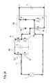
- FIG. 1 is a circuit configuration diagram of a power conversion device according to embodiment 1 of the present invention.
- the power conversion device includes a main circuit and a control unit 100 , for converting AC voltage and AC power of a single-phase AC power supply 1 to DC voltage and DC power and outputting the DC voltage and DC power to a smoothing capacitor 4 .
- the main circuit is composed of a single-phase inverter 300 , a single-phase converter 200 , and a reactor 2 connected in series to each other between the AC power supply 1 and the smoothing capacitor 4 .
- the single-phase inverter 300 includes: a DC capacitor 3 ; a first leg composed of a series body of a first switch element 5 a and a second switch element 5 b ; and a second leg composed of a series body of a third switch element 5 c and a fourth switch element 5 d , and the first leg and the second leg are connected in parallel with the DC capacitor 3 .
- the single-phase converter 200 includes: a third leg composed of a series body of a fifth switch element 6 b and a first diode 6 a ; and a fourth leg composed of a series body of a sixth switch element 6 d and a second diode 6 c , and the third leg and the fourth leg are connected in parallel to each other.
- a reactor 2 is connected between one end of the AC power supply 1 and the connection point between the first switch element 5 a and the second switch element 5 b in the single-phase inverter 300 , i.e., the center point of the first leg which is one 5 e of the inverter AC terminals of the single-phase inverter 300 .
- the center point of the second leg which is the other one 5 f of the inverter AC terminals of the single-phase inverter 300 is connected to the center point of the third leg which is one 6 e of the converter AC terminals of the single-phase converter 200 .
- the center point of the fourth leg which is the other one 6 f of the converter AC terminals of the single-phase converter 200 is connected to the other end of the AC power supply 1 .
- the upper end and the lower end of the third leg and the fourth leg are converter DC terminals 6 g , 6 h connected to the smoothing capacitor 4 .
- the control unit 100 receives voltage vac of the AC power supply 1 detected by the AC voltage detection unit 10 , current iac of the AC power supply 1 detected by the AC current detection unit 11 , voltage Vc 2 of the DC capacitor 3 detected by the DC capacitor voltage detection unit 12 , and voltage Vc 1 of the smoothing capacitor 4 detected by the DC voltage detection unit 13 , and executes control operation described in detail below, to output gate signals G 5 a to G 5 d for driving the switch elements 5 a to 5 d in the single-phase inverter 300 to perform switching and gate signals G 6 b , G 6 d for driving the switch elements 6 b , 6 d in the single-phase converter 200 to perform switching.
- a load (not shown) is connected in parallel to the smoothing capacitor 4 .
- a resistor, a voltage source such as a battery, or the like may be directly connected, or a resistor, a voltage source such as a battery, or the like may be connected via a power converter such as a DC-DC converter or a DC-AC inverter.
- the switch elements 5 a to 5 d , 6 b , 6 d are formed from MOSFETs (Metal Oxide Semiconductor Field Effect Transistors) having diodes therein. Also, the diodes 6 a , 6 c may be formed from MOSFETs.
- MOSFETs Metal Oxide Semiconductor Field Effect Transistors
- the switch elements may be formed from IGBTs (Insulated Gate Bipolar Transistors) having diodes between the sources and the drains, or semiconductor elements made from compound semiconductors such as SiC (Silicon Carbide), GaN (Galium Nitride), etc.
- IGBTs Insulated Gate Bipolar Transistors
- SiC Silicon Carbide
- GaN GaN
- the single-phase converter 200 switches the voltage level between the converter AC terminals 6 e , 6 f to a positive/negative value Vc 1 , ⁇ Vc 1 of voltage of the smoothing capacitor 4 , or zero voltage, through switching operation of the switch elements 6 b , 6 d.
- the single-phase inverter 300 switches the voltage level between the inverter AC terminals 5 e , 5 f to a positive/negative value Vc 2 , ⁇ Vc 2 of voltage of the DC capacitor 3 , or zero voltage, through switching operation of the switch elements 5 a to 5 d.
- the directions of output voltages of the single-phase converter 200 and the single-phase inverter 300 are determined depending on the relationship among voltage vac of the AC power supply 1 , voltage Vc 1 of the smoothing capacitor 4 , and voltage Vc 2 of the DC capacitor 3 .
- FIG. 2 shows a voltage relationship in the case where voltage Vc 1 of the smoothing capacitor 4 is greater than the absolute value
- operation in this case is referred to as a step-up operation mode.
- FIG. 3 shows a voltage relationship in the case where voltage Vc 1 of the smoothing capacitor 4 is smaller than the absolute value
- operation in this case is referred to as a step-down operation mode.
- Tg indicates the cycle of the AC power supply 1
- Tg/2 indicates the half cycle of the AC power supply 1
- ⁇ 1 and ⁇ 2 are phases when Vc 2 is equal to
- ⁇ 1 and ⁇ 2 are phases when Vc 1 is equal to
- areas in which phase t is in ranges of 0 ⁇ t ⁇ 1 and ⁇ 2 ⁇ t ⁇ Tg/2 are areas in which a relationship of
- An area of ⁇ 1 ⁇ t ⁇ 2 in FIG. 2 and areas of ⁇ 1 ⁇ t ⁇ 1 and ⁇ 2 ⁇ t ⁇ 2 in FIG. 3 are areas in which Vc 2 ⁇
- An area of ⁇ 1 ⁇ t ⁇ 2 in FIG. 3 is an area in which Vc 1 ⁇
- the areas 1 and 2 are referred to as area A, and the area 3 is referred to as area B.
- the current route differs between the positive half wave and the negative half wave of the AC power supply 1 . Therefore, first, driving methods (gate patterns) and current routes in the areas 1 to 3 in the positive half wave will be described, and next, driving methods and current routes in the negative half wave will be described. It is noted that the inductance of the reactor 2 is defined as L.
- the switching cycle of the single-phase inverter 300 and the switching cycle of the single-phase converter 200 are equally set to Tsw.
- FIG. 4 is an operation schematic diagram showing the operation state during one switching cycle Tsw, in the area 1 in the positive half wave of the AC power supply 1 .
- one switching cycle Tsw is divided into two pairs of periods, i.e., four periods in total, in which current
- current of the AC power supply 1 may decrease in the first half and increase in the second half.
- a current increase period and a current decrease period only have to be a pair of periods. The same applies hereafter.
- the switch elements 5 c , 6 b are ON and the AC power supply 1 is short-circuited through the single-phase converter 200 , so that current
- the current at this time flows through a route shown in FIG. 5 .
- the route is as follows: AC power supply 1 ⁇ reactor 2 ⁇ switch element 5 a ⁇ switch element 5 c ⁇ switch element 6 b ⁇ switch element 6 d ⁇ AC power supply 1 .
- a current change amount ⁇ iac11 during this period is represented by the following Expression (1) and becomes a positive value.
- ⁇ iac 11 (
- the switch elements 5 b , 5 c are ON, and a circuit is made through the smoothing capacitor 4 and thus the smoothing capacitor 4 is charged, so that current
- the current at this time flows through a route shown in FIG. 6 .
- the route is as follows: AC power supply 1 ⁇ reactor 2 ⁇ switch element 5 b ⁇ DC capacitor 3 ⁇ switch element 5 c ⁇ diode 6 a ⁇ smoothing capacitor 4 ⁇ switch element 6 d ⁇ AC power supply 1 .
- current flows through the DC capacitor 3 in a discharging direction, so that voltage Vc 2 decreases.
- a current change amount ⁇ iac12 during this period is represented by the following Expression (2) and becomes a negative value.
- ⁇ iac 12 ((
- FIG. 9 shows a schematic diagram of operation during one switching cycle Tsw, in the area 2 in the positive half wave of the AC power supply 1 .
- one switching cycle Tsw is divided into four periods and driving is performed by high-frequency PWM.
- the switch element 6 b is ON and current
- the current at this time flows through a route shown in FIG. 10 .
- the route is as follows: AC power supply 1 ⁇ reactor 2 ⁇ switch element 5 a ⁇ DC capacitor 3 ⁇ switch element 5 d ⁇ switch element 6 b ⁇ switch element 6 d ⁇ AC power supply 1 .
- current flows through the DC capacitor 3 in a charging direction, and therefore voltage Vc 2 increases.
- a current change amount ⁇ iac21 is represented by the following Expression (9) and becomes a positive value.
- ⁇ iac 21 ((
- the switch element 5 c is ON and current
- the current at this time flows through a route shown in FIG. 11 .
- the route is as follows: AC power supply 1 ⁇ reactor 2 ⁇ switch element 5 a ⁇ switch element 5 c ⁇ diode 6 a ⁇ smoothing capacitor 4 ⁇ switch element 6 d ⁇ AC power supply 1 .
- current does not flow through the DC capacitor 3 , and therefore voltage Vc 2 is constant.
- the current change amount ⁇ iac22 during this period is represented by the following Expression (10) and becomes a negative value.
- ⁇ iac 22 ((
- the switch element 5 c is ON and current
- the current at this time flows through a route shown in FIG. 13 .
- the route is as follows: AC power supply 1 ⁇ reactor 2 ⁇ switch element 5 a ⁇ switch element 5 c ⁇ diode 6 a ⁇ smoothing capacitor 4 ⁇ switch element 6 d ⁇ AC power supply 1 .
- current does not flow through the DC capacitor 3 , and therefore voltage Vc 2 is constant.
- a current change amount ⁇ iac24 during this period is represented by the following Expression (12) and becomes a negative value.
- ⁇ iac 24 ((
- FIG. 14 shows a schematic diagram of operation during one switching cycle Tsw, in the area 3 in a positive half wave of the AC power supply 1 .
- one switching cycle Tsw is divided into two periods and driving is performed by high-frequency PWM.
- the switch elements 5 b , 5 c are ON and current
- the current at this time flows through a route shown in FIG. 15 .
- the route is as follows: AC power supply 1 ⁇ reactor 2 ⁇ switch element 5 b ⁇ DC capacitor 3 ⁇ switch element 5 c ⁇ diode 6 a ⁇ smoothing capacitor 4 ⁇ switch element 6 d ⁇ AC power supply 1 .
- current flows through the DC capacitor 3 in a discharging direction, and therefore voltage Vc 2 decreases.
- the current change amount ⁇ iac31 during this period is represented by the following Expression (17) and becomes a positive value.
- ⁇ iac 31 ((
- FIG. 17 shows a schematic diagram of operation during a one switching cycle Tsw, in the area 1 in the negative half wave of the AC power supply 1 .
- One switching cycle Tsw is divided into four periods and driving is performed by high-frequency PWM.
- the switch elements 5 a , 6 d are ON and current
- the current at this time flows through a route shown in FIG. 18 .
- the route is as follows: AC power supply 1 ⁇ switch element 6 d ⁇ switch element 6 b ⁇ switch element 5 c ⁇ switch element 5 a ⁇ reactor ⁇ AC power supply 1 .
- a current change amount ⁇ iac11 during this period is represented by the following Expression (21) and becomes a positive value.
- ⁇ iac 11 (
- the switch elements 5 a , 6 d are ON and current
- the current at this time flows through a route shown in FIG. 20 .
- the route is as follows: AC power supply 1 ⁇ switch element 6 d ⁇ switch element 6 b ⁇ switch element 5 c ⁇ switch element 5 a ⁇ reactor 2 ⁇ AC power supply 1 .
- a current change amount ⁇ iac13 during this period is represented by the following Expression (23) and becomes a positive value.
- ⁇ iac 13 (
- the switch element 6 d is ON and current
- the current at this time flows through a route shown in FIG. 21 .
- the route is as follows: AC power supply 1 ⁇ switch element 6 d ⁇ switch element 6 b ⁇ switch element 5 c ⁇ DC capacitor 3 ⁇ switch element 5 b ⁇ reactor 2 ⁇ AC power supply 1 .
- a current change amount ⁇ iac14 during this period is represented by the following Expression (24) and becomes a negative value.
- ⁇ iac 14 ((
- FIG. 22 shows a schematic diagram of operation during one switching cycle Tsw, in the area 2 in the negative half wave of the AC power supply 1 .
- One switching cycle Tsw is divided into four periods and driving is performed by high-frequency PWM.
- the switch element 6 d is ON and current
- the current at this time flows through a route shown in FIG. 23 .
- the route is as follows: AC power supply 1 ⁇ switch element 6 d ⁇ switch element 6 b ⁇ switch element 5 c ⁇ DC capacitor 3 ⁇ switch element 5 b ⁇ reactor 2 ⁇ AC power supply 1 .
- a current change amount ⁇ iac21 during this period is represented by the following Expression (29) and becomes a positive value.
- ⁇ iac 21 ((
- the switch element 5 a is ON and current
- the current at this time flows through a route shown in FIG. 24 .
- the route is as follows: AC power supply 1 ⁇ diode 6 c ⁇ smoothing capacitor 4 ⁇ switch element 6 b ⁇ switch element 5 c ⁇ switch element 5 a ⁇ reactor 2 ⁇ AC power supply 1 .
- current does not flow through the DC capacitor 3 , and therefore voltage Vc 2 is constant.
- a current change amount ⁇ iac22 during this period is represented by the following Expression (30) and becomes a negative value.
- ⁇ iac 22 ((
- the switch elements 5 a , 5 d are ON and current
- the current at this time flows through a route shown in FIG. 25 .
- the route is as follows: AC power supply 1 ⁇ diode 6 c ⁇ smoothing capacitor 4 ⁇ switch element 6 b ⁇ switch element 5 d ⁇ DC capacitor 3 ⁇ switch element 5 a ⁇ reactor 2 ⁇ AC power supply 1 .
- a current change amount ⁇ iac23 during this period is represented by the following Expression (31) and becomes a positive value.
- the switch element 5 a is ON and current
- the current at this time flows through a route shown in FIG. 26 .
- the route is as follows: AC power supply 1 ⁇ diode 6 c ⁇ smoothing capacitor 4 ⁇ switch element 6 b ⁇ switch element 5 c ⁇ switch element 5 a ⁇ reactor 2 ⁇ AC power supply 1 .
- current does not flow through the DC capacitor 3 , and therefore voltage Vc 2 is constant.
- a current change amount ⁇ iac22 during this period is represented by the following Expression (32) and becomes a negative value.
- ⁇ iac 24 ((
- FIG. 27 shows a schematic diagram of operation during one switching cycle Tsw, in the area 3 in the negative half wave of the AC power supply 1 .
- One switching cycle Tsw is divided into two periods and driving is performed by high-frequency PWM.
- the switch elements 5 a , 5 d are ON and current
- the current at this time flows through a route shown in FIG. 28 .
- the route is as follows: AC power supply 1 ⁇ diode 6 c ⁇ smoothing capacitor 4 ⁇ switch element 6 b ⁇ switch element 5 d ⁇ DC capacitor 3 ⁇ switch element 5 a ⁇ reactor 2 ⁇ AC power supply 1 .
- a current change amount ⁇ iac31 during this period is represented by the following Expression (37) and becomes a positive value.
- ⁇ iac 31 ((
- the frequency of the AC power supply 1 is 50 to 60 Hz, whereas the switching frequency of the single-phase inverter 300 is generally 10 kHz or higher. Therefore, from the above, irrespective of a very long cycle of the AC power supply 1 , charging operation and discharging operation of the DC capacitor 3 are completed within one short switching cycle of the single-phase inverter 300 , and thus the charging/discharging amount itself is reduced and ripple voltage is suppressed, whereby the capacitance required for the DC capacitor 3 can be greatly reduced.
- the application voltage frequency of the reactor 2 is twice the switching frequency (1/Tsw) of the single-phase inverter 300 , whereby size reduction of the reactor 2 can be achieved.
- control unit 100 serving to generate gate signals for driving the switch elements to perform switching, in order to actually ensure the relationships of the theoretical duties, will be described with reference to FIG. 30 and the subsequent figures.
- the control unit 100 includes a theoretical duty calculator 110 , a feedback duty calculator 120 , an adder/subtractor 130 , a gate signal calculator 140 , an operation area determiner 150 , and a gate signal selector 160 .
- the theoretical duty calculator 110 includes an area-1 theoretical duty calculator 111 , an area-2 theoretical duty calculator 112 , and an area-3 theoretical duty calculator 113 , and calculates theoretical duties using the theoretical expressions in the areas 1 to 3.
- the area-1 theoretical duty calculator 111 calculates the theoretical duties D11 to D14 using Expressions (5) to (8) or Expressions (25) to (28).
- the area-2 theoretical duty calculator 112 calculates the theoretical duties D21 to D24 using Expressions (13) to (16) or Expressions (33) to (36).
- the area-3 theoretical duty calculator 113 calculates the theoretical duties D31 and D32 using Expressions (19) and (20) or Expressions (39) and (40).
- Each theoretical duty is calculated on the basis of: voltage vac of the AC power supply 1 which is a detection value of the AC voltage detection unit 10 , or an ideal voltage value vac* of the AC power supply 1 ; voltage Vc 2 of the DC capacitor 3 which is a detection value of the DC capacitor voltage detection unit 12 , or a voltage command value vc 2 * for the DC capacitor 3 ; and voltage Vc 1 of the smoothing capacitor 4 which is a detection value of the DC voltage detection unit 13 , or a voltage command value Vc 1 * for the smoothing capacitor 4 .
- FIG. 30 shows a case of performing the calculation on the basis of the detection values of the respective voltage detection units.
- the feedback duty calculator 120 is configured as shown in FIG. 31 .
- a deviation between the DC voltage detection value Vc 1 of the smoothing capacitor 4 and the command value Vc 1 * therefor is calculated by a subtractor, and then, PI control is performed by a PI controller, and the resultant value is subjected to a limiter, whereby a current amplitude command value ⁇ 2Iac* for the AC power supply 1 is calculated.
- a phase ⁇ synchronized with the phase of vac is calculated by PLL (Phase Locked Loop). Then, a sine wave with the phase ⁇ is multiplied with the current amplitude command value ⁇ 2Iac* for the AC power supply 1 , whereby an AC current command value iac* for the AC power supply 1 is calculated.
- the adder/subtractor 130 adds or subtracts the feedback duty DFB to or from the calculation results of the theoretical duty calculator 110 . Since control is performed in such a direction as to increase current iac of the AC power supply 1 when the DFB increases, the DFB is added to D11, D13, D21, D23, D31 by the adders 131 , 133 , 135 , and the DFB is subtracted from D12, D14, D22, D24, D32 by the subtractors 132 , 134 , 136 . These calculation results are inputted to the gate signal calculator 140 .
- FIG. 32 is a configuration diagram of the gate signal calculator 140 .
- the gate signal calculator 140 includes an area-1 gate signal calculator 141 , an area-2 gate signal calculator 142 , and an area-3 gate signal calculator 143 , and calculates gate signals for each switching cycle, from the inputted duties.
- the area-1 gate signal calculator 141 includes four comparators and a carrier signal cararea 1 , and compares D11+DFB, D12 ⁇ DFB, D13+DFB, and D14 ⁇ DFB which are input signals, with the carrier signal cararea 1 , by the respective comparators, thereby generating a signal G 11 for the first period, a signal G 12 for the second period, a signal G 13 for the third period, and a signal G 14 for the fourth period.
- the area-2 gate signal calculator 142 includes two comparators and a carrier signal cararea 2 , and compares D21+DFB, D22 ⁇ DFB, D23+DFB, and D24 ⁇ DFB which are input signals, with the carrier signal cararea 2 , by the respective comparators, thereby generating a signal G 21 for the first period, a signal G 22 for the second period, a signal G 23 for the third period, and a signal G 24 for the fourth period.
- the area-3 gate signal calculator 143 includes two comparators and a carrier signal cararea 3 , and compares D31+DFB and D32 ⁇ DFB which are input signals, with the carrier signal cararea 3 , by the respective comparators, thereby generating a signal G 31 for the first period and a signal G 32 for the second period.
- the above signals are inputted to the gate signal selector 160 , and thus are distributed as gate signals for the respective switch elements.
- An absolute value calculator 170 calculates the absolute value
- the operation area determiner 150 performs magnitude comparison among the absolute value
- the DC capacitor voltage command value Vc 2 * may be used.
- the gate signal selector 160 allocates outputs of the gate signal calculator 140 to the switch elements, using the area signal sigarea outputted from the operation area determiner 150 .
- the control unit 100 shown in FIG. 30 performs control such that, in the area 1 and the area 2, one switching cycle is divided into four periods, and in the area 3, one switching cycle is divided into two periods.
- FIG. 33 shows a gate pattern diagram in the area 1 in the positive half wave.
- FIG. 34 shows a gate pattern diagram in the area 3 in the positive half wave.
- 1 cycle and 1 ⁇ 2 cycle of the switching cycle are made constant, and an ON period ratio during those periods is controlled. That is, in FIG. 33 , times 0, t12, Tsw are fixed, and t11 and t13 are controlled by the control unit 100 .
- t11 and t13 correspond to timings that determine the boundaries between the current increase period and the current decrease period regarding the current of the AC power supply 1 , and are referred to as control axes in claims of the present disclosure. The same applies to t31 and the like described below.
- one cycle of the switching cycle is made constant and an ON period ratio during that period is controlled.
- the switching cycle as a reference is constant, and PWM (Pulse Width Modulation) control can be used.
- One cycle of the switching cycle is made constant and an ON period ratio during that period is controlled. That is, in FIG. 34 , times 0 and Tsw are fixed and t31 is controlled.
- the control unit 100 of the power conversion device in embodiment 1 of the present invention performs control such that one switching cycle Tsw of the single-phase inverter 300 is the same as one switching cycle Tsw of the single-phase converter 200 and is divided into an even number of periods including one or two pairs of periods in which current of the AC power supply 1 increases in the first half of each pair of periods and decreases in the second half of each pair of periods, and the control unit 100 includes: the theoretical duty calculator 110 which calculates the theoretical duty 1 corresponding to the first-half time width relative to the time width of one pair of periods, and the theoretical duty 2 corresponding to the second-half time width relative to the time width of one pair of periods, so that the increase amount of current of the AC power supply 1 in the first half and the decrease amount thereof in the second half become equal to each other in the one pair of periods; and the gate signal calculator 140 which calculates gate signals for driving the switch elements of the single-phase inverter 300 and the switch elements of the single-phase converter 200 to perform switching, on the basis of the theoretical duty 1
- charging operation and discharging operation of the DC capacitor 3 are performed within one switching cycle of the single-phase inverter 300 , and the charging amount and the discharging amount become equal to each other. Therefore, irrespective of the very long cycle of the AC power supply 1 , charging operation and discharging operation of the DC capacitor 3 are completed within one short switching cycle of the single-phase inverter 300 , whereby the charging/discharging amount itself is reduced, the capacitance required for the DC capacitor 3 in order to suppress ripple voltage can be greatly reduced, and size reduction of the device can be achieved.
- control unit 100 includes: a voltage controller which generates an AC current command value on the basis of a deviation between the DC voltage command value and the DC voltage detection value; and the feedback duty calculator 120 which calculates the feedback duty on the basis of a deviation between the AC current command value and an AC current detection value, and the gate signal calculator 140 calculates the gate signals on the basis of duties calculated by adding the feedback duty to the theoretical duty 1 and by subtracting the feedback duty from the theoretical duty 2. Therefore, it becomes possible to perform constant-voltage control so as to keep voltage of the smoothing capacitor 4 at a desired DC voltage command value.
- control unit 100 sets the number of divided periods in one switching cycle of the single-phase inverter 300 in accordance with the areas 1, 2, 3 determined depending on the magnitude relationship among voltage vac of the AC power supply 1 , voltage Vc 1 of the smoothing capacitor 4 , and voltage Vc 2 of the DC capacitor 3 . Therefore, it becomes possible to perform switching control for each switch element by an appropriate gate pattern according to the voltage relationship.
- control unit 100 controls the switch elements such that switching timings are different between the single-phase inverter 300 and the single-phase converter 200 . Therefore, it becomes possible to make the application voltage frequency of the reactor 2 higher than the switching frequencies of the single-phase inverter 300 and the single-phase converter 200 .
- the inductance value is to be reduced through reduction in core size and decrease in the number of winding turns. Therefore, size reduction of the reactor 2 is achieved as a result.
- the upper arms of the single-phase converter 200 are composed of diodes 6 a , 6 c .
- the upper arms may be composed of switch elements (substitute switch elements). In this case, by turning on the switch elements during the conduction periods of the diodes 6 a , 6 c shown in embodiment 1, it is possible to perform so-called synchronous rectification operation.
- the switching cycles Tsw in the area 1, the area 2, and the area 3 may have the same constant value or may have respective independent values.
- the switching cycles in the area 1 and the area 2 may be set at the same constant value, and the switching cycle in the area 3 may be set to be half the switching cycle in the area 1 and the area 2.
- the application voltage frequency of the reactor 2 becomes constant in all the areas. If the application voltage frequency is constant, it becomes easy to take measures for noise and establish stable control.
- driving may be performed using PFM (Pulse Frequency Modulation) control in which the switching frequency is varied while the ON period of any of the switch elements is fixed.
- the reactor 2 is provided on the positive-side line of the AC power supply 1 . However, the reactor 2 may be connected on only the negative-side line, or may be connected on both the positive-side line and the negative-side line.
- the reactor may be connected between the single-phase inverter 300 and the single-phase converter 200 .
- the single-phase inverter 300 is provided on the positive-side line of the AC power supply 1 , the single-phase inverter 300 may be provided on the negative-side line.
- a configuration having a diode bridge 500 which is a rectification circuit may be employed.
- both ends of the AC power supply 1 are connected to AC terminals of the diode bridge 500
- the reactor 2 , the single-phase inverter 300 , and the AC terminal of the single-phase converter 200 are connected in series to the positive-side DC output terminal.
- the negative-side DC output terminal of the diode bridge 500 is connected to the source terminal of the switch element 6 b of the single-phase converter 200 and one terminal of the smoothing capacitor 4 .
- the other terminal of the smoothing capacitor 4 is connected to the cathode terminal of the diode 6 a of the single-phase converter 200 .
- driving can be performed using only the control for the positive half wave in the configuration shown in FIG. 1 , and obtained effects are the same as in the case of FIG. 1 .
- the reactor 2 may be connected on at least one of the positive-side line and the negative-side line between the AC power supply 1 and the diode bridge 500 , or may be connected between the single-phase inverter 300 and the single-phase converter 200 .
- the feedback duty calculator 120 shown in FIG. 31 may perform only current control using a predetermined current amplitude command value ⁇ 2Iac* for the AC power supply 1 without performing Vc 1 -constant control.
- the AC power supply may be a three-phase power supply.
- the single-phase inverters shown in FIG. 1 are provided for three phases, and one of inverter AC terminals of the single-phase inverter for each phase is connected to the terminal for the corresponding phase of the three-phase power supply via a reactor for the corresponding phase.
- the converter is configured as a three-phase converter in which: legs for three phases are provided each of which is composed of a series body of the switch element and the diode; the converter AC terminal for each phase which corresponds to the middle point of the leg for each phase is connected to the other one of the inverter AC terminals of the single-phase inverter for the corresponding phase; and the converter DC terminals corresponding to the upper end and the lower end of the leg for each phase are connected to the smoothing capacitor.
- FIG. 36 is a circuit configuration diagram of a power conversion device according to embodiment 2 of the present invention.
- the power conversion device includes a main circuit and the control unit 100 , for converting AC voltage and AC power of the AC power supply 1 to DC voltage and DC power and outputting the DC voltage and DC power to the smoothing capacitor 4 .
- the main circuit includes a single-phase inverter 400 connected to the lower end of the AC power supply 1 , in addition to the single-phase inverter 300 having the inverter AC terminal 5 e connected to the upper end of the AC power supply 1 via a reactor 2 a.
- the single-phase inverter 400 has the same configuration as the single-phase inverter 300 , that is, includes the DC capacitor 9 and two legs respectively composed of series bodies of pairs of switch elements 8 a , 8 b and 8 c , 8 d , and an inverter AC terminal 8 e corresponding to the middle point of one of the legs is connected to the lower end of the AC power supply 1 via a reactor 2 b.
- the inverter AC terminal 5 f of the single-phase inverter 300 is connected to the converter AC terminal 6 e of the single-phase converter 200 , and an inverter AC terminal 8 f corresponding to the middle point of the other leg of the single-phase inverter 400 is connected to the converter AC terminal 6 f of the single-phase converter 200 .
- the control unit 100 receives voltage Vc 3 of the DC capacitor 9 detected by a DC capacitor voltage detection unit 14 , as well as voltage vac of the AC power supply 1 , current iac of the AC power supply 1 , voltage Vc 2 of the DC capacitor 3 , and voltage Vc 1 of the smoothing capacitor 4 , and outputs gate signals G 8 a to G 8 d for driving the switch elements 8 a to 8 d of the single-phase inverter 400 to perform switching, as well as the gate signals G 5 a to G 5 d for driving the switch elements 5 a to 5 d of the single-phase inverter 300 to perform switching, and the gate signals G 6 b , G 6 d for driving the switch elements 6 b , 6 d of the single-phase converter 200 to perform switching.
- the single-phase inverter 400 switches the voltage level between the inverter AC terminals 8 e , 8 f to a positive/negative value Vc 3 , ⁇ Vc 3 of voltage of the DC capacitor 9 , or zero voltage, through switching operation of the switch elements 8 a to 8 d.
- the directions of output voltages of the single-phase converter 200 , the single-phase inverter 300 , and the single-phase inverter 400 are determined-depending on the relationship among voltage vac of the AC power supply 1 , voltage Vc 1 of the smoothing capacitor 4 , voltage Vc 2 of the DC capacitor 3 , and voltage Vc 3 of the DC capacitor 9 .
- voltage Vc 2 of the DC capacitor 3 and voltage Vc 3 of the DC capacitor 9 are smaller than voltage Vc 1 of the smoothing capacitor 4 .
- FIG. 37 and FIG. 38 are diagrams obtained by redrawing FIG. 2 and FIG. 3 in the above embodiment 1 so as to be adapted to the present embodiment 2.
- areas in which phase t is in ranges of 0 ⁇ t ⁇ 1 and ⁇ 2 ⁇ t ⁇ Tg/2 are areas in which a relationship of
- An area of ⁇ 1 ⁇ t ⁇ 2 in FIG. 37 and areas of ⁇ 1 ⁇ t ⁇ 1 and ⁇ 2 ⁇ t ⁇ 2 in FIG. 38 are areas in which Vsub ⁇
- An area of ⁇ 1 ⁇ t ⁇ 2 in FIG. 38 is an area in which Vc 1 ⁇
- the current route differs between the positive half wave and the negative half wave of the AC power supply 1 . Therefore, first, driving methods (gate patterns) and current routes in the areas 1 to 3 in the positive half wave will be described, and next, driving methods and current routes in the negative half wave will be described. It is noted that the total inductance of the reactors 2 a and 2 b is defined as L.
- a switching cycle 2Tsw of the single-phase inverters 300 , 400 is twice the switching cycle Tsw of the single-phase converter 200 .
- FIG. 39 is an operation schematic diagram showing the operation state during one switching cycle 2Tsw (two switching cycles of the converter) of the inverters, in the area 1 in the positive half wave of the AC power supply 1 .
- the switching cycle Tsw in the first half the single-phase inverter 300 and the single-phase converter 200 operate, and in the switching cycle Tsw in the second half, the single-phase inverter 400 and the single-phase converter 200 operate.
- the switching cycle Tsw is divided into four periods and driving is performed by high-frequency PWM.
- the switch elements 5 c , 6 b , 8 a are ON and current
- the current at this time flows through a route shown in FIG. 40 .
- the route is as follows: AC power supply 1 ⁇ reactor 2 a ⁇ switch element 5 a ⁇ switch element 5 c ⁇ switch element 6 b ⁇ switch element 6 d ⁇ switch element 8 c ⁇ switch element 8 a ⁇ reactor 2 b ⁇ AC power supply 1 .
- a current change amount ⁇ iac11 during this period is represented by the following Expression (41) and becomes a positive value.
- ⁇ iac 11 (
- the switch elements 5 b , 5 c , 8 a are ON and current
- the current at this time flows through a route shown in FIG. 41 .
- the route is as follows: AC power supply 1 ⁇ reactor 2 a ⁇ switch element 5 b ⁇ DC capacitor 3 ⁇ switch element 5 c ⁇ diode 6 a ⁇ smoothing capacitor 4 ⁇ switch element 6 d ⁇ switch element 8 c ⁇ switch element 8 a ⁇ reactor 2 b ⁇ AC power supply 1 .
- a current change amount ⁇ iac12 during this period is represented by the following Expression (42) and becomes a negative value.
- ⁇ iac 12 ((
- the switch elements 5 c , 6 b , 8 a are ON and current
- the current at this time flows through a route shown in FIG. 42 .
- the route is as follows: AC power supply 1 ⁇ reactor 2 a ⁇ switch element 5 a ⁇ switch element 5 c ⁇ switch element 6 b ⁇ switch element 6 d ⁇ switch element 8 c ⁇ switch element 8 a ⁇ reactor 2 b ⁇ AC power supply 1 .
- a current change amount ⁇ iac13 during this period is represented by the following Expression (43) and becomes a positive value.
- ⁇ iac 13 (
- the switch elements 6 b , 8 a are ON and current
- the current at this time flows through a route shown in FIG. 43 .
- the route is as follows: AC power supply 1 ⁇ reactor 2 a ⁇ switch element 5 a ⁇ DC capacitor 3 switch element 5 d ⁇ switch element 6 b ⁇ switch element 6 d ⁇ switch element 8 c ⁇ switch element 8 a ⁇ reactor 2 b ⁇ AC power supply 1 .
- the switch elements 5 c , 8 a , 8 d are ON and current
- the current at this time flows through a route shown in FIG. 45 .
- the route is as follows: AC power supply 1 ⁇ reactor 2 a ⁇ switch element 5 a ⁇ switch element 5 c ⁇ diode 6 a ⁇ smoothing capacitor 4 ⁇ switch element 6 d ⁇ switch element 8 d ⁇ DC capacitor 9 ⁇ switch element 8 a ⁇ reactor 2 b ⁇ AC power supply 1 .
- a current change amount ⁇ iac16 during this period is represented by the following Expression (46) and becomes a negative value.
- ⁇ iac 16 ((
- the switch elements 5 c , 6 b , 8 a are ON and current
- the current at this time flows through a route shown in FIG. 46 .
- the route is as follows: AC power supply 1 ⁇ reactor 2 a ⁇ switch element 5 a ⁇ switch element 5 c ⁇ switch element 6 b ⁇ , switch element 6 d ⁇ switch element 8 c ⁇ switch element 8 a ⁇ reactor 2 b ⁇ AC power supply 1 .
- current does not flow through the DC capacitor 3 and the DC capacitor 9 , and therefore voltages Vc 2 and Vc 3 are constant.
- a current change amount ⁇ iac17 during this period is represented by the following Expression (47) and becomes a positive value.
- ⁇ iac 17 (
- the switch elements 5 c , 6 b are ON and current
- the current at this time flows through a route shown in FIG. 47 .
- the route is as follows: AC power supply 1 ⁇ reactor 2 a ⁇ switch element 5 a ⁇ switch element 5 c ⁇ switch element 6 b ⁇ switch element 6 d ⁇ switch element 8 c ⁇ DC capacitor 9 ⁇ switch element 8 b ⁇ reactor 2 b ⁇ AC power supply 1 .
- FIG. 48 shows a schematic diagram of operation during the switching cycle 2Tsw, in the area 2 in the positive half wave of the AC power supply 1 .
- the switching cycle Tsw in the first half the single-phase inverter 300 and the single-phase converter 200 operate, and in the switching cycle Tsw in the second half, the single-phase inverter 400 and the single-phase converter 200 operate.
- the switching cycle Tsw is divided into four periods and driving is performed by high-frequency PWM.
- the switch elements 6 b , 8 a are ON and current
- the current at this time flows through a route shown in FIG. 49 .
- the route is as follows: AC power supply 1 ⁇ reactor 2 a ⁇ switch element 5 a ⁇ DC capacitor 3 ⁇ switch element 5 d ⁇ switch element 6 b ⁇ switch element 6 d ⁇ switch element 8 c ⁇ switch element 8 a ⁇ reactor 2 b ⁇ AC power supply 1 .
- a current change amount ⁇ iac21 during this period is represented by the following Expression (57) and becomes a positive value.
- ⁇ iac 21 ((
- the switch elements 5 c , 8 a are ON and current
- the current at this time flows through a route shown in FIG. 50 .
- the route is as follows: AC power supply 1 ⁇ reactor 2 a ⁇ switch element 5 a ⁇ switch element 5 c ⁇ diode 6 a ⁇ smoothing capacitor 4 ⁇ switch element 6 d ⁇ switch element 8 c ⁇ switch element 8 a ⁇ reactor 2 b ⁇ AC power supply 1 .
- current does not flow through the DC capacitor 3 and the DC capacitor 9 , and therefore voltages Vc 2 and Vc 3 are constant.
- a current change amount ⁇ iac22 during this period is represented by the following Expression (58) and becomes a negative value.
- the switch elements 5 b , 5 c , 8 a are ON and current
- the current at this time flows through a route shown in FIG. 51 .
- the route is as follows: AC power supply 1 ⁇ reactor 2 a ⁇ switch element 5 b ⁇ DC capacitor 3 ⁇ switch element 5 c ⁇ diode 6 a ⁇ smoothing capacitor 4 ⁇ switch element 6 d ⁇ switch element 8 c ⁇ switch element 8 a ⁇ reactor 2 b ⁇ AC power supply 1 .
- a current change amount ⁇ iac23 during this period is represented by the following Expression (59) and becomes a positive value.
- ⁇ iac 23 ((
- the switch elements 5 c , 6 b are ON and current
- the current at this time flows through a route shown in FIG. 53 .
- the route is as follows: AC power supply 1 ⁇ reactor 2 a ⁇ switch element 5 a ⁇ switch element 5 c ⁇ switch element 6 b ⁇ switch element 6 d ⁇ switch element 8 c ⁇ DC capacitor 9 ⁇ switch element 8 b ⁇ reactor 2 b ⁇ AC power supply 1 .
- a current change amount ⁇ iac25 during this period is represented by the following Expression (61) and becomes a positive value.
- ⁇ iac 25 ((
- the switch elements 5 c , 8 a are ON and current
- the switch elements 5 c , 8 a , 8 d are ON and current
- the current at this time flows through a route shown in FIG. 55 .
- the route is as follows: AC power supply 1 ⁇ reactor 2 a ⁇ switch element 5 a ⁇ switch element 5 c ⁇ diode 6 a ⁇ smoothing capacitor 4 ⁇ switch element 6 d ⁇ switch element 8 d ⁇ DC capacitor 9 ⁇ switch element 8 a ⁇ reactor 2 b ⁇ AC power supply 1 .
- a current change amount ⁇ iac27 during this period is represented by the following Expression (63) and becomes a positive value.
- ⁇ iac 27 ((
- the switch elements 5 c , 8 a are ON and current
- the current at this time flows through a route shown in FIG. 56 .
- the current is as follows: AC power supply 1 ⁇ reactor 2 a ⁇ switch element 5 a ⁇ switch element 5 c ⁇ diode 6 a ⁇ smoothing capacitor 4 ⁇ switch element 6 d ⁇ switch element 8 c ⁇ switch element 8 a ⁇ reactor 2 b ⁇ AC power supply 1 .
- a current change amount ⁇ iac28 during this period is represented by the following Expression (64) and becomes a negative value.
- ⁇ iac 28 ((
- FIG. 57 shows a schematic diagram of operation during the switching cycle 2Tsw, in the area 3 in the positive half wave of the AC power supply 1 .
- the single-phase inverter 300 operates, and in the switching cycle Tsw in the second half, the single-phase inverter 400 operates.
- the switching cycle Tsw is divided into two periods and driving is performed by high-frequency PWM.
- the switch elements 5 b , 5 c , 8 a are ON and current
- the current at this time flows through a route shown in FIG. 58 .
- the route is as follows: AC power supply 1 ⁇ reactor 2 a ⁇ switch element 5 b ⁇ DC capacitor 3 ⁇ switch element 5 c ⁇ diode 6 a ⁇ smoothing capacitor 4 ⁇ switch element 6 d ⁇ switch element 8 c ⁇ switch element 8 a ⁇ reactor 2 b ⁇ AC power supply 1 .
- a current change amount ⁇ iac31 during this period is represented by the following Expression (73) and becomes a positive value.
- ⁇ iac 31 ((
- the switch element 8 a is ON and current
- the current at this time flows through a route shown in FIG. 59 .
- the route is as follows: AC power supply 1 ⁇ reactor 2 a ⁇ switch element 5 a ⁇ DC capacitor 3 ⁇ switch element 5 d ⁇ diode 6 a ⁇ smoothing capacitor 4 ⁇ switch element 6 d ⁇ switch element 8 c ⁇ switch element 8 a ⁇ reactor 2 b ⁇ AC power supply 1 .
- a current change amount ⁇ iac32 during this period is represented by the following Expression (74) and becomes a negative value.
- ⁇ iac 32 ((
- the switch elements 5 c , 8 a , 8 d are ON and current
- the current at this time flows through a route shown in FIG. 60 .
- the route is as follows: AC power supply 1 ⁇ reactor 2 a ⁇ switch element 5 a ⁇ switch element 5 c ⁇ diode 6 a ⁇ smoothing capacitor 4 ⁇ switch element 6 d ⁇ switch element 8 d ⁇ DC capacitor 9 ⁇ switch element 8 a ⁇ reactor 2 b ⁇ AC power supply 1 .
- a current change amount ⁇ iac33 during this period is represented by the following Expression (75) and becomes a positive value.
- ⁇ iac 33 ((
- the switch element 5 c is ON and current
- the current at this time flows through a route shown in FIG. 61 .
- the route is as follows: AC power supply 1 reactor 2 a ⁇ switch element 5 a ⁇ switch element 5 c ⁇ diode 6 a ⁇ smoothing capacitor 4 ⁇ switch element 6 d ⁇ switch element 8 c ⁇ DC capacitor 9 ⁇ switch element 8 b ⁇ reactor 2 b ⁇ AC power supply 1 .
- a current change amount ⁇ iac34 during this period is represented by the following Expression (76) and becomes a negative value.
- ⁇ iac 34 ((
- FIG. 62 shows a schematic diagram of operation during the switching cycle 2Tsw, in the area 1 in the negative half wave of the AC power supply 1 .
- the switching cycle Tsw in the first half the single-phase inverter 300 and the single-phase converter 200 operate, and in the switching cycle Tsw in the second half, the single-phase inverter 400 and the single-phase converter 200 operate.
- the switching cycle Tsw is divided into four periods and driving is performed by high-frequency PWM.
- the switch elements 5 a , 6 d , 8 c are ON and current
- the current at this time flows through a route shown in FIG. 63 .
- the route is as follows: AC power supply 1 ⁇ reactor 2 b ⁇ switch element 8 a ⁇ switch element 8 c ⁇ switch element 6 d ⁇ switch element 6 b ⁇ switch element 5 c ⁇ switch element 5 a ⁇ reactor 2 a ⁇ AC power supply 1 .
- a current change amount ⁇ iac11 during this period is represented by the following Expression (81) and becomes a positive value.
- the switch elements 5 a , 5 d , 8 c are ON and current
- the current at this time flows through a route shown in FIG. 64 .
- the route is as follows: AC power supply 1 ⁇ reactor 2 b ⁇ switch element 8 a ⁇ switch element 8 c ⁇ diode 6 c ⁇ smoothing capacitor 4 ⁇ switch element 6 b ⁇ switch element 5 d ⁇ DC capacitor 3 ⁇ switch element 5 a ⁇ reactor 2 a ⁇ AC power supply 1 .
- a current change amount ⁇ iac12 during this period is represented by the following Expression (82) and becomes a negative value.
- ⁇ iac 12 ((
- the switch elements 5 a , 6 d , 8 c are ON and current
- the current at this time flows through a route shown in FIG. 65 .
- the route is as follows: AC power supply 1 ⁇ reactor 2 b ⁇ switch element 8 a ⁇ switch element 8 c ⁇ switch element 6 d ⁇ switch element 6 b ⁇ switch element 5 c ⁇ switch element 5 a ⁇ reactor 2 a ⁇ AC power supply 1 .
- a current change amount ⁇ iac13 during this period is represented by the following Expression (83) and becomes a positive value.
- ⁇ iac 13 (
- the switch elements 6 d , 8 c are ON and current
- the current at this time flows through a route shown in FIG. 66 .
- the route is as follows: AC power supply 1 ⁇ reactor 2 b ⁇ switch element 8 a ⁇ switch element 8 c ⁇ switch element 6 d ⁇ switch element 6 b ⁇ switch element 5 c ⁇ DC capacitor 3 ⁇ switch element 5 b ⁇ reactor 2 a ⁇ AC power supply 1 .
- a current change amount ⁇ iac14 during this period is represented by the following Expression (84) and becomes a negative value.
- ⁇ iac 14 ((
- the switch elements 5 a , 6 d , 8 c are ON and current
- the current at this time flows through a route shown in FIG. 67 .
- the route is as follows: AC power supply 1 ⁇ reactor 2 b ⁇ switch element 8 a ⁇ switch element 8 c ⁇ switch element 6 d ⁇ switch element 6 b ⁇ switch element 5 c ⁇ switch element 5 a ⁇ reactor 2 a ⁇ AC power supply 1 .
- a current change amount ⁇ iac15 during this period is represented by the following Expression (85) and becomes a positive value.
- the switch elements 5 a , 8 b , 8 c are ON and current
- the current at this time flows through a route shown in FIG. 68 .
- the route is as follows: AC power supply 1 ⁇ reactor 2 b ⁇ switch element 8 b ⁇ DC capacitor 9 ⁇ switch element 8 c ⁇ diode 6 c ⁇ smoothing capacitor 4 ⁇ switch element 6 b ⁇ switch element 5 c ⁇ switch element 5 a ⁇ reactor 2 a ⁇ AC power supply 1 .
- a current change amount ⁇ iac16 during this period is represented by the following Expression (86) and becomes a negative value.
- the switch elements 5 a , 6 d , 8 c are ON and current
- the current at this time flows through a route shown in FIG. 69 .
- the route is as follows: AC power supply 1 ⁇ reactor 2 b ⁇ switch element 8 a ⁇ switch element 8 c ⁇ switch element 6 d ⁇ switch element 6 b ⁇ switch element 5 c ⁇ switch element 5 a ⁇ reactor 2 a ⁇ AC power supply 1 .
- a current change amount ⁇ iac17 during this period is represented by the following Expression (87) and becomes a positive value.
- ⁇ iac 17 (
- the switch elements 5 a , 6 d are ON and current
- the current at this time flows through a route shown in FIG. 70 .
- the route is as follows: AC power supply 1 ⁇ reactor 2 b ⁇ switch element 8 a ⁇ DC capacitor 9 ⁇ switch element 8 d ⁇ switch element 6 d ⁇ switch element 6 b ⁇ switch element 5 c ⁇ switch element 5 a ⁇ reactor 2 a ⁇ AC power supply 1 .
- FIG. 71 shows a schematic diagram of operation during the switching cycle 2Tsw, in the area 2 in the negative half wave of the AC power supply 1 .
- the switching cycle Tsw in the first half the single-phase inverter 300 and the single-phase converter 200 operate, and in the switching cycle Tsw in the second half, the single-phase inverter 400 and the single-phase converter 200 operate.
- the switching cycle Tsw is divided into four periods and driving is performed by high-frequency PWM.
- the switch elements 6 d , 8 c are ON and current
- the current at this time flows through a route shown in FIG. 72 .
- the route is as follows: AC power supply 1 ⁇ reactor 2 b ⁇ switch element 8 a ⁇ switch element 8 c ⁇ switch element 6 d ⁇ switch element 6 b ⁇ switch element 5 c ⁇ DC capacitor 3 ⁇ switch element 5 b ⁇ reactor 2 a ⁇ AC power supply 1 .
- the switch elements 5 a , 8 c are ON and current
- the current at this time flows through a route shown in FIG. 73 .
- the route is as follows: AC power supply 1 ⁇ reactor 2 b ⁇ switch element 8 a ⁇ switch element 8 c ⁇ diode 6 c ⁇ smoothing capacitor 4 ⁇ switch element 6 b ⁇ switch element 5 c ⁇ switch element 5 a ⁇ reactor 2 a ⁇ AC power supply 1 .
- current does not flow through the DC capacitor 3 and the DC capacitor 9 , and therefore voltages Vc 2 and Vc 3 are constant.
- a current change amount ⁇ iac22 during this period is represented by the following Expression (98) and becomes a negative value.
- ⁇ iac 22 ((
- the switch elements 5 a , 5 d , 8 c are ON and current
- the current at this time flows through a route shown in FIG. 74 .
- the route is as follows: AC power supply 1 ⁇ reactor 2 b ⁇ switch element 8 a ⁇ switch element 8 c ⁇ diode 6 c ⁇ smoothing capacitor 4 ⁇ switch element 6 b ⁇ switch element 5 d ⁇ DC capacitor 3 ⁇ switch element 5 a ⁇ reactor 2 a ⁇ AC power supply 1 .
- a current change amount ⁇ iac23 during this period is represented by the following Expression (99) and becomes a positive value.
- ⁇ iac 23 ((
- the switch elements 5 a , 8 c are ON and current
- the current at this time flows through a route shown in FIG. 75 .
- the route is as follows: AC power supply 1 ⁇ reactor 2 b ⁇ switch element 8 a ⁇ switch element 8 c ⁇ diode 6 c ⁇ smoothing capacitor 4 ⁇ switch element 6 b ⁇ switch element 5 c switch element 5 a ⁇ reactor 2 a ⁇ AC power supply 1 .
- a current change amount ⁇ iac24 during this period is represented by the following Expression (100) and becomes a negative value.
- ⁇ iac 24 ((
- the switch elements 5 a , 6 d are ON and current
- the current at this time flows through a route shown in FIG. 76 .
- the route is as follows: AC power supply 1 ⁇ reactor 2 b ⁇ switch element 8 a ⁇ DC capacitor 9 ⁇ switch element 8 d ⁇ switch element 6 d ⁇ switch element 6 b ⁇ switch element 5 c ⁇ switch element 5 a ⁇ reactor 2 a ⁇ AC power supply 1 .
- a current change amount ⁇ iac25 during this period is represented by the following Expression (101) and becomes a positive value.
- ⁇ iac 25 ((
- the switch elements 5 a , 8 b , 8 c are ON and current
- the current at this time flows through a route shown in FIG. 78 .
- the route is as follows: AC power supply 1 ⁇ reactor 2 b ⁇ switch element 8 a ⁇ DC capacitor 9 ⁇ switch element 8 d ⁇ diode 6 c ⁇ smoothing capacitor 4 ⁇ switch element 6 b ⁇ switch element 5 c ⁇ switch element 5 a ⁇ reactor 2 a ⁇ AC power supply 1 .
- a current change amount ⁇ iac27 during this period is represented by the following Expression (103) and becomes a positive value.
- ⁇ iac 27 ((
- the switch elements 5 a , 8 c are ON and current
- the current at this time flows through a route shown in FIG. 79 .
- the route is as follows: AC power supply 1 ⁇ reactor 2 b ⁇ switch element 8 a ⁇ switch element 8 c ⁇ diode 6 c ⁇ smoothing capacitor 4 ⁇ switch element 6 b ⁇ switch element 5 c ⁇ switch element 5 a ⁇ reactor 2 a ⁇ AC power supply 1 .
- a current change amount ⁇ iac28 during this period is represented by the following Expression (104) and becomes a negative value.
- ⁇ iac 28 ((
- FIG. 80 shows a schematic diagram of operation during the switching cycle 2Tsw, in the area 3 in the negative half wave of the AC power supply 1 .
- the single-phase inverter 300 operates, and in the switching cycle Tsw in the second half, the single-phase inverter 400 operates.
- the switching cycle Tsw is divided into two periods and driving is performed by high-frequency PWM.
- the switch elements 5 a , 5 d , 8 c are ON and current
- the current at this time flows through a route shown in FIG. 81 .
- the route is as follows: AC power supply 1 ⁇ reactor 2 b ⁇ switch element 8 a ⁇ switch element 8 c ⁇ diode 6 c ⁇ smoothing capacitor 4 ⁇ switch element 6 b ⁇ switch element 5 d ⁇ DC capacitor 3 ⁇ switch element 5 a ⁇ reactor 2 a ⁇ AC power supply 1 .
- a current change amount ⁇ iac31 during this period is represented by the following Expression (113) and becomes a positive value.
- ⁇ iac 31 ((
- the switch element 8 c is ON and current
- the current at this time flows through a route shown in FIG. 82 .
- the route is as follows: AC power supply 1 reactor 2 b ⁇ switch element 8 a ⁇ switch element 8 c ⁇ diode 6 c ⁇ smoothing capacitor 4 ⁇ switch element 6 b ⁇ switch element 5 c ⁇ DC capacitor 3 ⁇ switch element 5 b ⁇ reactor 2 a ⁇ AC power supply 1 .
- a current change amount ⁇ iac32 during this period is represented by the following Expression (114) and becomes a negative value.
- ⁇ iac 32 ((
- the switch elements 5 a , 8 b , 8 c are ON and current
- the current at this time flows through a route shown in FIG. 83 .
- the route is as follows: AC power supply 1 ⁇ reactor 2 b ⁇ switch element 8 b ⁇ DC capacitor 9 ⁇ switch element 8 c ⁇ diode 6 c ⁇ smoothing capacitor 4 ⁇ switch element 6 b ⁇ switch element 5 c ⁇ switch element 5 a ⁇ reactor 2 a ⁇ AC power supply 1 .
- a current change amount ⁇ iac33 during this period is represented by the following Expression (115) and becomes a positive value.
- ⁇ iac 33 ((
- the switch element 5 a is ON and current
- the current at this time flows through a route shown in FIG. 84 .
- the route is as follows: AC power supply 1 ⁇ reactor 2 b ⁇ switch element 8 a ⁇ DC capacitor 9 ⁇ switch element 8 d ⁇ diode 6 c ⁇ smoothing capacitor 4 ⁇ switch element 6 b ⁇ switch element 5 c ⁇ switch element 5 a ⁇ reactor 2 a ⁇ AC power supply 1 .
- a current change amount ⁇ iac34 during this period is represented by the following Expression (116) and becomes a negative value.
- ⁇ iac 34 ((
- the frequency of the AC power supply 1 is 50 to 60 Hz, whereas the switching frequencies of the single-phase inverters 300 , 400 are generally 10 kHz or higher. Therefore, from the above, irrespective of a very long cycle of the AC power supply 1 , charging operation and discharging operation of the DC capacitors 3 , 9 are completed within one short switching cycle of the single-phase inverters 300 , 400 , and thus the charging/discharging amount itself is reduced and ripple voltage is suppressed, whereby the capacitances required for the DC capacitors 3 , 9 can be greatly reduced.
- the application voltage frequencies of the reactors 2 a , 2 b are four times the switching frequencies (1 ⁇ 2Tsw) of the single-phase inverters 300 , 400 , and in the area 3, the application voltage frequencies are twice the switching frequencies (1 ⁇ 2Tsw). Therefore, under the condition that the switching frequency of the single-phase inverter is the same, it becomes possible to further downsize the reactors 2 a , 2 b as compared to the above embodiment 1.
- the switching frequencies of the single-phase inverters 300 , 400 are set to be half the switching frequency of the single-phase converter 200 , and therefore switching loss of the single-phase inverters 300 , 400 is reduced accordingly, so that the amount of heat generated per switch element is reduced, thus providing an advantage depending on a specific design condition.
- FIG. 85 shows the configuration of the control unit 100 serving to generate gate signals for driving the switch elements to perform switching, in order to actually ensure the relationships of the theoretical duties.
- the difference from the above embodiment 1 is that, since the single-phase inverter 400 is newly added, it becomes necessary to perform control based on detection values further including the voltage Vc 3 of the DC capacitor 9 thereof and generation of the gate signals G 8 a to G 8 d for the switch elements 8 a to 8 d thereof.
- the configuration and the operation of the control unit 100 in embodiment 2 will be described with reference to FIG. 85 and the subsequent figures.
- the control unit 100 includes a theoretical duty calculator 110 , a feedback duty calculator 120 , an adder/subtractor 130 , a gate signal calculator 140 , an operation area determiner 150 , and a gate signal selector 160 .
- the theoretical duty calculator 110 includes an area-1 theoretical duty calculator ill, an area-2 theoretical duty calculator 112 , and an area-3 theoretical duty calculator 113 , and calculates theoretical duties using the theoretical expressions in the areas 1 to 3.
- the area-1 theoretical duty calculator 111 calculates the theoretical duties D11 to D18 using Expressions (49) to (56) or Expressions (89) to (96).
- the area-2 theoretical duty calculator 112 calculates the theoretical duties D21 to D28 using Expressions (65) to (72) or Expressions (105) to (112).
- the area-3 theoretical duty calculator 113 calculates the theoretical duties D31 to D34 using Expressions (77) and (80) or Expressions (117) to (120).
- Each theoretical duty is calculated on the basis of: voltage vac of the AC power supply 1 which is a detection value of the AC voltage detection unit 10 , or an ideal voltage value vac* for the AC power supply 1 ; voltage Vc 2 of the DC capacitor 3 which is a detection value of the DC capacitor voltage detection unit 12 , or a DC capacitor voltage command value vc 2 * for the DC capacitor 3 ; voltage Vc 3 of the DC capacitor 9 which is a detection value of the DC capacitor voltage detection unit 14 , or a DC capacitor voltage command value vc 3 * for the DC capacitor 9 ; and voltage Vc 1 of the smoothing capacitor 4 which is a detection value of the DC voltage detection unit 13 , or a DC voltage command value Vc 1 * for the smoothing capacitor 4 .
- FIG. 85 shows a case of performing the calculation on the basis of the detection values of the respective voltage detection units.
- the feedback duty calculator 120 is configured as shown in FIG. 86 .
- a deviation between the DC voltage detection value Vc 1 of the smoothing capacitor 4 and the command value Vc 1 * therefor is calculated by a subtractor, and then, PT control is performed by a PI controller, and the resultant value is subjected to a limiter, whereby a current amplitude command value ⁇ 2Iac* for the AC power supply 1 is calculated.
- a phase ⁇ synchronized with the phase of vac is calculated by PLL (Phase Locked Loop). Then, a sine wave with the phase ⁇ is multiplied with the current amplitude command value ⁇ 2Iac* for the AC power supply 1 , whereby an AC current command value iac* for the AC power supply 1 is calculated.
- a deviation between the AC current command value iac* and the AC current detection value iac is subjected to PI control by a PI controller, and the resultant value is divided by the average value Vsub of the DC capacitor voltages. Then, the resultant value is subjected to a limiter, whereby a feedback duty DFB is obtained.
- the adder/subtractor 130 adds or subtracts the feedback duty DFB to or from the calculation results of the theoretical duty calculator 110 . Since control is performed in such a direction as to increase current iac of the AC power supply 1 when the DFB increases, the DFB is added to D11, D13, D15, D17, D21, D23, D25, D27, D31, D33 by the adders 131 , 133 , 135 , and the DFB is subtracted from D12, D14, D16, D18, D22, D24, D26, D28, D32, D34 by the subtractors 132 , 134 , 136 . These calculation results are inputted to the gate signal calculator 140 .
- FIG. 87 is a configuration diagram of the gate signal calculator 140 .
- the gate signal calculator 140 includes an area-1 gate signal calculator 141 , an area-2 gate signal calculator 142 , and an area-3 gate signal calculator 143 , and calculates gate signals for each switching cycle, from the inputted duties.
- the area-1 gate signal calculator 141 includes eight comparators and a carrier signal cararea 1 , and compares D11+DFB, D12 ⁇ DFB, D13+DFB, D14 ⁇ DFB, D15+DFB, D16 ⁇ DFB, D17+DFB, and D18 ⁇ DFB which are input signals, with the carrier signal cararca 1 , by the respective comparators, thereby generating a signal G 11 for the first period, a signal G 12 for the second period, a signal G 13 for the third period, a signal G 14 for the fourth period, a signal G 15 for the fifth period, a signal G 16 for the sixth period, a signal G 17 for the seventh period, and a signal G 18 for the eighth period.
- the area-2 gate signal calculator 142 includes eight comparators and a carrier signal cararea 2 , and compares D21+DFB, D22 ⁇ DFB, D23+DFB, D24 ⁇ DFB, D25+DFB, D26 ⁇ DFB, D27+DFB, and D28 ⁇ DFB which are input signals, with the carrier signal cararea 2 , by the respective comparators, thereby generating a signal G 21 for the first period, a signal G 22 for the second period, a signal G 23 for the third period, a signal G 24 for the fourth period, a signal G 25 for the fifth period, a signal G 26 for the sixth period, a signal G 27 for the seventh period, and a signal G 28 for the eighth period.
- the area-3 gate signal calculator 143 includes four comparators and a carrier signal cararea 3 , and compares D31+DFB, D32 ⁇ DFB, D33+DFB, and D34 ⁇ DFB which are input signals, with the carrier signal cararea 3 , by the respective comparators, thereby generating a signal G 31 for the first period, a signal G 32 for the second period, a signal G 33 for the third period, and a signal G 34 for the fourth period.
- the above signals are inputted to the gate signal selector 160 , and thus are distributed as gate signals for the respective switch elements.
- the absolute value calculator 170 calculates the absolute value
- the operation area determiner 150 performs magnitude comparison among the absolute value
- the DC capacitor voltage command values Vc 2 *, Vc 3 * may be used or the DC capacitor average voltage Vsub may be used.
- the gate signal selector 160 allocates outputs of the gate signal calculator 140 to the switch elements, using the area signal sigarea outputted from the operation area determiner 150 .
- the control unit 100 shown in FIG. 85 performs control such that, in the area 1 and the area 2, the switching cycle Tsw is divided into four periods, and in the area 3, the switching cycle Tsw is divided into two periods.
- FIG. 88 shows a gate pattern diagram in the area 1 in the positive half wave.
- FIG. 89 shows a gate pattern diagram in the area 3 in the positive half wave.
- the switching cycle Tsw and 1 ⁇ 2 cycle thereof are made constant, and an ON period ratio during those periods is controlled. That is, in FIG. 85 , times 0, t12, Tsw, t15, 2Tsw are fixed, and t11, t13, t14, t16 (control axes) are controlled by the control unit 100 .
- the switching cycle Tsw is made constant and an ON period ratio during that period is controlled.
- the switching cycle as a reference is constant, and PWM (Pulse Width Modulation) control can be used.
- the switching cycle Tsw is made constant and an ON period ratio during that period is controlled. That is, in FIG. 89 , times 0, Tsw, 2Tsw are fixed and t31 and t32 (control axes) are controlled.
- the control unit 100 of the power conversion device in embodiment 2 of the present invention performs control such that one switching cycle 2Tsw of the single-phase inverter 300 and the single-phase inverter 400 is twice the one switching cycle Tsw of the single-phase converter 200 and is divided into an even number of periods including two or four pairs of periods in which current of the AC power supply 1 increases in the first half of each pair of periods and decreases in the second half of each pair of periods, and the control unit 100 includes: the theoretical duty calculator 110 which calculates the theoretical duty 1 corresponding to the first-half time width relative to the time width of one pair of periods, and the theoretical duty 2 corresponding to the second-half time width relative to the time width of one pair of periods, so that the increase amount of current of the AC power supply 1 in the first half and the decrease amount thereof in the second half become equal to each other in the one pair of periods; and the gate signal calculator 140 which calculates gate signals for driving the switch elements of the single-phase inverter 300 and the single-phase inverter 400 and the switch elements of
- charging operation and discharging operation of the DC capacitor 3 and the single-phase inverter 400 are performed within one switching cycle 2Tsw of the single-phase inverter 300 and the single-phase inverter 100 , and the charging amount and the discharging amount become equal to each other. Therefore, irrespective of the very long cycle of the AC power supply 1 , charging operation and discharging operation of the DC capacitor 3 and the DC capacitor 9 are completed within one short switching cycle of the single-phase inverter 300 and the single-phase inverter 400 , whereby the charging/discharging amount itself is reduced, the capacitances required for the DC capacitor 3 and the DC capacitor 9 in order to suppress ripple voltage can be greatly reduced, and size reduction of the device can be achieved.
- control unit 100 includes: a voltage controller which generates an AC current command value on the basis of a deviation between the DC voltage command value and the DC voltage detection value; and the feedback duty calculator 120 which calculates the feedback duty on the basis of a deviation between the AC current command value and an AC current detection value, and the gate signal calculator 140 calculates the gate signals on the basis of duties calculated by adding the feedback duty to the theoretical duty 1 and by subtracting the feedback duty from the theoretical duty 2. Therefore, it becomes possible to perform constant-voltage control so as to keep voltage of the smoothing capacitor 4 at a desired DC voltage command value.
- control unit 100 sets the number of divided periods in one switching cycle of the single-phase inverter 300 and the single-phase inverter 400 in accordance with the areas 1, 2, 3 determined depending on the magnitude relationship among voltage vac of the AC power supply 1 , voltage Vc 1 of the smoothing capacitor 4 , voltage Vc 2 of the DC capacitor 3 , and voltage Vc 3 of the DC capacitor 9 . Therefore, it becomes possible to perform switching control for each switch element by an appropriate gate pattern according to the voltage relationship.
- control unit 100 controls the switch elements such that switching timings are different among the single-phase inverter 300 , the single-phase inverter 400 , and the single-phase converter 200 . Therefore, it becomes possible to make the application voltage frequencies of the reactors 2 a , 2 b higher than the switching frequencies of the single-phase inverter 300 , the single-phase inverter 400 , and the single-phase converter 200 .
- the inductance value is to be reduced through reduction in core size and decrease in the number of winding turns. Therefore, size reduction of the reactors 2 a , 2 b is achieved as a result.
- the upper arms of the single-phase converter 200 are composed of diodes 6 a , 6 c .
- the upper arms may be composed of switch elements. In this case, by turning on the switch elements during the conduction periods of the diodes 6 a , 6 c shown in embodiment 2, it is possible to perform so-called synchronous rectification operation.
- the switching cycles Tsw in the area 1, the area 2, and the area 3 may have the same constant value or may have respective independent values.
- the switching cycles in the area 1 and the area 2 may be set at the same constant value, and the switching cycle in the area 3 may be set to be half the switching cycle in the area 1 and the area 2.
- the application voltage frequencies of the reactors 2 a , 2 b become constant in all the areas. If the application voltage frequency is constant, it becomes easy to take measures for noise and establish stable control.
- driving may be performed using PFM (Pulse Frequency Modulation) control in which the switching frequency is varied while the ON period of any of the switch elements is fixed.
- PFM Pulse Frequency Modulation
- the reactors 2 a , 2 b are provided on both the positive-side line and the negative-side line of the AC power supply 1 . However, the reactor may be connected on only the positive-side line or the negative-side line. The reactors may be connected between the single-phase converter 200 , and the single-phase inverter 300 and the single-phase inverter 400 .
- a configuration having a diode bridge as a rectification circuit may be employed.
- two single-phase inverters are provided.
- three or more single-phase inverters may be provided.
- the feedback duty calculator 120 shown in FIG. 86 may perform only current control using a predetermined current amplitude command value ⁇ 2Iac* for the AC power supply 1 without performing Vc 1 -constant control.
- the AC power supply may be a three-phase power supply. In this case, two or more single-phase inverters are provided for each phase.
- FIG. 90 is a circuit configuration diagram of a power conversion device according to embodiment 3 of the present invention.
- the power conversion device includes a main circuit and the control unit 100 , for converting AC voltage and AC power of the AC power supply 1 to DC voltage and DC power and outputting the DC voltage and DC power to the smoothing capacitor 4 .
- the current route differs between the positive half wave and the negative half wave of the AC power supply 1 . Therefore, first, driving methods and current routes in the areas 1 to 3 in the positive half wave will be described. It is noted that the total inductance of the reactors 2 a and 2 b is defined as L.
- one switching cycle Tsw of the single-phase inverter 300 and the single-phase inverter 400 is set to be the same as one switching cycle Tsw of the single-phase converter 200 .
- FIG. 93 shows a schematic diagram of operation during one switching cycle Tsw, in the area 1 in the positive half wave of the AC power supply 1 .
- the one switching cycle Tsw is divided into six periods and driving is performed by high-frequency PWM.
- the switch elements 5 b , 5 c , 8 a , 8 d are ON and current
- the current at this time flows through a route shown in FIG. 94 .
- the route is as follows: AC power supply 1 ⁇ reactor 2 a ⁇ switch element 5 b ⁇ DC capacitor 3 ⁇ switch element 5 c ⁇ diode 6 a ⁇ smoothing capacitor 4 ⁇ switch element 6 d a switch element 8 d ⁇ DC capacitor 9 ⁇ switch element 8 a ⁇ reactor 2 b ⁇ AC power supply 1 .
- a current change amount ⁇ iac11 during this period is represented by the following Expression (121) and becomes a positive value.
- ⁇ iac 11 ((
- the switch elements 6 b , 8 a are ON and current
- the current at this time flows through a route shown in FIG. 95 .
- the route is as follows: AC power supply 1 ⁇ reactor 2 a ⁇ switch element 5 a ⁇ DC capacitor 3 ⁇ switch element 5 d ⁇ switch element 6 b ⁇ switch element 6 d ⁇ switch element 8 c ⁇ switch element 8 a ⁇ reactor 2 b ⁇ AC power supply 1 .
- a current change amount ⁇ iac12 during this period is represented by the following Expression (122) and becomes a negative value.
- ⁇ iac 12 ((
- the switch elements 5 c , 6 b , 8 a are ON and current
- the current at this time flows through a route shown in FIG. 96 .
- the route is as follows: AC power supply 1 ⁇ reactor 2 a ⁇ switch element 5 a ⁇ switch element 5 c ⁇ switch element 6 b ⁇ switch element 6 d ⁇ switch element 8 c ⁇ switch element 8 a ⁇ reactor 2 b ⁇ AC power supply 1 .
- a current change amount ⁇ iac13 during this period is represented by the following Expression (123) and becomes a positive value.
- ⁇ iac 13 (
- the switch elements 5 c , 6 b are ON and current
- the current at this time flows through a route shown in FIG. 97 .
- the route is as follows: AC power supply 1 ⁇ reactor 2 a ⁇ switch element 5 a ⁇ switch element 5 c ⁇ switch element 6 b ⁇ switch element 6 d ⁇ switch element 8 c ⁇ DC capacitor 9 ⁇ switch element 8 b ⁇ reactor 2 b ⁇ AC power supply 1 .
- the switch elements 5 c , 8 a are ON and current
- the current at this time flows through a route shown in FIG. 99 .
- the route is as follows: AC power supply 1 ⁇ reactor 2 a ⁇ switch element 5 a ⁇ switch element 5 c ⁇ diode 6 a ⁇ smoothing capacitor 4 ⁇ switch element 6 d ⁇ switch element 8 c ⁇ switch element 8 a ⁇ reactor 2 b ⁇ AC power supply 1 .
- current does not flow through the DC capacitor 3 and the DC capacitor 9 , and therefore voltages Vc 2 and Vc 3 are constant.
- a current change amount ⁇ iac16 during this period is represented by the following Expression (126) and becomes a negative value.
- ⁇ iac 16 ((
- a theoretical duty D11 which is a ratio of a period from 0 to t11 with respect to a period from 0 to t12 is represented by Expression (127)
- a theoretical duty D12 which is a ratio of a period from t11 to t12 with respect to the period from 0 to t12 is represented by Expression (128).
- D 11 ( Vc 2 ⁇
- D 12 1 ⁇ D 11 Expression (128)
- FIG. 100 shows a schematic diagram of operation b during one switching cycle Tsw, in the area 2 in the positive half wave of the AC power supply 1 .
- One switching cycle Tsw is divided into six periods and driving is performed by high-frequency PWM.
- the switch elements 5 c , 6 b , 8 a are ON and current
- the current at this time flows through a route shown in FIG. 101 .
- the route is as follows: AC power supply 1 ⁇ reactor 2 a ⁇ switch element 5 a ⁇ switch element 5 c ⁇ switch element 6 b ⁇ switch element 6 d ⁇ switch element 8 c ⁇ switch element 8 a ⁇ reactor 2 b ⁇ AC power supply 1 .
- a current change amount ⁇ iac21 during this period is represented by the following Expression (133) and becomes a positive value.
- ⁇ iac 21 (
- the switch element 6 b is ON and current
- the current at this time flows through a route shown in FIG. 102 .
- the route is as follows: AC power supply 1 ⁇ reactor 2 a ⁇ switch element 5 a ⁇ DC capacitor 3 ⁇ switch element 5 d ⁇ switch element 6 b ⁇ switch element 6 d ⁇ switch element 8 c ⁇ DC capacitor 9 ⁇ switch element 8 b ⁇ reactor 2 b ⁇ AC power supply 1 .
- current flows through the DC capacitor 3 and the DC capacitor 9 in a charging direction, and therefore voltages Vc 2 and Vc 3 increase.
- a current change amount ⁇ iac22 during this period is represented by the following Expression (134) and becomes a negative value.
- ⁇ iac 22 ((
- the switch elements 5 b , 5 c , 8 a are ON and current
- the current at this time flows through a route shown in FIG. 103 .
- the route is as follows: AC power supply 1 ⁇ reactor 2 a ⁇ switch element 5 b ⁇ DC capacitor 3 ⁇ switch element 5 c ⁇ diode 6 a ⁇ smoothing capacitor 4 ⁇ switch element 6 d ⁇ switch element 8 c ⁇ switch element 8 a ⁇ reactor 2 b ⁇ AC power supply 1 .
- a current change amount ⁇ iac23 during this period is represented by the following Expression (135) and becomes a positive value.
- ⁇ iac 23 ((
- the switch elements 5 c , 8 a are ON and current
- the current at this time flows through a route shown in FIG. 104 .
- the route is as follows: AC power supply 1 ⁇ reactor 2 a ⁇ switch element 5 a ⁇ switch element 5 c ⁇ diode 6 a ⁇ smoothing capacitor 4 ⁇ switch element 6 d ⁇ switch element 8 c ⁇ switch element 8 a ⁇ reactor 2 b ⁇ AC power supply 1 .
- current does not flow through the DC capacitor 3 and the DC capacitor 9 , and therefore voltages Vc 2 and Vc 3 are constant.
- a current change amount ⁇ iac24 during this period is represented by the following Expression (136) and becomes a negative value.
- ⁇ iac 24 ((
- the switch elements 5 c , 8 a , 8 d are ON and current
- the current at this time flows through a route shown in FIG. 105 .
- the route is as follows: AC power supply 1 ⁇ reactor 2 a ⁇ switch element 5 a ⁇ switch element 5 c ⁇ diode 6 a ⁇ smoothing capacitor 4 ⁇ switch element 6 d ⁇ switch element 8 d ⁇ DC capacitor 9 ⁇ switch element 8 a ⁇ reactor 2 b ⁇ AC power supply 1 .
- a current change amount ⁇ iac25 during this period is represented by the following Expression (137) and becomes a positive value.
- ⁇ iac 25 ((
- the switch elements 5 c , 8 a are ON and current
- the current at this time flows through a route shown in FIG. 106 .
- the route is as follows: AC power supply 1 ⁇ reactor 2 a ⁇ switch element 5 a ⁇ switch element 5 c ⁇ diode 6 a ⁇ smoothing capacitor 4 ⁇ switch element 6 d ⁇ switch element 8 c ⁇ switch element 8 a ⁇ reactor 2 b ⁇ AC power supply 1 .
- a current change amount ⁇ iac26 during this period is represented by the following Expression (138) and becomes a negative value.
- ⁇ iac 26 ((
- FIG. 107 shows a schematic diagram of operation during the two switching cycles 2Tsw, in the area 3 in the positive half wave of the AC power supply 1 .
- One switching cycle Tsw is divided into two periods and driving is performed by high-frequency PWM.
- the switch elements 5 b , 5 c , 8 a are ON and current
- the current at this time flows through a route shown in FIG. 108 .
- the route is as follows: AC power supply 1 ⁇ reactor 2 a ⁇ switch element 5 b ⁇ DC capacitor 3 ⁇ switch element 5 c ⁇ diode 6 a ⁇ smoothing capacitor 4 ⁇ switch element 6 d ⁇ switch element 8 c ⁇ switch element 8 a ⁇ reactor 2 b ⁇ AC power supply 1 .
- a current change amount ⁇ iac31 during this period is represented by the following Expression (145) and becomes a positive value.
- ⁇ iac 31 ((
- the switch element 8 a is ON and current
- the current at this time flows through a route shown in FIG. 109 .
- the route is as follows: AC power supply 1 ⁇ reactor 2 a ⁇ switch element 5 a ⁇ DC capacitor 3 ⁇ switch element 5 d ⁇ diode 6 a ⁇ smoothing capacitor 4 ⁇ switch element 6 d ⁇ switch element 8 c ⁇ switch element 8 a ⁇ reactor 2 b ⁇ AC power supply 1 .
- a current change amount ⁇ iac32 during this period is represented by the following Expression (146) and becomes a negative value.
- ⁇ iac 32 ((
- the switch elements 5 c , 8 a , 8 d are ON and current
- the current at this time flows through a route shown in FIG. 110 .
- the route is as follows: AC power supply 1 ⁇ reactor 2 a ⁇ switch element 5 a ⁇ switch element 5 c ⁇ diode 6 a ⁇ smoothing capacitor 4 ⁇ switch element 6 d ⁇ switch element 8 d ⁇ DC capacitor 9 ⁇ switch element 8 a ⁇ reactor 2 b ⁇ AC power supply 1 .
- a current change amount ⁇ iac33 during this period is represented by the following Expression (147) and becomes a positive value.
- ⁇ iac 33 ((
- the switch element 5 c is ON and current
- the current at this time flows through a route shown in FIG. 111 .
- the route is as follows: AC power supply 1 ⁇ reactor 2 a ⁇ switch element 5 a ⁇ switch element 5 c ⁇ diode 6 a ⁇ smoothing capacitor 4 ⁇ switch element 6 d ⁇ switch element 8 c ⁇ DC capacitor 9 ⁇ switch element 8 b ⁇ reactor 2 b ⁇ AC power supply 1 .
- a current change amount ⁇ iac34 during this period is represented by the following Expression (148) and becomes a negative value.
- ⁇ iac 34 ((
- FIG. 112 shows a schematic diagram of operation during one switching cycle Tsw, in the area 1 in the negative half wave of the AC power supply 1 .
- One switching cycle Tsw is divided into six periods and driving is performed by high-frequency PWM.
- the switch elements 5 a , 5 d , 8 b , 8 c are ON and current
- the current at this time flows through a route shown in FIG. 113 .
- the route is as follows: AC power supply 1 ⁇ reactor 2 b ⁇ switch element 8 b DC capacitor 9 ⁇ switch element 8 c ⁇ diode 6 c ⁇ smoothing capacitor 4 ⁇ switch element 6 b ⁇ switch element 8 d ⁇ DC capacitor 3 ⁇ switch element 5 a ⁇ reactor 2 a ⁇ AC power supply 1 .
- a current change amount ⁇ iac11 during this period is represented by the following Expression (153) and becomes a positive value.
- ⁇ iac 11 ((
- the switch elements 6 d , 8 c are ON and current
- the current at this time flows through a route shown in FIG. 114 .
- the route is as follows: AC power supply 1 ⁇ reactor 2 b ⁇ switch element 8 a ⁇ switch element 8 c ⁇ switch element 6 d ⁇ switch element 6 b ⁇ switch element 5 c ⁇ DC capacitor 3 ⁇ switch element 5 b ⁇ reactor 2 a ⁇ AC power supply 1 .
- a current change amount ⁇ iac12 during this period is represented by the following Expression (154) and becomes a negative value.
- ⁇ iac 12 ((
- the switch elements 5 a , 6 d , 8 c are ON and current
- the current at this time flows through a route shown in FIG. 115 .
- the route is as follows: AC power supply 1 ⁇ reactor 2 b ⁇ switch element 8 a ⁇ switch element 8 c ⁇ switch element 6 d ⁇ switch element 6 b ⁇ switch element 5 c ⁇ switch element 5 a ⁇ reactor 2 a ⁇ AC power supply 1 .
- a current change amount ⁇ iac13 during this period is represented by the following Expression (155) and becomes a positive value.
- ⁇ iac 13 (
- the switch elements 5 a , 6 d are ON and current
- the current at this time flows through a route shown in FIG. 116 .
- the route is as follows: AC power supply 1 ⁇ reactor 2 b ⁇ switch element 8 a ⁇ DC capacitor 9 ⁇ switch element 8 d ⁇ switch element 6 d ⁇ switch element 6 b ⁇ switch element 5 c ⁇ switch element 5 a ⁇ reactor 2 a ⁇ AC power supply 1 .
- a current change amount ⁇ iac14 during this period is represented by the following Expression (156) and becomes a negative value.
- ⁇ iac 14 ((
- the switch elements 5 a , 6 d , 8 c are ON and current
- the current at this time flows through a route shown in FIG. 117 .
- the route is as follows: AC power supply 1 ⁇ reactor 2 b ⁇ switch element 8 a ⁇ switch element 8 c ⁇ switch element 6 d ⁇ switch element 6 b ⁇ switch element 5 c ⁇ switch element 5 a ⁇ reactor 2 b ⁇ AC power supply 1 .
- a current change amount ⁇ iac15 during this period is represented by the following Expression (157) and becomes a positive value.
- ⁇ iac 15 (
- the switch elements 5 a , 8 c are ON and current
- the current at this time flows through a route shown in FIG. 118 .
- the route is as follows: AC power supply 1 ⁇ reactor 2 b ⁇ switch element 8 a ⁇ switch element 8 c ⁇ diode 6 c ⁇ smoothing capacitor 4 ⁇ switch element 6 b ⁇ switch element 5 c ⁇ switch element 5 a ⁇ reactor 2 a ⁇ AC power supply 1 .
- a current change amount ⁇ iac16 during this period is represented by the following Expression (158) and becomes a negative value.
- ⁇ iac 16 ((
- FIG. 119 shows a schematic diagram of operation during one switching cycle Tsw, in the area 2 in the negative half wave of the AC power supply 1 .
- One switching cycle Tsw is divided into six periods and driving is performed by high-frequency PWM.
- the switch elements 5 a , 6 d , 8 c are ON and current
- the current at this time flows through a route shown in FIG. 120 .
- the route is as follows: AC power supply 1 ⁇ reactor 2 b ⁇ switch element 8 a ⁇ switch element 8 c ⁇ switch element 6 d ⁇ switch element 6 b ⁇ switch element 5 c ⁇ switch element 5 a ⁇ reactor 2 a ⁇ AC power supply 1 .
- a current change amount ⁇ iac21 during this period is represented by the following Expression (165) and becomes a positive value.
- ⁇ iac 21 (
- the switch element 6 d is ON and current
- the current at this time flows through a route shown in FIG. 121 .
- the route is as follows: AC power supply 1 ⁇ reactor 2 b ⁇ switch element 8 a ⁇ DC capacitor 9 ⁇ switch element 8 d ⁇ switch element 6 d ⁇ switch element 6 b ⁇ switch element 5 c ⁇ DC capacitor 3 ⁇ switch element 5 b ⁇ reactor 2 a ⁇ AC power supply 1 .
- current flows through the DC capacitor 3 and the DC capacitor 9 in a charging direction, and therefore voltages Vc 2 and Vc 3 increase.
- a current change amount ⁇ iac22 during this period is represented by the following Expression (166) and becomes a negative value.
- ⁇ iac 22 ((
- the switch elements 5 a , 5 d , 8 c are ON and current
- the current at this time flows through a route shown in FIG. 122 .
- the route is as follows: AC power supply 1 ⁇ reactor 2 b ⁇ switch element 8 a ⁇ switch element 8 c ⁇ diode 6 c ⁇ smoothing capacitor 4 ⁇ switch element 6 b ⁇ switch element 5 d ⁇ DC capacitor 3 ⁇ switch element 5 a ⁇ reactor 2 a ⁇ AC power supply 1 .
- a current change amount ⁇ iac23 during this period is represented by the following Expression (167) and becomes a positive value.
- ⁇ iac 23 ((
- the switch elements 5 a , 8 b , 8 c are ON and current
- the current at this time flows through a route shown in FIG. 124 .
- the route is as follows: AC power supply 1 ⁇ reactor 2 b ⁇ switch element 8 b ⁇ DC capacitor 9 ⁇ switch element 8 c ⁇ diode 6 c ⁇ smoothing capacitor 4 ⁇ switch element 6 b ⁇ switch element 5 c ⁇ switch element 5 a ⁇ reactor 2 a ⁇ AC power supply 1 .
- a current change amount ⁇ iac25 during this period is represented by the following Expression (169) and becomes a positive value.
- ⁇ iac 25 ((
- the switch elements 5 a , 8 c are ON and current
- the current at this time flows through a route shown in FIG. 125 .
- the route is as follows: AC power supply 1 ⁇ reactor 2 b ⁇ switch element 8 a ⁇ switch element 8 c ⁇ diode 6 c ⁇ smoothing capacitor 4 ⁇ switch element 6 b ⁇ switch element 5 c ⁇ switch element 5 a ⁇ reactor 2 a ⁇ AC power supply 1 .
- a current change amount ⁇ iac26 during this period is represented by the following Expression (170) and becomes a negative value.
- ⁇ iac 26 ((
- FIG. 126 is a schematic diagram showing operation during the two switching cycles 2Tsw, in the area 3 in the negative half wave of the AC power supply 1 .
- One switching cycle Tsw is divided into two periods and driving is performed by high-frequency PWM.
- the switch elements 5 a , 5 d , 8 c are ON and current
- the current at this time flows through a route shown in FIG. 127 .
- the route is as follows: AC power supply 1 ⁇ reactor 2 b ⁇ switch element 8 a ⁇ switch element 8 B ⁇ diode 6 c ⁇ smoothing capacitor 4 ⁇ switch element 6 b ⁇ switch element 5 d ⁇ DC capacitor 3 ⁇ switch element 5 a ⁇ reactor 2 a ⁇ AC power supply 1 .
- a current change amount ⁇ iac31 during this period is represented by the following Expression (177) and becomes a positive value.
- ⁇ iac 31 ((
- the switch element 8 c is ON and current
- the current at this time flows through a route shown in FIG. 128 .
- the route is as follows: AC power supply 1 ⁇ reactor 2 b ⁇ switch element 8 a ⁇ switch element 8 c ⁇ diode 6 c ⁇ smoothing capacitor 4 ⁇ switch element 6 b ⁇ switch element 5 c ⁇ DC capacitor 3 ⁇ switch element 5 b ⁇ reactor 2 a ⁇ AC power supply 1 .
- a current change amount ⁇ iac32 during this period is represented by the following Expression (178) and becomes a negative value.
- the switch elements 5 a , 8 b , 8 c are ON and current
- the current at this time flows through a route shown in FIG. 129 .
- the route is as follows: AC power supply 1 ⁇ reactor 2 b ⁇ switch element 8 b ⁇ DC capacitor 9 ⁇ switch element 8 c ⁇ diode 6 c ⁇ smoothing capacitor 4 ⁇ switch element 6 b ⁇ switch element 5 c ⁇ switch element 5 a ⁇ reactor 2 a ⁇ AC power supply 1 .
- a current change amount ⁇ iac33 during this period is represented by the following Expression (179) and becomes a positive value.
- ⁇ iac 33 ((
- the switch element 5 a is ON and current
- the current at this time flows through a route shown in FIG. 130 .
- the route is as follows: AC power supply 1 ⁇ reactor 2 b ⁇ switch element 8 a ⁇ DC capacitor 9 ⁇ switch element 8 d ⁇ diode 6 c ⁇ smoothing capacitor 4 ⁇ switch element 6 b ⁇ switch element 5 c ⁇ switch element 5 a ⁇ reactor 2 a ⁇ AC power supply 1 .
- a current change amount ⁇ iac34 during this period is represented by the following Expression (180) and becomes a negative value.
- ⁇ iac 34 ((
- the frequency of the AC power supply 1 is 50 to 60 Hz, whereas the switching frequencies of the single-phase inverters 300 , 400 are generally 10 kHz or higher. Therefore, from the above, irrespective of a very long cycle of the AC power supply 1 , charging operation and discharging operation of the DC capacitors 3 , 9 are completed within one short switching cycle of the single-phase inverters 300 , 400 , and thus the charging/discharging amount itself is reduced and ripple voltage is suppressed, whereby the capacitances required for the DC capacitors 3 , 9 can be greatly reduced.
- the application voltage frequencies of the reactors 2 a , 2 b are three times the switching frequencies (1/Tsw) of the single-phase inverters 300 , 400 . Therefore, under the condition that the switching frequency of the single-phase inverter is the same, it becomes possible to further downsize the reactors 2 a , 2 b as compared to the above embodiment 1.
- the switching frequency of the single-phase converter 200 is equal to the switching frequencies of the single-phase inverters 300 , 400 . Therefore, under the condition that the switching frequency of the single-phase inverter is the same, it is possible to reduce switching loss occurring in the single-phase converter 200 , as compared to the above embodiment 2.
- FIG. 131 shows the configuration of the control unit 100 serving to generate gate signals for driving the switch elements to perform switching, in order to actually ensure the relationships of the theoretical duties. It is noted that the only difference from the above embodiment 2 is that, as described in FIG. 93 , etc., the division number of plural periods divided in one switching cycle of the single-phase inverters 300 , 400 is up to 6 in the present embodiment 3 whereas the division number is up to 8 in embodiment 2.
- control unit 100 in embodiment 3 will be described with reference to FIG. 131 and the subsequent figures.
- the control unit 100 includes a theoretical duty calculator 110 , a feedback duty calculator 120 , an adder/subtractor 130 , a gate signal calculator 140 , an operation area determiner 150 , and a gate signal selector 160 .
- the theoretical duty calculator 110 includes an area-1 theoretical duty calculator 111 , an area-2 theoretical duty calculator 112 , and an area-3 theoretical duty calculator 113 , and calculates theoretical duties using the theoretical expressions in the areas 1 to 3.
- the area-1 theoretical duty calculator 111 calculates the theoretical duties D11 to D16 using Expressions (127) to (132) or Expressions (159) to (164).
- the area-2 theoretical duty calculator 112 calculates the theoretical duties D21 to D26 using Expressions (139) to (144) or Expressions (171) to (176).
- the area-3 theoretical duty calculator 113 calculates the theoretical duties D31 to D34 using Expressions (149) and (152) or Expressions (181) to (184).
- Each theoretical duty is calculated on the basis of: voltage vac of the AC power supply 1 which is a detection value of the AC voltage detection unit 10 , or an ideal voltage value vac* for the AC power supply 1 ; voltage Vc 2 of the DC capacitor 3 which is a detection value of the DC capacitor voltage detection unit 12 , or a DC capacitor voltage command value vc 2 * for the DC capacitor 3 ; voltage Vc 3 of the DC capacitor 9 which is a detection value of the DC capacitor voltage detection unit 14 , or a DC capacitor voltage command value vc 3 * for the DC capacitor 9 ; and voltage Vc 1 of the smoothing capacitor 4 which is a detection value of the DC voltage detection unit 13 , or a DC voltage command value Vc 1 * for the smoothing capacitor 4 .
- FIG. 131 shows a case of performing the calculation on the basis of the detection values of the respective voltage detection units.
- the feedback duty calculator 120 is configured as shown in FIG. 132 .
- a deviation between the DC voltage detection value Vc 1 of the smoothing capacitor 4 and the DC voltage command value Vc 1 * therefor is calculated by a subtractor, and then, PI control is performed by a PI controller, and the resultant value is subjected to a limiter, whereby a current amplitude command value ⁇ 2Iac* for the AC power supply 1 is calculated.
- a phase ⁇ synchronized with the phase of vac is calculated by PLL (Phase Locked Loop). Then, a sine wave with the phase ⁇ is multiplied with the current amplitude command value ⁇ 2Iac* for the AC power supply 1 , whereby an AC current command value iac* for the AC power supply 1 is calculated.
- a deviation between the AC current command value iac* and the AC current detection value iac is subjected to PI control by a PI controller, and the resultant value is divided by the average value Vsub of the DC capacitor voltages. Then, the resultant value is subjected to a limiter, whereby a feedback duty DFB is obtained.
- the adder/subtractor 130 adds or subtracts the feedback duty DFB to or from the calculation results of the theoretical duty calculator 110 . Since control is performed in such a direction as to increase current iac of the AC power supply 1 when the DFB increases, the DFB is added to D11, D13, D15, D21, D23, D25, D31, D33 by the adders 131 , 133 , 135 , and the DFB is subtracted from D12, D14, D16, D22, D24, D26, D32, D34 by the subtractors 132 , 134 , 136 . These calculation results are inputted to the gate signal calculator 140 .
- FIG. 133 is a configuration diagram of the gate signal calculator 140 .
- the gate signal calculator 140 includes an area-1 gate signal calculator 141 , an area-2 gate signal calculator 142 , and an area-3 gate signal calculator 143 , and calculates gate signals for each switching cycle, from the inputted duties.
- the area-1 gate signal calculator 141 includes six comparators and a carrier signal cararea 1 , and compares D11+DFB, D12 ⁇ DFB, D13+DFB, D14 ⁇ DFB, D15+DFB, and D16 ⁇ DFB which are input signals, with the carrier signal cararea 1 , by the respective comparators, thereby generating a signal G 11 for the first period, a signal G 12 for the second period, a signal G 13 for the third period, a signal G 14 for the fourth period, a signal G 15 for the fifth period, and a signal G 16 for the sixth period.
- the area-2 gate signal calculator 142 includes six comparators and a carrier signal cararea 2 , and compares D21+DFB, D22 ⁇ DFB, D23+DFB, D24 ⁇ DFB, D25+DFB, and D26 ⁇ DFB which are input signals, with the carrier signal cararea 2 , by the respective comparators, thereby generating a signal G 21 for the first period, a signal G 22 for the second period, a signal G 23 for the third period, a signal G 24 for the fourth period, a signal G 25 for the fifth period, and a signal G 26 for the sixth period.
- the area-3 gate signal calculator 143 includes four comparators and a carrier signal cararea 3 , and compares D31+DFB, D32 ⁇ DFB, D33+DFB, and D34 ⁇ DFB which are input signals, with the carrier signal cararea 3 , by the respective comparators, thereby generating a signal G 31 for the first period, a signal G 32 for the second period, a signal G 33 for the third period, and a signal G 34 for the fourth period.
- the above signals are inputted to the gate signal selector 160 , and thus are distributed as gate signals for the respective switch elements.
- the absolute value calculator 170 calculates the absolute value
- the operation area determiner 150 performs magnitude comparison among the absolute value
- the DC capacitor voltage command values Vc 2 *, Vc 3 * may be used or the DC capacitor average voltage Vsub may be used.
- the gate signal selector 160 allocates outputs of the gate signal calculator 140 to the switch elements, using the area signal sigarea outputted from the operation area determiner 150 .
- the control unit 100 shown in FIG. 131 performs control such that, in the area 1 and the area 2, the switching cycle Tsw is divided into six periods, and in the area 3, the switching cycle Tsw is divided into two periods.
- FIG. 134 shows a gate pattern diagram in the area 1 in the positive half wave.
- FIG. 135 shows a gate pattern diagram in the area 3 in the positive half wave.
- the switching cycle Tsw and 1 ⁇ 3 cycle thereof are made constant, and an ON period ratio during those periods is controlled. That is, in FIG. 134 , times 0, t12, t14, Tsw are fixed, and t11, t13, t15 (control axes) are controlled by the control unit 100 .
- the switching cycle Tsw is made constant and an ON period ratio during that period is controlled.
- the switching cycle as a reference is constant, and PWM (Pulse Width Modulation) control can be used.
- the switching cycle Tsw is made constant and an ON period ratio during that period is controlled. That is, in FIG. 135 , times 0, Tsw, 2Tsw are fixed and t31 and t32 (control axes) are controlled.
- the control unit 100 of the power conversion device in embodiment 3 of the present invention performs control such that one switching cycle Tsw of the single-phase inverter 300 and the single-phase inverter 400 is the same as the one switching cycle of the single-phase converter 200 and is divided into an even number of periods including one or three pairs of periods in which current of the AC power supply 1 increases in the first half of each pair of periods and decreases in the second half of each pair of periods, and the control unit 100 includes: the theoretical duty calculator 110 which calculates the theoretical duty 1 corresponding to the first-half time width relative to the time width of one pair of periods, and the theoretical duty 2 corresponding to the second-half time width relative to the time width of one pair of periods, so that the increase amount of current of the AC power supply 1 in the first half and the decrease amount thereof in the second half become equal to each other in the one pair of periods; and the gate signal calculator 140 which calculates gate signals for driving the switch elements of the single-phase inverter 300 and the single-phase inverter 400 and the switch elements of the single
- charging operation and discharging operation of the DC capacitor 3 and the single-phase inverter 400 are performed within one switching cycle Tsw of the single-phase inverter 300 and the single-phase inverter 400 , and the charging amount and the discharging amount become equal to each other. Therefore, irrespective of the very long cycle of the AC power supply 1 , charging operation and discharging operation of the DC capacitor 3 and the DC capacitor 9 are completed within one short switching cycle of the single-phase inverter 300 and the single-phase inverter 400 , whereby the charging/discharging amount itself is reduced, the capacitances required for the DC capacitor 3 and the DC capacitor 9 in order to suppress ripple voltage can be greatly reduced, and size reduction of the device can be achieved.
- control unit 100 includes: a voltage controller which generates an AC current command value on the basis of a deviation between the DC voltage command value and the DC voltage detection value; and the feedback duty calculator 120 which calculates the feedback duty on the basis of a deviation between the AC current command value and an AC current detection value, and the gate signal calculator 140 calculates the gate signals on the basis of duties calculated by adding the feedback duty to the theoretical duty 1 and by subtracting the feedback duty from the theoretical duty 2. Therefore, it becomes possible to perform constant-voltage control so as to keep voltage of the smoothing capacitor 4 at a desired DC voltage command value.
- control unit 100 sets the number of divided periods in one switching cycle of the single-phase inverter 300 and the single-phase inverter 400 in accordance with the areas 1, 2, 3 determined depending on the magnitude relationship among voltage vac of the AC power supply 1 , voltage Vc 1 of the smoothing capacitor 4 , voltage Vc 2 of the DC capacitor 3 , and voltage Vc 3 of the DC capacitor 9 . Therefore, it becomes possible to perform switching control for each switch element by an appropriate gate pattern according to the voltage relationship.
- control unit 100 controls the switch elements such that switching timings are different among the single-phase inverter 300 , the single-phase inverter 400 , and the single-phase converter 200 . Therefore, it becomes possible to make the application voltage frequencies of the reactors 2 a , 2 b higher than the switching frequencies of the single-phase inverter 300 , the single-phase inverter 400 , and the single-phase converter 200 .
- the inductance value is to be reduced through reduction in core size and decrease in the number of winding turns. Therefore, size reduction of the reactors 2 a , 2 b is achieved as a result.
- the upper arms of the single-phase converter 200 are composed of diodes 6 a , 6 c .
- the upper arms may be composed of switch elements. In this case, by turning on the switch elements during the conduction periods of the diodes 6 a , 6 c shown in embodiment 3, it is possible to perform so-called synchronous rectification operation.
- the switching cycles Tsw in the area 1, the area 2, and the area 3 may have the same constant value or may have respective independent values.
- the switching cycles in the area 1 and the area 2 may be set at the same constant value, and the switching cycle in the area 3 may be set to be half the switching cycle in the area 1 and the area 2.
- the application voltage frequencies of the reactors 2 a , 2 b become constant in all the areas. If the application voltage frequency is constant, it becomes easy to take measures for noise and establish stable control.
- driving may be performed using PFM (Pulse Frequency Modulation) control in which the switching frequency is varied while the ON period of any of the switch elements is fixed.
- PFM Pulse Frequency Modulation
- the reactors 2 a , 2 b are provided on both the positive-side line and the negative-side line of the AC power supply 1 . However, the reactor may be connected on only the positive-side line or the negative-side line. The reactors may be connected between the single-phase converter 200 , and the single-phase inverter 300 and the single-phase inverter 400 .
- a configuration having a diode bridge as a rectification circuit may be employed.
- two single-phase inverters are provided.
- three or more single-phase inverters may be provided.
- the feedback duty calculator 120 shown in FIG. 132 may perform only current control using a predetermined current amplitude command value ⁇ 2Iac* for the AC power supply 1 without performing Vc 1 -constant control.
- the AC power supply may be a three-phase power supply. In this case, two or more single-phase inverters are provided for each phase.
- a condition assumed in the present embodiment 4 is that the charging amount and the discharging amount of the DC capacitor 3 , 9 are different, even slightly, due to circuit loss, disturbance to the switching duties of the single-phase inverter 300 and the single-phase inverter 400 , and the like.
- FIG. 136 is a circuit configuration diagram of a power conversion device according to embodiment 4 of the present invention.
- the power conversion device includes a main circuit and the control unit 100 , for converting AC voltage and AC power of the AC power supply 1 to DC voltage and DC power and outputting the DC voltage and DC power to the smoothing capacitor 4 .
- the single-phase inverter 300 may be referred to as a first inverter
- the single-phase inverter 400 may be referred to as a second inverter
- the DC capacitor 3 may be referred to as a first DC capacitor
- the DC capacitor 9 may be referred to as a second DC capacitor 9 , as necessary.
- the areas 1, 2 may be referred to as area A and the area 3 may be referred to as area B, as necessary.
- the present embodiment is different from the above embodiment 2 in operation of adjusting the charging/discharging amount of the DC capacitor.
- the operation principle thereof will be described for each of six areas of the areas 1 to 3 in the positive half wave of the AC power supply 1 and the areas 1 to 3 in the negative half wave of the AC power supply 1 .
- FIG. 139 is an operation schematic diagram showing the operation state during one switching cycle 2Tsw (corresponding to two switching cycles of the converter) of the inverters, in the area 1 in the positive half wave of the AC power supply 1 . It is noted that these operation waveforms are the same as those described in FIG. 39 in the above embodiment 2, and the description thereof will not be repeated.
- each control axis corresponds to a timing that determines the boundary between the current increase period and the current decrease period of the current of the AC power supply 1 .
- one switching cycle 2Tsw of the inverters 300 , 400 is divided into four pairs of periods, i.e., eight periods, whereby four control axes of a first control axis t11, a second control axis t13, a third control axis t14, and a fourth control axis t16 are set.
- the feedback duty DFB is reflected for both of the first control axis t11 and the second control axis t13, to generate gate signals for the single-phase inverter 300 , and similarly, the feedback duty DFB is reflected for both of the third control axis t14 and the fourth control axis t16, to generate gate signals for the single-phase inverter 400 .
- a control method is provided in which the control axis for which the feedback duty DFB is reflected is appropriately selected from among a plurality of control axes that can be taken, thereby enabling the DC voltage Vc 1 to be kept constant and also enabling the voltages Vc 2 and Vc 3 of the DC capacitors 3 , 9 to be kept constant.
- the increase/decrease of voltage Vc 2 is considered in terms of a total amount in the period from 0 to Tsw. It is noted that the control axes are t11 (first control axis) and t13 (second control axis), and in the present embodiment 4, one of t11 and t13 is selected to adjust increase/decrease.
- the case of increasing ill corresponds to the case where the feedback duty DFB is outputted as a plus value so as to increase AC current iac in operation of the feedback duty calculator 120 , in order to make DC voltage Vc 1 constant.
- the phenomenon (1) indicates that, when t11 is increased by the plus value DFB being reflected for the first control axis t11, AC current iac increases and voltage Vc 2 increases.
- the case of decreasing t11 corresponds to the case where the feedback duty DFB is outputted as a minus value so as to decrease AC current iac in operation of the feedback duty calculator 120 , in order to make DC voltage Vc 1 constant.
- the phenomenon (2) indicates that, when t11 is decreased by the minus value DFB being reflected for the first control axis t11, AC current iac decreases and voltage Vc 2 decreases.
- a command for increase/decrease of AC current iac i.e., an AC current increase/decrease command corresponds to the feedback duty DFB, as described above. Operation is performed such that, when the DFB is a plus value, AC current iac increases, and when the DFB is a minus value, AC current iac decreases.
- a command for increase/decrease of the voltage Vc 2 i.e., a first DC capacitor voltage increase/decrease command corresponds to a deviation ⁇ Vc 2 between the first DC capacitor voltage detection value Vc 2 and the first DC capacitor voltage command value Vc 2 * as shown in FIG. 167 and FIG. 169 later. Operation is performed such that, when the deviation ⁇ Vc 2 is a plus value, the first DC capacitor voltage Vc 2 decreases, and when the deviation ⁇ Vc 2 is a minus value, the first DC capacitor voltage Vc 2 increases.
- one of the first control axis t11 and the second control axis t13 is selected to be increased/decreased in accordance with the above four operation patterns, whereby the first DC capacitor voltage Vc 2 can be controlled to be constant.
- the second DC capacitor 9 in the period from Tsw to 2Tsw, the second DC capacitor 9 is discharged during the period from t14 to t15 and therefore voltage Vc 3 decreases, and the second DC capacitor 9 is charged during the period from t16 to 2Tsw and therefore voltage Vc 3 increases.
- the increase/decrease of voltage Vc 3 is considered in terms of a total amount in the period from Tsw to 2Tsw. It is noted that the control axes are t14 (third control axis) and t16 (fourth control axis) and one of t14 and t16 is selected to adjust increase/decrease.
- one of the third control axis t14 and the fourth control axis t16 is selected to be increased/decreased in accordance with the above four operation patterns, whereby the second DC capacitor voltage Vc 3 can be controlled to be constant.
- FIG. 140 is an operation schematic diagram showing the operation state during one switching cycle 2Tsw (two switching cycles of the converter) of the inverters, in the area 2 in the positive half wave of the AC power supply 1 . It is noted that these operation waveforms are the same as those described in FIG. 48 in the above embodiment 2, and the description thereof will not be repeated.
- one switching cycle 2Tsw of the inverters 300 , 400 is divided into four pairs of periods, i.e., eight periods, whereby four control axes of a first control axis t21, a second control axis t23, a third control axis t24, and a fourth control axis t26 are set.
- the feedback duty DFB is reflected for both of the first control axis t21 and the second control axis t23, to generate gate signals for the single-phase inverter 300 , and similarly, the feedback duty DFB is reflected for both of the third control axis t24 and the fourth control axis t26, to generate gate signals for the single-phase inverter 400 .
- a control method is provided in which the control axis for which the feedback duty DFB is reflected is appropriately selected from among a plurality of control axes that can be taken, thereby enabling the DC voltage Vc 1 to be kept constant and also enabling the voltages Vc 2 and Vc 3 of the DC capacitors 3 , 9 to be kept constant.
- the increase/decrease of voltage Vc 2 is considered in terms of a total amount in the period from 0 to Tsw. It is noted that the control axes are t21 (first control axis) and t23 (second control axis), and in the present embodiment 4, one of t21 and t23 is selected to adjust increase/decrease.
- one of the first control axis t21 and the second control axis t23 is selected to be increased/decreased in accordance with the above four operation patterns, whereby the first DC capacitor voltage Vc 2 can be controlled to be constant.
- the second DC capacitor 9 in the period from Tsw to 2Tsw, the second DC capacitor 9 is charged during the period from Tsw to t24 and therefore voltage Vc 3 increases, and the second DC capacitor 9 is discharged during the period from t25 to t26 and therefore voltage Vc 3 decreases.
- the increase/decrease of voltage Vc 3 is considered in terms of a total amount in the period from Tsw to 2Tsw. It is noted that the control axes are t24 (third control axis) and t26 (fourth control axis) and one of t24 and t26 is selected to adjust increase/decrease.
- one of the third control axis t24 and the fourth control axis t26 is selected to be increased/decreased in accordance with the above four operation patterns, whereby the second DC capacitor voltage Vc 3 can be controlled to be constant.
- FIG. 141 is an operation schematic diagram showing the operation state during one switching cycle 2Tsw (two switching cycles of the converter) of the inverters, in the area 3 in the positive half wave of the AC power supply 1 . It is noted that these operation waveforms are the same as those described in FIG. 57 in the above embodiment 2, and the description thereof will not be repeated.
- the first DC capacitor 3 in the single-phase inverter 300 is discharged and therefore voltage Vc 2 decreases, and in the period from t31 to Tsw, the first DC capacitor 3 in the single-phase inverter 300 is and therefore voltage Vc 2 increases.
- the second DC capacitor 9 in the single-phase inverter 400 is discharged and therefore voltage Vc 3 decreases, and in the period from t32 to 2Tsw, the second DC capacitor 9 in the single-phase inverter 400 is charged and therefore voltage Vc 3 increases.
- the increase/decrease of voltages Vc 2 and Vc 3 is considered in terms of a total amount in the period from 0 to 2Tsw.
- the outline of a voltage adjustment method for the first DC capacitor voltage Vc 2 and the second DC capacitor voltage Vc 3 in the area 3 is as follows.
- the feedback duty DFB is reflected for the control axes t31 and t32, and the operation modes determined in accordance with the ON/OFF states of the switch elements in four periods of 0 to t31, t31 to Tsw, Tsw to t32, and t32 to 2Tsw which are determined upon the reflection, are switched to predetermined different modes as appropriate, whereby, without changing the increase/decrease characteristic of AC current iac corresponding to the DFB, and thus, while DC voltage Vc 1 is kept constant, the first DC capacitor voltage Vc 2 and the second DC capacitor voltage Vc 3 are controlled to be kept constant.
- the switch elements 5 a to 5 d composing the single-phase inverter 300 and the switch elements 8 a to 8 d composing the single-phase inverter 400 are newly caused to perform switching at time 0, time t31, time Tsw, and time t32 in FIG.
- FIG. 142 shows the manner of switching of the operation mode in accordance with the increase/decrease command for voltage Vc 2 and the increase/decrease command for voltage Vc 3 .
- each increase/decrease command i.e., increase, decrease, and no increase/decrease.
- the period from 0 to t31 in FIG. 141 corresponds to mode 7 and the current route is as shown in FIG. 58 above.
- the period from t31 to Tsw in FIG. 141 corresponds to mode 2 and the current route is as shown in FIG. 59 above.
- the period from Tsw to t32 in FIG. 141 corresponds to mode 8 and the current route is as shown in FIG. 60 above.
- the period from t32 to 2Tsw in FIG. 141 corresponds to mode 1 and the current route is as shown in FIG. 61 above.
- the switch element 5 b is kept being OFF at time 0 in FIG. 141 , to switch the operation mode in the period from 0 to t31, from mode 7 to mode 9.
- the switch element 8 d is kept being OFF at time Tsw, to switch the operation mode in the period from Tsw to t32, from mode 8 to mode 9.
- FIG. 143 shows a current route in mode 9.
- the route is as follows: AC power supply 1 ⁇ reactor 2 a ⁇ diode 5 a ⁇ switch element 5 c ⁇ diode 6 a ⁇ smoothing capacitor 4 ⁇ diode 6 d ⁇ diode 8 c ⁇ switch element 8 a ⁇ reactor 2 b ⁇ AC power supply 1 . Since the voltage of the AC power supply 1 is higher than voltage Vc 1 of the smoothing capacitor 4 , current iac of the AC power supply 1 increases and this is the same as in the original mode 7. During this period, current does not flow through the first DC capacitor 3 and the second DC capacitor 9 , and therefore voltage Vc 2 and voltage Vc 3 are constant.
- FIG. 144 is an operation schematic diagram showing the operation state during one switching cycle 2Tsw (two switching cycles of the converter) of the inverters, in the area 3 in the positive half wave of the AC power supply 1 when the operation mode is switched as described above.
- voltage Vc 2 is switched not to be increased or decreased, whereby voltage Vc 2 increases in the period from 0 to 2Tsw.
- voltage Vc 3 is switched not to be increased or decreased, whereby voltage Vc 3 increases in the period from 0 to 2Tsw. That is, it is possible to increase voltages Vc 2 and Vc 3 without changing the increase/decrease characteristic of AC current iac.
- the switch element 5 b is kept being OFF at time 0 in FIG. 141 and the switch element 8 d is turned ON in the period from 0 to t31, to switch the operation mode in the period from 0 to t31, from mode 7 to mode 8.
- the current route in the mode 8 is as described in FIG. 60 in embodiment 2, that is, the route is as follows: AC power supply 1 ⁇ reactor 2 a ⁇ diode 5 a ⁇ switch element 5 c ⁇ diode 6 a ⁇ smoothing capacitor 4 ⁇ diode 6 d ⁇ switch element 8 d ⁇ second DC capacitor 9 ⁇ switch element 8 a ⁇ reactor 2 b ⁇ AC power supply 1 . Since the sum of voltage of the AC power supply 1 and voltage Vc 3 of the DC capacitor 9 is higher than voltage Vc 1 of the smoothing capacitor 4 , AC current iac of the AC power supply 1 increases and this is the same as in the original mode 7. During this period, current does not flow through the first DC capacitor 3 and therefore voltage Vc 2 is constant, but current flows through the second DC capacitor 9 in a discharging direction, so that voltage Vc 3 decreases.
- FIG. 145 is an operation schematic diagram showing the operation state during the one switching cycle 2Tsw (two switching cycles of the converter) of the inverters, in the area 3 in the positive half wave of the AC power supply 1 when the operation mode is switched as described above.
- voltage Vc 2 is switched not to be increased or decreased and voltage Vc 3 is switched to be decreased, whereby, in the period from 0 to 2Tsw, voltage Vc 2 increases and Vc 3 decreases. That is, it is possible to increase voltage Vc 2 and decrease voltage Vc 3 without changing the increase/decrease characteristic of the AC current iac.
- the switch element 5 b is kept being ON from time Tsw to time t32 and the switch element 8 d is kept being OFF at time Tsw, to switch the operation mode in the period from Tsw to t32, from mode 8 to mode 7.
- the current route in mode 7 is as described in FIG. 58 in embodiment 2, that is, the route is as follows: AC power supply 1 ⁇ reactor 2 a ⁇ switch element 5 b ⁇ first DC capacitor 3 ⁇ switch element 5 c ⁇ diode 6 a ⁇ smoothing capacitor 4 ⁇ diode 6 d ⁇ diode 8 c ⁇ switch element 8 a ⁇ reactor 2 b ⁇ AC power supply 1 . Since the sum of voltage of the AC power supply 1 and voltage Vc 2 of the first DC capacitor 3 is higher than voltage Vc 1 of the smoothing capacitor 4 , AC current iac of the AC power supply 1 increases. During this period, current flows through the first DC capacitor 3 in a discharging direction, so that voltage Vc 2 decreases. On the other hand, current does not flow through the second DC capacitor 9 and therefore voltage Vc 3 is constant.
- FIG. 146 is an operation schematic diagram showing the operation state during one switching cycle 2Tsw (two switching cycles of the converter) of the inverters, in the area 3 in the positive half wave of the AC power supply 1 when the operation mode is switched as described above.
- voltage Vc 2 is switched to be decreased and voltage Vc 3 is switched not to be increased or decreased, whereby, in the period from 0 to 2Tsw, voltage Vc 2 decreases and voltage Vc 3 increases. That is, it is possible to decrease voltage Vc 2 and increase voltage Vc 3 without changing the increase/decrease characteristic of AC current iac.
- the switch element 8 d is turned ON in the period from 0 to t31 in FIG. 141 , to switch the operation mode in the period from 0 to t31, from mode 7 to mode 6.
- the switch element 5 b is turned ON in the period from Tsw to t32, to switch the operation mode in the period from Tsw to t32, from mode 8 to mode 6.
- FIG. 147 shows the current route in the mode 6.
- the route is as follows: AC power supply 1 ⁇ reactor 2 a ⁇ switch element 5 b ⁇ first DC capacitor 3 ⁇ switch element 5 c ⁇ diode 6 a ⁇ smoothing capacitor 4 ⁇ diode 6 d ⁇ switch element 8 d ⁇ second DC capacitor 9 ⁇ switch element 8 a ⁇ reactor 2 b ⁇ AC power supply 1 . Since the sum of voltage of the AC power supply 1 and voltages Vc 2 and Vc 3 is higher than voltage Vc 1 of the smoothing capacitor 4 , AC current iac of the AC power supply 1 increases. During this period, current flows through the first DC capacitor 3 and the second DC capacitor 9 in a discharging direction, and therefore voltage Vc 2 and voltage Vc 3 decrease.
- FIG. 148 is an operation schematic diagram showing the operation state during one switching cycle 2Tsw (two switching cycles of the converter) of the inverters, in the area 3 in the positive half wave of the AC power supply 1 when the operation mode is switched as described above.
- voltages Vc 2 and Vc 3 are both decreased, and also in the period from Tsw to t32, voltages Vc 2 and Vc 3 are both decreased, whereby voltages Vc 2 and Vc 3 are both decreased in the period from 0 to 2Tsw. That is, it is possible to decrease voltages Vc 2 and Vc 3 without changing the increase/decrease characteristic of i AC current ac.
- the switch element 8 d is kept being ON in the period from 0 to t31 in FIG. 141 , to switch the operation mode in the period from 0 to t31, from mode 7 to mode 9.
- the current route in the mode 9 is as described in FIG. 143 . That is, the route is as follows: AC power supply 1 ⁇ reactor 2 a ⁇ diode 5 a ⁇ switch element 5 c ⁇ diode 6 a ⁇ smoothing capacitor 4 ⁇ diode 6 d ⁇ diode 8 c ⁇ switch element 8 a ⁇ reactor 2 b ⁇ AC power supply 1 . Since voltage of the AC power supply 1 is higher than voltage Vc 1 of the smoothing capacitor 4 , AC current iac of the AC power supply 1 increases. During this period, current does not flow through the first DC capacitor 3 and the second DC capacitor 9 , and therefore voltage Vc 2 and voltage Vc 3 do not change.
- FIG. 149 is an operation schematic diagram showing the operation state during one switching cycle 2Tsw (two switching cycles of the converter) of the inverters, in the area 3 in the positive half wave of the AC power supply 1 when the operation mode is switched as described above.
- the switch element 5 c is turned ON instead of OFF at time t31 in FIG. 141 , to switch the operation mode in the period from t31 to Tsw, from mode 2 to mode 9.
- the current route in the mode 9 is as described in FIG. 143 , that is, the route is as follows: AC power supply 1 ⁇ reactor 2 a ⁇ diode 5 a ⁇ switch element 5 c ⁇ diode 6 a ⁇ smoothing capacitor 4 ⁇ diode 6 d ⁇ diode 8 c ⁇ switch element 8 a ⁇ reactor 2 b ⁇ AC power supply 1 . Since voltage of the AC power supply 1 is higher than voltage Vc 1 of the smoothing capacitor 4 , AC current iac of the AC power supply 1 increases. During this period, current does not flow through the first DC capacitor 3 and the second DC capacitor 9 , and therefore voltage Vc 2 and voltage Vc 3 do not change.
- FIG. 150 is an operation schematic diagram showing the operation state during one switching cycle 2Tsw (two switching cycles of the converter) of the inverters, in the area 3 in the positive half wave of the AC power supply 1 when the operation mode is switched as described above.
- the switch element 8 d is kept being OFF at time Tsw in FIG. 141 , to switch the operation mode in the period from Tsw to t32, from mode 8 to mode 9.
- the current route in the mode 9 is as described in FIG. 143 , that is, the route is as follows: AC power supply 1 reactor 2 a ⁇ diode 5 a ⁇ switch element 5 c ⁇ diode 6 a ⁇ smoothing capacitor 4 ⁇ diode 6 d ⁇ diode 8 c ⁇ switch element 8 a ⁇ reactor 2 b ⁇ AC power supply 1 . Since voltage of the AC power supply 1 is higher than voltage Vc 1 of the smoothing capacitor 4 , AC current iac of the AC power supply 1 increases. During this period, current does not flow through the first DC capacitor 3 and the second DC capacitor 9 , and therefore voltage Vc 2 and voltage Vc 3 do not change.
- FIG. 151 is an operation schematic diagram showing the operation state during one switching cycle 2Tsw (two switching cycles of the converter) of the inverters, in the area 3 in the positive half wave of the AC power supply 1 when the operation mode is switched as described above.
- the switch element 8 a is turned ON at time t32 in FIG. 141 , to switch the operation mode in the period from t32 to 2Tsw, from mode 1 to mode 9.
- the current route in the mode 9 is as described in FIG. 143 , that is, the route is as follows: AC power supply 1 ⁇ reactor 2 a ⁇ diode 5 a ⁇ switch element 5 c ⁇ diode 6 a ⁇ smoothing capacitor 4 ⁇ diode 6 d ⁇ diode 8 c ⁇ switch element 8 a ⁇ reactor 2 b ⁇ AC power supply 1 . Since voltage of the AC power supply 1 is higher than voltage Vc 1 of the smoothing capacitor 4 , AC current iac of the AC power supply 1 increases. During this period, current does not flow through the first DC capacitor 3 and the second DC capacitor 9 , and therefore voltage Vc 2 and voltage Vc 3 do not change.
- FIG. 152 is an operation schematic diagram showing the operation state during one switching cycle 2Tsw (two switching cycles of the converter) of the inverters, in the area 3 in the positive half wave of the AC power supply 1 when the operation mode is switched as described above.
- FIG. 153 is an operation schematic diagram showing the operation state during one switching cycle 2Tsw (two switching cycles of the converter) of the inverters, in the area 1 in the negative half wave of the AC power supply 1 . It is noted that these operation waveforms are the same as those described in FIG. 62 in the above embodiment 2, and the description thereof will not be repeated.
- the increase/decrease of voltage Vc 2 is considered in terms of a total amount in the period from 0 to Tsw. It is noted that the control axes are t11 (first control axis) and t13 (second control axis), and in the present embodiment 4, one of t11 and t13 is selected to adjust increase/decrease.
- one of the first control axis t11 and the second control axis t13 is selected to be increased/decreased in accordance with the above four operation patterns, whereby the first DC capacitor voltage Vc 2 can be controlled to be constant.
- control axes to be selected in this control and the increase/decrease characteristics of the control axes are the same as in the case of the area 1 in the positive half wave of the AC power supply 1 , but the switch elements to be selected are different.
- the control principle for the second DC capacitor voltage Vc 3 of the single-phase inverter 400 will be described with reference to FIG. 153 .
- the second DC capacitor 9 is discharged during the period from t14 to t15 and therefore voltage Vc 3 decreases, and the second DC capacitor 9 is charged during the period from t16 to 2Tsw and therefore voltage Vc 3 increases.
- the increase/decrease of voltage Vc 3 is considered in terms of a total amount in the period from Tsw to 2Tsw. It is noted that the control axes are t14 (third control axis) and t16 (fourth control axis), and one of t14 and t16 is selected to adjust increase/decrease.
- one of the third control axis t14 and the fourth control axis t16 is selected to be increased/decreased in accordance with the above four operation patterns, whereby the second DC capacitor voltage Vc 3 can be controlled to be constant.
- control axes to be selected in this control and the increase/decrease characteristics of the control axes are the same as in the case of the area 1 in the positive half wave of the AC power supply 1 , but the switch elements to be selected are different.
- FIG. 154 is an operation schematic diagram showing the operation state during one switching cycle 2Tsw (two switching cycles of the converter) of the inverters, in the area 2 in the negative half wave of the AC power supply 1 . It is noted that these operation waveforms are the same as those described in FIG. 71 in the above embodiment 2, and the description thereof will not be repeated.
- FIG. 154 first, the control principle for voltage Vc 2 of the first DC capacitor 3 in the single-phase inverter 300 will be described.
- the first DC capacitor 3 of the single-phase inverter 300 is charged during the period from 0 to t21 and therefore voltage Vc 2 increases, and the first DC capacitor 3 is discharged during the period from t22 to t23 and therefore voltage Vc 2 decreases.
- the increase/decrease of voltage Vc 2 is considered in terms of a total amount in the period from 0 to Tsw.
- the control axes are t21 (first control axis) and t23 (second control axis), and in the present embodiment 4, one of t21 and t23 is selected to adjust increase/decrease.
- one of the first control axis t21 and the second control axis t23 is selected to be increased/decreased in accordance with the above four operation patterns, whereby the first DC capacitor voltage Vc 2 can be controlled to be constant.
- control axes to be selected in this control and the increase/decrease characteristics of the control axes are the same as in the case of the area 2 in the positive half wave of the AC power supply 1 , but the switch elements to be selected are different.
- the control principle for voltage Vc 3 of the second DC capacitor of the single-phase inverter 400 will be described with reference to FIG. 154 .
- the second DC capacitor 9 is charged during the period from Tsw to t24 and therefore voltage Vc 3 increases, and the second DC capacitor 9 is discharged during the period from t25 to t26 and therefore voltage Vc 3 decreases.
- the increase/decrease of voltage Vc 3 is considered in terms of a total amount in the period from Tsw to 2Tsw.
- the control axes are t24 (third control axis) and t26 (fourth control axis), and one of t24 and t26 is selected to adjust increase/decrease.
- one of the third control axis t24 and the fourth control axis t26 is selected to be increased/decreased in accordance with the above four operation patterns, whereby the second DC capacitor voltage Vc 3 can be controlled to be constant.
- control axes to be selected in this control and the increase/decrease characteristics of the control axes are the same as in the case of the area 2 in the positive half wave of the AC power supply 1 , but the switch elements to be selected are different.
- FIG. 155 is an operation schematic diagram showing the operation state during one switching cycle 2Tsw (two switching cycles of the converter) of the inverters, in the area 3 in the negative half wave of the AC power supply 1 . It is noted that these operation waveforms are the same as those described in FIG. 80 in the above embodiment 2, and the description thereof will not be repeated.
- the first DC capacitor 3 of the single-phase inverter 300 is discharged and therefore voltage Vc 2 decreases, and in the period from t31 to Tsw, the first DC capacitor 3 of the single-phase inverter 300 is charged and therefore voltage Vc 2 increases.
- the second DC capacitor 9 of the single-phase inverter 400 is discharged and therefore voltage Vc 3 decreases, and in the period from t32 to 2Tsw, the second DC capacitor 9 of the single-phase inverter 400 is charged and therefore voltage Vc 3 increases.
- the increase/decrease of voltages Vc 2 and Vc 3 is considered in terms of a total amount in the period from 0 to 2Tsw.
- the switch elements 5 a to 5 d composing the single-phase inverter 300 and the switch elements 8 a to 8 d composing the single-phase inverter 400 are newly caused to perform switching at time 0, time t31, time Tsw, and time t32 in FIG.
- FIG. 156 shows the manner of switching of the b operation mode in accordance with the increase/decrease command for voltage Vc 2 and the increase/decrease command for voltage Vc 3 .
- each increase/decrease command i.e., increase, decrease, and no increase/decrease.
- the period from 0 to t31 in FIG. 155 corresponds to mode 7 and the current route is as shown in FIG. 81 .
- the period from t31 to Tsw in FIG. 155 corresponds to mode 2 and the current route is as shown in FIG. 82 .
- the period from Tsw to t32 in FIG. 155 corresponds to mode 8 and the current route is as shown in FIG. 83 .
- the period from t32 to 2Tsw in FIG. 155 corresponds to mode 1 and the current route is as shown in FIG. 84 .
- the switch element 5 d is turned OFF instead of ON at time 0 in FIG. 155 , to switch the operation mode in the period from 0 to t31, from mode 7 to mode 9.
- the switch element 8 b is turned OFF instead of ON at time Tsw, to switch the operation mode in the period from Tsw to t32, from mode 8 to mode 9.
- FIG. 157 shows the current route in the mode 9.
- the route is as follows: AC power supply 1 ⁇ reactor 2 b ⁇ diode 8 a ⁇ switch element 8 c ⁇ diode 6 c ⁇ smoothing capacitor 4 ⁇ diode 6 b ⁇ diode 5 c ⁇ switch element 5 a ⁇ reactor 2 a ⁇ AC power supply 1 . Since voltage of the AC power supply 1 is higher than voltage Vc 1 of the smoothing capacitor 4 , current iac of the AC power supply 1 increases. During this period, current does not flow through the first DC capacitor 3 and the second DC capacitor 9 , and therefore voltage Vc 2 and voltage Vc 3 become constant.
- FIG. 158 is an operation schematic diagram showing the operation state during one switching cycle 2Tsw (two switching cycles of the converter) of the inverters, in the area 3 in the negative half wave of the AC power supply 1 when the operation mode is switched as described above.
- voltage Vc 2 is switched not to be increased or decreased, whereby voltage Vc 2 increases in the period from 0 to 2Tsw.
- voltage Vc 3 is switched not to be increased or decreased, whereby voltage Vc 3 increases in the period from 0 to 2Tsw. That is, it is possible to increase voltages Vc 2 and Vc 3 without changing the increase/decrease characteristic of AC current iac.
- the switch element 8 d is turned OFF instead of ON at time 0 in FIG. 155 and the switch element 8 b is turned ON in the period from 0 to t31, to switch the operation mode in the period from 0 to t31, from mode 7 to mode 8.
- the current route in the mode 8 is as described in FIG. 83 in embodiment 2, that is, the route is as follows: AC power supply 1 ⁇ reactor 2 b ⁇ switch element 8 b ⁇ DC capacitor 9 ⁇ switch element 8 c ⁇ diode 6 c ⁇ smoothing capacitor 4 ⁇ diode 6 b ⁇ diode 5 c ⁇ switch element 5 a ⁇ reactor 2 a ⁇ AC power supply 1 . Since the sum of voltage of the AC power supply 1 and voltage Vc 3 of the second DC capacitor 9 is higher than voltage Vc 1 of the smoothing capacitor 4 , AC current iac of the AC power supply 1 increases and this is the same as in the original mode 7. During this period, current does not flow through the first DC capacitor 3 and therefore voltage Vc 2 is constant, but current flows through the second DC capacitor 9 in a discharging direction, so that voltage Vc 3 decreases.
- FIG. 159 is an operation schematic diagram showing the operation state during the one switching cycle 2Tsw (two switching cycles of the converter) of the inverters, in the area 3 in the negative half wave of the AC power supply 1 when the operation mode is switched as described above.
- voltage Vc 2 is switched not to be increased or decreased and voltage Vc 3 is switched to be decreased, whereby, in the period from 0 to 2Tsw, voltage Vc 2 increases and voltage Vc 3 decreases. That is, it is possible to increase voltage Vc 2 and decrease voltage Vc 3 without changing the increase/decrease characteristic of the AC current iac.
- the switch element 5 d is turned ON in the period from Tsw to t32 in FIG. 155 and the switch element 8 b is turned OFF instead of ON at time Tsw, to switch the operation mode in the period from Tsw to t32, from mode 8 to mode 7.
- the current route in mode 7 is as described in FIG. 81 in embodiment 2, that is, the route is as follows: AC power supply 1 ⁇ reactor 2 b ⁇ diode 8 a ⁇ switch element 8 c ⁇ diode 6 c ⁇ smoothing capacitor 4 ⁇ diode 6 b ⁇ switch element 5 d ⁇ DC capacitor 3 ⁇ switch element 5 a ⁇ reactor 2 a ⁇ AC power supply 1 . Since the sum of AC voltage of the AC power supply 1 and voltage Vc 2 of the first DC capacitor 3 is higher than voltage Vc 1 of the smoothing capacitor 4 , AC current iac of the AC power supply 1 increases. During this period, current flows through the first DC capacitor 3 in a discharging direction, so that voltage Vc 2 decreases. On the other hand, current does not flow through the second DC capacitor 9 and therefore voltage Vc 3 is constant.
- FIG. 160 is an operation schematic diagram showing the operation state during one switching cycle 2Tsw (two switching cycles of the converter) of the inverters, in the area 3 in the negative half wave of the AC power supply 1 when the operation mode is switched as described above.
- voltage Vc 2 is switched to be decreased and voltage Vc 3 is switched not to be increased or decreased, whereby, in the period from 0 to 2Tsw, voltage Vc 2 decreases and voltage Vc 3 increases. That is, it is possible to decrease voltage Vc 2 and increase voltage Vc 3 without changing the increase/decrease characteristic of AC current iac.
- the switch element 8 b is turned ON in the period from 0 to t31 in FIG. 155 , to switch the operation mode in the period from 0 to t31, from mode 7 to mode 6.
- the switch element 5 d is turned ON in the period from Tsw to t32, to switch the operation mode in the period from Tsw to t32, from mode 8 to mode 6.
- FIG. 161 shows the current route in the mode 6.
- the route is as follows: AC power supply 1 ⁇ reactor 2 b ⁇ switch element 8 b ⁇ DC capacitor 9 ⁇ switch element 8 c ⁇ diode 6 c ⁇ smoothing capacitor 4 ⁇ diode 6 b ⁇ switch element 5 d ⁇ DC capacitor 3 ⁇ switch element 5 a ⁇ reactor 5 b ⁇ AC power supply 1 . Since the sum of AC voltage of the AC power supply 1 and voltages Vc 2 and Vc 3 is higher than voltage Vc 1 of the smoothing capacitor 4 , AC current iac of the AC power supply 1 increases. During this period, current flows through the first DC capacitor 3 and the second DC capacitor 9 in a discharging direction, and therefore voltage Vc 2 and voltage Vc 3 decrease.
- FIG. 162 is an operation schematic diagram showing the operation state during one switching cycle 2Tsw (two switching cycles of the converter) of the inverters, in the area 3 in the negative half wave of the AC power supply 1 when the operation mode is switched as described above.
- voltages Vc 2 and Vc 3 are both decreased, and also in the period from Tsw to t32, voltages Vc 2 and Vc 3 are both decreased, whereby voltages Vc 2 and Vc 3 are both decreased in the period from 0 to 2Tsw. That is, it is possible to decrease voltages Vc 2 and Vc 3 without changing the increase/decrease characteristic of AC current iac.
- the switch element 5 d is turned OFF instead of ON at time 0 in FIG. 155 , to switch the operation mode in the period from 0 to t31, from mode 7 to mode 9.
- the current route in mode 9 is as shown in FIG. 157 , that is, the current route is as follows: AC power supply 1 ⁇ reactor 2 b ⁇ diode 8 a ⁇ switch element 8 c ⁇ diode 6 c ⁇ smoothing capacitor 4 ⁇ diode 6 b ⁇ diode 5 c ⁇ switch element 5 a ⁇ reactor 2 a ⁇ AC power supply 1 . Since voltage of the AC power supply 1 is higher than voltage Vc 1 of the smoothing capacitor 4 , AC current iac of the AC power supply 1 increases. During this period, current does not flow through the first DC capacitor 3 and the second DC capacitor 9 , and therefore voltage Vc 2 and voltage Vc 3 become constant.
- FIG. 163 is an operation schematic diagram showing the operation state during one switching cycle 2Tsw (two switching cycles of the converter) of the inverters, in the area 3 in the negative half wave of the AC power supply 1 when the operation mode is switched as described above.
- the switch element 5 a is turned ON instead of OFF at time t31 in FIG. 155 , to switch the operation mode in the period from t31 to Tsw, from mode 2 to mode 9.
- the current route in the mode 9 is as shown in FIG. 157 . That is, the current route is as follows: AC power supply 1 ⁇ reactor 2 b ⁇ diode 8 a ⁇ switch element 8 c ⁇ diode 6 c ⁇ smoothing capacitor 4 ⁇ diode 6 b ⁇ diode 5 c ⁇ switch element 5 a ⁇ reactor 2 a ⁇ AC power supply 1 . Since voltage of the AC power supply 1 is higher than voltage Vc 1 of the smoothing capacitor 4 , AC current iac of the AC power supply 1 increases. During this period, current does not flow through the first DC capacitor 3 and the second DC capacitor 9 , and therefore voltage Vc 2 and voltage Vc 3 become constant.
- FIG. 164 is an operation schematic diagram showing the operation state during one switching cycle 2Tsw (two switching cycles of the converter) of the inverters, in the area 3 in the negative half wave of the AC power supply 1 when the operation mode is switched as described above.
- the switch element 8 b is turned OFF instead of ON at time Tsw in FIG. 155 , to switch the operation mode in the period from Tsw to t32, from mode 8 to mode 9.
- the current route in the mode 9 is as shown in FIG. 157 , that is, the current route is as follows: AC power supply 1 ⁇ reactor 2 b ⁇ diode 8 a ⁇ switch element 8 c ⁇ diode 6 c ⁇ smoothing capacitor 4 ⁇ diode 6 b ⁇ diode 5 c ⁇ switch element 5 a ⁇ reactor 2 a ⁇ AC power supply 1 . Since voltage of the AC power supply 1 is higher than voltage Vc 1 of the smoothing capacitor 4 , current iac of the AC power supply 1 increases. During this period, current does not flow through the first DC capacitor 3 and the second DC capacitor 9 , and therefore voltage Vc 2 and voltage Vc 3 become constant.
- FIG. 165 is an operation schematic diagram showing the operation state during one switching cycle 2Tsw (two switching cycles of the converter) of the inverters, in the area 3 in the negative half wave of the AC power supply 1 when the operation mode is switched as described above.
- the switch element 8 c is turned ON instead of OFF at time t32 in FIG. 155 , to switch the operation mode in the period from t32 to 2Tsw, from mode 1 to mode 9.
- the current route in the mode 9 is as shown in FIG. 157 , that is, the current route is as follows: AC power supply 1 ⁇ reactor 2 b ⁇ diode 8 a ⁇ switch element 8 c ⁇ diode 6 c ⁇ smoothing capacitor 4 ⁇ diode 6 b ⁇ diode 5 c ⁇ switch element 5 a ⁇ reactor 2 a ⁇ AC power supply 1 . Since voltage of the AC power supply 1 is higher than voltage Vc 1 of the smoothing capacitor 4 , AC current iac of the AC power supply 1 increases. During this period, current does not flow through the first DC capacitor 3 and the second DC capacitor 9 , and therefore voltage Vc 2 and voltage Vc 3 become constant.
- FIG. 166 is an operation schematic diagram showing the operation state during one switching cycle 2Tsw (two switching cycles of the converter) of the inverters, in the area 3 in the negative halt wave of the AC power supply 1 when the operation mode is switched as described above.
- control is performed such that the control axes for which the feedback duty DFB is reflected are appropriately selected from the plurality of control axes that can be taken, thereby keeping DC voltage Vc 1 constant and keeping voltages Vc 2 and Vc 3 of the DC capacitors 3 , 9 constant.
- the feedback duty DFB is reflected for the control axes, and the operation mode determined in accordance with the ON/OFF states of the switch elements in each period which is determined upon the reflection, is switched to a predetermined different mode as appropriate, whereby, without changing the increase/decrease characteristic of AC current iac corresponding to the DFB, and thus, while DC voltage Vc 1 is kept constant, the first DC capacitor voltage Vc 2 and the second DC capacitor voltage Vc 3 are controlled to be kept constant.
- FIG. 167 shows the configuration of the control unit 100 serving to generate gate signals for driving the switch elements to perform switching, in order to keep the DC voltages Vc 1 to Vc 3 constant by the above method.
- the control unit 100 includes a theoretical duty calculator 110 , a feedback duty calculator 120 , an adder/subtractor 130 , an area-1 gate signal calculator 141 , an area-2 gate signal calculator 142 , an area-3 gate signal calculator 143 , an operation area determiner 150 , a gate signal selector 160 , a DC capacitor voltage increase/decrease command determiner 180 , an area-1/area-2 DC capacitor voltage controller 181 , and an area-3 DC capacitor voltage controller 182 .
- the theoretical duty calculator 110 includes an area-1 theoretical duty calculator 111 , an area-2 theoretical duty calculator 112 , and an area-3 theoretical duty calculator 113 , and calculates theoretical duties using theoretical expressions in the areas 1 to 3.
- Each theoretical duty is calculated on the basis of: voltage vac of the AC power supply 1 which is a detection value of the AC voltage detection unit 10 , or an ideal voltage value vac* of the AC power supply 1 ; voltage Vc 2 of the first DC capacitor 3 which is a detection value of the first DC capacitor voltage detection unit 12 , or a voltage command value vc 2 * for the first DC capacitor 3 ; voltage Vc 3 of the second DC capacitor 9 which is a detection value of the second DC capacitor voltage detection unit 14 , or a voltage command value vc 3 * for the second DC capacitor 9 ; and voltage Vc 1 of the smoothing capacitor 4 which is a detection value of the DC voltage detection unit 13 , and a voltage command value Vc 1 * for the smoothing capacitor 4 .
- FIG. 167 shows a case of performing the calculation on the basis of the detection values of the respective voltage detection units.
- the feedback duty calculator 120 is configured as shown in FIG. 168 , which is the same as that described in FIG. 86 in embodiment 2, and therefore the description thereof will not be repeated.
- the DC capacitor voltage increase/decrease command determiner 180 is configured as shown in FIG. 169 .
- the DC capacitor voltage increase/decrease command determiner 180 calculates a deviation between voltage Vc 2 and a voltage command value Vc 2 * by a comparator, and outputs the deviation as a first DC capacitor voltage increase/decrease command ⁇ Vc 2 .
- the DC capacitor voltage increase/decrease command determiner 180 calculates a deviation between voltage Vc 3 and a voltage command value Vc 3 * by a comparator, and outputs the deviation as a second DC capacitor voltage increase/decrease command ⁇ Vc 3 .
- the adder/subtractor 130 adds or subtracts the feedback duty DFB to or from the calculation results of the area-3 theoretical duty calculator 113 . Since control is performed in such a direction as to increase AC current iac of the AC power supply 1 when the DFB increases, the DFB is added to D31, D33 by the adder 135 , and the DFB is subtracted from D32, D34 by the subtractor 136 . The resultant outputs are inputted to the area-3 gate signal calculator 143 .
- the area-3 gate signal calculator 143 includes four comparators and a carrier signal cararea 3 , and compares D31+DFB, D32 ⁇ DFB, D33+DFB, and D34 ⁇ DFB which are input signals, with the carrier signal cararea 3 , by the respective comparators, thereby generating a signal g 31 for the first period, a signal g 32 for the second period, a signal g 33 for the third period, and a signal g 34 for the fourth period.
- the subsequent area-3 DC capacitor voltage controller 182 executes switching of the operation mode on the basis of the first DC capacitor voltage increase/decrease command ⁇ Vc 2 and the second DC capacitor voltage increase/decrease command ⁇ Vc 3 as described in detail above.
- the switch element 5 b is switched OFF instead of ON at time 0, to switch the operation mode in the period from 0 to t31, from mode 7 to mode 9, and the switch element 8 d is switched OFF instead of ON at time Tsw, to switch the operation mode in the period from Tsw to t32, from mode 8 to mode 9.
- the switch element 5 b is switched ON instead of OFF at time Tsw, and the switch element 8 d is switched OFF instead of ON at time Tsw.
- the switch element 8 a is switched ON instead of OFF at time t32.
- the area-3 DC capacitor voltage controller 182 switches the operation mode in accordance with the first DC capacitor voltage increase/decrease command ⁇ Vc 2 and the second DC capacitor voltage increase/decrease command ⁇ Vc 3 that are inputted, and outputs the signals G 31 to G 34 for each period on the basis of the result thereof.
- the area-1/area-2 DC capacitor voltage controller 181 receives the theoretical duties D11 to D18 for the area 1, the theoretical duties D21 to D28 for the area 2, the feedback duty DFB, the first DC capacitor voltage increase/decrease command ⁇ Vc 2 , and the second DC capacitor voltage increase/decrease command ⁇ Vc 3 , and outputs signals M for determining, for each control axis, whether or not to target the control axis for addition/subtraction of the feedback duty DFB, in accordance with the voltage increase/decrease commands ⁇ Vc 2 and ⁇ Vc 3 .
- the signals M are sent to the subsequent area-1 gate signal calculator 141 and area-2 gate signal calculator 142 .
- the theoretical duties D11 and D12 are involved with the first control axis t11.
- the theoretical duties D13 and D14 are involved with the second control axis t13
- the theoretical duties D15 and D16 are involved with the third control axis t14
- the theoretical duties D17 and D18 are involved with the fourth control axis t16.
- Theoretical circuits MUX in FIG. 171 output the signals M on the basis of the theory described above.
- operation of the theoretical circuits MUX at the uppermost and second stages corresponding to the first control axis will be described below.
- the feedback duty DFB corresponding to an increase/decrease command for AC current iac is plus, i.e., AC current iac is increased, and the first DC capacitor voltage increase/decrease command 1Vc 2 is minus, i.e., voltage Vc 2 is increased
- the feedback duty DFB is minus, i.e., AC current iac is decreased, and the first DC capacitor voltage increase/decrease command ⁇ Vc 2 is plus, i.e., voltage Vc 2 is decreased
- the theoretical circuit MUX at the uppermost stage selects, of the inputted signals respectively indicating D11
- DFB (note that DFB is a minus value) and D11, the former one, and thus outputs M11 D11+DFB
- the first control axis instead of the second control axis, is set as a target for which the feedback duty DFB is to be added/subtracted, whereby control for making both voltages Vc 1 and Vc 2 constant is achieved.
- the second control axis instead of the first control axis, is set as a target for which the feedback duty DFB is to be added/subtracted, whereby control for making both voltages Vc 1 and Vc 2 constant is achieved as in the previously-described case.
- the other operations of the area-1/area-2 DC capacitor voltage controller 181 i.e., operation of making voltages Vc 1 and Vc 3 constant in the area 1, operation of making voltages Vc 1 and Vc 2 constant in the area 2, and operation of making voltages Vc 1 and Vc 3 constant in the area 2, are performed on the basis of exactly the same operation principle as in the above-described operation of making voltages Vc 1 and Vc 2 constant in the area 1. Therefore, the individual descriptions thereof are omitted.
- the area-1 gate signal calculator 141 includes eight comparators and a carrier signal cararea 1 , and compares M11, M12, M13, M14, M15, M16, M17, and M18 which are input signals, with the carrier signal cararea 1 , by the respective comparators, thereby generating a signal G 11 for the first period, a signal G 12 for the second period, a signal G 13 for the third period, a signal G 14 for the fourth period, a signal G 15 for the fifth period, a signal G 16 for the sixth period, a signal G 17 for the seventh period, and a signal G 18 for the eighth period.
- the area-2 gate signal calculator 142 includes eight comparators and a carrier signal cararea 2 , and compares M21, M22, M23, M24, M25, M26, M27, and M28 which are input signals, with the carrier signal cararea 2 , by the respective comparators, thereby generating a signal G 21 for the first period, a signal G 22 for the second period, a signal G 23 for the third period, a signal G 24 for the fourth period, a signal G 25 for the fifth period, a signal G 26 for the sixth period, a signal G 27 for the seventh period, and a signal G 28 for the eighth period.
- the operation area determiner 150 performs magnitude comparison among the voltage detection value vac of the AC power supply 1 , the voltage detection value Vc 2 of the first DC capacitor 3 or the voltage detection value Vc 3 of the second DC capacitor 9 , and the voltage detection value Vc 1 of the smoothing capacitor 4 , performs determination as to the areas 1 to 3, and calculates an area signal sigarea.
- the voltage command value Vc 2 *, Vc 3 * may be used, or the DC capacitor average voltage Vsub may be used.
- the gate signal selector 160 allocates outputs of the area-1 gate signal calculator 141 , the area-2 gate signal calculator 142 , and the area-3 DC capacitor voltage controller 182 to the switch elements, using the area signal sigarea outputted from the operation area determiner 150 .
- the control unit 100 of the power conversion device in embodiment 4 of the present invention includes: the area-1/area-2 DC capacitor voltage controller 181 which selects the control axes for which the feedback duty DFB is reflected, on the basis of the feedback duty DFB, the first DC capacitor voltage increase/decrease command ⁇ Vc 2 , and the second DC capacitor voltage increase/decrease command ⁇ Vc 3 , in the areas 1 and 2 (area A); and the area-3 DC capacitor voltage controller 182 which switches the operation mode without changing the AC current increase/decrease characteristic, on the basis of the first DC capacitor voltage increase/decrease command ⁇ Vc 2 and the second DC capacitor voltage increase/decrease command ⁇ Vc 3 , in the area 3 (area B).
- the area-1/area-2 DC capacitor voltage controller 181 which selects the control axes for which the feedback duty DFB is reflected, on the basis of the feedback duty DFB, the first DC capacitor voltage increase/decrease command ⁇ Vc 2 , and the second DC capacitor voltage increase/decrease command ⁇ Vc 3 , in
Landscapes
- Engineering & Computer Science (AREA)
- Power Engineering (AREA)
- Inverter Devices (AREA)
- Rectifiers (AREA)
Abstract
Description
Δiac11=(|vac|/L)·t11 (1)
Δiac12=((|vac|+Vc2−Vc1)/L)·(t12−t11) (2)
Δiac13=(|vac|/L)·(t13−t12) (3)
Δiac14=((|vac|−Vc2)/L)·(Tsw−t13) (4)
D11=(Vc1−|vac|−Vc2)/(Vc1−Vc2) (5)
D12=1−D11 (6)
D13=(Vc2−|vac|)/Vc2 (7)
D14−1−D13 (8)
Δiac21=((|vac|−Vc2)/L)·t21 (9)
Δiac22=((|vac|−Vc1)/L)·(t22−t21) (10)
Δiac23=((|vac|+Vc2−Vc1)/L)·(t23−t22) (11)
Δiac24=((|vac|−Vc1)/L)·(Tsw−t23) (12)
D21=(Vc1−|vac|)/(Vc1−Vc2) (13)
D22=1−D21 (14)
D23=(Vc1−|vac|)/Vc2 (15)
D24=1−D23 (16)
Δiac31=((|vac|+Vc2−Vc1)/L)·t31 (17)
Δiac32=((|vac|−Vc2−Vc1)/L)·(Tsw−t31) (18)
D31=(Vc1+Vc2−|vac|)/2Vc2 (19)
D32=1−D31 (20)
Δiac11=(|vac|/L)·t11 (21)
Δiac12=((|vac|+Vc2−Vc1)/L)·(t12−t11) (22)
Δiac13=(|vac|/L)·(t13−t12) (23)
Δiac14=((|vac|−Vc2)/L)·(Tsw−t13) (24)
D11=(Vc1−|vac|−Vc2)/(Vc1−Vc2) (25)
D12=1−D11 Expression (26)
D13=(Vc2−|vac|)/Vc2 (27)
D14=1−D13 (28)
Δiac21=((|vac|−Vc2)/L)·t21 (29)
Δiac22=((|vac|−Vc1)/L)·(t22−t21) (30)
Δiac23−((|vac|−Vc2−Vc1)/L)·(t23−t22) (31)
Δiac24=((|vac|−Vc1)/L)·(Tsw−t23) (32)
D21=(Vc1−|vac|)/(Vc1−Vc2) (33)
D22=1−D21 (34)
D23=(Vc1−|vac|)/Vc2 (35)
D24=1−D23 (36)
Δiac31=((|vac|+Vc2−Vc1)/L)·t31 (37)
Δiac32=((|vac|−Vc2−Vc1)/L)·(Tsw−t31) (38)
D31=(Vc1+Vc2−|vac|)/2Vc2 (39)
D32=1−D31 (40)
Δiac11=(|vac|/L)·t11 (41)
Δiac12=((|vac|+Vc2−Vc1)/L)·(t12−t11) (42)
Δiac13=(|vac|/L)·(t13−t12) (43)
Δiac14=((|vac|−Vc2)/L)·(Tsw−t13) (44)
Δiac15=(|vac|/L)·(t14−Tsw) (45)
Δiac16=((|vac|+Vc3−Vc1)/L)·(t15−t14) (46)
Δiac17=(|vac|/L)·(t16−t15) (47)
Δiac18=((|vac|−Vc3)/L)·(2Tsw−t16) (48)
D11=(Vc1−|vac|−Vc2)/(Vc1−Vc2) (49)
D12=1−D11 (50)
D13=(Vc2−|vac|)/Vc2 (51)
D14=1−D13 (52)
D15−(Vc1−|vac|−Vc3)/(Vc1−Vc3) (53)
D16=1−D15 (54)
D17=(Vc3−|vac|)/Vc3 (55)
D18=1−D17 (56)
Δiac21=((|vac|−Vc2)/L)·t21 (57)
Δiac22−((|vac|−Vc1)/L)·(t22−t21) (58)
Δiac23=((|vac|+Vc2−Vc1)/L)·(t23−t22) (59)
Δiac24=((|vac|−Vc1)/L)·(Tsw−t23) (60)
Δiac25=((|vac|−Vc3)/L)·(t24−Tsw) (61)
In the sixth period of t24<t→t25, the
Δiac26=((|vac|−Vc1)/L)·(t25−t24) (62)
Δiac27=((|vac|+Vc3−Vc1)/L)·(t26−t25) (63)
Δiac28=((|vac|−Vc1)/L)·(2Tsw−t26) (64)
D21=(Vc1−|vac|)/(Vc1−Vc2) (65)
D22=1−D21 (66)
D23=(Vc1−|vac|)/Vc2 (67)
D24=1−D23 (68)
D25=(Vc1−|vac|)/(Vc1−Vc3) (69)
D26=1−D25 Expression (70)
D27=(Vc1−|vac|)/Vc3 (71)
D28=1−D27 (72)
Δiac31=((|vac|+Vc2−Vc1)/L)·t31 (73)
Δiac32=((|vac|−Vc2−Vc1)/L)·(Tsw−t31) (74)
Δiac33=((|vac|+Vc3−Vc1)/L)·(t32−Tsw) (75)
Δiac34=((|vac|−Vc3−Vc1)/L)·(2Tsw−t32) (76)
D31=(Vc1+Vc2−|vac|)/2Vc2 (77)
D32=1−D31 (78)
D33=(Vc1+Vc3−|vac|)/2Vc3 (79)
D34=1−D33 (80)
Δiac11−(|vac|/L)·t11 (81)
Δiac12=((|vac|+Vc2−Vc1)/L)·(t12−t11) (82)
Δiac13=(|vac|/L)·(t13−t12) (83)
Δiac14=((|vac|−Vc2)/L)·(Tsw−t13) (84)
Δiac15−(|vac|/L)·(t14−Tsw) (85)
Δiac16−((|vac|+Vc3−Vc1)/L)·(t15−t14) (86)
Δiac17=(|vac|/L)·(t16−t15) (87)
Δiac18=((|vac|−Vc3)/L)·(2Tsw−t16) (88)
D11=(Vc1−|vac|−Vc2)/(Vc1−Vc2) (89)
D12=1−D11 (90)
D13=(Vc2−|vac|)/Vc2 (91)
D14=1−D13 (92)
D15=(Vc1−|vac|−Vc3)/(Vc3−Vc3) (93)
D16=1−D15 (94)
D17=(Vc3−|vac|)/Vc3 (95)
D18=1−D17 Expression (96)
Δiac21=((|vac|−Vc2)/L)·t21 Expression (97)
Δiac22=((|vac|−Vc1)/L)·(t22−t21) (98)
Δiac23=((|vac|+Vc2−Vc1)/L)·(t23−t22) (99)
Δiac24=((|vac|−Vc1)/L)·(Tsw−t23) (100)
Δiac25=((|vac|−Vc3)/L)·(t24−Tsw) (101)
Δiac26=((|vac|−Vc1)/L)·(t25−t24) (102)
Δiac27=((|vac|+Vc3−Vc1)/L)·(t26−t25) (103)
Δiac28=((|vac|−Vc1)/L)·(2Tsw−t26) (104)
D21=(Vc1−|vac|)/(Vc1−Vc2) (105)
D22=1−D21 (106)
D23=(Vc1−|vac|)/Vc2 (107)
D24=1−D23 (108)
D25=(Vc1−|vac|)/(Vc1−Vc3) (109)
D26=1−D25 (110)
D27=(Vc1−|vac|)/Vc3 (111)
D28=1−D27 (112)
Δiac31=((|vac|+Vc2→Vc1)/L)·t31 (113)
Δiac32=((|vac|−Vc2→Vc1)/L)·(Tsw−t31) (114)
Δiac33=((|vac|+Vc3−Vc1)/L)·(t32−Tsw) (115)
Δiac34=((|vac|−Vc3−Vc1)/L)·(2Tsw−t32) (116)
D31=(Vc1+Vc2−|vac|)/2Vc2 (117)
D32=1−D31 (118)
D33=(Vc1+Vc3−|vac|)/2Vc3 Expression (119)
D34=1−D33 (120)
Δiac11=((|vac|+Vc2+Vc3−Vc1)/L)·t11 (121)
Δiac12=((|vac|−Vc2)/L)·(t12−t11) (122)
Δiac13=(|vac|/L)·(t13−t12) (123)
Δiac14=((|vac|−Vc3)/L)·(t14−t13) (124)
Δiac15=(|vac|/L)·(t15−t14) (125)
Δiac16=((|vac|−Vc1)/L)·(Tsw−t15) (126)
At this time, under the assumption of Δiac11=−Δiac12, a theoretical duty D11 which is a ratio of a period from 0 to t11 with respect to a period from 0 to t12 is represented by Expression (127), and a theoretical duty D12 which is a ratio of a period from t11 to t12 with respect to the period from 0 to t12 is represented by Expression (128).
D11=(Vc2−|vac|)/(2Vc2+Vc3−Vc1)) (127)
D12=1−D11 Expression (128)
D13=(Vc3−|vac|)/Vc3) (129)
D14=1−D13 Expression (130)
D15=(Vc1−|vac|)/Vc1) (131)
D16=1−D15 Expression (132)
Δiac21=(|vac|/L)·t21 (133)
Δiac22=((|vac|−Vc2−Vc3)/L)·(t22−t21) (134)
Δiac23=((|vac|+Vc2→Vc1)/L)·(t23−t22) (135)
Δiac24=((|vac|−Vc1)/L)·(t24−t23) (136)
Δiac25=((|vac|+Vc3−Vc1)/L)·(t25−t24) (137)
Δiac26=((|vac|−Vc1)/L)·(Tsw−t25) (138)
D21=(Vc2+Vc3−|vac|)/(Vc1+Vc2) (139)
D22=1−D21 Expression (140)
D23=(Vc1−|vac|)/Vc2 (141)
D24−1−D23 (142)
D25=(Vc1−|vac|)/Vc3 (143)
D26=1−D25 (144)
Δiac31=((|vac|+Vc2→Vc1)/L)·t31 (145)
Δiac32=((|vac|−Vc2→Vc1)/L)·(Tsw−t31) (146)
Δiac33=((|vac|+Vc3−Vc1)/L)·(t32−Tsw) (147)
Δiac34=((|vac|−Vc3−Vc1)/L)·(2Tsw−t32) (148)
D31=(Vc1+Vc2−|vac|)/2Vc2 (149)
D32=1−D31 (150)
D33−(Vc1+Vc3−|vac|)/2Vc3 (151)
D34=1−D33 (152)
Δiac11=((|vac|+Vc2+Vc3−Vc1)/L)·t11 (153)
Δiac12=((|vac|−Vc2)/L)·(t12−t11) (154)
Δiac13=(|vac|/L)·(t13−t12) (155)
Δiac14=((|vac|−Vc3)/L)·(t14−t13) (156)
Δiac15=(|vac|/L)·(t15−t14) (157)
Δiac16=((|vac|−Vc1)/L)·(Tsw−t15) (158)
D11=(Vc2−|vac|)/(2Vc2+Vc3−Vc1)) (159)
D12=1−D11 (160)
D13=(Vc3−|vac|)/Vc3) (161)
D14=1−D13 (162)
D15=(Vc1−|vac|)/Vc1) (163)
D16=1−D15 (164)
Δiac21=(|vac|/L)·t21 (165)
Δiac22=((|vac|−Vc2−Vc3)/L)·(t22−t21) (166)
Δiac23=((|vac|+Vc2→Vc1)/L)·(t23−t22) (167)
Δiac24=((|vac|−Vc1)/L)·(t24−t23) (168)
Δiac25=((|vac|+Vc3−Vc1)/L)·(t25−t24) (169)
Δiac26=((|vac|−Vc1)/L)·(Tsw−t25) (170)
D21=(Vc2+Vc3−|vac|)/(Vc1+Vc2) (171)
D22=1−D21 (172)
D23=(Vc1−|vac|)/Vc2 (173)
D24=1−D23 (174)
D25=(Vc1−|vac|)/Vc3 (175)
D26=1−D25 (176)
Δiac31=((|vac|+Vc2→Vc1)/L)·t31 (177)
Δiac32−((|vac|−Vc2→Vc1)/L)·(Tsw−t31) (178)
Δiac33=((|vac|+Vc3−Vc1)/L)·(t32−Tsw) (179)
Δiac34=((|vac|−Vc3−Vc1)/L)·(2Tsw−t32) (180)
D31=(Vc1+Vc2−|vac|)/2Vc2 (181)
D32=1−D31 (182)
D33=(Vc1+Vc3−|vac|)/2Vc3 (183)
D34=1−D33 (184)
Claims (19)
Applications Claiming Priority (3)
| Application Number | Priority Date | Filing Date | Title |
|---|---|---|---|
| JP2016-021471 | 2016-02-08 | ||
| JP2016021471 | 2016-02-08 | ||
| PCT/JP2016/075181 WO2017138176A1 (en) | 2016-02-08 | 2016-08-29 | Power conversion device |
Publications (2)
| Publication Number | Publication Date |
|---|---|
| US20190006952A1 US20190006952A1 (en) | 2019-01-03 |
| US10263534B2 true US10263534B2 (en) | 2019-04-16 |
Family
ID=59563003
Family Applications (1)
| Application Number | Title | Priority Date | Filing Date |
|---|---|---|---|
| US16/063,640 Active US10263534B2 (en) | 2016-02-08 | 2016-08-29 | Power conversion device |
Country Status (4)
| Country | Link |
|---|---|
| US (1) | US10263534B2 (en) |
| EP (1) | EP3416276B1 (en) |
| CN (1) | CN108702098B (en) |
| WO (1) | WO2017138176A1 (en) |
Families Citing this family (4)
| Publication number | Priority date | Publication date | Assignee | Title |
|---|---|---|---|---|
| KR102542941B1 (en) * | 2018-06-08 | 2023-06-14 | 현대자동차주식회사 | Charging apparatus capable of reducing low frequency leakage current |
| KR102659238B1 (en) | 2018-12-12 | 2024-04-18 | 현대자동차주식회사 | Charging apparatus capable of reducing low frequency leakage current |
| KR102657323B1 (en) | 2018-12-12 | 2024-04-12 | 현대자동차주식회사 | Charging apparatus capable of reducing low frequency leakage current |
| CN110445407B (en) * | 2019-08-19 | 2021-02-12 | 电子科技大学 | Rectifying circuit for starting power generation all-in-one machine |
Citations (12)
| Publication number | Priority date | Publication date | Assignee | Title |
|---|---|---|---|---|
| WO2007129456A1 (en) | 2006-04-25 | 2007-11-15 | Mitsubishi Electric Corporation | Power converter |
| JP2009095159A (en) | 2007-10-10 | 2009-04-30 | Mitsubishi Electric Corp | Power converter |
| WO2010082265A1 (en) | 2009-01-13 | 2010-07-22 | 三菱電機株式会社 | Power converting apparatus |
| US20110121661A1 (en) * | 2008-07-24 | 2011-05-26 | Mitsubishi Electric Corporation | Power conversion device |
| JP2011147198A (en) | 2010-01-12 | 2011-07-28 | Mitsubishi Electric Corp | Power conversion apparatus |
| JP2013017346A (en) | 2011-07-06 | 2013-01-24 | Mitsubishi Electric Corp | Power conversion device |
| US20130058134A1 (en) * | 2010-05-31 | 2013-03-07 | Mitsubishi Electric Corporation | Power conversion apparatus |
| WO2013035383A1 (en) | 2011-09-08 | 2013-03-14 | 三菱電機株式会社 | Power conversion device |
| US20130121045A1 (en) * | 2010-05-28 | 2013-05-16 | Mitsubishi Electric Corporation | Power conversion apparatus |
| WO2014125697A1 (en) | 2013-02-15 | 2014-08-21 | 三菱電機株式会社 | Three-phase power conversion device |
| US20150043253A1 (en) * | 2012-05-24 | 2015-02-12 | Mitsubishi Electric Corporation | Power conversion device |
| WO2015174123A1 (en) | 2014-05-15 | 2015-11-19 | 三菱電機株式会社 | Power conversion device |
Family Cites Families (5)
| Publication number | Priority date | Publication date | Assignee | Title |
|---|---|---|---|---|
| JP4759968B2 (en) * | 2004-10-04 | 2011-08-31 | ダイキン工業株式会社 | Method and apparatus for protecting PWM rectifier circuit |
| JP5477237B2 (en) * | 2010-09-13 | 2014-04-23 | オムロン株式会社 | Inverter |
| US8599577B2 (en) * | 2010-11-08 | 2013-12-03 | GM Global Technology Operations LLC | Systems and methods for reducing harmonic distortion in electrical converters |
| CN102931844A (en) * | 2011-08-09 | 2013-02-13 | 南京航空航天大学 | Wide-load-range zero-voltage-switching full-bridge transformer for effectively suppressing secondary-side voltage spikes |
| DE102013212229A1 (en) * | 2013-06-26 | 2014-12-31 | Robert Bosch Gmbh | Voltage converter and method for operating a voltage converter |
-
2016
- 2016-08-29 EP EP16889877.3A patent/EP3416276B1/en active Active
- 2016-08-29 US US16/063,640 patent/US10263534B2/en active Active
- 2016-08-29 WO PCT/JP2016/075181 patent/WO2017138176A1/en active Application Filing
- 2016-08-29 CN CN201680080975.7A patent/CN108702098B/en active Active
Patent Citations (23)
| Publication number | Priority date | Publication date | Assignee | Title |
|---|---|---|---|---|
| WO2007129456A1 (en) | 2006-04-25 | 2007-11-15 | Mitsubishi Electric Corporation | Power converter |
| EP2012419A1 (en) | 2006-04-25 | 2009-01-07 | Mitsubishi Electric Corporation | Power converter |
| US20090116268A1 (en) | 2006-04-25 | 2009-05-07 | Mitsubishi Electric Corporation | Power converting apparatus |
| JP2009095159A (en) | 2007-10-10 | 2009-04-30 | Mitsubishi Electric Corp | Power converter |
| US20110121661A1 (en) * | 2008-07-24 | 2011-05-26 | Mitsubishi Electric Corporation | Power conversion device |
| WO2010082265A1 (en) | 2009-01-13 | 2010-07-22 | 三菱電機株式会社 | Power converting apparatus |
| US20110280049A1 (en) | 2009-01-13 | 2011-11-17 | Mitsubishi Electric Corporation | Power converting apparatus |
| JP2011147198A (en) | 2010-01-12 | 2011-07-28 | Mitsubishi Electric Corp | Power conversion apparatus |
| US20130121045A1 (en) * | 2010-05-28 | 2013-05-16 | Mitsubishi Electric Corporation | Power conversion apparatus |
| US20130058134A1 (en) * | 2010-05-31 | 2013-03-07 | Mitsubishi Electric Corporation | Power conversion apparatus |
| JP2013017346A (en) | 2011-07-06 | 2013-01-24 | Mitsubishi Electric Corp | Power conversion device |
| US20160036348A1 (en) | 2011-07-06 | 2016-02-04 | Mitsubishi Electric Corporation | Electric-power conversion system |
| US20130336028A1 (en) | 2011-07-06 | 2013-12-19 | Mitsubishi Electric Corporation | Electric-power conversion system |
| EP2731248A1 (en) | 2011-07-06 | 2014-05-14 | Mitsubishi Electric Corporation | Power conversion device |
| US20160036346A1 (en) | 2011-07-06 | 2016-02-04 | Mitsubishi Electric Corporation | Electric-power conversion system |
| US20160036347A1 (en) | 2011-07-06 | 2016-02-04 | Mitsubishi Electric Corporation | Electric-power conversion system |
| WO2013035383A1 (en) | 2011-09-08 | 2013-03-14 | 三菱電機株式会社 | Power conversion device |
| US20140233279A1 (en) * | 2011-09-08 | 2014-08-21 | Mitsubishi Electric Corporation | Power conversion apparatus |
| US20150043253A1 (en) * | 2012-05-24 | 2015-02-12 | Mitsubishi Electric Corporation | Power conversion device |
| US20150357937A1 (en) | 2013-02-15 | 2015-12-10 | Mitsubishi Electric Corporation | Three-phase power conversion device |
| WO2014125697A1 (en) | 2013-02-15 | 2014-08-21 | 三菱電機株式会社 | Three-phase power conversion device |
| WO2015174123A1 (en) | 2014-05-15 | 2015-11-19 | 三菱電機株式会社 | Power conversion device |
| US20170179836A1 (en) | 2014-05-15 | 2017-06-22 | Mitsubishi Electric Corporation | Power conversion device |
Non-Patent Citations (2)
| Title |
|---|
| International Search Report dated Nov. 8, 2016 in PCT/JP2016/075181, filed Aug. 29, 2016. |
| Office Action dated Jan. 31, 2017 in corresponding Japanese application No. 2016-575254(with partial English translation). |
Also Published As
| Publication number | Publication date |
|---|---|
| EP3416276A4 (en) | 2019-03-13 |
| EP3416276A1 (en) | 2018-12-19 |
| US20190006952A1 (en) | 2019-01-03 |
| EP3416276B1 (en) | 2020-01-08 |
| WO2017138176A1 (en) | 2017-08-17 |
| CN108702098A (en) | 2018-10-23 |
| CN108702098B (en) | 2020-06-26 |
Similar Documents
| Publication | Publication Date | Title |
|---|---|---|
| JP6569839B1 (en) | Power converter | |
| US10164546B2 (en) | Electric power conversion device | |
| US10263534B2 (en) | Power conversion device | |
| US10622914B2 (en) | Multi-stage DC-AC inverter | |
| JP5631499B2 (en) | Power converter | |
| WO2007129456A1 (en) | Power converter | |
| JP6188827B2 (en) | Power converter | |
| JP6529707B1 (en) | Power converter | |
| JP6223609B2 (en) | DC / DC converter | |
| JP2013236435A (en) | Buck/boost dc/dc converter | |
| JP6129450B1 (en) | Power converter | |
| JP5638462B2 (en) | Buck-boost bidirectional DC / DC converter and AC motor drive device using the same | |
| US20160094151A1 (en) | Power conversion device | |
| JP5924281B2 (en) | Power conversion apparatus and grid interconnection system | |
| US20230336092A1 (en) | Power conversion device | |
| JP7051599B2 (en) | Multi-stage transducer control device | |
| EP3571757B1 (en) | Energy reset of a modular multilevel converter | |
| JP6546131B2 (en) | Controller of current source power converter | |
| JP6459698B2 (en) | Grid interconnection control device | |
| Chen et al. | A ds-qs axis transformation with adjustable angle for three-phase AC/DC converter | |
| JP2023025881A (en) | power conversion system | |
| JP2019216508A (en) | Control device for multistage converter | |
| JP2009106056A (en) | Power conversion apparatus |
Legal Events
| Date | Code | Title | Description |
|---|---|---|---|
| AS | Assignment |
Owner name: MITSUBISHI ELECTRIC CORPORATION, JAPAN Free format text: ASSIGNMENT OF ASSIGNORS INTEREST;ASSIGNORS:TAKAHARA, TAKAAKI;KONDO, RYOTA;MURAKAMI, SATOSHI;AND OTHERS;SIGNING DATES FROM 20180511 TO 20180528;REEL/FRAME:046122/0619 |
|
| FEPP | Fee payment procedure |
Free format text: ENTITY STATUS SET TO UNDISCOUNTED (ORIGINAL EVENT CODE: BIG.); ENTITY STATUS OF PATENT OWNER: LARGE ENTITY |
|
| STCF | Information on status: patent grant |
Free format text: PATENTED CASE |
|
| MAFP | Maintenance fee payment |
Free format text: PAYMENT OF MAINTENANCE FEE, 4TH YEAR, LARGE ENTITY (ORIGINAL EVENT CODE: M1551); ENTITY STATUS OF PATENT OWNER: LARGE ENTITY Year of fee payment: 4 |