JP2013236435A - Buck/boost dc/dc converter - Google Patents
Buck/boost dc/dc converter Download PDFInfo
- Publication number
- JP2013236435A JP2013236435A JP2012106489A JP2012106489A JP2013236435A JP 2013236435 A JP2013236435 A JP 2013236435A JP 2012106489 A JP2012106489 A JP 2012106489A JP 2012106489 A JP2012106489 A JP 2012106489A JP 2013236435 A JP2013236435 A JP 2013236435A
- Authority
- JP
- Japan
- Prior art keywords
- circuit
- duty
- voltage
- switching element
- output
- Prior art date
- Legal status (The legal status is an assumption and is not a legal conclusion. Google has not performed a legal analysis and makes no representation as to the accuracy of the status listed.)
- Pending
Links
Images


Abstract
Description
この発明は、直流入力電圧に関係なく所望の直流出力電圧を得ることができる昇降圧DC/DCコンバータに関するものである。 The present invention relates to a step-up / step-down DC / DC converter capable of obtaining a desired DC output voltage regardless of the DC input voltage.
入力電圧Vinを出力電圧Voutに変換する昇降圧DC/DCコンバータにおいて、降圧回路のスイッチング素子のみスイッチングする降圧動作、昇圧回路のスイッチング素子のみスイッチングする昇圧動作があり、Vout側に電圧源を接続した場合、昇圧動作はVinをある電圧より低く、降圧動作はVinをある電圧より高くしかできないため、動作の切り替えが必要である。この切り替えのため、出力電圧がある基準電圧より高くなったときに降圧動作から昇圧動作に切り替える方法が開示されている(例えば、特許文献1参照)。 In the step-up / step-down DC / DC converter that converts the input voltage Vin into the output voltage Vout, there are a step-down operation that switches only the switching element of the step-down circuit and a step-up operation that switches only the switching element of the step-up circuit, and a voltage source is connected to the Vout side. In this case, since the step-up operation can make Vin lower than a certain voltage and the step-down operation can only make Vin higher than a certain voltage, the operation needs to be switched. For this switching, a method of switching from a step-down operation to a step-up operation when the output voltage becomes higher than a certain reference voltage is disclosed (for example, see Patent Document 1).
特許文献1の開示方法では、基準電圧と入力電圧の大小関係により切り替えるため、昇圧動作で入力電圧を上昇させることができるにもかかわらず降圧動作に切り替わって入力電圧が急に下降し、また昇圧動作ですでに入力電圧を上昇させることができない状態にもかかわらず降圧動作に切り替わらず入力電圧が上昇せず、昇圧動作と降圧動作の境界で入力電圧が不安定になる問題がある。
In the disclosed method of
この発明は、上記のような問題点を解決するためになされたものであり、降圧動作と昇圧動作の切り替えの判定を不要とし、降圧動作と昇圧動作の境界で出力電圧が不安定にならない、昇降圧DC/DCコンバータを提供することを目的とする。 The present invention has been made to solve the above-described problems, makes it unnecessary to determine switching between the step-down operation and the step-up operation, and the output voltage does not become unstable at the boundary between the step-down operation and the step-up operation. An object is to provide a step-up / step-down DC / DC converter.
この発明に係る昇降圧DC/DCコンバータは、入力電圧を降圧するための降圧スイッチング素子を含む降圧回路、入力電圧を昇圧するための昇圧スイッチング素子を含む昇圧回路、降圧回路と昇圧回路とを接続する平滑リアクトル、降圧回路の入力に設けられた入力平滑コンデンサ、および昇圧回路の出力に設けられた出力平滑コンデンサとから構成される主回路と、主回路の入力電圧、電流を取り込むとともに、入力電圧、電流の目標値を取り込み、および/または、主回路の出力電圧、電流を取り込むとともに、出力電圧、電流の目標値を取り込み、取り込んだ電圧、電流値から算出される現在の電力変換状態と取り込んだ電圧、電流値の目標値から算出される目標の電力変換状態とを比較する比較器と、降圧回路のオンデューティと昇圧回路のオンデューティの両方のオンデューティを算出でき、降圧回路の降圧スイッチング素子と昇圧回路の昇圧スイッチング素子の両方が同時にスイッチングすることはない関数を生成する第1制御器と、生成した関数から降圧回路のオンデューティを算出する第2制御器と、生成した関数から昇圧回路のオンデューティを算出する第3制御器と、降圧回路の降圧スイッチング素子と昇圧回路の昇圧スイッチング素子をスイッチング制御する制御回路とを備えたものである。 A step-up / step-down DC / DC converter according to the present invention includes a step-down circuit including a step-down switching element for stepping down an input voltage, a step-up circuit including a step-up switching element for stepping up an input voltage, and connecting the step-down circuit and the step-up circuit. A main circuit composed of a smoothing reactor, an input smoothing capacitor provided at the input of the step-down circuit, and an output smoothing capacitor provided at the output of the step-up circuit, and the input voltage and current of the main circuit are captured and the input voltage Capture current target value and / or capture main circuit output voltage and current and capture output voltage and current target value and capture current voltage conversion status calculated from captured voltage and current value A comparator that compares the target power conversion state calculated from the target value of the voltage and current, and the on-duty of the step-down circuit From the generated function, a first controller that can calculate the on-duty of both the on-duty of the voltage circuit and generates a function in which both the step-down switching element of the step-down circuit and the step-up switching element of the step-up circuit do not switch simultaneously. A second controller for calculating the on-duty of the step-down circuit, a third controller for calculating the on-duty of the step-up circuit from the generated function, and a control for switching control of the step-down switching element of the step-down circuit and the step-up switching element of the step-up circuit And a circuit.
この発明に係る昇降圧DC/DCコンバータは、入力電圧を降圧するための降圧スイッチング素子を含む降圧回路、入力電圧を昇圧するための昇圧スイッチング素子を含む昇圧回路、降圧回路と昇圧回路とを接続する平滑リアクトル、降圧回路の入力に設けられた入力平滑コンデンサ、および昇圧回路の出力に設けられた出力平滑コンデンサとから構成される主回路と、主回路の入力電圧、電流を取り込むとともに、入力電圧、電流の目標値を取り込み、および/または、主回路の出力電圧、電流を取り込むとともに、出力電圧、電流の目標値を取り込み、取り込んだ電圧、電流値から算出される現在の電力変換状態と取り込んだ電圧、電流値の目標値から算出される目標の電力変換状態とを比較する比較器と、降圧回路のオンデューティと昇圧回路のオンデューティの両方のオンデューティを算出でき、降圧回路の降圧スイッチング素子と昇圧回路の昇圧スイッチング素子の両方が同時にスイッチングすることはない関数を生成する第1制御器と、生成した関数から降圧回路のオンデューティを算出する第2制御器と、生成した関数から昇圧回路のオンデューティを算出する第3制御器と、降圧回路の降圧スイッチング素子と昇圧回路の昇圧スイッチング素子をスイッチング制御する制御回路とを備えたものであるため、降圧動作と昇圧動作の切り替えの判定が不要となり、降圧動作と昇圧動作の境界で出力電圧が不安定にならない効果を有する。 A step-up / step-down DC / DC converter according to the present invention includes a step-down circuit including a step-down switching element for stepping down an input voltage, a step-up circuit including a step-up switching element for stepping up an input voltage, and connecting the step-down circuit and the step-up circuit. A main circuit composed of a smoothing reactor, an input smoothing capacitor provided at the input of the step-down circuit, and an output smoothing capacitor provided at the output of the step-up circuit, and the input voltage and current of the main circuit are captured and the input voltage Capture current target value and / or capture main circuit output voltage and current and capture output voltage and current target value and capture current voltage conversion status calculated from captured voltage and current value A comparator that compares the target power conversion state calculated from the target value of the voltage and current, and the on-duty of the step-down circuit From the generated function, a first controller that can calculate the on-duty of both the on-duty of the voltage circuit and generates a function in which both the step-down switching element of the step-down circuit and the step-up switching element of the step-up circuit do not switch simultaneously. A second controller for calculating the on-duty of the step-down circuit, a third controller for calculating the on-duty of the step-up circuit from the generated function, and a control for switching control of the step-down switching element of the step-down circuit and the step-up switching element of the step-up circuit Therefore, the determination of switching between the step-down operation and the step-up operation becomes unnecessary, and the output voltage does not become unstable at the boundary between the step-down operation and the step-up operation.
実施の形態1.
実施の形態1は、入力に交流発電機と整流器を接続し、出力にバッテリと負荷を接続し、出力電圧と出力電圧の目標値を比較して、降圧回路と昇圧回路の両方のオンデューティを算出でき、両方同時にスイッチングすることがない関数を生成し、この関数から降圧回路のオンデューティと昇圧回路のオンデューティを算出する制御回路を備えた昇降圧DC/DCコンバータに関するものである。
In the first embodiment, an AC generator and a rectifier are connected to the input, a battery and a load are connected to the output, the output voltage and the target value of the output voltage are compared, and the on-duty of both the step-down circuit and the step-up circuit is set. The present invention relates to a step-up / step-down DC / DC converter including a control circuit that generates a function that can be calculated and does not switch at the same time, and calculates an on-duty of the step-down circuit and an on-duty of the step-up circuit from the function.
以下、本願発明の実施の形態1の構成、動作について、昇降圧DC/DCコンバータの
基本構成図である図1、制御回路の基本構成図である図2、システム構成図である図3、交流発電機の出力電圧−出力電力特性図である図4、制御回路のブロック図である図5、制御回路のスイッチング動作説明図である図6、図7、動作説明図である図8、他の実施例の制御フローチャートである図9に基づいて説明する。
Hereinafter, regarding the configuration and operation of the first embodiment of the present invention, FIG. 1 is a basic configuration diagram of a step-up / step-down DC / DC converter, FIG. 2 is a basic configuration diagram of a control circuit, FIG. 3 is a system configuration diagram, and AC FIG. 4 is an output voltage-output power characteristic diagram of a generator, FIG. 5 is a block diagram of a control circuit, FIGS. 6 and 7 are switching operation explanatory diagrams of the control circuit, FIG. 8 is an operation explanatory diagram of FIG. A description will be given based on FIG. 9 which is a control flowchart of the embodiment.
以下の説明では、昇降圧DC/DCコンバータの基本構成と制御回路の基本構成を説明した後、実施の形態1の具体的な昇降圧DC/DCコンバータのシステム構成および動作について説明する。 In the following description, after describing the basic configuration of the step-up / step-down DC / DC converter and the basic configuration of the control circuit, the specific system configuration and operation of the step-up / step-down DC / DC converter of the first embodiment will be described.
まず、図1、2に基づいて、昇降圧DC/DCコンバータの基本構成と制御回路の基本構成を説明する。
図1において、直流入力電圧Vinを直流出力電圧Voutに変換する昇降圧DC/DCコンバータ1は、降圧スイッチング素子を備える降圧回路2と、昇圧スイッチング素子を備える昇圧回路3と、降圧回路2の出力と昇圧回路3の入力を接続する平滑リアクトル4と、降圧回路2の降圧スイッチング素子および昇圧回路3の昇圧スイッチング素子のスイッチングを制御する制御回路7から構成される。さらに降圧回路2の入力には入力平滑コンデンサ5が接続され、昇圧回路3の出力には出力平滑コンデンサ6が接続されている。なお、以降の説明では、降圧回路2、昇圧回路3、平滑リアクトル4、入力平滑コンデンサ5および出力平滑コンデンサ6をまとめて、適宜、昇降圧DC/DCコンバータ1の主回路という。
図1は、制御回路7は出力電圧Voutを取り込み、降圧回路2の降圧スイッチング素子および昇圧回路3の昇圧スイッチング素子のスイッチングを制御して入力電圧Vinを所望の出力電圧Voutに変換する場合の構成例を示している。
First, the basic configuration of the step-up / step-down DC / DC converter and the basic configuration of the control circuit will be described with reference to FIGS.
In FIG. 1, a step-up / step-down DC /
FIG. 1 shows a configuration in which the
図2において、制御回路7は、現在の電力変換状態を表す信号とこの信号の目標値を比較する比較器21と、現在値と目標値との偏差である比較器21の出力から降圧回路2と昇圧回路3の両方のオンデューティを算出でき、両方同時にスイッチングすることがない関数Vpiを生成する第1制御器22と、この関数Vpiから降圧回路2のオンデューティVbuckを算出する第2制御器23と、昇圧回路3のオンデューティVboostを算出する第3制御器24を備える。
なお、図2では、現在の電力変換状態を表す信号として、昇降圧DC/DCコンバータ1の出力電圧Voutを用い、この信号の目標値として出力電圧の目標値Vout*を用いている。
また、図2では、降圧回路2のオンデューティVbuckおよび昇圧回路3のオンデューティVboostから、キャリア信号を用いて降圧回路2および昇圧回路3をスイッチング制御して駆動する回路については省略している。降圧回路2および昇圧回路3をスイッチング制御して駆動する駆動回路については後述する。
In FIG. 2, the
In FIG. 2, the output voltage Vout of the step-up / step-down DC /
In FIG. 2, a circuit for switching and driving the step-down
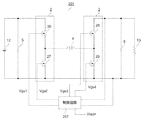
次に、本願発明の実施の形態1の昇降圧DC/DCコンバータ1に係るシステム構成について、図3に基づいて説明する。
昇降圧DC/DCコンバータ1の主回路の入力側である降圧回路2の入力には、交流発電機8の出力が整流器9を介して接続されている。昇降圧DC/DCコンバータ1の主回路の出力側である昇圧回路3の出力には、蓄電デバイスであるバッテリ10と負荷11が接続されている。
降圧回路2は、降圧スイッチング素子26と降圧同期整流スイッチング素子27から構成される。昇圧回路3は、昇圧スイッチング素子29と昇圧同期整流スイッチング素子28から構成される。
本実施の形態1の昇降圧DC/DCコンバータ1に係るシステムは、交流発電機8によって発電された電力をバッテリ10と負荷11に供給するもので、昇降圧DC/DCコンバータ1の入力電圧すなわち交流発電機8の出力電圧を調節することにより、交流発電機8の出力電力を調節するものである。
Next, a system configuration according to the step-up / step-down DC /
The output of the AC generator 8 is connected via a
The step-down
The system related to the step-up / step-down DC /
ここで交流発電機8は、図4に示す出力電圧−出力電力特性を持つものとする。図4の横軸が交流発電機8の出力電圧、縦軸が交流発電機8の出力電力であり、出力電圧0Vと開放電圧であるVoで出力電力0Wとなり、出力電圧Vpmaxで出力電力が最大のPmaxとなる垂下特性を持つものとする。すなわち、交流発電機8は、負荷の増加に伴い出力電圧が減少して出力電力が増加し、出力電圧Vpmaxで最大電力動作点の最大電力Pmaxとなり、さらに出力電圧を減少させると出力電力が減少する特性を有する。 Here, it is assumed that the AC generator 8 has the output voltage-output power characteristic shown in FIG. The horizontal axis of FIG. 4 is the output voltage of the AC generator 8, the vertical axis is the output power of the AC generator 8, the output voltage is 0V when the output voltage is 0V and the open voltage Vo, and the output power is maximum at the output voltage Vpmax. Suppose that it has the drooping characteristic which becomes Pmax. That is, in the AC generator 8, the output voltage decreases and the output power increases as the load increases, and becomes the maximum power Pmax at the maximum power operating point at the output voltage Vpmax, and the output power decreases when the output voltage is further decreased. It has the characteristic to do.
本実施の形態1では、昇降圧DC/DCコンバータ1の入力電圧が、交流発電機8の最大電力動作点であるVpmaxより低い電圧で制御される場合を想定しており、交流発電機8のVpmaxは、昇降圧DC/DCコンバータ1の出力電圧の目標値Vout*の2倍の電圧より高い電圧とする。
In the first embodiment, it is assumed that the input voltage of the step-up / step-down DC /
次に、図5に交流発電機8の出力電圧を0Vから昇降圧DC/DCコンバータ1の出力電圧の2倍まで調節できる昇降圧DC/DCコンバータ1の制御回路7のブロック図を示す。
図5の制御回路7の構成および動作概要を、図2で説明した制御回路基本構成と対比して説明する。
現在の電力変換状態を表す信号である昇降圧DC/DCコンバータ1の出力電圧Voutと、この信号の目標値であるVout*が、この発明における比較器21に対応する減算器31に入力されている。減算器31の出力が、この発明における第1制御器22に対応するPI制御器32で処理され、降圧回路2と昇圧回路3の両方のオンデューティを算出でき、両方同時にスイッチングすることがない関数Vpiを生成する。
この関数Vpiから、この発明における第2制御器23に対応する降圧デューティリミッタ33と降圧デューティ演算器34で、降圧回路2のオンデューティVbuckが算出される。また、関数Vpiから、この発明における第3制御器24に対応する昇圧デューティリミッタ40と昇圧デューティ演算器41で、昇圧回路3のオンデューティVboostが算出される。
なお、降圧デューティリミッタと昇圧デューティリミッタをまとめていうときは、デューティリミッタと記載する。
Next, FIG. 5 shows a block diagram of the
The configuration and operation outline of the
The output voltage Vout of the step-up / step-down DC /
From this function Vpi, the step-
The step-down duty limiter and the step-up duty limiter are collectively referred to as a duty limiter.
降圧デューティ演算器34の出力であるVbuckとキャリア波発生器35からのキャリア波Vcを用いて、コンパレータ36、遅延回路37、AND回路38およびNOR回路39が降圧回路2の降圧スイッチング素子26および降圧同期整流スイッチング素子27を制御する信号Vgs1およびVgs2を生成する。
The
さらに、図5の制御回路7の動作について詳細に説明する。
なお、以下の実施の形態1の説明では、関数Vpiをより具体的な制御電圧Vpiと記載する。
図3における降圧スイッチング素子26と降圧同期整流スイッチング素子27を駆動するゲート信号Vgs1およびVgs2は、図5の降圧デューティリミッタ33、降圧デューティ演算器34、キャリア波発生器35、コンパレータ36、遅延回路37、AND回路38およびNOR回路39を通して生成される。
なお、この発明における降圧回路2の降圧スイッチング素子26と降圧同期整流スイッチング素子27を駆動する駆動回路は、キャリア波発生器35、コンパレータ36、遅延回路37、AND回路38およびNOR回路39が対応する。
Further, the operation of the
In the following description of the first embodiment, the function Vpi is described as a more specific control voltage Vpi.
The gate signals Vgs1 and Vgs2 for driving the step-down
The drive circuit for driving the step-down
PI制御器32の出力である制御電圧Vpiは降圧デューティリミッタ33に入力され、降圧デューティリミッタ33では、制御電圧Vpiの最大値を2Vout*、最小値をVout*に制限する。これにより、降圧回路2のオンデューティVbuckの最大値を1、最小値を0.5とすることができる。
降圧デューティリミッタ33の出力は、降圧デューティ演算器34に入力される。降圧デューティ演算器34の計算式は、制御電圧Vpiを入力電圧と考えると一般的降圧DC/DCコンバータのオンデューティと入出力電圧の関係式(Vbuck=Vout*/Vpi)になっており、降圧回路2のオンデューティVbuckを求めることができる。
The control voltage Vpi, which is the output of the
The output of the step-
Vbuckとキャリア波発生器35からのキャリア波Vcを、コンパレータ36で比較して方形波を出力し、その方形波を遅延回路37、AND回路38およびNOR回路39を通して、デッドタイム付きの相補の信号Vgs1とVgs2が生成される。Vgs1が降圧スイッチング素子26を駆動するゲート信号となり、Vgs2が降圧同期整流スイッチング素子27を駆動するゲート信号となる。
Comparing Vback and the carrier wave Vc from the
図6に降圧回路2のオンデューティVbuck、キャリア波Vc、方形波V1、V2、ゲート信号Vgs1、Vgs2の関係を示す。
まず、降圧回路2のオンデューティVbuckとキャリア波Vcの大小関係から、方形波V1を出力する。そして、方形波V1を遅延回路37で時間tdだけ遅らせて、方形波V2を出力する。この方形波V1とV2をAND回路38に入力してVgs1、NOR回路39に入力してVgs2を生成する。
この方法は、デッドタイムを作成するひとつの方法であり、別の方法を用いてもよい。
FIG. 6 shows a relationship among the on-duty Vback, the carrier wave Vc, the square waves V1 and V2, and the gate signals Vgs1 and Vgs2 of the step-down
First, the square wave V1 is output from the magnitude relationship between the on-duty Vback of the step-down
This method is one method for creating dead time, and another method may be used.
図3における昇圧スイッチング素子29と昇圧同期整流スイッチング素子28を駆動するゲート信号Vgs4およびVgs3は、図5の昇圧デューティリミッタ40、昇圧デューティ演算器41、キャリア波発生器42、コンパレータ43、遅延回路44、AND回路45およびNOR回路46を通して生成される。
なお、この発明における昇圧回路3の昇圧スイッチング素子29と昇圧同期整流スイッチング素子28を駆動する駆動回路は、キャリア波発生器42、コンパレータ43、遅延回路44、AND回路45およびNOR回路46が対応する。
The gate signals Vgs4 and Vgs3 for driving the
Note that the
PI制御器32の出力である制御電圧Vpiは昇圧デューティリミッタ40に入力される。昇圧デューティリミッタ40は最大値をVout*、最小値を0と制限する。これにより、昇圧回路3のオンデューティVboostの最大値を1、最小値を0とすることができる。
昇圧デューティリミッタ40の出力は、昇圧デューティ演算器41に入力される。昇圧デューティ演算器41の計算式は、制御電圧Vpiを入力電圧と考えると、一般的昇圧DC/DCコンバータのオンデューティと入出力電圧の関係式(Vboost=1−Vpi/Vout*)になっており、昇圧回路3のオンデューティVboostを求めることができる。
The control voltage Vpi that is the output of the
The output of the
Vboostとキャリア波発生器42からのキャリア波Vcを、コンパレータ43で比較して方形波を出力する。その方形波を遅延回路44、AND回路45およびNOR回路46を通して、デッドタイムつきの相補の信号Vgs4とVgs3が生成される。
Vgs4が昇圧スイッチング素子29を駆動するゲート信号となり、Vgs3が昇圧同期整流スイッチング素子28を駆動するゲート信号となる。
A
Vgs4 becomes a gate signal for driving the step-up switching
図7に昇圧回路3のオンデューティVboost、キャリア波Vc、方形波V3、V4、ゲート信号Vgs4、Vgs3の関係を示す。
昇圧回路3のオンデューティVboostからゲート信号Vgs4、Vgs3を生成する方法は、図6と同様であるため、説明は省略する。
FIG. 7 shows a relationship among the on-duty Vboost, the carrier wave Vc, the square waves V3 and V4, and the gate signals Vgs4 and Vgs3 of the booster circuit 3.
The method for generating the gate signals Vgs4 and Vgs3 from the on-duty Vboost of the booster circuit 3 is the same as in FIG.
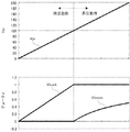
次に、制御電圧Vpiの変化に対する昇降圧DC/DCコンバータ1の降圧、昇圧動作の関係を、図8を用いて説明する。
図8は、出力電圧の目標値Vout*が、100のときの制御電圧Vpiと降圧回路2のオンデューティVbuckおよび昇圧回路3のオンデューティVboostの関係を示す。
制御電圧Vpiが100より小さいときは、Vbuckは1であり、Vboostは0より大きく1より小さい値を取り、昇圧動作を行う。制御電圧Vpiが100より大きいときは、Vboostは0であり、Vbuckは0より大きく1より小さい値を取り、降圧動作を行う。
なお、制御電圧Vpiが0のときは、VbuckおよびVboostを両方同時に1となり、交流発電機8の出力を短絡させて、交流発電機8の出力電力を0Wまで調節できる。
Next, the relationship between the step-down / step-up / step-up operation of the step-up / step-down DC /
FIG. 8 shows the relationship between the control voltage Vpi, the on-duty Vback of the step-down
When the control voltage Vpi is smaller than 100, Vback is 1, Vboost takes a value larger than 0 and smaller than 1, and performs a boosting operation. When the control voltage Vpi is greater than 100, Vboost is 0, Vback takes a value greater than 0 and less than 1, and performs a step-down operation.
When the control voltage Vpi is 0, both Vback and Vboost are simultaneously 1 and the output of the AC generator 8 can be short-circuited to adjust the output power of the AC generator 8 to 0 W.
実施の形態1においては、昇降圧DC/DCコンバータ1の入力に交流発電機8を接続したが、交流発電機に限らず電流源であればよい。
昇降圧DC/DCコンバータ1の出力に接続したバッテリ10についても、電気2重層コンデンサなど電圧源であればよい。
昇降圧DC/DCコンバータについても、降圧するためのスイッチング素子と昇圧するためのスイッチング素子を備え、それらのデューティによって、入出力の比を連続的に変化させることができるものであればよい。
また、スイッチング素子はすべてMOSFET(Metal−Oxide−Semiconductor Field−Effect Transistor)を使用しているが、IGBT(Insulated Gate Bipolar Transistor )やSiC(Silicon Carbide)のMOSFETなど他のスイッチング素子でもよい。
In the first embodiment, the AC generator 8 is connected to the input of the step-up / step-down DC /
The
The step-up / step-down DC / DC converter may be any one that includes a switching element for stepping down and a switching element for stepping up and that can continuously change the input / output ratio according to their duty.
In addition, although all switching elements use MOSFETs (Metal-Oxide-Semiconductor Field-Effect Transistors), other switching elements such as IGBTs (Insulated Gate Bipolar Transistors) or SiC (Silicon Carbide) MOSFETs may be used.
実施の形態1においては、図3に示すように降圧回路2に降圧同期整流スイッチング素子27を使用し、昇圧回路3に昇圧同期整流スイッチング素子28を使用する構成としたが、この降圧同期整流スイッチング素子27および昇圧同期整流スイッチング素子28は必ずしも必要ではない。これらの降圧、昇圧同期整流スイッチング素子を使用すると昇降圧DC/DCコンバータの変換効率は向上するが、これらの降圧、昇圧同期整流スイッチング素子を削除することで、制御回路を含めた昇降圧DC/DCコンバータの回路構成を簡素化することができる。
In the first embodiment, the step-down synchronous
実施の形態1においては、出力電圧とその目標値の偏差からPI制御で制御電圧Vpiを生成したが、制御電圧Vpiすなわち関数Vpiの生成方法は、これに限らない。例えば、PI制御に代えてPID制御を用いることができる。また、主回路の入力電圧や主回路内の電流とその目標値の偏差を用いて、関数Vpiを生成することができる。
また、交流発電機のVpmaxに追従するように、主回路内の電圧電流より交流発電機の出力電力を求め、現在の出力電圧と一定時間前の出力電圧を比較して、その大小関係により制御電圧Vpiを変化させる方法など、制御電圧Vpiを変化させて要求される発電状態にする方法を用いることができる。
In the first embodiment, the control voltage Vpi is generated by the PI control from the deviation between the output voltage and the target value. However, the method of generating the control voltage Vpi, that is, the function Vpi is not limited to this. For example, PID control can be used instead of PI control. Further, the function Vpi can be generated by using the input voltage of the main circuit or the current in the main circuit and the deviation of the target value.
Also, the output power of the AC generator is obtained from the voltage and current in the main circuit so as to follow the Vpmax of the AC generator, the current output voltage is compared with the output voltage for a certain time, and the control is performed according to the magnitude relationship. A method of changing the control voltage Vpi to a required power generation state such as a method of changing the voltage Vpi can be used.
次に、実施の形態1における他の実施例として、上記で説明した交流発電機のVpmaxに制御電圧Vpiを追従する制御する方法について説明する。
図9に、MPPT(Maximum Power Point Tracking)法を適用して、交流発電機の出力電圧を0Vから昇降圧DC/DCコンバータの出力電圧の2倍まで調節できる昇降圧DC/DCコンバータの制御回路の制御フローチャートを示す。
この制御フローチャートは、昇降圧DC/DCコンバータの現在の出力電力Poutと一つ前の制御周期の出力電力Pout_1を比較して、制御電圧Vpiを出力電力Poutが大きくなるように動かして、昇降圧DC/DCコンバータの入力電圧Vinが交流発電機の最大電力点Vpmaxになるように制御するものである。
Next, as another example of the first embodiment, a method of controlling the control voltage Vpi so as to follow Vpmax of the AC generator described above will be described.
FIG. 9 shows a step-up / step-down DC / DC converter control circuit that can adjust the output voltage of the AC generator from 0V to twice the output voltage of the step-up / step-down DC / DC converter by applying the MPPT (Maximum Power Point Tracking) method. The control flowchart of is shown.
This control flowchart compares the current output power Pout of the step-up / step-down DC / DC converter with the output power Pout_1 of the previous control cycle, and moves the control voltage Vpi so that the output power Pout becomes larger. Control is performed so that the input voltage Vin of the DC / DC converter becomes the maximum power point Vpmax of the AC generator.
なお、以下の説明では、現在の制御周期の出力電力をPout、Poutの1制御周期前のPoutをPout_1と定義する。また、Vpi_upは、前回の制御周期で制御電圧Vpiを大きくした場合は1、小さくした場合は0とする。 In the following description, output power in the current control cycle is defined as Pout, and Pout one control cycle before Pout is defined as Pout_1. Vpi_up is set to 1 when the control voltage Vpi is increased in the previous control cycle, and is set to 0 when the control voltage Vpi is decreased.
まずステップS1で制御電圧Vpiの初期値として0を代入する。
ステップS2で出力電圧Vout、出力電流Ioutを取得する。
ステップS3で現在の制御周期での出力電力Poutを算出する。
ステップS4、ステップS5、ステップS6で制御電圧Vpiを大きくするか、もしくは小さくするかを判定する。
まず、ステップS4で現在の制御周期の出力電力Poutと1つ前の制御周期の出力電力Pout_1の大小を比較する。出力電力Poutの方が大きければ、制御電圧Vpiを前回と同じ方向に動かすためにステップS5に進む。
Pout_1の方が大きければ、制御電圧Vpiを前回と逆の方向に動かすためにステップS6に進む。
First, in step S1, 0 is substituted as the initial value of the control voltage Vpi.
In step S2, the output voltage Vout and the output current Iout are acquired.
In step S3, the output power Pout in the current control cycle is calculated.
In step S4, step S5, and step S6, it is determined whether to increase or decrease the control voltage Vpi.
First, in step S4, the output power Pout of the current control cycle is compared with the output power Pout_1 of the previous control cycle. If the output power Pout is larger, the process proceeds to step S5 in order to move the control voltage Vpi in the same direction as the previous time.
If Pout_1 is larger, the process proceeds to step S6 in order to move the control voltage Vpi in the direction opposite to the previous time.
ステップS5でVpi_up=1かどうかを判定する。
Vpi_up=1の場合は、制御電圧Vpiを大きくするためにステップS7に、Vpi_up=0の場合は、制御電圧Vpiを小さくするためにステップS9に進む。
ステップS7で制御電圧VpiをΔVpiだけ大きくする。
ステップS8で制御電圧Vpiを大きくしたので、Vpi_upに1を代入する。
ステップS9で制御電圧VpiをΔVpiだけ小さくする。
ステップS10で制御電圧Vpiを小さくしたので、Vpi_upに0を代入する。
In step S5, it is determined whether Vpi_up = 1.
When Vpi_up = 1, the process proceeds to step S7 to increase the control voltage Vpi, and when Vpi_up = 0, the process proceeds to step S9 to decrease the control voltage Vpi.
In step S7, the control voltage Vpi is increased by ΔVpi.
Since the control voltage Vpi is increased in step S8, 1 is substituted into Vpi_up.
In step S9, the control voltage Vpi is decreased by ΔVpi.
Since the control voltage Vpi is reduced in step S10, 0 is substituted for Vpi_up.
ステップS11でVbuckの演算をする。これは図5の降圧デューティ演算器34と同じ役割である。
ステップS12でVboostの演算をする。これは図5の昇圧デューティ演算器41と同じ役割である。
ステップS13で出力電力PoutをPout_1に代入して、前回の制御周期の出力電力を記憶する。
ステップS2からステップS13を繰り返すことにより、発電機の出力電圧すなわち昇降圧DC/DCコンバータの入力電圧Vinは、Vpmaxに収束する。
In step S11, Vback is calculated. This has the same role as the step-
In step S12, Vboost is calculated. This has the same role as the step-up
In step S13, the output power Pout is substituted for Pout_1, and the output power of the previous control cycle is stored.
By repeating step S2 to step S13, the output voltage of the generator, that is, the input voltage Vin of the step-up / step-down DC / DC converter converges to Vpmax.
なお、ゲート信号の生成方法は、図5で説明したようにVbuckとVboostをキャリア波Vcと比較して生成する。 As described above with reference to FIG. 5, the gate signal is generated by comparing Vback and Vboost with the carrier wave Vc.
以上説明したように、実施の形態1に係る昇降圧DC/DCコンバータは、入力に交流発電機と整流器を接続し、出力にバッテリと負荷を接続し、出力電圧と出力電圧の目標値を比較して、降圧回路と昇圧回路の両方のオンデューティを算出でき、両方同時にスイッチングすることがない関数を生成し、この関数から降圧回路のオンデューティと昇圧回路のオンデューティを算出する制御回路を備えているため、降圧動作と昇圧動作の切り替えの判定が不要となり、降圧動作と昇圧動作の境界で出力電圧が不安定にならないという効果を有する。
As described above, the step-up / step-down DC / DC converter according to
また、実施の形態1に係る昇降圧DC/DCコンバータでは、昇降圧DC/DCコンバータの入力電圧すなわち交流発電機の出力電圧を、0Vから出力電圧の目標値の1/2まで、交流発電機のVpmaxより低い電圧で動作させて、所望の直流電圧を負荷に供給することができる。
さらに、実施の形態1に係る昇降圧DC/DCコンバータは、装置の小型化および変換効率の向上による省エネルギー効果がある。
In the step-up / step-down DC / DC converter according to the first embodiment, the input voltage of the step-up / step-down DC / DC converter, that is, the output voltage of the AC generator is changed from 0 V to 1/2 of the target value of the output voltage. The desired DC voltage can be supplied to the load by operating at a voltage lower than Vpmax.
Furthermore, the step-up / step-down DC / DC converter according to the first embodiment has an energy saving effect by downsizing the device and improving the conversion efficiency.
実施の形態2.
実施の形態1では、昇降圧DC/DCコンバータの入力電圧を、交流発電機のVpmaxより低い電圧で動作させていたが、本実施の形態2では、昇降圧DC/DCコンバータの入力電圧をVpmaxより高い電圧で動作させることを想定しており、また、交流発電機の出力電圧を昇降圧DC/DCコンバータの出力電圧の2分の1から交流発電機の開放電圧まで調節できるようにしたものである。
In the first embodiment, the input voltage of the step-up / step-down DC / DC converter is operated at a voltage lower than Vpmax of the AC generator. However, in the second embodiment, the input voltage of the step-up / step-down DC / DC converter is set to Vpmax. It is assumed to operate at a higher voltage, and the output voltage of the AC generator can be adjusted from one-half of the output voltage of the buck-boost DC / DC converter to the open voltage of the AC generator. It is.
以下、本願発明の実施の形態2の構成、動作について、昇降圧DC/DCコンバータ101の制御回路107のブロック図である図10に基づいて、実施の形態1との差異を中心に説明する。
実施の形態2に係る昇降圧DC/DCコンバータ101のシステム構成図は、実施の形態1に係る昇降圧DC/DCコンバータのシステム構成図である図3と同じであるため、図は省略している。また、交流発電機の出力電圧−出力電力特性図も図4と同じである。
図10において、実施の形態1の昇降圧DC/DCコンバータの制御回路7のブロック図である図5と同一あるいは相当部分には、同一の符号を付している。
なお、実施の形態1と区別するため、実施の形態2では、昇降圧DC/DCコンバータ101および制御回路107とする。
Hereinafter, the configuration and operation of the second embodiment of the present invention will be described based on FIG. 10 which is a block diagram of the
The system configuration diagram of the step-up / step-down DC / DC converter 101 according to the second embodiment is the same as FIG. 3, which is the system configuration diagram of the step-up / step-down DC / DC converter according to the first embodiment. Yes. Also, the output voltage-output power characteristic diagram of the AC generator is the same as FIG.
10, the same reference numerals are given to the same or corresponding parts as those in FIG. 5 which is a block diagram of the
In order to distinguish from the first embodiment, in the second embodiment, the step-up / step-down DC / DC converter 101 and the
図10の制御回路107のブロック図において、図5のブロック図との差異は減算器51、降圧デューティリミッタ52および昇圧デューティリミッタ53である。
減算器51において、電圧出力Voutと出力電圧の目標値Vout*の正負が逆になっている。こうすることで、実施の形態1では、電圧出力Voutが出力電圧の目標値Vout*に達していない場合、昇降圧DC/DCコンバータの入力電圧を上げていたが、実施の形態2では、昇降圧DC/DCコンバータの入力電圧を下げるように制御電圧Vpiは変動する。
次に、降圧デューティリミッタ52、昇圧デューティリミッタ53の値が実施の形態1とは異なる。降圧デューティリミッタ52の最大値をVoにすることで、交流発電機8の出力電圧を交流発電機8の開放電圧Voまで調節することができる。
また、昇圧デューティリミッタ53の最小値をVout*/2にすることで、交流発電機8の出力電圧を昇降圧DC/DCコンバータ101の出力電圧の2分の1より小さくならないように制御できる。
In the block diagram of the
In the
Next, the values of the step-
Further, by setting the minimum value of the
以上説明したように、実施の形態2に係る昇降圧DC/DCコンバータでは、入力に交流発電機と整流器を接続し、出力にバッテリと負荷を接続し、出力電圧と出力電圧の目標値を比較して、降圧回路と昇圧回路の両方のオンデューティを算出でき、両方同時にスイッチングすることがない関数を生成し、この関数から降圧回路のオンデューティと昇圧回路のオンデューティを算出する制御回路を備えているため、降圧動作と昇圧動作の切り替えの判定が不要となり、降圧動作と昇圧動作の境界で出力電圧が不安定にならないという効果を有する。 As described above, in the step-up / step-down DC / DC converter according to the second embodiment, the AC generator and the rectifier are connected to the input, the battery and the load are connected to the output, and the output voltage and the target value of the output voltage are compared. It is possible to calculate the on-duty of both the step-down circuit and the step-up circuit, generate a function that does not switch both at the same time, and have a control circuit that calculates the on-duty of the step-down circuit and the step-up circuit from this function Therefore, there is no need to determine switching between the step-down operation and the step-up operation, and the output voltage does not become unstable at the boundary between the step-down operation and the step-up operation.
また、実施の形態2に係る昇降圧DC/DCコンバータでは、昇降圧DC/DCコンバータの入力電圧すなわち交流発電機の出力電圧を、交流発電機の出力電圧を出力電圧の目標値の1/2から交流発電機の開放電圧Voまで交流発電機のVpmaxより高い電圧で動作させて、所望の直流電圧を負荷に供給することができる。 In the step-up / step-down DC / DC converter according to the second embodiment, the input voltage of the step-up / step-down DC / DC converter, that is, the output voltage of the AC generator, and the output voltage of the AC generator are ½ of the target value of the output voltage. To an open voltage Vo of the alternator can be operated at a voltage higher than Vpmax of the alternator to supply a desired DC voltage to the load.
実施の形態3.
実施の形態3は、入力にバッテリを接続し、出力に負荷を接続し、出力電圧と出力電圧の目標値を比較して、降圧回路と昇圧回路の両方のオンデューティを算出でき、両方同時にスイッチングすることがない関数を生成し、この関数から昇圧回路のオンデューティと降圧回路のオンデューティを算出する制御回路を備えた昇降圧DC/DCコンバータに関するものである。
Embodiment 3 FIG.
In the third embodiment, a battery is connected to the input, a load is connected to the output, the output voltage and the target value of the output voltage are compared, and the on-duty of both the step-down circuit and the step-up circuit can be calculated. The present invention relates to a step-up / step-down DC / DC converter having a control circuit that generates a function that does not occur and calculates an on-duty of a booster circuit and an on-duty of a step-down circuit from the function.
以下、本願発明の実施の形態3の構成、動作について、昇降圧DC/DCコンバータ201のシステム構成図である図11、制御回路207のブロック図である図12および動作説明図である図13に基づいて、実施の形態1との差異を中心に説明する。
図11において、図3と同一あるいは相当部分には、同一の符号を付している。また、図12において、図5と同一あるいは相当部分には、同一の符号を付している。
なお、実施の形態1と区別するため、実施の形態3では、昇降圧DC/DCコンバータ201および制御回路207とする。
Hereinafter, with respect to the configuration and operation of the third embodiment of the present invention, FIG. 11 is a system configuration diagram of the step-up / step-down DC /
In FIG. 11, the same or corresponding parts as in FIG. In FIG. 12, the same or corresponding parts as in FIG.
In order to distinguish from the first embodiment, in the third embodiment, the step-up / step-down DC /
本願発明の実施の形態3の昇降圧DC/DCコンバータ201に係るシステム構成について、図11に基づいて説明する。
昇降圧DC/DCコンバータ201の主回路の入力側である降圧回路2の入力には、蓄電デバイスであるバッテリ12が接続されている。昇降圧DC/DCコンバータ201の主回路の出力側である昇圧回路3の出力には、負荷13が接続されている。
本実施の形態3の昇降圧DC/DCコンバータ201に係るシステムは、バッテリ12の電圧を出力電圧の目標値Vout*に変換して、負荷13に供給するものである。
A system configuration relating to the step-up / step-down DC /
A
The system according to the step-up / step-down DC /
図12に、出力電圧を0Vからバッテリの電圧の2倍まで調節できる昇降圧DC/DCコンバータ201の制御回路207の制御ブロック図を示す。図5のブロック図との差異は、降圧デューティリミッタ61、降圧デューティ演算器62、昇圧デューティリミッタ63および昇圧デューティ演算器64である。降圧デューティ演算器62と昇圧デューティ演算器64の入力電圧の目標値Vin*は、ここではバッテリ12の定格電圧値とする。 制御電圧Vpiを出力電圧とすると、降圧デューティ演算器62の計算式は、一般的降圧DC/DCコンバータのオンデューティと入出力電圧の関係式(Vbuck=Vpi/Vin*)となる。
昇圧デューティ演算器64の計算式は、一般的昇圧DC/DCコンバータのオンデューティと入出力電圧の関係式(Vboost=1−Vin*/Vpi)となる。
また、降圧デューティリミッタ61で制御電圧Vpiの最小値を0にすることで、出力電圧を0Vまで降圧することができる。昇圧デューティリミッタ63では最大値を2Vin*にすることで、出力電圧をバッテリ12の電圧の2倍まで昇圧することができる。また、降圧スイッチング素子と昇圧スイッチング素子の両方のオンデューティが1となり、バッテリが短絡しないようになっている。
FIG. 12 is a control block diagram of the
The calculation formula of the step-up
Further, by setting the minimum value of the control voltage Vpi to 0 with the step-down duty limiter 61, the output voltage can be stepped down to 0V. The boosting
図13にVin*が100のときの制御電圧Vpiと降圧回路2のオンデューティVbuckおよび昇圧回路3のオンデューティVboostの関係を示す。
制御電圧Vpiが100より小さいときは、Vboostは0、Vbuckは0より大きく、1より小さい値を取り、降圧動作を行う。制御電圧Vpiが100より大きいときは、Vbuckは1、Vboostは0より大きく、1より小さい値を取り、昇圧動作を行う。
なお、VbuckおよびVboostは、制御電圧Vpiの取り得る範囲内において同時に1とならないため、入力に接続したバッテリ12を短絡させることはない。
また、制御電圧Vpiが0のときは、VbuckおよびVboostを両方同時に0となり、バッテリ12からの供給電力を0Wまで調節できる。
FIG. 13 shows the relationship between the control voltage Vpi when Vin * is 100, the on-duty Vback of the step-down
When the control voltage Vpi is smaller than 100, Vboost is 0, Vback is larger than 0 and smaller than 1, and the step-down operation is performed. When the control voltage Vpi is greater than 100, Vback is 1, Vboost is greater than 0 and less than 1, and the boost operation is performed.
Note that Vback and Vboost do not simultaneously become 1 within the range that the control voltage Vpi can take, so the
When the control voltage Vpi is 0, both Vback and Vboost are simultaneously 0, and the power supplied from the
実施の形態3においては、昇降圧DC/DCコンバータ201の入力にバッテリ12を接続したが、バッテリに限らず電気2重層コンデンサなど電圧源であればよい。
昇降圧DC/DCコンバータについても、降圧するためのスイッチング素子と昇圧するためのスイッチング素子を備え、それらのデューティによって、入出力の比を連続的に変化させることができるものであればよい。
また、スイッチング素子はすべてMOSFETを使用しているが、IGBTやSiCのMOSFETなど他のスイッチング素子でもよい。
In the third embodiment, the
The step-up / step-down DC / DC converter may be any one that includes a switching element for stepping down and a switching element for stepping up and that can continuously change the input / output ratio according to their duty.
Although all switching elements use MOSFETs, other switching elements such as IGBT and SiC MOSFETs may be used.
以上説明したように、実施の形態3に係る昇降圧DC/DCコンバータでは、入力にバッテリを接続し、出力に負荷を接続し、出力電圧と出力電圧の目標値を比較して、降圧回路と昇圧回路の両方のオンデューティを算出でき、両方同時にスイッチングすることがない関数を生成し、この関数から降圧回路のオンデューティと昇圧回路のオンデューティを算出する制御回路を備えているため、降圧動作と昇圧動作の切り替えの判定が不要となり、降圧動作と昇圧動作の境界で出力電圧が不安定にならないという効果を有する。 As described above, in the step-up / step-down DC / DC converter according to the third embodiment, the battery is connected to the input, the load is connected to the output, the output voltage and the target value of the output voltage are compared, Since it is possible to calculate the on-duty of both of the booster circuits and to generate a function that does not switch both at the same time, it has a control circuit that calculates the on-duty of the step-down circuit and the on-duty of the booster circuit from this function, so step-down operation Thus, there is no need to determine whether to switch the boost operation, and the output voltage does not become unstable at the boundary between the step-down operation and the boost operation.
また、実施の形態3に係る昇降圧DC/DCコンバータでは、昇降圧DC/DCコンバータの入力電圧すなわちバッテリの電圧を、0Vからバッテリの電圧の2倍の範囲内で所望の直流電圧に変換して負荷に供給することができる。 In the step-up / step-down DC / DC converter according to the third embodiment, the input voltage of the step-up / step-down DC / DC converter, that is, the battery voltage is converted into a desired DC voltage within a range of 0V to twice the battery voltage. Can be supplied to the load.
実施の形態4.
実施の形態3の昇降圧DC/DCコンバータは、出力電圧を0Vからバッテリの電圧の2倍まで調節できるようにしていたが、本実施の形態4では、バッテリの電圧を降圧する場合、5分の1以下の降圧比にはならないにしたものである。すなわち、昇降圧DC/DCコンバータの出力電圧を、バッテリの電圧の1/5から2倍に変換して、負荷に供給するようにしたものである。
The step-up / step-down DC / DC converter according to the third embodiment can adjust the output voltage from 0 V to twice the voltage of the battery, but in the fourth embodiment, when the voltage of the battery is stepped down, it is 5 minutes. The step-down ratio is not less than 1. That is, the output voltage of the step-up / step-down DC / DC converter is converted from 1/5 to twice the voltage of the battery and supplied to the load.
以下、本願発明の実施の形態4の構成、動作について、昇降圧DC/DCコンバータ301の制御回路307のブロック図である図14に基づいて、実施の形態3との差異を中心に説明する。
実施の形態4に係る昇降圧DC/DCコンバータ301のシステム構成図は、実施の形態3に係る昇降圧DC/DCコンバータ201のシステム構成図である図11と同じであるため、図は省略している。
図14において、実施の形態3の昇降圧DC/DCコンバータ201の制御回路207のブロック図である図11と同一あるいは相当部分には、同一の符号を付している。
なお、実施の形態3と区別するため、実施の形態4では、昇降圧DC/DCコンバータ301および制御回路307とする。
Hereinafter, the configuration and operation of the fourth embodiment of the present invention will be described based on FIG. 14 which is a block diagram of the
The system configuration diagram of the step-up / step-down DC / DC converter 301 according to the fourth embodiment is the same as FIG. 11, which is the system configuration diagram of the step-up / step-down DC /
In FIG. 14, the same reference numerals are given to the same or equivalent parts in FIG. 11 which is a block diagram of the
In order to distinguish from the third embodiment, in the fourth embodiment, the step-up / step-down DC / DC converter 301 and the
図14に、出力電圧をバッテリの電圧の5分の1からバッテリの電圧の2倍まで調節できる昇降圧DC/DCコンバータの制御回路の制御ブロック図を示す。図11のブロック図との差異は、降圧デューティリミッタ71の値である。
降圧デューティリミッタ71の最小値をVin*/5とすることで、昇降圧DC/DCコンバータ301の出力電圧をバッテリ12の電圧の5分の1より低くならないように制御できる。
FIG. 14 shows a control block diagram of a control circuit of the step-up / step-down DC / DC converter capable of adjusting the output voltage from one-fifth of the battery voltage to twice the battery voltage. The difference from the block diagram of FIG. 11 is the value of the step-
By setting Vin * / 5 as the minimum value of the step-
以上説明したように、実施の形態4に係る昇降圧DC/DCコンバータでは、入力にバッテリを接続し、出力に負荷を接続し、出力電圧と出力電圧の目標値を比較して、降圧回路と昇圧回路の両方のオンデューティを算出でき、両方同時にスイッチングすることがない関数を生成し、この関数から降圧回路のオンデューティと昇圧回路のオンデューティを算出する制御回路を備えているため、降圧動作と昇圧動作の切り替えの判定が不要となり、降圧動作と昇圧動作の境界で出力電圧が不安定にならないという効果を有する。 As described above, in the step-up / step-down DC / DC converter according to the fourth embodiment, the battery is connected to the input, the load is connected to the output, the output voltage and the target value of the output voltage are compared, Since it is possible to calculate the on-duty of both of the booster circuits and to generate a function that does not switch both at the same time, it has a control circuit that calculates the on-duty of the step-down circuit and the on-duty of the booster circuit from this function, so step-down operation Thus, there is no need to determine whether to switch the boost operation, and the output voltage does not become unstable at the boundary between the step-down operation and the boost operation.
また、実施の形態4に係る昇降圧DC/DCコンバータでは、昇降圧DC/DCコンバータの入力電圧すなわちバッテリの電圧を、バッテリの電圧の1/5から2倍の範囲内で所望の直流電圧に変換して負荷に供給することができる。 In the step-up / step-down DC / DC converter according to the fourth embodiment, the input voltage of the step-up / step-down DC / DC converter, that is, the voltage of the battery is changed to a desired DC voltage within a range of 1/5 to twice the battery voltage. It can be converted and supplied to the load.
なお、本発明は、その発明の範囲内において、各実施の形態を自由に組み合わせたり、各実施の形態を適宜、変形、省略したりすることが可能である。 It should be noted that the present invention can be freely combined with each other within the scope of the invention, and each embodiment can be appropriately modified or omitted.
1,101,201,301 昇降圧DC/DCコンバータ、2 降圧回路、
3 昇圧回路、4 平滑リアクトル、5 入力平滑コンデンサ、
6 出力平滑コンデンサ、7,107,207,307 制御回路、8 交流発電機、
9 整流器、10,12 バッテリ、11,13 負荷、21 比較器、
22 第1制御器、23 第2制御器、24 第3制御器、
26 降圧スイッチング素子、27 降圧同期整流スイッチング素子、
28 昇圧同期整流スイッチング素子、29 昇圧スイッチング素子、
31,51 減算器、32 PI制御器、
33,52,61,71 降圧デューティリミッタ、
34,62 降圧デューティ演算器、35,42 キャリア波発生器、
36,43 コンパレータ、37,44 遅延器、38,45 AND回路、
39,46 NOR回路、40,53,63 昇圧デューティリミッタ、
41,64 昇圧デューティ演算器。
1, 101, 201, 301 buck-boost DC / DC converter, 2 step-down circuit,
3 Booster circuit, 4 smoothing reactor, 5 input smoothing capacitor,
6 output smoothing capacitor, 7, 107, 207, 307 control circuit, 8 AC generator,
9 Rectifier, 10, 12 Battery, 11, 13 Load, 21 Comparator,
22 1st controller, 23 2nd controller, 24 3rd controller,
26 step-down switching element, 27 step-down synchronous rectification switching element,
28 step-up synchronous rectification switching element, 29 step-up switching element,
31, 51 subtractor, 32 PI controller,
33, 52, 61, 71 step-down duty limiter,
34,62 step-down duty calculator, 35,42 carrier wave generator,
36, 43 Comparator, 37, 44 Delay, 38, 45 AND circuit,
39, 46 NOR circuit, 40, 53, 63 step-up duty limiter,
41, 64 Boosting duty calculator.
Claims (14)
前記主回路の入力電圧、電流を取り込むとともに、前記入力電圧、電流の目標値を取り込み、および/または、前記主回路の出力電圧、電流を取り込むとともに、前記出力電圧、電流の目標値を取り込み、前記取り込んだ電圧、電流値から算出される現在の電力変換状態と前記取り込んだ電圧、電流値の目標値から算出される目標の電力変換状態とを比較する比較器と、
前記降圧回路のオンデューティと前記昇圧回路のオンデューティの両方のオンデューティを算出でき、前記降圧回路の降圧スイッチング素子と前記昇圧回路の昇圧スイッチング素子の両方が同時にスイッチングすることはない関数を生成する第1制御器と、
生成した前記関数から前記降圧回路のオンデューティを算出する第2制御器と、
生成した前記関数から前記昇圧回路のオンデューティを算出する第3制御器と、
前記降圧回路の降圧スイッチング素子と前記昇圧回路の昇圧スイッチング素子をスイッチング制御する制御回路とを備えた昇降圧DC/DCコンバータ。 A step-down circuit including a step-down switching element for stepping down an input voltage, a step-up circuit including a step-up switching element for stepping up the input voltage, a smoothing reactor connecting the step-down circuit and the step-up circuit, and an input of the step-down circuit A main circuit composed of an input smoothing capacitor provided on the output circuit and an output smoothing capacitor provided on the output of the booster circuit;
Taking in the input voltage and current of the main circuit, taking in the target value of the input voltage and current, and / or taking in the output voltage and current of the main circuit, and taking in the target value of the output voltage and current, A comparator that compares a current power conversion state calculated from the captured voltage and current value with a target power conversion state calculated from the target value of the captured voltage and current value;
Both the on-duty of the step-down circuit and the on-duty of the step-up circuit can be calculated, and a function is generated in which both the step-down switching element of the step-down circuit and the step-up switching element of the step-up circuit do not switch simultaneously. A first controller;
A second controller for calculating an on-duty of the step-down circuit from the generated function;
A third controller for calculating an on-duty of the booster circuit from the generated function;
A step-up / step-down DC / DC converter comprising a step-down switching element of the step-down circuit and a control circuit that controls switching of the step-up switching element of the step-up circuit.
Priority Applications (1)
| Application Number | Priority Date | Filing Date | Title |
|---|---|---|---|
| JP2012106489A JP2013236435A (en) | 2012-05-08 | 2012-05-08 | Buck/boost dc/dc converter |
Applications Claiming Priority (1)
| Application Number | Priority Date | Filing Date | Title |
|---|---|---|---|
| JP2012106489A JP2013236435A (en) | 2012-05-08 | 2012-05-08 | Buck/boost dc/dc converter |
Publications (2)
| Publication Number | Publication Date |
|---|---|
| JP2013236435A true JP2013236435A (en) | 2013-11-21 |
| JP2013236435A5 JP2013236435A5 (en) | 2014-12-04 |
Family
ID=49762113
Family Applications (1)
| Application Number | Title | Priority Date | Filing Date |
|---|---|---|---|
| JP2012106489A Pending JP2013236435A (en) | 2012-05-08 | 2012-05-08 | Buck/boost dc/dc converter |
Country Status (1)
| Country | Link |
|---|---|
| JP (1) | JP2013236435A (en) |
Cited By (6)
| Publication number | Priority date | Publication date | Assignee | Title |
|---|---|---|---|---|
| US9537423B2 (en) | 2012-09-24 | 2017-01-03 | General Electric Company | Power conversion system |
| WO2018038362A1 (en) * | 2016-08-22 | 2018-03-01 | 데스틴파워 주식회사 | Buck boost converter |
| JP2020096460A (en) * | 2018-12-13 | 2020-06-18 | 株式会社ダイヘン | Power converter |
| JP2020108316A (en) * | 2018-12-28 | 2020-07-09 | 株式会社ダイヘン | Power conversion apparatus |
| WO2020235323A1 (en) * | 2019-05-21 | 2020-11-26 | 株式会社オートネットワーク技術研究所 | Voltage conversion device |
| US10965206B2 (en) | 2017-03-13 | 2021-03-30 | Rohm Co., Ltd. | Step-up/down DC-DC converter |
Citations (3)
| Publication number | Priority date | Publication date | Assignee | Title |
|---|---|---|---|---|
| JPH11299229A (en) * | 1998-04-08 | 1999-10-29 | Toyota Autom Loom Works Ltd | Power circuit |
| JP2003070296A (en) * | 2001-08-24 | 2003-03-07 | Toa Electric Industry Co Ltd | Maximum power acquisition control method of wind power equipment |
| JP2009183080A (en) * | 2008-01-31 | 2009-08-13 | Nissan Motor Co Ltd | Controller for dc-dc converter |
-
2012
- 2012-05-08 JP JP2012106489A patent/JP2013236435A/en active Pending
Patent Citations (3)
| Publication number | Priority date | Publication date | Assignee | Title |
|---|---|---|---|---|
| JPH11299229A (en) * | 1998-04-08 | 1999-10-29 | Toyota Autom Loom Works Ltd | Power circuit |
| JP2003070296A (en) * | 2001-08-24 | 2003-03-07 | Toa Electric Industry Co Ltd | Maximum power acquisition control method of wind power equipment |
| JP2009183080A (en) * | 2008-01-31 | 2009-08-13 | Nissan Motor Co Ltd | Controller for dc-dc converter |
Cited By (11)
| Publication number | Priority date | Publication date | Assignee | Title |
|---|---|---|---|---|
| US9537423B2 (en) | 2012-09-24 | 2017-01-03 | General Electric Company | Power conversion system |
| WO2018038362A1 (en) * | 2016-08-22 | 2018-03-01 | 데스틴파워 주식회사 | Buck boost converter |
| US10658930B2 (en) | 2016-08-22 | 2020-05-19 | Destinpower Inc. | Buck boost converter |
| US10965206B2 (en) | 2017-03-13 | 2021-03-30 | Rohm Co., Ltd. | Step-up/down DC-DC converter |
| JP2020096460A (en) * | 2018-12-13 | 2020-06-18 | 株式会社ダイヘン | Power converter |
| JP2020108316A (en) * | 2018-12-28 | 2020-07-09 | 株式会社ダイヘン | Power conversion apparatus |
| JP7305348B2 (en) | 2018-12-28 | 2023-07-10 | 株式会社ダイヘン | power converter |
| WO2020235323A1 (en) * | 2019-05-21 | 2020-11-26 | 株式会社オートネットワーク技術研究所 | Voltage conversion device |
| JP2020191714A (en) * | 2019-05-21 | 2020-11-26 | 株式会社オートネットワーク技術研究所 | Voltage converter |
| JP7100810B2 (en) | 2019-05-21 | 2022-07-14 | 株式会社オートネットワーク技術研究所 | Voltage converter |
| US11881781B2 (en) | 2019-05-21 | 2024-01-23 | Autonetworks Technologies, Ltd. | Voltage conversion device |
Similar Documents
| Publication | Publication Date | Title |
|---|---|---|
| JP6569839B1 (en) | Power converter | |
| US20140369090A1 (en) | Inverter apparatus | |
| JP6150018B2 (en) | DC-DC converter, power converter, power generation system, and DC-DC conversion method | |
| JP5349688B2 (en) | Grid-connected inverter | |
| JP2013236435A (en) | Buck/boost dc/dc converter | |
| JP2006238628A (en) | Power converting device | |
| JP6185860B2 (en) | Bidirectional converter | |
| TWI694668B (en) | DC-DC converter and power conditioner | |
| Ahmed | Modeling and simulation of ac–dc buck-boost converter fed dc motor with uniform PWM technique | |
| JP2017060303A (en) | Power supply device | |
| JP6190979B2 (en) | DC / DC converter | |
| WO2011135657A1 (en) | System interconnection inverter | |
| JP5716631B2 (en) | Power converter | |
| US10263534B2 (en) | Power conversion device | |
| JP2013236435A5 (en) | ||
| JP2015228728A (en) | Converter | |
| Ma et al. | Improved asynchronous voltage regulation strategy of non-inverting Buck-Boost converter for renewable energy integration | |
| JP5638462B2 (en) | Buck-boost bidirectional DC / DC converter and AC motor drive device using the same | |
| JP5924281B2 (en) | Power conversion apparatus and grid interconnection system | |
| JP6106568B2 (en) | Power converter | |
| KR101469354B1 (en) | Inverter apparatus and photovoltaic power generation system | |
| Wei et al. | Efficiency-Oriented Optimized Design and Control of Hybrid FSBB-CLLC Converters with Partial Power Processing Capability | |
| Doubabi et al. | Modeling and design of synchronous buck converter for solar-powered refrigerator | |
| JP5703524B2 (en) | Power supply unit | |
| JP6197700B2 (en) | Power converter |
Legal Events
| Date | Code | Title | Description |
|---|---|---|---|
| A521 | Written amendment |
Free format text: JAPANESE INTERMEDIATE CODE: A523 Effective date: 20141017 |
|
| A621 | Written request for application examination |
Free format text: JAPANESE INTERMEDIATE CODE: A621 Effective date: 20141017 |
|
| A977 | Report on retrieval |
Free format text: JAPANESE INTERMEDIATE CODE: A971007 Effective date: 20150928 |
|
| A131 | Notification of reasons for refusal |
Free format text: JAPANESE INTERMEDIATE CODE: A131 Effective date: 20150929 |
|
| A02 | Decision of refusal |
Free format text: JAPANESE INTERMEDIATE CODE: A02 Effective date: 20160216 |