JP5493902B2 - Power converter - Google Patents
Power converter Download PDFInfo
- Publication number
- JP5493902B2 JP5493902B2 JP2010010230A JP2010010230A JP5493902B2 JP 5493902 B2 JP5493902 B2 JP 5493902B2 JP 2010010230 A JP2010010230 A JP 2010010230A JP 2010010230 A JP2010010230 A JP 2010010230A JP 5493902 B2 JP5493902 B2 JP 5493902B2
- Authority
- JP
- Japan
- Prior art keywords
- power
- point
- capacitor
- semiconductor switching
- switching element
- Prior art date
- Legal status (The legal status is an assumption and is not a legal conclusion. Google has not performed a legal analysis and makes no representation as to the accuracy of the status listed.)
- Expired - Fee Related
Links
Images


Classifications
-
- H—ELECTRICITY
- H02—GENERATION; CONVERSION OR DISTRIBUTION OF ELECTRIC POWER
- H02M—APPARATUS FOR CONVERSION BETWEEN AC AND AC, BETWEEN AC AND DC, OR BETWEEN DC AND DC, AND FOR USE WITH MAINS OR SIMILAR POWER SUPPLY SYSTEMS; CONVERSION OF DC OR AC INPUT POWER INTO SURGE OUTPUT POWER; CONTROL OR REGULATION THEREOF
- H02M7/00—Conversion of ac power input into dc power output; Conversion of dc power input into ac power output
- H02M7/02—Conversion of ac power input into dc power output without possibility of reversal
- H02M7/04—Conversion of ac power input into dc power output without possibility of reversal by static converters
- H02M7/12—Conversion of ac power input into dc power output without possibility of reversal by static converters using discharge tubes with control electrode or semiconductor devices with control electrode
- H02M7/21—Conversion of ac power input into dc power output without possibility of reversal by static converters using discharge tubes with control electrode or semiconductor devices with control electrode using devices of a triode or transistor type requiring continuous application of a control signal
- H02M7/217—Conversion of ac power input into dc power output without possibility of reversal by static converters using discharge tubes with control electrode or semiconductor devices with control electrode using devices of a triode or transistor type requiring continuous application of a control signal using semiconductor devices only
-
- H—ELECTRICITY
- H02—GENERATION; CONVERSION OR DISTRIBUTION OF ELECTRIC POWER
- H02M—APPARATUS FOR CONVERSION BETWEEN AC AND AC, BETWEEN AC AND DC, OR BETWEEN DC AND DC, AND FOR USE WITH MAINS OR SIMILAR POWER SUPPLY SYSTEMS; CONVERSION OF DC OR AC INPUT POWER INTO SURGE OUTPUT POWER; CONTROL OR REGULATION THEREOF
- H02M1/00—Details of apparatus for conversion
- H02M1/0083—Converters characterised by their input or output configuration
- H02M1/0085—Partially controlled bridges
-
- H—ELECTRICITY
- H02—GENERATION; CONVERSION OR DISTRIBUTION OF ELECTRIC POWER
- H02M—APPARATUS FOR CONVERSION BETWEEN AC AND AC, BETWEEN AC AND DC, OR BETWEEN DC AND DC, AND FOR USE WITH MAINS OR SIMILAR POWER SUPPLY SYSTEMS; CONVERSION OF DC OR AC INPUT POWER INTO SURGE OUTPUT POWER; CONTROL OR REGULATION THEREOF
- H02M1/00—Details of apparatus for conversion
- H02M1/12—Arrangements for reducing harmonics from ac input or output
- H02M1/123—Suppression of common mode voltage or current
Landscapes
- Engineering & Computer Science (AREA)
- Power Engineering (AREA)
- Rectifiers (AREA)
- Inverter Devices (AREA)
- Power Conversion In General (AREA)
Description
本発明は、半導体スイッチング素子を用いた電力変換装置に関する。 The present invention relates to a power conversion device using a semiconductor switching element.
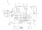
この種の電力変換装置としては、例えば、図8に示す構成が知られている。
この図8に示す電力変換装置は、単相の交流電源101と、この交流電源101の交流出力電力を直流電力に変換する整流回路102と、この整流回路102の正極側ラインLp及び負極側ラインLnから出力される直流電力を平滑化する平滑用コンデンサ103と、正極側ラインLp及び負極側ラインLn間に接続された直流負荷104とを備えている。
For example, a configuration shown in FIG. 8 is known as this type of power conversion device.
The power conversion apparatus shown in FIG. 8 includes a single-phase
整流回路102は、正極側ラインLp及び負極側ラインLn間に、整流素子としてのダイオード105a,105bと例えば半導体スイッチング素子としてのMOSFET106a,106bとをそれぞれ直列に接続した直列回路107及び108が並列に接続された構成を有する。ここで、MOSFET106a及び106bの夫々は、内部に寄生ダイオードを持つため、逆方向電流に対してはゲート電圧にかかわらず常に導通状態となる。
In the
そして、各直列回路105及び106のダイオード105a及び105bとMOSFET106a及び106bとの接続点でなる交流入力点Pia及びPibがそれぞれリアクトル109a及び109bを介して交流電源101に接続されている。
また、交流電源101の出力側とリアクトル109a及び109bとを結ぶ電源ラインLa及びLb間に、ノイズフィルタを構成する接地コンデンサ110a及び110bの直列回路が接続され、これら接地コンデンサ110a及び110bの接続点が大地電位Gに接続されている。
Then, AC input points Pia and Pib, which are connection points between the
A series circuit of
この図8に示す電力変換装置では、整流回路102に入力される交流電源101の交流入力電流Iinを、交流入力電圧Vinと位相の等しい正弦波波形としつつ、直流出力電圧Edを交流入力電圧Vinのピーク値より高い所望の値に保つ機能を有する。
これらの機能を実現するための動作を以下に説明する。
例えば交流入力電圧Vinが正極性の場合、MOSFET106aをオン状態とすると、交流電源101から電源ラインLa、リアクトル109a、MOSFET106a、MOSFET106b、リアクトル109b、電源ラインLbを介して交流電源101に戻る経路で電流が流れる。このため、交流電源101の電圧がリアクトル109a及び109bに1/2ずつかかり交流入力電流Iinは増加する。
In the power conversion device shown in FIG. 8, the AC input current Iin of the
The operation for realizing these functions will be described below.
For example, when the AC input voltage Vin is positive, when the
この状態でMOSFET106aをオフ状態とすると、交流電源101から電源ラインLa、リアクトル109a、ダイオード105a、平滑用コンデンサ103、MOSFET106b、リアクトル109b、電源ラインLbを介して交流電源101に戻る経路で電流が流れる。このとき、リアクトル109a及び109bには、直流出力電圧Edと交流入力電圧Vinとの差電圧が1/2ずつ印加されるが、回路の動作により、直流出力電圧Edは交流入力電圧Vinのピーク値より高く保たれているので、交流入力電流Iinは減少する。
When the
したがって、MOSFET106aのオンとオフの時比率すなわちデューティ比を制御することにより、交流入力電流Iinの波形と大きさを任意に制御できる。これにより交流入力電流Iinの波形を正弦波(ここではリップル分は無視する)とし、また、負荷電力に応じて交流入力電流Iinの振幅を制御することで直流出力電圧Edを所望の値に保つ。
Therefore, the waveform and magnitude of the AC input current Iin can be arbitrarily controlled by controlling the ON / OFF time ratio of the
交流入力電圧Vinが負極性の場合は、MOSFET106bのオン・オフ動作により同様の動作を行う。ここで、交流入力電圧Vinが正(MOSFET106aがオン・オフ動作)の際はMOSFET106bが、交流入力電圧Vinが負(MOSFET106bがオン・オフ動作)の際はMOSFET106aがそれぞれゲート信号に関わらず逆方向導通状態となる。
When the AC input voltage Vin is negative, the same operation is performed by turning on and off the
一般に、このようなスイッチングによる電力変換装置は、スイッチングの度に電位の変動があり、それに起因するノイズを発生する。このノイズは、ノイズフィルタとしての接地コンデンサ110a及び110bによって外部に流出することが防止される。ここで、交流入力電圧Vinの中性点電位を大地電位Gとすると、接地コンデンサ110a及び110bの電圧はそれぞれVin/2となる。スイッチングに伴う各点の大地電位Gに対する電位の変化を図9に示す。MOSFET106a及び106bがオン状態となっているタイミングでは、接地コンデンサ110a及び110bの両端のU点及びV点間が短絡され、前述したようにリアクトル109a及び109bの両端電圧VL1及びVL2はVL1=VL2=Vin/2となる。ここで、U点電位は+Vin/2、V点電位は−Vin/2であるので、交流入力点Pia及びPibの電位は0Vとなる。この電位はMOSFET106a及び106bが導通しているので、平滑用コンデンサ103の負側のN点電位とも等しいため、N点電位は0V、平滑用コンデンサ103の正側のP点電位はN点電位+直流出力電圧Edであるため直流出力電圧Edとなる。
In general, such a power conversion apparatus using switching has a potential change every time switching is performed, and generates noise due to the fluctuation. This noise is prevented from flowing out by the
一方、交流入力電圧Vinが正でMOSFET106aがオフしたタイミングでは交流入力点Piaの電位はP点電位と、交流入力点Pibの電位はN点電位とそれぞれ等しくなる。このため、接地コンデンサ110a,110bの両端のU−V間には直流出力電圧Edが印加されるので、VL1=VL2=(Vin−Ed)/2となる。したがって、Pia点電位(=P点電位)はVin/2−(Vin−Ed)/2=+Ed/2となり、Pib点電位は−Vin/2+(Vin−Ed)/2=−Ed/2となる。すなわち、Pia点の電位は+Ed/2変動し、Pib点、P点及びN点の電位は−Ed/2変動する。
On the other hand, at the timing when the AC input voltage Vin is positive and the
交流入力電圧Vinが負でMOSFET106bがオフしたタイミングでは同様の動作により、Pib点の電位が+Ed/2変動し、Pia点、P点及びN点の電位は−Ed/2変動する。また、MOSFET106a及び106bが再びオン状態となると、逆向きの電位変動が発生する。
ところで、図8に示す従来例にあっては、各点と装置のフレームFG間には意図しない寄生キャパシタンス111〜114が存在する。フレームFGは安全上の理由により接地されるため、寄生キャパシタンス111〜114は対地キャパシタンスとして作用する。上述の電位変動により各々の寄生キャパシタンスに電流が流れ、これらが接地コンデンサ110a及び110bを介して図8に示す電流Ieが回路内を循環する。この際、接地コンデンサ110a及び110bには高周波の電圧、所謂雑音端子電圧が発生する。
At the timing when the AC input voltage Vin is negative and the
Incidentally, in the conventional example shown in FIG. 8, unintended parasitic capacitances 111 to 114 exist between each point and the frame FG of the apparatus. Since the frame FG is grounded for safety reasons, the parasitic capacitances 111 to 114 act as ground capacitances. Due to the above-described potential fluctuation, a current flows through each parasitic capacitance, and the current Ie shown in FIG. 8 circulates in the circuit via the
この雑音端子電圧は、交流電源101に接続される他の機器に悪影響を与えないように制限する必要がある。最も単純な方法は、接地コンデンサ110a及び110bのキャパシタンスを大きくすることであるが、これらは高周波電流だけではなく、交流入力電圧Vinによる低周波電流も漏洩電流として流すため、キャパシタンスが大きすぎると漏電ブレーカのトリップ等を引き起こす等の問題を生じる。その他、良く知られた方法としては、装置と電源の間にコモンモードチョークコイルを介挿するものがあるが、コモンモードチョークコイルは主回路電流を流す都合上、外形が大きなものになることを避けることができない。このため、電力変換装置の小形化の妨げとなり、さらにはコスト増加の要因となる。
This noise terminal voltage needs to be limited so as not to adversely affect other devices connected to the
これに対して、スイッチング手段を用いたノイズ抑制方法としては、例えばノイズ検出手段で検出されたノイズ電流に対し、これと逆向きの電流を発生するスイッチ素子からなる電流供給回路を平滑用コンデンサに接続されたエネルギー回生用トランスを用いた電圧クランプ回路と大地電位G間に接続して、ノイズを抑制するノイズ低減装置が知られている(例えば、特許文献1参照)。 On the other hand, as a noise suppression method using switching means, for example, a current supply circuit comprising a switching element that generates a current in the opposite direction to the noise current detected by the noise detection means is used as a smoothing capacitor. A noise reduction device that suppresses noise by connecting between a voltage clamp circuit using a connected energy regeneration transformer and a ground potential G is known (for example, see Patent Document 1).
また、他のノイズ抑制方法としては、インバータやモータジェネレータを含む高圧系部品と車両アースとの間の固有の浮遊容量と直列に静電容量を接続し、この静電容量と並列に接続スイッチを接続し、この接続スイッチを、負荷を駆動する際にオン状態とし、非駆動状態でオフ状態に制御する電動車両が知られている(例えば、特許文献2参照)。 As another noise suppression method, a capacitance is connected in series with the inherent stray capacitance between the high-voltage system parts including the inverter and motor generator and the vehicle ground, and a connection switch is connected in parallel with this capacitance. 2. Description of the Related Art There is known an electric vehicle that is connected, and this connection switch is turned on when driving a load and is controlled to be turned off in a non-driven state (see, for example, Patent Document 2).
しかしながら、上記特許文献1に記載された従来例にあっては、ノイズをキャンセルするための電流をスイッチング手段自らが作り出す必要があるため、スイッチング手段は極めて高速のものである必要があり、同時に高速の制御を必要とする上、構成が複雑となるという未解決の課題がある。
また、上記特許文献2に記載された従来例にあっては、装置全体の外部との接続状態に応じて対地キャパシタンスを変えて、装置の電位変動と漏洩電流の大小を調整するものであって、装置全体の外部との接続状態が一定である場合には適用することができず、さらにノイズ源となる装置が動作している際の漏洩電流を減らすことができないという未解決の課題がある。
そこで、本発明は、上述した従来例の未解決の課題に着目してなされたものであり、体積的な課題とコスト的な課題を同時に解消しつつ雑音端子電圧を低減することができる電力変換装置を提供することを目的としている。
However, in the conventional example described in Patent Document 1, since it is necessary for the switching means itself to generate a current for canceling the noise, the switching means needs to be extremely fast, and at the same time, high speed. However, there is an unsolved problem that the configuration becomes complicated.
Further, in the conventional example described in
Therefore, the present invention has been made paying attention to the above-mentioned unsolved problems of the conventional example, and power conversion that can reduce the noise terminal voltage while simultaneously solving the volume problem and the cost problem. The object is to provide a device.
上記目的を達成するために、本発明の一の形態に係る電力変換装置は、交流電源と、該交流電源から入力される交流電力を直流電力に変換する整流回路とを有し、前記整流回路は、整流素子と半導体スイッチング素子とを直列に接続した直列回路を正極側ライン及び負極側ライン間に入力交流の相数分並列に接続した構成を有し、各直列回路の前記整流素子及び半導体スイッチング素子の接続点でなる交流入力点に前記交流電源がインダクタンス素子を介して接続された電力変換装置であって、前記各直列回路の前記交流入力点のそれぞれと、大地電位となる点との間をスイッチ手段及びコンデンサを直列に接続したノイズ抑制直列回路を介して接続し、前記ノイズ抑制直列回路は、前記スイッチ手段と並列に接続された抵抗を有し、該抵抗の抵抗値を、前記コンデンサが前記交流入力点の交流入力電力の周波数に対して示すインピーダンスよりも十分小さく、且つ前記半導体スイッチング素子のスイッチング周波数に対して示すインピーダンスよりも十分大きくなるように設定し、前記半導体スイッチング素子が高周波でスイッチングするタイミングで、当該半導体スイッチング素子に接続された前記ノイズ抑制直列回路の前記スイッチ手段をオン状態に制御し、他のタイミングで当該スイッチ手段をオフ状態に制御することを特徴としている。 In order to achieve the above object, a power converter according to an aspect of the present invention includes an AC power supply and a rectifier circuit that converts AC power input from the AC power supply into DC power, and the rectifier circuit. Has a configuration in which a series circuit in which a rectifier element and a semiconductor switching element are connected in series is connected in parallel between the positive electrode side line and the negative electrode side line by the number of input AC phases, and the rectifier element and the semiconductor of each series circuit A power conversion device in which the AC power source is connected to an AC input point that is a connection point of a switching element via an inductance element, and each of the AC input points of each series circuit and a point that becomes a ground potential during was connected via a noise suppression series circuit connected to the switch means and a capacitor in series, said noise suppression series circuit includes a resistor connected in parallel with said switching means, said resistor The resistance value, the capacitor is sufficiently smaller than the impedance indicate to the frequency of the AC input power of the AC input point, and set to be sufficiently larger than the impedance that indicates the switching frequency of the semiconductor switching element, Controlling the switch means of the noise suppression series circuit connected to the semiconductor switching element to an on state at a timing when the semiconductor switching element switches at a high frequency, and controlling the switch means to an off state at other timings. It is characterized by.
さらに、本発明の他の形態に係る電力変換装置は、直流電力を交流電力に変換するインバータ回路を有し、前記インバータ回路は、複数の半導体スイッチング素子を直列に接続したスイッチングアームを正極側ライン及び負極側ライン間に出力する交流電力の相数分並列に接続した構成を有し、前記各スイッチングアームの交流出力点がインダクタンス素子を介して交流出力端に接続された電力変換装置であって、前記各スイッチングアームの交流出力点のそれぞれと、大地電位となる点との間をスイッチ手段及びコンデンサを直列に接続したノイズ抑制直列回路を介して接続し、前記ノイズ抑制直列回路は、前記スイッチ手段と並列に接続された抵抗を有し、該抵抗の抵抗値を、前記コンデンサが前記交流出力点の交流出力電力の周波数に対して示すインピーダンスよりも十分小さく、且つ前記半導体スイッチング素子のスイッチング周波数に対して示すインピーダンスよりも十分大きくなるように設定し、前記半導体スイッチング素子が高周波でスイッチングするタイミングで、当該半導体スイッチング素子に接続された前記ノイズ抑制直列回路の前記スイッチ手段をオン状態に制御し、他のタイミングで当該スイッチ手段をオフ状態に制御することを特徴としている。 Furthermore, a power conversion device according to another embodiment of the present invention includes an inverter circuit that converts DC power to AC power, and the inverter circuit includes a switching arm in which a plurality of semiconductor switching elements are connected in series as a positive line. And an AC power output device in which the AC output points of the switching arms are connected to the AC output terminals via inductance elements. In addition, each of the AC output points of each switching arm and a point that becomes a ground potential are connected via a noise suppression series circuit in which switch means and a capacitor are connected in series, and the noise suppression series circuit is connected to the switch Having a resistor connected in parallel with the means, the resistance value of the resistor being set to the frequency of the AC output power of the AC output point of the capacitor Sufficiently smaller than the impedance indicated by, and set to be sufficiently larger than the impedance that indicates the switching frequency of the semiconductor switching element at a timing when the semiconductor switching element is switched at a high frequency, connected to the semiconductor switching elements The switch means of the noise suppression series circuit is controlled to be in an on state, and the switch means is controlled to be in an off state at another timing.
また、本発明の他の形態に係る電力変換装置は、前記スイッチ手段は、前記各スイッチングアームへの接続点を、オン・オフ制御の基準電位とした補助半導体スイッチング素子を備え、該補助半導体スイッチング素子のオン・オフ制御端子を、コンデンサを介して前記直流電力の正極側及び負極側の何れか一方に接続したことを特徴としている。
また、本発明の他の形態に係る電力変換装置は、前記スイッチ手段は、順方向電流のオン・オフ制御が可能で、且つ逆方向電流に対しては常に導通状態となる補助半導体スイッチング素子で構成されていることを特徴としている。
また、本発明の他の形態に係る電力変換装置は、上記補助半導体スイッチング素子は、前記各スイッチングアームへの接続点を、オン・オフ制御の基準電位とし、オン・オフ制御端子を、コンデンサを介して前記直流電力の正極側及び負極側の何れか一方に接続したことを特徴としている。
In the power conversion device according to another aspect of the present invention, the switch means includes an auxiliary semiconductor switching element having a connection point to each switching arm as a reference potential for on / off control, and the auxiliary semiconductor switching The on / off control terminal of the element is connected to either the positive electrode side or the negative electrode side of the DC power via a capacitor.
Further, in the power conversion device according to another aspect of the present invention, the switch means is an auxiliary semiconductor switching element capable of ON / OFF control of a forward current and always in a conductive state with respect to a reverse current. It is characterized by being composed.
Further, in the power conversion device according to another aspect of the present invention, the auxiliary semiconductor switching element has a connection point to each of the switching arms as a reference potential for on / off control, and an on / off control terminal as a capacitor. It is characterized by being connected to either the positive electrode side or the negative electrode side of the DC power.
本発明によれば、半導体スイッチング素子の動作に応じて接地コンデンサを追加することにより、大地電位に対して正に振れる点の対地キャパシタンスと、大地電位に対して負に振れる点の対地キャパシタンスを等しくし、それぞれの高周波漏洩電流をキャンセルするようにして、大形のノイズ対策部品を設けることなく雑音端子電圧を抑制することができるという効果を有する。 According to the present invention, by adding a grounding capacitor according to the operation of the semiconductor switching element, the ground capacitance of the point that swings positive with respect to the ground potential is equal to the ground capacitance of the point that swings negative with respect to the ground potential. And it has the effect that a noise terminal voltage can be suppressed without canceling each high frequency leakage current, and providing a large noise countermeasure component.
以下、本発明の実施の形態を図面に基づいて説明する。
図1は本発明の第1の実施形態の電力変換装置を示す回路図であり、図中、10は直流負荷を駆動する電力変換装置である。この電力変換装置10は、例えば単相の交流電源11と、この交流電源11の交流出力電力を直流電力に変換する整流回路12と、この整流回路12の正極側ラインLp及び負極側ラインLnから出力される直流電力を平滑化する平滑用コンデンサ13と、正極側ラインLp及び負極側ラインLn間に接続された直流負荷14とを備えている。
Hereinafter, embodiments of the present invention will be described with reference to the drawings.
FIG. 1 is a circuit diagram showing a power converter according to a first embodiment of the present invention. In the figure,
整流回路12は、正極側ラインLp及び負極側ラインLn間に、整流素子としてのダイオード15a,15bと例えば半導体スイッチング素子としてのMOSFET16a,16bとをそれぞれ直列に接続した直列回路17及び18が並列に接続された構成を有する。ここで、MOSFET16a及び16bの夫々は、内部に寄生ダイオードを持つため、逆方向電流に対してはゲート電圧にかかわらず常に導通状態となる。
そして、各直列回路17及び18のダイオード15a及び15bとMOSFET16a及び16bとの接続点でなる交流入力点Pia及びPibがそれぞれリアクトル19a及び19bを介して交流電源11に接続されている。
In the
The AC input points Pia and Pib, which are connection points between the
また、交流電源11の出力側とリアクトル19a及び19bとを結ぶ電源ラインLa及びLb間に、ノイズフィルタを構成する接地コンデンサ20a及び20bの直列回路が接続され、これら接地コンデンサ20a及び20bの接続点が大地電位Gに接続されている。
以上の構成は前述した従来例の構成と同様であるが、本発明では、整流回路12における直列回路17及び18の交流入力点Pia及びPibと大地電位Gとの間にそれぞれスイッチ手段としてのスイッチ回路21及び22とコンデンサ23及び24とで構成されるノイズ抑制直列回路25及び26が接続されている。
A series circuit of
The above configuration is the same as the configuration of the conventional example described above. However, in the present invention, switches as switching means are respectively provided between the AC input points Pia and Pib of the
ここで、スイッチ回路21及び22のそれぞれは、例えば2個のMOSFETを逆方向直列に接続して構成されている。また、コンデンサ23のキャパシタンスは、交流入力点Piaと大地電位Gとの間に存在する寄生キャパシタンス31とコンデンサ23のキャパシタンスとを加算した値が、交流入力点Pibと大地電位との間に存在する寄生キャパシタンス32と平滑用コンデンサ13の正極側ラインLpの接続点であるP点と大地電位Gとの間に存在する寄生キャパシタンス33と平滑用コンデンサ13の負極側ラインLnの接続点であるN点と大地電位Gとの間に存在する寄生キャパシタンス34とを加算した値と等しくなるように設定されている。さらに、コンデンサ24のキャパシタンスは、交流入力点Pibと大地電位Gとの間に存在する寄生キャパシタンス32とコンデンサ24のキャパシタンスとを加算した値が、交流入力点Piaと大地電位との間に存在する寄生キャパシタンス31と平滑用コンデンサ13の正極側ラインLpの接続点であるP点と大地電位Gとの間に存在する寄生キャパシタンス33と平滑用コンデンサ13の負極側ラインLnの接続点であるN点と大地電位Gとの間に存在する寄生キャパシタンス34とを加算した値と等しくなるように設定されている。
Here, each of the
この図1に示す電力変換装置では、整流回路12に入力される交流電源11の交流入力電流Iinを、交流入力電圧Vinと位相の等しい正弦波波形としつつ、直流出力電圧Edを交流入力電圧Vinのピーク値より高い所望の値に保つ機能を有する。
そして、MOSFET16a及び16bとスイッチ回路21及び22とが制御装置40によってオン・オフ制御される。
In the power converter shown in FIG. 1, the AC input current Iin of the
The
次に、上記第1の実施形態の動作を図2に示す信号波形図を用いて説明する。
例えば交流入力電圧Vinが、図2(a)の区間T1で示すように、正極性の場合、MOSFET16aをオン状態とすると、交流電源11から電源ラインLa、リアクトル19a、MOSFET16a、MOSFET16b、リアクトル19b、電源ラインLbを介して交流電源11に戻る経路で電流が流れる。このため、交流電源11の電圧がリアクトル19a及び19bに1/2ずつかかり交流入力電流Iinは増加する。
Next, the operation of the first embodiment will be described with reference to the signal waveform diagram shown in FIG.
For example, when the AC input voltage Vin is positive as shown by the section T1 in FIG. 2A, when the
この状態でMOSFET16aをオフ状態とすると、交流電源11から電源ラインLa、リアクトル19a、ダイオード15a、平滑用コンデンサ13、MOSFET16b、リアクトル19b、電源ラインLbを介して交流電源11に戻る経路で電流が流れる。このとき、リアクトル19a及び19bには、直流出力電圧Edと交流入力電圧Vinとの差電圧が1/2ずつ印加されるが、回路の動作により、直流出力電圧Edは交流入力電圧Vinのピーク値より高く保たれているので、交流入力電流Iinは減少する。
When the
したがって、MOSFET16aのオンとオフの時の比率すなわちデューティ比を制御することにより、交流入力電流Iinの波形と大きさを任意に制御できる。これにより交流入力電流Iinの波形を正弦波(ここではリップル分は無視する)とし、また、負荷電力に応じて交流入力電流Iinの振幅を制御することで直流出力電圧Edを所望の値に保つ。
Therefore, the waveform and magnitude of the AC input current Iin can be arbitrarily controlled by controlling the ratio of the
交流入力電圧Vinが負極性の場合は、図2(a)の区間T2で示すように、MOSFET16bのオン・オフ動作により同様の動作を行う。ここで、交流入力電圧Vinが正(MOSFET16aがオン・オフ動作)の際はMOSFET16bが、交流入力電圧Vinが負(MOSFET16bがオン・オフ動作)の際はMOSFET16aがそれぞれゲート信号に関わらず逆方向導通状態となる。
When the AC input voltage Vin has a negative polarity, the same operation is performed by the on / off operation of the
一般に、このようなスイッチングによる電力変換装置は、スイッチングの度に電位の変動があり、それに起因するノイズを発生する。このノイズは、ノイズフィルタとしての接地コンデンサ20a及び20bによって外部に流出することが防止される。ここで、交流入力電圧Vinの中性点電位を大地電位Gとすると、接地コンデンサ20a及び20bの電圧はそれぞれVin/2となる。スイッチングに伴う各点の大地電位Gに対する電位の変化を図2(b)〜(g)に示す。
In general, such a power conversion apparatus using switching has a potential change every time switching is performed, and generates noise due to the fluctuation. This noise is prevented from flowing out by the
MOSFET16a及び16bがオン状態となっているタイミングでは、接地コンデンサ20a及び20bの両端のU点及びV点間が短絡され、前述したようにリアクトル19a及び19bの両端電圧VL1及びVL2はVL1=VL2=Vin/2となる。ここで、U点電位は+Vin/2、V点電位は−Vin/2であるので、交流入力点Pia及びPibの電位は0Vとなる。この電位はMOSFET16a及び16bが導通しているので、平滑用コンデンサ13の負側のN点電位とも等しいため、N点電位は0V、平滑用コンデンサ13の正側のP点電位はN点電位+直流出力電圧Edであるため直流出力電圧Edとなる。
At the timing when the
一方、交流入力電圧Vinが正でMOSFET16aがオフしたタイミングでは交流入力点Piaの電位はP点電位と、交流入力点Pibの電位はN点電位とそれぞれ等しくなる。このため、接地コンデンサ20a,20bの両端のU−V間には直流出力電圧Edが印加されるので、VL1=VL2=(Vin−Ed)/2となる。したがって、Pia点電位(=P点電位)はVin/2−(Vin−Ed)/2=+Ed/2となり、Pib点電位は−Vin/2+(Vin−Ed)/2=−Ed/2となる。すなわち、Pia点の電位は+Ed/2変動し、Pib点、P点及びN点の電位は−Ed/2変動する。
交流入力電圧Vinが負でMOSFET16bがオフしたタイミングでは同様の動作により、Pib点の電位が+Ed/2変動し、Pia点、P点及びN点の電位は−Ed/2変動する。また、MOSFET16a及び16bが再びオン状態となると、逆向きの電位変動が発生する。
On the other hand, at the timing when the AC input voltage Vin is positive and the
By the same operation at the timing when the AC input voltage Vin is negative and the
そして、交流入力電圧Vinが、図2(a)の区間T1で示すように、正極性であるときには、MOSFET16aを高周波でオン・オフ動作させる高周波スイッチング状態となる。この場合には、スイッチ回路21をオン状態に制御する。これによって、交流入力点Piaと大地電位Gとの間に存在する寄生キャパシタンス31と並列にコンデンサ23を介挿することになる。このときのコンデンサ23の電位は図2(f)に示すように交流入力点Piaの電位と等しくなる。このため、MOSFET16aがオフする際に正に振れる点の対地キャパシタンスと、負に振れる点の電位の対地キャパシタンスとが等しくなるので、これらを介してフレームFGに流れる電流が互いにキャンセルし合う。すなわち、寄生キャパシタンス電流は、フレームFGを介し、電力変換装置10内部で循環するのみで、外部に流出しなくなり、雑音端子電圧を抑制することができる。
When the AC input voltage Vin is positive as shown in the section T1 in FIG. 2A, the
同様に、交流入力電圧Vinが、図2(a)の区間T2で示すように、負極性であるときには、MOSFET16bを高周波でオン・オフ動作させる高周波スイッチング状態とする。この場合には、スイッチ回路22をオン状態に制御する。これによって、交流入力点Pibと大地電位Gとの間に存在する寄生キャパシタンス32と並列にコンデンサ24を介挿することになる。このときのコンデンサ24の電位は図2(g)に示すように交流入力点Pibの電位と等しくなる。このため、MOSFET16bがオフする際に正に振れる点の対地キャパシタンスと、負に振れる点の電位の対地キャパシタンスとが等しくなるので、これらを介してフレームFGに流れる電流が互いにキャンセルし合う。すなわち、寄生キャパシタンス電流は、フレームFGを介し、電力変換装置10内部で循環するのみで、外部に流出しなくなり、雑音端子電圧を抑制することができる。
Similarly, when the AC input voltage Vin is negative as shown in the section T2 of FIG. 2A, the
このように、スイッチ回路21及び22は交流入力電圧Vinの半波毎に交互にオン状態とすることにより雑音端子電圧を抑制することができるので、これらスイッチ回路21及び22の高周波スイッチング能力は不要であり、スイッチ回路21及び22に対する制御も、単に交流入力電圧Vinの極性に応じてオン・オフ動作させるだけの単純な制御となる。このため、制御装置40の構成も簡易な構成とすることができる。
しかも、電力変換装置10内で電位変動の極性が異なる部分があることを積極的に利用して、漏洩電流の抑制を図ることができる。
As described above, since the
Moreover, by positively utilizing that there are different polarities part of the potential variation in the power conversion apparatus 1 within 0, it is possible to suppress the leakage current.
次に、本発明の第2の実施形態を図3について説明する。
この第2の実施形態では、電力変換装置の耐圧試験を行う際に、スイッチ回路が損傷することを防止するようにしたものである。
すなわち、第2の実施形態においては、図3に示すように、スイッチ回路21及び22と並列に抵抗41及び42が接続されていることを除いては前述した第1の実施形態における図1と同様の構成を有し、図1との対応部分には同一符号を付し、その詳細説明はこれを省略する。
Next, a second embodiment of the present invention will be described with reference to FIG.
In the second embodiment, the switch circuit is prevented from being damaged when performing a withstand voltage test of the power converter.
That is, in the second embodiment, as shown in FIG. 3, except that the
電源系統の電力変換装置10では、対地電圧に対する耐圧を要求されることがしばしばあり、大地電位と入力線の一方又は双方に電圧をかけることで耐圧試験が行われる。試験電圧は回路動作電圧より高く設定される。この試験電圧がスイッチ回路21及び22に掛からないようにするために抵抗41及び42を設けている。これら抵抗41及び42の抵抗値は、試験電圧である商用周波数電圧においてはコンデンサ23及び24の示すインピーダンスより十分小さく、且つMOSFET16a及び16bのスイッチング周波数以上においてはコンデンサ23及び24の示すインピーダンスより十分大きい値を選定する。
In the power conversion apparatus 1 0 of the power supply system, there often be required to withstand against ground voltage, the breakdown voltage test by applying a voltage is performed in one or both of the ground potential input line. The test voltage is set higher than the circuit operating voltage.
例えば、コンデンサ23及び24のキャパシタンスが1000pF、商用電源周波数を50Hz、MOSFET16a及び16bのスイッチング周波数を100kHzとすると、
50Hzにおけるコンデンサ23及び24のキャパシタンスは
1/(2π×50×1000p)=3.18MΩ
のインピーダンスとなり、
100kHzにおけるコンデンサ23及び24のキャパシタンスは、
1/(2π×100k×1000p)=1.59kΩ
のインピーダンスとなるので、この場合には抵抗41及び42の抵抗値を100kΩ程度に選定する。
For example, if the capacitances of the
The capacitance of
Impedance
The capacitance of
1 / (2π × 100k × 1000p) = 1.59 kΩ
In this case, the resistance values of the
この第2の実施形態によると、耐圧試験時に、スイッチ回路21及び22と並列に接続した抵抗41及び42の抵抗値を、試験電圧である商用周波数電圧においてはコンデンサ23及び24の示すインピーダンスより十分小さく、且つMOSFET16a及び16bのスイッチング周波数以上においてはコンデンサ23及び24の示すインピーダンスより十分大きい値となる例えば100kΩ程度に設定されているので、耐圧試験時の試験電圧はほとんどコンデンサ23及び24が分担し、スイッチ回路21及び22には試験電圧が印加されることはない。また、MOSFET16a及び16bのスイッチングによる高周波電流については抵抗41及び42を介して流れる分は無視することができる。
このため、スイッチ回路21及び22として、耐圧試験時の試験電圧に耐える構成とした場合には、適用部品が大形化する問題を生じるが、本実施形態では、スイッチ回路21及び22と並列に抵抗41及び42を接続するだけで、スイッチ回路21及び22を高耐圧化する必要がなく、構成部品が大形化することを防止することができる。
According to the second embodiment, during the withstand voltage test, the resistance values of the
For this reason, when the
次に、本発明の第3の実施形態を図4について説明する。
この第3の実施形態は、前述した第1の実施形態におけるスイッチ回路21及び22と直列に接続するコンデンサを共通化したものである。
すなわち、第3の実施形態では、図4に示すように、スイッチ回路21及び22を共通のコンデンサ51を介して大地電位Gに接続したことを除いては前述した第1の実施形態における図1と同様の構成を有し、図1との対応部分には同一符号を付し、その詳細説明はこれを省略する。
Next, a third embodiment of the present invention will be described with reference to FIG.
In the third embodiment, a capacitor connected in series with the
That is, in the third embodiment, as shown in FIG. 4, the
この第3の実施形態では、前述した第1の実施形態において、回路の対称性によって、ダイオード15a及び15bとMOSFET16a及び16bとは同一部品を使用することが一般的である。さらに、回路構造も対称形状とすれば、寄生キャパシタンス31及び32は略等しくなる。このため、第1の実施形態におけるコンデンサ23及び24に求められるキャパシタンスの値も等しくなる。このため、図4に示すように、共通のコンデンサ51を適用することが可能となる。この場合には、共通のコンデンサ51を使用するので制御装置40によってスイッチ回路21及び22が同時にオン状態となることを禁止する。
In the third embodiment, the
次に、本発明の第4の実施形態を図5について説明する。
この第4の実施形態では、整流回路をインバータとしての動作が可能となるようにしたものである。
すなわち、第4の実施形態では、図5に示すように、前述した第1の実施形態における整流回路12のダイオード15a及び15bを省略し、これらに代えてMOSFET16a及び16bと同様の構成を有するMOSFET61a及び61bを適用したことを除いては第1の実施形態の図1と同様の構成を有し、図1との対応部分には同一符号を付し、その詳細説明はこれを省略する。
Next, a fourth embodiment of the present invention will be described with reference to FIG.
In the fourth embodiment, the rectifier circuit can operate as an inverter.
That is, in the fourth embodiment, as shown in FIG. 5, the
ここで、MOSFET61a及び61bは、直流負荷の直流電力を交流電源11に回生する際に、制御装置40によって、交流電圧Vinが正極性であるときには、MOSFET16bをオン状態に制御するとともに、MOSFET61a及び16aを交互にオン状態とする高周波スイッチングを行う。逆に、交流電圧Vinが負極性であるときにはMOSFET16aをオン状態に制御するとともに、MOSFET61b及び16bを交互にオン状態とする高周波スイッチングを行う。
Here, when the DC power of the DC load is regenerated to the
この構成とすることにより、交流電源11の交流電力を整流回路12で整流する場合には、MOSFET61a及び61bをオフ状態に制御することにより、これらをダイオードとして動作させて、前述した第1の実施形態と同様に整流動作を行わせることができる。
また、直流負荷14が発電制動を行う電動機やバッテリを含む場合に、必要に応じて直流電力を交流電源11側に回生する場合には、上述したように、制御装置40によって交流電源11の電圧の極性によってMOSFET16a,16b及び61a,61bのオン・オフ制御することにより、インバータとして動作させて、直流電力を交流電力に変換して交流電源11に回生させることができる。
With this configuration, when the AC power of the
In addition, when the
なお、上記第4の実施形態においても、前述した第2の実施形態や第3の実施形態と同様の構成を適用することができる。
また、上記第4の実施形態においては、インバータ機能を有する整流回路12の構成とした場合について説明したが、これに限定されるものではなく、直流負荷14を直流電源に置換し、交流電源11を交流負荷に置換して、通常時に直流電源の直流電力を交流電力に変換するインバータとすることもできる。この場合でも、上述したと同様の作用効果を得ることができる。
In the fourth embodiment, the same configuration as in the second and third embodiments described above can be applied.
In the fourth embodiment, the configuration of the
さらに、上記第4の実施形態においては、インバータを構成する上アーム及び下アームをそれぞれ1つのスイッチング素子で構成する場合について説明したが、これに限定されるものではなく、上アーム及び下アームをそれぞれ複数のスイッチング素子を直列に接続して構成することもできる。
また、上記第1〜第4の実施形態においては、スイッチング素子16a,16b、61a,61b及びスイッチ回路21,22としてMOSFETを適用した場合について説明したが、これに限定されるものではなく、使用電力に応じて、絶縁ゲートバイポーラトランジスタ(IGBT)、ゲートターンオフサイリスタ(GTO)、静電誘導型トランジスタ(SIT)等の任意のスイッチング素子を適用することができる。
Furthermore, in the fourth embodiment, the case where the upper arm and the lower arm constituting the inverter are each constituted by one switching element has been described. However, the present invention is not limited to this, and the upper arm and the lower arm are not limited thereto. A plurality of switching elements can be connected in series.
In the first to fourth embodiments, the case where the MOSFET is applied as the
さらに、スイッチ回路21としては、スイッチング素子を適用する場合に代えて、図6に示すスイッチ回路70を適用することができる。このスイッチ回路70は、前述した第1の実施形態における交流入力点Piaとコンデンサ23との間に、第1のスイッチ部71及び第2のスイッチ部72を並列に接続して構成されている。
第1のスイッチ部71は、交流入力点Piaにソースが接続された補助スイッチング素子としてのnチャネル型の補助MOSFET71aと、この補助MOSFET71aのドレインにカソードが接続され、アノードがコンデンサ23に接続されたダイオード71bとの直列回路を備えている。
Further, as the switch circuit 21, a
The
ここで、補助MOSFET71aは内部に寄生ダイオードを持つため逆方向電流に対してはゲート電圧にかかわらず常に導通状態となる。また、補助MOSFET71aには、ゲート及びソース間に寄生キャパシタンス71cが存在し、この寄生キャパシタンス71cと並列に放電用抵抗71dが接続されている。
そして、補助MOSFET71aのオン・オフ制御端子となるゲートには、ダイオード71eのカソードが接続され、このダイオード71eのアノードがコンデンサ73を介して負極側ラインLnに接続されている。
Here, since the
Then, the gate which is turned on-off control terminal of the auxiliary MOSFET71a, is connected to cathodes when
同様に、第2のスイッチ部72は、交流入力点Piaにソースが接続された補助スイッチング素子としてのpチャネル型の補助MOSFET72aと、この補助MOSFET72aのドレインにアノードが接続され、カソードがコンデンサ23に接続されたダイオード72bとの直列回路を備えている。
ここで、補助MOSFET72aは内部に寄生ダイオードを持つため逆方向電流に対してはゲート電圧にかかわらず常に導通状態となる。また、補助MOSFET72aには、ゲート及びソース間に寄生キャパシタンス72cが存在し、この寄生キャパシタンス72cと並列に放電用抵抗72dが接続されている。
Similarly, the
Here, since the
そして、補助MOSFET72aのオン・オフ制御端子となるゲートには、ダイオード72eのアノードが接続され、このダイオード72eのカソードがコンデンサ73を介して負極側ラインLnに接続されている。
なお、第1及び第2のスイッチ部71及び72の放電用抵抗71d及び72dの放電時定数はMOSFET16aのスイッチング周期より大きく設定されている。
The anode of the
The discharge time constants of the
この図6では第1の実施形態におけるスイッチ回路21に対応するスイッチ回路70についてのみ説明したが、スイッチ回路22にも図6に示す構成を有するスイッチ回路70を適用する。
次に、上記構成を有するスイッチ回路70の動作を説明する。前述した第1の実施形態のように、交流入力電圧Vinが、図2(a)の区間T1で示すように、正極性であるときには、主回路素子としてのMOSFET16aを高周波でオン・オフ動作させる高周波スイッチング状態となる。
Although only the
Next, the operation of the
このとき、第2のスイッチ部72の寄生キャパシタンス72c及びコンデンサ73が放電されている状態で、MOSFET16aがオフ状態となると、交流入力点Piaに供給される入力電流Iinの一部が寄生キャパシタンス72c及びコンデンサ73を通じて負極側ラインLnに流れる。これによって、寄生キャパシタンス72c及びコンデンサ73が充電される。
At this time, when the
寄生キャパシタンス72cが充電されることによって、補助MOSFET72aのソース及びゲート間の電圧が上昇し、この補助MOSFET72aがオン状態となる。このため、交流入力点Piaとコンデンサ23とが補助MOSFET72a、ダイオード72b及びコンデンサ23を通じて接続されて、コンデンサ23が充電される。ここで、寄生キャパシタンス72cの充電電圧はコンデンサ73のキャパシタンスによって調整することができる。
By charging the
そして、寄生キャパシタンス72c及びコンデンサ73の充電が進むにつれて、寄生キャパシタンス72c及びコンデンサ73を通る電流が減少し、両者の充電が完了すると寄生キャパシタンス72c及びコンデンサ73を通る電流が零となる。寄生キャパシタンス72cについては放電用抵抗72dによって徐々に放電される。
その後、MOSFET16aがオフ状態からオン状態となると、交流入力点Piaに供給される入力電流IinがMOSFET16aを通じて負極側ラインLnに流れることになり、交流入力点Piaの電位が負極電位となる。このため、第2のスイッチ部72の寄生キャパシタンス72cに蓄積された電荷が放電用抵抗72dを通じて徐々に放電される。
As the charging of the
Thereafter, when the
これと同時に、コンデンサ73の正極側が第1のスイッチ部71のダイオード71e、寄生キャパシタンス71c、MOSFET16a、負極側ラインLnを通じてコンデンサ73の負極側に達する放電電流路が形成されることにより、コンデンサ73が放電される。
このとき、コンデンサ73の電荷が寄生キャパシタンス71cに移行することにより、寄生キャパシタンス71cの端子電圧が上昇し、補助MOSFET71aがオン状態となる。このため、コンデンサ23がダイオード71b及び補助MOSFET71aを通じて交流入力点Piaに接続される。
At the same time, a discharge current path is formed in which the positive electrode side of the
At this time, the charge of the
その後、MOSFET16aがオフ状態となると、前述したように第2のスイッチ部72の寄生キャパシタンス72c及びコンデンサ73の充電が開始され、第1のスイッチ部71の寄生キャパシタンス71cが放電用抵抗71dによって徐々に放電される。
そして、放電用抵抗71d及び72dの放電時定数がMOSFET16aのスイッチング周期より長く設定されているので、MOSFET16aが高周波スイッチング状態となっている期間すなわち前述した図2(a)の区間T1の間で、第1のスイッチ部71の補助MOSFET71aと第2のスイッチ部72の補助MOSFET72aとが共にオン状態を継続することになり、コンデンサ23が第1のスイッチ部71及び第2のスイッチ部72を通じて交流入力点Piaに接続されることになる。
Thereafter, when the
Since the discharge time constants of the
その後、MOSFET16aがオン状態又はオフ状態で固定されると、第1のスイッチ部71の補助MOSFET71a及び第2のスイッチ部72の補助MOSFET72aのゲートに電荷の供給がなくなり、放電用抵抗71d及び72dによって寄生キャパシタンス71c及び72cが徐々に放電されて、補助MOSFET71a及び72aのゲート電圧が低下し、補助MOSFET71a及び72aがオフ状態となる。
After that, when the
したがって、上記構成を有するスイッチ回路70でも、前述した第1の実施形態のスイッチ回路21と同様の動作を行うことができる。このとき、第1のスイッチ部71の補助MOSFET71a及び第2のスイッチ部72の補助MOSFET72aのゲートを駆動制御する必要がないので、特別な制御回路や絶縁ゲート駆動回路を設ける必要なく、スイッチ回路70を動作させることができる。
Therefore, the
特に、第1の実施形態におけるスイッチ回路21では、リレー等の機械式スイッチでは応答速度、寿命の点で適用困難であるので、主回路と同様に半導体スイッチング素子を適用し、この半導体スイッチング素子をゲート駆動回路で駆動することになる。このとき、スイッチ回路21及び22は、その電位が主回路素子のスイッチングに伴い変動するため、スイッチ回路21及び22を駆動するゲート駆動回路には制御電位からスイッチング素子の電位にオン・オフ信号を伝達する機能が必要とされる。この機能はパルストランスやフォトカプラを利用した絶縁信号伝送により実現可能であるが、ゲート駆動回路が複雑化して占有する体積や価格が大きくなる場合がある。しかしながら、上記図6の構成のスイッチ回路70を適用することにより、このようなゲート駆動回路が不要となることから小形化に大きく貢献することができる。
In particular, since the switch circuit 21 in the first embodiment is difficult to apply in terms of response speed and life with a mechanical switch such as a relay, a semiconductor switching element is applied in the same manner as the main circuit. It is driven by a gate drive circuit. At this time, since the potentials of the
なお、上記スイッチ回路70では、必ずしも主回路素子としてのMOSFET16aの1スイッチングサイクル内でオフ状態からオン状態に移行させる必要はなく、コンデンサ73のキャパシタンスを小さく設定するとともに放電用抵抗71d及び72dの抵抗値を大きな値に設定して、寄生キャパシタンス71c及び72cを複数回の充電で電圧を上昇させて補助MOSFET71a及び72aをオン状態とするようにしてもよい。この場合には、充電回路の電流を小さくして部品の小形化や損失低減を図ることができる。また、条件によってMOSFET71a及び71bのゲート電圧が上がり過ぎる場合には、放電用抵抗71d及び72dと並列にツェナーダイオード等を設けることにより過電圧を抑制することができる。
In the
また、第1のスイッチ部71及び第2のスイッチ部72のスイッチング素子として補助MOSFET71a及び71bを適用した場合について説明したが、これに限定されるものではなく、MOSFETに代えてパイポーラジャンクショントランジスタを適用してそのオン・オフ制御端子となるベース電流を上記と同様に供給することにより、オン・オフ制御することができる。
Further, the case where the
さらに、上記図6の構成では、第1のスイッチ部71の補助MOSFET71aのゲート及び第2のスイッチ部72の補助MOSFET72aのゲートをコンデンサ73を介して負極側ラインLnに接続した場合について説明したが、これに限定されるものではなく、第1のスイッチ部71の補助MOSFET71aのゲート及び第2のスイッチ部72の補助MOSFET72aのゲートを、コンデンサ73を介して正極側ラインLpに接続するようにしても良い。この場合には、コンデンサ73の電圧極性が反転するが、主回路素子としてのMOSFET16aが高周波スイッチングされている状態で、MOSFET16aがオン状態となったときに、正極側ラインLpからコンデンサ73、ダイオード71e、寄生キャパシタンス71c、MOSFET16aを介して負極側ラインLnに電流が流れ、これによって第1のスイッチ部71の補助MOSFET71aがオン状態となる。この状態から、主回路素子としてのMOSFET16aがオフ状態となると、交流入力点Piaに供給される入力電流Iinが第2のスイッチ部72の寄生キャパシタンス72c、ダイオード72eを通じてコンデンサ73の負極側に流れて、第2のスイッチ部72の補助MOSFET72aがオン状態となる。したがって、図6と同様の作用効果を得ることができる。
Further, in the configuration of FIG. 6, the case where the gate of the
また、図6の構成では、スイッチ回路70を第1のスイッチ部71及び第2のスイッチ部72の2つのスイッチ部によって構成する場合について説明したが、これに限定されるものではなく、図7に示すように構成することもできる。すなわち、前述した図6のスイッチ回路70において、第2のスイッチ部72を省略し、これに代えてアノードを交流入力点Piaに接続し、カソードをコンデンサ73に接続するダイオード74を設け、さらに第1のスイッチ部71のダイオード71bを省略した構成とするようにしてもよい。
Further, in the configuration of FIG. 6, the case where the
この構成によると、主回路素子としてのMOSFET16aが高周波でスイッチング動作されている状態では、MOSFET16aがオン状態であるときに、コンデンサ73がダイオード74を介して充電され、MOSFET16aがオフ状態であるときに、コンデンサ73が第1のスイッチ部のダイオード71e、寄生キャパシタンス71c、MOSFET16aを通じて放電され、このときに寄生キャパシタンス71cの電圧で第1のスイッチ部71の補助MOSFET71aがオン状態に制御される。この補助MOSFET71aのオン状態がMOSFET16aの高周波スイッチング状態が継続される間維持される。
According to this configuration, in the state in which MOSFET16a as a main circuit element is a switching operation at a high frequency, when a MOSFET16a Gao down state, the
この図7の構成を有するスイッチ回路70では、主回路素子であるMOSFET16aが高周波スイッチングを行わない図2(a)の区間T2では、補助MOSFET71aによってコンデンサ23を放電する方向の電流に対してのみ遮断が可能であり、コンデンサ23を充電する方向の電流は制御できない。
しかしながら、前述した図2(b)に示したように、交流入力点Piaの電位変動のピーク値は略一定である。したがって、コンデンサ23は一旦充電されたら放電されないと再充電が行われない。この特性を利用して、充電又は放電の何れか一方の電流を遮断するだけでコンデンサ23に電流を殆ど流さなくすることができる。すなわち、実質上コンデンサ23を回路から除くことができる。
In the
However, as shown in FIG. 2B, the peak value of the potential fluctuation at the AC input point Pia is substantially constant. Therefore, once the
このため、コンデンサ23が補助MOSFET71aとその寄生ダイオードとを介して交流入力点Piaに接続されることになり、前述した第1の実施形態と同様の作用効果を得ることができる。この図7の構成によれば、前述した図6の構成に対して、部品点数を略半減しながら同等の機能を実現することができる。
なお、図7の構成では、図6の構成における第2のスイッチ部72を省略した場合について説明したが、これに限定されるものではなく、第1のスイッチ部71を省略しても図6と同等の作用効果を得ることができる。
For this reason, the
In the configuration of FIG. 7, the case where the
また、図7の構成においても、コンデンサ73を負極側ラインLnに代えて正極側ラインLpに接続するようにしても、上記と同様の作用効果を得ることができる。
さらに、上記第1〜第4の実施形態においては、インダクタンス素子としてリアクトル19a,19bを適用した場合について説明したが、これに限定されるものではなく、配線のインダクタンスを適用したり、他のインダクタを適用したりすることができる。
In the configuration of FIG. 7 as well, the same effect as described above can be obtained even if the
Further, in the first to fourth embodiments, the case where the
また、上記第1〜第4の実施形態においては、整流回路12で単相交流電力を直流電力に変換する場合について説明したが、これに限定されるものではなく、整流回路12で3以上の多相交流電力を直流電力に変換することもでき、この場合には多相交流電力の相数に応じた直列回路を正極側ラインLp及び負極側ラインLnに並列に接続すればよい。
Moreover, in the said 1st-4th embodiment, although the case where the single phase alternating current power was converted into direct-current power in the
10…電力変換装置、11…交流電源、12…整流回路、13…平滑用コンデンサ、14…直流負荷、15a,15b…ダイオード、16a,16b…MOSFET、17,18…直流回路、19a,19b…リアクトル、20a,20b…接地コンデンサ、21,22…スイッチ回路、23,24…コンデンサ、25,26…ノイズ抑制直列回路、31〜34…寄生コンデンサ、40…制御装置、41,42…抵抗、51…共通コンデンサ、61a,61b…MOSFET
DESCRIPTION OF
Claims (5)
前記各直列回路の前記交流入力点のそれぞれと、大地電位となる点との間をスイッチ手段及びコンデンサを直列に接続したノイズ抑制直列回路を介して接続し、
前記ノイズ抑制直列回路は、前記スイッチ手段と並列に接続された抵抗を有し、該抵抗の抵抗値を、前記コンデンサが前記交流入力点の交流入力電力の周波数に対して示すインピーダンスよりも十分小さく、且つ前記半導体スイッチング素子のスイッチング周波数に対して示すインピーダンスよりも十分大きくなるように設定し、
前記半導体スイッチング素子が高周波でスイッチングするタイミングで、当該半導体スイッチング素子に接続された前記ノイズ抑制直列回路の前記スイッチ手段をオン状態に制御し、他のタイミングで当該スイッチ手段をオフ状態に制御することを特徴とする電力変換装置。 An AC power source and a rectifier circuit that converts AC power input from the AC power source into DC power, the rectifier circuit including a series circuit in which a rectifier element and a semiconductor switching element are connected in series to a positive line and The AC power source is connected via an inductance element to an AC input point that is a connection point of the rectifying element and the semiconductor switching element in each series circuit. A power conversion device,
Each of the AC input points of each series circuit and a point that becomes a ground potential are connected via a noise suppression series circuit in which switch means and a capacitor are connected in series,
The noise suppression series circuit has a resistor connected in parallel with the switch means, and the resistance value of the resistor is sufficiently smaller than the impedance that the capacitor indicates with respect to the frequency of the AC input power at the AC input point. And set to be sufficiently larger than the impedance shown with respect to the switching frequency of the semiconductor switching element,
Controlling the switch means of the noise suppression series circuit connected to the semiconductor switching element to an on state at a timing when the semiconductor switching element switches at a high frequency, and controlling the switch means to an off state at other timings. The power converter characterized by this.
前記各スイッチングアームの交流出力点のそれぞれと、大地電位となる点との間をスイッチ手段及びコンデンサを直列に接続したノイズ抑制直列回路を介して接続し、
前記ノイズ抑制直列回路は、前記スイッチ手段と並列に接続された抵抗を有し、該抵抗の抵抗値を、前記コンデンサが前記交流出力点の交流出力電力の周波数に対して示すインピーダンスよりも十分小さく、且つ前記半導体スイッチング素子のスイッチング周波数に対して示すインピーダンスよりも十分大きくなるように設定し、
前記半導体スイッチング素子が高周波でスイッチングするタイミングで、当該半導体スイッチング素子に接続された前記ノイズ抑制直列回路の前記スイッチ手段をオン状態に制御し、他のタイミングで当該スイッチ手段をオフ状態に制御することを特徴とする電力変換装置。 An inverter circuit that converts direct current power into alternating current power, the inverter circuit paralleling the number of phases of alternating current power that outputs a switching arm in which a plurality of semiconductor switching elements are connected in series between the positive line and the negative line; A power converter in which an AC output point of each switching arm is connected to an AC output terminal via an inductance element,
A switching means and a capacitor are connected in series between each of the AC output points of each switching arm and a point that becomes a ground potential via a noise suppression series circuit,
The noise suppression series circuit has a resistor connected in parallel with the switch means, and the resistance value of the resistor is sufficiently smaller than the impedance that the capacitor exhibits with respect to the frequency of the AC output power at the AC output point. And set to be sufficiently larger than the impedance shown with respect to the switching frequency of the semiconductor switching element,
Controlling the switch means of the noise suppression series circuit connected to the semiconductor switching element to an on state at a timing when the semiconductor switching element switches at a high frequency, and controlling the switch means to an off state at other timings. The power converter characterized by this.
Priority Applications (3)
| Application Number | Priority Date | Filing Date | Title |
|---|---|---|---|
| JP2010010230A JP5493902B2 (en) | 2009-10-28 | 2010-01-20 | Power converter |
| CN201010534900.6A CN102055355B (en) | 2009-10-28 | 2010-10-26 | Power conversion apparatus |
| US12/913,148 US8432710B2 (en) | 2009-10-28 | 2010-10-27 | Power conversion apparatus |
Applications Claiming Priority (3)
| Application Number | Priority Date | Filing Date | Title |
|---|---|---|---|
| JP2009247716 | 2009-10-28 | ||
| JP2009247716 | 2009-10-28 | ||
| JP2010010230A JP5493902B2 (en) | 2009-10-28 | 2010-01-20 | Power converter |
Publications (2)
| Publication Number | Publication Date |
|---|---|
| JP2011120440A JP2011120440A (en) | 2011-06-16 |
| JP5493902B2 true JP5493902B2 (en) | 2014-05-14 |
Family
ID=43898318
Family Applications (1)
| Application Number | Title | Priority Date | Filing Date |
|---|---|---|---|
| JP2010010230A Expired - Fee Related JP5493902B2 (en) | 2009-10-28 | 2010-01-20 | Power converter |
Country Status (3)
| Country | Link |
|---|---|
| US (1) | US8432710B2 (en) |
| JP (1) | JP5493902B2 (en) |
| CN (1) | CN102055355B (en) |
Families Citing this family (25)
| Publication number | Priority date | Publication date | Assignee | Title |
|---|---|---|---|---|
| JP5493902B2 (en) * | 2009-10-28 | 2014-05-14 | 富士電機株式会社 | Power converter |
| JP5800130B2 (en) * | 2011-06-20 | 2015-10-28 | 富士電機株式会社 | DC power supply system |
| CN102324856B (en) * | 2011-09-22 | 2013-07-24 | 电子科技大学 | Wave splicing power regulating device based on MOSFET (Metal-Oxide-Semiconductor Field Effect Transistor) |
| JP5923961B2 (en) * | 2011-12-09 | 2016-05-25 | 株式会社デンソー | AC / DC converter |
| US9048756B2 (en) * | 2012-03-07 | 2015-06-02 | Virginia Tech Intellectual Properties, Inc. | DC-side leakage current reduction for single phase full-bridge power converter/inverter |
| CN102624213B (en) * | 2012-03-29 | 2014-12-03 | 台达电子工业股份有限公司 | Power factor correction circuit |
| US8810144B2 (en) * | 2012-05-02 | 2014-08-19 | Cree, Inc. | Driver circuits for dimmable solid state lighting apparatus |
| KR101420516B1 (en) * | 2012-10-30 | 2014-07-16 | 삼성전기주식회사 | A circuit for power factor correction and a method for controlling power factor correction |
| KR101412821B1 (en) * | 2012-10-31 | 2014-06-27 | 삼성전기주식회사 | Power factor correction circuit and power supply having the same |
| KR101496810B1 (en) * | 2012-12-05 | 2015-02-27 | 삼성전기주식회사 | Power factor correction device, power supply, motor driver |
| KR101462733B1 (en) | 2012-12-05 | 2014-11-17 | 삼성전기주식회사 | Power factor correction device |
| KR101422939B1 (en) * | 2012-12-05 | 2014-07-23 | 삼성전기주식회사 | Deriver device for power factor correction circuit |
| JP5838977B2 (en) * | 2013-01-21 | 2016-01-06 | 株式会社デンソー | AC / DC converter circuit |
| EP2882083B1 (en) * | 2013-12-05 | 2017-08-16 | ABB Schweiz AG | Bridgeless power factor correction circuit |
| JP6187318B2 (en) * | 2014-03-03 | 2017-08-30 | オムロン株式会社 | Power conversion device and control device |
| US9728967B2 (en) * | 2014-03-24 | 2017-08-08 | Advanced Fusion Systems Llc | System for improving power factor in an AC power system |
| KR101670172B1 (en) * | 2015-05-28 | 2016-10-28 | 삼성전기주식회사 | Rectifier |
| JP6297009B2 (en) * | 2015-06-23 | 2018-03-20 | 三菱電機株式会社 | Power converter |
| US10581337B2 (en) | 2015-07-21 | 2020-03-03 | Mitsubishi Electric Corporation | Power converter |
| TWI624132B (en) * | 2016-12-27 | 2018-05-11 | 飛宏科技股份有限公司 | Intelligent power distributing system for charging station |
| JP6974035B2 (en) * | 2017-05-29 | 2021-12-01 | アズビル株式会社 | Noise suppression circuit and field equipment |
| JP7052554B2 (en) | 2018-05-21 | 2022-04-12 | 富士電機株式会社 | Power conversion circuit |
| CN109212389B (en) * | 2018-08-28 | 2020-12-29 | 中铁十二局集团有限公司 | Alternating current withstand voltage test method for high-capacity power equipment |
| US11159085B2 (en) | 2018-12-10 | 2021-10-26 | Fuji Electric Co., Ltd. | Integrated circuit and switching circuit |
| CN112737369A (en) * | 2020-12-30 | 2021-04-30 | 江苏东方四通科技股份有限公司 | High-precision conversion direct-current switching power supply |
Family Cites Families (14)
| Publication number | Priority date | Publication date | Assignee | Title |
|---|---|---|---|---|
| JPH08228490A (en) * | 1995-02-22 | 1996-09-03 | Hitachi Ltd | Power converter |
| JP3582545B2 (en) * | 1995-06-23 | 2004-10-27 | 株式会社安川電機 | Bridge type power converter |
| JPH09233823A (en) * | 1996-02-28 | 1997-09-05 | Toyo Electric Mfg Co Ltd | Ac-dc converter and its controller |
| JP2002119065A (en) * | 2000-10-02 | 2002-04-19 | Fuji Electric Co Ltd | Noise reduction device for power converter |
| JP3835409B2 (en) * | 2002-01-24 | 2006-10-18 | 三菱電機株式会社 | Control device for power converter |
| WO2004045054A1 (en) * | 2002-11-11 | 2004-05-27 | The Circle For The Promotion Of Science And Engineering | Filter device |
| JP2004312668A (en) * | 2003-03-25 | 2004-11-04 | Sharp Corp | Low-noise converter |
| JP2005261181A (en) * | 2004-01-14 | 2005-09-22 | Sony Corp | Switching power supply circuit |
| JP2006174610A (en) * | 2004-12-16 | 2006-06-29 | Mitsubishi Electric Corp | Power converter with leakage current suppressing circuit and leakage current suppressor for air conditioner |
| JP2009033891A (en) * | 2007-07-27 | 2009-02-12 | Toyota Motor Corp | Electric vehicle |
| US8289737B2 (en) * | 2009-08-11 | 2012-10-16 | Astec International Limited | Bridgeless boost PFC circuits and systems with reduced common mode EMI |
| JP5493902B2 (en) * | 2009-10-28 | 2014-05-14 | 富士電機株式会社 | Power converter |
| JP5521796B2 (en) * | 2009-11-26 | 2014-06-18 | 富士電機株式会社 | Rectifier circuit |
| US8363434B2 (en) * | 2009-12-22 | 2013-01-29 | Logah Technology Corp. | Interleaved bridgeless power factor corrector and controlling method thereof |
-
2010
- 2010-01-20 JP JP2010010230A patent/JP5493902B2/en not_active Expired - Fee Related
- 2010-10-26 CN CN201010534900.6A patent/CN102055355B/en not_active Expired - Fee Related
- 2010-10-27 US US12/913,148 patent/US8432710B2/en active Active
Also Published As
| Publication number | Publication date |
|---|---|
| CN102055355B (en) | 2014-12-10 |
| US8432710B2 (en) | 2013-04-30 |
| JP2011120440A (en) | 2011-06-16 |
| CN102055355A (en) | 2011-05-11 |
| US20110096577A1 (en) | 2011-04-28 |
Similar Documents
| Publication | Publication Date | Title |
|---|---|---|
| JP5493902B2 (en) | Power converter | |
| US8816625B2 (en) | Integrated regenerative AC drive with solid state precharging | |
| US10320278B2 (en) | Semiconductor device having a decreased switching loss | |
| US8780588B2 (en) | Bidirectional DC/DC converter with simple control operation | |
| CN102403914B (en) | Module switch, electricity inverter and the method for driving electricity inverter | |
| US10511218B2 (en) | Gate drive circuit, that supplies power to a gate of a semiconductor switching element, and carries out a driving on and off of the gate | |
| KR101567750B1 (en) | Single-phase inverter | |
| KR20130020527A (en) | Gate drive circuit and power converter | |
| JP5228886B2 (en) | Snubber circuit | |
| US10432101B2 (en) | Power conversion apparatus | |
| RU2671947C1 (en) | Charging inverter | |
| KR20130119338A (en) | Rectifier circuit and motor driving device using the same | |
| JP6252816B2 (en) | Power converter | |
| JP5394975B2 (en) | Switching transistor control circuit and power converter using the same | |
| KR20040041201A (en) | power supply apparatus for motor and controlling method thereof | |
| EP2940846B1 (en) | A method of initiating a regenerative converter and a regenerative converter | |
| JP6467524B2 (en) | Power converter and railway vehicle | |
| JP7099199B2 (en) | Drive circuit of the switch to be driven | |
| JP2013176173A (en) | Power-supply device | |
| KR20180132114A (en) | Converter and power converter using it | |
| KR101227374B1 (en) | Motor circuit including an overcurrent detecting circuit for inverter and power supporting method of an overcurrent detecting circuit | |
| JP5407744B2 (en) | AC-DC converter | |
| US20170279345A1 (en) | Active common mode cancellation | |
| JP2011109790A (en) | Power conversion device | |
| KR20160139955A (en) | Power conversion system for electric vehicles |
Legal Events
| Date | Code | Title | Description |
|---|---|---|---|
| A621 | Written request for application examination |
Free format text: JAPANESE INTERMEDIATE CODE: A621 Effective date: 20121114 |
|
| A977 | Report on retrieval |
Free format text: JAPANESE INTERMEDIATE CODE: A971007 Effective date: 20131031 |
|
| A131 | Notification of reasons for refusal |
Free format text: JAPANESE INTERMEDIATE CODE: A131 Effective date: 20131119 |
|
| A521 | Request for written amendment filed |
Free format text: JAPANESE INTERMEDIATE CODE: A523 Effective date: 20140116 |
|
| TRDD | Decision of grant or rejection written | ||
| A01 | Written decision to grant a patent or to grant a registration (utility model) |
Free format text: JAPANESE INTERMEDIATE CODE: A01 Effective date: 20140204 |
|
| A61 | First payment of annual fees (during grant procedure) |
Free format text: JAPANESE INTERMEDIATE CODE: A61 Effective date: 20140217 |
|
| R150 | Certificate of patent or registration of utility model |
Ref document number: 5493902 Country of ref document: JP Free format text: JAPANESE INTERMEDIATE CODE: R150 |
|
| R250 | Receipt of annual fees |
Free format text: JAPANESE INTERMEDIATE CODE: R250 |
|
| R250 | Receipt of annual fees |
Free format text: JAPANESE INTERMEDIATE CODE: R250 |
|
| R250 | Receipt of annual fees |
Free format text: JAPANESE INTERMEDIATE CODE: R250 |
|
| R250 | Receipt of annual fees |
Free format text: JAPANESE INTERMEDIATE CODE: R250 |
|
| R250 | Receipt of annual fees |
Free format text: JAPANESE INTERMEDIATE CODE: R250 |
|
| LAPS | Cancellation because of no payment of annual fees |