JP6974035B2 - Noise suppression circuit and field equipment - Google Patents
Noise suppression circuit and field equipment Download PDFInfo
- Publication number
- JP6974035B2 JP6974035B2 JP2017105448A JP2017105448A JP6974035B2 JP 6974035 B2 JP6974035 B2 JP 6974035B2 JP 2017105448 A JP2017105448 A JP 2017105448A JP 2017105448 A JP2017105448 A JP 2017105448A JP 6974035 B2 JP6974035 B2 JP 6974035B2
- Authority
- JP
- Japan
- Prior art keywords
- potential difference
- power supply
- capacity
- ground
- noise
- Prior art date
- Legal status (The legal status is an assumption and is not a legal conclusion. Google has not performed a legal analysis and makes no representation as to the accuracy of the status listed.)
- Active
Links
Images


Description
本発明は、ノイズ対策回路およびフィールド機器に関するものである。 The present invention relates to a noise suppression circuit and a field device.
バルブポジショナや圧力発信器等、工業市場で用いられるフィールド機器は、しばしば電源とフィールド機器間にノイズ源が存在する環境にて使用される。例えば、アース(地面)は通常どこでも同電位として扱うが、実際には距離が離れることで2地点間の電気的な抵抗成分も増える。抵抗成分が増えると、電源とフィールド機器間がある程度離れて設置される場合に、電源の地点のアースとフィールド機器の地点のアース間に電位差すなわちノイズが発生し、フィールド機器の動作に影響を及ぼすことがある。また、電源とフィールド機器間のケーブルが他のケーブルと並行して配線される場合に、ケーブル間の容量結合により他のケーブルからのノイズが電源とフィールド機器間のケーブルに重畳することがある。 Field equipment used in the industrial market, such as valve positioners and pressure transmitters, is often used in environments where there is a noise source between the power supply and the field equipment. For example, the earth (ground) is usually treated as the same potential everywhere, but in reality, the electrical resistance component between two points increases as the distance increases. When the resistance component increases, when the power supply and the field equipment are installed at a certain distance, a potential difference or noise is generated between the ground at the power supply point and the ground at the field equipment point, which affects the operation of the field equipment. Sometimes. Further, when the cable between the power supply and the field device is wired in parallel with the other cable, noise from the other cable may be superimposed on the cable between the power supply and the field device due to the capacitive coupling between the cables.
図11に示すように、従来のフィールド機器100では、各種ノイズ対策として+(プラス)電源線L1とアースA間、および−(マイナス)電源線L2とアースA間にコンデンサC100,C101を接続している。電源とフィールド機器との間にノイズ源が存在する際、電源やフィールド機器の回路構成やケーブルの状態により、ノイズの影響の受け方が変わる。特に、ノイズは交流成分として作用するため、電源やフィールド機器がそれぞれアースに対しどのような容量成分を有するかは重要な問題となる。
As shown in FIG. 11, in the
しかしながら、電源や各フィールド機器のアースに対する容量成分については特に決まり事がないため、現場にて様々なメーカーの電源やフィールド機器が接続された際、これらの組合せがアースに対してどのような容量成分を形成するかは分からない。このため、図11に示したような回路構成で全ての現場に最適となるノイズ対策を実現することは困難であり、場合によってはフィールド機器にとって好ましくないノイズ経路が形成されノイズの影響を受けることがある(特許文献1参照)。 However, since there is no particular rule regarding the capacity component of the power supply and each field device with respect to the ground, what kind of capacity is the combination of these with respect to the ground when power supplies and field equipment of various manufacturers are connected in the field? I don't know if it will form a component. Therefore, it is difficult to realize the optimum noise countermeasures for all sites with the circuit configuration as shown in FIG. 11, and in some cases, a noise path unfavorable for field equipment is formed and is affected by noise. (See Patent Document 1).
図12を用いて従来の問題点を説明する。ここでは、電源200の内部で−電源線L2がアースA2に接地されている場合について説明する。図12の例では、電源側アースA2とフィールド機器側アースA1との間に例えば抵抗成分に起因するノイズ源Nが存在する。 A conventional problem will be described with reference to FIG. Here, a case where the-power supply line L2 is grounded to the ground A2 inside the power supply 200 will be described. In the example of FIG. 12, there is a noise source N due to, for example, a resistance component between the power supply side ground A2 and the field equipment side ground A1.
コンデンサC100,C101の設定が適切でない場合、電源側アースA2を基準としてノイズ電圧の経路を考察すると、+電源線L1については、フィールド機器側アースA1とコンデンサC100とを介してノイズ電圧が伝達される状態となる。一方、−電源線L2は、電源側アースA2と同じ電位となる。この状態において、フィールド機器100の+電源線L1と−電源線L2との間にはノイズ電位差が生じた状態となり、図12に示す経路300で、フィールド機器100の内部回路101を介してノイズ電流が流れ、回路動作に影響を与える。
If the settings of the capacitors C100 and C101 are not appropriate, considering the noise voltage path with reference to the power supply side ground A2, the noise voltage is transmitted to the + power supply line L1 via the field equipment side ground A1 and the capacitor C100. It will be in a state of being. On the other hand, the − power supply line L2 has the same potential as the power supply side ground A2. In this state, a noise potential difference is generated between the + power supply line L1 and the-power supply line L2 of the
フィールド機器100の動作がノイズの影響を受けた場合、その場で最適な容量設定になるよう、電源200またはフィールド機器100の回路を変更する、といった対策が必要となる。
When the operation of the
本発明は、上記課題を解決するためになされたもので、フィールド機器や電源の改造・交換を行うことなくノイズ対策を実施することができるノイズ対策回路およびフィールド機器を提供することを目的とする。 The present invention has been made to solve the above problems, and an object of the present invention is to provide a noise suppression circuit and a field device capable of implementing noise suppression without modifying or replacing a field device or a power supply. ..
本発明のノイズ対策回路(第1、第2の実施例)は、電源からフィールド機器の内部回路へ第1の電源電圧を供給する第1の電源線とアースとの間に挿入され、容量が調整可能なように構成された第1の容量調整部と、前記電源から前記フィールド機器の内部回路へ第2の電源電圧を供給する第2の電源線と前記アースとの間に挿入され、容量が調整可能なように構成された第2の容量調整部と、前記第1の電源線と前記第2の電源線との間の第1の交流電位差を測定するように構成された第1の測定部と、前記第1の電源線と前記アースとの間の第2の交流電位差を測定するように構成された第2の測定部と、前記第2の電源線と前記アースとの間の第3の交流電位差を測定するように構成された第3の測定部と、前記第1の交流電位差と基準値との大小判定、および前記第2の交流電位差と前記第3の交流電位差の大小判定を行うように構成された判定部と、前記判定部の判定結果に応じて前記第1、第2の容量調整部の容量を調整するように構成された制御部とを備えることを特徴とするものである。 The noise suppression circuit of the present invention (first , second embodiment) is inserted between the first power supply line for supplying the first power supply voltage from the power supply to the internal circuit of the field device and the ground, and has a capacitance. A first capacitance adjusting unit configured to be adjustable, a second power supply line that supplies a second power supply voltage from the power supply to the internal circuit of the field device, and a capacitance inserted between the ground and the ground. A second capacitance adjusting unit configured to be adjustable, and a first configured to measure a first AC potential difference between the first power supply line and the second power supply line. The measuring unit, the second measuring unit configured to measure the second AC potential difference between the first power supply line and the ground, and the second power supply line and the ground. A third measuring unit configured to measure a third AC potential difference, a magnitude determination between the first AC potential difference and a reference value, and a magnitude of the second AC potential difference and the third AC potential difference. It is characterized by including a determination unit configured to perform determination and a control unit configured to adjust the capacity of the first and second capacity adjustment units according to the determination result of the determination unit. It is something to do.
また、本発明のノイズ対策回路の1構成例(第1、第2の実施例)において、前記制御部は、前記第1の交流電位差が前記基準値以上の場合に、前記第2の交流電位差と前記第3の交流電位差の大小判定の結果に基づいて、前記第1の交流電位差が小さくなる方向に前記第1、第2の容量調整部の容量を調整することを特徴とするものである。
また、本発明のノイズ対策回路の1構成例(第1、第2の実施例)において、前記制御部は、前記第1の交流電位差が前記基準値以上の場合で、かつ前記第2の交流電位差が前記第3の交流電位差よりも小さい場合に、前記第1の容量調整部の容量が減る方向に調整し、前記第1の交流電位差が前記基準値以上の場合で、かつ前記第2の交流電位差が前記第3の交流電位差よりも大きい場合に、前記第2の容量調整部の容量が減る方向に調整することを特徴とするものである。
また、本発明のフィールド機器(第1、第2の実施例)は、前記ノイズ対策回路を備えることを特徴とするものである。
Further , in one configuration example (first , second embodiment) of the noise countermeasure circuit of the present invention, the control unit has the second AC potential difference when the first AC potential difference is equal to or more than the reference value. Based on the result of determining the magnitude of the third AC potential difference, the capacity of the first and second capacity adjusting units is adjusted in the direction in which the first AC potential difference becomes smaller. ..
Further, in one configuration example (first , second embodiment) of the noise countermeasure circuit of the present invention, the control unit is used when the first AC potential difference is equal to or more than the reference value and the second AC. When the potential difference is smaller than the third AC potential difference, the capacity of the first capacity adjusting unit is adjusted in a direction of decreasing, and when the first AC potential difference is equal to or more than the reference value and the second one. It is characterized in that when the AC potential difference is larger than the third AC potential difference, the capacity of the second capacity adjusting unit is adjusted in a direction of decreasing.
Further, the field device of the present invention (first and second embodiments) is characterized by including the noise suppression circuit.
本発明によれば、電源からフィールド機器の内部回路へ電源電圧を供給する電源線とアースとの間に容量調整部を挿入することにより、フィールド機器が設置される現場でフィールド機器の電源線がアースに対して有する容量成分が適切になるように容量調整部の容量を設定することによりノイズ経路を調整することができ、フィールド機器や電源の改造・交換を行うことなくノイズ対策を実施することができる。 According to the present invention, by inserting a capacity adjusting unit between the power supply line that supplies the power supply voltage from the power supply to the internal circuit of the field equipment and the ground, the power supply line of the field equipment can be installed at the site where the field equipment is installed. The noise path can be adjusted by setting the capacity of the capacity adjustment unit so that the capacity component of the ground is appropriate, and noise countermeasures can be implemented without modifying or replacing field equipment or power supplies. Can be done.
また、本発明では、第1、第2、第3の測定部と判定部と制御部とを設けることにより、フィールド機器が設置される現場でフィールド機器の電源線がアースに対して有する容量成分が適切になるように容量調整部の容量を自動的に最適化することができ、適切なノイズ対策を自動的に実施することが可能となる。 Further, in the present invention, by providing the first, second, and third measurement units, the determination unit, and the control unit, the capacitance component that the power line of the field equipment has with respect to the ground at the site where the field equipment is installed. The capacity of the capacity adjustment unit can be automatically optimized so that appropriate noise countermeasures can be taken automatically.
[第1の参考例]
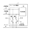
以下、本発明の参考例について図面を参照して説明する。図1は本発明の第1の参考例に係るフィールド機器の構成を示す回路図である。フィールド機器1は、各種の機能を実現する内部回路10と、ノイズ対策回路11とを備えている。
[ First reference example ]
Hereinafter, reference examples of the present invention will be described with reference to the drawings. FIG. 1 is a circuit diagram showing a configuration of a field device according to a first reference example of the present invention. The
内部回路10は、例えばバルブの開度を制御したり(フィールド機器1がバルブポジショナの場合)、2点間の圧力の差または絶対圧を測定したりする(フィールド機器1が圧力発信器の場合)ための回路である。なお、フィールド機器1は、バルブポジショナや圧力発信器に限らないことは言うまでもない。
The
ノイズ対策回路11は、図示しない電源からフィールド機器1の内部回路10へ正の電源電圧を供給する+電源線L1(第1の電源線)とアースAとの間に挿入されるコンデンサC1と、電源から内部回路10へ負の電源電圧(例えばグランド電位)を供給する−電源線L2(第2の電源線)とアースAとの間に挿入されるコンデンサC2と、+電源線L1とアースAとの間にコンデンサC1と直列に挿入されるスイッチSW1と、−電源線L2とアースAとの間にコンデンサC2と直列に挿入されるスイッチSW2とから構成される。
The
このように、本参考例では、+電源線L1とアースAとの間に、スイッチSW1とコンデンサC1とを直列に接続した第1の容量調整部12−1を挿入し、−電源線L2とアースAと間に、スイッチSW2とコンデンサC2とを直列に接続した第2の容量調整部12−2を挿入している。 As described above, in this reference example , the first capacitance adjusting unit 12-1 in which the switch SW1 and the capacitor C1 are connected in series is inserted between the + power supply line L1 and the ground A, and the-power supply line L2 and A second capacitance adjusting unit 12-2, in which the switch SW2 and the capacitor C2 are connected in series, is inserted between the ground A and the ground A.
これにより、本参考例では、フィールド機器1が設置される現場でフィールド機器1の電源線L1,L2がアースAに対して有する容量成分が適切になるようにスイッチSW1,SW2のON/OFFを設定して容量調整部12−1,12−2の容量を調整することによりノイズ経路を調整することができ、フィールド機器1や電源の改造・交換を行うことなくノイズ対策を実施することができる。
As a result, in this reference example , the switches SW1 and SW2 are turned ON / OFF so that the capacitance components of the power lines L1 and L2 of the
図2を用いて本参考例の効果を説明する。ここでは、電源2の内部で−電源線L2がアースA2に接地されている場合について説明する。従来と同様に、図2の例では、電源側アースA2とフィールド機器側アースA1との間に例えば抵抗成分に起因するノイズ源Nが存在する。
The effect of this reference example will be described with reference to FIG. Here, a case where the-power supply line L2 is grounded to the ground A2 inside the
ノイズ対策回路11のスイッチSW1をOFFに設定し、スイッチSW2をONに設定したときに、電源側アースA2を基準としてノイズ電圧の経路を考察すると、スイッチSW1をOFFに設定したことにより、フィールド機器側アースA1とコンデンサC1とを介したノイズ経路3が遮断されるので、+電源線L1にノイズ電圧が伝わることはない。一方、−電源線L2は、電源側アースA2と同じ電位となる。この状態において、フィールド機器1の+電源線L1と−電源線L2との間にはノイズ電位差が生じないため、従来のようなノイズ電流が内部回路10に流れることはない。このように、本参考例では、スイッチSW1,SW2のON/OFFを適切に設定することにより、ノイズ対策を実施することができる。
When the switch SW1 of the
図1、図2では、スイッチとコンデンサとを直列に接続した回路を1電源線あたり1個としたが、これに限るものではなく、図3に示すようにスイッチとコンデンサとを直列に接続した回路を1電源線あたり複数個設けるようにしてもよい。+電源線L1とアースAとの間に、スイッチSW1とコンデンサC1とを直列に接続した回路を並列に複数配設した回路は第1の容量調整部12−1aを構成している。また、−電源線L2とアースAと間に、スイッチSW2とコンデンサC2とを直列に接続した回路を並列に複数配設した回路は第2の容量調整部12−2aを構成している。 In FIGS. 1 and 2, the number of circuits in which the switch and the capacitor are connected in series is one per power line, but the present invention is not limited to this, and the switch and the capacitor are connected in series as shown in FIG. A plurality of circuits may be provided per power line. A circuit in which a plurality of circuits in which a switch SW1 and a capacitor C1 are connected in series are arranged in parallel between the + power line L1 and the ground A constitutes a first capacitance adjusting unit 12-1a. Further, a circuit in which a plurality of circuits in which a switch SW2 and a capacitor C2 are connected in series are arranged in parallel between the power line L2 and the ground A constitutes a second capacitance adjusting unit 12-2a.
図3に示したフィールド機器1aのノイズ対策回路11aによれば、フィールド機器1aの電源線L1,L2がアースAに対して有する容量を細かく調整することができ、より適切なノイズ対策を実施することが可能となる。
According to the
なお、スイッチSW1,SW2は機械的な操作によってON/OFFを設定できるものであってもよいし、外部からの制御信号によってON/OFFを設定できるものであってもよい。 The switches SW1 and SW2 may be set to ON / OFF by mechanical operation, or may be set to ON / OFF by a control signal from the outside.
[第2の参考例]
次に、本発明の第2の参考例について説明する。図4は本発明の第2の参考例に係るフィールド機器の構成を示す回路図であり、図1、図3と同一の構成には同一の符号を付してある。本参考例のフィールド機器1bは、内部回路10と、ノイズ対策回路11bとを備えている。
[ Second reference example ]
Next, a second reference example of the present invention will be described. FIG. 4 is a circuit diagram showing the configuration of the field device according to the second reference example of the present invention, and the same configurations as those in FIGS. 1 and 3 are designated by the same reference numerals. The
ノイズ対策回路11bは、+電源線L1とアースAとの間に挿入されるバリアブルコンデンサC3と、−電源線L2とアースAとの間に挿入されるバリアブルコンデンサC4とから構成される。バリアブルコンデンサC3は第1の容量調整部12−1bを構成し、バリアブルコンデンサC4は第2の容量調整部12−1bを構成している。
The
このように、本参考例では、スイッチとコンデンサとを直列に接続した回路の代わりにバリアブルコンデンサC3,C4を用いることにより、フィールド機器1の電源線L1,L2がアースAに対して有する容量を連続的に調整することができ、より適切なノイズ対策を実施することが可能となる。
As described above, in this reference example , by using the variable capacitors C3 and C4 instead of the circuit in which the switch and the capacitor are connected in series, the capacities of the power supply lines L1 and L2 of the
なお、バリアブルコンデンサC3,C4は、機械的な操作によって容量が変化するものであってもよいし、外部からの制御信号によって容量が変化するものであってもよい。 The variable capacitors C3 and C4 may have capacities that change by mechanical operation, or may have capacities that change by a control signal from the outside.
[第1の実施例]
次に、本発明の第1の実施例について説明する。図5は本発明の第1の実施例に係るフィールド機器の構成を示す回路図であり、図1、図3、図4と同一の構成には同一の符号を付してある。本実施例のフィールド機器1cは、内部回路10と、ノイズ対策回路11cとを備えている。第1の参考例では、フィールド機器の設置場所でノイズ対策を行う作業員がスイッチSW1,SW2のON/OFF設定を試行錯誤で決定する必要があった。これに対して、本実施例は、スイッチSW1,SW2のON/OFF設定を自動的に最適化するものである。
[ First Example ]
Next, a first embodiment of the present invention will be described. FIG. 5 is a circuit diagram showing the configuration of the field device according to the first embodiment of the present invention, and the same configurations as those in FIGS. 1, 3, and 4 are designated by the same reference numerals. The
ノイズ対策回路11cは、コンデンサC1,C2と、スイッチSW1,SW2と、+電源線L1と−電源線L2との間の交流電位差(第1の交流電位差)を測定する測定部110と、+電源線L1とアースAとの間の交流電位差(第2の交流電位差)を測定する測定部111と、−電源線L2とアースAとの間の交流電位差(第3の交流電位差)を測定する測定部112と、測定部110の測定結果と基準値との大小判定、および測定部111,112の測定結果の大小判定を行う判定部113と、判定部113の判定結果に応じてスイッチSW1,SW2のON/OFFを制御して容量を調整する制御部114とから構成される。本実施例では、スイッチSW1,SW2として、制御部114からの制御信号によってON/OFFを設定できるものを用いる。
The noise countermeasure circuit 11c includes capacitors C1 and C2, switches SW1 and SW2, a measuring
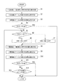
図6は本実施例のノイズ対策回路11cの動作を説明するフローチャートである。初期状態では、制御部114はスイッチSW1,SW2を共にON状態とする。測定部110は、+電源線L1と−電源線L2との間の交流電位差V12を測定する(図6ステップS1)。測定部111は、+電源線L1とアースAとの間の交流電位差V1を測定する(図6ステップS2)。測定部112は、−電源線L2とアースAとの間の交流電位差V2を測定する(図6ステップS3)。測定部110〜112は、交流電位差V12,V1,V2のピーク値を検出してもよいし、平均値を検出してもよい。
FIG. 6 is a flowchart illustrating the operation of the noise suppression circuit 11c of this embodiment. In the initial state, the
続いて、判定部113は、測定部110によって測定された交流電位差V12と予め定められた基準値Vrefとの大小判定を行う。判定部113は、|V12|<Vref、すなわち交流電位差V12の絶対値が基準値Vrefよりも小さい場合(図6ステップS4においてYES)、内部回路10がノイズの影響を受ける可能性はないと判断する。制御部114は、交流電位差V12の絶対値が基準値Vrefよりも小さい場合、現在のスイッチSW1,SW2の状態(ここでは共にONの状態)を維持して、処理を終了する。
Subsequently, the
基準値Vrefの決定は、例えば内部回路10がノイズの影響を受けない状態からノイズの影響を受ける状態に遷移する状況を現場で実験的に作り出し、この内部回路10の状態が遷移するときの交流電位差V12の絶対値を基準値Vrefとして設定すればよい。
The determination of the reference value Vref creates, for example, a situation in which the
判定部113は、交流電位差V12の絶対値が基準値Vref以上の場合(ステップS4においてYES)、内部回路10がノイズの影響を受ける可能性があると判断し、測定部111によって測定された交流電位差V1と測定部112によって測定された交流電位差V2との大小判定を行う。交流電位差V1はコンデンサC1の両端電圧に相当し、交流電位差V2はコンデンサC2の両端電圧に相当する。
The
判定部113は、|V1|<|V2|、すなわち交流電位差V1の絶対値が交流電位差V2の絶対値よりも小さい場合(図6ステップS5においてYES)、フィールド機器側アースA1とコンデンサC1とを介して+電源線L1に至る経路がノイズ経路であると判断する。つまり、交流電位差V1が小さい分だけノイズ電圧が内部回路10に印加されていることになる。制御部114は、交流電位差V1の絶対値が交流電位差V2の絶対値よりも小さい場合、スイッチSW1をONからOFFに切り替え、現在のスイッチSW2の状態(ここではON)を維持して(図6ステップS6)、処理を終了する。
When the
判定部113は、|V1|>|V2|、すなわち交流電位差V1の絶対値が交流電位差V2の絶対値よりも大きい場合(ステップS5においてNO)、フィールド機器側アースA1とコンデンサC2とを介して−電源線L2に至る経路がノイズ経路であると判断する。つまり、交流電位差V2が小さい分だけノイズ電圧が内部回路10に印加されていることになる。制御部114は、交流電位差V1の絶対値が交流電位差V2の絶対値よりも大きい場合、現在のスイッチSW1の状態(ここではON)を維持して、スイッチSW2をONからOFFに切り替え(図6ステップS7)、処理を終了する。判定部113と制御部114の動作を表1に示す。
When the absolute value of the AC potential difference V1 is larger than the absolute value of the AC potential difference V2 (NO in step S5), the

以上のように、本実施例では、フィールド機器1cが設置される現場でフィールド機器1cの電源線L1,L2がアースAに対して有する容量成分が適切になるようにスイッチSW1,SW2のON/OFFを自動的に最適化することができ、適切なノイズ対策を自動的に実施することが可能となる。
As described above, in this embodiment, the switches SW1 and SW2 are turned ON / SW2 so that the capacitance components of the power lines L1 and L2 of the
本実施例は、スイッチとコンデンサとを直列に接続した回路を1電源線あたり複数個設ける構成に適用してもよい。この場合のフィールド機器1dの構成を図7に示し、ノイズ対策回路11dの動作を図8に示す。図8のステップS1〜S4の処理は上記のとおりである。
This embodiment may be applied to a configuration in which a plurality of circuits in which a switch and a capacitor are connected in series are provided per power line. The configuration of the
ノイズ対策回路11dの判定部113dは、交流電位差V12と基準値Vrefとの大小判定を上記のとおり行い(図8ステップS4)、交流電位差V12の絶対値が基準値Vref以上の場合、交流電位差V1と交流電位差V2との大小判定に応じた処理を上記のとおり行う(図8ステップS5〜S7)。そして、判定部113dは、ステップS5〜S7の処理後に、測定部110〜112の測定結果を再び取得し(図8ステップS8〜S10)、交流電位差V12の絶対値が基準値Vrefよりも小さくなるまで(図8ステップS11においてYES)、あるいは状態を変更すべきスイッチの側にON状態からOFF状態に変更できるスイッチが存在しなくなるまで(図8ステップS12においてNO)、ステップS5〜S7の処理を繰り返し実行する。
The
例えば判定部113dは、制御部114dによって複数のスイッチSW1の中の1つがON状態からOFF状態に変更された後に(ステップS6)、最新の交流電位差V12の絶対値が未だ基準値Vref以上で(ステップS11においてNO)、複数のスイッチSW1の中にON状態のスイッチが残っている場合(ステップS12においてYES)、ステップS5に戻る。また、判定部113dは、制御部114dによって複数のスイッチSW2の中の1つがON状態からOFF状態に変更された後に(ステップS7)、最新の交流電位差V12の絶対値が未だ基準値Vref以上で(ステップS11においてNO)、複数のスイッチSW2の中にON状態のスイッチが残っている場合(ステップS12においてYES)、ステップS5に戻る。
For example, in the
こうして、交流電位差V12の絶対値が小さくなる方向に(交流電位差V1の絶対値と交流電位差V2の絶対値とが等しい値になるように)、複数のスイッチSW1,SW2のON/OFFを自動的に最適化することができ、より適切なノイズ対策を実施することが可能となる。 In this way, the plurality of switches SW1 and SW2 are automatically turned ON / OFF in the direction in which the absolute value of the AC potential difference V12 becomes smaller (so that the absolute value of the AC potential difference V1 and the absolute value of the AC potential difference V2 become equal). It can be optimized to, and more appropriate noise countermeasures can be implemented.
[第2の実施例]
次に、本発明の第2の実施例について説明する。図9は本発明の第2の実施例に係るフィールド機器の構成を示す回路図であり、図1、図3〜図5、図7と同一の構成には同一の符号を付してある。本実施例のフィールド機器1eは、内部回路10と、ノイズ対策回路11eとを備えている。第2の参考例では、フィールド機器の設置場所でノイズ対策を行う作業員がバリアブルコンデンサC3,C4の容量を試行錯誤で決定する必要があった。これに対して、本実施例は、バリアブルコンデンサC3,C4の容量を自動的に最適化するものである。
[ Second Example ]
Next, a second embodiment of the present invention will be described. FIG. 9 is a circuit diagram showing the configuration of the field device according to the second embodiment of the present invention, and the same configurations as those in FIGS. 1, 3 to 5, and 7 are designated by the same reference numerals. The field device 1e of this embodiment includes an
ノイズ対策回路11eは、バリアブルコンデンサC3,C4と、測定部110〜112と、判定部113eと、判定部113eの判定結果に応じてバリアブルコンデンサC3,C4の容量を調整する制御部114eとから構成される。本実施例では、バリアブルコンデンサC3,C4として、制御部114eからの制御信号によって容量を変更できるものを用いる。
The noise suppression circuit 11e includes variable capacitors C3 and C4,
図10は本実施例のノイズ対策回路11eの動作を説明するフローチャートである。図10のステップS1〜S5の処理は第1の実施例で説明したとおりである。
制御部114eは、交流電位差V1の絶対値が交流電位差V2の絶対値よりも小さい場合(図10ステップS5においてYES)、バリアブルコンデンサC3の容量が所定量だけ小さくなるように制御し、バリアブルコンデンサC4の現在の容量を維持する(図10ステップS13)。
FIG. 10 is a flowchart illustrating the operation of the noise suppression circuit 11e of this embodiment. The processing of steps S1 to S5 in FIG. 10 is as described in the first embodiment.
When the absolute value of the AC potential difference V1 is smaller than the absolute value of the AC potential difference V2 (YES in step S5 in FIG. 10), the
また、制御部114eは、交流電位差V1の絶対値が交流電位差V2の絶対値よりも大きい場合(ステップS5においてNO)、バリアブルコンデンサC4の容量が所定量だけ小さくなるように制御し、バリアブルコンデンサC3の現在の容量を維持する(図10ステップS14)。
Further, when the absolute value of the AC potential difference V1 is larger than the absolute value of the AC potential difference V2 (NO in step S5), the
判定部113eは、ステップS5,S13,S14の処理後に、測定部110〜112の測定結果を再び取得し(図10ステップS15〜S17)、交流電位差V12の絶対値が基準値Vrefよりも小さくなるまで(図10ステップS18においてYES)、あるいは変更すべきバリアブルコンデンサの容量が下限に達して容量を変更できなくなるまで(図10ステップS19においてNO)、ステップS5,S13,S14の処理を繰り返し実行する。
After the processing of steps S5, S13, and S14, the
例えば判定部113eは、制御部114eによってバリアブルコンデンサC3の容量が削減された後に(ステップS13)、最新の交流電位差V12の絶対値が未だ基準値Vref以上で(ステップS18においてNO)、バリアブルコンデンサC3の容量を更に削減することが可能(C3の容量を削減する方向に制御信号を変更可能)な場合(ステップS19においてYES)、ステップS5に戻る。また、判定部113eは、制御部114eによってバリアブルコンデンサC4の容量が削減された後に(ステップS14)、最新の交流電位差V12の絶対値が未だ基準値Vref以上で(ステップS18においてNO)、バリアブルコンデンサC4の容量を更に削減することが可能(C4の容量を削減する方向に制御信号を変更可能)な場合(ステップS19においてYES)、ステップS5に戻る。
For example, in the
こうして、交流電位差V12の絶対値が小さくなる方向に(交流電位差V1の絶対値と交流電位差V2の絶対値とが等しい値になるように)、バリアブルコンデンサC3,C4の容量を自動的に最適化することができ、より適切なノイズ対策を実施することが可能となる。判定部113eと制御部114eの動作を表2に示す。
In this way, the capacitances of the variable capacitors C3 and C4 are automatically optimized so that the absolute value of the AC potential difference V12 becomes smaller (so that the absolute value of the AC potential difference V1 and the absolute value of the AC potential difference V2 become equal). It is possible to take more appropriate noise countermeasures. Table 2 shows the operations of the
なお、図6、図8、図10に示した処理は、例えばフィールド機器1c,1d,1eの電源が投入されたときに1回実施してもよいし、一定時間毎に実施してもよいし、作業員から指示があったときに実施してもよい。
The processes shown in FIGS. 6, 8 and 10 may be performed once when the power of the
第1、第2の実施例で説明した判定部113,113d,113eは、例えばCPU(Central Processing Unit)、記憶装置及びインタフェースを備えたコンピュータと、これらのハードウェア資源を制御するプログラムによって実現することができる。CPUは、記憶装置に格納されたプログラムに従って第1、第2の実施例で説明した処理を実行する。
The
第1、第2の参考例および第1、第2の実施例では、ノイズ対策回路11,11a〜11eをフィールド機器1,1a〜1eの内部に設けたが、これに限るものではなく、ノイズ対策回路11,11a〜11eをフィールド機器1,1a〜1eの外部に設けるようにしてもよい。ただし、ノイズ対策回路11,11a〜11eの地点のアースとフィールド機器1,1a〜1eの地点のアースとの距離が長くなることを避けるため、ノイズ対策回路11,11a〜11eをフィールド機器1,1a〜1eの近傍に設けることが望ましい。
In the first and second reference examples and the first and second embodiments , the
第1の参考例および第1の実施例では、スイッチSW1とコンデンサC1とを直接的に接続した回路を第1の容量調整部12−1とし、スイッチSW2とコンデンサC2とを直接的に接続した回路を第2の容量調整部12−2としているが、容量調整部12−1,12−2はこのような形態に限るものではない。例えばスイッチSW1とコンデンサC1との間、およびスイッチSW2とコンデンサC2との間のそれぞれに、抵抗等の素子や回路が挿入されていてもよい。すなわち、コンデンサC1,C2は、それぞれスイッチSW1,SW2と同列状に電源線とアースとの間に挿入され、スイッチSW1,SW2と直接的または間接的に接続されていればよい。 In the first reference example and the first embodiment , the circuit in which the switch SW1 and the capacitor C1 are directly connected is used as the first capacitance adjusting unit 12-1, and the switch SW2 and the capacitor C2 are directly connected. Although the circuit is a second capacitance adjusting section 12-2, the capacitance adjusting sections 12-1 and 12-2 are not limited to such a form. For example, an element or circuit such as a resistor may be inserted between the switch SW1 and the capacitor C1 and between the switch SW2 and the capacitor C2, respectively. That is, the capacitors C1 and C2 may be inserted between the power supply line and the ground in the same row as the switches SW1 and SW2, respectively, and may be directly or indirectly connected to the switches SW1 and SW2.
図3、図7に示した第1の容量調整部12−1aにおいてもスイッチSW1とコンデンサC1とを含む回路を1電源線あたり複数個設けるようにすればよく、個々のコンデンサC1は同列のスイッチSW1と直接的または間接的に接続されていればよい。同様に、第2の容量調整部12−2aにおいてもスイッチSW2とコンデンサC2とを含む回路を1電源線あたり複数個設けるようにすればよく、個々のコンデンサC2は同列のスイッチSW2と直接的または間接的に接続されていればよい。 Also in the first capacitance adjusting unit 12-1a shown in FIGS. 3 and 7, a plurality of circuits including the switch SW1 and the capacitor C1 may be provided per power line, and the individual capacitors C1 are switches in the same row. It may be directly or indirectly connected to SW1. Similarly, in the second capacitance adjusting unit 12-2a, a plurality of circuits including the switch SW2 and the capacitor C2 may be provided per power supply line, and each capacitor C2 may be directly or directly with the switch SW2 in the same row. It suffices if it is indirectly connected.
本発明は、フィールド機器のノイズ対策に適用することができる。 The present invention can be applied to noise suppression of field equipment.
1,1a〜1e…フィールド機器、10…内部回路、11,11a〜11e…ノイズ対策回路、12−1,12−1a,12−1b,12−2,12−2a,12−1b…容量調整部、110〜112…測定部、113,113d,113e…判定部、114,114d,114e…制御部、L1,L2…電源線、A…アース、C1,C2…コンデンサ、C3,C4…バリアブルコンデンサ、SW1,SW2…スイッチ。 1,1a to 1e ... Field equipment, 10 ... Internal circuit, 11,11a to 11e ... Noise suppression circuit, 12-1, 12-1a, 12-1b, 12-2, 12-2a, 12-1b ... Capacitor adjustment Unit 110-112 ... Measurement unit, 113, 113d, 113e ... Judgment unit, 114, 114d, 114e ... Control unit, L1, L2 ... Power line, A ... Earth, C1, C2 ... Capacitor, C3, C4 ... Variable capacitor , SW1, SW2 ... Switch.
Claims (4)
前記電源から前記フィールド機器の内部回路へ第2の電源電圧を供給する第2の電源線と前記アースとの間に挿入され、容量が調整可能なように構成された第2の容量調整部と、
前記第1の電源線と前記第2の電源線との間の第1の交流電位差を測定するように構成された第1の測定部と、
前記第1の電源線と前記アースとの間の第2の交流電位差を測定するように構成された第2の測定部と、
前記第2の電源線と前記アースとの間の第3の交流電位差を測定するように構成された第3の測定部と、
前記第1の交流電位差と基準値との大小判定、および前記第2の交流電位差と前記第3の交流電位差の大小判定を行うように構成された判定部と、
前記判定部の判定結果に応じて前記第1、第2の容量調整部の容量を調整するように構成された制御部とを備えることを特徴とするノイズ対策回路。 A first capacity adjusting unit inserted between the first power line that supplies the first power supply voltage from the power supply to the internal circuit of the field equipment and the ground, and configured so that the capacity can be adjusted .
With a second capacity adjusting unit inserted between the second power supply line for supplying a second power supply voltage from the power supply to the internal circuit of the field equipment and the ground, and configured so that the capacity can be adjusted. ,
A first measuring unit configured to measure a first AC potential difference between the first power line and the second power line.
A second measuring unit configured to measure a second AC potential difference between the first power line and the ground.
A third measuring unit configured to measure a third AC potential difference between the second power line and the ground.
A determination unit configured to determine the magnitude of the first AC potential difference and the reference value, and to determine the magnitude of the second AC potential difference and the third AC potential difference.
A noise suppression circuit comprising a control unit configured to adjust the capacity of the first and second capacity adjusting units according to a determination result of the determination unit.
前記制御部は、前記第1の交流電位差が前記基準値以上の場合に、前記第2の交流電位差と前記第3の交流電位差の大小判定の結果に基づいて、前記第1の交流電位差が小さくなる方向に前記第1、第2の容量調整部の容量を調整することを特徴とするノイズ対策回路。 In the noise suppression circuit according to claim 1,
When the first AC potential difference is equal to or greater than the reference value, the control unit has a small first AC potential difference based on the result of determining the magnitude of the second AC potential difference and the third AC potential difference. A noise countermeasure circuit characterized in that the capacitance of the first and second capacitance adjusting sections is adjusted in the direction of
前記制御部は、前記第1の交流電位差が前記基準値以上の場合で、かつ前記第2の交流電位差が前記第3の交流電位差よりも小さい場合に、前記第1の容量調整部の容量が減る方向に調整し、前記第1の交流電位差が前記基準値以上の場合で、かつ前記第2の交流電位差が前記第3の交流電位差よりも大きい場合に、前記第2の容量調整部の容量が減る方向に調整することを特徴とするノイズ対策回路。 In the noise suppression circuit according to claim 2,
When the first AC potential difference is equal to or greater than the reference value and the second AC potential difference is smaller than the third AC potential difference, the control unit has the capacity of the first capacity adjusting unit. When the first AC potential difference is equal to or greater than the reference value and the second AC potential difference is larger than the third AC potential difference, the capacity of the second capacity adjusting unit is adjusted. A noise suppression circuit characterized by adjusting in the direction of decreasing voltage.
Priority Applications (1)
| Application Number | Priority Date | Filing Date | Title |
|---|---|---|---|
| JP2017105448A JP6974035B2 (en) | 2017-05-29 | 2017-05-29 | Noise suppression circuit and field equipment |
Applications Claiming Priority (1)
| Application Number | Priority Date | Filing Date | Title |
|---|---|---|---|
| JP2017105448A JP6974035B2 (en) | 2017-05-29 | 2017-05-29 | Noise suppression circuit and field equipment |
Publications (2)
| Publication Number | Publication Date |
|---|---|
| JP2018201309A JP2018201309A (en) | 2018-12-20 |
| JP6974035B2 true JP6974035B2 (en) | 2021-12-01 |
Family
ID=64667428
Family Applications (1)
| Application Number | Title | Priority Date | Filing Date |
|---|---|---|---|
| JP2017105448A Active JP6974035B2 (en) | 2017-05-29 | 2017-05-29 | Noise suppression circuit and field equipment |
Country Status (1)
| Country | Link |
|---|---|
| JP (1) | JP6974035B2 (en) |
Families Citing this family (1)
| Publication number | Priority date | Publication date | Assignee | Title |
|---|---|---|---|---|
| JP2020148502A (en) * | 2019-03-11 | 2020-09-17 | トヨタ自動車株式会社 | Current measuring device |
Family Cites Families (7)
| Publication number | Priority date | Publication date | Assignee | Title |
|---|---|---|---|---|
| JPS6176026A (en) * | 1984-09-19 | 1986-04-18 | 日本電気株式会社 | Preventive circuit for inrush current |
| JPH06113534A (en) * | 1992-09-25 | 1994-04-22 | Matsushita Electric Works Ltd | Power supply |
| JP2006018665A (en) * | 2004-07-02 | 2006-01-19 | Matsushita Electric Ind Co Ltd | Power supply stabilization control device |
| JP5493902B2 (en) * | 2009-10-28 | 2014-05-14 | 富士電機株式会社 | Power converter |
| JP6131742B2 (en) * | 2012-09-28 | 2017-05-24 | 株式会社デンソー | Electronic equipment |
| JP2017020631A (en) * | 2015-07-15 | 2017-01-26 | アズビル株式会社 | Positioner |
| JP2017041920A (en) * | 2015-08-17 | 2017-02-23 | 東芝シュネデール・インバータ株式会社 | Inverter device |
-
2017
- 2017-05-29 JP JP2017105448A patent/JP6974035B2/en active Active
Also Published As
| Publication number | Publication date |
|---|---|
| JP2018201309A (en) | 2018-12-20 |
Similar Documents
| Publication | Publication Date | Title |
|---|---|---|
| TWI636352B (en) | Voltage regulator | |
| US10613566B2 (en) | Real-time slope control apparatus for voltage regulator and operating method thereof | |
| US10970154B2 (en) | Method for detecting a failure in an electronic system | |
| JP6974035B2 (en) | Noise suppression circuit and field equipment | |
| TWI643050B (en) | Voltage regulator | |
| JP6513943B2 (en) | Voltage regulator | |
| EP1929391B1 (en) | An integrated circuit and a method for selecting a voltage in an integrated circuit | |
| TW201504784A (en) | Voltage regulator | |
| CN112889015B (en) | Method and apparatus to improve the safe operating area of a switched mode power supply | |
| US10956646B2 (en) | Customizing circuit layout design rules for fabrication facilities | |
| US20170093226A1 (en) | Methods and circuits for monitoring and regulating voltage across a low voltage device driven by a long line carrying radio frequency signals | |
| CN104810783B (en) | Analog current output module | |
| JP6592978B2 (en) | Input pre-circuit in switching power supply control IC and switching power supply control apparatus having the input pre-circuit | |
| KR101810504B1 (en) | Integrated analog signal processing apparatus and method thereof | |
| JP6908366B2 (en) | Power circuit and power control method | |
| KR101997360B1 (en) | Apparatus for detecting disconnection of inductive sensor | |
| KR101796769B1 (en) | Capacitorless low drop out regulator and controlling circuit therefor | |
| JP2020092331A (en) | Power supply controller | |
| JP2007304850A (en) | Voltage generation circuit and electric appliance provided with the same | |
| KR20150059300A (en) | Apparatus and method for voltage distribution | |
| EP3118582A1 (en) | Feedback control device | |
| KR101525701B1 (en) | Apparatus for controlling output voltage and apparatus for boosting voltage including the same | |
| TW201929365A (en) | Power supply system and control method for power supply system | |
| KR102049398B1 (en) | Linear Mode DC Power Supply Device | |
| JP5744712B2 (en) | Power detection circuit |
Legal Events
| Date | Code | Title | Description |
|---|---|---|---|
| A621 | Written request for application examination |
Free format text: JAPANESE INTERMEDIATE CODE: A621 Effective date: 20200311 |
|
| A977 | Report on retrieval |
Free format text: JAPANESE INTERMEDIATE CODE: A971007 Effective date: 20210129 |
|
| A131 | Notification of reasons for refusal |
Free format text: JAPANESE INTERMEDIATE CODE: A131 Effective date: 20210224 |
|
| A521 | Written amendment |
Free format text: JAPANESE INTERMEDIATE CODE: A523 Effective date: 20210423 |
|
| TRDD | Decision of grant or rejection written | ||
| A01 | Written decision to grant a patent or to grant a registration (utility model) |
Free format text: JAPANESE INTERMEDIATE CODE: A01 Effective date: 20211012 |
|
| A61 | First payment of annual fees (during grant procedure) |
Free format text: JAPANESE INTERMEDIATE CODE: A61 Effective date: 20211104 |
|
| R150 | Certificate of patent or registration of utility model |
Ref document number: 6974035 Country of ref document: JP Free format text: JAPANESE INTERMEDIATE CODE: R150 |