EP2882083B1 - Bridgeless power factor correction circuit - Google Patents
Bridgeless power factor correction circuit Download PDFInfo
- Publication number
- EP2882083B1 EP2882083B1 EP13195824.1A EP13195824A EP2882083B1 EP 2882083 B1 EP2882083 B1 EP 2882083B1 EP 13195824 A EP13195824 A EP 13195824A EP 2882083 B1 EP2882083 B1 EP 2882083B1
- Authority
- EP
- European Patent Office
- Prior art keywords
- switch
- capacitor
- controllable
- input
- output terminal
- Prior art date
- Legal status (The legal status is an assumption and is not a legal conclusion. Google has not performed a legal analysis and makes no representation as to the accuracy of the status listed.)
- Not-in-force
Links
Images


Classifications
-
- H—ELECTRICITY
- H02—GENERATION; CONVERSION OR DISTRIBUTION OF ELECTRIC POWER
- H02M—APPARATUS FOR CONVERSION BETWEEN AC AND AC, BETWEEN AC AND DC, OR BETWEEN DC AND DC, AND FOR USE WITH MAINS OR SIMILAR POWER SUPPLY SYSTEMS; CONVERSION OF DC OR AC INPUT POWER INTO SURGE OUTPUT POWER; CONTROL OR REGULATION THEREOF
- H02M1/00—Details of apparatus for conversion
- H02M1/0083—Converters characterised by their input or output configuration
- H02M1/0085—Partially controlled bridges
-
- H—ELECTRICITY
- H02—GENERATION; CONVERSION OR DISTRIBUTION OF ELECTRIC POWER
- H02M—APPARATUS FOR CONVERSION BETWEEN AC AND AC, BETWEEN AC AND DC, OR BETWEEN DC AND DC, AND FOR USE WITH MAINS OR SIMILAR POWER SUPPLY SYSTEMS; CONVERSION OF DC OR AC INPUT POWER INTO SURGE OUTPUT POWER; CONTROL OR REGULATION THEREOF
- H02M1/00—Details of apparatus for conversion
- H02M1/42—Circuits or arrangements for compensating for or adjusting power factor in converters or inverters
- H02M1/4208—Arrangements for improving power factor of AC input
- H02M1/4225—Arrangements for improving power factor of AC input using a non-isolated boost converter
-
- H—ELECTRICITY
- H02—GENERATION; CONVERSION OR DISTRIBUTION OF ELECTRIC POWER
- H02J—CIRCUIT ARRANGEMENTS OR SYSTEMS FOR SUPPLYING OR DISTRIBUTING ELECTRIC POWER; SYSTEMS FOR STORING ELECTRIC ENERGY
- H02J3/00—Circuit arrangements for ac mains or ac distribution networks
- H02J3/01—Arrangements for reducing harmonics or ripples
-
- H—ELECTRICITY
- H02—GENERATION; CONVERSION OR DISTRIBUTION OF ELECTRIC POWER
- H02M—APPARATUS FOR CONVERSION BETWEEN AC AND AC, BETWEEN AC AND DC, OR BETWEEN DC AND DC, AND FOR USE WITH MAINS OR SIMILAR POWER SUPPLY SYSTEMS; CONVERSION OF DC OR AC INPUT POWER INTO SURGE OUTPUT POWER; CONTROL OR REGULATION THEREOF
- H02M1/00—Details of apparatus for conversion
- H02M1/12—Arrangements for reducing harmonics from ac input or output
- H02M1/123—Suppression of common mode voltage or current
-
- Y—GENERAL TAGGING OF NEW TECHNOLOGICAL DEVELOPMENTS; GENERAL TAGGING OF CROSS-SECTIONAL TECHNOLOGIES SPANNING OVER SEVERAL SECTIONS OF THE IPC; TECHNICAL SUBJECTS COVERED BY FORMER USPC CROSS-REFERENCE ART COLLECTIONS [XRACs] AND DIGESTS
- Y02—TECHNOLOGIES OR APPLICATIONS FOR MITIGATION OR ADAPTATION AGAINST CLIMATE CHANGE
- Y02B—CLIMATE CHANGE MITIGATION TECHNOLOGIES RELATED TO BUILDINGS, e.g. HOUSING, HOUSE APPLIANCES OR RELATED END-USER APPLICATIONS
- Y02B70/00—Technologies for an efficient end-user side electric power management and consumption
- Y02B70/10—Technologies improving the efficiency by using switched-mode power supplies [SMPS], i.e. efficient power electronics conversion e.g. power factor correction or reduction of losses in power supplies or efficient standby modes
-
- Y—GENERAL TAGGING OF NEW TECHNOLOGICAL DEVELOPMENTS; GENERAL TAGGING OF CROSS-SECTIONAL TECHNOLOGIES SPANNING OVER SEVERAL SECTIONS OF THE IPC; TECHNICAL SUBJECTS COVERED BY FORMER USPC CROSS-REFERENCE ART COLLECTIONS [XRACs] AND DIGESTS
- Y02—TECHNOLOGIES OR APPLICATIONS FOR MITIGATION OR ADAPTATION AGAINST CLIMATE CHANGE
- Y02E—REDUCTION OF GREENHOUSE GAS [GHG] EMISSIONS, RELATED TO ENERGY GENERATION, TRANSMISSION OR DISTRIBUTION
- Y02E40/00—Technologies for an efficient electrical power generation, transmission or distribution
- Y02E40/40—Arrangements for reducing harmonics
Definitions
- the present invention relates to a bridgeless power factor correction (PFC) circuit, and particularly to a PFC circuit for transforming a single-phase alternating current (AC) voltage to a direct current (DC) voltage.
- PFC power factor correction
- a power factor corrector or a power factor correction circuit is a front-end power stage of a grid-connected power converter, such as a power supply, motor drive and electronic ballast [1] to [3]. It is used to meet international grid current standards, such as IEEE519 and IEC-61000-3-12. These standards are also applied to a single-phase grid network which is typically used as an AC power source for low power industrial applications and household devices. Using a PFC in a system ensures a sinusoidal input current and a stable output DC voltage. It can also be foreseen that the PFC will be a very important device to ensure a good power quality in a more complex grid network.
- a diode bridge and a boost converter are used.
- the diode bridge rectifies the grid current and voltage.
- the boost converter shapes inductor current into rectified sinusoidal current.
- grid current is sinusoidal and in-phase of grid voltage.
- This converter is simple and low-cost, since only one active switch is in the circuit. Thus, it is popularly adopted by lighting applications.
- the drawback of the circuit is a high conduction loss for high power applications since there are three semiconductors in the current path, irrespective of whether the controlled switch is on or off.
- a large high frequency filter is required due to a large peak-to-peak high frequency ripple current carrying on the gird current.
- a bridgeless PFC is proposed in [4].
- the PFC integrates a diode bridge and a boost converter into one power stage, including two switching arms.
- One switching arm shapes half line cycle grid current.
- Two grid inductors are always in series, irrespective of the switching state.
- the circuit gives a low conductional loss, since it has only two semiconductors in the current paths.
- it is more expensive because of the more active device and magnetic components.
- a bridgeless PFC with a series semiconductor switch is presented in [5].
- the series switch is synchronized with a main switching for current shaping.
- grid terminals are electrically isolated during inductor current charging states.
- a low leakage current can be generated.
- it requires one higher-rated voltage, higher-rated current and higher switching frequency semiconductor switch in the main current flowing path.
- the conduction loss is higher than the simple bridgeless PFC during inductor current discharging states.
- the fundamental idea of the bridgeless PFC is distorted and it is expensive. Besides, a high frequency filter is still required.
- Another method of eliminating the common mode voltage issue is to use a bi-directional switch to charge up an input inductor current [6]. When the bi-directional switch is closed, all diodes are off due to a reverse bias by the output dc voltage. This leads to electrical isolation during that switching stage.
- a diode clamped bridgeless PFC is proposed in [7]. It provides a simple and efficient solution for tackling the common mode voltage issue.
- this bridgeless PFC two diodes connect the circuit ground to a positive terminal and a negative terminal of the AC power source, respectively. These two line frequency diodes guarantee that no common mode voltage difference occurs between the ground and the AC source.
- grid inductors work in half line cycle only, which means that two separate and identical inductors are used. The high cost and large size of the inductors are problematic. Besides, a high frequency filter is still required.
- capacitors can be used to maintain the voltage difference between the ground and the AC power sources.
- a capacitor clamped bridgeless PFC is disclosed in [9]. The capacitors are coupled to the grid terminals and the ground, whereby a low leakage current can be ensured, but a high frequency current ripple can still be found at the grid current; thus, a high frequency filter is still required.
- a built-in common filter is disclosed in [10].
- a common mode filter connects serially with boost chokes, two capacitors perform functions of voltage clamping and filtering.
- the topology effectively reduces leakage current, but it does not help in filtering out the high frequency components from the grid current.
- An object of the present invention is to provide a circuit so as to solve the above problem.
- the objects of the invention are achieved by a circuit which is characterized by what is stated in the independent claim.
- Preferred embodiments of the invention are disclosed in the dependent claims.
- the invention is based on the idea of using one or more capacitors and low frequency semiconductor switches in a bridgeless PFC circuit to formulate two different LCL filter structures for different conditions.
- the semiconductor switches connect one or more capacitors to the circuit in an alternating manner, depending on the polarity of the input AC voltage.
- the circuit of the invention does not include large inductors since a third order filter is formed by using a switching circuit at the input of the circuit.
- the high frequency components are filtered out by the LCL filter and the filter structure is changed, depending on the polarity of grid voltage. Because the LCL filter attenuates high frequency components effectively, no separate EMI filter may be required.
- the circuit of the invention provides a low leakage current since the common mode voltage is clamped by the capacitors. Further, conduction losses are low because no active or passive elements are added to the main current path. Further, the input inductance being smaller, the number of turns in the inductors is also smaller. The use of low inductance inductors increases the efficiency.
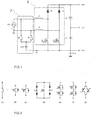
- FIG. 1 shows an embodiment of the invention.
- the PFC of the invention consists of a conventional bridgeless PFC 1 and an additional switching circuit 2.
- the switching circuit can formulate two different LCL structures, depending on grid voltage polarity.
- the conventional bridgeless PFC 1 comprises first and second input inductors L1, L2, first ends of the inductors forming first and second input terminals of the circuit. Further, the bridgeless PFC 1 comprises a series connection of a first diode D1 and a first controllable semiconductor switch S1, and a series connection of a second diode D2 and a second controllable semiconductor switch S2.
- the series connections are connected in parallel between positive and negative output terminals VDC+, VDC- of the power factor correction circuit.
- the output terminals form the output voltage of the circuit and, typically, a capacitor or a series connection of capacitors C1, C2 is connected between the output terminals.
- a middle voltage potential VM is also available.
- the second end of a first inductor L1 is connected at a point between the series connection of the first diode and the first controllable semiconductor switch, and similarly the second end of a second inductor L2 is connected at a point between the series connection of the second diode and the second controllable semiconductor switch.
- Polarities of the first and second diode D1, D2 are such that current can pass through the diode to the positive output terminal. This means that cathodes of the diodes are connected to the positive output terminal VDC+.
- the controllable semiconductor switches S1, S2 are connected such that the switches can block current from flowing through the switches to the negative output terminal.
- the bridgeless PFC circuit boosts the AC grid voltage to a higher DC bus voltage and controls the flow of DC power onto the DC bus.
- the grid current is controlled sinusoidal and in-phase to the AC grid voltage.
- a switching circuit 2 filters out switching frequency components which are generated by the bridgeless PFC.
- the switching circuit of the invention is adapted to connect a capacitor CAB; CA, CB between an input terminal and an output terminal of the power factor correction circuit in such a manner that the capacitor is connected between the first input terminal and a potential of an output terminal when input voltage connectable to the input terminals is positive.
- the capacitor is connected between the second input terminal and a potential of an output terminal when the input voltage connectable to the input terminals is negative.
- the switching circuit comprises two bi-directional switches SA, SB.
- the bi-directional switches are connected in series and one end of the series connection is connected to the first input terminal and the other end is connected to the second input terminal.
- the bridgeless PFC is shown to be connected to the input voltage VAC, whereby the first terminal is connected to Line L and the second terminal is connected to the neutral of the grid.
- the switching circuit shown in Figure 1 comprises also a capacitor CAB that is coupled between the junction point of two bi-directional switches SA, SB and any potential of the output terminals, i.e. any point of the output DC bus.
- one terminal of the capacitor Vx is shown coupled to the negative output terminal, i.e. the potential of a negative DC bus.
- the capacitor is used to clamp the potential difference between the AC power source and the ground.
- the connection is shown in dashed line to highlight the fact that the connection can also be to any other point of the DC bus, including a positive DC bus, i.e. the positive output terminal, or the middle point of the output voltage VM.
- the switch SA is conducting and the switch SB is blocking.
- the switch SB is conducting and the switch SA is blocking.
- the capacitor is connected to the input having the positive voltage.
- the capacitor is connected to the input having the negative voltage.
- the bi-directional switches SA, SB can be realized by a single-directional blocking semiconductor switch or by connecting two MOSFETs back-to-back in series or other circuits and devices which can provide bi-directional blocking and conducting characteristics.
- a body diode of a MOSFET or an anti-parallel diode of an IGBT may create a leakage path when the semiconductor switches are turned off.
- Figure 2 shows possible arrangements for the bi-directional switch SA, SB.
- Figure 2 shows an ideal switch, (b) shows a MOSFET, (c) shows an IGBT with an anti-parallel diode, (d) shows a diode bridge with a controllable switch, (e) shows a common emitter back-to-back implementation, (f) shows a common drain back-to-back implementation, and (g) shows a bi-directional switch formed of anti-parallel reverse blocking IGBTs.
- Figure 3 shows the switching states of the circuit of Figure 1 during a positive half line cycle.
- the filter capacitor CAB is connected to Line L of the grid voltage through the bi-directional switch SA.
- the main switch S2 is always conducting and the main switch S1 is switching at a high frequency.
- the switch S1 is conducting, the inductor L1 is charged, and when S1 is blocking, the inductor is boosting the output voltage.
- Figures 3(a) and 3(b) show the circuit when the main switch S1 is switching on and off, respectively.
- Figures 4(a) and 4(b) show corresponding equivalent circuits of Figures 3(a) and 3(b) , respectively.
- L1, CAB, and L2 form an LCL filter between the grid and the boost converter.
- L2 takes the role of a grid inductor, and thereby a low grid deferential current ripple is achieved.
- the capacitor CAB is coupled between Line L and the negative terminal of the DC bus, and thereby the potential difference between them is clamped, and thus a low leakage current is achieved.
- the filter capacitor CAB is connected to Neutral N of the grid voltage through the bi-directional switch SB, the main switch S1 is always conducting and the main switch S2 is switching at a high frequency.
- Figures 5(a) and 5(b) show the circuit when the main switch S2 is switching on and off, respectively.
- Figures 6(a) and 6(b) are corresponding equivalent circuits of Figures 5(a) and 5(b) , respectively.
- L2, CAB, and L1 form an LCL filter between the grid and the boost converter.
- L1 takes the role of a grid inductor, and a low grid deferential current ripple is achieved.
- the capacitor CAB is coupled between Neutral N and the negative terminal of the DC bus and the potential difference between them is clamped; therefore, a low leakage current is achieved.
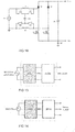
- FIG. 7 shows an embodiment of the invention.
- separate switches SA, SB connect separate capacitors CA, CB to perform the functionality described above.
- the switching circuit comprises two series connections of a switch and a capacitor.
- a first series connection SA, CA is connected between the first input terminal and a potential of an output terminal.
- a second series connection SB, CB is connected between the second input terminal and a potential of an output terminal.
- the other ends of the series connections are shown to be connected to negative output terminal.
- SA switches are on in the period of the positive half line cycle
- SB switches are on in the period of the negative half line cycle.
- the purpose of the switches is to reconfigure the LCL filter, depending on the polarity of the input voltage.
- the advantage of the topology of Figure 7 is that all semiconductor switches SA, SB, S1, and S2 are referenced to the ground, making it an attractive choice with respect to the design of gate drivers.
- FIG. 8 Another embodiment of the invention is shown in Figure 8 .
- the switching circuit in Figure 8 is coupled in X shape between the arms consisting of a series connection of a diode and a controllable switch and the AC source.
- Two bi-directional switches and two capacitors are used in the circuit. More specifically, the first series connection of a switch SA and a capacitor CA is connected in series between the first end of the first inductor and the second end of the second inductor.
- the second series connection of a switch SB and a capacitor CB is connected between the second end of the first inductor and the first end of the second inductor.
- the additional switching circuit is coupled in H shape between the arms and the AC source. Only one capacitor is used in the circuit.
- the switching circuit of the embodiment comprises two series connections of controllable switches. The first of the series connections SA1, SB2 is connected between the first terminals of the inductors L1, L2, and the second of the series connections SB1, SA2 is connected between the second ends of the inductors.
- the capacitor CAB is connected between the middle points of the series connections. In the embodiment of Figure 9 , the capacitor CAB is connected to the circuit by using the switches SA1 and SA2 during a positive half cycle and the switches SB1 and SB2 during a negative half cycle.
- the capacitor is connected between the input terminal of the circuit and the potential of the output terminal through the main switches of the circuit.
- the switch SA is conducting and the capacitor CA is connected between the first input terminal and the negative output terminal through the switch S2 which is conducting during the positive half wave.
- the capacitor CB is connected to the negative output terminal through the switch S1.
- Figure 10 shows another embodiment of the invention, in which the switching circuit is formed of four switches and one capacitor.
- the switches are arranged such that two series connections are formed and both of the series connections are connected over the the inductances L1, L2 of the input.
- the capacitor CAB is connected between the middle points of the series connections of the switches.
- the switches SA1, SA2 are controlled conductive during the positive half cycle of the input voltage, thereby connecting the capacitor between the first end of the first inductor and the second end of the second inductor.
- the second end of the second inductor is connected to the potential of the negative output terminal through the conducting switch S2.
- the switches SB1 and SB2 are controlled conductive, thereby connecting the capacitor CAB between the first end of the second inductor and the second end of the first inductor.
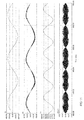
- the simulated system corresponds to that of Figure 1 .
- the input source consists of a single-phase AC voltage source, and the output is a resistor.
- the simulated output power of the PFC is 2.2 kW, the output DC voltage is 380 V, the line frequency is 50 Hz, and the input AC voltage is 230 Vrms.
- the switching frequency is 20 kHz. All semiconductors and inductors are ideal components.
- Figure 11 shows the key simulated waveforms. It can be seen that the grid current (lin, second plot) is shaped sinusoidal and in-phase to the grid voltage (first plot). Also, the current ripple is very small. The leakage current (l(Ccm), fourth plot) is small as well. The third plot shows the output voltage.
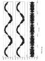
- Figure 12 shows a comparison of current waveforms using different clamping techniques in a bridgeless PFC.
- the first row of waveforms is a grid current
- the second row of waveforms is an inductor current
- the bottom row of waveforms is a leakage current.
- the inductance and switching frequency are the same in this comparison.
- Figure 12(a) shows waveforms of a conventional bridgeless PFC which is presented in [4].
- the grid current (lin) carries a large high frequency current ripple, and the leakage current is high as well (approximately 5A).
- Figure 12(b) shows diode clamped bridgeless PFC currents, the corresponding topology being presented in [7].
- the leakage current is minimized, almost to 0A, but the grid current ripple is higher than in the conventional one, since only one inductor is in the current path.
- Figure 12(c) shows capacitor clamped bridgeless PFC currents, the corresponding topology being presented in [9].
- the leakage current is minimized to an acceptable range, 0.2A_peak, but the grid current ripple is still as high as in the conventional one.
- Figure 12(d) shows capacitor clamped plus a common mode filter bridgeless PFC currents, the corresponding topology being presented in [10].
- the leakage current is further minimized, to 0.02A_peak, but to no avail as far as the grid current ripple is concerned.
- Figure 12(e) shows waveforms of the bridgeless PFC of the present invention, the corresponding topology being presented in Figure 1 .
- the leakage current is slightly higher than in the prior art solutions but still in an acceptable range, (approximately 0.4A_peak); moreover, a high quality grid current is obtained. It can be seen that the PFC of the present invention is superior to the prior art solutions in terms of high quality grid current and low leakage current.
- the present invention is usable in connection with an apparatus for sourcing AC power from an AC power grid to a DC load, such as a motor drive.
- Figure 13 and Figure 14 depict conceptual block diagrams of an exemplary two-stage power converter used to convert AC power from a single-phase grid into DC power suitable for driving an electrical load.
- the first stage of a power converter can include a Power Factor Corrector (PFC), such as a bridgeless PFC, that outputs DC power onto a DC bus.
- PFC Power Factor Corrector
- the second stage of the power converter can be an inverter ( Figure 14 ) or a DC-to-DC converter ( Figure 13 ) that supplies the power to a load.
- the voltage levels indicated in Figures 13 and 14 are examples of a commonly employed voltage.
Description
- The present invention relates to a bridgeless power factor correction (PFC) circuit, and particularly to a PFC circuit for transforming a single-phase alternating current (AC) voltage to a direct current (DC) voltage.
- A power factor corrector or a power factor correction circuit (PFC) is a front-end power stage of a grid-connected power converter, such as a power supply, motor drive and electronic ballast [1] to [3]. It is used to meet international grid current standards, such as IEEE519 and IEC-61000-3-12. These standards are also applied to a single-phase grid network which is typically used as an AC power source for low power industrial applications and household devices. Using a PFC in a system ensures a sinusoidal input current and a stable output DC voltage. It can also be foreseen that the PFC will be a very important device to ensure a good power quality in a more complex grid network.
- In a conventional PFC, a diode bridge and a boost converter are used. The diode bridge rectifies the grid current and voltage. The boost converter shapes inductor current into rectified sinusoidal current. As a result, grid current is sinusoidal and in-phase of grid voltage. This converter is simple and low-cost, since only one active switch is in the circuit. Thus, it is popularly adopted by lighting applications. However, the drawback of the circuit is a high conduction loss for high power applications since there are three semiconductors in the current path, irrespective of whether the controlled switch is on or off. Moreover, a large high frequency filter is required due to a large peak-to-peak high frequency ripple current carrying on the gird current.
- In order to solve the conduction loss issue of the conventional PFC, a bridgeless PFC is proposed in [4]. The PFC integrates a diode bridge and a boost converter into one power stage, including two switching arms. One switching arm shapes half line cycle grid current. Two grid inductors are always in series, irrespective of the switching state. The circuit gives a low conductional loss, since it has only two semiconductors in the current paths. However, it is more expensive because of the more active device and magnetic components. More importantly, there is a grounding problem, or said common mode voltage or leakage current issue, when it is operating. Besides, a high frequency filter is still required.
- Some modifications of bridgeless PFC circuits have been proposed to tackle the issue of leakage current. A bridgeless PFC with a series semiconductor switch is presented in [5]. The series switch is synchronized with a main switching for current shaping. Thus, grid terminals are electrically isolated during inductor current charging states. Then, a low leakage current can be generated. However, it requires one higher-rated voltage, higher-rated current and higher switching frequency semiconductor switch in the main current flowing path. As a result, the conduction loss is higher than the simple bridgeless PFC during inductor current discharging states. The fundamental idea of the bridgeless PFC is distorted and it is expensive. Besides, a high frequency filter is still required.
- Another method of eliminating the common mode voltage issue is to use a bi-directional switch to charge up an input inductor current [6]. When the bi-directional switch is closed, all diodes are off due to a reverse bias by the output dc voltage. This leads to electrical isolation during that switching stage.
- There are thus always two semiconductors in the current paths. However, as the diode bridge is switching at a high frequency, four expensive fast diodes have to be used. Normally, the conduction performance of a fast diode is not as good as that of line frequency diodes. A floating gate drive is another cost issue for this topology. Besides, a high frequency filter is still required.
- A diode clamped bridgeless PFC is proposed in [7]. It provides a simple and efficient solution for tackling the common mode voltage issue. In this bridgeless PFC, two diodes connect the circuit ground to a positive terminal and a negative terminal of the AC power source, respectively. These two line frequency diodes guarantee that no common mode voltage difference occurs between the ground and the AC source. However, grid inductors work in half line cycle only, which means that two separate and identical inductors are used. The high cost and large size of the inductors are problematic. Besides, a high frequency filter is still required.
- In order to solve the problem of expensive magnetic devices, a single core inductor is introduced in [8]. By means of this method, the size issue can be solved due to the use of one magnetic core. However, the design of the inductor is very difficult. Besides, a high frequency filter is still required.
- Instead of diodes, capacitors can be used to maintain the voltage difference between the ground and the AC power sources. A capacitor clamped bridgeless PFC is disclosed in [9]. The capacitors are coupled to the grid terminals and the ground, whereby a low leakage current can be ensured, but a high frequency current ripple can still be found at the grid current; thus, a high frequency filter is still required.
- A built-in common filter is disclosed in [10]. In this modification, a common mode filter connects serially with boost chokes, two capacitors perform functions of voltage clamping and filtering. The topology effectively reduces leakage current, but it does not help in filtering out the high frequency components from the grid current.
- An improved capacitor clamped approach is proposed in [11]. In this design, two switches are used to connect the voltage clamped capacitors. According to the disclosure, the additional switches are switching at the same time and the switches are used to improve the efficiency during light load operation. Thus, it can be estimated that the performance should be more or less the same as that of a simple capacitor clamped bridgeless PFC.
- Documents
US2011/096577 A1 ,CN101931319 A ,US2013/049709 A1 and Pengju Kong et al: "Common mode EMI noise suppression in bridgeless boost PFC converter", Applied power electronics conference, APEC 2007 - Twenty second annual IEEE, 1 February 2007, pages 929-935 disclose various bridgeless PFC converters. - The prior art solutions effectively solve the common mode voltage problem of the bridgeless PFC, but the penalties include a higher conduction loss and more or larger passive devices. Moreover, not all solutions can improve the grid current quality.
- An object of the present invention is to provide a circuit so as to solve the above problem. The objects of the invention are achieved by a circuit which is characterized by what is stated in the independent claim. Preferred embodiments of the invention are disclosed in the dependent claims.
- The invention is based on the idea of using one or more capacitors and low frequency semiconductor switches in a bridgeless PFC circuit to formulate two different LCL filter structures for different conditions. The semiconductor switches connect one or more capacitors to the circuit in an alternating manner, depending on the polarity of the input AC voltage.
- This reduces a grid differential mode current ripple or inductance. Further, the PFC common mode voltage is significantly reduced, since the capacitor in the LCL filter clamps the voltage between the grid and the ground.
- The circuit of the invention does not include large inductors since a third order filter is formed by using a switching circuit at the input of the circuit. The high frequency components are filtered out by the LCL filter and the filter structure is changed, depending on the polarity of grid voltage. Because the LCL filter attenuates high frequency components effectively, no separate EMI filter may be required.
- The circuit of the invention provides a low leakage current since the common mode voltage is clamped by the capacitors. Further, conduction losses are low because no active or passive elements are added to the main current path. Further, the input inductance being smaller, the number of turns in the inductors is also smaller. The use of low inductance inductors increases the efficiency.
- In the following, the invention will be described in greater detail by means of the preferred embodiments and with reference to the attached drawings, in which
-
Figure 1 shows an embodiment of the present invention; -
Figure 2 shows implementations of bi-directional switches; -
Figures 3 (a) and 3 (b) show switching states of an embodiment of the present invention during positive input voltage, -
Figures 4 (a) and 4 (b) show equivalent circuits ofFigures 3 (a) and 3 (b) ; -
Figures 5 (a) and 5 (b) show switching states of an embodiment of the present invention during negative input voltage, -
Figures 6 (a) and 6 (b) show equivalent circuits ofFigures 5 (a) and 5 (b) ; -
Figures 7 ,8 ,9 , and10 show embodiments of the invention, -
Figure 11 shows simulated waveforms of the present invention, -
Figures 12 (a) ,(b) ,(c) ,(d) ,(e) show simulated waveforms of prior art devices as compared to the present invention, -
Figures 13 and 14 show basic block diagrams depicting examples of use of the present invention. -
Figure 1 shows an embodiment of the invention. The PFC of the invention consists of a conventionalbridgeless PFC 1 and anadditional switching circuit 2. The switching circuit can formulate two different LCL structures, depending on grid voltage polarity. - The conventional
bridgeless PFC 1 comprises first and second input inductors L1, L2, first ends of the inductors forming first and second input terminals of the circuit. Further, thebridgeless PFC 1 comprises a series connection of a first diode D1 and a first controllable semiconductor switch S1, and a series connection of a second diode D2 and a second controllable semiconductor switch S2. The series connections are connected in parallel between positive and negative output terminals VDC+, VDC- of the power factor correction circuit. The output terminals form the output voltage of the circuit and, typically, a capacitor or a series connection of capacitors C1, C2 is connected between the output terminals. As a series connection of capacitors is connected between the output terminals, a middle voltage potential VM is also available. - In the circuit of the embodiment, the second end of a first inductor L1 is connected at a point between the series connection of the first diode and the first controllable semiconductor switch, and similarly the second end of a second inductor L2 is connected at a point between the series connection of the second diode and the second controllable semiconductor switch.
- Polarities of the first and second diode D1, D2 are such that current can pass through the diode to the positive output terminal. This means that cathodes of the diodes are connected to the positive output terminal VDC+. The controllable semiconductor switches S1, S2 are connected such that the switches can block current from flowing through the switches to the negative output terminal.
- The bridgeless PFC circuit boosts the AC grid voltage to a higher DC bus voltage and controls the flow of DC power onto the DC bus. The grid current is controlled sinusoidal and in-phase to the AC grid voltage.
- A switching
circuit 2 filters out switching frequency components which are generated by the bridgeless PFC. The switching circuit of the invention is adapted to connect a capacitor CAB; CA, CB between an input terminal and an output terminal of the power factor correction circuit in such a manner that the capacitor is connected between the first input terminal and a potential of an output terminal when input voltage connectable to the input terminals is positive. The capacitor is connected between the second input terminal and a potential of an output terminal when the input voltage connectable to the input terminals is negative. - Specifically, in the embodiment of
Figure 1 , the switching circuit comprises two bi-directional switches SA, SB. The bi-directional switches are connected in series and one end of the series connection is connected to the first input terminal and the other end is connected to the second input terminal. InFigure 1 , the bridgeless PFC is shown to be connected to the input voltage VAC, whereby the first terminal is connected to Line L and the second terminal is connected to the neutral of the grid. - The switching circuit shown in
Figure 1 comprises also a capacitor CAB that is coupled between the junction point of two bi-directional switches SA, SB and any potential of the output terminals, i.e. any point of the output DC bus. InFigure 1 , one terminal of the capacitor Vx is shown coupled to the negative output terminal, i.e. the potential of a negative DC bus. The capacitor is used to clamp the potential difference between the AC power source and the ground. The connection is shown in dashed line to highlight the fact that the connection can also be to any other point of the DC bus, including a positive DC bus, i.e. the positive output terminal, or the middle point of the output voltage VM. - According to the invention, during a positive half wave of the input voltage, the switch SA is conducting and the switch SB is blocking. During a negative half wave the switch SB is conducting and the switch SA is blocking. Thus, during the positive half wave of the input voltage, the capacitor is connected to the input having the positive voltage. Similarly, during the negative half wave of the input voltage, the capacitor is connected to the input having the negative voltage.
- The bi-directional switches SA, SB can be realized by a single-directional blocking semiconductor switch or by connecting two MOSFETs back-to-back in series or other circuits and devices which can provide bi-directional blocking and conducting characteristics. In practice, a body diode of a MOSFET or an anti-parallel diode of an IGBT may create a leakage path when the semiconductor switches are turned off.
Figure 2 shows possible arrangements for the bi-directional switch SA, SB. Specifically,Figure 2 (a) shows an ideal switch, (b) shows a MOSFET, (c) shows an IGBT with an anti-parallel diode, (d) shows a diode bridge with a controllable switch, (e) shows a common emitter back-to-back implementation, (f) shows a common drain back-to-back implementation, and (g) shows a bi-directional switch formed of anti-parallel reverse blocking IGBTs. -
Figure 3 shows the switching states of the circuit ofFigure 1 during a positive half line cycle. In this half line cycle, the filter capacitor CAB is connected to Line L of the grid voltage through the bi-directional switch SA. The main switch S2 is always conducting and the main switch S1 is switching at a high frequency. When the switch S1 is conducting, the inductor L1 is charged, and when S1 is blocking, the inductor is boosting the output voltage. -
Figures 3(a) and 3(b) show the circuit when the main switch S1 is switching on and off, respectively.Figures 4(a) and 4(b) show corresponding equivalent circuits ofFigures 3(a) and 3(b) , respectively. It can be seen that L1, CAB, and L2 form an LCL filter between the grid and the boost converter. In such a case, L2 takes the role of a grid inductor, and thereby a low grid deferential current ripple is achieved. Further, the capacitor CAB is coupled between Line L and the negative terminal of the DC bus, and thereby the potential difference between them is clamped, and thus a low leakage current is achieved. - During the negative half line cycle of the input voltage, again two different switching states exist. In this half line cycle, the filter capacitor CAB is connected to Neutral N of the grid voltage through the bi-directional switch SB, the main switch S1 is always conducting and the main switch S2 is switching at a high frequency.
Figures 5(a) and 5(b) show the circuit when the main switch S2 is switching on and off, respectively.Figures 6(a) and 6(b) are corresponding equivalent circuits ofFigures 5(a) and 5(b) , respectively. It can be seen that L2, CAB, and L1 form an LCL filter between the grid and the boost converter. In such a case, L1 takes the role of a grid inductor, and a low grid deferential current ripple is achieved. Further, the capacitor CAB is coupled between Neutral N and the negative terminal of the DC bus and the potential difference between them is clamped; therefore, a low leakage current is achieved. -
Figure 7 shows an embodiment of the invention. In this embodiment, separate switches SA, SB connect separate capacitors CA, CB to perform the functionality described above. Specifically, the switching circuit comprises two series connections of a switch and a capacitor. A first series connection SA, CA is connected between the first input terminal and a potential of an output terminal. Similarly, a second series connection SB, CB is connected between the second input terminal and a potential of an output terminal. In the example ofFigure 7 , the other ends of the series connections are shown to be connected to negative output terminal. In the embodiment, SA switches are on in the period of the positive half line cycle, and SB switches are on in the period of the negative half line cycle. The purpose of the switches is to reconfigure the LCL filter, depending on the polarity of the input voltage. The advantage of the topology ofFigure 7 is that all semiconductor switches SA, SB, S1, and S2 are referenced to the ground, making it an attractive choice with respect to the design of gate drivers. - Another embodiment of the invention is shown in
Figure 8 . The switching circuit inFigure 8 is coupled in X shape between the arms consisting of a series connection of a diode and a controllable switch and the AC source. Two bi-directional switches and two capacitors are used in the circuit. More specifically, the first series connection of a switch SA and a capacitor CA is connected in series between the first end of the first inductor and the second end of the second inductor. The second series connection of a switch SB and a capacitor CB is connected between the second end of the first inductor and the first end of the second inductor. - In the embodiment of
Figure 9 , the additional switching circuit is coupled in H shape between the arms and the AC source. Only one capacitor is used in the circuit. The switching circuit of the embodiment comprises two series connections of controllable switches. The first of the series connections SA1, SB2 is connected between the first terminals of the inductors L1, L2, and the second of the series connections SB1, SA2 is connected between the second ends of the inductors. The capacitor CAB is connected between the middle points of the series connections. In the embodiment ofFigure 9 , the capacitor CAB is connected to the circuit by using the switches SA1 and SA2 during a positive half cycle and the switches SB1 and SB2 during a negative half cycle. - In the embodiments of
Figures 8 and 9 , the capacitor is connected between the input terminal of the circuit and the potential of the output terminal through the main switches of the circuit. For example, inFigure 8 during the positive half wave of the input voltage, the switch SA is conducting and the capacitor CA is connected between the first input terminal and the negative output terminal through the switch S2 which is conducting during the positive half wave. During the negative half wave, the capacitor CB is connected to the negative output terminal through the switch S1. -
Figure 10 shows another embodiment of the invention, in which the switching circuit is formed of four switches and one capacitor. The switches are arranged such that two series connections are formed and both of the series connections are connected over the the inductances L1, L2 of the input. The capacitor CAB is connected between the middle points of the series connections of the switches. As in the embodiment ofFigure 9 , the switches SA1, SA2 are controlled conductive during the positive half cycle of the input voltage, thereby connecting the capacitor between the first end of the first inductor and the second end of the second inductor. During the positive half cycle, the second end of the second inductor is connected to the potential of the negative output terminal through the conducting switch S2. During the negative half cycle, the switches SB1 and SB2 are controlled conductive, thereby connecting the capacitor CAB between the first end of the second inductor and the second end of the first inductor. - In the following, the performance of the bridgeless PFC of the invention is demonstrated by computer simulations. The simulated system corresponds to that of
Figure 1 . The input source consists of a single-phase AC voltage source, and the output is a resistor. The simulated output power of the PFC is 2.2 kW, the output DC voltage is 380 V, the line frequency is 50 Hz, and the input AC voltage is 230 Vrms. The switching frequency is 20 kHz. All semiconductors and inductors are ideal components. -
Figure 11 shows the key simulated waveforms. It can be seen that the grid current (lin, second plot) is shaped sinusoidal and in-phase to the grid voltage (first plot). Also, the current ripple is very small. The leakage current (l(Ccm), fourth plot) is small as well. The third plot shows the output voltage. -
Figure 12 shows a comparison of current waveforms using different clamping techniques in a bridgeless PFC. In the figures, the first row of waveforms is a grid current, the second row of waveforms is an inductor current, and the bottom row of waveforms is a leakage current. The inductance and switching frequency are the same in this comparison. -
Figure 12(a) shows waveforms of a conventional bridgeless PFC which is presented in [4]. The grid current (lin) carries a large high frequency current ripple, and the leakage current is high as well (approximately 5A). -
Figure 12(b) shows diode clamped bridgeless PFC currents, the corresponding topology being presented in [7]. The leakage current is minimized, almost to 0A, but the grid current ripple is higher than in the conventional one, since only one inductor is in the current path. -
Figure 12(c) shows capacitor clamped bridgeless PFC currents, the corresponding topology being presented in [9]. The leakage current is minimized to an acceptable range, 0.2A_peak, but the grid current ripple is still as high as in the conventional one. -
Figure 12(d) shows capacitor clamped plus a common mode filter bridgeless PFC currents, the corresponding topology being presented in [10]. The leakage current is further minimized, to 0.02A_peak, but to no avail as far as the grid current ripple is concerned. -
Figure 12(e) shows waveforms of the bridgeless PFC of the present invention, the corresponding topology being presented inFigure 1 . The leakage current is slightly higher than in the prior art solutions but still in an acceptable range, (approximately 0.4A_peak); moreover, a high quality grid current is obtained. It can be seen that the PFC of the present invention is superior to the prior art solutions in terms of high quality grid current and low leakage current. - Generally, the present invention is usable in connection with an apparatus for sourcing AC power from an AC power grid to a DC load, such as a motor drive.
Figure 13 and Figure 14 depict conceptual block diagrams of an exemplary two-stage power converter used to convert AC power from a single-phase grid into DC power suitable for driving an electrical load. The first stage of a power converter can include a Power Factor Corrector (PFC), such as a bridgeless PFC, that outputs DC power onto a DC bus. The second stage of the power converter can be an inverter (Figure 14 ) or a DC-to-DC converter (Figure 13 ) that supplies the power to a load. The voltage levels indicated inFigures 13 and 14 are examples of a commonly employed voltage. - It will be obvious to a person skilled in the art that as technology advances, the inventive concept can be implemented in various ways. The invention and its embodiments are not limited to the examples described above but may vary within the scope of the claims.
-
- [1] J.-Y. Lee, Y.-M. Chang, and F.-Y. Liu, "A new UPS topology employing a PFC boost rectifier cascaded high-frequency tri-port converter," IEEE Trans. Industrial Electron., vol. 46, no. 4, 803 - 813, Aug. 1999.
- [2] J.-Y. Chai, and C.-M. Liaw, "Development of a switched-reluctance motor Drive with PFC front end," IEEE Trans. Energy Conversion., vol. 24, no. 1, 30 - 42, Mar. 2009.
- [3] F.J. Azcondo, F.J. Díaz, C. Brañas, and R. Casanueva, "Microcontroller power mode stabilized Power Factor Correction stage for high intensity discharge lamp electronic ballast," IEEE Trans. Power Electron., vol. 22, no. 3, 845 - 853, May 2007.
- [4] 'AC-DC Converter having an improved power factor' US Patent Publication No.
US 4412277 A, 25/10/1983 . - [5] 'AC-to-DC conversion apparatus and related control manner thereof' US Patent Publication No.
US 20130016545 A1, 17/01/2013 . - [6] 'Power conversion apparatus and air conditioner using the same' US Patent Publication No.
US 6181539 B1, 30.01.2001 . - [7] A. F. de Souza, and I. Barbi, "High power factor rectifier with reduced conduction and commutation losses," in Proc. Telecommunication Energy Conference, Jun. 1999.
- [8] Y. Jang, and M. Jovanovic, "A bridgeless PFC boost rectifier with optimized magnetic utilization," IEEE Trans. Power Electron., vol. 24, no. 1, 85 - 95, Jan. 2009.
- [9] 'EMI noise reduction circuit and method for bridgeless PFC circuit' US Patent Publication No.
US 7215560 B2, 08/05/2007 . - [10] 'Bridgeless boost PFC circuits and systems with reduced common mode EMI' US Patent Publication No.
US 8289737 B2, 16/10/2012 . - [11] 'High efficiency bridgeless PFC power converter' US Patent Publication No.
US 8199541 B2, 12/06/2012 .
Claims (9)
- A bridgeless power factor correction circuit comprising
first and second input inductors (L1, L2), first ends of the inductors forming first and second input terminals of the circuit,
a series connection of a first diode (D1) and a first controllable semiconductor switch (S1),
a series connection of a second diode (D2) and a second controllable semiconductor switch (S2), the series connections being connected in parallel between positive and negative output terminals (VDC+, VDC-) of the power factor correction circuit, wherein
a second end of the first inductor (L1) being connected at a point between the series connection of the first diode and the first controllable semiconductor switch (S1), and
a second end of the second inductor (L2) being connected at a point between the series connection of the second diode and the second controllable semiconductor switch (S2), wherein
polarities of the first and second diodes (D1, D2) are such that current can pass through the diode to the positive output terminal,
the controllable semiconductor switches (S1, S2) are able to block current from flowing through the controllable semiconductor switches to the negative output terminal, characterized in that the power factor correction circuit further comprises a capacitor and a switching circuit (2) adapted to connect the capacitor (CAB; CA, CB) between one of the input terminals and one of the output terminals of the power factor correction circuit in such a manner that the capacitor is connected between the first input terminal and an output terminal when input voltage connectable to the input terminals is positive and the capacitor is connected between the second input terminal and an output terminal when the input voltage connectable to the input terminals is negative, wherein the capacitor (CAB; CA, CB) is arranged in series with a switch of the switching circuit (2). - A bridgeless power factor correction circuit as claimed in claim 1, wherein the switching circuit is adapted to form a conduction path for high-frequency current components from an input of the circuit through a capacitor to an output terminal.
- A bridgeless power factor correction circuit as claimed in claim 1 or 2, wherein the switching circuit comprises two controllable bidirectional switches (SA, SB) and a capacitor (CAB), the switches being connected in series between the first and second input terminals and the capacitor being connected between the connection point between the controllable switches and an output terminal.
- A bridgeless power factor correction circuit as claimed in claim 1 or 2, wherein the switching circuit comprises first and second controllable switches (SA, SB) and first and second capacitors (CA, CB), the first controllable switch and the first capacitor being connected in series between the first input terminal and an output terminal, and the second controllable switch and the second capacitor being connected in series between the second input terminal and an output terminal.
- A bridgeless power factor correction circuit comprising
first and second input inductors (L1, L2), first ends of the inductors forming first and second input terminals of the circuit,
a series connection of a first diode (D1) and a first controllable semiconductor switch (S1),
a series connection of a second diode (D2) and a second controllable semiconductor switch (S2), the series connections being connected in parallel between positive and negative output terminals (VDC+, VDC-) of the power factor correction circuit, wherein
a second end of the first inductor (L1) being connected at a point between the series connection of the first diode and the first controllable semiconductor switch (S1), and
a second end of the second inductor (L2) being connected at a point between the series connection of the second diode and the second controllable semiconductor switch (S2), wherein
polarities of the first and second diodes (D1, D2) are such that current can pass through the diode to the positive output terminal,
the controllable semiconductor switches (S1, S2) are able to block current from flowing through the controllable semiconductor switches to the negative output terminal, characterized in that the power factor correction circuit further comprises a capacitor and a switching circuit (2) adapted to connect the capacitor (CAB; CA, CB) between one of the input terminals and one of the output terminals of the power factor correction circuit through the first or second controllable semiconductor switch (S1, S2) in such a manner that the capacitor is connected between the first input terminal and an output terminal through the second controllable semiconductor switch (S2) when input voltage connectable to the input terminals is positive and the capacitor is connected between the second input terminal and an output terminal through the first controllable semiconductor switch (S1) when the input voltage connectable to the input terminals is negative, wherein the capacitor is connected between the input terminal and the output terminal through the first or second controllable semiconductor switch (S1, S2). - A bridgeless power factor correction circuit as claimed in claim 5, wherein the switching circuit comprises first and second controllable switches (SA, SB) and first and second capacitors (CA, CB), the first controllable switch and the first capacitor being connected in series between the first input terminal and the second end of the second inductor (L2), and the second controllable switch and the second capacitor being connected in series between the second input terminal and the second end of the first inductor (L1).
- A bridgeless power factor correction circuit as claimed in claim 5, wherein the switching circuit comprises first and second controllable switch pairs (SA1, SA2; SB1, SB2) and a capacitor (CAB), the controllable switches of the switch pairs being connected such that a first switch (SA1) of the first switch pair is connected in series with a second switch (SB2) of the second switch pair and this series connection is connected between the first and second input terminals, and a first switch (SB1) of the second switch pair is connected in series with a second switch (SA2) of the first switch pair and this series connection is connected between the second ends of the first and second inductors, and the capacitor (CAB) is connected between the connection points of the series connection of the controllable switches, wherein the first switch pair (SA1, SA2) is adapted to be controlled conductive when the input voltage connectable to the input terminals is positive and the second switch pair (SB1, SB2) is adapted to be controlled conductive when the input voltage connectable to the input terminals is negative.
- A bridgeless power factor correction circuit as claimed in claim 5, wherein the switching circuit comprises first and second controllable switch pairs (SA1, SA2; SB1, SB2) and a capacitor (CAB), the controllable switches of the switch pairs being connected such that a first switch (SA1) of the first switch pair is connected in series with a first switch (SB1) of the second switch pair and this series connection is connected between the first and second ends of the first inductor (L1), and a second switch (SA2) of the second switch pair is connected in series with a second switch (SB2) of the second switch pair and this series connection is connected between the first and second ends of the second inductor (L2), and the capacitor (CAB) is connected between the connection points of the series connection of the controllable switches, wherein the first switch pair (SA1, SA2) is adapted to be controlled conductive when the input voltage connectable to the input terminals is positive and the second switch pair (SB1, SB2) is adapted to be controlled conductive when the input voltage connectable to the input terminals is negative.
- A bridgeless power factor correction circuit as claimed in any one of the preceding claims 1 to 8, wherein the output terminal is the second output terminal, a first output terminal or a terminal with potential between the voltages of the first output terminal and the second output terminal.
Priority Applications (3)
| Application Number | Priority Date | Filing Date | Title |
|---|---|---|---|
| EP13195824.1A EP2882083B1 (en) | 2013-12-05 | 2013-12-05 | Bridgeless power factor correction circuit |
| US14/560,511 US9093917B2 (en) | 2013-12-05 | 2014-12-04 | Bridgeless power factor correction circuit |
| CN201410737369.0A CN104702093B (en) | 2013-12-05 | 2014-12-05 | Bridgeless power factor circuit correcting circuit |
Applications Claiming Priority (1)
| Application Number | Priority Date | Filing Date | Title |
|---|---|---|---|
| EP13195824.1A EP2882083B1 (en) | 2013-12-05 | 2013-12-05 | Bridgeless power factor correction circuit |
Publications (2)
| Publication Number | Publication Date |
|---|---|
| EP2882083A1 EP2882083A1 (en) | 2015-06-10 |
| EP2882083B1 true EP2882083B1 (en) | 2017-08-16 |
Family
ID=49683630
Family Applications (1)
| Application Number | Title | Priority Date | Filing Date |
|---|---|---|---|
| EP13195824.1A Not-in-force EP2882083B1 (en) | 2013-12-05 | 2013-12-05 | Bridgeless power factor correction circuit |
Country Status (3)
| Country | Link |
|---|---|
| US (1) | US9093917B2 (en) |
| EP (1) | EP2882083B1 (en) |
| CN (1) | CN104702093B (en) |
Families Citing this family (22)
| Publication number | Priority date | Publication date | Assignee | Title |
|---|---|---|---|---|
| CN103887962B (en) * | 2012-12-20 | 2016-08-17 | Tdk株式会社 | Circuit of power factor correction |
| EP3024133A1 (en) * | 2014-11-24 | 2016-05-25 | Broadband Power Solutions | DC-to-AC power converter |
| KR20160080922A (en) * | 2014-12-30 | 2016-07-08 | 삼성전자주식회사 | Power factor correction circuit, and the electronic product including the same |
| US10381953B2 (en) | 2016-10-26 | 2019-08-13 | The University Of Manitoba | Bi-directional electric power conversion circuit with bridgeless buck-boost circuit and reconfigurable capacitor-inductor filter circuit |
| CN110352548B (en) | 2017-09-15 | 2021-03-02 | 富士电机株式会社 | Power module, reverse conduction IGBT and drive circuit |
| JP6911671B2 (en) * | 2017-09-22 | 2021-07-28 | Tdk株式会社 | Bridgeless power factor improvement circuit |
| US10298118B1 (en) * | 2018-05-14 | 2019-05-21 | Haier Us Appliance Solutions, Inc. | Systems and methods for self-driven active rectification |
| JP2019205321A (en) * | 2018-05-25 | 2019-11-28 | 国立研究開発法人理化学研究所 | Dc voltage conversion circuit, and power supply system |
| CN108736699B (en) * | 2018-07-12 | 2024-04-26 | 广东寰宇电子科技股份有限公司 | Circuit for inhibiting leakage current of photovoltaic inverter |
| DE102018121246A1 (en) | 2018-08-30 | 2020-03-05 | Brusa Elektronik Ag | Adapter device for bidirectional operation |
| CN111869084B (en) * | 2018-09-20 | 2023-09-22 | Abb瑞士股份有限公司 | Power converter |
| JP7355031B2 (en) * | 2018-11-05 | 2023-10-03 | ソニーグループ株式会社 | Drive circuit, electronic equipment, and drive circuit control method |
| CN110323959B (en) * | 2019-08-06 | 2021-04-06 | 合肥工业大学 | Single-phase inverter capable of inhibiting secondary ripple and common-mode leakage current and control method thereof |
| CN112398329B (en) * | 2019-08-14 | 2021-08-31 | 台达电子工业股份有限公司 | Bidirectional power factor correction module |
| US11418125B2 (en) | 2019-10-25 | 2022-08-16 | The Research Foundation For The State University Of New York | Three phase bidirectional AC-DC converter with bipolar voltage fed resonant stages |
| TWI718029B (en) * | 2020-03-17 | 2021-02-01 | 宏碁股份有限公司 | Accelerating discharge device |
| CN211880300U (en) | 2020-05-22 | 2020-11-06 | 台达电子企业管理(上海)有限公司 | Power factor correction circuit |
| CN114069819A (en) * | 2020-08-07 | 2022-02-18 | 台达电子工业股份有限公司 | Conversion device with three-layer switching circuit and operation method of three-layer switching circuit |
| KR20220028456A (en) * | 2020-08-28 | 2022-03-08 | 삼성전자주식회사 | Power factor correction with less common-mode noise and less conduction loss and an electronic device including thereof |
| EP4305745A1 (en) * | 2021-03-10 | 2024-01-17 | Ariel Scientific Innovations Ltd. | T-type buck-boost rectifier |
| KR20230032758A (en) * | 2021-08-31 | 2023-03-07 | 삼성전자주식회사 | Electronic apparatus and control method thereof |
| CN114204795B (en) * | 2021-12-14 | 2023-10-13 | 杭州优特电源有限公司 | Bridgeless power factor correction control circuit |
Family Cites Families (15)
| Publication number | Priority date | Publication date | Assignee | Title |
|---|---|---|---|---|
| US3187156A (en) * | 1961-07-25 | 1965-06-01 | Deutsche Edelstahlwerke Ag | Circuit for controlling the power of inductive heating or melting equipment |
| US4412277A (en) | 1982-09-03 | 1983-10-25 | Rockwell International Corporation | AC-DC Converter having an improved power factor |
| US5072156A (en) * | 1990-11-29 | 1991-12-10 | North American Philips Corporation | Ballast circuit with means to disconnect power factor capacitor |
| US5844791A (en) * | 1997-06-30 | 1998-12-01 | Mte Corporation | Single-phase harmonic filter system |
| TW364049B (en) | 1997-09-24 | 1999-07-11 | Toshiba Corp | Power conversion apparatus and air conditioner using the same |
| US7215560B2 (en) | 2004-12-14 | 2007-05-08 | International Rectifier Corporation | EMI noise reduction circuit and method for bridgeless PFC circuit |
| TWI364641B (en) * | 2008-03-11 | 2012-05-21 | Delta Electronics Inc | Bridgeless pfc system for critical conduction mode and controlling method thereof |
| US8199541B2 (en) | 2008-04-11 | 2012-06-12 | System General Corp. | High efficiency bridgeless PFC power converter |
| TWI395085B (en) * | 2009-06-08 | 2013-05-01 | Acbel Polytech Inc | No bridge power factor correction circuit |
| US8289737B2 (en) | 2009-08-11 | 2012-10-16 | Astec International Limited | Bridgeless boost PFC circuits and systems with reduced common mode EMI |
| JP5493902B2 (en) * | 2009-10-28 | 2014-05-14 | 富士電機株式会社 | Power converter |
| US8570775B2 (en) * | 2011-02-17 | 2013-10-29 | Rockwell Automation Technologies, Inc. | CMV reduction under bus transient condition |
| CN102882386B (en) | 2011-07-12 | 2015-09-30 | 南京博兰得电子科技有限公司 | A kind of AC/DC converting means and control method thereof |
| US9590495B2 (en) * | 2011-08-26 | 2017-03-07 | Futurewei Technologies, Inc. | Holdup time circuit and method for bridgeless PFC converter |
| JP2013150530A (en) * | 2011-12-20 | 2013-08-01 | Sharp Corp | Electric power conversion system |
-
2013
- 2013-12-05 EP EP13195824.1A patent/EP2882083B1/en not_active Not-in-force
-
2014
- 2014-12-04 US US14/560,511 patent/US9093917B2/en active Active
- 2014-12-05 CN CN201410737369.0A patent/CN104702093B/en active Active
Non-Patent Citations (1)
| Title |
|---|
| None * |
Also Published As
| Publication number | Publication date |
|---|---|
| CN104702093A (en) | 2015-06-10 |
| CN104702093B (en) | 2017-06-09 |
| US20150162822A1 (en) | 2015-06-11 |
| EP2882083A1 (en) | 2015-06-10 |
| US9093917B2 (en) | 2015-07-28 |
Similar Documents
| Publication | Publication Date | Title |
|---|---|---|
| EP2882083B1 (en) | Bridgeless power factor correction circuit | |
| US8531854B2 (en) | Power factor correction converter and power factor correction conversion device | |
| JP5928928B2 (en) | 5-stage power converter, control method and control apparatus therefor | |
| JP6087628B2 (en) | AC / DC conversion circuit | |
| US10381953B2 (en) | Bi-directional electric power conversion circuit with bridgeless buck-boost circuit and reconfigurable capacitor-inductor filter circuit | |
| US20100259955A1 (en) | Soft switching power converter | |
| Bodur et al. | A new ZVT snubber cell for PWM-PFC boost converter | |
| Narimani et al. | A new interleaved three-phase single-stage PFC AC–DC converter | |
| WO2016119736A1 (en) | Five-level topology unit and five-level inverter | |
| CN111869084B (en) | Power converter | |
| AU2011217688A1 (en) | DC-DC converter circuit for high input-to-output voltage conversion | |
| Siu et al. | A critical review of Bridgeless PFC boost rectifiers with common-mode voltage mitigation | |
| EP2882090A1 (en) | Single-phase fullbridge inverter with switchable output filter | |
| US20200169171A1 (en) | DC Coupled Electrical Converter | |
| CN110086360A (en) | A kind of five level high efficiency rectifiers | |
| US20140153298A1 (en) | Inverter with coupled inductances | |
| CN113328649A (en) | Conversion circuit and control method thereof | |
| CN110165921B (en) | Switch inductor type quasi Z source inverter with high output voltage gain | |
| CN102684472A (en) | Three-phase power factor correction circuit device | |
| Vu et al. | Feasibility study of compact high-efficiency bidirectional 3-level bridgeless totem-pole pfc/inverter at low cost | |
| CN108063562B (en) | Active three-level neutral point clamped converter module | |
| KR20190115364A (en) | Single and three phase combined charger | |
| CN110649802B (en) | Correction method of single-stage resonant AC-DC power factor correction conversion device | |
| TW201929381A (en) | Uninterruptible power supply apparatus | |
| CN104218809B (en) | A kind of circuit device of integrated power factor correcting and DC-dc conversion |
Legal Events
| Date | Code | Title | Description |
|---|---|---|---|
| PUAI | Public reference made under article 153(3) epc to a published international application that has entered the european phase |
Free format text: ORIGINAL CODE: 0009012 |
|
| 17P | Request for examination filed |
Effective date: 20131205 |
|
| AK | Designated contracting states |
Kind code of ref document: A1 Designated state(s): AL AT BE BG CH CY CZ DE DK EE ES FI FR GB GR HR HU IE IS IT LI LT LU LV MC MK MT NL NO PL PT RO RS SE SI SK SM TR |
|
| AX | Request for extension of the european patent |
Extension state: BA ME |
|
| R17P | Request for examination filed (corrected) |
Effective date: 20150907 |
|
| RBV | Designated contracting states (corrected) |
Designated state(s): AL AT BE BG CH CY CZ DE DK EE ES FI FR GB GR HR HU IE IS IT LI LT LU LV MC MK MT NL NO PL PT RO RS SE SI SK SM TR |
|
| 17Q | First examination report despatched |
Effective date: 20160705 |
|
| GRAP | Despatch of communication of intention to grant a patent |
Free format text: ORIGINAL CODE: EPIDOSNIGR1 |
|
| RIC1 | Information provided on ipc code assigned before grant |
Ipc: H02M 1/42 20070101AFI20170207BHEP Ipc: H02M 1/12 20060101ALI20170207BHEP |
|
| INTG | Intention to grant announced |
Effective date: 20170307 |
|
| RAP1 | Party data changed (applicant data changed or rights of an application transferred) |
Owner name: ABB SCHWEIZ AG |
|
| GRAS | Grant fee paid |
Free format text: ORIGINAL CODE: EPIDOSNIGR3 |
|
| GRAA | (expected) grant |
Free format text: ORIGINAL CODE: 0009210 |
|
| AK | Designated contracting states |
Kind code of ref document: B1 Designated state(s): AL AT BE BG CH CY CZ DE DK EE ES FI FR GB GR HR HU IE IS IT LI LT LU LV MC MK MT NL NO PL PT RO RS SE SI SK SM TR |
|
| REG | Reference to a national code |
Ref country code: GB Ref legal event code: FG4D |
|
| REG | Reference to a national code |
Ref country code: CH Ref legal event code: EP |
|
| REG | Reference to a national code |
Ref country code: IE Ref legal event code: FG4D |
|
| REG | Reference to a national code |
Ref country code: AT Ref legal event code: REF Ref document number: 919979 Country of ref document: AT Kind code of ref document: T Effective date: 20170915 |
|
| REG | Reference to a national code |
Ref country code: DE Ref legal event code: R096 Ref document number: 602013025042 Country of ref document: DE |
|
| REG | Reference to a national code |
Ref country code: NL Ref legal event code: MP Effective date: 20170816 |
|
| REG | Reference to a national code |
Ref country code: LT Ref legal event code: MG4D |
|
| REG | Reference to a national code |
Ref country code: AT Ref legal event code: MK05 Ref document number: 919979 Country of ref document: AT Kind code of ref document: T Effective date: 20170816 |
|
| PG25 | Lapsed in a contracting state [announced via postgrant information from national office to epo] |
Ref country code: HR Free format text: LAPSE BECAUSE OF FAILURE TO SUBMIT A TRANSLATION OF THE DESCRIPTION OR TO PAY THE FEE WITHIN THE PRESCRIBED TIME-LIMIT Effective date: 20170816 Ref country code: NO Free format text: LAPSE BECAUSE OF FAILURE TO SUBMIT A TRANSLATION OF THE DESCRIPTION OR TO PAY THE FEE WITHIN THE PRESCRIBED TIME-LIMIT Effective date: 20171116 Ref country code: LT Free format text: LAPSE BECAUSE OF FAILURE TO SUBMIT A TRANSLATION OF THE DESCRIPTION OR TO PAY THE FEE WITHIN THE PRESCRIBED TIME-LIMIT Effective date: 20170816 Ref country code: AT Free format text: LAPSE BECAUSE OF FAILURE TO SUBMIT A TRANSLATION OF THE DESCRIPTION OR TO PAY THE FEE WITHIN THE PRESCRIBED TIME-LIMIT Effective date: 20170816 Ref country code: FI Free format text: LAPSE BECAUSE OF FAILURE TO SUBMIT A TRANSLATION OF THE DESCRIPTION OR TO PAY THE FEE WITHIN THE PRESCRIBED TIME-LIMIT Effective date: 20170816 Ref country code: SE Free format text: LAPSE BECAUSE OF FAILURE TO SUBMIT A TRANSLATION OF THE DESCRIPTION OR TO PAY THE FEE WITHIN THE PRESCRIBED TIME-LIMIT Effective date: 20170816 Ref country code: NL Free format text: LAPSE BECAUSE OF FAILURE TO SUBMIT A TRANSLATION OF THE DESCRIPTION OR TO PAY THE FEE WITHIN THE PRESCRIBED TIME-LIMIT Effective date: 20170816 |
|
| PG25 | Lapsed in a contracting state [announced via postgrant information from national office to epo] |
Ref country code: IS Free format text: LAPSE BECAUSE OF FAILURE TO SUBMIT A TRANSLATION OF THE DESCRIPTION OR TO PAY THE FEE WITHIN THE PRESCRIBED TIME-LIMIT Effective date: 20171216 Ref country code: PL Free format text: LAPSE BECAUSE OF FAILURE TO SUBMIT A TRANSLATION OF THE DESCRIPTION OR TO PAY THE FEE WITHIN THE PRESCRIBED TIME-LIMIT Effective date: 20170816 Ref country code: RS Free format text: LAPSE BECAUSE OF FAILURE TO SUBMIT A TRANSLATION OF THE DESCRIPTION OR TO PAY THE FEE WITHIN THE PRESCRIBED TIME-LIMIT Effective date: 20170816 Ref country code: BG Free format text: LAPSE BECAUSE OF FAILURE TO SUBMIT A TRANSLATION OF THE DESCRIPTION OR TO PAY THE FEE WITHIN THE PRESCRIBED TIME-LIMIT Effective date: 20171116 Ref country code: ES Free format text: LAPSE BECAUSE OF FAILURE TO SUBMIT A TRANSLATION OF THE DESCRIPTION OR TO PAY THE FEE WITHIN THE PRESCRIBED TIME-LIMIT Effective date: 20170816 Ref country code: GR Free format text: LAPSE BECAUSE OF FAILURE TO SUBMIT A TRANSLATION OF THE DESCRIPTION OR TO PAY THE FEE WITHIN THE PRESCRIBED TIME-LIMIT Effective date: 20171117 Ref country code: LV Free format text: LAPSE BECAUSE OF FAILURE TO SUBMIT A TRANSLATION OF THE DESCRIPTION OR TO PAY THE FEE WITHIN THE PRESCRIBED TIME-LIMIT Effective date: 20170816 |
|
| PG25 | Lapsed in a contracting state [announced via postgrant information from national office to epo] |
Ref country code: DK Free format text: LAPSE BECAUSE OF FAILURE TO SUBMIT A TRANSLATION OF THE DESCRIPTION OR TO PAY THE FEE WITHIN THE PRESCRIBED TIME-LIMIT Effective date: 20170816 Ref country code: CZ Free format text: LAPSE BECAUSE OF FAILURE TO SUBMIT A TRANSLATION OF THE DESCRIPTION OR TO PAY THE FEE WITHIN THE PRESCRIBED TIME-LIMIT Effective date: 20170816 Ref country code: RO Free format text: LAPSE BECAUSE OF FAILURE TO SUBMIT A TRANSLATION OF THE DESCRIPTION OR TO PAY THE FEE WITHIN THE PRESCRIBED TIME-LIMIT Effective date: 20170816 |
|
| REG | Reference to a national code |
Ref country code: DE Ref legal event code: R097 Ref document number: 602013025042 Country of ref document: DE |
|
| PG25 | Lapsed in a contracting state [announced via postgrant information from national office to epo] |
Ref country code: SM Free format text: LAPSE BECAUSE OF FAILURE TO SUBMIT A TRANSLATION OF THE DESCRIPTION OR TO PAY THE FEE WITHIN THE PRESCRIBED TIME-LIMIT Effective date: 20170816 Ref country code: EE Free format text: LAPSE BECAUSE OF FAILURE TO SUBMIT A TRANSLATION OF THE DESCRIPTION OR TO PAY THE FEE WITHIN THE PRESCRIBED TIME-LIMIT Effective date: 20170816 Ref country code: IT Free format text: LAPSE BECAUSE OF FAILURE TO SUBMIT A TRANSLATION OF THE DESCRIPTION OR TO PAY THE FEE WITHIN THE PRESCRIBED TIME-LIMIT Effective date: 20170816 Ref country code: SK Free format text: LAPSE BECAUSE OF FAILURE TO SUBMIT A TRANSLATION OF THE DESCRIPTION OR TO PAY THE FEE WITHIN THE PRESCRIBED TIME-LIMIT Effective date: 20170816 |
|
| PLBE | No opposition filed within time limit |
Free format text: ORIGINAL CODE: 0009261 |
|
| STAA | Information on the status of an ep patent application or granted ep patent |
Free format text: STATUS: NO OPPOSITION FILED WITHIN TIME LIMIT |
|
| REG | Reference to a national code |
Ref country code: DE Ref legal event code: R119 Ref document number: 602013025042 Country of ref document: DE |
|
| 26N | No opposition filed |
Effective date: 20180517 |
|
| REG | Reference to a national code |
Ref country code: CH Ref legal event code: PL |
|
| GBPC | Gb: european patent ceased through non-payment of renewal fee |
Effective date: 20171205 |
|
| PG25 | Lapsed in a contracting state [announced via postgrant information from national office to epo] |
Ref country code: SI Free format text: LAPSE BECAUSE OF FAILURE TO SUBMIT A TRANSLATION OF THE DESCRIPTION OR TO PAY THE FEE WITHIN THE PRESCRIBED TIME-LIMIT Effective date: 20170816 |
|
| REG | Reference to a national code |
Ref country code: IE Ref legal event code: MM4A |
|
| PG25 | Lapsed in a contracting state [announced via postgrant information from national office to epo] |
Ref country code: LU Free format text: LAPSE BECAUSE OF NON-PAYMENT OF DUE FEES Effective date: 20171205 Ref country code: MT Free format text: LAPSE BECAUSE OF NON-PAYMENT OF DUE FEES Effective date: 20171205 |
|
| REG | Reference to a national code |
Ref country code: FR Ref legal event code: ST Effective date: 20180831 |
|
| REG | Reference to a national code |
Ref country code: BE Ref legal event code: MM Effective date: 20171231 |
|
| PG25 | Lapsed in a contracting state [announced via postgrant information from national office to epo] |
Ref country code: IE Free format text: LAPSE BECAUSE OF NON-PAYMENT OF DUE FEES Effective date: 20171205 Ref country code: FR Free format text: LAPSE BECAUSE OF NON-PAYMENT OF DUE FEES Effective date: 20180102 Ref country code: DE Free format text: LAPSE BECAUSE OF NON-PAYMENT OF DUE FEES Effective date: 20180703 |
|
| PG25 | Lapsed in a contracting state [announced via postgrant information from national office to epo] |
Ref country code: CH Free format text: LAPSE BECAUSE OF NON-PAYMENT OF DUE FEES Effective date: 20171231 Ref country code: LI Free format text: LAPSE BECAUSE OF NON-PAYMENT OF DUE FEES Effective date: 20171231 Ref country code: GB Free format text: LAPSE BECAUSE OF NON-PAYMENT OF DUE FEES Effective date: 20171205 Ref country code: BE Free format text: LAPSE BECAUSE OF NON-PAYMENT OF DUE FEES Effective date: 20171231 |
|
| PG25 | Lapsed in a contracting state [announced via postgrant information from national office to epo] |
Ref country code: HU Free format text: LAPSE BECAUSE OF FAILURE TO SUBMIT A TRANSLATION OF THE DESCRIPTION OR TO PAY THE FEE WITHIN THE PRESCRIBED TIME-LIMIT; INVALID AB INITIO Effective date: 20131205 Ref country code: MC Free format text: LAPSE BECAUSE OF FAILURE TO SUBMIT A TRANSLATION OF THE DESCRIPTION OR TO PAY THE FEE WITHIN THE PRESCRIBED TIME-LIMIT Effective date: 20170816 |
|
| PG25 | Lapsed in a contracting state [announced via postgrant information from national office to epo] |
Ref country code: CY Free format text: LAPSE BECAUSE OF FAILURE TO SUBMIT A TRANSLATION OF THE DESCRIPTION OR TO PAY THE FEE WITHIN THE PRESCRIBED TIME-LIMIT Effective date: 20170816 |
|
| PG25 | Lapsed in a contracting state [announced via postgrant information from national office to epo] |
Ref country code: MK Free format text: LAPSE BECAUSE OF FAILURE TO SUBMIT A TRANSLATION OF THE DESCRIPTION OR TO PAY THE FEE WITHIN THE PRESCRIBED TIME-LIMIT Effective date: 20170816 |
|
| PG25 | Lapsed in a contracting state [announced via postgrant information from national office to epo] |
Ref country code: TR Free format text: LAPSE BECAUSE OF FAILURE TO SUBMIT A TRANSLATION OF THE DESCRIPTION OR TO PAY THE FEE WITHIN THE PRESCRIBED TIME-LIMIT Effective date: 20170816 |
|
| PG25 | Lapsed in a contracting state [announced via postgrant information from national office to epo] |
Ref country code: PT Free format text: LAPSE BECAUSE OF FAILURE TO SUBMIT A TRANSLATION OF THE DESCRIPTION OR TO PAY THE FEE WITHIN THE PRESCRIBED TIME-LIMIT Effective date: 20170816 |
|
| PG25 | Lapsed in a contracting state [announced via postgrant information from national office to epo] |
Ref country code: AL Free format text: LAPSE BECAUSE OF FAILURE TO SUBMIT A TRANSLATION OF THE DESCRIPTION OR TO PAY THE FEE WITHIN THE PRESCRIBED TIME-LIMIT Effective date: 20170816 |