JP5130429B2 - Storage battery control circuit, storage battery control device, and independent power system - Google Patents
Storage battery control circuit, storage battery control device, and independent power system Download PDFInfo
- Publication number
- JP5130429B2 JP5130429B2 JP2010132445A JP2010132445A JP5130429B2 JP 5130429 B2 JP5130429 B2 JP 5130429B2 JP 2010132445 A JP2010132445 A JP 2010132445A JP 2010132445 A JP2010132445 A JP 2010132445A JP 5130429 B2 JP5130429 B2 JP 5130429B2
- Authority
- JP
- Japan
- Prior art keywords
- diode
- voltage
- circuit
- current
- storage battery
- Prior art date
- Legal status (The legal status is an assumption and is not a legal conclusion. Google has not performed a legal analysis and makes no representation as to the accuracy of the status listed.)
- Expired - Fee Related
Links
Images


Classifications
-
- Y—GENERAL TAGGING OF NEW TECHNOLOGICAL DEVELOPMENTS; GENERAL TAGGING OF CROSS-SECTIONAL TECHNOLOGIES SPANNING OVER SEVERAL SECTIONS OF THE IPC; TECHNICAL SUBJECTS COVERED BY FORMER USPC CROSS-REFERENCE ART COLLECTIONS [XRACs] AND DIGESTS
- Y02—TECHNOLOGIES OR APPLICATIONS FOR MITIGATION OR ADAPTATION AGAINST CLIMATE CHANGE
- Y02E—REDUCTION OF GREENHOUSE GAS [GHG] EMISSIONS, RELATED TO ENERGY GENERATION, TRANSMISSION OR DISTRIBUTION
- Y02E60/00—Enabling technologies; Technologies with a potential or indirect contribution to GHG emissions mitigation
- Y02E60/10—Energy storage using batteries
Landscapes
- Charge And Discharge Circuits For Batteries Or The Like (AREA)
- Secondary Cells (AREA)
Description
本発明は、蓄電池の過充電、過放電に対する保護回路および、その保護回路を用いた蓄電池制御装置、蓄電システム・発電システムに関する。 The present invention relates to a protection circuit against overcharge and overdischarge of a storage battery, a storage battery control device using the protection circuit, and a storage system / power generation system.
近年、太陽光発電が注目を集めている。太陽光発電システムには、独立電源システムと系統連係システムがあり、前者は太陽電池パネルまたは太陽電池モジュールにより発電した電気を蓄電池に蓄え、必要な時にそのままあるいは100Vの交流に変換して用いる。一方系統連係システムは、100Vの交流に変換した上で、消費される電力より発電量が多ければ電力会社の系統に売電し、消費される電力より発電量が少なければ電力会社の系統から電力を購入する。蓄電池に蓄えられた電力が少なくなると瞬時停電を経て電力会社の系統から電力を供給するように切り替えるシステムも独立電源システムに含めるものとする。 In recent years, photovoltaic power generation has attracted attention. The solar power generation system includes an independent power supply system and a system linkage system. The former stores electricity generated by a solar cell panel or a solar cell module in a storage battery, and uses it as it is or after converting it to 100V AC. On the other hand, the grid connection system converts to 100V AC and sells power to the power company's grid if the amount of power generation is greater than the power consumed. To buy. A system that switches to supplying power from the power company system through an instantaneous power failure when the power stored in the storage battery decreases is also included in the independent power supply system.
ここで、前者の場合に用いる蓄電池には鉛蓄電池が使われることが多いが、鉛蓄電池は充電をしすぎると爆発などの危険性がある過充電と呼ばれる現象、放電しすぎると蓄電量が減少したり使用できなくなったりする過放電という現象が知られている。そのため、図1に示すように、過充電、過放電を防ぐために充放電コントローラと呼ばれる蓄電池制御装置11を用いることが一般的である。蓄電池制御装置11は、発電装置1、蓄電池2、負荷3に接続される。尚、鉛蓄電池においては、両端の電圧に対し蓄えられている電荷は単調増加の関係にあり、両端の電圧を検出することにより蓄えられている電荷の量すなわち電力の量をある程度予測できる。 Here, lead storage batteries are often used as the storage batteries used in the former case, but lead storage batteries have a phenomenon called overcharge that can cause explosions if they are overcharged, and the amount of electricity stored decreases if they are overdischarged. There is a known phenomenon of overdischarge that can or cannot be used. Therefore, as shown in FIG. 1, in order to prevent overcharge and overdischarge, it is common to use a storage
従来の蓄電池制御装置が持つ過充電、過放電を防ぐための過充電防止回路、過放電防止回路は、例えば、特許文献1に示されているように蓄電池の両端の電圧を抵抗分割して得られた電圧と参照電圧を比較器により比較し、その大小の情報をロジック回路により処理しトランジスタをオン・オフするというものである。 The overcharge prevention circuit and overdischarge prevention circuit for preventing overcharge and overdischarge of a conventional storage battery control device are obtained by dividing the voltage at both ends of the storage battery, for example, as shown in
特開2009−72002 JP2009-72002
しかしながら、そのような従来の過充電防止回路、過放電防止回路を備えた蓄電池制御装置である充放電コントローラは、消費電流が最も少ないものでも、例えば、充電時8mA、非充電時2mAといった電流を消費する。ここで、1日に8時間発電し、発電時の平均発電電流が20mAとした場合、1日の発電電流総量は160mAhとなる。しかし、このうち96mAh(ミリアンペア・アワー)は充放電コントローラ自身によって消費されてしまう。蓄電池が1日に20mAhの電流を自己放電してしまうと仮定すると、1日当たり44mAhしか利用できないことになる。このように、小規模の独立電源システムでは、充放電コントローラにて消費される電流が無視できない。 However, the charge / discharge controller, which is a storage battery control device provided with such a conventional overcharge prevention circuit and overdischarge prevention circuit, has a current consumption of, for example, 8 mA at the time of charging and 2 mA at the time of non-charging. Consume. Here, when power is generated for 8 hours a day and the average generated current during power generation is 20 mA, the total generated current is 160 mAh per day. However, 96 mAh (milliampere hour) is consumed by the charge / discharge controller itself. Assuming that the storage battery self-discharges 20 mAh of current per day, only 44 mAh can be used per day. Thus, in a small independent power supply system, the current consumed by the charge / discharge controller cannot be ignored.
本発明は、以上に鑑み、太陽光発電等の自然エネルギーを用いる独立電源系システム向けの低消費電力の蓄電池制御回路および蓄電池制御装置を提供することを課題とする。 In view of the above, it is an object of the present invention to provide a storage battery control circuit and a storage battery control device with low power consumption for an independent power system using natural energy such as solar power generation.
この課題を解決するために、本発明においては、1つのダイオードまたは複数の直列接続されたダイオード群を太陽光発電系の2端子間に挿入し、そのダイオード系を流れる電流をバイポーラトランジスタと抵抗負荷を用いて電圧に変換し、その電圧を用いてMOSトランジスタをオン・オフ制御することにより、過充電、過放電を抑制する。 In order to solve this problem, in the present invention, one diode or a plurality of diodes connected in series are inserted between two terminals of a photovoltaic power generation system, and a current flowing through the diode system is converted into a bipolar transistor and a resistive load. Is used to convert the voltage into a voltage, and the MOS transistor is turned on / off using the voltage to suppress overcharge and overdischarge.
本発明により、少ない部品点数で、過充電、過放電に対する保護回路が実現できる。また、消費電力を抑えることができる。過充電に対する保護回路は、実質的な消費電流ベースで2桁またはそれ以上減らすことができる。過放電に対する保護回路は、実質的な消費電流ベースで1桁〜2桁減らすことができる。 According to the present invention, a protection circuit against overcharge and overdischarge can be realized with a small number of components. Further, power consumption can be suppressed. Overcharge protection circuitry can be reduced by two orders of magnitude or more on a substantial current consumption basis. Overdischarge protection circuitry can be reduced by an order of magnitude or two on a substantial current consumption basis.
その結果、安価で低消費電力な蓄電池制御装置を実現でき、過充電・過放電を気にせずに使用できる安価で電力利用効率のよい小規模な独立電源システムを実現することができる。As a result, an inexpensive and low power consumption storage battery control device can be realized, and a low-cost independent power supply system with good power utilization efficiency that can be used without worrying about overcharge / overdischarge can be realized.
[第1の実施の形態][First Embodiment]
第1の実施の形態の回路は、過充電防止回路である。図2に、第1の実施の形態の回路図を示す。第1の実施の形態の回路は、PNP型バイポーラトランジスタ114および、第一の回路部位111および、第二の回路部位112および、抵抗器お113よび、スイッチング素子115を持つ。これらの部分全体が過充電防止回路21である。
The circuit of the first embodiment is an overcharge prevention circuit. FIG. 2 shows a circuit diagram of the first embodiment. The circuit of the first embodiment includes a PNP
PNP型バイポーラトランジスタ114のコレクタは発電系のプラス端子117−1に、ベースは回路部位111の一端に、エミッタは抵抗器113の一端およびスイッチング素子115のコントロール端子に接続される。回路部位111の一端はPNP型バイポーラトランジスタ114のベースに、もう一端は回路部位112の一端および抵抗器113の一端に接続される。回路部位112の一端は回路部位111の一端および抵抗器113の一端に接続され、もう一端は発電系のマイナス端子117−2および蓄電系のマイナス端子117−4に接続される。抵抗器113の一端は回路部位111の一端および回路部位112の一端に接続され、もう一端はPNP型バイポーラトランジスタ114のエミッタおよびスイッチング素子115のコントロール端子に接続される。スイッチング素子115の一端は発電系のプラス端子117−1に接続され、コントロール端子はPNP型バイポーラトランジスタ114のエミッタおよび抵抗器113の一端に接続され、もう一端は蓄電系のプラス端子117−3に接続される。
The collector of the PNP
ここで発電系とは太陽電池等の発電装置に実質的に接続された部分117−1、117−2とし、蓄電系とは鉛蓄電池等の蓄電池に実質的に接続された部分117−3,117−4とする。117−2と117−4は短絡しているが、説明の都合上別のノードであるとして説明する。実質的に接続されるとは、間にヒューズ、スイッチ、抵抗器、ダイオード、電流計等が間に挿入されている場合も含めて接続されていることを意味する。 Here, the power generation system is the portions 117-1 and 117-2 that are substantially connected to a power generation device such as a solar battery, and the power storage system is the portion 117-3 that is substantially connected to a storage battery such as a lead storage battery. 117-4. 117-2 and 117-4 are short-circuited, but will be described as different nodes for convenience of explanation. The term “substantially connected” means that a fuse, a switch, a resistor, a diode, an ammeter, or the like is connected in between.
ここで、第一の回路部位111、第二の回路部位112は、1つのダイオードまたは複数の直列接続されたダイオード群を含む。直列接続したダイオードを並列接続すること、並列接続したダイオードを直列接続することも可能である。また、使用するダイオードは第1の実施の形態では発光ダイオードとするが、必ずしも発光ダイオードでなくてもよいものとする。発光ダイオードは緑色、赤色、青色、紫外、赤外などあらゆるものを用いることができる。さらに、ツェナーダイオードを用いてもよく、電圧降下がより少ないシリコンダイオード、ショットキーバリアダイオードを用いてもよい。また、これらのダイオードの組み合わせでもよく、組み合わせることにより、回路部位111の電圧降下の合計、回路部位112の電圧降下の合計を調整できる。回路部位111、112は抵抗器を含んでもよい。この抵抗器は、蓄電系のプラスマイナス端子間の電圧が高くなったときに流れる電流を制限する役割を果たす。第1の実施の形態は、回路部位111が、緑色発光ダイオード111−1、111−2、111−3の直列接続、回路部位112が、緑色発光ダイオード112−1、112−2、112−3、112−4および抵抗器112−5直列接続の場合の例である。
Here, the
スイッチング素子115には、PMOSトランジスタを用いることができる。図3に、スイッチング素子115にPMOSトランジスタを用いた場合の回路図を示す。以下では、スイッチング素子115にPMOSトランジスタを用いた場合について説明する。 A PMOS transistor can be used for the
PNP型バイポーラトランジスタ114のコレクタは発電系のプラス端子117−1に、ベースは回路部位111の一端に、エミッタは抵抗器113の一端およびPMOSトランジスタ115−2のゲートに接続される。回路部位111の一端はPNP型バイポーラトランジスタ114のベースに、もう一端は回路部位112の一端および抵抗器113の一端に接続される。回路部位112の一端は回路部位111の一端および抵抗器113の一端に接続され、もう一端は発電系のマイナス端子117−2および蓄電系のマイナス端子117−4に接続される。抵抗器113の一端は回路部位111の一端および回路部位112の一端に接続され、もう一端はPNP型バイポーラトランジスタ114のエミッタおよびPMOSトランジスタ115−2のゲートに接続される。PMOSトランジスタ115−2のソースは発電系のプラス端子117−1に接続され、ゲートはPNP型バイポーラトランジスタ114のエミッタおよび抵抗器113の一端に接続され、ドレインは蓄電系のプラス端子117−3に接続される。 The collector of the PNP
この回路は、発電系のプラスマイナス端子間の電圧によりダイオード群を含む回路部位111に流れる電流が決まる。ダイオード群を含む回路部位111に流れる電流は、電流が流れ始める電圧付近において、両端にかかる電圧に対して指数関数的に増大する。そして、ダイオード群を含む回路部位111に流れる電流を、PNP型バイポーラトランジスタ114で増幅およびコピーし、抵抗器113に流して受けることにより、ダイオード群を含む回路部位111に流れる電流に比例した電圧を抵抗器113の両端に作り出す。その電圧により決まるノード116の電位によりPMOSトランジスタ115−2が制御されるので、ダイオード群を含む回路部位111に流れる電流が多くなるほどPMOSトランジスタ115−2はソースドレイン間の抵抗を上げることになる。 In this circuit, the current flowing through the
発電系のプラスマイナス端子間の電圧が一定電圧値を超えるとダイオード群を含む回路部位111に流れる電流が一定値を超え、ノード116の電位が一定値を超え、PMOSトランジスタ115はソースドレイン間の抵抗が一定値を超える。発電系のプラスおよびマイナスの端子に太陽電池を接続した場合などは、このとき、発電系のプラスマイナス端子間の電圧がまずます上昇し、PMOSトランジスタ115−2はソースドレイン間の抵抗がますます上昇するという正帰還がかかる。そのため、発電系のプラスマイナス端子間の電圧は一気に上昇し、PMOSトランジスタ115−2は完全にオフになる。こうなることにより、発電系のプラスマイナス端子間の電圧が一定電圧値を超えるとPMOSトランジスタ115−2がオフし、発電系を蓄電系と切り離すことにより、蓄電系のプラスマイナス端子間の電圧を一定電圧値以上に上げない機能が実現する。
When the voltage between the plus and minus terminals of the power generation system exceeds a certain voltage value, the current flowing through the
具体的には、回路部位111に3つの緑色発光ダイオードを、回路部位112に4つの緑色発光ダイオードを、抵抗器113に300kΩの抵抗を用いることにより、消費電流数μA(マイクロアンペア)程度を実現した。尚、発電系のプラスマイナス端子間の電圧が一定値を超えてPMOSトランジスタ115−2がオフしたときにはより大きな電流が流れるが、これは、発電系で発電された電力が、蓄電系と切り離され、行き場を失った使い道の無い電流が消費されているにすぎないので、実質的な消費電流とは見なさないものとする。 Specifically, by using three green light emitting diodes for the
このようなことが可能になる本質的理由は、ダイオードは電流が流れ始める付近の両端の電圧において、両端にかかる電圧に対して指数関数的に電流量が増大することを用いているため、複雑な増幅回路が不要であり、また、直列接続されるダイオードの個数や各ダイオードの閾値によりダイオードに流れる電流を調整し、少なく抑えることができることによる。尚、発電系と蓄電系を切り離すかどうかを決める一定電圧値は、直列接続されるダイオードの個数や各ダイオードの閾値により調整することができる。 The essential reason why this is possible is that the diode uses a complex current because the amount of current increases exponentially with respect to the voltage at both ends near the voltage at which current begins to flow. This is because an amplifying circuit is not necessary, and the current flowing through the diode can be adjusted and reduced according to the number of diodes connected in series and the threshold value of each diode. The constant voltage value that determines whether to disconnect the power generation system and the power storage system can be adjusted by the number of diodes connected in series and the threshold value of each diode.
回路部位111、112の少なくとも片方に発光ダイオードを用いた場合では発電系と蓄電系が切り離された状態では発光ダイオードがある程度の明るさで発光するため、目視により確認することができる。抵抗器112−5により、この時流れる電流を制限することができる。抵抗器112−5の抵抗値は、数百Ω〜数kΩが適する。この抵抗器112−5により電流を制限することにより、ダイオードは電流容量の小さいものを用いることができ、回路、装置の大きさを小さくでき、価格を抑えることができる。 When a light emitting diode is used for at least one of the
第1の実施の形態により、安価で低消費電力な過充電防止回路が実現する。
[第1の実施の形態の変形例]
According to the first embodiment, an inexpensive and low power consumption overcharge prevention circuit is realized.
[Modification of the first embodiment]
図4に、第1の実施の形態の変形例の回路図を示す。本回路は、PNP型バイポーラトランジスタ114および、回路部位111および、抵抗器113よび、PMOSトランジスタ115−2を持つ。これらの部分全体が過充電防止回路21に相当する。 FIG. 4 shows a circuit diagram of a modification of the first embodiment. This circuit includes a PNP
PNP型バイポーラトランジスタ114のコレクタは発電系のプラス端子117−1に、ベースは回路部位111の一端に、エミッタは抵抗器113の一端およびPMOSトランジスタ115−2のゲートに接続される。回路部位111の一端はPNP型バイポーラトランジスタ114のベースに、もう一端は発電系のマイナス端子117−2および蓄電系のマイナス端子117−4に接続される。抵抗器113の一端は発電系のマイナス端子117−2および蓄電系のマイナス端子117−4に接続され、もう一端はPNP型バイポーラトランジスタ114のエミッタおよびPMOSトランジスタ115−2のゲートに接続される。PMOSトランジスタ115−2のソースは発電系のプラス端子117−1に接続され、ゲートはPNP型バイポーラトランジスタ114のエミッタおよび抵抗器113の一端に接続され、ドレインは蓄電系のプラス端子117−3に接続される。 The collector of the PNP
ここで、回路部位111は、1つのダイオードまたは複数の直列接続されたダイオード群を含む。直列接続したダイオードを並列接続すること、並列接続したダイオードを直列接続することも可能である。また、使用するダイオードは、必ずしも発光ダイオードでなくてもよいものとする。ツェナーダイオードを用いてもよい。電圧降下がより少ないシリコンダイオード、ショットキーバリアダイオードを用いてもよい。また、これらのダイオードの組み合わせでもよい。回路部位111は抵抗器を含んでもよい。この抵抗器は、蓄電系のプラスマイナス端子間の電圧が高くなったときに流れる電流を制限する役割を果たす。 Here, the
第1の実施の形態の変形例の動作および原理は、元の第1の実施の形態と同様であるが、第1の実施の形態の変形例は低電圧のシステムに適する。
[第2実施の形態]The operation and principle of the modification of the first embodiment are the same as those of the original first embodiment, but the modification of the first embodiment is suitable for a low-voltage system.
[Second Embodiment]
第2の実施の形態は過充電防止回路の別の形態である。図5に、第2の実施の形態の回路図を示す。ただし、スイッチング素子は、PMOSトランジスタ115−2であるとして示されている。第2の実施の形態の回路は、第1の実施の形態と同様に、PNP型バイポーラトランジスタ114および、第一の回路部位111および、第二の回路部位112および、抵抗器お113よび、PMOSトランジスタ115−2を持つ。これらの部分全体が過充電防止回路21である。
The second embodiment is another form of the overcharge prevention circuit. FIG. 5 shows a circuit diagram of the second embodiment. However, the switching element is shown as being a PMOS transistor 115-2. As in the first embodiment, the circuit of the second embodiment includes a PNP-type
ここで、回路部位111、回路部位112は、1つのダイオードまたは複数の直列接続されたダイオード群を含む。直列接続したダイオードを並列接続すること、並列接続したダイオードを直列接続することも可能である。また、第2の実施の形態は、回路部位111が緑色発光ダイオード111−1とツェナーダイオード111−5の直列接続、回路部位112がツェナーダイオード112−6、112−7、抵抗器112−5の直列接続の場合の例である。
このようにツェナーダイオードを用いてもよい。ツェナーダイオードは、電圧降下が小さいものから大きいものまでそろっており、少ない素子数で電圧降下の合計値を調整できる。この抵抗器112−5により、蓄電系のプラスマイナス端子間の電圧が高くなったときに流れる電流を制限することができる。
Here, the
Thus, a Zener diode may be used. Zener diodes range from small to large voltage drops, and the total voltage drop can be adjusted with a small number of elements. The resistor 112-5 can limit the current that flows when the voltage between the positive and negative terminals of the power storage system becomes high.
第2の実施の形態の動作および原理は、第1の実施の形態と同様である。第2の実施の形態により、安価で低消費電力な過充電防止回路が実現する。
[第3実施の形態]
The operation and principle of the second embodiment are the same as those of the first embodiment. According to the second embodiment, an inexpensive and low power consumption overcharge prevention circuit is realized.
[Third embodiment]
第3の実施の形態は過充電防止回路の別の形態である。図6に、第3の実施の形態の回路図を示す。ただし、スイッチング素子は、PMOSトランジスタ115−2であるとして示されている。第3の実施の形態の回路は、第1の実施の形態、第2の実施の形態と同様に、PNP型バイポーラトランジスタ114および、第一の回路部位111および、第二の回路部位112および、抵抗器お113よび、PMOSトランジスタ115−2を持つ。これらの部分全体が過充電防止回路21である。
The third embodiment is another form of the overcharge prevention circuit. FIG. 6 shows a circuit diagram of the third embodiment. However, the switching element is shown as being a PMOS transistor 115-2. As in the first embodiment and the second embodiment, the circuit of the third embodiment includes a PNP-type
第一の回路部位111、第二の回路部位112は、1つのダイオードまたは複数の直列接続されたダイオード群を含む。直列接続したダイオードを並列接続すること、並列接続したダイオードを直列接続することも可能である。
The
第3の実施の形態では、回路部位111、回路部位112の少なくとも片方は、実質的に電流が流れる経路上のダイオードの数または種類またはその両方が、スイッチにより切り替えられる。こうすることにより、該当する回路部位における電圧降下を調整することができる。ここで、電流が流れる経路を切り替えるスイッチは、ディップスイッチなどの機械的なスイッチでもよく、制御回路に接続されたMOSトランジスタなどでもよい。
In the third embodiment, in at least one of the
回路部位111は、第1の実施の形態と同様に、緑色発光ダイオード111−1、111−2、111−3の場合の例が示されている。 As in the case of the first embodiment, an example in which the
回路部位112は、緑色発光ダイオード112−1、112−2、112−3、112−4、赤色発光ダイオード112−8、シリコンダイオード112−9、112−10、スイッチ112−11、112−12、112−13、112−14を持つ。 The
緑色発光ダイオード112−1のアノードは回路部位112の外部に、カソードは緑色発光ダイオード112−2のアノードに接続される。緑色発光ダイオード112−2のアノードは緑色発光ダイオード112−1のカソードに接続され、カソードは緑色発光ダイオード112−3のアノードに接続される。緑色発光ダイオード112−3のアノードは緑色発光ダイオード112−2のカソードに接続され、カソードはスイッチ112−11、112−12、112−13、112−14の一端に接続される。 The anode of the green light emitting diode 112-1 is connected to the outside of the
スイッチ112−11の一端は緑色発光ダイオード112−3のカソード、スイッチ112−12、112−13、112−14の一端に、もう一端は緑色発光ダイオード112−4のアノードに接続される。スイッチ112−12の一端は緑色発光ダイオード112−3のカソード、スイッチ112−11、112−13、112−14の一端に、もう一端は赤色発光ダイオード112−8のアノードに接続される。スイッチ112−13の一端は緑色発光ダイオード112−3のカソード、スイッチ112−11、112−12、112−14の一端に、もう一端はシリコンダイオード112−9に接続される。スイッチ112−14の一端は緑色発光ダイオード112−3のカソード、スイッチ112−11、112−12、112−13の一端に、もう一端は緑色発光ダイオード112−4のカソード、赤色発光ダイオード112−8のカソード、シリコンダイオード112−10のカソード、抵抗器112−5の一端に接続される。 One end of the switch 112-11 is connected to the cathode of the green light emitting diode 112-3, one end of the switches 112-12, 112-13, and 112-14, and the other end is connected to the anode of the green light emitting diode 112-4. One end of the switch 112-12 is connected to the cathode of the green light emitting diode 112-3, one end of the switches 112-11, 112-13, and 112-14, and the other end is connected to the anode of the red light emitting diode 112-8. One end of the switch 112-13 is connected to the cathode of the green light emitting diode 112-3, one end of the switches 112-11, 112-12, and 112-14, and the other end is connected to the silicon diode 112-9. One end of the switch 112-14 is the cathode of the green light emitting diode 112-3, one end of the switches 112-11, 112-12, 112-13, the other end is the cathode of the green light emitting diode 112-4, and the red light emitting diode 112-8. To the cathode of the silicon diode 112-10 and one end of the resistor 112-5.
緑色発光ダイオード112−4のアノードはスイッチ112−11の一端に、カソードは赤色発光ダイオード112−8のカソード、シリコンダイオード112−10のカソード、スイッチ112−14の一端、抵抗器112−5の一端に接続される。赤色発光ダイオード112−8のアノードはスイッチ112−12の一端に、カソードは緑色発光ダイオード112−4のカソード、シリコンダイオード112−10のカソード、スイッチ112−14の一端、抵抗器112−5の一端に接続される。シリコンダイオード112−9のアノードはスイッチ112−13に、カソードはシリコンダイオード112−10のアノードに接続される。シリコンダイオード112−10のアノードはシリコンダイオード112−9のカソードに、カソードは緑色発光ダイオード112−4のカソード、赤色発光ダイオード112−8のカソード、スイッチ112−14の一端、抵抗器112−5の一端に接続される。 The anode of the green light emitting diode 112-4 is at one end of the switch 112-11, the cathode is the cathode of the red light emitting diode 112-8, the cathode of the silicon diode 112-10, one end of the switch 112-14, and one end of the resistor 112-5. Connected to. The anode of the red light emitting diode 112-8 is at one end of the switch 112-12, the cathode is the cathode of the green light emitting diode 112-4, the cathode of the silicon diode 112-10, one end of the switch 112-14, and one end of the resistor 112-5. Connected to. The anode of the silicon diode 112-9 is connected to the switch 112-13, and the cathode is connected to the anode of the silicon diode 112-10. The anode of the silicon diode 112-10 is the cathode of the silicon diode 112-9, the cathode is the cathode of the green light emitting diode 112-4, the cathode of the red light emitting diode 112-8, one end of the switch 112-14, and the resistor 112-5 Connected to one end.
抵抗器112−5の一端は、緑色発光ダイオード112−4のカソード、赤色発光ダイオード112−8のカソード、シリコンダイオード112−10のカソード、スイッチ112−14の一端に接続され、もう一端は、回路部位112の外部に接続される。 One end of the resistor 112-5 is connected to the cathode of the green light emitting diode 112-4, the cathode of the red light emitting diode 112-8, the cathode of the silicon diode 112-10, and one end of the switch 112-14, and the other end is connected to the circuit. It is connected to the outside of the
オンするスイッチが、スイッチ112−11、112−12、112−13、112−14の順に、回路部位112の電圧降下は小さくなる。第3の実施の形態では、回路部位112の電圧降下量を調整する例だが、回路部位111の電圧降下量を調整してもよく、また、回路部位111および回路部位112両方の電圧降下量を調整してもよい。 In the order of the switches 112-11, 112-12, 112-13, and 112-14 that are turned on, the voltage drop of the
第3の実施の形態の動作および原理は、第1の実施の形態と同様である。第3の実施の形態により、安価で低消費電力な過充電防止回路が実現する。
[第4実施の形態]
The operation and principle of the third embodiment are the same as those of the first embodiment. According to the third embodiment, an inexpensive and low power consumption overcharge preventing circuit is realized.
[Fourth embodiment]
第4の実施の形態の回路は、別の過充電防止回路の実施形態である。図7に、第4の実施の形態の回路図を示す。ただし、スイッチング素子は、NMOSトランジスタ125−2であるとして示されている。第4の実施の形態の回路は、NPN型バイポーラトランジスタ124および、回路部位121および、回路部位122および、抵抗器123および、NMOSトランジスタ125−2を持つ。これらの部分全体が過充電防止回路21である。The circuit of the fourth embodiment is another embodiment of an overcharge prevention circuit. FIG. 7 shows a circuit diagram of the fourth embodiment. However, the switching element is shown as being an NMOS transistor 125-2. The circuit of the fourth embodiment has an NPN-type
NPN型バイポーラトランジスタ124のエミッタは発電系のマイナス端子117−2に、ベースは第一の回路部位121の一端に、コレクタは抵抗器123の一端および
NMOSトランジスタ125−2のゲートに接続される。回路部位121の一端はNPN型バイポーラトランジスタ124のベースに、もう一端は回路部位122および抵抗器123の一端に接続され、回路部位122の一端は回路部位121の一端および抵抗器123の一端に接続され、もう一端は発電系のプラス端子117−1および蓄電系のプラス端子117−3に接続される。抵抗器123の一端は、回路部位121の一端および回路部位122の一端に接続され、もう一端はNPN型バイポーラトランジスタ124のコレクタおよびNMOSトランジスタ125−2のゲートに接続される。NMOSトランジスタのソースは発電系のマイナス端子117−2に接続され、ゲートはNPN型バイポーラトランジスタ124のコレクタおよび抵抗器123の一端に接続され、ドレインは蓄電系のマイナス端子117−4に接続される。
The negative terminal 117-2 emitter of the power generation system of the NPN
ここで発電系とは、太陽電池等の発電装置に実質的に接続された部分117−1、117−2とし、蓄電系とは、鉛蓄電池等の蓄電池に実質的に接続された部分117−3、117−4とする。117−1と117−3は短絡しているが、説明の都合上別のノードであるとして説明する。実質的に接続されるとは、間にヒューズ、スイッチ、抵抗器、ダイオード、電流計等が間に挿入されている場合も含めて接続されていることを意味する。 Here, the power generation system is the portions 117-1 and 117-2 that are substantially connected to a power generation device such as a solar battery, and the power storage system is the portion 117-that is substantially connected to a storage battery such as a lead storage battery. 3, 117-4. Although 117-1 and 117-3 are short-circuited, it demonstrates as another node on account of description. The term “substantially connected” means that a fuse, a switch, a resistor, a diode, an ammeter, or the like is connected in between.
発電系のプラスマイナス端子間の電圧が一定電圧値を超えるとダイオード群を含む回路部位121に流れる電流が一定値を超え、ノード126の電位が一定値を下回り、NMOSトランジスタ125−2はソースドレイン間の抵抗が一定値を超える。発電系のプラスおよびマイナスの端子に太陽電池を接続した場合などは、このとき、発電系のプラスマイナス端子間の電圧がまずます上昇し、NMOSトランジスタ125−2はソースドレイン間の抵抗がますます上昇するという正帰還がかかる。そのため、発電系のプラスマイナス端子間の電圧は一気に上昇し、NMOSトランジスタ125−2は完全にオフになる。こうなることにより、発電系のプラスマイナス端子間の電圧が一定電圧値を超えるとNMOSトランジスタ125−2がオフし、第1の実施の形態と同様に、蓄電系のプラスマイナス端子間の電圧を一定電圧値以上に上げない機能が実現する。
When the voltage between the plus and minus terminals of the power generation system exceeds a certain voltage value, the current flowing through the
第4の実施の形態により、安価で低消費電力な過充電防止回路が実現する。
[第5の実施の形態]
According to the fourth embodiment, an inexpensive and low power consumption overcharge prevention circuit is realized.
[Fifth embodiment]
第5の実施の形態の回路は、過放電防止回路である。図8に、第5の実施の形態の回路図を示す。第5の実施の形態の回路は、PNP型バイポーラトランジスタ134および、第一の回路部位131および、第二の回路部位132および、抵抗器133、138および、PMOSトランジスタ137、スイッチング素子135を持つ。これらの部分全体が過放電防止回路22である。
The circuit of the fifth embodiment is an overdischarge prevention circuit. FIG. 8 shows a circuit diagram of the fifth embodiment. The circuit of the fifth embodiment includes a PNP
PNP型バイポーラトランジスタ134のコレクタは蓄電系のプラス端子117−3に、ベースは回路部位131のアノード側に、エミッタは抵抗器133の一端およびPMOSトランジスタ137のゲートに接続される。回路部位131の一端はPNP型バイポーラトランジスタ134のベースに、もう一端は回路部位132の一端および抵抗器133の一端に接続される。回路部位132の一端は回路部位131のカソードおよび抵抗器133の一端に接続され、もう一端は蓄電系のマイナス端子117−4および出力系のマイナス端子117−6に接続される。抵抗器133の一端は回路部位131の一端および回路部位132の一端に接続され、もう一端はPNP型バイポーラトランジスタ134のエミッタおよびPMOSトランジスタ137のゲートに接続される。PMOSトランジスタ137のソースは蓄電系のプラス端子117−3に接続され、ゲートはPNP型バイポーラトランジスタ134のエミッタおよび抵抗器133の一端に接続され、ドレインは抵抗器138の一端およびスイッチング素子135のコントロール端子に接続される。抵抗器138の一端はPMOSトランジスタ137のドレインおよびスイッチング素子135のコントロール端子に接続され、もう一端は蓄電系のマイナス端子117−4および出力系のマイナス端子117−6に接続される。スイッチング素子135の一端は蓄電系のプラス端子117−3に接続され、コントロール端子はPMOSトランジスタ137のドレインおよび抵抗器138の一端に接続され、一端は出力系のプラス端子117−5に接続される。
The collector of the PNP-type
ここで蓄電系とは、鉛蓄電池等の蓄電池に実質的に接続された部分、117−3、117−4とし、出力系とは、実質的に負荷に接続された部分、117−5、117−6とする。117−4と117−6は短絡しているが、説明の都合上別のノードであるとして説明する。実質的に接続されるとは、間にヒューズ、スイッチ、抵抗器、ダイオード、電流計等が間に挿入されている場合も含めて接続されていることを意味する。。 Here, the storage system is a portion substantially connected to a storage battery such as a lead storage battery, 117-3, 117-4, and the output system is a portion substantially connected to a load, 117-5, 117. -6. Although 117-4 and 117-6 are short-circuited, it is assumed that they are different nodes for convenience of explanation. The term “substantially connected” means that a fuse, a switch, a resistor, a diode, an ammeter, or the like is connected in between. .
ここで、第一の回路部位131、第二の回路部位132は、1つのダイオードまたは複数の直列接続されたダイオード群を含む。直列接続したダイオードを並列接続すること、並列接続したダイオードを直列接続することも可能である。また、使用するダイオードは第5の実施の形態では発光ダイオードとするが、必ずしも発光ダイオードでなくてもよいものとする。発光ダイオードは緑色、赤色、青色、紫外、赤外などあらゆるものを用いることができる。さらに、ツェナーダイオードを用いてもよく、電圧降下がより少ないシリコンダイオード、ショットキーバリアダイオードを用いてもよい。また、これらのダイオードの組み合わせでもよく、組み合わせることにより、回路部位131の電圧降下の合計、回路部位132の電圧降下の合計を調整できる。回路部位131、132は抵抗器を含んでもよい。この抵抗器は、蓄電系のプラスマイナス端子間の電圧が高くなったときに流れる電流を制限する役割を果たす。第5の実施の形態は、回路部位132が、緑色発光ダイオード131−1、131−2、131−3の直列接続、回路部位112が、緑色発光ダイオード132−1、132−2、赤色発光ダイオード132−3、132−4および抵抗器132−5の直列接続の場合の例である。
Here, the
スイッチング素子135には、PMOSトランジスタを用いることができる。図9に、スイッチング素子135にPMOSトランジスタを用いた場合の回路図を示す。以下では、スイッチング素子135にPMOSトランジスタを用いた場合について説明する。 A PMOS transistor can be used for the switching element 135. FIG. 9 shows a circuit diagram when a PMOS transistor is used as the switching element 135. Hereinafter, a case where a PMOS transistor is used as the switching element 135 will be described.
PNP型バイポーラトランジスタ134のコレクタは蓄電系のプラス端子117−3に、ベースは回路部位131の一端に、エミッタは抵抗器133の一端およびPMOSトランジスタ137のゲートに接続される。回路部位131の一端はPNP型バイポーラトランジスタ134のベースに、もう一端は回路部位132の一端および抵抗器133の一端に接続される。回路部位132の一端は回路部位131の一端および抵抗器133の一端に接続され、もう一端は蓄電系のマイナス端子117−4および出力系のマイナス端子117−6に接続される。抵抗器133の一端は回路部位131の一端および回路部位132の一端に接続され、もう一端はPNP型バイポーラトランジスタ134のエミッタおよびPMOSトランジスタ137のゲートに接続される。PMOSトランジスタ137のソースは蓄電系のプラス端子117−3に接続され、ゲートはPNP型バイポーラトランジスタ134のエミッタおよび抵抗器133の一端に接続され、ドレインは抵抗器138の一端およびPMOSトランジスタ135−2のゲートに接続される。抵抗器138の一端はPMOSトランジスタ137のドレインおよびPMOSトランジスタ135のゲートに接続され、もう一端は蓄電系のマイナス端子117−4および出力系のマイナス端子117−6に接続される。PMOSトランジスタ135−2のソースは蓄電系のプラス端子117−3に接続され、ゲートはPMOSトランジスタ137のドレインおよび抵抗器138の一端に接続され、ドレインは出力系のプラス端子117−5に接続される。 The collector of the PNP-type
発電系のプラスマイナス端子間の電圧によりダイオード群を含む回路部位131に流れる電流が決まる。ダイオード群を含む回路部位131に流れる電流は、電流が流れ始める電圧付近において、両端にかかる電圧に対して指数関数的に増大する。そして、回路部位131に流れる電流を、PNP型バイポーラトランジスタ134で増幅およびコピーし、抵抗器133に流して受けることにより、ダイオード群を含む回路部位131に流れる電流に比例した電圧を抵抗器133の両端に作り出す。その電圧により決まるノード136の電位によりPMOSトランジスタ137が駆動され、PMOSトランジスタ137が流す電流と抵抗器138によって、ノード136の電位をノード139の電位に反転増幅する。ノード139の電位によってPMOSトランジスタ135−2が制御されるので、ダイオード群を含む回路部位131に流れる電流が少なくなるほどPMOSトランジスタ135−2はソースドレイン間の抵抗を上げることになる。 The current flowing through the
蓄電系のプラスマイナス端子間の電圧が一定電圧値を下回るとダイオード群を含む回路部位131に流れる電流が一定値を下回り、ノード136の電位が一定値を下回り、ノード139の電位が一定値を超え、PMOSトランジスタ135−2はソースドレイン間の抵抗が一定値を超える。PMOSトランジスタ137および抵抗器138による増幅段により、蓄電系のプラスマイナス端子間の電圧の僅かな減少によりPMOSトランジスタ135−2のソースドレイン間の抵抗を大幅に上昇させることができる。このことにより、蓄電系のプラスマイナス端子間の電圧が一定値以下になると出力系と蓄電系を切り離すことにより、蓄電系のプラスマイナス端子間の電圧を一定値以下に下げない機能が実現する。第1の実施の形態と異なり正帰還はかからないため、蓄電系のプラスマイナス端子間の電圧の僅かな減少によりPMOSトランジスタ135のソースドレイン間の抵抗を大幅に上昇させるため、PMOSトランジスタ137および抵抗器138による増幅段が必要なのである。 When the voltage between the positive and negative terminals of the power storage system falls below a certain voltage value, the current flowing through the
消費電流は、数十μA(マイクロアンペア)程度に抑えることができる。このようなことが可能になる本質的理由は、ダイオードは電流が流れ始める付近の両端の電圧において、両端にかかる電圧に対して指数関数的に電流量が増大することを用いているため、複雑な増幅回路が不要であり、また、直列接続されるダイオードの個数や各ダイオードの閾値によりダイオードに流れる電流を調整し、少なく抑えることができることによる。尚、発電系と蓄電系を切り離すかどうかを決める一定電圧値は、直列接続されるダイオードの個数や各ダイオードの閾値および、抵抗器133の抵抗値などにより調整することができる。
The current consumption can be suppressed to about several tens of microamperes (microamperes). The essential reason why this is possible is that the diode uses a complex current because the amount of current increases exponentially with respect to the voltage at both ends near the voltage at which current begins to flow. This is because an amplifying circuit is not necessary, and the current flowing through the diode can be adjusted and reduced according to the number of diodes connected in series and the threshold value of each diode. The constant voltage value that determines whether to disconnect the power generation system and the power storage system can be adjusted by the number of diodes connected in series, the threshold value of each diode, the resistance value of the
第5の実施の形態により、安価で低消費電力な過放電防止回路が実現する。尚、第4の実施の形態と第1の実施の形態の関係のように、第5の実施の形態の過放電防止回路を、NMOSトランジスタを用いて実現してもよい。
[第6の実施の形態]
According to the fifth embodiment, an inexpensive overdischarge prevention circuit with low power consumption is realized. As in the relationship between the fourth embodiment and the first embodiment, the overdischarge prevention circuit of the fifth embodiment may be realized using an NMOS transistor.
[Sixth embodiment]
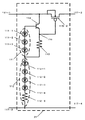
第6の実施の形態は、過充電防止回路を用いた蓄電池制御装置および独立電源系システムに関する。図10に第6の実施の形態の独立電源系システムを示す。 The sixth embodiment relates to a storage battery control device and an independent power supply system using an overcharge prevention circuit. FIG. 10 shows an independent power supply system according to the sixth embodiment.
第6の実施の形態の独立電源系システムでは、蓄電池2に、逆電流防止ダイオード24、過充電防止回路21を介して発電装置1が接続され、機械的スイッチ23を介して負荷3が接続されている。過充電防止回路21、逆電流防止ダイオード24、機械的スイッチ23が蓄電池制御装置11を構成する。すなわち、蓄電池制御装置11に発電装置1、蓄電池2、負荷3が接続されている。尚、逆電流防止ダイオード24は、蓄電池2と過充電防止回路21の間でも、発電装置1と過充電防止回路21の間でもよいものとする。また、逆電流防止ダイオード24は、蓄電池制御装置11の内部にあっても外部にあってもよいものとする。逆電流防止ダイオード24は、発電装置1と一体になっていてもよい。
In the independent power supply system of the sixth embodiment, the
発電装置のプラス端子およびマイナス端子に実質的に接続されている系117−1、117−2を発電系、蓄電池のプラス端子およびマイナス端子に実質的に接続されている系117−3、117−4を蓄電系、負荷のプラス端子およびマイナス端子に実質的に接続されている系117−5、117−6を出力系とする。117−2と117−4と117−6は短絡しているが、説明の都合上別のノードであるとして説明する。実質的に接続されるとは、間にヒューズ、スイッチ、抵抗器、ダイオード、電流計等が間に挿入されている場合も含めて接続されていることを意味する。。 The systems 117-1 and 117-2 that are substantially connected to the plus terminal and the minus terminal of the power generation apparatus are connected to the systems 117-3 and 117 − that are substantially connected to the power generation system and the plus and minus terminals of the storage battery.
発電装置1には、自然エネルギーを利用したものが適する。特に太陽電池などが適する。蓄電池2には鉛蓄電池を用いることができる。図11に、発電装置1に太陽電池を、蓄電池2に鉛蓄電池を用いた場合の例を示す。以下では、発電装置1に太陽電池を、蓄電池2に鉛蓄電池を用いた場合について説明する。 For the
第6の実施の形態の独立電源系システムでは、鉛蓄電池2−1に、逆電流防止ダイオード24、過充電防止回路21を介して太陽電池1−1が接続され、機械的スイッチ23を介して負荷3が接続されている。過充電防止回路21、逆電流防止ダイオード24、機械的スイッチ23が蓄電池制御装置11を構成する。すなわち、蓄電池制御装置11に太陽電池1−1、鉛蓄電池2−1、負荷3が接続されている。尚、逆電流防止ダイオード24は、鉛蓄電池2−1と過充電防止回路21の間でも、太陽電池1−1と過充電防止回路21の間でもよいものとする。また、逆電流防止ダイオード24は、蓄電池制御装置11の内部にあっても外部にあってもよいものとする。逆電流防止ダイオード24は、太陽電池1−1と一体になっていてもよい。 In the independent power supply system of the sixth embodiment, the solar battery 1-1 is connected to the lead storage battery 2-1 via the reverse
図12に過充電防止回路21の内部を記載した回路図を示す。過充電防止回路21の内部は、第1の実施の形態および図2で説明した。ここで図2におけるスイッチング素子115は、PMOSトランジスタを用いることができる。スイッチング素子115に、PMOSトランジスタを用いた場合の過充電防止回路21の内部は図3で示される。図3中の回路部位111は少なくとも1つの発光ダイオードまたはツェナーダイオードを含む。図3では、回路部位111は緑色発光ダイオード111−1、111−2、111−3の直列接続の例が示されている。過充電防止回路21の内部は、第1の実施の形態および図2、図3で説明したため、詳細の説明は割愛する。
FIG. 12 is a circuit diagram showing the inside of the
発電時は、太陽電池1−1のプラスマイナス端子間の電圧は、鉛蓄電池2−1のプラスマイナス間の電圧よりやや高い状態を維持する。太陽電池1−1のプラスマイナス端子間の電圧が第一の一定電圧値を超えるとダイオード群を含む回路部位111に流れる電流が一定値を超え、ノード116の電位が一定値を超え、PMOSトランジスタ115−2はソースドレイン間の抵抗が一定値を超える。その結果、太陽電池1−1のプラスマイナス端子間の電圧がますます上昇し、PMOSトランジスタ115−2はソースドレイン間の抵抗がますます上昇するという正帰還がかかる。そのため、太陽電池1−1のプラスマイナス端子間の電圧は一気に上昇し、PMOSトランジスタ115−2は完全にオフになる。こうなることにより、太陽電池のプラスマイナス端子間の電圧が第一の一定電圧値を超えるとPMOSトランジスタ115−2がオフし、発電系と蓄電系すなわち、太陽電池1−1と鉛蓄電池2−1を切り離すことにより、鉛蓄電池2−1のプラスマイナス端子間の電圧を一定電圧値以上に上げない機能が実現する。すなわち過充電防止機能が実現する。 At the time of power generation, the voltage between the plus and minus terminals of the solar battery 1-1 is kept slightly higher than the voltage between the plus and minus terminals of the lead storage battery 2-1. When the voltage between the positive and negative terminals of the solar cell 1-1 exceeds the first constant voltage value, the current flowing through the
また発電系と蓄電系が切り離された状態では、太陽電池1−1のプラスマイナス端子間の電圧は、太陽電池の開放電圧以下の範囲で高い電圧となる。回路部位111、112の少なくとも片方に発光ダイオードを用いた場合では発電系と蓄電系が切り離された状態では発光ダイオードがある程度の明るさで発光するため、目視により確認することができる。抵抗器112−5により、この時流れる電流を制限することができる。抵抗器112−5の抵抗値は、数百Ω〜数kΩが適する。この抵抗器112−5により電流を制限することにより、ダイオードは電流容量の小さいものを用いることができ、回路、装置、システムの大きさを小さくでき、価格を抑えることができる。
In the state where the power generation system and the power storage system is disconnected, the voltage between the plus and minus terminals of the solar cell 1 -1, a high voltage in the range of the open-circuit voltage below the solar cell. When a light emitting diode is used for at least one of the
発電系と蓄電系すなわち、太陽電池1−1と鉛蓄電池2−1を切り離す基準の一定電圧値は、例えば13.2Vである。 Power system and the power storage system that is, a constant voltage of the reference disconnecting the solar cell 1 -1 and lead-acid battery 2 -1 is, for example, 13.2V.
機械的スイッチ23は、負荷に電流を供給するかどうかを決めるスイッチであり、無くてもよい。負荷は、例えば照明などである。 The
夜になると、太陽電池1−1に太陽光が当たらなくなり、太陽電池1−1のプラスマイナス端子間の電圧は、過充電の判定基準の電圧より十分小さい電圧となる。そのため、負荷3で消費された電流により鉛蓄電池2−1のプラスマイナス端子間の電圧が下がっていたら、翌日に日が昇ると同時に鉛蓄電池2−1へ充電を開始する。太陽電池1のプラス端子117−1と鉛蓄電池2−1のプラス端子117−3の間にバイパススイッチを導入してもよい。このバイパススイッチが一時的にオンすると、同様に鉛蓄電池2のプラスマイナス端子間の電圧が過充電防止の判定基準電圧以下であったら充電を開始する。
At night, sunlight does not hit the solar cell 1-1, and the voltage between the plus and minus terminals of the solar cell 1-1 becomes sufficiently lower than the voltage of the overcharge determination criterion. Therefore, if the voltage between the positive and negative terminals of the lead storage battery 2-1 is reduced by the current consumed by the
逆電流防止ダイオード24の働きにより、鉛蓄電池2−1に蓄えられていた電力が夜間に太陽電池1−1の内部を通って逆方向に流出するということはない。逆電流防止ダイオード24が、鉛蓄電池2−1と過充電防止回路21の間にある構成の場合、発電および蓄電しない夜間の過充電防止回路21の消費電流はさらに小さく抑えることができる。 By the action of the reverse
第6の実施の形態により、過充電を気にせず使用できる、安価で、電力利用効率のよい小規模な独立電源システムを実現することができる。
[第6の実施の形態の変形例]
According to the sixth embodiment, it is possible to realize a small-scale independent power supply system that can be used without worrying about overcharging and that is inexpensive and has high power utilization efficiency.
[Modification of Sixth Embodiment]
第6の実施の形態の変形例は、回路部位111、112にツェナーダイオードを用いている点のみが異なる。 The modification of the sixth embodiment is different only in that Zener diodes are used for the
過充電防止回路21の内部は、第2の実施の形態および図5で説明した通りである。ここで図5におけるスイッチング素子115は、PMOSトランジスタを用いた場合の図である。図5中の回路部位111は少なくとも1つの発光ダイオードまたはツェナーダイオードを含む。図5は、回路部位111が緑色発光ダイオード111−1とツェナーダイオード111−5の直列接続の場合の例である。
The inside of the
第6の実施の形態の変形例の動作および原理は、元の第6の実施の形態と同様である。
[第7の実施の形態]The operation and principle of the modified example of the sixth embodiment are the same as those of the original sixth embodiment.
[Seventh Embodiment]
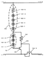
第7の実施の形態は、過充電防止回路および過放電防止回路を用いた蓄電池制御装置および独立電源システムに関する。図13に第7の実施の形態の独立電源システムを示す。 The seventh embodiment relates to a storage battery control device and an independent power supply system using an overcharge prevention circuit and an overdischarge prevention circuit. FIG. 13 shows an independent power supply system according to the seventh embodiment.
第7の実施の形態の独立電源系システムでは、蓄電池2に、過充電防止回路21、逆電流防止ダイオード24を介して発電装置1が接続され、機械的スイッチ23および過放電防止回路22を介して負荷が接続されている。過充電防止回路21、過放電防止回路22、逆電流防止ダイオード24、機械的スイッチ23が蓄電池制御装置11を構成する。すなわち、蓄電池制御装置11に発電装置1、蓄電池2、負荷3が接続されている。 In the independent power supply system of the seventh embodiment, the
尚、逆電流防止ダイオード24は、蓄電池2と過充電防止回路21の間でも、発電装置1と過充電防止回路21の間でもよいものとする。また、逆電流防止ダイオード24は、蓄電池制御装置11の内部にあっても外部にあってもよいものとする。逆電流防止ダイオード24は、発電装置1と一体になっていてもよい。 The reverse
発電装置のプラス端子およびマイナス端子に実質的に接続されている系117−1、117−2を発電系、蓄電池のプラス端子およびマイナス端子に実質的に接続されている系117−3、117−4を蓄電系、負荷のプラス端子およびマイナス端子に実質的に接続されている系117−5、117−6を出力系とする。117−2と117−4と117−6は短絡しているが、説明の都合上別のノードであるとして説明する。実質的に接続されるとは、間にヒューズ、スイッチ、抵抗器、ダイオード、電流計等が間に挿入されている場合も含めて接続されていることを意味する。
The systems 117-1 and 117-2 that are substantially connected to the plus terminal and the minus terminal of the power generation apparatus are connected to the systems 117-3 and 117 − that are substantially connected to the power generation system and the plus and minus terminals of the storage battery.
発電装置1には、自然エネルギーを利用したものが適する。特に太陽電池などが適する。蓄電池2には鉛蓄電池を用いることができる。図14に、発電装置1に太陽電池を、蓄電池2に鉛蓄電池を用いた場合の例を示す。以下では、発電装置1に太陽電池を、蓄電池2に鉛蓄電池を用いた場合について説明する。 For the
第7の実施の形態の独立電源システムでは、鉛蓄電池2−1に、過充電防止回路21、逆電流防止ダイオード24を介して太陽電池1−1が接続され、機械的スイッチ23および過放電防止回路22を介して負荷3が接続されている。過充電防止回路21、過放電防止回路22、逆電流防止ダイオード24、機械的スイッチ23が蓄電池制御装置11を構成する。すなわち、蓄電池制御装置11に太陽電池1−1、鉛蓄電池2−1、負荷3が接続されている。
In the independent power supply system of the seventh embodiment, the solar battery 1-1 is connected to the lead storage battery 2-1 via the
図15に過充電防止回路21、過放電防止回路22の内部を記載した回路図を示す。過充電防止回路21の内部は、第1の実施の形態および図2、図3で説明したため、詳細の説明は割愛する。過放電防止回路22の内部は、第5の実施の形態および図8で説明したため、詳細の説明は割愛する。 FIG. 15 is a circuit diagram showing the inside of the
発電時は、太陽電池1−1のプラスマイナス端子間の電圧は、鉛蓄電池2−1のプラスマイナス間の電圧よりやや高い状態を維持する。太陽電池1−1のプラスマイナス端子間の電圧が第一の一定電圧値を超えるとダイオード群を含む回路部位111に流れる電流が一定値を超え、ノード116の電位が一定値を超え、PMOSトランジスタ115−2はソースドレイン間の抵抗が一定値を超える。その結果、太陽電池1−1のプラスマイナス端子間の電圧がますます上昇し、PMOSトランジスタ115−2はソースドレイン間の抵抗がますます上昇するという正帰還がかかる。そのため、太陽電池1−1のプラスマイナス端子間の電圧は一気に上昇し、PMOSトランジスタ115−2は完全にオフになる。こうなることにより、太陽電池1−1のプラスマイナス端子間の電圧が第一の一定電圧値を超えるとPMOSトランジスタ115−2がオフし、発電系と蓄電系すなわち、太陽電池1−1と鉛蓄電池2−1を切り離すことにより、鉛蓄電池2−1のプラスマイナス端子間の電圧を第一の一定電圧値以上に上げない機能が実現する。すなわち過充電防止機能が実現する。
At the time of power generation, the voltage between the plus and minus terminals of the solar battery 1-1 is kept slightly higher than the voltage between the plus and minus terminals of the lead storage battery 2-1. When the voltage between the positive and negative terminals of the solar cell 1-1 exceeds the first constant voltage value, the current flowing through the
また発電系と蓄電系が切り離された状態では、太陽電池1−1のプラスマイナス端子間の電圧は、太陽電池の開放電圧以下の範囲で高い電圧となる。回路部位111、112の少なくとも片方に発光ダイオードを用いた場合では発電系と蓄電系が切り離された状態では発光ダイオードがある程度の明るさで発光するため、目視により確認することができる。抵抗器112−5により、この時流れる電流を制限することができる。抵抗器112−5の抵抗値は、数百Ω〜数kΩが適する。この抵抗器112−5により電流を制限することにより、ダイオードは電流容量の小さいものを用いることができ、回路、装置、システムの大きさを小さくでき、価格を抑えることができる。
In the state where the power generation system and the power storage system is disconnected, the voltage between the plus and minus terminals of the solar cell 1 -1, a high voltage in the range of the open-circuit voltage below the solar cell. When a light emitting diode is used for at least one of the
発電系と蓄電系すなわち、太陽電池1−1と鉛蓄電池2−1を切り離す基準の一定電圧値は、例えば13.2Vである。 Power system and the power storage system that is, a constant voltage of the reference disconnecting the solar cell 1 -1 and lead-acid battery 2 -1 is, for example, 13.2V.
機械的スイッチ23は、負荷に電流を供給するかどうかを決めるスイッチであり、無くてもよい。負荷は、例えば照明などである。 The
鉛蓄電池2−1のプラスマイナス端子間の電圧が第二の一定電圧値を下回るとダイオード群を含む回路部位131に流れる電流が一定値を下回り、ノード136の電位が一定値を下回り、ノード139の電位が一定値を超え、PMOSトランジスタ135−2はソースドレイン間の抵抗が一定値を超える。PMOSトランジスタ137および抵抗器138による増幅段により、蓄電系のプラスマイナス端子間の電圧の僅かな減少によりPMOSトランジスタ135−2のソースドレイン間の抵抗を大幅に上昇させることができる。このことにより、蓄電系のプラスマイナス端子間の電圧が第二の一定電圧値以下になると出力系と蓄電系を切り離すことにより、蓄電系のプラスマイナス端子間の電圧を第二の一定電圧値以下に下げない機能が実現する。すなわち過放電防止機能が実現する。 When the voltage between the positive and negative terminals of the lead-acid battery 2-1 falls below the second constant voltage value, the current flowing through the
蓄電系と出力系すなわち、鉛蓄電池2−1と負荷3を切り離す基準の第二の一定電圧値は、例えば11.2Vである。第一の一定電圧値は、第二の一定電圧値より必ず高く設計する。第一の一定電圧値を、第二の一定電圧値と異なる値にするには、回路部位111と回路部位131の電圧降下量を変えるか、あるいは、回路部位112と回路部位132の電圧降下量を変える方法がある。例えば、回路部位112では緑色発光ダイオード4つの直列接続を用いるのに対し、回路部位132では緑色発光ダイオード2つと赤色発光ダイオード2つの直列接続を用いるなどの方法が可能である。尚、過放電防止機能により出力系と蓄電系が切り離されると、電力会社の系統から電力が供給されるようにしてもよい。
Output power storage system based Namely, the second predetermined voltage of the reference disconnecting the lead-acid battery 2 -1 and the
夜になると、太陽電池1−1に太陽光が当たらなくなり、太陽電池1−1のプラスマイナス端子間の電圧は、過充電の判定基準の電圧より十分小さい電圧となる。そのため、負荷3で消費された電流により鉛蓄電池2−1のプラスマイナス端子間の電圧が下がっていたら、翌日に日が昇ると同時に鉛蓄電池2−1へ充電を開始する。太陽電池1−1のプラス端子117−1と鉛蓄電池2−1のプラス端子117−3の間にバイパススイッチを導入してもよい。このバイパススイッチが一時的にオンすると、同様に鉛蓄電池2のプラスマイナス端子間の電圧が過充電防止の判定基準電圧以下であったら充電を開始する。一方、鉛蓄電池2−1のプラスマイナス端子間の電圧が戻り次第、鉛蓄電池2−1と負荷3の接続は再開される。
At night, sunlight does not hit the solar cell 1-1, and the voltage between the plus and minus terminals of the solar cell 1-1 becomes sufficiently lower than the voltage of the overcharge determination criterion. Therefore, if the voltage between the positive and negative terminals of the lead storage battery 2-1 is reduced by the current consumed by the
逆電流防止ダイオード24の働きにより、鉛蓄電池2−1に蓄えられていた電力が夜間に太陽電池1−1の内部を通って逆方向に流出するということはない。逆電流防止ダイオード24が、鉛蓄電池2−1と過充電防止回路21の間にある構成の場合、発電および蓄電しない夜間の過充電防止回路21の消費電流はさらに小さく抑えることができる。 By the action of the reverse
第7の実施の形態により、過充電、過放電を気にせず使用できる、安価で電力利用効率のよい小規模な独立電源システムを実現することができる。
(産業上の利用可能性)
According to the seventh embodiment, it is possible to realize a small-scale independent power supply system that can be used without worrying about overcharge and overdischarge and that is inexpensive and has high power utilization efficiency.
(Industrial applicability)
例えば送電コストの大きい山間部における夜間に点灯する道路標識、案内標識、看板向けの電源システムに用いることができる。また、太陽電池と過充電防止回路にて、長期間自動車に乗らないときにバッテリーがあがらないようにするための製品に用いることができる。 For example, the present invention can be used in a power system for road signs, guide signs, and signboards that are lit at night in mountainous areas where power transmission costs are high. In addition, the solar battery and the overcharge prevention circuit can be used for a product for preventing the battery from rising when the vehicle is not taken for a long time.
1 発電装置
2 蓄電池
1−1 太陽電池
2−1 鉛蓄電池
3 負荷
11 蓄電池制御装置
21 過充電防止回路
22 過放電防止回路
23 機械的スイッチ
24 逆電流防止ダイオード
111、112、121、122、131、132 回路部位
111−1、111−2、111−3、112−1、112−2、112−3、112−4、121−1、121−2、121−3、122−1、122−2、122−3,122−4、131−1、131−2、131−3、132−1、132−2 緑色発光ダイオード
112−8、132−3、132−4 赤色発光ダイオード
112−9、112−10 シリコンダイオード
112−11、112−12、112−13、112−14 スイッチ
111−5、112−6、112−7 ツェナーダイオード
112−5、122−5、132−5、113、123、133、138 抵抗器
114、134 PNP型バイポーラトランジスタ
124 NPN型バイポーラトランジスタ
115、135 スイッチング素子
115−2、135−2、137 PMOSトランジスタ
125−2 NMOSトランジスタ
116、126、136、139 ノード
117−1 発電系のプラス端子
117−2 発電系のマイナス端子
117−3 蓄電系のプラス端子
117−4 蓄電系のマイナス端子
117−5 出力系のプラス端子
117−6 出力系のマイナス端子DESCRIPTION OF SYMBOLS 1 Power generator 2 Storage battery 1-1 Solar battery 2-1 Lead storage battery 3 Load 11 Storage battery control apparatus 21 Overcharge prevention circuit 22 Overdischarge prevention circuit 23 Mechanical switch 24 Reverse current prevention diode 111,112,121,122,131, 132 Circuit parts 111-1, 111-2, 111-3, 112-1, 112-2, 112-3, 112-4, 121-1, 121-2, 121-3, 122-1, 122-2 122-3, 122-4, 131-1, 131-2, 131-3, 132-1, 132-2 Green light emitting diode 112-8, 132-3, 132-4 Red light emitting diode 112-9, 112 -10 Silicon diode 112-11, 112-12, 112-13, 112-14 Switch 111-5, 112-6, 112-7 Zener diode 1 12-5, 122-5, 132-5, 113, 123, 133, 138 Resistor 114, 134 PNP bipolar transistor 124 NPN bipolar transistor 115, 135 Switching element 115-2, 135-2, 137 PMOS transistor 125 -2 NMOS transistors 116, 126, 136, 139 Node 117-1 Power system positive terminal 117-2 Power system negative terminal 117-3 Power storage system positive terminal 117-4 Power storage system negative terminal 117-5 Positive terminal 117-6 Negative terminal of output system
Claims (19)
の一端に実質的に接続され、もう一端は発電装置のマイナスの系統および蓄電池のマイナスの系統に実質的に接続され、前記抵抗器の一端は、前記第一の回路部位の一端および前記第二の回路部位の一端に実質的に接続され、もう一端は前記第一のPNP型バイポーラトランジスタのエミッタおよび前記第一のPMOSトランジスタのゲートに実質的に接続され、前記第一のPMOSトランジスタのソースは発電装置のプラスの系統に実質的に接続され、ゲートは前記第一のPNP型バイポーラトランジスタのエミッタおよび前記抵抗器の一端に実質的に接続され、ドレインは蓄電池のプラスの系統に実質的に接続され、前
記第一の回路部位は少なくとも一つのダイオードを含み、前記第二の回路部位は少なくとも一つのダイオードを含むことを特徴とする回路。 The first PNP type bipolar transistor, the first circuit part, the second circuit part, the resistor, and the first PMOS transistor are included, and the collector of the first PNP type bipolar transistor is a plus of the power generator. In this system, the base is substantially connected to one end of the first circuit portion, the emitter is substantially connected to one end of the resistor and the gate of the first PMOS transistor, and one end of the first circuit portion is connected to the first circuit portion. The other end of the PNP bipolar transistor is substantially connected to one end of the second circuit portion and one end of the resistor, and one end of the second circuit portion is one end of the first circuit portion. And substantially connected to one end of the resistor, and the other end is substantially connected to the negative system of the generator and the negative system of the storage battery, One end of the resistor is substantially connected to one end of the first circuit portion and one end of the second circuit portion, and the other end is an emitter of the first PNP-type bipolar transistor and the first PMOS. Substantially connected to the gate of the transistor, the source of the first PMOS transistor is substantially connected to the positive system of the generator, and the gate is the emitter of the first PNP-type bipolar transistor and one end of the resistor. The drain is substantially connected to the positive battery system, the first circuit portion includes at least one diode, and the second circuit portion includes at least one diode. Features circuit.
抗器の一端に実質的に接続され、もう一端は発電装置のプラスの系統および蓄電池のプラスの系統に実質的に接続され、前記抵抗器の一端は、前記第一の回路部位の一端および前記第二の回路部位の一端に実質的に接続され、もう一端は前記第一のNPN型バイポーラトランジスタのコレクタおよび前記第一のNMOSトランジスタのゲートに実質的に接続され、前記第一のNMOSトランジスタのソースは発電装置のマイナスの系統に実質的に接続され、ゲートは前記第一のNPN型バイポーラトランジスタのコレクタおよび前記抵抗器の一端に実質的に接続され、ドレインは蓄電池のマイナスの系統に実質的に接続され
、前記第一の回路部位は少なくとも一つのダイオードを含み、前記第二の回路部位は少なくとも一つのダイオードを含むことを特徴とする回路。 The first NPN type bipolar transistor, the first circuit part, the second circuit part, the resistor, and the first NMOS transistor are provided, and the emitter of the first NPN type bipolar transistor is the minus of the power generator. In this system, the base is substantially connected to one end of the first circuit portion, the collector is substantially connected to one end of the resistor and the gate of the first NMOS transistor, and one end of the first circuit portion is connected to the first circuit portion. The base of one NPN type bipolar transistor, the other end is substantially connected to one end of the second circuit portion and one end of the resistor, and one end of the second circuit portion is connected to the first circuit portion. One end substantially connected to one end of the resistor and the other end substantially connected to the positive system of the generator and the positive system of the storage battery; One end of the resistor is substantially connected to one end of the first circuit portion and one end of the second circuit portion, and the other end is a collector of the first NPN-type bipolar transistor and the first NMOS. Substantially connected to the gate of the transistor, the source of the first NMOS transistor is substantially connected to the negative system of the generator, and the gate is the collector of the first NPN-type bipolar transistor and one end of the resistor And the drain is substantially connected to the negative system of the storage battery, the first circuit portion includes at least one diode, and the second circuit portion includes at least one diode. Features circuit.
A first current flowing through a first diode or a plurality of diodes connected in series is amplified and copied by a bipolar transistor to form a second current including a power generation device and a storage battery, and the second current is used as a resistive load. The first voltage is converted into a first voltage, and the first switching element is turned on / off using the first voltage. The first current and the second current are a second one diode or A plurality of diodes connected in series, wherein the first one diode or the plurality of diodes connected in series uses a control circuit existing on the power generator side of the first switching element, and the power generator When the voltage at both ends of the system exceeds a certain voltage value, the current flowing through the first diode or the plurality of diodes connected in series increases, and the first switch Independent power supply system, characterized in that system and system of the battery of the power generating device is disconnected by the ring element is turned off.
The independent power supply system according to claim 18 , wherein the power generation device is a solar battery.
Priority Applications (2)
| Application Number | Priority Date | Filing Date | Title |
|---|---|---|---|
| JP2010132445A JP5130429B2 (en) | 2010-05-23 | 2010-05-23 | Storage battery control circuit, storage battery control device, and independent power system |
| US13/064,827 US20110285354A1 (en) | 2010-05-23 | 2011-04-20 | Rechargeable battery controlling circuit, rechargeable battery controlling device, independent power system and battery pack |
Applications Claiming Priority (1)
| Application Number | Priority Date | Filing Date | Title |
|---|---|---|---|
| JP2010132445A JP5130429B2 (en) | 2010-05-23 | 2010-05-23 | Storage battery control circuit, storage battery control device, and independent power system |
Publications (3)
| Publication Number | Publication Date |
|---|---|
| JP2011250665A JP2011250665A (en) | 2011-12-08 |
| JP2011250665A5 JP2011250665A5 (en) | 2012-02-16 |
| JP5130429B2 true JP5130429B2 (en) | 2013-01-30 |
Family
ID=45415203
Family Applications (1)
| Application Number | Title | Priority Date | Filing Date |
|---|---|---|---|
| JP2010132445A Expired - Fee Related JP5130429B2 (en) | 2010-05-23 | 2010-05-23 | Storage battery control circuit, storage battery control device, and independent power system |
Country Status (1)
| Country | Link |
|---|---|
| JP (1) | JP5130429B2 (en) |
Families Citing this family (2)
| Publication number | Priority date | Publication date | Assignee | Title |
|---|---|---|---|---|
| JP5495217B1 (en) * | 2013-09-14 | 2014-05-21 | 拓 岩佐 | Overcharge prevention circuit, overdischarge prevention circuit, storage battery control device, independent power supply system and battery pack |
| JP6817892B2 (en) * | 2017-05-17 | 2021-01-20 | 株式会社Nttドコモ | DC power supply system |
Family Cites Families (4)
| Publication number | Priority date | Publication date | Assignee | Title |
|---|---|---|---|---|
| JPH08140273A (en) * | 1994-11-08 | 1996-05-31 | Fujitsu Ltd | Load short-circuit protective circuit |
| JP3322542B2 (en) * | 1995-11-30 | 2002-09-09 | 三洋電機株式会社 | Charging circuit |
| JPH10243574A (en) * | 1997-02-25 | 1998-09-11 | Tdk Corp | Power supply part, photovoltaic generator provided with this power supply part and photovoltaic application system using this photovolatic generator |
| JP4090670B2 (en) * | 2000-06-09 | 2008-05-28 | ニチコン株式会社 | Battery protection circuit |
-
2010
- 2010-05-23 JP JP2010132445A patent/JP5130429B2/en not_active Expired - Fee Related
Also Published As
| Publication number | Publication date |
|---|---|
| JP2011250665A (en) | 2011-12-08 |
Similar Documents
| Publication | Publication Date | Title |
|---|---|---|
| JP5076024B2 (en) | Storage system that maximizes the use of renewable energy | |
| US20110285354A1 (en) | Rechargeable battery controlling circuit, rechargeable battery controlling device, independent power system and battery pack | |
| CN101582594B (en) | Charging control circuit | |
| US20080169784A1 (en) | Solar power system | |
| JP2013529455A (en) | Advanced storage battery system | |
| KR101147205B1 (en) | Apparatus and method of controlling high current, and power storage apparatus using the same | |
| CN104410139B (en) | Battery of battery-driven truck is full of automatic power-off circuit and auto-power-off device | |
| US20120261992A1 (en) | Renewable Energy Power Controller | |
| WO2022033002A1 (en) | Photovoltaic power generation system | |
| CN204598407U (en) | There is the switching circuit of emergency starting function power device | |
| JP5130429B2 (en) | Storage battery control circuit, storage battery control device, and independent power system | |
| JP2011147203A (en) | Overcharge protection device of charging battery | |
| CN206524663U (en) | A kind of BMS charging switch protecting circuits | |
| JP2007288932A (en) | Charge control device of photovoltaic power generation facility | |
| JP5495217B1 (en) | Overcharge prevention circuit, overdischarge prevention circuit, storage battery control device, independent power supply system and battery pack | |
| CN104184128A (en) | Battery discharge protection method and circuit and lamp thereof | |
| JP2017127173A (en) | Power storage device | |
| WO2012133186A1 (en) | Switch circuit control unit, and charging and discharging system | |
| JP2012115028A (en) | Storage battery control device and independent power supply system | |
| WO2013046658A1 (en) | Switching apparatus and power storage system | |
| JP2015073377A (en) | Solar cell power supply device | |
| US10826320B2 (en) | Solar power system | |
| CN102148524A (en) | Charger | |
| KR20150059222A (en) | Solar power storage apparatus and method therefor | |
| JP2011250665A5 (en) |
Legal Events
| Date | Code | Title | Description |
|---|---|---|---|
| A521 | Written amendment |
Free format text: JAPANESE INTERMEDIATE CODE: A523 Effective date: 20111220 |
|
| A621 | Written request for application examination |
Free format text: JAPANESE INTERMEDIATE CODE: A621 Effective date: 20111220 |
|
| A871 | Explanation of circumstances concerning accelerated examination |
Free format text: JAPANESE INTERMEDIATE CODE: A871 Effective date: 20111220 |
|
| A975 | Report on accelerated examination |
Free format text: JAPANESE INTERMEDIATE CODE: A971005 Effective date: 20120119 |
|
| A131 | Notification of reasons for refusal |
Free format text: JAPANESE INTERMEDIATE CODE: A131 Effective date: 20120410 |
|
| A521 | Written amendment |
Free format text: JAPANESE INTERMEDIATE CODE: A523 Effective date: 20120508 |
|
| A131 | Notification of reasons for refusal |
Free format text: JAPANESE INTERMEDIATE CODE: A131 Effective date: 20120703 |
|
| A521 | Written amendment |
Free format text: JAPANESE INTERMEDIATE CODE: A523 Effective date: 20120712 |
|
| A01 | Written decision to grant a patent or to grant a registration (utility model) |
Free format text: JAPANESE INTERMEDIATE CODE: A01 Effective date: 20120821 |
|
| A01 | Written decision to grant a patent or to grant a registration (utility model) |
Free format text: JAPANESE INTERMEDIATE CODE: A01 |
|
| A61 | First payment of annual fees (during grant procedure) |
Free format text: JAPANESE INTERMEDIATE CODE: A61 Effective date: 20120825 |
|
| FPAY | Renewal fee payment (event date is renewal date of database) |
Free format text: PAYMENT UNTIL: 20171116 Year of fee payment: 5 |
|
| R150 | Certificate of patent or registration of utility model |
Free format text: JAPANESE INTERMEDIATE CODE: R150 |
|
| LAPS | Cancellation because of no payment of annual fees |