JP4029709B2 - Power converter - Google Patents
Power converter Download PDFInfo
- Publication number
- JP4029709B2 JP4029709B2 JP2002284619A JP2002284619A JP4029709B2 JP 4029709 B2 JP4029709 B2 JP 4029709B2 JP 2002284619 A JP2002284619 A JP 2002284619A JP 2002284619 A JP2002284619 A JP 2002284619A JP 4029709 B2 JP4029709 B2 JP 4029709B2
- Authority
- JP
- Japan
- Prior art keywords
- phase
- power
- output
- inverter
- voltage
- Prior art date
- Legal status (The legal status is an assumption and is not a legal conclusion. Google has not performed a legal analysis and makes no representation as to the accuracy of the status listed.)
- Expired - Fee Related
Links
Images


Classifications
-
- H—ELECTRICITY
- H02—GENERATION; CONVERSION OR DISTRIBUTION OF ELECTRIC POWER
- H02M—APPARATUS FOR CONVERSION BETWEEN AC AND AC, BETWEEN AC AND DC, OR BETWEEN DC AND DC, AND FOR USE WITH MAINS OR SIMILAR POWER SUPPLY SYSTEMS; CONVERSION OF DC OR AC INPUT POWER INTO SURGE OUTPUT POWER; CONTROL OR REGULATION THEREOF
- H02M7/00—Conversion of ac power input into dc power output; Conversion of dc power input into ac power output
- H02M7/42—Conversion of dc power input into ac power output without possibility of reversal
- H02M7/44—Conversion of dc power input into ac power output without possibility of reversal by static converters
- H02M7/48—Conversion of dc power input into ac power output without possibility of reversal by static converters using discharge tubes with control electrode or semiconductor devices with control electrode
- H02M7/483—Converters with outputs that each can have more than two voltages levels
- H02M7/4835—Converters with outputs that each can have more than two voltages levels comprising two or more cells, each including a switchable capacitor, the capacitors having a nominal charge voltage which corresponds to a given fraction of the input voltage, and the capacitors being selectively connected in series to determine the instantaneous output voltage
-
- H—ELECTRICITY
- H02—GENERATION; CONVERSION OR DISTRIBUTION OF ELECTRIC POWER
- H02M—APPARATUS FOR CONVERSION BETWEEN AC AND AC, BETWEEN AC AND DC, OR BETWEEN DC AND DC, AND FOR USE WITH MAINS OR SIMILAR POWER SUPPLY SYSTEMS; CONVERSION OF DC OR AC INPUT POWER INTO SURGE OUTPUT POWER; CONTROL OR REGULATION THEREOF
- H02M1/00—Details of apparatus for conversion
- H02M1/0095—Hybrid converter topologies, e.g. NPC mixed with flying capacitor, thyristor converter mixed with MMC or charge pump mixed with buck
-
- H—ELECTRICITY
- H02—GENERATION; CONVERSION OR DISTRIBUTION OF ELECTRIC POWER
- H02M—APPARATUS FOR CONVERSION BETWEEN AC AND AC, BETWEEN AC AND DC, OR BETWEEN DC AND DC, AND FOR USE WITH MAINS OR SIMILAR POWER SUPPLY SYSTEMS; CONVERSION OF DC OR AC INPUT POWER INTO SURGE OUTPUT POWER; CONTROL OR REGULATION THEREOF
- H02M7/00—Conversion of ac power input into dc power output; Conversion of dc power input into ac power output
- H02M7/42—Conversion of dc power input into ac power output without possibility of reversal
- H02M7/44—Conversion of dc power input into ac power output without possibility of reversal by static converters
- H02M7/48—Conversion of dc power input into ac power output without possibility of reversal by static converters using discharge tubes with control electrode or semiconductor devices with control electrode
- H02M7/483—Converters with outputs that each can have more than two voltages levels
- H02M7/487—Neutral point clamped inverters
-
- H—ELECTRICITY
- H02—GENERATION; CONVERSION OR DISTRIBUTION OF ELECTRIC POWER
- H02M—APPARATUS FOR CONVERSION BETWEEN AC AND AC, BETWEEN AC AND DC, OR BETWEEN DC AND DC, AND FOR USE WITH MAINS OR SIMILAR POWER SUPPLY SYSTEMS; CONVERSION OF DC OR AC INPUT POWER INTO SURGE OUTPUT POWER; CONTROL OR REGULATION THEREOF
- H02M7/00—Conversion of ac power input into dc power output; Conversion of dc power input into ac power output
- H02M7/42—Conversion of dc power input into ac power output without possibility of reversal
- H02M7/44—Conversion of dc power input into ac power output without possibility of reversal by static converters
- H02M7/48—Conversion of dc power input into ac power output without possibility of reversal by static converters using discharge tubes with control electrode or semiconductor devices with control electrode
- H02M7/483—Converters with outputs that each can have more than two voltages levels
- H02M7/49—Combination of the output voltage waveforms of a plurality of converters
Landscapes
- Engineering & Computer Science (AREA)
- Power Engineering (AREA)
- Inverter Devices (AREA)
Description
【0001】
【発明の属する技術分野】
この発明は、複数のインバータを組み合わせて滑らかな交流出力波形を得ることが可能な電力変換器に関するものである。
【0002】
【従来の技術】
従来の3相インバータ装置は、交流電源からトランスを介して入力された交流電力を3相コンバータで整流して直流電力に変換し、その直流電力をコンデンサにて平滑化し、さらにこのコンデンサによる直流電力を3相インバータで交流電力に変換する。
このような従来の3相インバータ装置のインバータ部は、例えばダイオードがそれぞれ逆並列に接続された複数の自己消弧型半導体スイッチング素子で構成され、各半導体スイッチング素子をPWM制御によりオン・オフ制御することで、コンデンサの直流電力を交流電力に変換して出力を得る(例えば、非特許文献1参照)。
【0003】
【非特許文献1】
「半導体電力変換回路」第5版、電気学会発行、オーム社発売、1990年4月10日、p.212−219
【0004】
【発明が解決しようとする課題】
従来の3相インバータ装置は、以上のように構成されてPWM制御にて出力電圧を調整しているため、出力端の電圧変化が大きく、また高調波を抑制するために、図30に示すようにインバータ1の出力側に複雑で大容量の出力フィルタ2が必要であった。このため、装置が大型化すると共に、この出力フィルタ2の電圧降下分だけ3相インバータの皮相電力を増加しておく必要があった。
【0005】
この発明は、上記のような問題点を解消するために成されたものであって、大容量の出力フィルタを必要とせずに滑らかな交流出力波形を得ることが可能で、小型化、低コスト化の促進された電力変換装置の構造を提供することを目的とする。
【0006】
【課題を解決するための手段】
この発明に係る電力変換装置は、
接続される負荷に多相交流で電力を出力する電力変換装置であって、
前記多相交流の各相を構成する複数の各相電力経路と、
前記複数の各相電力経路にそれぞれ交流側が直列に接続される複数の単相インバータと、
前記複数の単相インバータの直流側にそれぞれ接続される複数の各相電力蓄積手段と、
前記複数の各相電力経路に接続される多相インバータと、
前記多相インバータの直流側に接続される直流電源と、
前記複数の単相インバータと前記多相インバータとを制御して、前記複数の各相電力経路を経由して前記負荷に電力を出力させる制御回路と
を備え、
前記複数の単相インバータは、
前記制御回路の制御に基づいて、接続される前記各相電力蓄積手段に蓄積される電力を接続される前記各相電力経路に出力すること、または前記接続される各相電力経路を経由して入力される電力を前記接続される各相電力蓄積手段に蓄積することを可能とし、
前記多相インバータは、
前記制御回路の制御に基づいて、前記直流電源の電力を前記各相電力経路に出力することを可能とし、
前記制御回路は、前記各相電力蓄積手段へ電力を蓄積し、かつ、前記各相電力蓄積手段から電力を出力して、前記複数の各相電力経路における出力電圧が、所定の交流電圧の波形となるように、前記複数の単相インバータと前記多相インバータとを制御すること
としたものである。
【0016】
【発明の実施の形態】
実施の形態1.
以下、この発明の実施の形態1を図について説明する。
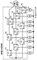
図1は、この発明の実施の形態1による3相負荷駆動用の電力変換器の構成を示す図である。図に示すように、3相電力変換器全体は、各相がスター結線されて3相負荷4に電力供給するもので、それぞれの相は3つの単相インバータであるVaインバータ3a、Vbインバータ3b、Vcインバータ3cを直列接続された単相多重変換器から成る。各単相インバータ3a、3b、3cは、系統からトランス5を通して引き込まれる3相交流電力を整流して直流電力に変換する3相コンバータ部と、その直流電力を平滑するコンデンサと、該コンデンサを直流電源として直流電力を交流電力に変換する単相インバータ部とを備え、上記3相コンバータ部の例を図2に、単相インバータ部の例を図3に示す。
【0017】
図2(a)に示す3相コンバータ部(コンデンサを含む)は、ダイオード整流回路6aと平滑フィルタ(L,C)7aとで構成されるものである。また図2(b)に示す3相コンバータ部(コンデンサを含む)は、サイリスタ整流回路6bと平滑フィルタ(L,C)7aとで構成され、さらに図2(c)に示す3相コンバータ部(コンデンサを含む)は、3相昇圧チョッパ6cとコンデンサフィルタ7cとで構成される。
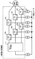
図3(a)〜図3(d)は、単相インバータ部(コンデンサを含む)の4つの構成例を示したもので、ダイオードを逆並列に接続した自己消弧型半導体スイッチング素子でフルブリッジのインバータを構成した。図3(a)、図3(c)では、自己消弧型半導体スイッチング素子にIGBTを用いたものが、図3(b)、図3(d)では、自己消弧型半導体スイッチング素子に、GCTを用いたものが示される。その他、GTO、トランジスタ、MOSFET等のものでも良い。また自己消弧機能がないサイリスタ等でも強制転流動作が可能であれば使用できる。また、図3(c)、図3(d)に示すように、素子を複数個直列に接続してインバータを構成しても良い。
【0018】
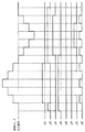
このように構成される単相インバータ(Vaインバータ3a、Vbインバータ3b、Vcインバータ3c)は、それぞれコンデンサに充電される電圧Va、Vb、Vcを電圧源として電圧を出力するが、Va、Vb、Vcの関係は、それぞれ異なる値(Va<Vb<Vc)で、1:2:4、1:3:4、1:3:5、1:3:6、1:3:7、1:3:8、1:3:9のいずれかの関係となる。それぞれの場合について、Vaインバータ3a、Vbインバータ3b、Vcインバータ3cの各インバータの出力論理とそれらを直列接続した単相多重変換器の出力階調(電圧レベル)との関係を図4のA〜Gの論理表に示す。
まず、図4のA表の場合について説明する。
Va、Vb、Vcは、1:2:4の関係で、最小電圧値Vaの2n(n=0,1,2)の関係である。A表に示すように、最下位ビット、中間ビット、最上位ビットの3つの単相インバータ3a、3b、3cの組み合わせにより、これらの発生電圧の総和で0〜7の8階調の出力電圧が得られる。正弦波出力階調を得るための各単相インバータ出力波形を、図5に示す。Va、Vb、Vcが1:2:4の場合は、図5(a)に示されるもので、3つの単相インバータ3a、3b、3cの発生電圧の組み合わせにより、非常に滑らかな出力階調電圧が得られていることがわかる。このため、従来の電力変換器の後段に設けられていた平滑用の出力フィルタ2をなくす、あるいは小さな容量にすることができ、電力変換器を低コスト化、小型化、簡略化できる。
【0019】
次に、図4のB〜G表の場合について説明する。
Va、Vb、Vcは、1:3:4、1:3:5、1:3:6、1:3:7、1:3:8、1:3:9の関係で、各表に示すように、最下位ビット、中間ビット、最上位ビットの3つの単相インバータ3a、3b、3cの組み合わせにより、これらの発生電圧の総和で9階調、10階調、11階調、12階調、13階調、14階調の出力電圧が得られる。これらの場合、単相インバータ3a、3b、3cの発生電圧の中で、単相多重変換器の出力階調の極性と、逆極性のものが存在することがある。例えば、Va、Vb、VcがC表に示す1:3:5の場合、出力階調が1、3、4、5、6、8、9の場合には、それぞれの単相インバータ3a、3b、3cは出力階調の極性と同じ極性に電圧を発生するが、出力階調が2、7の場合にはVaインバータ3aは、逆極性である電圧(−Va)を発生することになる。これは、Vaインバータ3a内のコンデンサが、回生により充電されることを示す。これにより、連続的な出力階調が得られる。
正弦波出力階調を得るための各単相インバータ出力波形で、Va、Vb、Vcが1:3:5の場合は、図5(b)に示されるもので、この場合も3つの単相インバータ3a、3b、3cの発生電圧の組み合わせにより、非常に滑らかな出力階調電圧が得られていることがわかる。このため、平滑用の出力フィルタ2をなくす、あるいは小さな容量にすることができ、電力変換器が低コスト化、小型化、簡略化できる。
他のB、D〜G表の場合も同様に、非常に滑らかな出力階調電圧が得られ、平滑用の出力フィルタ2を不要化、あるいは小型化でき、電力変換器が低コスト化、小型化、簡略化できる。
【0020】
実施の形態2.
図6は、この発明の実施の形態2による3相電力変換器の構成を示す図である。図に示すように、上記実施の形態1で示した3相電力変換器の最下位ビットのVaインバータ3aの出力に個別のフィルタ8を接続する。
図7は、Vaインバータ3aとフィルタ8との構成例、および最下位ビットのVaインバータ3aの出力波形とそれがフィルタ8で平滑化された出力波形を示す。図に示すように、Vaインバータ3aの出力にL,Cからなるフィルタ8を接続する。さらに、このように出力フィルタ8を備えた最下位ビットのVaインバータ3aをPWM制御あるいはチョッパ制御により出力パルス幅を制御して動作させる。PWM制御あるいはチョッパ制御により動作させたVaインバータ3aの出力波形はフィルタ8にて平滑化され、図に示すように滑らかな波形が得られる。
図8はVaインバータ3a、Vbインバータ3b、Vcインバータ3cを直列接続した単相多重変換器により正弦波出力を得る場合の動作波形である。この場合、Vb:Vc=2:4の関係となっている。またVaの大きさは、Va≧1/2・Vbであれば、PWM制御あるいはチョッパ制御でフィルタ出力電圧を調整することで各出力階調間の電圧の段差を滑らかにすることができ、極めて滑らかな出力電圧波形が得られる。
【0021】
なお、Vb、Vcの関係は図4の表のいずれの場合でもよく、そのときVaは、その表内に示されたVaの値より等しいか大きく設定しておけば、動作上問題ない。
【0022】
また、上記実施の形態では、各単相多重変換器のVaインバータ3aに個別のフィルタ8を備え、PWM制御あるいはチョッパ制御により動作させたが、他の単相インバータ3b、3cに適用することもでき、また、複数の単相インバータ3a、3b、3cに同時に適用することも可能である。
【0023】
実施の形態3.
次に、この発明の実施の形態3について説明する。
図9は、図1、図6に示した上記実施の形態1、2による3相電力変換器におけるトランス5の変形例を示すものである。上記実施の形態1、2で多数独立に存在していたトランス5の1次側を共通化し、共通一次巻線5bと各単相インバータ3a、3b、3cに接続される多数の2次巻線5aとで1つのトランス5cを構成する。これにより、トランス5cの個数が大幅に低減でき、電力変換器の小型・低コスト化が一層促進できる。
【0024】
実施の形態4.
図10は、この発明の実施の形態4による3相電力変換器の構成を示す図である。上記実施の形態1、2では3相電力変換器の各単相多重変換器は3つの単相インバータ3a、3b、3cを直列接続して構成したが、この実施の形態では、図に示すように、2つの単相インバータ3a、3bを直列接続して各単相多重変換器を構成する。
Va、Vbは、互いに異なる値(Va<Vb)で、1:2または1:3の関係となる。Vaインバータ3a、Vbインバータ3bの各インバータの出力論理とそれらを直列接続した単相多重変換器の出力階調(電圧レベル)との関係は、図4に示す表において、Vcインバータ3cの出力論理が0の場合に相当する。即ち、2つの単相インバータ3a、3bの組み合わせにより、これらの発生電圧の総和で、Va、Vbが1:2の場合は0〜3の4階調の出力電圧が、また、Va、Vbが1:3の場合は0〜4の5階調の出力電圧が得られる。これにより、連続的な出力階調が得られ、滑らかな出力電圧波形による正弦波出力階調を得ることができる。
また、出力階調数は単相インバータが3つある場合に比べて少ないが、装置構成が一層簡略化され、低コスト化、小型化が図れる。
【0025】
なお、この場合も、上記実施の形態2を適用することができ、単相インバータ3a、3bのいずれか一方、あるいは双方に出力フィルタ8を設け、PWM制御あるいはチョッパ制御により出力パルス幅を制御して動作させても良く、より滑らかな出力電圧波形が得られる。
【0026】
実施の形態5.
図11は、この発明の実施の形態5による3相電力変換器の構成を示す図である。上記実施の形態4では3相電力変換器の各単相多重変換器をスター結線して3相負荷4に電力供給するものを示したが、ここでは、上記実施の形態4の各単相多重変換器をΔ結線にした場合を示す。Va、Vbの設定は上記実施の形態4と同様であり、同様の効果を奏する。
また、上記実施の形態1、2で示した3相電力変換器をΔ結線で構成した場合の構成図を図12、図13に示す。図に示すように、3つの単相インバータ3a、3b、3cを直列接続した単相多重変換器をΔ結線して3相負荷に電力供給する。この場合も、Va、Vb、Vcの設定はそれぞれ上記実施の形態1、2と同様であり、同様の効果を奏する。
【0027】
実施の形態6.
図14(a)、図14(b)は、3つの単相インバータ3a、3b、3cを直列接続した単相多重変換器の構成図である。なお、コンデンサに接続される3相コンバータ部は図示を省略する。図14(a)に示す各単相インバータ3a、3b、3cは、ダイオードを逆並列に接続した自己消弧型半導体スイッチング素子にIGBT9を用いたもので、IGBT9はスイッチングの周波数が高く高速のスイッチングが可能なため、スイッチング動作の高速化が図れる。
また、図14(b)に示す各単相インバータ3a、3b、3cは、ダイオードを逆並列に接続した自己消弧型半導体スイッチング素子にGCT10を用いたもので、GCT10はオン電圧が低いため、全体の損失が低下できる。
【0028】
また、各ビットの単相インバータ3a、3b、3cが異なる素子によって構成された場合の例を図15に示す。最下位ビットのVaインバータ3aと中間ビットのVbインバータ3bとはIGBT9で構成し、最上位ビットのVcインバータ3cはGCT10で構成する。電圧値の大きい最上位ビットのVcインバータ3cをオン電圧の低いGCT10で構成することで、特に電圧値の大きい最上位ビットのオンロスが小さくなり、全体の損失が低減できる。またスイッチング回数の大きい最下位ビットを高速でスイッチング動作するIGBT9で構成するため、スイッチング動作の高速化が効率的に図れる。
【0029】
さらにまた、図16は、各ビットの単相インバータ3a、3b、3cが異なる直列数によって構成された場合を示す図であり、図16(a)は自己消弧型半導体スイッチング素子にIGBT9を使用した場合、図16(b)は自己消弧型半導体スイッチング素子にGCT10を使用した場合の例である。図では最上位ビットが2直列の構成となっているため、より高い電圧を出力することが可能となり、容量の大きな電力変換器の構成が容易となる。
また、図17は、各ビットの単相インバータ3a、3b、3cを異なる素子、異なる直列数で構成した場合を示す図である。スイッチング回数の大きな最下位ビットのVaインバータ3aに高速スイッチングの可能なIGBT9を用いる。また電圧値の大きい最上位ビットのVcインバータ3cにはGCT10の2直列の構成とし、中間ビットのVbインバータ3bはIGBT9の2直列の構成とする。このような構成とすることにより、全体の損失が低下でき、効率的にスイッチング動作の高速化が図れ、また容量の大きな電力変換器の構成が容易となる。
【0030】
また、各ビットの単相インバータ3a、3b、3cが異なる素子によって構成される別例として、発生電圧が所定値より低い単相インバータ、例えば最下位ビットのVaインバータ3aのみを、半導体スイッチング素子にMOSFETを用いる。MOSFETは、高速スイッチングが可能でスイッチング時の損失も小さい素子であるが、耐電圧が比較的低いため、発生電圧の高いインバータには適さないが、発生電圧が低くスイッチング回数の大きなビットのインバータのみに用いることにより、全体の損失が低下でき、効率的にスイッチング動作の高速化が図れる。
【0031】
実施の形態7.
上記実施の形態1、2では、図18に示すように3つの単相インバータ3a、3b、3cを直列接続した単相多重変換器をスター結線して3相負荷4に電力供給するため、9個の単相インバータ3a、3b、3cを要するものであったが、この実施の形態では、スター結線接続点側の各相の単相インバータ、この場合、最下位ビットのVaインバータ3aに替わって3相インバータ11を設ける。即ち、図19に示すように、1つのビット分のインバータを3相の中性点を共通として3相インバータ11で構成する。このため、1つの3相インバータ11と6個の単相インバータ3b、3cで3相電力変換器を構成できる。
図20は図19の詳細構成図を示したものである。3相インバータ11は2レベルインバータにて構成されている。3相インバータの出力電圧は3相負荷から見ると線間電圧であるから、上記実施の形態1によるVaインバータ3aの発生電圧Vaに対して、√3倍の電圧を3相インバータ11が出力する必要がある。従って、3相インバータ11の図示しない3相コンバータ部から供給される電圧は√3Vaとなる。
【0032】
この実施の形態では、スター結線接続点側の1つのビット分を3相インバータ11で構成したため、インバータの個数、およびトランス5や3相コンバータの個数も低減でき、装置構成が簡略化される。このため、装置の小型化、低コスト化も一層促進できる。
【0033】
実施の形態8.
上記実施の形態7では、3相電力変換器のスター結線接続点側の1つのビット分を3相インバータ11で構成したが、この実施の形態では、図21に示すように、スター結線接続点側の2つのビット分を3相マルチレベルインバータ12で構成する。即ち、中性点を共通として3相コンバータ部(図示せず)を備えた3相マルチレベルインバータ12を設け、この3相マルチレベルインバータ12の出力側には、各単相インバータ3dを直列に接続して3相負荷4に電力供給する。
図22は図21の詳細構成図を示したものである。図に示すように、3相マルチレベルインバータ12の構成は、通常の3レベルインバータと同様である。
【0034】
また、図23に示すように、3相マルチレベルインバータ12の2つの電源コンデンサの電圧Vx、Vyの値を異なるものとすることで、出力電圧の階調数を増加させることができ、W−Vの線間電圧は0、Vx、Vy、Vx+Vyが得られる。すなわち、上記実施の形態の図4に示す論理表のおいて、Vx、Vyに対応する出力論理は、−1の論理以外であれば出力可能となる。従って、3相マルチレベルインバータ12の2つの電源コンデンサの電圧Vx、Vyと、単相インバータ3dのコンデンサ電圧Vzとを、以下のように設定すれば、連続的な出力階調が得られる。なお、図4における対応する論理表を共に示す。
▲1▼Vx、Vy=1:2のとき、Vz=(4/√3)・Vx 論理表A
▲2▼Vx、Vy=2:4のとき、Vz=1/(2√3)・Vx 論理表A
▲3▼Vx、Vy=1:4のとき、Vz=(2/√3)・Vx 論理表A
▲4▼Vx、Vy=3:4のとき、Vz=1/(3√3)・Vx 論理表B
▲5▼Vx、Vy=3:5のとき、Vz=1/(3√3)・Vx 論理表C
▲6▼Vx、Vy=3:6のとき、Vz=1/(3√3)・Vx 論理表D
このような条件でVx、Vy、Vzを設定すれば、図4の論理表A、B、C、Dの階調相当の滑らかな出力電圧波形が得られる。
【0035】
上記のように、この実施の形態ではスター結線接続点側の2つのビット分を3相マルチレベルインバータ12で構成したため、さらに装置構成が簡略化できる。
なお、図4の論理表E、F、Gに適用するようにVx、Vy、Vzを設定して用いることも可能であるが、その場合、途中に出力できない階調が存在し、やや不連続出力階調となる。
【0036】
実施の形態9.
図24は、この発明の実施の形態9による3相電力変換器の構成を示す図である。図に示すように、上記実施の形態1で示した3相電力変換器の最下位ビットの単相インバータを、交流電源からの電力供給を不要としてトランス5およびコンバータ部を省略した単相インバータ13aとする。このような単相インバータ13aは、Vaインバータ3aと同様に電圧Vaを発生するもので、回路構成例を図25に示す。図に示すように、平滑コンデンサと単相インバータ部とのみで構成されており、3相コンデンサ部はない。図25(a)では、半導体スイッチング素子にIGBT9を用い、図25(b)では、半導体スイッチング素子にGCT10を用いたものを示す。
【0037】
このように構成される3相電力変換器の動作について図26に基づいて以下に説明する。
Va、Vb、Vcを1:2:4の関係とすると、図26に示すように、同じ階調レベルを出力する論理として、2種類の場合が存在する。左図(周期A)の場合、最下位ビットの単相インバータ13aは、出力時の論理値が全て1で、3相負荷4の力率が1の場合には「力行」動作となる。次に右図(周期B)の場合、単相インバータ13aは、出力時の論理値が全て負で−1であり、3相負荷4の力率が1の場合には「回生」動作となる。周期Aと周期Bとの論理を交互に選択すると、単相インバータ13aは力行動作と回生動作とをある周期で交互に繰り返し、負荷が安定であれば、力行時と回生時とのエネルギー収支は概ゼロとなり、交流電源からのトランスおよびコンバータを介してのエネルギー供給は不要となる。
図26では、周期Aと周期Bとの交互の選び方を示している。図26(a)では、正弦波出力の半周期毎に交互に入れ替えている。図26(b)では、1周期毎に、図26(c)では、1/4周期毎に交互に入れ替えている。これにより、単相インバータ13aは力行と回生とを交互に繰り返し、単相インバータ13aの電圧源であるコンデンサは放電と充電とを交互に繰り返すことにより、電圧発生する。
【0038】
これにより、単相インバータ13aは入力側のトランス5、コンバータ部が省略された簡略な構成でも出力でき、3相電力変換器の装置構成を更に簡略化できる。
なお、周期Aの力行動作と周期Bの回生動作との交互の選び方については、上述したものに限るものではなく、エネルギー収支の総和が概ゼロとなるような選択の仕方であれば良い。例えば、単相インバータ13aの電圧源であるコンデンサ電圧を監視し、予め設定された上限値、下限値により、力行と回生との動作を切り替えても良い。
【0039】
また、この実施の形態は、各単相多重変換器をスター結線したが、図27に示すようにΔ結線としても良く、同様の効果を奏する。
さらにまた、図28、図29に示すように、この実施の形態のスター結線の場合に、上記実施の形態7、8をそれぞれ適用しても良く、さらに装置構成が簡略化される。図28は、図24のスター結線接続点側の1つのビット分を3相の中性点を共通として3相インバータ11cで構成したものである。また、図29は、図24のスター結線接続点側の2つのビット分を3相の中性点を共通として3相マルチレベルインバータ12で構成したものである。
【0040】
実施の形態10.
上記実施の形態1〜6では、直列接続された複数の単相インバータ3a、3b、3c内にそれぞれ電圧が異なる1つのコンデンサを備えたが、各単相インバータ内に複数のコンデンサを備えたものを以下に示す。
図30は、この発明の実施の形態10による電力変換装置内の1つの単相インバータ20cの構成を示したものである。なお、3つの単相インバータ20a、20b、20cの交流側を直列接続した単相多重変換器を3相に結線して電力変換器を構成するが、1相分の単相多重変換器の例を図31に示す。
図30に示すように、単相インバータ20cは、例えばダイオードを逆並列に接続したIGBT等の自己消弧型半導体スイッチング素子から成る4個のスイッチ9sw31〜9sw34でフルブリッジのインバータ部21を構成し、2個のコンデンサV31、V32と4個の切替スイッチ9sw35〜9sw38とから成る電源22をインバータ部21の入力電源として備える。2個のコンデンサV31、V32は、その充電電圧の比を1:2とする。なお、例えばコンデンサV31、V32の静電容量比を2:1にすることで、直列接続されたコンデンサV31、V32の充電電圧を容易に1:2にすることができる。
【0041】
このような構成の単相インバータ20cでは、4個の切替スイッチ9sw35〜9sw38の切替制御により各コンデンサV31、V32の電圧を組み合わせて、単相インバータは0〜3の4階調の発生電圧(絶対値)が得られる。
インバータ部のスイッチ9sw31〜9sw34を含む各スイッチ9sw31〜9sw38のオンオフと単相インバータ20cの出力階調(電圧レベル)の関係を図32に示す。また、各スイッチ9sw31〜9sw38のゲート駆動信号g31〜g38によるオンオフタイミングと単相インバータ20cの出力電圧波形の関係を図33に示す。このように、単相インバータ20cの2つのコンデンサV31、V32の電圧を組み合わせることにより、0〜3の4階調の電圧を出力できる。
【0042】
また、図31に示すように、最下位ビット、中間ビット、最上位ビットの3つの単相インバータ20a、20b、20cを直列接続して単相多重変換器を構成するが、各単相インバータ20a、20b、20cはそれぞれ、上述したようにインバータ部21と入力電源22とを備え、各入力電源22内の2個のコンデンサV11・V12、V21・V22、V31・V32は、それぞれ充電電圧の比は1:2である。また、各単相インバータ20a、20b、20cのそれぞれのコンデンサV11・V12、V21・V22、V31・V32は、図示しない交流電源からトランス5を介して引き込まれる交流電力を整流器23により整流して変換した直流電力により充電されると共に、インバータ部21に入力される直流電力の平滑コンデンサとして用いられる。
また、各単相インバータ20a、20b、20cの電圧の小さい方のコンデンサV11、V21、V31における充電電圧の比を1:4:42とする。即ち、6個のコンデンサV11、V12、V21、V22、V31、V32の充電電圧比は、1:2:4:8:16:32となる。
【0043】
各単相インバータ20a、20b、20cにおいては、2個のコンデンサの電圧を組み合わせてそれぞれ0〜3の4階調の電圧を出力するため、例えば最も小さいコンデンサ電圧の電圧レベルを1とすると、最下位ビットの単相インバータ20aでは0、1、2、3の4階調、中間ビットの単相インバータ20bでは0、4、8、12の4階調、最上位ビットの単相インバータ20cでは0、16、32、48の4階調の出力電圧が得られる。これら各単相インバータ20a、20b、20cの発生電圧をさらに組み合わせることにより、各単相インバータ20a、20b、20cの発生電圧の総和で0〜63の64階調の出力電圧(絶対値)が得られる。これにより飛躍的に出力電圧の階調数が多くなり、ほぼ正弦波に近い滑らかな出力階調電圧が得られ、平滑用の出力フィルタ2を不要化、あるいは小型化でき、電力変換器が低コスト化、小型化、簡略化できる。
【0044】
なお、上記実施の形態では、3つの単相インバータ20a、20b、20cを直列接続したが、4つ以上の単相インバータを直列接続しても良く、その場合、各単相インバータ内の電圧の小さい方のコンデンサにおける充電電圧の比は該4K(K=0,1,2,・・)となる。
【0045】
また、負荷がL負荷で電流遅れ位相となる場合には以下のような注意が必要である。ここでは図30に示す単相インバータ20cを用いて説明する。
例えば単相インバータ20cが−3〜3の出力階調の内、−1を出力する場合、抵抗負荷であれば、入力→スイッチ9sw32→コンデンサV31(正出力)→スイッチ9sw38→スイッチ9sw35のダイオード→スイッチ9sw33→出力、の経路で動作させることができる。しかしながら電流遅れ位相の場合には、後述する処置(スイッチ9sw35、9sw35の制御)をしない場合、スイッチ9sw32、9sw38、9sw33がオンした状態で、左入力→スイッチ9sw33のダイオード→スイッチ9sw37のダイオード→コンデンサV32(負出力)→スイッチ9sw38のダイオード→コンデンサV31(負出力)→スイッチ9sw32のダイオード→右出力、の経路で誤って−3の階調を出力してしまう。
これを防ぐため、−1を出力する場合にはスイッチ9sw35をオンして、左入力→スイッチ9sw33のダイオード→スイッチ9sw35→スイッチ9sw38のダイオード→コンデンサV31(負出力)→スイッチ9sw32のダイオード→右出力、の経路で出力動作させると、確実に−1の階調で出力できる。
同様に、+1の階調を出力する場合にもスイッチ9sw35をオンし、±3の階調を出力する場合にはスイッチ9sw36をオンする。これにより電流遅れ位相が発生する場合にも、信頼性良く確実に階調制御できる。
【0046】
上述したような、負過電流に位相差が生じない条件、例えば抵抗負荷を用いる場合は、スイッチ9sw35、9sw36は常時オフでよく、そのときのスイッチ9sw31〜9sw38のオンオフと単相インバータ20cの出力階調(電圧レベル)の関係を図34に示す。また、各スイッチ9sw31〜9sw38のゲート駆動信号g31〜g38によるオンオフタイミングと単相インバータ20cの出力電圧波形の関係を図35に示す。このように、スイッチ9sw35、9sw36を常時オフで用いる場合、スイッチ9sw35、9sw36は、IGBT等の能動素子を用いる必要はなくダイオードを用いることができる。これにより安価な回路構成となり、制御系も簡略にできる。
【0047】
実施の形態11.
この実施の形態では、上記実施の形態10において、各単相インバータ20a、20b、20cの電圧の小さい方のコンデンサV11、V21、V31における充電電圧の比を1:7:72とする。即ち、6個のコンデンサV11、V12、V21、V22、V31、V32の充電電圧比は、1:2:7:14:49:98となる。
各単相インバータ20a、20b、20cにおいては、2個のコンデンサの電圧を組み合わせてそれぞれ0〜3の4階調の電圧を出力するため、例えば最も小さいコンデンサ電圧の電圧レベルを1とすると、最下位ビットの単相インバータ20aでは0、1、2、3の4階調、中間ビットの単相インバータ20bでは0、7、14、21の4階調、最上位ビットの単相インバータ20cでは0、49、98、147の4階調の出力電圧が得られる。各単相インバータ20a、20b、20cの出力階調V1、V2、V3をそれぞれ−3〜3として、その各出力階調V1、V2、V3と、各単相インバータ20a、20b、20cを直列接続した単相多重変換器の出力階調との関係を図36に示す。なお、V1、V2、V3のそれぞれの出力最小単位の電圧レベルは、1、7、49である。
この場合、単相インバータ20a、20b、20cの中で、単相多重変換器の出力電圧の極性と逆極性のものが存在することがある。即ち、コンデンサV11〜V32の中で逆極性の電圧を出力させるものがあり、その場合、該コンデンサは回生により充電されることを示す。これにより、さらに階調数を増大させて0〜171の172階調の電圧(絶対値)を出力でき、一層滑らかで正弦波に近い出力電圧波形が得られる。
【0048】
なお、上記実施の形態においても4つ以上の単相インバータを直列接続しても良く、その場合、各単相インバータ内の電圧の小さい方のコンデンサにおける充電電圧の比は該7K(K=0,1,2,・・)となる。
【0049】
また、上記実施の形態10、11では、各単相インバータに2つのコンデンサを備えたが、例えば単相インバータ内にて最小のコンデンサ電圧に対して概2K倍(K=0,1,2,・・)の電圧の3個以上のコンデンサを、それぞれの単相インバータに備えても良く、各単相インバータの発生電圧が大きな階調数で階調制御でき、さらに格段と多い階調数で単相多重変換器からの出力電圧が得られる。
【0050】
実施の形態12.
上記実施の形態10、11では、各単相インバータ内の2個のコンデンサは、その充電電圧の比を1:2としたが、2個のコンデンサを同じ充電電圧とするものを以下に示す。
図39に示すように、4個のスイッチ9sw31〜9sw34でフルブリッジのインバータ部21を構成し、電圧の等しい2個のコンデンサV31、V32と切替スイッチ9sw37とダイオード42とから成る電源22を備える。
このような構成の単相インバータ20cでは、切替スイッチ9sw37の切替制御により各コンデンサV31、V32の電圧を組み合わせて、単相インバータは0〜2の3階調の発生電圧(絶対値)が得られる。
【0051】
このように構成された最下位ビット、中間ビット、最上位ビットの3つの単相インバータ20a、20b、20cを直列接続して単相多重変換器を構成するとき、各単相インバータ20a、20b、20cの1つのコンデンサにおける充電電圧の比を1:3:32とする。即ち、6個のコンデンサV11、V12、V21、V22、V31、V32の充電電圧比は、1:1:3:3:9:9となる。各単相インバータ20a、20b、20cにおいては、2個のコンデンサの電圧を組み合わせてそれぞれ0〜2の3階調の電圧を出力するため、例えば最も小さいコンデンサ電圧の電圧レベルを1とすると、最下位ビットの単相インバータ20aでは0、1、2の3階調、中間ビットの単相インバータ20bでは0、3、6の3階調、最上位ビットの単相インバータ20cでは0、9、18の3階調の出力電圧が得られる。
【0052】
各単相インバータ20a、20b、20cの出力階調V1、V2、V3と、各単相インバータ20a、20b、20cを直列接続した単相多重変換器の出力階調との関係を図38に示す。なお、V1、V2、V3のそれぞれの出力最小単位の電圧レベルは、1、3、9である。図に示すように、各単相インバータ20a、20b、20cの発生電圧をさらに組み合わせることにより、各単相インバータ20a、20b、20cの発生電圧の総和で0〜26の27階調の出力電圧(絶対値)が得られる。
このように、各単相インバータ20a、20b、20c内の2個のコンデンサの電圧を同じものにしても、異なる場合に比して階調数は低減するが、同様に他段階の階調数の出力電圧が得られる。この場合、コンデンサV11〜V32の電圧を選択出力するための切替回路(切替スイッチ9sw37およびダイオード42)の構成が簡略となる。
【0053】
なお、単相インバータ20cが図37で示す構成では、上述したよう、負荷がL負荷で電流遅れ位相となる場合、例えば単相インバータ20cが−2〜2の出力階調の内、−1を出力する場合、スイッチ9sw32、9sw33がオンした状態で、左入力→スイッチ9sw33のダイオード→スイッチ9sw37のダイオード→コンデンサV32(負出力)→コンデンサV31(負出力)→スイッチ9sw32のダイオード→右出力、の経路で誤って−2の階調を出力してしまう。このため、このような電流遅れ位相が生じる条件では、図39に示すように、ダイオード42の替わりにスイッチ9sw35を配して用いる。この場合、スイッチ9sw35をオンして、左入力→スイッチ9sw33のダイオード→スイッチ9sw35→コンデンサV31(負出力)→スイッチ9sw32のダイオード→右出力、の経路で出力動作させると、確実に−1の階調で出力できる。このようにスイッチ9sw35をオンしておけば、スイッチ9sw37のダイオードはコンデンサV31の充電電圧により逆バイアスされているので導通せず、コンデンサV31を通る経路には電流が流れない。
【0054】
またこの場合も、単相多重変換器の出力電圧の極性と逆極性の電圧をコンデンサV11〜V32の中から出力させることを可能にすると、さらに階調数が増大する。この場合、各単相インバータ20a、20b、20cの1つのコンデンサにおける充電電圧の比を1:5:52として、各単相インバータ20a、20b、20cの各出力階調V1、V2、V3(−2〜2)と、各単相インバータ20a、20b、20cを直列接続した単相多重変換器の出力階調との関係を図40に示す。なお、V1、V2、V3のそれぞれの出力最小単位の電圧レベルは、1、5、25である。これにより、さらに階調数を増大させて0〜62の63階調の電圧(絶対値)を出力でき、一層滑らかで正弦波に近い出力電圧波形が得られる。
【0055】
さらに、上記実施の形態10〜12では、各単相インバータに2つのコンデンサを備えたが、図41に示すように例えば単相インバータ30内にて最小のコンデンサ電圧に対して概2K倍(K=0,1,2,・・)の電圧の3個以上のコンデンサV31〜V3nを、それぞれの単相インバータ30に備えても良く、各単相インバータ30の発生電圧が大きな階調数で階調制御でき、さらに格段と多い階調数で単相多重変換器からの出力電圧が得られる。
【0056】
実施の形態13.
上記実施の形態10、11では、1つの単相インバータで0〜3の4階調の出力が得られ、3つの単相インバータ20a、20b、20cを直列接続すると、非常に多くの出力階調か得られた。このように多段階の階調数が出力可能な回路構成で、出力可能な階調数よりも少なくて十分な場合、最下位ビットの単相インバータ20aでのスイッチングを間引く様に制御する。例えば、図36で示した最下位ビットの単相インバータ20aの出力階調を、−3〜3の中で、−3、−1、0、1、3のみとする。これにより単相多重変換器の出力電圧(絶対値)は123階調と低減するが、最下位ビットの単相インバータ20aを構成するスイッチング素子のスイッチング回数を低減できるので、スイッチング損失を減少させることができる。
【0057】
実施の形態14.
次に、この実施の形態14による単相多重変換器内の単相インバータの構成を示す。
図42に示すように、スイッチ9sw38、9sw37が直列に接続された各コンデンサV31、V32に並列に、抵抗26a、26bとスイッチ9sw40、9sw39とから成る放電回路27a、27bを配し、各コンデンサV31、V32が過充電状態となった場合に放電させる。
負荷によっては回生時に大きなエネルギが負荷側から単相インバータ25に戻ってくる場合があり、回生電流によって単相インバータ25内のコンデンサV31、V32が充電される。回生動作の初期には、例えば、左入力→スイッチ9sw33のダイオード→スイッチ9sw37のダイオード→コンデンサV32→スイッチ9sw38のダイオード→コンデンサV31→スイッチ9sw32のダイオード→右出力、の経路で単相インバータ25内のコンデンサV31、V32を充電する。
【0058】
コンデンサV32が所定の電圧を越えたことを検出すると、スイッチ9sw37をオンしてスイッチ9sw37のダイオードを逆バイアスし、スイッチ9sw39をオンして回生電流が抵抗26bを通るようにする。これにより余分な回生エネルギを抵抗26bで消費することができる。同様に、コンデンサV31が所定の電圧を越えたことを検出すると、スイッチ9sw38をオンしてスイッチ9sw38のダイオードを逆バイアスし、スイッチ9sw40をオンして回生電流が抵抗26aを通るようにして、余分な回生エネルギを抵抗26aで消費することができる。
これにより、コンデンサV31、V32の信頼性が向上し、階調制御による出力電圧制御の信頼性がより向上する。
【0059】
実施の形態15.
次に、この実施の形態15による電力変換器の構成を図43に基づいて以下に説明する。
上記実施の形態10では、複数(2個)のコンデンサを備えて発生電圧を階調制御する単相インバータの交流側を複数個直列接続して単相多重変換器を構成したが、負荷4と反対側の端に接続される単相インバータを3レベルインバータ40で構成してもよい。3レベルインバータは、同じ電圧の2個のコンデンサを用いて3レベルの電圧出力を可能にするものであり、広く用いられており、安価な装置構成で多段階の階調制御による出力電圧が得られる。
また、2つの単相インバータを直列接続して単相多重変換器を構成し、該単相多重変換器を3相にスター結線した電力変換器において、スター結線接続点側の各相分の単相インバータに替わって、図43に示すように、コンデンサ41を共用とする多相3レベルインバータ40を設ける。このように3相電力変換器を構成することで、安価な装置構成で出力電圧の多段階の階調制御可能な3相電力変換器が得られる。これにより平滑用の出力フィルタを不要化、あるいは小型化でき、3相電力変換器が低コスト化、小型化、簡略化できる。
なお、図43では3レベルインバータ40の各相出力側に単相インバータ20を1つ接続したが、2つ以上の単相インバータ20を直列接続したものを3レベルインバータ40の各相出力側に接続しても良く、さらに階調数が多くなり、一層滑らかな出力電圧波形が得られる。
【0060】
【発明の効果】
以上のようにこの発明に係る電力変換装置は、接続される負荷に多相交流で電力を出力する電力変換装置であって、前記多相交流の各相を構成する複数の各相電力経路と、前記複数の各相電力経路にそれぞれ交流側が直列に接続される複数の単相インバータと、前記複数の単相インバータの直流側にそれぞれ接続される複数の各相電力蓄積手段と、前記複数の各相電力経路に接続される多相インバータと、前記多相インバータの直流側に接続される直流電源と、前記複数の単相インバータと前記多相インバータとを制御して、前記複数の各相電力経路を経由して前記負荷に電力を出力させる制御回路とを備え、前記複数の単相インバータは、前記制御回路の制御に基づいて、接続される前記各相電力蓄積手段に蓄積される電力を接続される前記各相電力経路に出力すること、または前記接続される各相電力経路を経由して入力される電力を前記接続される各相電力蓄積手段に蓄積することを可能とし、前記多相インバータは、前記制御回路の制御に基づいて、前記直流電源の電力を前記各相電力経路に出力することを可能とし、前記制御回路は、前記各相電力蓄積手段へ電力を蓄積し、かつ、前記各相電力蓄積手段から電力を出力して、前記複数の各相電力経路における出力電圧が、所定の交流電圧の波形となるように、前記複数の単相インバータと前記多相インバータとを制御することとしたので、各相電力蓄積手段に電力を蓄積する構成を簡略化することが可能となる。
【図面の簡単な説明】
【図1】 この発明の実施の形態1による電力変換器の構成図である。
【図2】 この発明の実施の形態1による3相コンバータ部の構成図である。
【図3】 この発明の実施の形態1による3相インバータ部の構成図である。
【図4】 この発明の実施の形態1による各単相インバータの出力論理と出力階調レベルとの関係を示す論理表である。
【図5】 この発明の実施の形態1による各単相インバータと単相多重変換器とによる出力波形である。
【図6】 この発明の実施の形態2による電力変換器の構成図である。
【図7】 この発明の実施の形態2による単相インバータの詳細および動作説明の図である。
【図8】 この発明の実施の形態2による各単相インバータと単相多重変換器とによる出力波形である。
【図9】 この発明の実施の形態3によるトランスの構成図である。
【図10】 この発明の実施の形態4による電力変換器の構成図である。
【図11】 この発明の実施の形態5による電力変換器の構成図である。
【図12】 この発明の実施の形態5の別例による電力変換器の構成図である。
【図13】 この発明の実施の形態5の別例による電力変換器の構成図である。
【図14】 この発明の実施の形態6による単相多重変換器の構成図である。
【図15】 この発明の実施の形態6の別例による単相多重変換器の構成図である。
【図16】 この発明の実施の形態6の別例による単相多重変換器の構成図である。
【図17】 この発明の実施の形態6の別例による単相多重変換器の構成図である。
【図18】 この発明の実施の形態7の比較例としての実施の形態1による電力変換器の構成図である。
【図19】 この発明の実施の形態7による電力変換器の構成図である。
【図20】 この発明の実施の形態7による電力変換器の詳細構成図である。
【図21】 この発明の実施の形態8による電力変換器の構成図である。
【図22】 この発明の実施の形態8による電力変換器の詳細構成図である。
【図23】 この発明の実施の形態8による電力変換器の別例による詳細構成図である。
【図24】 この発明の実施の形態9による電力変換器の構成図である。
【図25】 この発明の実施の形態9による単相インバータの構成図である。
【図26】 この発明の実施の形態9による電力変換器の動作を説明する図である。
【図27】 この発明の実施の形態9の別例による電力変換器の構成図である。
【図28】 この発明の実施の形態9の別例による電力変換器の構成図である。
【図29】 この発明の実施の形態9の別例による電力変換器の構成図である。
【図30】 この発明の実施の形態10による単相インバータの構成図である。
【図31】 この発明の実施の形態10による単相多重変換器の構成図である。
【図32】 この発明の実施の形態10による各単相インバータのスイッチング動作と出力階調レベルとの関係を示す図である。
【図33】 この発明の実施の形態10による各単相インバータのスイッチングのタイミングと出力電圧波形とを示す図である。
【図34】 この発明の実施の形態10の別例による各単相インバータのスイッチング動作と出力階調レベルとの関係を示す図である。
【図35】 この発明の実施の形態10の別例による各単相インバータのスイッチングのタイミングと出力電圧波形とを示す図である。
【図36】 この発明の実施の形態11による各単相インバータの出力階調と、単相多重変換器の出力階調との関係を示す図である。
【図37】 この発明の実施の形態12による単相インバータの構成図である。
【図38】 この発明の実施の形態12による各単相インバータの出力階調と、単相多重変換器の出力階調との関係を示す図である。
【図39】 この発明の実施の形態12の別例による単相インバータの構成図である。
【図40】 この発明の実施の形態12の別例による各単相インバータの出力階調と、単相多重変換器の出力階調との関係を示す図である。
【図41】 この発明の実施の形態12の他の別例による単相インバータの構成図である。
【図42】 この発明の実施の形態14による単相インバータの構成図である。
【図43】 この発明の実施の形態15による3相電力変換器の構成図である。
【図44】 従来の3相インバータ装置の問題点を説明する図である。
【符号の説明】
3a,3b,3c,3d 単相インバータ(3相コンバータ部を含む)、
4 3相負荷、5,5c トランス、6a,6b,6c 3相コンバータ部、
8 出力フィルタ、9 半導体スイッチング素子としてのIGBT、
10 半導体スイッチング素子としてのGCT、
11,11c 3相インバータ、12 3相マルチレベルインバータ、
13a,20,20a,20b,20c,25,30 単相インバータ、
21 インバータ部、22 電源、26a,26b 抵抗、
27a,27b 放電回路、40 3レベルインバータ、
41,V11,V12,V21,V22,V31〜V3n コンデンサ、
9SW15〜9SW18,9SW25〜9SW28,9SW35〜9SW38 切替スイッチ、
9SW39,9SW40 スイッチ。[0001]
BACKGROUND OF THE INVENTION
The present invention relates to a power converter that can obtain a smooth alternating-current output waveform by combining a plurality of inverters.
[0002]
[Prior art]
A conventional three-phase inverter device rectifies AC power input from an AC power source through a transformer by a three-phase converter, converts the DC power to DC power, smoothes the DC power with a capacitor, and further DC power with this capacitor. Is converted into AC power by a three-phase inverter.
The inverter unit of such a conventional three-phase inverter device is composed of, for example, a plurality of self-extinguishing semiconductor switching elements each having a diode connected in antiparallel, and each semiconductor switching element is controlled on / off by PWM control. Thus, the DC power of the capacitor is converted into AC power to obtain an output (see, for example, Non-Patent Document 1).
[0003]
[Non-Patent Document 1]
"Semiconductor Power Conversion Circuit" 5th edition, published by the Institute of Electrical Engineers, Ohm, released on April 10, 1990, p. 212-219
[0004]
[Problems to be solved by the invention]
Since the conventional three-phase inverter device is configured as described above and adjusts the output voltage by PWM control, the voltage change at the output end is large and the harmonics are suppressed as shown in FIG. In addition, a complicated and large-
[0005]
The present invention has been made to solve the above problems, and can obtain a smooth AC output waveform without requiring a large-capacity output filter, and can be downsized and reduced in cost. An object of the present invention is to provide a structure of a power conversion device that is facilitated.
[0006]
[Means for Solving the Problems]
The power converter according to the present invention is
A power conversion device that outputs power to a connected load by polyphase alternating current,
A plurality of respective phase power paths constituting each phase of the polyphase alternating current;
A plurality of single-phase inverters connected in series to each of the plurality of phase power paths,
A plurality of phase power storage means respectively connected to the DC side of the plurality of single-phase inverters;
A multiphase inverter connected to each of the plurality of phase power paths;
A DC power source connected to the DC side of the multi-phase inverter;
A control circuit for controlling the plurality of single-phase inverters and the multi-phase inverter and outputting power to the load via the plurality of phase power paths;
With
The plurality of single-phase inverters are:
Based on the control of the control circuit, the power stored in the connected phase power storage means is output to the connected phase power paths, or via the connected phase power paths. It is possible to store the input power in each connected phase power storage means,
The multi-phase inverter is
Based on the control of the control circuit, it is possible to output the power of the DC power supply to each phase power path,
The control circuit includes: Power is stored in each phase power storage means, and power is output from each phase power storage means, Controlling the plurality of single-phase inverters and the multi-phase inverter so that the output voltage in each of the plurality of phase power paths has a waveform of a predetermined AC voltage.
It is what.
[0016]
DETAILED DESCRIPTION OF THE INVENTION
1 is a diagram showing a configuration of a power converter for driving a three-phase load according to
[0017]
The three-phase converter section (including a capacitor) shown in FIG. 2A is composed of a
3 (a) to 3 (d) show four configuration examples of a single-phase inverter unit (including a capacitor), which is a self-extinguishing semiconductor switching element in which diodes are connected in antiparallel and is a full bridge. An inverter was constructed. 3 (a) and 3 (c), an IGBT is used as the self-extinguishing semiconductor switching element. In FIGS. 3 (b) and 3 (d), the self-extinguishing semiconductor switching element is The one using GCT is shown. In addition, a GTO, a transistor, a MOSFET, or the like may be used. A thyristor or the like that does not have a self-extinguishing function can be used if a forced commutation operation is possible. Further, as shown in FIGS. 3C and 3D, an inverter may be configured by connecting a plurality of elements in series.
[0018]
The single-phase inverters configured as described above (
First, the case of Table A in FIG. 4 will be described.
Va, Vb, and Vc have a minimum voltage value Va of 2 in a 1: 2: 4 relationship. n (N = 0, 1, 2). As shown in Table A, the combination of the three single-
[0019]
Next, the case of Tables B to G in FIG. 4 will be described.
Va, Vb, and Vc are shown in each table in the relationship of 1: 3: 4, 1: 3: 5, 1: 3: 6, 1: 3: 7, 1: 3: 8, 1: 3: 9. As described above, the combination of the three single-
When Va, Vb, and Vc are 1: 3: 5 in each single-phase inverter output waveform for obtaining a sine wave output gradation, this is shown in FIG. It can be seen that a very smooth output gradation voltage is obtained by the combination of the voltages generated by the
Similarly, in the other cases of B and D to G, a very smooth output gradation voltage can be obtained, the
[0020]
FIG. 6 is a diagram showing a configuration of a three-phase power converter according to
FIG. 7 shows a configuration example of the
FIG. 8 shows operation waveforms when a sine wave output is obtained by a single-phase multiple converter in which
[0021]
The relationship between Vb and Vc may be any of the cases shown in the table of FIG. 4. At this time, if Va is set to be equal to or larger than the value of Va shown in the table, there is no problem in operation.
[0022]
In the above embodiment, the
[0023]
Next, a third embodiment of the present invention will be described.
FIG. 9 shows a modification of the
[0024]
FIG. 10 is a diagram showing a configuration of a three-phase power converter according to
Va and Vb have different values (Va <Vb) and have a relationship of 1: 2 or 1: 3. The relationship between the output logic of each inverter of the
Further, although the number of output gradations is small as compared with the case where there are three single-phase inverters, the device configuration is further simplified, and the cost and size can be reduced.
[0025]
In this case as well, the second embodiment can be applied. An
[0026]
FIG. 11 is a diagram showing a configuration of a three-phase power converter according to
Moreover, the block diagram at the time of comprising the three-phase power converter shown by the said
[0027]
FIGS. 14A and 14B are configuration diagrams of a single-phase multiple converter in which three single-
Further, each of the single-
[0028]
FIG. 15 shows an example in which the single-
[0029]
FIG. 16 is a diagram showing a case where the single-
FIG. 17 is a diagram illustrating a case where the single-
[0030]
Further, as another example in which the single-
[0031]
In the first and second embodiments, as shown in FIG. 18, a single-phase multiple converter in which three single-
FIG. 20 is a detailed configuration diagram of FIG. The three-
[0032]
In this embodiment, since one bit on the star connection point side is constituted by the three-
[0033]
In the seventh embodiment, one bit on the star connection node side of the three-phase power converter is configured by the three-
FIG. 22 shows a detailed block diagram of FIG. As shown in the figure, the configuration of the three-phase
[0034]
Further, as shown in FIG. 23, by making the values of the voltages Vx and Vy of the two power supply capacitors of the three-phase
(1) When Vx, Vy = 1: 2, Vz = (4 / √3) · Vx logical table A
(2) When Vx, Vy = 2: 4, Vz = 1 / (2√3) · Vx logical table A
(3) When Vx, Vy = 1: 4, Vz = (2 / √3) · Vx logical table A
(4) When Vx, Vy = 3: 4, Vz = 1 / (3√3) · Vx logical table B
(5) When Vx, Vy = 3: 5, Vz = 1 / (3√3) · Vx logical table C
(6) When Vx, Vy = 3: 6, Vz = 1 / (3√3) · Vx logical table D
When Vx, Vy, and Vz are set under such conditions, smooth output voltage waveforms corresponding to the gradations of the logic tables A, B, C, and D in FIG. 4 can be obtained.
[0035]
As described above, in this embodiment, since the two bits on the star connection point side are configured by the three-phase
Note that Vx, Vy, and Vz can be set and used so as to be applied to the logical tables E, F, and G in FIG. 4, but in that case, there are gradations that cannot be output in the middle and are somewhat discontinuous. Output gradation.
[0036]
FIG. 24 is a diagram showing the configuration of the three-phase power converter according to the ninth embodiment of the present invention. As shown in the figure, the single-phase inverter of the least significant bit of the three-phase power converter shown in the first embodiment is replaced with the single-
[0037]
The operation of the three-phase power converter configured as described above will be described below with reference to FIG.
Assuming that Va, Vb, and Vc have a 1: 2: 4 relationship, as shown in FIG. 26, there are two types of logic as the logic for outputting the same gradation level. In the case of the left figure (cycle A), the single-
FIG. 26 shows how to alternately select the period A and the period B. In FIG. 26A, the sine wave output is alternately switched every half cycle. In FIG. 26 (b), it is alternated every cycle, and in FIG. 26 (c), it is alternated every 1/4 cycle. As a result, the single-
[0038]
Thus, the single-
It should be noted that the method of alternately selecting the power running operation in the cycle A and the regenerative operation in the cycle B is not limited to the above-described method, and any selection method may be used as long as the total energy balance is substantially zero. For example, the capacitor voltage that is the voltage source of the single-
[0039]
In this embodiment, each single-phase multiple converter is star-connected. However, as shown in FIG. 27, it may be Δ-connected, and the same effect is obtained.
Furthermore, as shown in FIGS. 28 and 29, in the case of the star connection of this embodiment, the above-described
[0040]
In the first to sixth embodiments, the single-
FIG. 30 shows a configuration of one single-phase inverter 20c in the power conversion device according to the tenth embodiment of the present invention. In addition, the single phase multiple converter which connected the alternating current side of three single phase inverters 20a, 20b, and 20c in series is connected to three phases, and a power converter is comprised, but the example of the single phase multiple converter for 1 phase Is shown in FIG.
As shown in FIG. 30, the single-phase inverter 20c comprises a full-
[0041]
In the single-phase inverter 20c having such a configuration, the voltages of the capacitors V31 and V32 are combined by switching control of the four change-over switches 9sw35 to 9sw38. Value).
FIG. 32 shows the relationship between on / off of each of the switches 9sw31 to 9sw38 including the switches 9sw31 to 9sw34 of the inverter unit and the output gradation (voltage level) of the single-phase inverter 20c. FIG. 33 shows the relationship between the on / off timing of the switches 9sw31 to 9sw38 according to the gate drive signals g31 to g38 and the output voltage waveform of the single-phase inverter 20c. In this way, by combining the voltages of the two capacitors V31 and V32 of the single-phase inverter 20c, it is possible to output four gradation voltages from 0 to 3.
[0042]
In addition, as shown in FIG. 31, three single-phase inverters 20a, 20b, and 20c of the least significant bit, the intermediate bit, and the most significant bit are connected in series to constitute a single-phase multiple converter. , 20b, and 20c each include the
Further, the charging voltage ratio of the capacitors V11, V21, V31 having the smaller voltage of each single-phase inverter 20a, 20b, 20c is set to 1: 4: 4. 2 And That is, the charging voltage ratio of the six capacitors V11, V12, V21, V22, V31, and V32 is 1: 2: 4: 8: 16: 32.
[0043]
In each single-phase inverter 20a, 20b, 20c, the voltages of two capacitors are combined to output four gradation voltages of 0 to 3, respectively. For example, when the voltage level of the smallest capacitor voltage is 1, The lower bit single-phase inverter 20a has four
[0044]
In the above embodiment, three single-phase inverters 20a, 20b, and 20c are connected in series. However, four or more single-phase inverters may be connected in series. The charging voltage ratio in the smaller capacitor is 4 K (K = 0, 1, 2,...)
[0045]
Further, when the load is L load and the current delay phase is set, the following cautions are necessary. Here, description will be made using the single-phase inverter 20c shown in FIG.
For example, when the single-phase inverter 20c outputs -1 among the output gradations of -3 to 3, if it is a resistive load, the input → switch 9sw32 → capacitor V31 (positive output) → switch 9sw38 → diode of the switch 9sw35 → The switch 9sw33 can be operated along the path of output. However, in the case of the current delay phase, if the measures described later (control of the switches 9sw35 and 9sw35) are not performed, the left input → the diode of the switch 9sw33 → the diode of the switch 9sw37 → the capacitor with the switches 9sw32, 9sw38 and 9sw33 turned on The gradation of -3 is erroneously output through the path of V32 (negative output) → diode of switch 9sw38 → capacitor V31 (negative output) → diode of switch 9sw32 → right output.
To prevent this, turn on switch 9sw35 to output −1, left input → diode of switch 9sw33 → switch 9sw35 → diode of switch 9sw38 → capacitor V31 (negative output) → diode of switch 9sw32 → right output If the output operation is performed along the path (1), it is possible to reliably output with a gradation of -1.
Similarly, the switch 9sw35 is turned on when outputting the +1 gradation, and the switch 9sw36 is turned on when outputting the ± 3 gradation. As a result, even when a current delay phase occurs, gradation control can be performed reliably and reliably.
[0046]
When the negative overcurrent does not cause a phase difference as described above, for example, when a resistive load is used, the switches 9sw35 and 9sw36 may be always off, and the on / off of the switches 9sw31 to 9sw38 and the output of the single-phase inverter 20c at that time FIG. 34 shows the relationship between gradations (voltage levels). Further, FIG. 35 shows the relationship between the on / off timing of the switches 9sw31 to 9sw38 by the gate drive signals g31 to g38 and the output voltage waveform of the single-phase inverter 20c. As described above, when the switches 9sw35 and 9sw36 are always used in an off state, the switches 9sw35 and 9sw36 do not need to use active elements such as IGBTs and can use diodes. As a result, an inexpensive circuit configuration can be obtained and the control system can be simplified.
[0047]
In this embodiment, the ratio of charging voltages in capacitors V11, V21, and V31 having smaller voltages of the single-phase inverters 20a, 20b, and 20c in the above-described tenth embodiment is 1: 7: 7. 2 And That is, the charging voltage ratio of the six capacitors V11, V12, V21, V22, V31, and V32 is 1: 2: 7: 14: 49: 98.
In each single-phase inverter 20a, 20b, 20c, the voltages of two capacitors are combined to output four gradation voltages of 0 to 3, respectively. For example, when the voltage level of the smallest capacitor voltage is 1, The low-order single-phase inverter 20a has four
In this case, the single-phase inverters 20a, 20b, and 20c may have a polarity opposite to the polarity of the output voltage of the single-phase multiple converter. That is, among the capacitors V11 to V32, there is one that outputs a voltage having a reverse polarity, and in this case, the capacitor is charged by regeneration. As a result, the number of gradations can be further increased to output a voltage (absolute value) of 172 gradations from 0 to 171, and an output voltage waveform that is smoother and closer to a sine wave can be obtained.
[0048]
In the above embodiment, four or more single-phase inverters may be connected in series. In that case, the ratio of the charging voltage in the capacitor having the smaller voltage in each single-phase inverter is 7 K (K = 0, 1, 2,...)
[0049]
In the tenth and eleventh embodiments, each single-phase inverter is provided with two capacitors. For example, for the minimum capacitor voltage in the single-phase inverter, approximately two K Each single-phase inverter may be provided with three or more capacitors of double (K = 0, 1, 2,...) Voltage, and gradation control is performed with a large number of gradations generated by each single-phase inverter. In addition, the output voltage from the single-phase multiple converter can be obtained with a much larger number of gradations.
[0050]
In the tenth and eleventh embodiments, the two capacitors in each single-phase inverter have a charge voltage ratio of 1: 2, but the two capacitors have the same charge voltage as follows.
As shown in FIG. 39, four switches 9sw31 to 9sw34 constitute a full-
In the single-phase inverter 20c having such a configuration, the voltages of the capacitors V31 and V32 are combined by switching control of the change-over switch 9sw37, and the generated voltage (absolute value) of three tones of 0 to 2 is obtained in the single-phase inverter. .
[0051]
When the single-phase multiple converter is configured by connecting the three single-phase inverters 20a, 20b, 20c of the least significant bit, the intermediate bit, and the most significant bit configured in this way in series, each single-phase inverter 20a, 20b, The ratio of the charging voltage in one capacitor of 20c is 1: 3: 3 2 And That is, the charging voltage ratio of the six capacitors V11, V12, V21, V22, V31, and V32 is 1: 1: 3: 3: 9: 9. In each of the single-phase inverters 20a, 20b, and 20c, since the voltages of two capacitors are combined to output three gradation voltages of 0 to 2, for example, when the voltage level of the smallest capacitor voltage is 1, the maximum The lower bit single-phase inverter 20a has three
[0052]
FIG. 38 shows the relationship between the output gradation V1, V2, V3 of each single-phase inverter 20a, 20b, 20c and the output gradation of a single-phase multiple converter in which the single-phase inverters 20a, 20b, 20c are connected in series. . The voltage levels of the minimum output units of V1, V2, and V3 are 1, 3, and 9, respectively. As shown in the figure, by further combining the generated voltages of the single-phase inverters 20a, 20b, and 20c, the output voltage of 27 gradations from 0 to 26 (the sum of the generated voltages of the single-phase inverters 20a, 20b, and 20c) ( Absolute value) is obtained.
In this way, even if the voltages of the two capacitors in each single-phase inverter 20a, 20b, 20c are the same, the number of gradations is reduced compared to the case where they are different, but the number of gradations at the other stages is similarly reduced. Output voltage is obtained. In this case, the configuration of the changeover circuit (the changeover switch 9sw37 and the diode 42) for selectively outputting the voltages of the capacitors V11 to V32 is simplified.
[0053]
In the configuration in which the single-phase inverter 20c is shown in FIG. 37, as described above, when the load is an L load and the current delay phase is set, for example, the single-phase inverter 20c sets -1 among the output gradations of -2 to -2. To output, with the switches 9sw32 and 9sw33 turned on, the left input → the diode of the switch 9sw33 → the diode of the switch 9sw37 → the capacitor V32 (negative output) → the capacitor V31 (negative output) → the diode of the switch 9sw32 → the right output The tone of -2 is erroneously output on the route. For this reason, under the conditions in which such a current delay phase occurs, a switch 9sw35 is used instead of the
[0054]
Also in this case, if it is possible to output a voltage having a polarity opposite to that of the output voltage of the single-phase multiple converter from the capacitors V11 to V32, the number of gradations is further increased. In this case, the ratio of the charging voltage in one capacitor of each single-phase inverter 20a, 20b, 20c is 1: 5: 5. 2 As shown, the output gradations V1, V2, and V3 (−2 to 2) of the single-phase inverters 20a, 20b, and 20c and the output level of the single-phase multiple converter in which the single-phase inverters 20a, 20b, and 20c are connected in series. The relationship with the key is shown in FIG. Note that the voltage levels of the minimum output units of V1, V2, and V3 are 1, 5, and 25, respectively. As a result, the number of gradations can be further increased to
[0055]
Furthermore, in each of the above-described tenth to twelfth embodiments, each single-phase inverter is provided with two capacitors. However, for example, as shown in FIG. K Each of the single-
[0056]
In the tenth and eleventh embodiments, four single gradations of 0 to 3 outputs can be obtained with one single-phase inverter, and when three single-phase inverters 20a, 20b, and 20c are connected in series, a large number of output gradations can be obtained. Or got. In such a circuit configuration capable of outputting the number of gradations in multiple stages, when the number of gradations that can be output is smaller and sufficient, control is performed such that switching at the single-phase inverter 20a of the least significant bit is thinned out. For example, the output gradation of the single-phase inverter 20a of the least significant bit shown in FIG. 36 is set to only −3, −1, 0, 1, 3 among −3 to 3. As a result, the output voltage (absolute value) of the single-phase multiple converter is reduced to 123 gradations, but the switching frequency of the switching elements constituting the single-phase inverter 20a of the least significant bit can be reduced, so that the switching loss is reduced. Can do.
[0057]
Next, the configuration of the single-phase inverter in the single-phase multiple converter according to the fourteenth embodiment is shown.
As shown in FIG. 42,
Depending on the load, large energy may be returned from the load side to the single-
[0058]
When it is detected that the capacitor V32 exceeds a predetermined voltage, the switch 9sw37 is turned on to reverse-bias the diode of the switch 9sw37, and the switch 9sw39 is turned on so that the regenerative current passes through the
Thereby, the reliability of the capacitors V31 and V32 is improved, and the reliability of output voltage control by gradation control is further improved.
[0059]
Next, the configuration of the power converter according to the fifteenth embodiment will be described with reference to FIG.
In the tenth embodiment, a single-phase multiple converter is configured by connecting a plurality of AC sides of a single-phase inverter that includes a plurality of (two) capacitors and controls gradation of generated voltage in series. A single-phase inverter connected to the opposite end may be constituted by a three-
In addition, in a power converter in which two single-phase inverters are connected in series to form a single-phase multiple converter and the single-phase multiple converter is star-connected to three phases, a single-phase multiple converter is connected to each phase on the star connection point side. Instead of the phase inverter, as shown in FIG. 43, a multiphase three-
In FIG. 43, one single-
[0060]
【The invention's effect】
As described above, the power conversion device according to the present invention is a power conversion device that outputs electric power to a connected load by multiphase alternating current, and includes a plurality of phase power paths that constitute each phase of the polyphase alternating current. A plurality of single-phase inverters connected in series to each of the plurality of phase power paths, a plurality of phase power storage units respectively connected to the DC sides of the plurality of single-phase inverters, Control each of the plurality of phases by controlling a multiphase inverter connected to each phase power path, a DC power source connected to a DC side of the multiphase inverter, the plurality of single phase inverters and the multiphase inverter. And a control circuit for outputting power to the load via a power path, and the plurality of single-phase inverters store power stored in the respective phase power storage means based on control of the control circuit Before being connected It is possible to output to each phase power path, or to store power input via each connected phase power path in each connected phase power storage means, the multi-phase inverter, Based on the control of the control circuit, it is possible to output the power of the DC power supply to each phase power path, the control circuit, Power is stored in each phase power storage means, and power is output from each phase power storage means, Since the plurality of single-phase inverters and the multi-phase inverter are controlled so that the output voltage in each of the plurality of phase power paths has a waveform of a predetermined AC voltage, power is supplied to each phase power storage unit. It becomes possible to simplify the structure which accumulate | stores.
[Brief description of the drawings]
FIG. 1 is a configuration diagram of a power converter according to a first embodiment of the present invention.
FIG. 2 is a configuration diagram of a three-phase converter unit according to
FIG. 3 is a configuration diagram of a three-phase inverter unit according to the first embodiment of the present invention.
FIG. 4 is a logic table showing the relationship between output logic and output gradation level of each single-phase inverter according to
FIG. 5 is an output waveform from each single-phase inverter and single-phase multiple converter according to
FIG. 6 is a configuration diagram of a power converter according to a second embodiment of the present invention.
FIG. 7 is a diagram for explaining details and operation of a single-phase inverter according to
FIG. 8 is an output waveform from each single-phase inverter and single-phase multiple converter according to
FIG. 9 is a configuration diagram of a transformer according to a third embodiment of the present invention.
FIG. 10 is a configuration diagram of a power converter according to a fourth embodiment of the present invention.
FIG. 11 is a configuration diagram of a power converter according to a fifth embodiment of the present invention.
FIG. 12 is a configuration diagram of a power converter according to another example of the fifth embodiment of the present invention.
FIG. 13 is a configuration diagram of a power converter according to another example of the fifth embodiment of the present invention.
FIG. 14 is a configuration diagram of a single-phase multiple converter according to
FIG. 15 is a configuration diagram of a single-phase multiple converter according to another example of the sixth embodiment of the present invention.
FIG. 16 is a configuration diagram of a single-phase multiple converter according to another example of the sixth embodiment of the present invention.
FIG. 17 is a configuration diagram of a single-phase multiple converter according to another example of the sixth embodiment of the present invention.
FIG. 18 is a configuration diagram of a power converter according to the first embodiment as a comparative example of the seventh embodiment of the present invention.
FIG. 19 is a configuration diagram of a power converter according to a seventh embodiment of the present invention.
FIG. 20 is a detailed configuration diagram of a power converter according to a seventh embodiment of the present invention.
FIG. 21 is a configuration diagram of a power converter according to an eighth embodiment of the present invention.
FIG. 22 is a detailed configuration diagram of a power converter according to an eighth embodiment of the present invention.
FIG. 23 is a detailed configuration diagram of another example of the power converter according to the eighth embodiment of the present invention.
FIG. 24 is a configuration diagram of a power converter according to a ninth embodiment of the present invention.
FIG. 25 is a configuration diagram of a single-phase inverter according to a ninth embodiment of the present invention.
FIG. 26 is a diagram for explaining the operation of a power converter according to a ninth embodiment of the present invention.
FIG. 27 is a configuration diagram of a power converter according to another example of the ninth embodiment of the present invention.
FIG. 28 is a configuration diagram of a power converter according to another example of the ninth embodiment of the present invention.
FIG. 29 is a configuration diagram of a power converter according to another example of the ninth embodiment of the present invention.
FIG. 30 is a configuration diagram of a single-phase inverter according to a tenth embodiment of the present invention.
FIG. 31 is a block diagram of a single-phase multiple converter according to
FIG. 32 shows the relationship between the switching operation of each single-phase inverter and the output gradation level according to the tenth embodiment of the present invention.
FIG. 33 shows switching timing and output voltage waveform of each single-phase inverter according to
FIG. 34 is a diagram showing a relationship between a switching operation and an output gradation level of each single-phase inverter according to another example of the tenth embodiment of the present invention.
FIG. 35 is a diagram showing switching timing and output voltage waveform of each single-phase inverter according to another example of the tenth embodiment of the present invention.
FIG. 36 shows the relationship between the output gradation of each single-phase inverter and the output gradation of the single-phase multiple converter according to
FIG. 37 is a configuration diagram of a single-phase inverter according to a twelfth embodiment of the present invention.
FIG. 38 is a diagram showing the relationship between the output gradation of each single-phase inverter and the output gradation of a single-phase multiple converter according to
FIG. 39 is a configuration diagram of a single-phase inverter according to another example of the twelfth embodiment of the present invention.
FIG. 40 is a diagram showing a relationship between an output gradation of each single-phase inverter and an output gradation of a single-phase multiple converter according to another example of the twelfth embodiment of the present invention.
FIG. 41 is a configuration diagram of a single-phase inverter according to another example of the twelfth embodiment of the present invention.
FIG. 42 is a configuration diagram of a single-phase inverter according to a fourteenth embodiment of the present invention.
FIG. 43 is a configuration diagram of a three-phase power converter according to a fifteenth embodiment of the present invention.
FIG. 44 is a diagram illustrating a problem of a conventional three-phase inverter device.
[Explanation of symbols]
3a, 3b, 3c, 3d single-phase inverter (including a three-phase converter),
4 3-phase load, 5, 5c transformer, 6a, 6b, 6c 3-phase converter section,
8 output filter, 9 IGBT as semiconductor switching element,
10 GCT as a semiconductor switching element,
11, 11c 3-phase inverter, 12 3-phase multi-level inverter,
13a, 20, 20a, 20b, 20c, 25, 30 single-phase inverter,
21 Inverter part, 22 Power supply, 26a, 26b Resistance,
27a, 27b discharge circuit, 40 3-level inverter,
41, V11, V12, V21, V22, V31 to V3n capacitors,
9SW15 to 9SW18, 9SW25 to 9SW28, 9SW35 to 9SW38 selector switch,
9SW39, 9SW40 switch.
Claims (14)
前記多相交流の各相を構成する複数の各相電力経路と、
前記複数の各相電力経路にそれぞれ交流側が直列に接続される複数の単相インバータと、
前記複数の単相インバータの直流側にそれぞれ接続される複数の各相電力蓄積手段と、
前記複数の各相電力経路に接続される多相インバータと、
前記多相インバータの直流側に接続される直流電源と、
前記複数の単相インバータと前記多相インバータとを制御して、前記複数の各相電力経路を経由して前記負荷に電力を出力させる制御回路と
を備え、
前記複数の単相インバータは、
前記制御回路の制御に基づいて、接続される前記各相電力蓄積手段に蓄積される電力を接続される前記各相電力経路に出力すること、または前記接続される各相電力経路を経由して入力される電力を前記接続される各相電力蓄積手段に蓄積することを可能とし、
前記多相インバータは、
前記制御回路の制御に基づいて、前記直流電源の電力を前記各相電力経路に出力することを可能とし、
前記制御回路は、
前記各相電力蓄積手段へ電力を蓄積し、かつ、前記各相電力蓄積手段から電力を出力して、前記複数の各相電力経路における出力電圧が、所定の交流電圧となるように、前記複数の単相インバータと前記多相インバータとを制御すること
を特徴とする電力変換装置。A power conversion device that outputs power to a connected load by polyphase alternating current,
A plurality of respective phase power paths constituting each phase of the polyphase alternating current;
A plurality of single-phase inverters connected in series to each of the plurality of phase power paths,
A plurality of phase power storage means respectively connected to the DC side of the plurality of single-phase inverters;
A multiphase inverter connected to each of the plurality of phase power paths;
A DC power source connected to the DC side of the multi-phase inverter;
A control circuit that controls the plurality of single-phase inverters and the multi-phase inverter and outputs power to the load via each of the plurality of phase power paths;
The plurality of single-phase inverters are:
Based on the control of the control circuit, the power stored in the connected phase power storage means is output to the connected phase power paths, or via the connected phase power paths. It is possible to store the input power in each connected phase power storage means,
The multi-phase inverter is
Based on the control of the control circuit, it is possible to output the power of the DC power supply to each phase power path,
The control circuit includes:
The plurality of powers are stored in each phase power storage unit, and the power is output from each phase power storage unit, so that the output voltage in each of the plurality of phase power paths is a predetermined AC voltage. A power conversion device that controls the single-phase inverter and the multi-phase inverter.
前記各相電力蓄積手段に蓄積される電力と、前記各相電力蓄積手段から出力される電力とが所定期間において等しくなるように制御すること
を特徴とする請求項1に記載の電力変換装置。The control circuit includes:
2. The power conversion device according to claim 1, wherein the electric power stored in each phase power storage unit and the power output from each phase power storage unit are controlled to be equal in a predetermined period.
前記各相電力蓄積手段に電力が蓄積される期間と、前記各相電力蓄積手段から電力が出力される期間とが時間的に等しくなるように制御すること
を特徴とする請求項1または2に記載の電力変換装置。The control circuit includes:
3. The control according to claim 1, wherein a period in which power is stored in each phase power storage unit and a period in which power is output from each phase power storage unit are controlled to be equal in time. The power converter described.
前記各相電力蓄積手段に電力が蓄積される期間と、前記各相電力蓄積手段から電力が出力される期間とを前記交流の周期に基づいて設定すること
を特徴とする請求項1から3のいずれか1項に記載の電力変換装置。The control circuit includes:
4. The period in which power is stored in each phase power storage unit and the period in which power is output from each phase power storage unit are set based on the AC cycle. The power converter of any one of Claims.
いずれか一方の期間と他方の期間とを所定周期毎に入れ替えるように制御すること
を特徴とする請求項3または4に記載の電力変換装置。The control circuit includes:
5. The power conversion device according to claim 3, wherein one of the periods and the other period are controlled so as to be switched at predetermined intervals. 6.
前記各相電力蓄積手段の検出電圧に基づいて、前記各相電力蓄積手段に電力を蓄積し、または前記各相電力蓄積手段から電力を出力するよう制御すること
を特徴とする請求項1から5のいずれか1項に記載の電力変換装置。The control circuit includes:
6. Control is performed so that power is stored in each phase power storage means or power is output from each phase power storage means based on a detection voltage of each phase power storage means. The power converter device according to any one of the above.
前記多相電力蓄積手段に蓄積される電力の電圧は、前記各相電力蓄積手段に蓄積される電力の電圧よりも大きいこと
を特徴とする請求項1から6のいずれか1項に記載の電力変換装置。The DC power source is configured to include multiphase power storage means,
7. The power according to claim 1, wherein a voltage of power stored in the multiphase power storage unit is larger than a voltage of power stored in the phase power storage unit. Conversion device.
を特徴とする請求項1から7のいずれか1項に記載の電力変換装置。8. The power conversion device according to claim 1, wherein the voltage of the power output from the multiphase inverter is a positive or negative voltage having the same absolute value. 9.
を特徴とする請求項8に記載の電力変換装置。The power converter according to claim 8, wherein the absolute value is one.
を特徴とする請求項8に記載の電力変換装置。The power converter according to claim 8, wherein the absolute value is plural.
スイッチング素子をフルブリッジに構成した回路を備えること
を特徴とする請求項1から10のいずれか1項に記載の電力変換装置。The single-phase inverter is
The power converter according to any one of claims 1 to 10, further comprising a circuit in which the switching element is configured as a full bridge.
を特徴とする請求項11に記載の電力変換装置。The power conversion device according to claim 11, wherein the switching element is a semiconductor element.
前記多相交流の各相を構成する複数の各相電力経路と、
前記複数の各相電力経路にそれぞれ交流側が直列に接続される複数の単相インバータと、
前記複数の単相インバータの直流側にそれぞれ接続される複数の各相電力蓄積手段と、
前記複数の各相電力経路に接続される多相インバータと、
前記多相インバータの直流側に接続される直流電源と、
前記複数の単相インバータと前記多相インバータとを制御して、前記複数の各相電力経路を経由して前記負荷に電力を出力させる制御回路と
を備え、
前記複数の単相インバータは、
前記制御回路の制御に基づいて、接続される前記各相電力蓄積手段に蓄積される電力を正の極性の電圧、または負の極性の電圧として接続される前記各相電力経路に出力することを可能とし、
前記多相インバータは、
前記制御回路の制御に基づいて、前記直流電源の電力を正の極性の電圧、または負の極性の電圧として前記各相電力経路に出力することを可能とし、
前記制御回路は、
前記単相インバータから出力される電力の電圧の極性と、前記単相インバータが接続される前記各相電力経路における出力電圧の極性とが異なることを可能とし、かつ、
前記複数の各相電力経路における出力電圧が、所定の交流電圧となるように、前記複数の単相インバータと前記多相インバータとを制御すること
を特徴とする電力変換装置。A power conversion device that outputs power to a connected load by polyphase alternating current,
A plurality of respective phase power paths constituting each phase of the polyphase alternating current;
A plurality of single-phase inverters connected in series to each of the plurality of phase power paths,
A plurality of phase power storage means respectively connected to the DC side of the plurality of single-phase inverters;
A multiphase inverter connected to each of the plurality of phase power paths;
A DC power source connected to the DC side of the multi-phase inverter;
A control circuit that controls the plurality of single-phase inverters and the multi-phase inverter and outputs power to the load via each of the plurality of phase power paths;
The plurality of single-phase inverters are:
Based on the control of the control circuit, the power stored in the connected phase power storage means is output to the connected phase power path as a positive polarity voltage or a negative polarity voltage. Made possible
The multi-phase inverter is
Based on the control of the control circuit, it is possible to output the power of the DC power supply to each phase power path as a positive polarity voltage, or a negative polarity voltage,
The control circuit includes:
The polarity of the voltage of the power output from the single-phase inverter can be different from the polarity of the output voltage in each phase power path to which the single-phase inverter is connected, and
The power conversion device, wherein the plurality of single-phase inverters and the multi-phase inverter are controlled so that output voltages in the plurality of phase power paths become a predetermined AC voltage.
前記複数の各相電力経路における出力電圧が所定の交流電圧となるように、前記単相インバータから電力が出力される期間と、前記多相インバータから電力が出力される期間と、前記単相インバータと多相インバータとから電力が出力される期間と、前記多相インバータから電力が出力され前記単相インバータの直流側に接続される各相電力蓄積手段に電力が蓄積される期間とが存在するように制御すること
を特徴とする請求項1または13に記載の電力変換装置。The control circuit includes:
A period in which power is output from the single-phase inverter, a period in which power is output from the multi-phase inverter, and the single-phase inverter so that an output voltage in each of the plurality of phase power paths is a predetermined AC voltage And a period in which power is output from the multiphase inverter, and a period in which power is output from the multiphase inverter and power is stored in each phase power storage means connected to the DC side of the single phase inverter. The power conversion device according to claim 1, wherein the power conversion device is controlled as follows.
Priority Applications (1)
| Application Number | Priority Date | Filing Date | Title |
|---|---|---|---|
| JP2002284619A JP4029709B2 (en) | 2002-04-05 | 2002-09-30 | Power converter |
Applications Claiming Priority (2)
| Application Number | Priority Date | Filing Date | Title |
|---|---|---|---|
| JP2002103261 | 2002-04-05 | ||
| JP2002284619A JP4029709B2 (en) | 2002-04-05 | 2002-09-30 | Power converter |
Publications (3)
| Publication Number | Publication Date |
|---|---|
| JP2004007941A JP2004007941A (en) | 2004-01-08 |
| JP2004007941A5 JP2004007941A5 (en) | 2007-01-18 |
| JP4029709B2 true JP4029709B2 (en) | 2008-01-09 |
Family
ID=30446667
Family Applications (1)
| Application Number | Title | Priority Date | Filing Date |
|---|---|---|---|
| JP2002284619A Expired - Fee Related JP4029709B2 (en) | 2002-04-05 | 2002-09-30 | Power converter |
Country Status (1)
| Country | Link |
|---|---|
| JP (1) | JP4029709B2 (en) |
Cited By (1)
| Publication number | Priority date | Publication date | Assignee | Title |
|---|---|---|---|---|
| CN103999339A (en) * | 2011-12-15 | 2014-08-20 | 西门子公司 | Converter in delta configuration |
Families Citing this family (35)
| Publication number | Priority date | Publication date | Assignee | Title |
|---|---|---|---|---|
| JP4490309B2 (en) * | 2005-02-25 | 2010-06-23 | 三菱電機株式会社 | Power converter |
| JP4490308B2 (en) * | 2005-02-25 | 2010-06-23 | 三菱電機株式会社 | Power converter |
| WO2006090672A1 (en) | 2005-02-25 | 2006-08-31 | Mitsubishi Denki Kabushiki Kaisha | Power converter |
| JP4468840B2 (en) * | 2005-02-25 | 2010-05-26 | 三菱電機株式会社 | Power converter |
| JP4641500B2 (en) * | 2006-01-25 | 2011-03-02 | 三菱電機株式会社 | Power converter |
| US7825540B2 (en) | 2006-03-27 | 2010-11-02 | Mitsubishi Electric Corporation | Power conversion device |
| WO2007129456A1 (en) | 2006-04-25 | 2007-11-15 | Mitsubishi Electric Corporation | Power converter |
| JP2008104253A (en) * | 2006-10-17 | 2008-05-01 | Yaskawa Electric Corp | Power conversion device |
| ES2674362T3 (en) * | 2007-02-22 | 2018-06-29 | Mitsubishi Electric Corporation | Three-phase power converter device |
| JP4898899B2 (en) * | 2007-02-22 | 2012-03-21 | 三菱電機株式会社 | Power converter |
| JP5260957B2 (en) * | 2007-12-28 | 2013-08-14 | 三菱電機株式会社 | Power converter |
| JP5266775B2 (en) * | 2008-01-31 | 2013-08-21 | 富士電機株式会社 | Power converter |
| JP4911733B2 (en) * | 2009-03-13 | 2012-04-04 | オムロン株式会社 | Power converter, power conditioner, and power generation system |
| JP2011200099A (en) * | 2009-08-31 | 2011-10-06 | Sanyo Electric Co Ltd | Inverter and power converter mounted with the same |
| JP4878645B2 (en) * | 2010-01-29 | 2012-02-15 | 三菱電機株式会社 | Power converter |
| JP5450157B2 (en) * | 2010-02-25 | 2014-03-26 | 株式会社日立製作所 | Power converter |
| JP5477237B2 (en) * | 2010-09-13 | 2014-04-23 | オムロン株式会社 | Inverter |
| JP5375781B2 (en) | 2010-09-13 | 2013-12-25 | オムロン株式会社 | Inverter |
| JPWO2012121207A1 (en) * | 2011-03-04 | 2014-07-17 | 国立大学法人徳島大学 | Waveform compensation method and waveform compensation circuit |
| JP2014171271A (en) * | 2011-06-30 | 2014-09-18 | Sanyo Electric Co Ltd | Inverter and power conversion device mounted with the same |
| JP5645209B2 (en) * | 2011-10-14 | 2014-12-24 | 三菱電機株式会社 | Power converter |
| DE102012200577A1 (en) * | 2012-01-17 | 2013-07-18 | Robert Bosch Gmbh | Motor vehicle, battery and method for controlling a battery |
| WO2013128485A1 (en) * | 2012-02-29 | 2013-09-06 | 株式会社 日立製作所 | Power supply device |
| JP5624577B2 (en) * | 2012-03-16 | 2014-11-12 | 株式会社東芝 | Power converter for vehicle |
| JP5408327B2 (en) * | 2012-11-02 | 2014-02-05 | 富士電機株式会社 | Power converter |
| JP5872494B2 (en) * | 2013-01-24 | 2016-03-01 | 株式会社東芝 | Power converter for vehicle |
| WO2015005471A1 (en) * | 2013-07-12 | 2015-01-15 | 日本電気株式会社 | Power conversion device, power storage system, and power conversion method |
| JP2015233394A (en) | 2014-06-10 | 2015-12-24 | 株式会社東芝 | Vehicle power conversion apparatus |
| JP2017022882A (en) * | 2015-07-10 | 2017-01-26 | 東洋電機製造株式会社 | Power conversion device |
| JP6598749B2 (en) * | 2016-09-01 | 2019-10-30 | 東芝三菱電機産業システム株式会社 | Power converter and initial charging method thereof |
| JP6867816B2 (en) * | 2017-01-26 | 2021-05-12 | 東芝産業機器システム株式会社 | Converter |
| WO2019081503A1 (en) * | 2017-10-27 | 2019-05-02 | Abb Schweiz Ag | Control of delta-connected converter |
| JP7168189B2 (en) * | 2018-03-29 | 2022-11-09 | 国立大学法人東北大学 | Power converters, power generation systems, load systems and power transmission and distribution systems |
| US11804788B2 (en) | 2019-06-25 | 2023-10-31 | Mitsubishi Electric Corporation | Power converter |
| JP7329719B1 (en) * | 2022-08-02 | 2023-08-18 | 三菱電機株式会社 | power converter |
-
2002
- 2002-09-30 JP JP2002284619A patent/JP4029709B2/en not_active Expired - Fee Related
Cited By (2)
| Publication number | Priority date | Publication date | Assignee | Title |
|---|---|---|---|---|
| CN103999339A (en) * | 2011-12-15 | 2014-08-20 | 西门子公司 | Converter in delta configuration |
| CN103999339B (en) * | 2011-12-15 | 2016-11-09 | 西门子公司 | Current transformer and operation method according to triangular arrangement |
Also Published As
| Publication number | Publication date |
|---|---|
| JP2004007941A (en) | 2004-01-08 |
Similar Documents
| Publication | Publication Date | Title |
|---|---|---|
| JP4029709B2 (en) | Power converter | |
| US6005788A (en) | Hybrid topology for multilevel power conversion | |
| US9325252B2 (en) | Multilevel converter systems and sinusoidal pulse width modulation methods | |
| JP5803683B2 (en) | Multi-level power conversion circuit | |
| US5841645A (en) | Multi-level inverter with low loss snubbing circuits | |
| JP4759673B2 (en) | Multi-level converter and control method thereof | |
| JP5417641B2 (en) | Power converter | |
| US5621634A (en) | Power converter | |
| KR100970566B1 (en) | H-bridge type multi-level converter with power regeneration capability | |
| US20080238200A1 (en) | Power Converter and Control Method For a Power Converter | |
| WO2019098999A1 (en) | Pulse width modulation control for a multilevel converter | |
| US20180091058A1 (en) | Multiphase multilevel power converter, control apparatus and methods to control harmonics during bypass operation | |
| JP4096502B2 (en) | Multiple power converter control device | |
| JP2004064830A (en) | Power converter | |
| JP2013172530A (en) | Power conversion device | |
| JP2013055753A (en) | Multilevel power converter | |
| JP3903429B2 (en) | Power converter | |
| JP2018182841A (en) | Multilevel power conversion circuit | |
| JP7168189B2 (en) | Power converters, power generation systems, load systems and power transmission and distribution systems | |
| JPH07111784A (en) | Power conversion system | |
| JP2000139085A (en) | Power-converting device | |
| JP3909685B2 (en) | Multi-level PWM inverter control device | |
| JPH04334977A (en) | Power converter | |
| JP2013258863A (en) | Multilevel power converter | |
| Darijevic et al. | Performance comparison of two four-level five-phase open-end winding drives |
Legal Events
| Date | Code | Title | Description |
|---|---|---|---|
| A521 | Request for written amendment filed |
Free format text: JAPANESE INTERMEDIATE CODE: A523 Effective date: 20041115 |
|
| A621 | Written request for application examination |
Free format text: JAPANESE INTERMEDIATE CODE: A621 Effective date: 20041115 |
|
| A977 | Report on retrieval |
Free format text: JAPANESE INTERMEDIATE CODE: A971007 Effective date: 20060825 |
|
| A521 | Request for written amendment filed |
Free format text: JAPANESE INTERMEDIATE CODE: A523 Effective date: 20061129 |
|
| A131 | Notification of reasons for refusal |
Free format text: JAPANESE INTERMEDIATE CODE: A131 Effective date: 20061226 |
|
| A521 | Request for written amendment filed |
Free format text: JAPANESE INTERMEDIATE CODE: A523 Effective date: 20070223 |
|
| A02 | Decision of refusal |
Free format text: JAPANESE INTERMEDIATE CODE: A02 Effective date: 20070529 |
|
| A521 | Request for written amendment filed |
Free format text: JAPANESE INTERMEDIATE CODE: A523 Effective date: 20070726 |
|
| A911 | Transfer to examiner for re-examination before appeal (zenchi) |
Free format text: JAPANESE INTERMEDIATE CODE: A911 Effective date: 20070803 |
|
| TRDD | Decision of grant or rejection written | ||
| A01 | Written decision to grant a patent or to grant a registration (utility model) |
Free format text: JAPANESE INTERMEDIATE CODE: A01 Effective date: 20070925 |
|
| A61 | First payment of annual fees (during grant procedure) |
Free format text: JAPANESE INTERMEDIATE CODE: A61 Effective date: 20071008 |
|
| FPAY | Renewal fee payment (event date is renewal date of database) |
Free format text: PAYMENT UNTIL: 20101026 Year of fee payment: 3 |
|
| FPAY | Renewal fee payment (event date is renewal date of database) |
Free format text: PAYMENT UNTIL: 20111026 Year of fee payment: 4 |
|
| FPAY | Renewal fee payment (event date is renewal date of database) |
Free format text: PAYMENT UNTIL: 20121026 Year of fee payment: 5 |
|
| FPAY | Renewal fee payment (event date is renewal date of database) |
Free format text: PAYMENT UNTIL: 20131026 Year of fee payment: 6 |
|
| R250 | Receipt of annual fees |
Free format text: JAPANESE INTERMEDIATE CODE: R250 |
|
| R250 | Receipt of annual fees |
Free format text: JAPANESE INTERMEDIATE CODE: R250 |
|
| R250 | Receipt of annual fees |
Free format text: JAPANESE INTERMEDIATE CODE: R250 |
|
| LAPS | Cancellation because of no payment of annual fees |