JP3989397B2 - Integrated circuit device and data setting device for the device - Google Patents
Integrated circuit device and data setting device for the device Download PDFInfo
- Publication number
- JP3989397B2 JP3989397B2 JP2003095039A JP2003095039A JP3989397B2 JP 3989397 B2 JP3989397 B2 JP 3989397B2 JP 2003095039 A JP2003095039 A JP 2003095039A JP 2003095039 A JP2003095039 A JP 2003095039A JP 3989397 B2 JP3989397 B2 JP 3989397B2
- Authority
- JP
- Japan
- Prior art keywords
- array
- data
- setting
- flow graph
- alu
- Prior art date
- Legal status (The legal status is an assumption and is not a legal conclusion. Google has not performed a legal analysis and makes no representation as to the accuracy of the status listed.)
- Expired - Fee Related
Links
Images


Description
【0001】
【発明の属する技術分野】
この発明は、リコンフィギュラブル回路等の集積回路に所期の機能をロードするための設定データを生成するデータ生成装置に関する。
【0002】
【従来の技術】
最近、携帯電話、GPS、VICSなど、無線通信が広く普及し、無線機の種類も増えている。これらの無線機またはその機能をすべてハードウエアで実装すると、コストや実装面積が嵩む。そこで、ハードウエアとしては汎用的な能力を有する回路を搭載しておき、それにロードするソフトウエアを切り替えることで多様な機能を実現する「ソフトウエア無線機」という考え方がある。
【0003】
ソフトウエア無線機を実現する回路として、FPGA(Field Programmable Gate Array)やDSP(Digital Signal Processor)がある。特許文献1には、FPGAを動的に再構成することで、回路構成の再利用を図る方法が提案されている。動的変更が可能なタイプの回路を以下リコンフィギュラブル回路ともいう。
【0004】
【特許文献1】
特開平10−256383号公報 (全文、第1−4図)
【0005】
【発明が解決しようとする課題】
FPGAをベースとすれば、論理回路の真理値表を格納するためのルックアップテーブル(LUT)を使っていろいろな論理を実現できるが、一般には論理素子の単位が小さく、所期の機能の実現に多くのLUTと配線リソースが必要となる。その結果、通常のLSIと比べると、一般に実装面積が大きく、コスト高になる。また、回路を書き換えるためのプログラム時間がある程度長く、リアルタイムの機能切替に適さないことが多い。
【0006】
本発明はこうした現状に鑑みてなされたものであり、その目的は、コスト、書換速度、回路利用効率、消費電力などの観点において有利なリコンフィギュラブル回路とそれを用いた集積回路装置およびデータ設定装置を提供することにある。
【0007】
【課題を解決するための手段】
本発明のある態様は、それぞれが複数の算術論理機能を選択的に実行可能な論理回路のアレイに所期の機能をロードするための設定データを生成するデータ生成装置に関し、前記アレイにおいて使用されている領域を監視する監視部と、前記アレイにおける各論理回路の機能と論理回路間の接続関係を設定するためのデータフローグラフに基づく設定データを記憶する記憶部と、前記記憶部から前記設定データを読み込み、前記監視部による監視により得られた前記使用領域の情報に基づいて、前記アレイにおいて未使用の領域に機能をロードするための設定データを生成する制御部と、前記制御部で生成された設定データを前記アレイにロードする設定部と、を備え、前記制御部は、前記記憶部から読み込んだ設定データに係る機能回路を前記アレイにロードできるか否かを、前記監視結果である前記アレイの使用状況から判断し、前記機能回路のロードができない場合、前記アレイに該機能回路がロードできるよう、前記設定データを変更する。
【0008】
設定部は、たとえばこの装置が有するCPU(中央処理装置)のプログラムの組合せのほか、専用ハードウエアで構成してもよい。アレイは例えば論理回路を8×8に配置して構成される。アレイ、すなわち機能構成の最小単位に複数の機能をロードする結果、アレイの有効利用率が高まる。
【0009】
制御部が、監視部による監視の結果を受けて、アレイにおいて未使用の領域に別の機能をロードするための設定データを生成することにより、アレイの利用効率が高まる。
【0010】
なお、上記の制御部、監視部は、例えば、コンパイラ、CPUその他、任意のハードウエア、ソフトウエアの組合せからなる。
【0011】
上記構成において、前記制御部は、適宜スルーノードを設定データに挿入することにより、前記設定データの変更を行うようにしても良い。
【0012】
「スルーノード」はNOP(ノーオペレーション)、すなわち何もしないノードをいい、実際には論理回路の内部で単に入力と出力をつなぐ配線を選択したり、論理回路を恒等写像演算器、すなわち乗算器として1を掛けたり、加算器としてゼロを足したりする回路に設定すれば、この論理回路がスルーノードとなる。
【0013】
上記のデータ生成装置は、たとえば前述の論理回路のアレイを含む集積回路装置に対して設定データを提供する外部装置であってもよく、C言語その他の高級言語で書かれたプログラムを設定データへ変換するコンパイラを備えてもよい。
【0014】
前記監視部は、前記制御部から前記設定部へのデータ送出時、又は前記設定部によるデータ設定時などのタイミングで、論理回路のアレイにおいて使用されている領域を監視するものであっても良い。
【0015】
なお、以上の集積回路装置とデータ設定装置は、単一の装置であってもよい。その場合、例えば前者の設定部と後者の制御部などを単一のCPUおよびプログラムで構成できる。前者の一部と後者の一部を単一の装置として構成してもよい。
【0016】
以上いずれの場合も、論理回路のアレイは、横方向に並べられた論理回路の列が縦方向に複数段組み合わされた配列であり、横方向の論理回路間の接続用結線はなく、各段の論理回路列の出力と直後の段の論理回路列の入力との間に接続用結線が設けられた構造であってもよい。
【0017】
なお、以上の構成要素の任意の組み合わせ、本発明の表現を方法、装置、システム、コンピュータプログラムとして表現したものもまた、本発明の態様として有効である。
【0018】
【発明の実施の形態】
実施の形態は、ALU(Arithmetic Logic Unit)アレイを基本素子とするリコンフィギュラブル回路に関する。このタイプの回路は、ひとつのALUがひとつの論理単位を構成し、この論理単位が複数の算術演算を選択的に実行できるため、回路構成が簡単であり、後述のデータフローグラフを直接的にマッピング可能なため、コンフィグレーションにかかる時間も節約できる。マッピングとは、リコンフィギュラブル回路で実行すべきプログラムの命令セットと、それを実現するためにリコンフィギュラブル回路内で必要な接続データセットをALUアレイ(以下単に「アレイ」ともいう)にロードして設定することをいう。以下、構成を定義する。
【0019】
1.アレイ・・・ALUをm×nのマトリックス状に有する。
2.リコンフィギュラブル回路・・・アレイを複数内蔵するが、以下の説明ではひとつのアレイに注目する(以下、このアレイを「注目アレイ」ともよぶ)。
【0020】
ALUは「論理単位」であるが、通常はひとつのALUでひとつの機能を実現する。このため、アレイが「機能単位」となる。アレイの大きさ、すなわち、上記のmとnの値の設定は、実現すべき機能の想定をもとに経験則からなされる。アレイが小さすぎるとひとつの機能を実現しきれず、一方、大きすぎると、ひとつの機能をロードしたとき、未使用のALUが増えて利用効率が悪い。
【0021】
こうした観点から、実施の形態の特徴は、機能単位であるアレイに複数の機能を実装することにある。すなわち、まず第1の機能回路をロードし、未使用の領域があれば、第2の機能回路をロードしてアレイの有効利用を図る。もちろん、さらに残余の領域に第3以下の機能回路をロードすれば効果的である。
【0022】
図1は、実施の形態に係る集積回路装置10およびデータ設定装置24の構成を示す。データ設定装置24は、集積回路装置10の回路構成を設定するためのデータを作成して集積回路装置10に供給する。
【0023】
集積回路装置10は、リコンフィギュラブル回路12と、リコンフィギュラブル回路12を再構成するための設定データ17を格納する設定データ記憶部16と、リコンフィギュラブル回路12に設定データ17をロードする設定部14とを含む。「再構成」とは、所期の機能を実現するための回路を作ることをいい、実際には設定データ17のロードがそれに当たる。
【0024】
データ設定装置24は、制御部18と、コンパイル部20と、プログラム記憶部22と、注目アレイにおけるALUの利用状況を監視する監視部23とを含む。
監視部23は、制御部18から設定データ17が送出されるとき、または設定部14によって設定データ17が設定されるときなど、いくつか可能なタイミングのいずれかで設定データ17を監視する。これにより、常に注目アレイにおいて使用されているALUを把握し、逆に、未使用のALUを特定し、制御部18へ伝える。制御部18は、ALUの使用状況から注目アレイに第2の機能回路をロードできるかどうかを判断し、可能ならロードするよう設定データ17を生成する。不可能であれば、別のアレイに第2の機能回路をマッピングするよう設定データ17を変更する。
【0025】
データ設定装置24のプログラム記憶部22は、集積回路装置10が実行すべき各種のプログラム19を保持する。コンパイル部20はプログラム記憶部22に格納されたプログラム19をコンパイルして、データフローグラフ21に変換してプログラム記憶部22に格納する。データフローグラフ21は、後述のように、入力変数および定数の演算の流れをグラフ構造で示したものである。
【0026】
制御部18は、データフローグラフ21をリコンフィギュラブル回路12の回路構成にマッピングするための設定データ17に変換し、集積回路装置10の設定部14に供給する。この際、監視部23から未使用ALUの情報を取得し、可能なかぎり注目アレイに複数の機能回路がロードされるよう設定データ17を記述する。設定データ17は設定データ記憶部16に格納される。
【0027】
設定部14は、設定データ記憶部16から設定データ17を読み出し、リコンフィギュラブル回路12にロードすることで、リコンフィギュラブル回路12を再構成する。再構成されたリコンフィギュラブル回路12は、ロードされた設定データ17にもとづいた処理を行う。
【0028】
図2は、注目アレイ12aの構成を示す。注目アレイ12aは、設定データ17をロードするためのデータ入力部40と、ALUの行が配列された領域42を含み、各行に設けられた接続スイッチ44と接続結線30によって、前行のALUの出力と後行のALUの入力が設定により任意に接続可能となっている。接続スイッチ44によって接続結線30が選択されるが、以降、「接続結線30による設定」とも略記する。各ALUは、例えば加算器、減算器、乗算器などを内蔵している。
【0029】
同図のように、横方向にはY個、縦方向にはX個のALUが配置されており、第1行のALU11、ALU12、・・・、ALU1Yには、入力変数や定数が入力され、設定により所定の演算がなされる。演算結果の出力は、第1行の接続結線30に設定された接続にしたがって、第2行のALU21、ALU22、・・・、ALU2Yに入力される。第1行の接続結線30は、第1行のALU群の出力と第2行のALU群の入力の間の任意の接続関係を実現できるように結線が構成されており、設定により特定の結線が有効となる。以下、第(X−1)行の接続結線30まで、同様の構成であり、最終行である第X行のALU群は演算の最終結果を出力する。なお、各ALUは、後述のmov演算を実行するために、入力をそのまま出力するスルーの経路(図示せず)を有し、これを選択することでそのALUがスルーノードとなる。
【0030】
データフローグラフ21を注目アレイ12aにマッピングするための設定データ17には、各ALUの演算を選択する情報、ALU行間の接続結線を選択する情報、第1行のALU群に入力される変数と定数の値が含まれる。
【0031】
いま、以下の実行対象プログラムを考える。

【0032】
以下、ふたつ以上の機能回路をロードする方法を述べる。いま、図5のごとく、2行4列のアレイに含まれるALUを(i,j)で座標表示する。ただし、i=1,2、j=1,2,3,4である。図6、図7はそれぞれ、図4の設定を座標表示したところである。ここでは、例えばふたつのmulとひとつのaddがそれぞれ(1,1)(1,2)(2,1)に設定され、(1,1)と(1,2)の出力がともに(2,1)の入力へ接続されている。
【0033】
監視部23は、すでに命令が設定されている、すなわち使用済みのALUを調べ、その結果を自己の内部メモリ(図示せず)に記録する。図8はそのための処理を示す。ここで、アレイはZ行W列とし、内部変数i,jをそれぞれ行、列のカウンタとして使用する。同図のごとく、まずカウンタi,jに初期値「1」がセットされ(S10)、iとZが比較され(S12)、iがZ以下なら(S12のY)調査すべき行がまだ残っているので、S14へ進む。S14では、jとWが比較され、jがW以下なら(S14のY)まだ列が残っているため、S16へ進む。
【0034】
S16では、(i,j)のALUが未設定であるか、すなわち空いているか調べ、空いていれば(S16のY)「i行の空き数がW−j+1、使用数がj−1」を出力し(S22)、iをインクリメントおよびjを「1」に戻し(S24)、次の行を調査すべくS12へ戻る。S16で(i,j)のALUが使用済みであればS18へ進み、jをインクリメントしてS14へ戻る。
【0035】
S14においてjがすでにWの値を超えていれば(S14のN)、その行には空きがなかったため、「i行の空き数がゼロ、使用数がW」を出力し(S20)、S24へ進む。
【0036】
S12においてiがすでにZを超えていれば(S12のN)、すべての行の調査が終わっているので処理を終了する。以上の処理により、監視部23は各行の空き数を記録できる。空き数がわかるため、監視部23は結果的にいずれのi,jについても(i,j)のALUが空いているか使用済みかを知ることができる。
【0037】
このアレイに、第2のプログラム、すなわち第2の機能回路を設定する。このプログラムは以下のとおりである。
【0038】
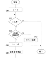
図11は制御部18が第2のプログラムのロードが可能かどうかを判定する処理を示す。ここでNは第2のプログラムの設定に必要な行数である。まず、カウンタiを「1」とし(S30)、iとNを比較する(S32)。iがN以下であれば設定は完了していないため、S34へ進み、i行目の空いているALUに第2のプログラムの実現に必要な命令をすべて収容できるか否かを判定する。これは、ALUの空き数をもとに判断される。収容可能であれば(S34のY)設定データ17に反映してiをインクリメントし(S36)、その行で新たに設定したALUの個数だけ空き数を減らし(S38)、S32へ戻る。
【0039】
S34において、i行目への命令の収容が不可能だったとき、すなわち、収容すべき命令の数が空き数を上回ったとき(S34のN)、エラー処理(S40)を実行して処理を終える。エラー処理(S40)として、このアレイ以外のアレイへの第2のプログラムのロードがある。別の処理として、後述の図14の処理がある。一方、S32において、iの値がすでにNを超えていれば、全命令の設定が完了したことになるので、同じく処理を終える。
【0040】
図12、図13は、第2のプログラムが設定された状態を各命令とALUの座標表示の関係で示している。subは(1,3)のごとく、空いていたALUを利用している。図13は、第1、第2のプログラムを実装した状態のアレイの様子を示す。
【0041】
図14は、前述のエラー処理の一例を示す。最初に処理の概要を述べ、後に実例を挙げる。
図14のごとく、まずカウンタi、j、kに「1」をセットする(S50)。ここでkは、新たにロードすべきプログラムを構成する第k番目の命令とし、そのプログラムには全部L個の命令があるとする。
【0042】
制御部18は、kがL以下(S52)で、iがZ以下(S54)で、jがW以下(S56)のとき、(i,j)のALUが空いているかどうか調べる(S58)。空いていれば第kの命令がそのALUに設定可能かどうか検査する(S60)。後述のごとく、ALUが空いていても、この命令に必要な入力ノード数と出力ノード数によっては、このALUが使用できないことがある。検査の結果使用できるとわかれば(S60のY)、設定データ17に反映し、kをインクリメントし(S62)、jをインクリメントし(S64)、S52へ戻る。S60でALUが第k命令のために使用できないとわかれば(S60のN)、S62をスキップしてS64へ進む。S58で(i,j)が空いていないことがわかれば、S60とS62をスキップしてS64へ進む。
【0043】
S56でjがすでにWを超えていれば、その行の検査は終わっているため(S56のN)、次の行を検査すべくjを「1」に戻し、iをインクリメントし(S66)、S54へ戻る。
【0044】
S54でiがすでにZを超えていれば、このプログラムの設定が完了せずに終わったため、エラー処理(S68)を実行して処理を終える。一方、S52でkがすでにLを超えていれば、このプログラムの設定が完了したため、正常に処理を終える。S68のエラー処理として、このプログラムを別のアレイへロードする等がある。以上が処理の大筋である。
【0045】
図15以下、図11および図14の処理を総括して実例で示す。ここでは、複数のプログラムに対応する第1データフローグラフ、第2データフローグラフ、・・・を設定する場合、アレイの空き領域に合わせて適宜データフローグラフを変形することにある。データフローグラフの設定は以下の手順に従う。
【0046】
(1) 第1データフローグラフを設定する。
(2) 第1データフローグラフの設定情報から未設定のALUに関する情報を取得し、その未設定のALUに第2データフローグラフが設定できれば、そのまま設定する(図11の場合)。
(3) 未設定のALUに第2データフローグラフが収まらない場合、第2データフローグラフを変形し、設定する(図14の場合)。
(4) どのように変形しても第2データフローグラフが収まらない場合、残りのデータフローグラフに対して設定処理を行う(図14のエラー処理)。
(5) 最終的に設定できなかったデータフローグラフは、別のALUアレイに設定を行う(同エラー処理)。
【0047】
図15、図16、図17は、設定すべき3つのデータフローグラフを模式的に示す。但し、番号はノードの番号を表し、各ノードには所定の論理演算が割り当てられている。また、アレイは8×8とする。
【0048】
まず、アレイは初期状態では未設定の状態なので、第1データフローグラフはそのまま設定できる。図18はその状態を示す。図19はこの時点でのALUの空き状態を示す。
【0049】
つぎに、第2データフローグラフを設定する。図19の空き状態と図16の必要なALU数から、第2データフローグラフもそのまま設定できることが分かる。図20は、アレイに第2データフローグラフを設定しおえた状態を示す。また、図21はこの時点でのALUの空き状態を示す。
【0050】
最後に、第3データフローグラフを設定する。図17から判明する必要なALU数と図19から判明する空き状態を比較すると、第3データフローグラフはそのままの接続状態ではアレイに設定できないことがわかる。第3データフローグラフの接続状態を変更することにより、設定が可能になるか検査する。アレイにノードを設定する規則は以下の通りである。
【0051】
(1) できるだけ上の行(iが小さい行)に設定する。
(2) できるだけ左寄りの列(jが小さい列)に設定する。
(3) 空いているALUが不足するなどの問題があり、データフローグラフを変形するとき、適宜スルーノードを追加する。
【0052】
図19に示す未使用のALUの位置を分かりやすくするため、既述の座標表示を使う。最上行から検査すると、(8,1)に設定できるのは、入力ノード数0で出力ノード数1のノードのみである。図22は第3データフローグラフを構成する各ノードの入力ノード数と出力ノード数を示す。図22から、ノード24を(8,1)に設定する。図23はこの時点での設定状態を上3行について示す。
【0053】
次に、設定したノード24の出力ノードを調べる。ノード24は出力ノードとしてノード28を持つが、ノード28は入力ノード数2であるため、(8,2)には設定できない。従って、更に下行に設定する。ここでは左寄せにするので、ノード28を仮に(6,3)に設定する。しかし、その場合でもノード28の2つの入力ノードの設定できないため、更に下行であって左寄せを満たす(4,4)に設定する。ノード24とノード28は接続されているので、(6,3)、(8,2)にスルーノード(図中「N」)を設定することにより接続する。図24はこの時点での設定状態を示す。
【0054】
つづいて、ノード28の入力ノードであるノード25を設定する。ノード25はノード28の上行に設定すればよいので、(7,3)へ設定する。以上でノード28の入力ノードの設定が終了する。図25はこの時点での設定状態を示す。
【0055】
次に、ノード28の出力ノードはノード31のみである。既述同様、ノード31を設定し、ノード31の入力ノードのうち未設定のノード29を(5,4)に設定する。更にノード29の入力ノードのうち未設定のノード26を(8,4)に設定する。図26はこの時点での設定状態を示す。
【0056】
つづいて、ノード31の出力のノード33を設定する。ノード33は入力ノード数が2であるので(1,6)に設定を行い、その入力ノードの設定を前述同様に設定する。しかし、ノード30の入力ノードのノード27に対して設定可能なALUがないため、設定は失敗となる。よって、ノード33以降の設定をクリアする。図27はクリア前の設定状態を示す。
【0057】
ノード27を設定するために(1,6)にスルーノードを挿入し、ノード33の設定位置を1行下げてスペースを作る。ノード33は(1,7)へ設定する。以上の手順で、図28のごとく、第3データフローグラフの設定が完了する。
【0058】
以上、本発明を実施の形態をもとに説明した。実施の形態は例示であり、それらの各構成要素や各処理プロセスの組み合わせにいろいろな変形例が可能なこと、またそうした変形例も本発明の範囲にあることは当業者に理解されるところである。以下、そうした例を挙げる。
【0059】
図1のデータ設定装置24その他にタイマー(図示せず)を設け、制御部18がタイマー出力に応じてリコンフィギュラブル回路12にロードする機能を切り替えてもよい。その場合、複数の機能を順次切り替えて実現することができる。この方法は、集積回路装置10にいろいろな機能を時分割で行わせる場合、有効である。
【0060】
実施の形態の集積回路装置10は、例えばソフトウエア無線機に応用できる。その場合、リコンフィギュラブル回路12には、適宜FMラジオ、カーナビゲーション機能、テレビジョン受像機能、音声通話機能などをロードすればよい。
【0061】
【発明の効果】
本発明のデータ設定装置によれば、集積回路装置の利用効率を改善することができる。また、同じ機能を実現する際、回路規模、消費電力を削減することができる。
【図面の簡単な説明】
【図1】 実施の形態に係る集積回路装置およびデータ設定装置の構成図である。
【図2】 図1のリコンフィギュラブル回路の中のALUアレイ部分の構成図である。
【図3】 あるプログラムの処理を表したデータフローグラフを示す図である。
【図4】 図3のデータフローグラフに対応してマッピングされたALUアレイの構成図である。
【図5】 2×4のALUアレイを座標表示して示す図である。
【図6】 命令セットとALUの対応関係を示す図である。
【図7】 命令セットとALUの対応関係を示す図である。
【図8】 監視部がALUの空き状態を検査する手順を示すフローチャートである。
【図9】 ALUアレイにロードすべき第2のプログラムのデータフローグラフを示す図である。
【図10】 第1のプログラムを考慮しない場合、第2のプログラムの命令セットとALUの対応関係を示す図である。
【図11】 第2のプログラムが、あるALUアレイにロード可能かどうかを判定する手順を示すフローチャートである。
【図12】 第1のプログラムを考慮した場合、第2のプログラムの命令セットとALUの対応関係を示す図である。
【図13】 第1および第2のプログラムがALUアレイにロードされた状態を示す図である。
【図14】 第2以下のプログラムをALUアレイにロードする際、ロード可能か否かを判定する手順を示し、とくに図11のエラー処理の一例を示すフローチャートである。
【図15】 第1データフローグラフで使用すべきALUを番号をつけて示す図である。
【図16】 第2データフローグラフで使用すべきALUを番号をつけて示す図である。
【図17】 第3データフローグラフで使用すべきALUを番号をつけて示す図である。
【図18】 第1データフローグラフを8×8のALUアレイにロードした状態を示す図である。
【図19】 図18の時点でのALUの使用状態を示す図である。
【図20】 第2データフローグラフを8×8のALUアレイにロードした状態を示す図である。
【図21】 図20の時点でのALUの使用状態を示す図である。
【図22】 第3データフローグラフに必要なALUの入力および出力ノード数を示す図である。
【図23】 第3データフローグラフのノード「24」を設定した状態を示す図である。
【図24】 第3データフローグラフのノード「28」を設定した状態を示す図である。
【図25】 第3データフローグラフのノード「25」を設定した状態を示す図である。
【図26】 第3データフローグラフのノード「26」「29」「31」を設定した状態を示す図である。
【図27】 第3データフローグラフのノード「27」が設定できず、設定が一時的に失敗して状態を示す図である。
【図28】 図28の失敗を解消して第3データフローグラフの設定が完了した状態を示す図である。
【符号の説明】
10 集積回路装置、 12 リコンフィギュラブル回路、 12a ALUアレイ、 14 設定部、 18 制御部、 20 コンパイル部、 21 データフローグラフ、 23 監視部、 24 データ設定装置。[0001]
BACKGROUND OF THE INVENTION
The present invention relates to a data generation device that generates setting data for loading an intended function to an integrated circuit such as a reconfigurable circuit .
[0002]
[Prior art]
Recently, wireless communications such as mobile phones, GPS, and VICS have become widespread, and the types of wireless devices are increasing. If these radios or their functions are all implemented by hardware, the cost and mounting area increase. Therefore, there is a concept of “software radio” that implements various functions by installing a circuit having general-purpose capability as hardware and switching software loaded thereon.
[0003]
Circuits that implement a software defined radio include an FPGA (Field Programmable Gate Array) and a DSP (Digital Signal Processor).
[0004]
[Patent Document 1]
JP-A-10-256383 (full text, Fig. 1-4)
[0005]
[Problems to be solved by the invention]
Based on the FPGA, various logics can be realized by using a look-up table (LUT) for storing the truth table of the logic circuit, but in general, the unit of the logic element is small, and the desired function is realized. In addition, many LUTs and wiring resources are required. As a result, compared with a normal LSI, the mounting area is generally large and the cost is high. In addition, the program time for rewriting a circuit is long to some extent, and is often not suitable for real-time function switching.
[0006]
The present invention has been made in view of such a current situation, and an object of the present invention is to provide a reconfigurable circuit that is advantageous in terms of cost, rewriting speed, circuit utilization efficiency, power consumption, and the like, an integrated circuit device using the same, and data setting To provide an apparatus.
[0007]
[Means for Solving the Problems]
An aspect of the present invention relates to a data generation apparatus that generates setting data for loading an intended function into an array of logic circuits each capable of selectively performing a plurality of arithmetic logic functions, and is used in the array. A monitoring unit that monitors a region that is present, a storage unit that stores setting data based on a data flow graph for setting a function of each logic circuit in the array and a connection relationship between the logic circuits, and the setting from the storage unit A control unit that reads data and generates setting data for loading a function to an unused area in the array based on the information on the used area obtained by monitoring by the monitoring unit, and generated by the control unit A setting unit that loads the set data to the array, and the control unit includes a functional circuit related to the setting data read from the storage unit. Whether the data can be loaded into the array is determined from the use status of the array as the monitoring result. If the functional circuit cannot be loaded, the setting data is changed so that the functional circuit can be loaded into the array. .
[0008]
For example, the setting unit may be constituted by dedicated hardware in addition to a combination of CPU (central processing unit) programs included in the device. The array is configured by arranging 8 × 8 logic circuits, for example. As a result of loading a plurality of functions into an array, ie, the smallest unit of a functional configuration, the effective utilization rate of the array is increased.
[0009]
The control unit receives the result of monitoring by the monitoring unit, and generates setting data for loading another function in an unused area in the array, thereby increasing the utilization efficiency of the array.
[0010]
Note that the control unit and the monitoring unit include, for example, a combination of a compiler, a CPU, and other arbitrary hardware and software.
[0011]
In the above configuration, the control unit may change the setting data by appropriately inserting a through node into the setting data.
[0012]
“ Through node” means NOP (no operation), that is, a node that does nothing. Actually, a wiring simply connecting an input and an output is selected inside the logic circuit, or the logic circuit is an identity mapping operator, ie, multiplication. If a circuit that multiplies 1 as an adder or adds zero as an adder is set, this logic circuit becomes a through node.
[0013]
The data generation device may be an external device that provides setting data to the integrated circuit device including the above-described logic circuit array , for example, and a program written in the C language or other high-level language is used as the setting data. A compiler for conversion may be provided.
[0014]
The monitoring unit may monitor an area used in the logic circuit array at a timing such as when data is sent from the control unit to the setting unit or when data is set by the setting unit. .
[0015]
The integrated circuit device and the data setting device described above may be a single device. In this case, for example, the former setting unit and the latter control unit can be configured by a single CPU and program. Part of the former and part of the latter may be configured as a single device.
[0016]
In any of the above cases, the logic circuit array is an array in which a plurality of rows of logic circuits arranged in the horizontal direction are combined in the vertical direction, and there is no connection for connection between the logic circuits in the horizontal direction. A structure in which a connection for connection is provided between the output of the first logic circuit row and the input of the next-stage logic circuit row may be employed.
[0017]
It should be noted that any combination of the above components and the expression of the present invention expressed as a method, apparatus, system, and computer program are also effective as an aspect of the present invention.
[0018]
DETAILED DESCRIPTION OF THE INVENTION
The embodiment relates to a reconfigurable circuit having an ALU (Arithmetic Logic Unit) array as a basic element. In this type of circuit, one ALU constitutes one logical unit, and this logical unit can selectively execute a plurality of arithmetic operations. Therefore, the circuit configuration is simple, and a data flow graph described later is directly used. Since mapping is possible, configuration time can be saved. Mapping refers to an instruction set of a program to be executed by the reconfigurable circuit and a connection data set required in the reconfigurable circuit to realize the instruction set loaded into an ALU array (hereinafter also simply referred to as “array”). To set. The configuration is defined below.
[0019]
1. Array: ALU is arranged in a matrix of m × n.
2. Reconfigurable circuit: A plurality of arrays are built in, but in the following description, attention is paid to one array (hereinafter, this array is also referred to as “target array”).
[0020]
An ALU is a “logical unit”, but normally one ALU realizes one function. For this reason, the array becomes a “functional unit”. The setting of the size of the array, that is, the values of m and n described above, is made from an empirical rule based on the assumption of the function to be realized. If the array is too small, one function cannot be realized. On the other hand, if the array is too large, when one function is loaded, unused ALUs increase and use efficiency is poor.
[0021]
From this point of view, the feature of the embodiment is that a plurality of functions are mounted in an array which is a functional unit. That is, first, the first functional circuit is loaded, and if there is an unused area, the second functional circuit is loaded to effectively use the array. Of course, it is effective to load the third and lower functional circuits in the remaining area.
[0022]
FIG. 1 shows a configuration of an
[0023]
The
[0024]
The
The
[0025]
The
[0026]
The
[0027]
The setting
[0028]
FIG. 2 shows the configuration of the
[0029]
As shown in the figure, Y ALUs are arranged in the horizontal direction and X ALUs are arranged in the vertical direction, and input variables and constants are input to ALU11, ALU12,..., ALU1Y in the first row. Depending on the setting, a predetermined calculation is performed. The output of the calculation result is input to the
[0030]
The setting
[0031]
Consider the following execution target program.
[0032]
Hereinafter, a method for loading two or more functional circuits will be described. Now, as shown in FIG. 5, the coordinates of the ALU included in the 2 × 4 array are represented by (i, j). However, i = 1, 2, j = 1, 2, 3, 4. 6 and 7 show the settings of FIG. 4 in coordinates. Here, for example, two mul and one add are respectively set to (1, 1) (1, 2) (2, 1), and the outputs of (1, 1) and (1, 2) are both (2, 1) connected to the input.
[0033]
The
[0034]
In S16, it is checked whether the ALU of (i, j) is not set, that is, it is free. If it is free (Y in S16), “the number of vacant i rows is W−j + 1 and the number of used is j−1”. (S22), i is incremented and j is returned to "1" (S24), and the process returns to S12 to investigate the next line. If the (i, j) ALU has been used in S16, the process proceeds to S18, j is incremented, and the process returns to S14.
[0035]
If j has already exceeded the value of W in S14 (N in S14), since there is no vacancy in the row, “the number of vacant i rows is zero and the number of uses is W” is output (S20), S24 Proceed to
[0036]
If i has already exceeded Z in S12 (N in S12), the process is terminated because all rows have been investigated. Through the above processing, the
[0037]
A second program, that is, a second functional circuit is set in this array. The program is as follows.
[0038]
FIG. 11 shows a process in which the
[0039]
In S34, when the instruction cannot be accommodated in the i-th line, that is, when the number of instructions to be accommodated exceeds the number of vacant (N in S34), error processing (S40) is executed to perform the process. Finish. Error processing (S40) includes loading of the second program to an array other than this array. As another process, there is a process shown in FIG. On the other hand, if the value of i has already exceeded N in S32, the setting of all instructions has been completed, and thus the processing is also finished.
[0040]
FIG. 12 and FIG. 13 show the state in which the second program is set in relation to each instruction and ALU coordinate display. Sub uses a free ALU as in (1, 3). FIG. 13 shows a state of the array in which the first and second programs are mounted.
[0041]
FIG. 14 shows an example of the error processing described above. First, an outline of the processing is described, and an example is given later.
As shown in FIG. 14, first, "1" is set in the counters i, j, and k (S50). Here, k is assumed to be the k-th instruction constituting a program to be newly loaded, and all the programs have L instructions.
[0042]
When k is L or less (S52), i is Z or less (S54), and j is W or less (S56), the
[0043]
If j has already exceeded W in S56, the inspection of that line has been completed (N in S56), so j is returned to "1" to inspect the next line, i is incremented (S66), Return to S54.
[0044]
If i has already exceeded Z in S54, the setting of this program has been completed without completion, and error processing (S68) is executed to finish the processing. On the other hand, if k has already exceeded L in S52, since the setting of this program is completed, the processing is normally completed. As an error process of S68, there is a load of this program to another array. The above is the outline of the processing.
[0045]
FIG. 15 and subsequent figures collectively show the processes of FIGS. 11 and 14 by way of examples. Here, when setting the first data flow graph, the second data flow graph,... Corresponding to a plurality of programs, the data flow graph is appropriately modified in accordance with the free area of the array. Follow the procedure below to set up the data flow graph.
[0046]
(1) Set the first data flow graph.
(2) Information related to the unset ALU is acquired from the setting information of the first data flow graph, and if the second data flow graph can be set in the unset ALU, it is set as it is (in the case of FIG. 11).
(3) If the second data flow graph does not fit in the unset ALU, the second data flow graph is transformed and set (in the case of FIG. 14).
(4) If the second data flow graph does not fit no matter how it is transformed, setting processing is performed on the remaining data flow graph (error processing in FIG. 14).
(5) The data flow graph that could not be finally set is set in another ALU array (same error processing).
[0047]
FIGS. 15, 16, and 17 schematically show three data flow graphs to be set. However, the number represents a node number, and a predetermined logical operation is assigned to each node. The array is 8 × 8.
[0048]
First, since the array is in an unset state in the initial state, the first data flow graph can be set as it is. FIG. 18 shows this state. FIG. 19 shows the free state of the ALU at this point.
[0049]
Next, a second data flow graph is set. It can be seen that the second data flow graph can be set as it is based on the empty state in FIG. 19 and the necessary number of ALUs in FIG. FIG. 20 shows a state in which the second data flow graph has been set in the array. FIG. 21 shows the free state of the ALU at this time.
[0050]
Finally, a third data flow graph is set. Comparing the necessary number of ALUs found from FIG. 17 and the free state found from FIG. 19, it can be seen that the third data flow graph cannot be set in the array in the same connection state. It is checked whether setting is possible by changing the connection state of the third data flow graph. The rules for setting nodes in the array are as follows.
[0051]
(1) Set the line as high as possible (the line where i is small).
(2) Set the column to the left as much as possible (a column where j is small).
(3) There is a problem such as a shortage of free ALUs, and when transforming the data flow graph, through nodes are added as appropriate.
[0052]
In order to make the positions of unused ALUs shown in FIG. 19 easier to understand, the above-described coordinate display is used. Inspecting from the top row, only nodes with 0 input nodes and 1 output nodes can be set to (8, 1). FIG. 22 shows the number of input nodes and the number of output nodes of each node constituting the third data flow graph. From FIG. 22, the
[0053]
Next, the output node of the
[0054]
Subsequently, the
[0055]
Next,
[0056]
Subsequently, an
[0057]
In order to set the
[0058]
The present invention has been described based on the embodiments. The embodiments are exemplifications, and it will be understood by those skilled in the art that various modifications can be made to combinations of the respective constituent elements and processing processes, and such modifications are within the scope of the present invention. . Here are some examples.
[0059]
A timer (not shown) may be provided in the
[0060]
The
[0061]
【The invention's effect】
According to the data setting device of the present invention, the utilization efficiency of the integrated circuit device can be improved. Further, when realizing the same function, the circuit scale and power consumption can be reduced.
[Brief description of the drawings]
FIG. 1 is a configuration diagram of an integrated circuit device and a data setting device according to an embodiment.
FIG. 2 is a configuration diagram of an ALU array portion in the reconfigurable circuit of FIG. 1;
FIG. 3 is a diagram showing a data flow graph representing processing of a certain program.
4 is a configuration diagram of an ALU array mapped corresponding to the data flow graph of FIG. 3. FIG.
FIG. 5 is a diagram showing coordinates of a 2 × 4 ALU array.
FIG. 6 is a diagram illustrating a correspondence relationship between an instruction set and an ALU.
FIG. 7 is a diagram illustrating a correspondence relationship between an instruction set and an ALU.
FIG. 8 is a flowchart illustrating a procedure for a monitoring unit to check the availability of an ALU.
FIG. 9 is a diagram showing a data flow graph of a second program to be loaded into the ALU array.
FIG. 10 is a diagram illustrating a correspondence relationship between an instruction set of a second program and an ALU when the first program is not considered.
FIG. 11 is a flowchart showing a procedure for determining whether or not a second program can be loaded into a certain ALU array;
FIG. 12 is a diagram illustrating a correspondence relationship between the instruction set of the second program and the ALU when the first program is considered.
FIG. 13 is a diagram showing a state in which the first and second programs are loaded into the ALU array.
FIG. 14 is a flowchart showing a procedure for determining whether or not the second and subsequent programs are loaded into the ALU array, and particularly showing an example of error processing in FIG.
FIG. 15 is a diagram showing ALUs to be used in the first data flow graph with numbers.
FIG. 16 is a diagram showing ALUs to be used in the second data flow graph with numbers.
FIG. 17 is a diagram showing numbers of ALUs to be used in the third data flow graph.
FIG. 18 is a diagram illustrating a state in which a first data flow graph is loaded into an 8 × 8 ALU array.
FIG. 19 is a diagram showing a usage state of the ALU at the time of FIG.
FIG. 20 is a diagram showing a state in which a second data flow graph is loaded into an 8 × 8 ALU array.
FIG. 21 is a diagram showing a usage state of the ALU at the time of FIG.
FIG. 22 is a diagram showing the number of ALU input and output nodes required for the third data flow graph.
FIG. 23 is a diagram showing a state in which a node “24” of the third data flow graph is set.
FIG. 24 is a diagram showing a state where a node “28” of the third data flow graph is set.
FIG. 25 is a diagram showing a state in which a node “25” of the third data flow graph is set.
FIG. 26 is a diagram illustrating a state where nodes “26”, “29”, and “31” of the third data flow graph are set.
FIG. 27 is a diagram illustrating a state in which the node “27” of the third data flow graph cannot be set and the setting temporarily fails.
FIG. 28 is a diagram illustrating a state in which the failure of FIG. 28 is resolved and the setting of the third data flow graph is completed.
[Explanation of symbols]
DESCRIPTION OF
Claims (3)
前記アレイにおいて使用されている領域を監視する監視部と、
前記設定データを構成するためのデータフローグラフを記憶する記憶部と、
前記記憶部から前記データフローグラフを読み込み、前記監視部による監視により得られた前記使用領域の情報に基づいて、前記アレイにおいて未使用の領域に機能をロードするための設定データを生成する制御部と、
前記制御部で生成された設定データを前記アレイにロードする設定部と、を備え、
前記制御部は、
前記記憶部から読み込んだデータフローグラフに基づいて構成される機能回路が前記アレイにロードできるかどうかを、前記監視部での監視により得られた前記アレイの使用状況から判断し、
前記機能回路のロードができない場合、前記記憶部から読み込んだデータフローグラフの変形を行うデータ生成装置。 A data generation device for generating setting data for loading a functional circuit into an array of logic circuits,
A monitoring unit for monitoring an area used in the array;
A storage unit for storing a data flow graph for configuring the setting data ;
A control unit that reads the data flow graph from the storage unit and generates setting data for loading a function into an unused region in the array based on the information on the used region obtained by monitoring by the monitoring unit When,
A setting unit that loads setting data generated by the control unit into the array;
The controller is
Whether the functional circuit configured based on the data flow graph read from the storage unit can be loaded into the array is determined from the usage status of the array obtained by monitoring in the monitoring unit,
A data generation device that performs transformation of the data flow graph read from the storage unit when the functional circuit cannot be loaded.
Priority Applications (1)
| Application Number | Priority Date | Filing Date | Title |
|---|---|---|---|
| JP2003095039A JP3989397B2 (en) | 2003-03-31 | 2003-03-31 | Integrated circuit device and data setting device for the device |
Applications Claiming Priority (1)
| Application Number | Priority Date | Filing Date | Title |
|---|---|---|---|
| JP2003095039A JP3989397B2 (en) | 2003-03-31 | 2003-03-31 | Integrated circuit device and data setting device for the device |
Publications (2)
| Publication Number | Publication Date |
|---|---|
| JP2004302856A JP2004302856A (en) | 2004-10-28 |
| JP3989397B2 true JP3989397B2 (en) | 2007-10-10 |
Family
ID=33407459
Family Applications (1)
| Application Number | Title | Priority Date | Filing Date |
|---|---|---|---|
| JP2003095039A Expired - Fee Related JP3989397B2 (en) | 2003-03-31 | 2003-03-31 | Integrated circuit device and data setting device for the device |
Country Status (1)
| Country | Link |
|---|---|
| JP (1) | JP3989397B2 (en) |
Families Citing this family (2)
| Publication number | Priority date | Publication date | Assignee | Title |
|---|---|---|---|---|
| JP4597075B2 (en) * | 2006-03-09 | 2010-12-15 | 三洋電機株式会社 | Operation mapping method to reconfigurable circuit, reconfigurable circuit, and data flow graph |
| JP5355152B2 (en) * | 2009-03-10 | 2013-11-27 | 三菱電機株式会社 | Dynamic reconfiguration device |
-
2003
- 2003-03-31 JP JP2003095039A patent/JP3989397B2/en not_active Expired - Fee Related
Also Published As
| Publication number | Publication date |
|---|---|
| JP2004302856A (en) | 2004-10-28 |
Similar Documents
| Publication | Publication Date | Title |
|---|---|---|
| JP4104538B2 (en) | Reconfigurable circuit, processing device provided with reconfigurable circuit, function determination method of logic circuit in reconfigurable circuit, circuit generation method, and circuit | |
| US7120903B2 (en) | Data processing apparatus and method for generating the data of an object program for a parallel operation apparatus | |
| US20050283768A1 (en) | Data flow graph processing method, reconfigurable circuit and processing apparatus | |
| US20050283743A1 (en) | Method for generating hardware information | |
| US11171652B2 (en) | Method and apparatus for implementing configurable streaming networks | |
| WO2018067251A1 (en) | Methods and apparatus for dynamically configuring soft processors on an integrated circuit | |
| Marconi | Online scheduling and placement of hardware tasks with multiple variants on dynamically reconfigurable field-programmable gate arrays | |
| US7716458B2 (en) | Reconfigurable integrated circuit, system development method and data processing method | |
| US20080122482A1 (en) | Data Processing System | |
| JP5007838B2 (en) | Information processing apparatus and information processing program | |
| JP3989397B2 (en) | Integrated circuit device and data setting device for the device | |
| JP6485335B2 (en) | Arithmetic processing device and control method of arithmetic processing device | |
| JP3850531B2 (en) | Reconfigurable circuit design device and reconfigurable circuit device | |
| Fricke et al. | Automatic tool-flow for mapping applications to an application-specific cgra architecture | |
| JP2006018411A (en) | Processor | |
| JPH11232077A (en) | Information processing system | |
| JP2018206195A (en) | Calculation system, and control method and program of calculation system | |
| US7017033B2 (en) | Arithmetic apparatus and arithmetic method | |
| JP4208919B2 (en) | Activation code generation method | |
| US20240020449A1 (en) | Fast CAD Compilation Through Coarse Macro Lowering | |
| Masselos et al. | Introduction to reconfigurable hardware | |
| JP4562679B2 (en) | Data flow graph generator | |
| Möller et al. | FiPRe: An implementation model to enable self-reconfigurable applications | |
| JP6553694B2 (en) | Processor element, programmable device and control method of processor element | |
| Nestor | L3: An FPGA-based multilayer maze routing accelerator |
Legal Events
| Date | Code | Title | Description |
|---|---|---|---|
| A621 | Written request for application examination |
Free format text: JAPANESE INTERMEDIATE CODE: A621 Effective date: 20050512 |
|
| A977 | Report on retrieval |
Free format text: JAPANESE INTERMEDIATE CODE: A971007 Effective date: 20061130 |
|
| A131 | Notification of reasons for refusal |
Free format text: JAPANESE INTERMEDIATE CODE: A131 Effective date: 20061205 |
|
| A521 | Written amendment |
Free format text: JAPANESE INTERMEDIATE CODE: A523 Effective date: 20070201 |
|
| TRDD | Decision of grant or rejection written | ||
| A01 | Written decision to grant a patent or to grant a registration (utility model) |
Free format text: JAPANESE INTERMEDIATE CODE: A01 Effective date: 20070619 |
|
| A61 | First payment of annual fees (during grant procedure) |
Free format text: JAPANESE INTERMEDIATE CODE: A61 Effective date: 20070717 |
|
| FPAY | Renewal fee payment (event date is renewal date of database) |
Free format text: PAYMENT UNTIL: 20100727 Year of fee payment: 3 |
|
| FPAY | Renewal fee payment (event date is renewal date of database) |
Free format text: PAYMENT UNTIL: 20100727 Year of fee payment: 3 |
|
| FPAY | Renewal fee payment (event date is renewal date of database) |
Free format text: PAYMENT UNTIL: 20110727 Year of fee payment: 4 |
|
| FPAY | Renewal fee payment (event date is renewal date of database) |
Free format text: PAYMENT UNTIL: 20120727 Year of fee payment: 5 |
|
| FPAY | Renewal fee payment (event date is renewal date of database) |
Free format text: PAYMENT UNTIL: 20130727 Year of fee payment: 6 |
|
| LAPS | Cancellation because of no payment of annual fees |