JP2009247121A - Power conversion apparatus - Google Patents
Power conversion apparatus Download PDFInfo
- Publication number
- JP2009247121A JP2009247121A JP2008091029A JP2008091029A JP2009247121A JP 2009247121 A JP2009247121 A JP 2009247121A JP 2008091029 A JP2008091029 A JP 2008091029A JP 2008091029 A JP2008091029 A JP 2008091029A JP 2009247121 A JP2009247121 A JP 2009247121A
- Authority
- JP
- Japan
- Prior art keywords
- coil
- winding
- switch element
- inductor
- power converter
- Prior art date
- Legal status (The legal status is an assumption and is not a legal conclusion. Google has not performed a legal analysis and makes no representation as to the accuracy of the status listed.)
- Pending
Links
Images


Classifications
-
- H—ELECTRICITY
- H02—GENERATION; CONVERSION OR DISTRIBUTION OF ELECTRIC POWER
- H02M—APPARATUS FOR CONVERSION BETWEEN AC AND AC, BETWEEN AC AND DC, OR BETWEEN DC AND DC, AND FOR USE WITH MAINS OR SIMILAR POWER SUPPLY SYSTEMS; CONVERSION OF DC OR AC INPUT POWER INTO SURGE OUTPUT POWER; CONTROL OR REGULATION THEREOF
- H02M1/00—Details of apparatus for conversion
- H02M1/42—Circuits or arrangements for compensating for or adjusting power factor in converters or inverters
- H02M1/4208—Arrangements for improving power factor of AC input
- H02M1/4225—Arrangements for improving power factor of AC input using a non-isolated boost converter
-
- H—ELECTRICITY
- H02—GENERATION; CONVERSION OR DISTRIBUTION OF ELECTRIC POWER
- H02M—APPARATUS FOR CONVERSION BETWEEN AC AND AC, BETWEEN AC AND DC, OR BETWEEN DC AND DC, AND FOR USE WITH MAINS OR SIMILAR POWER SUPPLY SYSTEMS; CONVERSION OF DC OR AC INPUT POWER INTO SURGE OUTPUT POWER; CONTROL OR REGULATION THEREOF
- H02M1/00—Details of apparatus for conversion
- H02M1/12—Arrangements for reducing harmonics from ac input or output
- H02M1/123—Suppression of common mode voltage or current
-
- Y—GENERAL TAGGING OF NEW TECHNOLOGICAL DEVELOPMENTS; GENERAL TAGGING OF CROSS-SECTIONAL TECHNOLOGIES SPANNING OVER SEVERAL SECTIONS OF THE IPC; TECHNICAL SUBJECTS COVERED BY FORMER USPC CROSS-REFERENCE ART COLLECTIONS [XRACs] AND DIGESTS
- Y02—TECHNOLOGIES OR APPLICATIONS FOR MITIGATION OR ADAPTATION AGAINST CLIMATE CHANGE
- Y02B—CLIMATE CHANGE MITIGATION TECHNOLOGIES RELATED TO BUILDINGS, e.g. HOUSING, HOUSE APPLIANCES OR RELATED END-USER APPLICATIONS
- Y02B70/00—Technologies for an efficient end-user side electric power management and consumption
- Y02B70/10—Technologies improving the efficiency by using switched-mode power supplies [SMPS], i.e. efficient power electronics conversion e.g. power factor correction or reduction of losses in power supplies or efficient standby modes
-
- Y—GENERAL TAGGING OF NEW TECHNOLOGICAL DEVELOPMENTS; GENERAL TAGGING OF CROSS-SECTIONAL TECHNOLOGIES SPANNING OVER SEVERAL SECTIONS OF THE IPC; TECHNICAL SUBJECTS COVERED BY FORMER USPC CROSS-REFERENCE ART COLLECTIONS [XRACs] AND DIGESTS
- Y02—TECHNOLOGIES OR APPLICATIONS FOR MITIGATION OR ADAPTATION AGAINST CLIMATE CHANGE
- Y02P—CLIMATE CHANGE MITIGATION TECHNOLOGIES IN THE PRODUCTION OR PROCESSING OF GOODS
- Y02P80/00—Climate change mitigation technologies for sector-wide applications
- Y02P80/10—Efficient use of energy, e.g. using compressed air or pressurized fluid as energy carrier
Abstract
Description
本発明は、交流電圧からスイッチング素子をオンオフ制御して、コイルに蓄積されたエネルギーを直流電圧として出力する電力変換装置に関し、とくに昇圧、あるいは降圧チョッパとして動作する電力変換装置に関する。 The present invention relates to a power conversion device that controls on / off of a switching element from an AC voltage and outputs energy stored in a coil as a DC voltage, and more particularly to a power conversion device that operates as a step-up or step-down chopper.
従来のスイッチ素子を利用した電力変換装置としては、たとえば図5に示すような力率改善回路を整流回路の出力側に設けたものがある。図5の電力変換装置において、交流電源1は、スイッチング電源装置10を介して負荷20に直流電圧を供給する。
As a conventional power conversion device using a switch element, for example, there is one in which a power factor correction circuit as shown in FIG. 5 is provided on the output side of a rectifier circuit. In the power conversion apparatus of FIG. 5, the
スイッチング電源装置10は、コンデンサ2a〜2cとコモンモードチョークコイル3からなるノイズフィルタ2、ダイオード4a〜4dからなる整流回路4、この整流回路4の出力ライン側に配置された力率改善用のインダクタ5、PWM制御回路6aによってオンオフ制御されるスイッチ素子6、およびダイオード7とコンデンサ8からなる平滑回路によって構成されている。ここで、ノイズフィルタ2は交流電源1からの伝導ノイズ(コモンモードノイズ)を低減するために配置されている。また、スイッチ素子6には自己消弧形デバイスとしてMOSFETを使用している。
The
つぎに、電力変換装置10の動作を説明する。
最初に、スイッチ素子6がオンのときインダクタ5に電流が流れて、そこにエネルギーが蓄積される。つぎに、スイッチ素子6がオフになると、インダクタ5に発生する逆起電力によって蓄積されたエネルギーが負荷20に伝達される。このとき、入力電流波形が正弦波状になるように、制御回路8によりスイッチ素子6のオンオフのパルス幅を制御して、力率を改善する。
Next, the operation of the
First, when the switch element 6 is on, a current flows through the
こうしたPWMインバータなどの電力変換装置を構成する順変換回路や逆変換回路に用いられるMOSFETなどのスイッチング動作は、キャリア周波数を数KHzから十数KHz程度としたパルス幅変調(PWM)された駆動信号に基づいて行われ、このスイッチング動作により数十KHz以上の周波数成分のコモンモードノイズがこの電力変換装置の主回路導体と接地(アース)との間に発生することが知られている。 Switching operations such as MOSFETs used in forward conversion circuits and reverse conversion circuits constituting such power converters as PWM inverters are pulse width modulated (PWM) drive signals in which the carrier frequency is about several KHz to several tens of KHz. It is known that common mode noise having a frequency component of several tens of KHz or more is generated between the main circuit conductor of the power converter and ground (earth) by this switching operation.
この種の力率改善回路において発生する伝導ノイズを低減するために、チョークコイルを半数ずつの巻数に分割するとともに、この分割した各コイル部が逆極性となるように同一のコアに巻回して整流回路の出力ライン両端にそれぞれ挿入接続したものがある(たとえば、特許文献1参照)。これによれば、スイッチング素子のオン、オフ動作により力率改善回路から整流回路の電圧供給側ラインおよびマイナス側ラインにそれぞれ発生するリップル電流などの高周波領域におけるノイズは互いに逆位相となって現われ、前記整流回路の電圧供給側ラインとマイナス側ラインとの間に生じるノーマルモードノイズが打ち消されて、そのノイズレベルは小さくなる。
このような電力変換装置において、ノーマルモードノイズを抑制するために設けたインダクタ5に流れる電流は、正弦波状の低周波成分とスイッチ素子6のオンオフ動作に起因する高周波成分とが重畳した交流波形となっている。そして、低周波成分のピーク時における瞬時電流値は大きなものとなるが、このピークにおいてもコイルの磁心(コア)が飽和しないためには、平均電流に対するコアの磁束密度をより低くしておく必要があり、コアのサイズを大きめに設計する必要がある。さらに、短時間の過負荷を許容する装置の場合には、コアのサイズをより大きなものとする必要があり、電力変換装置全体が大形化してしまうという問題があった。
In such a power conversion device, the current flowing through the
一方、商用電源など外部の交流電源1に接続される場合は、図5に示すようなノイズフィルタ2としてコモンモードチョークコイル3が必要である。しかし、特許文献1に記載された従来装置では、ノーマルモードノイズを抑制するだけでコモンモードノイズは抑制することができない。したがって、力率改善用のインダクタ5とは別にコモンモードノイズの抑制手段を設けなくてはならないため、電力変換装置を小形化するうえで大きな障害となっていた。
On the other hand, when connected to an external
本発明はこのような点に鑑みてなされたものであり、力率改善用のインダクタおよび伝導ノイズ対策用のフィルタサイズを小形化するようにした電力変換装置を提供することを目的とする。 The present invention has been made in view of these points, and an object of the present invention is to provide a power converter in which a power factor improving inductor and a conductive noise countermeasure filter size are reduced in size.
本発明では、上記問題を解決するために、交流電源を整流する整流回路、その出力を平滑化する平滑用コンデンサ、インバータ回路およびエネルギー蓄積用のコイルからなり、交流電圧からスイッチ素子をオンオフ制御して、前記コイルに蓄積されたエネルギーを直流電圧として出力する電力変換装置が提供される。この電力変換装置のコイルは、共通のコアに巻かれて互いに疎結合された第1、第2の巻線を備え、前記コイルの漏れインダクタンス成分を主変換動作のエネルギー蓄積要素とするとともに、前記コイルの主インダクタンス成分を前記スイッチ素子のオンオフ動作に起因する伝導ノイズの抑制要素としている。 In order to solve the above problem, the present invention comprises a rectifier circuit that rectifies an AC power supply, a smoothing capacitor that smoothes the output, an inverter circuit, and an energy storage coil. Thus, there is provided a power converter that outputs the energy stored in the coil as a DC voltage. The coil of the power conversion device includes first and second windings wound around a common core and loosely coupled to each other, and the leakage inductance component of the coil is used as an energy storage element for main conversion operation. The main inductance component of the coil is an element for suppressing conduction noise caused by the on / off operation of the switch element.
本発明によれば、漏れ磁束がコイルのコアを飽和させることがないので、コイルの漏れインダクタンスにエネルギーが蓄積されてもコアが飽和するといった事態を避けることができる。そのため、コアを大きくする必要がなく、コイルを小形化して電力変換装置全体を小さくできる。 According to the present invention, since the leakage magnetic flux does not saturate the coil core, it is possible to avoid a situation where the core is saturated even if energy is accumulated in the leakage inductance of the coil. Therefore, it is not necessary to increase the core, and the entire power conversion device can be reduced by downsizing the coil.
さらに、コイルの主インダクタンスをコモンモードチョークコイルとして利用することによって、従来は別途設けていたコモンモードチョークコイルを省略し、あるいは小形化することができる。 Furthermore, by using the main inductance of the coil as a common mode choke coil, a common mode choke coil that has been conventionally provided can be omitted or miniaturized.
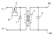
以下、図面を参照してこの発明の実施の形態について説明する。図1は、実施の形態に係る電力変換装置の一例を示す回路図である。図5に示す従来装置と同一部分には同一符号を付して、それらの説明は省略する。 Embodiments of the present invention will be described below with reference to the drawings. FIG. 1 is a circuit diagram illustrating an example of a power converter according to an embodiment. Parts identical to those of the conventional apparatus shown in FIG.
図1の電力変換装置では、共通のコアに巻かれた第1、第2の巻線9a,9bを有するインダクタ9が整流回路4とスイッチ素子6の間に設けられ、昇圧コイルとして機能している。第1の巻線9aは、整流回路4の電圧供給側ラインにダイオード7と接続するように配置され、第2の巻線9bは、整流回路4のマイナス側ラインを負荷20の接地側に接続するように配置されている。ここでは、第1、第2の巻線9aおよび9bは同一コアに同一巻数だけ巻かれている。
In the power conversion device of FIG. 1, an
スイッチ素子6がオンすると、インダクタ9の巻線9aおよび巻線9bに電流が流れて、そのコアに磁束が発生する。このとき、それぞれ巻線9aと巻線9bが発生する磁束は、互いに逆方向になる。したがって、インダクタ9ではその主磁束が互いに打ち消しあって、漏れインダクタンス成分にエネルギーが蓄積される。
When the switch element 6 is turned on, a current flows through the winding 9a and the winding 9b of the
図2は、図1のインダクタを示す図であって、(a)は具体的なコイル形状を示す断面図、(b)はコアの形状を示す斜視図である。
図2(a)において、ボビン21の中間部分には絶縁体からなるセパレータ22が配置され、セパレータ22により左右に離間して第1、第2の巻線9aおよび9bが巻かれている。また、コア23は同図(b)に示すように「8」の字形状をなし、コア脚部23aがボビン21を貫通するように配置され、第1、第2の巻線9aおよび9bをコア23内に収納している。コア23は、たとえば同図(b)のようなE字型のコア23eとI字型のコア23iの組み合わせ、あるいは2つのE字型のコアの組み合わせなどで形成することができる。
2A and 2B are diagrams illustrating the inductor of FIG. 1, in which FIG. 2A is a cross-sectional view illustrating a specific coil shape, and FIG. 2B is a perspective view illustrating a core shape.
In FIG. 2A, a
ここで、インダクタ9の巻線9aおよび9bは、図1の巻線に対応するものであって、セパレータ22によって巻線9a,9bの結合度の低い疎結合となっていれば、インダクタ9に必要な漏れインダクタンス値が実現できる。ここで、疎結合とは第1の巻線9aと第2の巻線9bとの磁気的な結合係数の値が1以下であることを言い、たとえば結合係数の値が0.8などである。すなわち、結合係数が1以下であるということは、第1の巻線9aには鎖交しても第2の巻線9bには鎖交しない磁束が存在し、かつ第2の巻線9bには鎖交しても第1の巻線9aには鎖交しない磁束が存在することを意味する。したがって、こうした漏れインダクタンスの大きさについては、巻線9aと9bの巻数を調整し、あるいはセパレータ22の大きさなどによって両者の間の距離を調整することによって、コモンモード電流を抑制するために必要な数百μ〜数mH程度まで漏れインダクタンス値を増加することができる。
Here, the
図3は、図1のインダクタを構成する別のコイル形状を示す断面図である。
図2のコイル形状では、巻線9a,9bを左右に分割することによって漏れインダクタンスを持たせるようにしたが、コア33内で2つの巻線9a,9bを同心円状に疎結合することで漏れインダクタンス値を大きくしても構わない。
FIG. 3 is a cross-sectional view showing another coil shape constituting the inductor of FIG.
In the coil shape of FIG. 2, the
すなわち、共通のボビン31には、図3に示すように、ボビン31の内周側に第1の巻線9aを巻き、その外周側に絶縁体からなるセパレータ32を介して、巻線9aと同軸に第2の巻線9bを巻くようにしている。この場合は、セパレータ32の厚さを大きくすることで、インダクタ9の巻線9a,9bの結合を疎にして、漏れインダクタンス値を大きくすることができる。
That is, as shown in FIG. 3, the
図4は、別の電力変換装置の要部構成を示す回路図である。ここでは、本発明を降圧型チョッパとして構成している。なお、図1と同一部分には同一符号を付して、その説明は省略する。 FIG. 4 is a circuit diagram showing a main configuration of another power converter. Here, the present invention is configured as a step-down chopper. In addition, the same code | symbol is attached | subjected to FIG. 1 and an identical part, and the description is abbreviate | omitted.
入力端子1a,1bは整流回路4に接続され、出力端子20a,20bは負荷20と接続される。ここでは、スイッチ素子6が整流回路4に接続される入力端子1aに接続され、かつインダクタ9の第1の巻線9aがスイッチ素子6の出力側に挿入されている点で、図1の実施の形態とは異なっている。
The
このように構成された電力変換装置は、図1の場合と同様にインダクタ9の漏れインダクタンスをエネルギー蓄積要素として利用することで、インダクタ9を構成するコイルを小形化できるから、電源変換装置の小形化が可能である。
Since the power converter configured in this way can use the leakage inductance of the
なお、いずれの実施の形態においても、スイッチ素子6としてMOSFETを用いた場合を説明したが、それ以外のバイポーラトランジスタやIGBTなどの自己消弧形素子を用いてスイッチ素子6を構成することもできる。 In any of the embodiments, the case where a MOSFET is used as the switch element 6 has been described. However, the switch element 6 can be configured using other self-extinguishing elements such as bipolar transistors and IGBTs. .
また、図1,図4の電力変換装置の場合でも、図5の従来装置と同様に、コモンモードチョークコイル3に相当するコイルを補助的に設けてもよい。そうした補助的なコイルは、従来技術におけるコモンモードチョークコイル3より小規模なものであってもコモンモードノイズを有効に抑制できるから、電源変換装置の大きさを小形化することができる。
1 and 4, a coil corresponding to the common
1 交流電源
2 ノイズフィルタ
2a〜2c,8 コンデンサ
4a〜4d,7 ダイオード
6 スイッチ素子
6a PWM制御回路
9 インダクタ
9a,9b 巻線
10 スイッチング電源装置
20 負荷
21,31 ボビン
22,32 セパレータ
23,33 コア
DESCRIPTION OF
Claims (5)
前記コイルは、共通のコアに巻かれて互いに疎結合された第1、第2の巻線を備え、
前記コイルの漏れインダクタンス成分を主変換動作のエネルギー蓄積要素とするとともに、前記コイルの主インダクタンス成分を前記スイッチ素子のオンオフ動作に起因する伝導ノイズの抑制要素としたことを特徴とする電力変換装置。 It consists of a rectifier circuit that rectifies the AC power supply, a smoothing capacitor that smoothes the output, an inverter circuit, and an energy storage coil. The switch element is controlled on and off from the AC voltage, and the energy stored in the coil is converted to a DC voltage. In the power converter that outputs as
The coil includes first and second windings wound around a common core and loosely coupled to each other.
A power conversion apparatus comprising: a leakage inductance component of the coil as an energy storage element for a main conversion operation; and a main inductance component of the coil as a suppression element for conduction noise caused by an on / off operation of the switch element.
Priority Applications (2)
| Application Number | Priority Date | Filing Date | Title |
|---|---|---|---|
| JP2008091029A JP2009247121A (en) | 2008-03-31 | 2008-03-31 | Power conversion apparatus |
| US12/382,194 US8223512B2 (en) | 2008-03-31 | 2009-03-10 | Power converter having an inductor including a first set of windings and a second set of windings both wound on a common core |
Applications Claiming Priority (1)
| Application Number | Priority Date | Filing Date | Title |
|---|---|---|---|
| JP2008091029A JP2009247121A (en) | 2008-03-31 | 2008-03-31 | Power conversion apparatus |
Publications (1)
| Publication Number | Publication Date |
|---|---|
| JP2009247121A true JP2009247121A (en) | 2009-10-22 |
Family
ID=41116944
Family Applications (1)
| Application Number | Title | Priority Date | Filing Date |
|---|---|---|---|
| JP2008091029A Pending JP2009247121A (en) | 2008-03-31 | 2008-03-31 | Power conversion apparatus |
Country Status (2)
| Country | Link |
|---|---|
| US (1) | US8223512B2 (en) |
| JP (1) | JP2009247121A (en) |
Cited By (2)
| Publication number | Priority date | Publication date | Assignee | Title |
|---|---|---|---|---|
| JP2011193593A (en) * | 2010-03-12 | 2011-09-29 | Mitsubishi Electric Corp | Ac-dc converter and air conditioner |
| JP2015089323A (en) * | 2013-10-29 | 2015-05-07 | コヴィディエン リミテッド パートナーシップ | Resonant inverter with common mode choke |
Families Citing this family (6)
| Publication number | Priority date | Publication date | Assignee | Title |
|---|---|---|---|---|
| JP5376308B2 (en) * | 2009-06-03 | 2013-12-25 | 富士電機株式会社 | Power factor correction circuit |
| US9248747B2 (en) * | 2011-11-29 | 2016-02-02 | Valeo Systemes De Controle Moteur | Converter for an electrical circuit designed to supply electrical propulsion power on board a motor vehicle |
| US10842563B2 (en) | 2013-03-15 | 2020-11-24 | Covidien Lp | System and method for power control of electrosurgical resonant inverters |
| US9923324B2 (en) * | 2015-01-31 | 2018-03-20 | Ixys Corporation | AC line filter and AC-to-DC rectifier module |
| DE102017109499A1 (en) * | 2017-05-03 | 2018-11-08 | Valeo Siemens Eautomotive Germany Gmbh | inverter |
| WO2021234614A1 (en) * | 2020-05-20 | 2021-11-25 | Ngai Kit Franki Poon | Power supply apparatus |
Citations (3)
| Publication number | Priority date | Publication date | Assignee | Title |
|---|---|---|---|---|
| JPH11178342A (en) * | 1997-12-16 | 1999-07-02 | Canon Inc | Power supply unit, electronic apparatus, and step-down type rectification/smoothing circuit |
| JP2003234220A (en) * | 2002-02-06 | 2003-08-22 | Sony Corp | Switching transformer and switching power supply |
| JP2005086958A (en) * | 2003-09-11 | 2005-03-31 | Yokogawa Electric Corp | Switching power supply |
Family Cites Families (25)
| Publication number | Priority date | Publication date | Assignee | Title |
|---|---|---|---|---|
| US4441146A (en) * | 1982-02-04 | 1984-04-03 | Vicor Corporation | Optimal resetting of the transformer's core in single ended forward converters |
| JPS6251983A (en) | 1985-09-02 | 1987-03-06 | Hagiwara Yoshihide | Serum-free culture medium for cultivating human/human hybridoma |
| JPH04355906A (en) | 1991-02-20 | 1992-12-09 | Yokogawa Electric Corp | Choke coil and noise-reducing device for switching power supply |
| US5291382A (en) * | 1991-04-10 | 1994-03-01 | Lambda Electronics Inc. | Pulse width modulated DC/DC converter with reduced ripple current coponent stress and zero voltage switching capability |
| JP3049696B2 (en) | 1992-01-14 | 2000-06-05 | デンセイ・ラムダ株式会社 | Switching power supply |
| JPH07263262A (en) | 1994-03-25 | 1995-10-13 | Sony Corp | Composite ac reactor |
| JP3326655B2 (en) | 1994-09-30 | 2002-09-24 | ソニー株式会社 | Current resonant switching power supply |
| US6191676B1 (en) * | 1994-10-21 | 2001-02-20 | Spinel Llc | Apparatus for suppressing nonlinear current drawing characteristics |
| JPH10150332A (en) | 1996-11-15 | 1998-06-02 | Nec Corp | Differential circuit |
| US5991170A (en) * | 1998-02-03 | 1999-11-23 | Sony Corporation | Equipment and method for transmitting electric power |
| JP2001268920A (en) | 2000-03-15 | 2001-09-28 | Tokin Corp | Active filter and dc appliance |
| JP3633892B2 (en) * | 2001-09-05 | 2005-03-30 | Fdk株式会社 | choke coil |
| JP4085234B2 (en) * | 2001-09-28 | 2008-05-14 | サンケン電気株式会社 | Switching power supply |
| JP2003153542A (en) | 2001-11-12 | 2003-05-23 | Cosel Co Ltd | Active-type power factor improving circuit |
| JP2004140006A (en) * | 2002-10-15 | 2004-05-13 | Minebea Co Ltd | Common mode choke coil and line filter |
| JP2004274161A (en) * | 2003-03-05 | 2004-09-30 | Tdk Corp | Noise suppression circuit |
| JP2004297551A (en) | 2003-03-27 | 2004-10-21 | Tdk Corp | Noise filter device and switching power supply |
| CN101436828B (en) * | 2003-04-22 | 2012-05-09 | 三垦电气株式会社 | Power factor improving circuit |
| US7598839B1 (en) * | 2004-08-12 | 2009-10-06 | Pulse Engineering, Inc. | Stacked inductive device and methods of manufacturing |
| JP4403926B2 (en) * | 2004-08-30 | 2010-01-27 | サンケン電気株式会社 | DC power supply |
| US20070252659A1 (en) * | 2004-10-14 | 2007-11-01 | Hiroshi Suenaga | Filter Circuit, Differential Transmission System Having Same, and Power Supply |
| JP3823322B2 (en) | 2005-05-26 | 2006-09-20 | 横河電機株式会社 | Distributed constant structure |
| FR2887704B1 (en) * | 2005-06-27 | 2007-08-10 | Agence Spatiale Europeenne | VOLTAGE REGULATOR CONVERTER WITHOUT SWITCHING LOSSES |
| US7327178B2 (en) * | 2005-09-30 | 2008-02-05 | Honeywell International, Inc. | Timing control circuit for lossless switching converter |
| JP2007235580A (en) | 2006-03-01 | 2007-09-13 | Toshiba Corp | Noise filter |
-
2008
- 2008-03-31 JP JP2008091029A patent/JP2009247121A/en active Pending
-
2009
- 2009-03-10 US US12/382,194 patent/US8223512B2/en not_active Expired - Fee Related
Patent Citations (3)
| Publication number | Priority date | Publication date | Assignee | Title |
|---|---|---|---|---|
| JPH11178342A (en) * | 1997-12-16 | 1999-07-02 | Canon Inc | Power supply unit, electronic apparatus, and step-down type rectification/smoothing circuit |
| JP2003234220A (en) * | 2002-02-06 | 2003-08-22 | Sony Corp | Switching transformer and switching power supply |
| JP2005086958A (en) * | 2003-09-11 | 2005-03-31 | Yokogawa Electric Corp | Switching power supply |
Cited By (3)
| Publication number | Priority date | Publication date | Assignee | Title |
|---|---|---|---|---|
| JP2011193593A (en) * | 2010-03-12 | 2011-09-29 | Mitsubishi Electric Corp | Ac-dc converter and air conditioner |
| JP2015089323A (en) * | 2013-10-29 | 2015-05-07 | コヴィディエン リミテッド パートナーシップ | Resonant inverter with common mode choke |
| US10898257B2 (en) | 2013-10-29 | 2021-01-26 | Covidien Lp | Resonant inverter with a common mode choke |
Also Published As
| Publication number | Publication date |
|---|---|
| US8223512B2 (en) | 2012-07-17 |
| US20090244943A1 (en) | 2009-10-01 |
Similar Documents
| Publication | Publication Date | Title |
|---|---|---|
| JP3861871B2 (en) | Switching power supply | |
| US8008886B2 (en) | Power converter | |
| US7209024B2 (en) | Filter circuit and power supply unit | |
| US8169796B2 (en) | Isolated switching power supply apparatus | |
| JP5585408B2 (en) | Switching power supply | |
| JP2009247121A (en) | Power conversion apparatus | |
| US20100165671A1 (en) | Switched-mode Power Supplies | |
| US6191965B1 (en) | Switching power supply | |
| JP5018960B2 (en) | Isolated switching power supply | |
| CN111492568B (en) | Interleaved LLC Resonant Converter | |
| KR20190016479A (en) | DC / DC converter | |
| KR101934446B1 (en) | Integrated magnetic circuit and the method of reducing magnetic density by shifting phase | |
| JP3402361B2 (en) | Switching power supply | |
| US20110199802A1 (en) | Single ended power converters operating over 50% duty cycle | |
| JP2014079108A (en) | Switching power-supply device | |
| JP2010124567A (en) | Switching power supply device | |
| JPWO2017002550A1 (en) | Power circuit | |
| JP2009017714A (en) | Switching power circuit | |
| JPWO2018123552A1 (en) | Snubber circuit and power conversion system using the same | |
| JP6393962B2 (en) | Switching power supply | |
| JP3882809B2 (en) | Switching power supply | |
| KR102144616B1 (en) | Isolation dc-dc converter using coupled-inductor | |
| JP2006191706A (en) | Dc converter | |
| JP2008172894A (en) | Switching power supply circuit | |
| JP2016158422A (en) | Forward type dc-dc converter circuit |
Legal Events
| Date | Code | Title | Description |
|---|---|---|---|
| A711 | Notification of change in applicant |
Free format text: JAPANESE INTERMEDIATE CODE: A712 Effective date: 20091112 |
|
| RD03 | Notification of appointment of power of attorney |
Free format text: JAPANESE INTERMEDIATE CODE: A7423 Effective date: 20091112 |
|
| RD04 | Notification of resignation of power of attorney |
Free format text: JAPANESE INTERMEDIATE CODE: A7424 Effective date: 20091112 |
|
| A625 | Written request for application examination (by other person) |
Free format text: JAPANESE INTERMEDIATE CODE: A625 Effective date: 20110315 |
|
| A711 | Notification of change in applicant |
Free format text: JAPANESE INTERMEDIATE CODE: A712 Effective date: 20110422 |
|
| A977 | Report on retrieval |
Free format text: JAPANESE INTERMEDIATE CODE: A971007 Effective date: 20120810 |
|
| A131 | Notification of reasons for refusal |
Free format text: JAPANESE INTERMEDIATE CODE: A131 Effective date: 20120814 |
|
| A02 | Decision of refusal |
Free format text: JAPANESE INTERMEDIATE CODE: A02 Effective date: 20121218 |