EP2566033A2 - Power conversion apparatus - Google Patents
Power conversion apparatus Download PDFInfo
- Publication number
- EP2566033A2 EP2566033A2 EP12181014A EP12181014A EP2566033A2 EP 2566033 A2 EP2566033 A2 EP 2566033A2 EP 12181014 A EP12181014 A EP 12181014A EP 12181014 A EP12181014 A EP 12181014A EP 2566033 A2 EP2566033 A2 EP 2566033A2
- Authority
- EP
- European Patent Office
- Prior art keywords
- voltage
- current
- power
- phase
- output
- Prior art date
- Legal status (The legal status is an assumption and is not a legal conclusion. Google has not performed a legal analysis and makes no representation as to the accuracy of the status listed.)
- Withdrawn
Links
Images


Classifications
-
- H—ELECTRICITY
- H02—GENERATION; CONVERSION OR DISTRIBUTION OF ELECTRIC POWER
- H02M—APPARATUS FOR CONVERSION BETWEEN AC AND AC, BETWEEN AC AND DC, OR BETWEEN DC AND DC, AND FOR USE WITH MAINS OR SIMILAR POWER SUPPLY SYSTEMS; CONVERSION OF DC OR AC INPUT POWER INTO SURGE OUTPUT POWER; CONTROL OR REGULATION THEREOF
- H02M1/00—Details of apparatus for conversion
- H02M1/12—Arrangements for reducing harmonics from ac input or output
-
- H—ELECTRICITY
- H02—GENERATION; CONVERSION OR DISTRIBUTION OF ELECTRIC POWER
- H02M—APPARATUS FOR CONVERSION BETWEEN AC AND AC, BETWEEN AC AND DC, OR BETWEEN DC AND DC, AND FOR USE WITH MAINS OR SIMILAR POWER SUPPLY SYSTEMS; CONVERSION OF DC OR AC INPUT POWER INTO SURGE OUTPUT POWER; CONTROL OR REGULATION THEREOF
- H02M7/00—Conversion of ac power input into dc power output; Conversion of dc power input into ac power output
- H02M7/42—Conversion of dc power input into ac power output without possibility of reversal
- H02M7/44—Conversion of dc power input into ac power output without possibility of reversal by static converters
- H02M7/48—Conversion of dc power input into ac power output without possibility of reversal by static converters using discharge tubes with control electrode or semiconductor devices with control electrode
-
- H—ELECTRICITY
- H02—GENERATION; CONVERSION OR DISTRIBUTION OF ELECTRIC POWER
- H02M—APPARATUS FOR CONVERSION BETWEEN AC AND AC, BETWEEN AC AND DC, OR BETWEEN DC AND DC, AND FOR USE WITH MAINS OR SIMILAR POWER SUPPLY SYSTEMS; CONVERSION OF DC OR AC INPUT POWER INTO SURGE OUTPUT POWER; CONTROL OR REGULATION THEREOF
- H02M1/00—Details of apparatus for conversion
- H02M1/0067—Converter structures employing plural converter units, other than for parallel operation of the units on a single load
- H02M1/007—Plural converter units in cascade
-
- H—ELECTRICITY
- H02—GENERATION; CONVERSION OR DISTRIBUTION OF ELECTRIC POWER
- H02M—APPARATUS FOR CONVERSION BETWEEN AC AND AC, BETWEEN AC AND DC, OR BETWEEN DC AND DC, AND FOR USE WITH MAINS OR SIMILAR POWER SUPPLY SYSTEMS; CONVERSION OF DC OR AC INPUT POWER INTO SURGE OUTPUT POWER; CONTROL OR REGULATION THEREOF
- H02M7/00—Conversion of ac power input into dc power output; Conversion of dc power input into ac power output
- H02M7/42—Conversion of dc power input into ac power output without possibility of reversal
- H02M7/44—Conversion of dc power input into ac power output without possibility of reversal by static converters
- H02M7/48—Conversion of dc power input into ac power output without possibility of reversal by static converters using discharge tubes with control electrode or semiconductor devices with control electrode
- H02M7/53—Conversion of dc power input into ac power output without possibility of reversal by static converters using discharge tubes with control electrode or semiconductor devices with control electrode using devices of a triode or transistor type requiring continuous application of a control signal
- H02M7/537—Conversion of dc power input into ac power output without possibility of reversal by static converters using discharge tubes with control electrode or semiconductor devices with control electrode using devices of a triode or transistor type requiring continuous application of a control signal using semiconductor devices only, e.g. single switched pulse inverters
- H02M7/5387—Conversion of dc power input into ac power output without possibility of reversal by static converters using discharge tubes with control electrode or semiconductor devices with control electrode using devices of a triode or transistor type requiring continuous application of a control signal using semiconductor devices only, e.g. single switched pulse inverters in a bridge configuration
- H02M7/53871—Conversion of dc power input into ac power output without possibility of reversal by static converters using discharge tubes with control electrode or semiconductor devices with control electrode using devices of a triode or transistor type requiring continuous application of a control signal using semiconductor devices only, e.g. single switched pulse inverters in a bridge configuration with automatic control of output voltage or current
- H02M7/53875—Conversion of dc power input into ac power output without possibility of reversal by static converters using discharge tubes with control electrode or semiconductor devices with control electrode using devices of a triode or transistor type requiring continuous application of a control signal using semiconductor devices only, e.g. single switched pulse inverters in a bridge configuration with automatic control of output voltage or current with analogue control of three-phase output
- H02M7/53876—Conversion of dc power input into ac power output without possibility of reversal by static converters using discharge tubes with control electrode or semiconductor devices with control electrode using devices of a triode or transistor type requiring continuous application of a control signal using semiconductor devices only, e.g. single switched pulse inverters in a bridge configuration with automatic control of output voltage or current with analogue control of three-phase output based on synthesising a desired voltage vector via the selection of appropriate fundamental voltage vectors, and corresponding dwelling times
Definitions
- the present invention relates to a power conversion apparatus.
- Power conversion apparatuses include a power converter to convert power from a power source into alternating-current (AC) power and to output the AC power to a power system.
- Examples of the power conversion apparatuses include system-interconnection inverters.
- the inverters convert direct-current (DC) power from solar cells, fuel cells, and other power sources into AC power and output the AC power to a power system.
- Japanese Patent No. 3023647 discloses such a power conversion apparatus.
- the power conversion apparatus detects DC components contained in output current of the power converter and reflects the result of detection on a current feedback system, in an attempt to remove the DC components of the output current.
- Conventional power conversion apparatuses employ a current detector to detect the output current for use in the current feedback.
- Current detectors output detection signals that contain noise such as carrier components. Noise makes it difficult to set the gain of the current feedback control at a level high enough to remove the DC components of the output current.
- a power conversion apparatus includes a power converter, a voltage detector, a current detector, a detection voltage adjustor, and a controller.
- the power converter is configured to convert power from a power source into alternating-current power and is configured to output the alternating-current power to a power system.
- the voltage detector is configured to detect a voltage of the power system.
- the current detector is configured to detect a direct-current component of a current between the power converter and the power system.
- the detection voltage adjustor is configured to add a DC correction (hereinafter referred to as a bias) corresponding to the direct-current component to the voltage detected by the voltage detector, so as to generate a voltage detection signal, and is configured to output the voltage detection signal.
- the controller is configured to control the power converter to output an alternating-current voltage corresponding to the voltage detection signal.
- the embodiment provides a power conversion apparatus that efficiently removes DC components contained in output current.
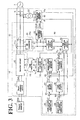
- FIG. 1 is a diagram illustrating a first embodiment of the power conversion apparatus.
- a power conversion apparatus 1 according to the first embodiment is disposed between a power source 2 and a power system 3.
- the power conversion apparatus 1 converts power from the power source 2 into AC power and outputs the AC power to the power system 3.
- Examples of the power source 2 include, but not limited to, a generating apparatus and a fuel cell to convert natural energy, such as sunlight and wind, into electrical energy.
- the power conversion apparatus 1 includes a power converter 10, a voltage detector 20, a current detector 30, a detection voltage adjustor 40, and a controller 50.
- the power converter 10 outputs AC voltage (hereinafter referred to as output voltage), which is controlled based on the voltage of the power system 3. This ensures power supply from the power conversion apparatus 1 to the power system 3.
- the power converter 10 converts power from the power source 2 into AC power and outputs the AC power to the power system 3.
- the power from the power source 2 is DC power
- examples of the power converter 10 to be used include, but not limited to, an inverter circuit to convert DC power into AC power.
- the voltage detector 20 detects the voltage of the power system 3. The result of detection is used to control the phase and the amplitude of output voltage of the power converter 10.
- the current detector 30 includes a current detection section 31 and a DC component detection section 32.
- the current detection section 31 detects currents (hereinafter referred to as output currents) supplied from the power converter 10 to the power system 3.
- the DC component detection section 32 detects DC components contained in phase currents detected by the current detection section 31, and outputs the result of detection to the detection voltage adjustor 40.
- the detection voltage adjustor 40 generates voltage detection signals using the detection output of the voltage detector 20 and using biases that are based on the respective DC components detected by the DC component detection section 32. The detection voltage adjustor 40 then outputs the voltage detection signals to the controller 50.
- the factors behind DC components being contained in the output currents include variations between the elements constituting the power converter 10.
- the controller 50 carries out current feedback control to make a match between a target current value and each output current detected by the current detector 30.
- Each of the voltage detection signals output from the detection voltage adjustor 40 is added to the output of the current feedback control, generating an output voltage command.
- the controller 50 controls the power converter 10 to output voltages each of which is the sum of the voltage of the power system 3 and a bias voltage corresponding to a DC component among the DC components of the output currents of the power converter 10. This accurately eliminates or minimizes DC components contained in the output currents.
- FIG. 2 is a diagram illustrating a simplified model of the power converter 10 and the power system 3, where the three-phase AC voltages are line voltages. The sum of the three line voltages supplied by the power converter 10 is zero.
- the simplified model shown in FIG. 2 employs two AC power sources VA and VB with the power system 3 as a load. Since the following description is regarding a DC component, the impedance of the power system 3 is taken into consideration only on the resistance part, and resistances R r , R s , and R t respectively of the R, S, and T phases are assumed equal to each other and collectively designated at R.
- the single-phase AC power sources VA and VB respectively have DC components V 1dc and V 2dc , which are obtained by Formulae (1) and (2).
- V 1 ⁇ dc R ⁇ 2 ⁇ I rdc + I tdc
- V 2 ⁇ dc R ⁇ I rdc + 2 ⁇ I tdc
- I rdc denotes a DC component occurring in a current I r flowing from the positive pole of the single-phase AC power source VA to the R phase
- I tdc denotes a DC component occurring in a current I t flowing from the positive pole of the single-phase AC power source VB to the T phase.
- the DC components V 1dc and V 2dc occur respectively in the single-phase AC power sources VA and VB
- the DC components V 1dc and V 2dc respectively cause the DC components I rdc and I tdc to occur.
- the DC components I rdc and I tdc are detected by the DC component detection section 32.
- the voltage detector 20 detects voltages V 1 and V 2 respectively of the single-phase AC power sources VA and VB.
- the detection voltage adjustor 40 adds bias voltages - V 1dc and - V 2dc respectively to the voltages V 1 and V 2 , thereby generating voltage detection signals.
- the bias voltages -V 1dc and -V 2dc respectively correspond to the DC components I rdc and I tdc detected by the DC component detection section 32.
- the controller 50 controls the single-phase AC power source VA to output a voltage that is the sum of the voltage V 1 and the bias voltage -V 1dc , and controls the single-phase AC power source VB to output a voltage that is the sum of the voltage V 2 and the bias voltage - V 2dc . This ensures removal of the DC components I rdc and I tdc respectively from the currents I r and I t .
- the power conversion apparatus 1 eliminates or minimizes the DC components of the output currents, and ensures improved quality of power output to the power system 3.
- the power system 3 can be influenced by, for example, DC magnetization of a pole transformer.
- the power converter 10 supplies three-phase AC power, this should not be construed in a limiting sense.
- the power conversion apparatus may output single-phase AC power.
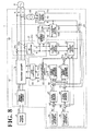
- FIG. 3 is a diagram illustrating a detailed configuration of the power conversion apparatus 1 according to the first embodiment.
- the power conversion apparatus 1 includes the power converter 10, the voltage detector 20, the current detector 30, the detection voltage adjustor 40, and the controller 50.
- the power converter 10 includes a boost chopper circuit 11 and an inverter circuit 12.
- the boost chopper circuit 11 boosts a DC voltage V dc output from the power source 2 and outputs the boosted DC voltage V dc to the inverter circuit 12.
- the boost chopper circuit 11 may not be necessary if the DC voltage V dc output from the power source 2 is convertible into the voltage of the power system 3 by the inverter circuit 12.
- FIG. 4 is a diagram illustrating the power converter 10.
- the boost chopper circuit 11 includes a capacitor C10, a coil L10, a semiconductor switch element Q10, and diodes D10 and D11.
- the semiconductor switch element Q10 is controlled between its on state and off state by the controller 50. This ensures that a DC voltage V pn , which is boosted by the boost chopper circuit 11, is output to the inverter circuit 12.
- Examples of the semiconductor switch element Q10 include, but not limited to, a power semiconductor device such as IGBT and MOSFET.
- the boost chopper circuit 11, not limited to the configuration shown in FIG. 4 may be modified in various other manners.
- the inverter circuit 12 includes capacitors C20 to C23, semiconductor switch elements Q20 to Q23, diodes D20 to D23, and coils L20 and L21.
- the semiconductor switch elements Q20 to Q23 are controlled between their on state and off state by the controller 50. This ensures that the inverter circuit 12 converts the DC voltage V pn into the voltage of the power system 3.
- Examples of the semiconductor switch elements Q20 to Q23 include, but not limited to, power semiconductor devices such as IGBT and MOSFET.
- the inverter circuit 12, not limited to the 2-level inverter shown in FIG. 4 may be a multi-level inverter or may be modified in various other manners.
- the power from the power source 2 is DC power
- the power converter 10 includes an inverter circuit.
- the power converter 10 to be used include, but not limited to, a converter circuit together with an inverter circuit.
- the converter circuit would convert the AC power from the power source 2 into DC power
- the inverter circuit would convert the DC power output from the converter circuit into AC power that corresponds to the voltage of the power system 3. It is also possible to use a rectifier in place of the converter circuit.
- the voltage detector 20 has its input side coupled to the phases of the power system 3 so as to detect instantaneous values of the line voltage of the power system 3. Specifically, the voltage detector 20 detects an instantaneous value V rs of the line voltage between the R phase and the S phase (hereinafter referred to as R-S line voltage V rs ), and an instantaneous value V ts of the line voltage between the T phase and the S phase (hereinafter referred to as T-S line voltage V ts ).
- the current detector 30 includes the current detection section 31 and the DC component detection section 32.
- the current detection section 31 includes current detection sub-sections 31a and 31b, and an AD converter 31c.
- the current detection sub-section 31a detects an instantaneous value I r of the R-phase current between the power converter 10 and the R phase of the power system 3 (the instantaneous value I r being hereinafter referred to as R-phase current I r ).
- the current detection sub-section 31b detects an instantaneous value I t of the T-phase current between the power converter 10 and the T phase of the power system 3 (the instantaneous value I t being hereinafter referred to as T-phase current I t ).
- the R-phase current I r and the T-phase current I t respectively detected by the current detection sub-sections 31a and 31b are input into the AD converter 31c, which in turn digitizes the R-phase current I r and the T-phase current I t .
- the DC component detection section 32 detects a DC component of the R-phase current and a DC component of the T-phase current, and generates an R-phase bias voltage V rdc and a T-phase bias voltage V tdc .
- the R-phase bias voltage V rdc corresponds to the DC component of the R-phase current
- the T-phase bias voltage V tdc corresponds to the DC component of the T-phase current.
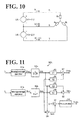
- FIG. 5 is a diagram illustrating the DC component detection section 32.
- the DC component detection section 32 includes moving-average operators 61a and 61b, lowpass filters 62a and 62b, amplifiers 63 to 66, and adders 67 and 68.
- the moving-average operator 61a obtains a moving average of the values of the R-phase current I r . Specifically, the moving-average operator 61a obtains an average of the values of the R-phase current I r per current period of the power system 3, and outputs the average as a moving-average signal I r av of the R-phase current I r .
- the moving-average operator 61b obtains a moving average of the values of the T-phase current I t . Specifically, the moving-average operator 61b obtains an average of the values of the T-phase current I t per current period of the power system 3, and outputs the average as a moving-average signal I tav of the T-phase current I t .
- the lowpass filter 62a removes high-frequency components of the moving-average signal I rav output from the moving-average operator 61a so as to detect the DC component I rdc of the R-phase current I r .
- the lowpass filter 62a then outputs the DC component I rdc to the amplifiers 63 and 65.
- the amplifier 63 amplifies the DC component I rdc of the R-phase current I r at an amplification ratio K 1 , and outputs the amplified DC component I rdc to the adder 67.
- the amplifier 65 amplifies the DC component I rdc of the R-phase current I r at an amplification ratio K 3 , and outputs the amplified DC component I rdc to the adder 68.
- the lowpass filter 62a is a primary delay lowpass filter with, in the first embodiment, a time constant T of 400 ms.
- Formula (1) shows that in the first embodiment, the amplification ratio K 1 is "2R", while the amplification ratio K 3 is "R".
- the lowpass Niter 62b removes high-frequency components of the moving-average signal I tav output from the moving-average operator 61b so as to detect the DC component I tdc of the T-phase current I t .
- the lowpass filter 62b then outputs the DC component I tdc to the amplifiers 64 and 66.
- the amplifier 64 amplifies the DC component I tdc of the T-phase current I t at an amplification ratio K 2 , and outputs the amplified DC component I tdc to the adder 67.
- the amplifier 66 amplifies the DC component I tdc of the T-phase current I t at an amplification ratio K 4 , and outputs the amplified DC component I tdc to the adder 68.
- the lowpass filter 62b is a primary delay lowpass filter with, in the first embodiment, a time constant T of 400 ms.
- Formula (2) shows that in the first embodiment, the amplification ratio K 2 is "R", while the amplification ratio K 4 is "2R".
- the adder 67 calculates the sum of the outputs of the amplifiers 63 and 64 so as to generate the R-phase bias voltage V rdc .
- the adder 67 generates the R-phase bias voltage V rdc based on Formula (1) using the DC component I rdc of the R-phase current I r and using the DC component I tdc of the T-phase current I t .
- the adder 68 calculates the sum of the outputs of the amplifiers 65 and 66 so as to generate the T-phase bias voltage V tdc .
- the adder 68 generates the T-phase bias voltage V tdc based on Formula (2) using the DC component I rdc of the R-phase current I r and using the DC component I tdc of the T-phase current I t .
- the DC component detection section 32 includes the moving-average operators 61a and 61b, the lowpass filters 62a and 62b, the amplifiers 63 to 66, and the adders 67 and 68.
- the DC component detection section 32 detects the DC components I rdc and I tdc respectively contained in the R-phase current I r and the T-phase current I t .
- the DC component detection section 32 then detects the R-phase bias voltage V rdc and the T-phase bias voltage V tdc respectively based on the DC components I rdc and I tdc .
- the DC component detection section 32 shown in FIG. 5 is for exemplary purposes only and open to various modifications.
- the moving averages obtained by the moving-average operators 61a and 61b may be per a plurality of current periods. This eliminates the need for the lowpass filters 62a and 62b.
- the detection voltage adjustor 40 obtains a q-axis voltage detection signal V q and a phase ⁇ based on the R-S line voltage V rs , the T-S line voltage V ts , the R-phase bias voltage V rdc , and the T-phase bias voltage V tdc .
- FIG. 6 is a diagram illustrating the detection voltage adjustor 40.
- the detection voltage adjustor 40 includes subtractors 71 and 72, a d-q coordinate system converter 73, and a phase operator 74.
- the subtractor 71 subtracts the R-phase bias voltage V rdc from the R-S line voltage V rs so as to obtain the R-phase voltage detection signal V rsa .
- the subtractor 71 then outputs the R-phase voltage detection signal V rsa to the d-q coordinate system converter 73, which is a rotational coordinate system converter.
- the subtractor 72 subtracts the T-phase, bias voltage V tdc from the T-S line voltage V ts so as to obtain the T-phase voltage detection signal V tsa .
- the subtractor 72 then outputs the T-phase voltage detection signal V tsa to the d-q coordinate system converter 73, which is a rotational coordinate system converter.
- the d-q coordinate system converter 73 Based on a phase ⁇ obtained by the phase operator 74 described later, the d-q coordinate system converter 73 converts the output of the subtractor 71 and the output of the subtractor 72 into d-q components of a d-q coordinate system. In this manner, the d-q coordinate system converter 73 obtains the q-axis voltage detection signal V q and a d-axis voltage detection signal V d . As described later, the phase ⁇ is generated such that the d-axis voltage detection signal V d has a value of zero. The d-q coordinate system converter 73, therefore, outputs the q-axis voltage detection signal V q alone as a detection value of the power amplitude of the power system 3.
- the phase operator 74 obtains the phase ⁇ based on the q-axis voltage detection signal V q and the d-axis voltage detection signal V d output from the d-q coordinate system converter 73.
- the phase ⁇ is determined to make the d-axis voltage detection signal V d zero, and the determined phase ⁇ is used by the d-q coordinate system converter 73 for the conversion into the d-q components of the d-q coordinate system.
- the phase operator 74 carries out closed loop control as described above so as to generate the phase ⁇ , and outputs the phase ⁇ as a detection value of the voltage phase of the power system 3.
- the detection voltage adjustor 40 shown in FIG. 6 is for exemplary purposes only, and other examples of the detection voltage adjustor 40 include the configuration shown in FIG. 7 .
- the detection voltage adjustor 40 shown in FIG. 7 includes a phase locked loop (PLL) circuit 75 in place of the phase operator 74.
- PLL phase locked loop
- the PLL circuit 75 includes a phase detector 100, a filter 101, a voltage control oscillator (VCO) 102, a frequency divider 103, a counter 104, a zero-cross rising detector 105, and an adder 106.
- VCO voltage control oscillator
- the phase detector 100 compares the T-phase voltage detection signal V tsa with a frequency division signal output through an open loop from the frequency divider 103 so as to detect and output a phase difference.
- the filter 101 is a lowpass filter to set a loop time constant of the PLL circuit 75.
- the voltage control oscillator 102 outputs a pulse signal having a frequency corresponding to a voltage output from the filter 101.
- the frequency divider 103 divides the output signal of the voltage control oscillator 102 into 1/N. This ensures that the output of the voltage control oscillator 102 has a frequency that is N times the frequency of the input signal of the voltage control oscillator 102.
- the counter 104 receives the output signal of the voltage control oscillator 102 so as to count the pulse number of the received output signal.
- the zero-cross rising detector 105 detects the timing of zero-crossing of the T-phase voltage detection signal V tas during its rising. When zero-crossing of the T-phase voltage detection signal V tsa occurs during its rising, the zero-cross rising detector 105 outputs a reset signal to the counter 104. This ensures that the counter 104 generates a phase ⁇ c counted from the timing of the zero-crossing of the T-phase voltage detection signal V tsa that occurred during its rising.
- the adder 106 adds ⁇ corresponding to the T-phase voltage detection signal V tsa .
- the adder 106 then outputs the sum as the phase ⁇ of the power system 3.
- ⁇ corresponding to the T-phase voltage detection signal V tsa refers to a value at which the d-axis voltage detection signal V d generated by the d-q coordinate system converter 73 has a value of zero.
- the detection voltage adjustor 40 may use the PLL circuit 75 in place of the phase operator 74.
- the PLL circuit 75 may receive the R-phase voltage detection signal V rsa instead of the T-phase voltage detection signal V tsa .
- ⁇ to be added to the phase ⁇ c output from the counter 104 corresponds to the R-phase voltage detection signal V rsa .
- ⁇ corresponding to the R-phase voltage detection signal V rsa refers to a value at which the d-axis voltage detection signal V d generated by the d-q coordinate system converter 73 has a value of zero.
- the controller 50 includes an ⁇ - ⁇ coordinate system converter 81 and a d-q coordinate system converter 82.
- the ⁇ - ⁇ coordinate system converter 81 converts the R-phase current I r and the T-phase current I t respectively into an ⁇ component and a ⁇ component.
- the ⁇ - ⁇ components are coordinates of a fixed coordinate system defined by two perpendicular axes. In this manner, the ⁇ - ⁇ coordinate system converter 81 obtains a fixed coordinate current vector I ⁇ of the ⁇ - ⁇ coordinate system, with a current I ⁇ in the ⁇ axis direction and a current I ⁇ in the ⁇ axis direction as vector components.
- the d-q coordinate system converter 82 uses the phase ⁇ output from the detection voltage adjustor 40 to convert the fixed coordinate current vector I ⁇ into d-q components of a d-q coordinate system. In this manner, the d-q coordinate system converter 82 obtains a rotational coordinate system current vector I dq ( I d , I q ) , with a q-axis current I q and a d-axis current I d as vector components.
- the q-axis current I q is a current value in the q axis direction
- the d-axis current I d is a current value in the d axis direction.
- the d-q coordinate system is a coordinate system rotated relative to the ⁇ - ⁇ coordinate system by a degree corresponding to the phase ⁇ .
- the controller 50 further includes a q-axis current command output device 83, a d-axis current command output device 84, a q-axis current deviation operator 85, a d-axis current deviation operator 86, a q-axis current adjuster 87, a d-axis current adjuster 88, and a q-axis voltage command corrector 89.
- the controller 50 further includes an output voltage command generator 90, an output phase command generator 91, an adder 92, an inverse rotational coordinate system converter 93, and a PWM control device 94.
- the q-axis current command output device 83 generates a q-axis current command I q * and outputs the q-axis current command I q * to the q-axis current deviation operator 85.
- the q-axis current command I q * is a target value of active current.
- the q-axis current deviation operator 85 calculates the deviation of the q-axis current I q from the q-axis current command I q * as a q-axis current deviation, and outputs the q-axis current deviation to the q-axis current adjuster 87.
- the q-axis current adjuster 87 adjusts a q-axis voltage command V q1 * to make the deviation of the q-axis current I q from the q-axis current command I q * zero.
- the q-axis current adjuster 87 then outputs the adjusted q-axis voltage command V q1 * to the q-axis voltage command corrector 89.
- the q-axis voltage command corrector 89 adds the q-axis voltage detection signal V q output from the detection voltage adjustor 40.
- the q-axis voltage command corrector 89 then outputs the sum as the q-axis voltage command V q * to the output voltage command generator 90 and the output phase command generator 91.
- the d-axis current command output device 84 generates a d-axis current command I d * and outputs the d-axis current command I d * to the d-axis current deviation operator 86.
- the d-axis current command I d * is a target value of reactive current.
- the d-axis current deviation operator 86 calculates the deviation of the d-axis current I d from the d-axis current command I d * as a d-axis current deviation, and outputs the d-axis current deviation to the d-axis current adjuster 88.
- the d-axis current adjuster 88 adjusts a d-axis voltage command V d * to make the deviation of the d-axis current I d from the d-axis current command I d * zero.
- the d-axis current adjuster 88 then outputs the adjusted d-axis voltage command V d * to the output voltage command generator 90 and the output phase command generator 91.
- the output voltage command generator 90 obtains an output voltage command V 1 * based on the q-axis voltage command V q * output from the q-axis voltage command corrector 89 and the d-axis voltage command V d * output from the d-axis current adjuster 88. Specifically, the output voltage command generator 90 uses, for example, Formula (3) to obtain the output voltage command V 1 * .
- Formula (3) is for exemplary purposes only and open to various modifications.
- Output voltage command V 1 * V d * 2 + V q * 2 1 / 2
- the output phase command generator 91 obtains an output phase command ⁇ a * based on the q-axis voltage command V q * output from the q-axis voltage command corrector 89 and the d-axis voltage command V d * output from the d-axis current adjuster 88. Specifically, the output phase command generator 91 uses, for example, Formula (4) to obtain the output phase command ⁇ a * .
- Output phase command ⁇ a * tan - 1 V q * / V d *
- the adder 92 adds the phase ⁇ output from the detection voltage adjustor 40 so as to calculate a phase ⁇ p .
- the inverse rotational coordinate system converter 93 obtains three-phase AC voltage commands.
- the three-phase AC voltage commands include an R-phase output voltage command V r * to the R phase of the power system 3, an S-phase output voltage command V s * to the S phase of the power system 3, and a T-phase output voltage command V t * to the T phase of the power system 3.
- the inverse rotational coordinate system converter 93 uses, for example, Formulae (5) to (7) to obtain the R-phase output voltage command V r * , the S-phase output voltage command V s * , and the T-phase output voltage command V t * .
- the PWM control device 94 is a control signal output device that outputs PWM command signals, which are control signals, to the power converter 10. Specifically, based on the output voltage commands V r * , V s * , and V t * output from the inverse rotational coordinate system converter 93 and based on the DC voltage V pn , the PWM control device 94 generates and outputs gate signals to control the semiconductor switch elements Q20 to Q23 of the power converter 10. This ensures that the power converter 10 outputs three-phase AC voltages corresponding to their respective output voltage commands V r * , V s * , and V t * .
- the power conversion apparatus 1 includes the detection voltage adjustor 40 and the controller 50.
- the detection voltage adjustor 40 adds bias voltages corresponding to the DC components detected by the current detector 30, thereby generating voltage detection signals.
- the controller 50 controls the power converter 10 to output AC voltages corresponding to the respective voltage detection signals. This ensures effective removal of DC components from the output currents. This, as a result, improves the quality of power output to the power system 3.
- the voltage detector 20 is illustrated as detecting an instantaneous value of the line voltage of the power system 3.
- the detection voltage adjustor 40 may have a function of converting the phase voltages into a line voltage. This another embodiment may otherwise be similar to the first embodiment.
- the R-phase voltage detection signal V rsa and the T-phase voltage detection signal V tsa are first obtained, and then they are converted onto a rotational coordinate system.
- the R-S line voltage V rs and the R-phase bias voltage V rdc may be converted onto a rotational coordinate system mutually separately, while the T-S line voltage V ts and the T-phase bias voltage V tdc may be converted onto the rotational coordinate system mutually separately.
- these converted voltages may serve as a basis on which to obtain the q-axis voltage detection signal V q and the d-axis voltage detection signal V d respectively corresponding to the R-phase voltage detection signal V rsa and the T-phase voltage detection signal V tsa .
- the power conversion apparatus 1 may include a d-q coordinate system converter 33 and adders 34 and 35.
- the d-q coordinate system converter 33 uses the phase ⁇ of the power system 3 to convert the R-phase bias voltage V rdc and the T-phase bias voltage V tdc into signals on a d-q coordinate system. In this manner, the d-q coordinate system converter 33 generates a q-axis voltage detection signal V q0 and a d-axis voltage detection signal V d0 .
- the adder 34 adds the q-axis voltage detection signal V q output from the detection voltage adjustor 40, thereby generating a q-axis voltage detection signal V q1 .
- the q-axis voltage command corrector 89 adds the q-axis voltage detection signal V q1 to the q-axis voltage command V q1 * , resulting in a q-axis voltage command V q * .
- the q-axis voltage command V q * is output to the output voltage command generator 90 and the output phase command generator 91.
- the adder 35 adds the q-axis voltage command output from the d-axis current adjuster 88, resulting in a d-axis voltage command V d * .
- the adder 35 outputs the d-axis voltage command V d * to the output voltage command generator 90 and the output phase command generator 91.
- the d-q coordinate system converter 33, the adders 34 and 35, and the detection voltage adjustor 40 constitute another detection voltage adjustor.
- the other detection voltage adjustor adds a bias voltage corresponding to a DC component detected by the current detector 30, thereby generating a voltage detection signal.
- the other detection voltage adjustor then outputs the voltage detection signal.
- no subtractors 71 and 72 are necessary for the detection voltage adjustor 40.
- the R-S line voltage V rs and the T-S line voltage V ts are directly input to the d-q coordinate system converter 73.
- the one detection voltage adjustor may generate the q-axis voltage detection signal V q and the voltage phase ⁇ from the detection voltage of the voltage detector 20.
- the other detection voltage adjustor may use the voltage phase ⁇ to generate the q-axis voltage detection signal V q0 and the d-axis voltage detection signal V d0 from the DC components detected by the DC component detection section 32. Then, the voltage detection signals may be subjected to addition.
- the output voltage command generator 90, the output phase command generator 91, the adder 92, and the inverse rotational coordinate system converter 93 are used to convert the voltage commands V d * and V q * of the rotational coordinate system into three-phase AC voltage commands, namely, the output voltage commands V r * , V s * , and V t * respectively to the R phase, the S phase, and the T phase of the power system 3.
- the conversion may be by the use of inverse converters dedicated to the ⁇ - ⁇ coordinate system converter 81 and the d-q coordinate system converter 82.
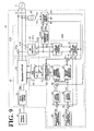
- FIGs. 9 to 11 A second embodiment of the power conversion apparatus will be described in detail by referring to FIGs. 9 to 11 .
- Like reference numerals designate corresponding or identical elements throughout FIGs. 3 , 5 , 9 , and 11 , and these elements will not be elaborated here.
- a power conversion apparatus 1 A includes a power converter 10, a voltage detector 20, a current detector 30A, a detection voltage adjustor 40, and a controller 50A.
- the power conversion apparatus 1A includes an adjustment loop to make a DC component I sdc of a S-phase current I s zero,
- FIG. 10 is a diagram illustrating a simplified model of the power converter 10 and the power system 3, similarly to FIC. 2.
- the power converter 10 serves as ideal single-phase AC power sources VA and VB, and the power system 3 serves as a load.
- the adjustment loop operates to make the DC component I sdc of the S-phase current I s zero. This results in a voltage adjustment of ⁇ V , turning the voltage of the single-phase AC power source VA from V 1 to V 1 + ⁇ V and turning the voltage of the single-phase AC power source VB from V 2 to V 2 + ⁇ V.
- the current detector 30A includes a current detection section 31 and a DC component detection section 32A.
- the DC component detection section 32A detects the DC components I rdc and I tdc respectively contained in the R-phase current I r and the T-phase current I t detected by the current detection section 31. Then, the DC component detection section 32A generates an R-phase bias voltage V rdc , a T-phase bias voltage V tdc , and an S-phase bias voltage V sdc corresponding to the DC components I rdc and I tdc .
- FIG. 11 is a diagram illustrating the DC component detection section 32A in detail.
- the DC component detection section 32A includes an adder 96, a subtractor 97, and a PI controller 98, in addition to the configuration of the DC component detection section 32 shown in FIG. 5 .
- the adder 96 adds the DC component I rdc of the R-phase current I r output from the lowpass filter 62a to the DC component I rdc of the T-phase current I t output from the lowpass filter 62b, and outputs the sum to the subtractor 97.
- the sum of instantaneous current values of the R phase, the S phase, and the T phase equals zero.
- the value of the DC component I sdc of the S-phase current I s and the sum of the values of the DC component I rdc of the R-phase current I r and the DC component I tdc of the T-phase current I t have the same numerical parts with opposite signs, plus or minus.
- the output of the adder 96 and the value of the DC component I sdc of the S-phase current I s have the same numerical parts with opposite signs, plus or minus.
- the DC component I sdc of the S-phase current I s has a value of zero
- the DC component I rdc of the R-phase current I r and the DC component I tdc of the T-phase current I t have the same absolute values.
- adjusting the output voltage of the power converter 10 based on either the R-phase bias voltage V rdc or the T-phase bias voltage V tdc results in both V 1dc and V 2dc respectively shown in Formulae (1) and (2) being adjusted.
- the DC component detection section 32A has the subtractor 97 subtract the output of the adder 96 from zero, and has the PI controller 98 subject the output of the subtractor 97 to proportional integration (PI) control, thereby generating the S-phase bias voltage V sdc .
- the PI controller 98 then outputs the S-phase bias voltage V sdc to the controller 50A.
- the controller 50A has its adder 95 add the S-phase bias voltage V sdc output from the PI controller 98 to the S-phase output voltage commands V s * output from the inverse rotational coordinate system converter 93. This ensures that the DC component I sdc of the S-phase current I s is controlled at zero.
- the power conversion apparatus 1A ensures that the DC component detection section 3 2A adjusts the output voltage of the power converter 10 based on either the R-phase bias voltage V rdc or the T-phase bias voltage V tdc . This ensures making the amplification ratios K 1 and K 2 respectively of the amplifiers 63 and 64 zero, or making the amplification ratios K 3 and K 4 respectively of the amplifiers 65 and 66 zero.
- the S-phase bias voltage V sdc may not necessarily be added to the S-phase output voltage command V s * . Instead, it is possible to carry out coordinate conversion of the S-phase bias voltage V sdc into a d-axis voltage and a q-axis voltage using the phase ⁇ . The d-axis voltage and the q-axis voltage then may be respectively added to the output of the d-axis current adjuster 88 and the output of the q-axis current adjuster 87.
- the DC component detection section 32A detects the DC component I sdc of the S-phase current Is from the DC component I rdc of the R-phase current I r and from the DC component I tdc of the T-phase current I t . It is also possible to provide the S phase with a current detector to directly detect the DC component I sdc of the S-phase current I s .
- the power conversion apparatus 1A is illustrated as including an adjustment loop to make the DC component I sdc of the S-phase current I s zero.
- the adjustment loop may make the DC component associated with the R phase or the T phase zero.
- the inverter circuit 12 has been illustrated as having a main circuit configuration with two arms, it is also possible to employ a main circuit configuration with three arms.
- the output voltage commands V r * , V s * , and V t * may be generated in the manner described in the above-described embodiments.
- the PWM control device 94 may output PWM command signals corresponding to the respective semiconductor switch elements of the inverter circuit 12. This configuration is otherwise approximately similar to the above-described embodiments.
- the power converter 10 may be a matrix converter to convert the AC power of the power source 2 into AC power accommodated to the voltage of the power system 3.
- the current control and the voltage control are based on conversion onto rotational coordinate systems. This, however, should not be construed in a limiting sense. For example, it is also possible to carry out the current control and the voltage control without conversion onto rotational coordinate systems.
Abstract
Description
- The present invention relates to a power conversion apparatus.
- Power conversion apparatuses include a power converter to convert power from a power source into alternating-current (AC) power and to output the AC power to a power system. Examples of the power conversion apparatuses include system-interconnection inverters. The inverters convert direct-current (DC) power from solar cells, fuel cells, and other power sources into AC power and output the AC power to a power system.
- Japanese Patent No.
3023647 - The contents of Japanese Patent No.
3023647 - Conventional power conversion apparatuses employ a current detector to detect the output current for use in the current feedback. Current detectors output detection signals that contain noise such as carrier components. Noise makes it difficult to set the gain of the current feedback control at a level high enough to remove the DC components of the output current.
- This has caused difficulty in removing a sufficient amount of DC components contained in the output current, even though the DC components contained in the output current are detected and reflected on the current feedback system.
- It is an object of an embodiment to provide a power conversion apparatus that efficiently removes DC components contained in the output current.
- According to one aspect of the present invention, a power conversion apparatus includes a power converter, a voltage detector, a current detector, a detection voltage adjustor, and a controller. The power converter is configured to convert power from a power source into alternating-current power and is configured to output the alternating-current power to a power system. The voltage detector is configured to detect a voltage of the power system. The current detector is configured to detect a direct-current component of a current between the power converter and the power system. The detection voltage adjustor is configured to add a DC correction (hereinafter referred to as a bias) corresponding to the direct-current component to the voltage detected by the voltage detector, so as to generate a voltage detection signal, and is configured to output the voltage detection signal. The controller is configured to control the power converter to output an alternating-current voltage corresponding to the voltage detection signal.
- The embodiment provides a power conversion apparatus that efficiently removes DC components contained in output current.
- A more complete appreciation of the invention and many of the attendant advantages thereof will be readily obtained as the same becomes better understood by reference to the following detailed description when considered in connection with the accompanying drawings, wherein:
-
FIG. 1 is a diagram illustrating a configuration of a first embodiment of the power conversion apparatus; -
FIG. 2 is a diagram illustrating a simplified model of a power converter and a power system; -
FIG. 3 is a diagram illustrating a detailed configuration of the first embodiment of the power conversion apparatus; -
FIG. 4 is a diagram illustrating the power converter shown inFIG. 3 ; -
FIG. 5 is a diagram illustrating a configuration of a DC component detector shown inFIG. 3 ; -
FIG. 6 is a diagram illustrating a configuration of a detection voltage adjustor shown inFIG. 3 ; -
FIG. 7 is a diagram illustrating another configuration of the detection voltage adjustor shown inFIG. 3 ; -
FIG. 8 is a diagram illustrating another detailed configuration of the first embodiment of the power conversion apparatus; -
FIG. 9 is a diagram illustrating a detailed configuration of a second embodiment of the power conversion apparatus; -
FIG. 10 is a diagram illustrating a simplified model of the power converter and the power system in the case where an adjustor is provided to make a DC component of a S phase current zero; and -
FIG. 11 is a diagram illustrating a configuration of a DC component detection section shown inFIG. 9 . - The embodiments will now be described with reference to the accompanying drawings, wherein like reference numerals designate corresponding or identical elements throughout the various drawings.
-
FIG. 1 is a diagram illustrating a first embodiment of the power conversion apparatus. As shown inFIG. 1 , apower conversion apparatus 1 according to the first embodiment is disposed between apower source 2 and apower system 3. Thepower conversion apparatus 1 converts power from thepower source 2 into AC power and outputs the AC power to thepower system 3. Examples of thepower source 2 include, but not limited to, a generating apparatus and a fuel cell to convert natural energy, such as sunlight and wind, into electrical energy. - The
power conversion apparatus 1 includes apower converter 10, avoltage detector 20, acurrent detector 30, adetection voltage adjustor 40, and acontroller 50. Thepower converter 10 outputs AC voltage (hereinafter referred to as output voltage), which is controlled based on the voltage of thepower system 3. This ensures power supply from thepower conversion apparatus 1 to thepower system 3. - The
power converter 10 converts power from thepower source 2 into AC power and outputs the AC power to thepower system 3. When the power from thepower source 2 is DC power, examples of thepower converter 10 to be used include, but not limited to, an inverter circuit to convert DC power into AC power. - The
voltage detector 20 detects the voltage of thepower system 3. The result of detection is used to control the phase and the amplitude of output voltage of thepower converter 10. - The
current detector 30 includes acurrent detection section 31 and a DCcomponent detection section 32. Thecurrent detection section 31 detects currents (hereinafter referred to as output currents) supplied from thepower converter 10 to thepower system 3. The DCcomponent detection section 32 detects DC components contained in phase currents detected by thecurrent detection section 31, and outputs the result of detection to thedetection voltage adjustor 40. - The
detection voltage adjustor 40 generates voltage detection signals using the detection output of thevoltage detector 20 and using biases that are based on the respective DC components detected by the DCcomponent detection section 32. Thedetection voltage adjustor 40 then outputs the voltage detection signals to thecontroller 50. The factors behind DC components being contained in the output currents include variations between the elements constituting thepower converter 10. - The
controller 50 carries out current feedback control to make a match between a target current value and each output current detected by thecurrent detector 30. Each of the voltage detection signals output from thedetection voltage adjustor 40 is added to the output of the current feedback control, generating an output voltage command. - The
controller 50 controls thepower converter 10 to output voltages each of which is the sum of the voltage of thepower system 3 and a bias voltage corresponding to a DC component among the DC components of the output currents of thepower converter 10. This accurately eliminates or minimizes DC components contained in the output currents. - The process of removing a DC component contained in output current of the
power converter 10 will be described by referring toFIG. 2. FIG. 2 is a diagram illustrating a simplified model of thepower converter 10 and thepower system 3, where the three-phase AC voltages are line voltages. The sum of the three line voltages supplied by thepower converter 10 is zero. In view of this, the simplified model shown inFIG. 2 employs two AC power sources VA and VB with thepower system 3 as a load. Since the following description is regarding a DC component, the impedance of thepower system 3 is taken into consideration only on the resistance part, and resistances Rr , Rs , and Rt respectively of the R, S, and T phases are assumed equal to each other and collectively designated at R. - In this case, the single-phase AC power sources VA and VB respectively have DC components V1dc and V2dc, which are obtained by Formulae (1) and (2).


where Irdc denotes a DC component occurring in a current Ir flowing from the positive pole of the single-phase AC power source VA to the R phase, and Itdc denotes a DC component occurring in a current It flowing from the positive pole of the single-phase AC power source VB to the T phase. Additionally, Isdc (= -Irdc - Itdc ) will denote a DC component occurring in a current Is flowing to the S phase from the contact point between the negative pole of the single-phase AC power source VA and the negative pole of the single-phase AC power source VB. - Thus, when the DC components V1dc and V2dc occur respectively in the single-phase AC power sources VA and VB, the DC components V1dc and V2dc respectively cause the DC components Irdc and Itdc to occur. The DC components Irdc and Itdc are detected by the DC
component detection section 32. Thevoltage detector 20 detects voltages V1 and V2 respectively of the single-phase AC power sources VA and VB. Thedetection voltage adjustor 40 adds bias voltages -V1dc and -V2dc respectively to the voltages V1 and V2 , thereby generating voltage detection signals. The bias voltages -V1dc and -V2dc respectively correspond to the DC components Irdc and Itdc detected by the DCcomponent detection section 32. - Based on the voltage detection signals generated by the
detection voltage adjustor 40, thecontroller 50 controls the single-phase AC power source VA to output a voltage that is the sum of the voltage V1 and the bias voltage -V1dc, and controls the single-phase AC power source VB to output a voltage that is the sum of the voltage V2 and the bias voltage -V2dc. This ensures removal of the DC components Irdc and Itdc respectively from the currents Ir and It. - Thus, the
power conversion apparatus 1 eliminates or minimizes the DC components of the output currents, and ensures improved quality of power output to thepower system 3. When the output currents contain large DC components, thepower system 3 can be influenced by, for example, DC magnetization of a pole transformer. Thepower conversion apparatus 1, however, eliminates or minimizes the DC components of the output currents, and this eliminates or minimizes the influence on thepower system 3. - While in the first embodiment the
power converter 10 supplies three-phase AC power, this should not be construed in a limiting sense. For example, the power conversion apparatus may output single-phase AC power. - The
power conversion apparatus 1 according to the first embodiment will be described further in detail by referring to the drawings.FIG. 3 is a diagram illustrating a detailed configuration of thepower conversion apparatus 1 according to the first embodiment. - As shown in
FIG. 3 , thepower conversion apparatus 1 includes thepower converter 10, thevoltage detector 20, thecurrent detector 30, thedetection voltage adjustor 40, and thecontroller 50. - The
power converter 10 includes aboost chopper circuit 11 and aninverter circuit 12. Theboost chopper circuit 11 boosts a DC voltage Vdc output from thepower source 2 and outputs the boosted DC voltage Vdc to theinverter circuit 12. Theboost chopper circuit 11 may not be necessary if the DC voltage Vdc output from thepower source 2 is convertible into the voltage of thepower system 3 by theinverter circuit 12. - An exemplary configuration of the
power converter 10 will be described by referring toFIG. 4. FIG. 4 is a diagram illustrating thepower converter 10. As shown inFIG. 4 , theboost chopper circuit 11 includes a capacitor C10, a coil L10, a semiconductor switch element Q10, and diodes D10 and D11. In theboost chopper circuit 11, the semiconductor switch element Q10 is controlled between its on state and off state by thecontroller 50. This ensures that a DC voltage Vpn, which is boosted by theboost chopper circuit 11, is output to theinverter circuit 12. Examples of the semiconductor switch element Q10 include, but not limited to, a power semiconductor device such as IGBT and MOSFET. Theboost chopper circuit 11, not limited to the configuration shown inFIG. 4 , may be modified in various other manners. - As shown in
FIG. 4 , theinverter circuit 12 includes capacitors C20 to C23, semiconductor switch elements Q20 to Q23, diodes D20 to D23, and coils L20 and L21. In theinverter circuit 12, the semiconductor switch elements Q20 to Q23 are controlled between their on state and off state by thecontroller 50. This ensures that theinverter circuit 12 converts the DC voltage Vpn into the voltage of thepower system 3. Examples of the semiconductor switch elements Q20 to Q23 include, but not limited to, power semiconductor devices such as IGBT and MOSFET. Theinverter circuit 12, not limited to the 2-level inverter shown inFIG. 4 , may be a multi-level inverter or may be modified in various other manners. - Also in the first embodiment, the power from the
power source 2 is DC power, and thepower converter 10 includes an inverter circuit. This, however, should not be construed in a limiting sense. For example, when the power from thepower source 2 is AC power, examples of thepower converter 10 to be used include, but not limited to, a converter circuit together with an inverter circuit. The converter circuit would convert the AC power from thepower source 2 into DC power, and the inverter circuit would convert the DC power output from the converter circuit into AC power that corresponds to the voltage of thepower system 3. It is also possible to use a rectifier in place of the converter circuit. - Referring again to
FIG. 3 , thepower conversion apparatus 1 will be further described. Thevoltage detector 20 has its input side coupled to the phases of thepower system 3 so as to detect instantaneous values of the line voltage of thepower system 3. Specifically, thevoltage detector 20 detects an instantaneous value Vrs of the line voltage between the R phase and the S phase (hereinafter referred to as R-S line voltage Vrs ), and an instantaneous value Vts of the line voltage between the T phase and the S phase (hereinafter referred to as T-S line voltage Vts ). - The
current detector 30 includes thecurrent detection section 31 and the DCcomponent detection section 32. Thecurrent detection section 31 includescurrent detection sub-sections AD converter 31c. Thecurrent detection sub-section 31a detects an instantaneous value Ir of the R-phase current between thepower converter 10 and the R phase of the power system 3 (the instantaneous value Ir being hereinafter referred to as R-phase current Ir ). Thecurrent detection sub-section 31b detects an instantaneous value It of the T-phase current between thepower converter 10 and the T phase of the power system 3 (the instantaneous value It being hereinafter referred to as T-phase current It ). The R-phase current Ir and the T-phase current It respectively detected by thecurrent detection sub-sections AD converter 31c, which in turn digitizes the R-phase current Ir and the T-phase current It . - The DC
component detection section 32 detects a DC component of the R-phase current and a DC component of the T-phase current, and generates an R-phase bias voltage Vrdc and a T-phase bias voltage Vtdc . The R-phase bias voltage Vrdc corresponds to the DC component of the R-phase current, while the T-phase bias voltage Vtdc corresponds to the DC component of the T-phase current. - The DC
component detection section 32 will be described in detail.FIG. 5 is a diagram illustrating the DCcomponent detection section 32. As shown inFIG. 5 , the DCcomponent detection section 32 includes moving-average operators lowpass filters amplifiers 63 to 66, andadders - The moving-
average operator 61a obtains a moving average of the values of the R-phase current Ir. Specifically, the moving-average operator 61a obtains an average of the values of the R-phase current Ir per current period of thepower system 3, and outputs the average as a moving-average signal I rav of the R-phase current Ir . - The moving-
average operator 61b obtains a moving average of the values of the T-phase current It . Specifically, the moving-average operator 61b obtains an average of the values of the T-phase current It per current period of thepower system 3, and outputs the average as a moving-average signal Itav of the T-phase current It . - The
lowpass filter 62a removes high-frequency components of the moving-average signal Irav output from the moving-average operator 61a so as to detect the DC component Irdc of the R-phase current Ir . Thelowpass filter 62a then outputs the DC component Irdc to theamplifiers amplifier 63 amplifies the DC component Irdc of the R-phase current Ir at an amplification ratio K1, and outputs the amplified DC component Irdc to theadder 67. Theamplifier 65 amplifies the DC component Irdc of the R-phase current Ir at an amplification ratio K3 , and outputs the amplified DC component Irdc to theadder 68. Thelowpass filter 62a is a primary delay lowpass filter with, in the first embodiment, a time constant T of 400 ms. Formula (1) shows that in the first embodiment, the amplification ratio K1 is "2R", while the amplification ratio K3 is "R". - The
lowpass Niter 62b removes high-frequency components of the moving-average signal Itav output from the moving-average operator 61b so as to detect the DC component Itdc of the T-phase current It. Thelowpass filter 62b then outputs the DC component Itdc to theamplifiers amplifier 64 amplifies the DC component Itdc of the T-phase current It at an amplification ratio K2 , and outputs the amplified DC component Itdc to theadder 67. Theamplifier 66 amplifies the DC component Itdc of the T-phase current It at an amplification ratio K4 , and outputs the amplified DC component Itdc to theadder 68. Similarly to thelowpass filter 62a, thelowpass filter 62b is a primary delay lowpass filter with, in the first embodiment, a time constant T of 400 ms. Formula (2) shows that in the first embodiment, the amplification ratio K2 is "R", while the amplification ratio K4 is "2R". - The
adder 67 calculates the sum of the outputs of theamplifiers adder 67 generates the R-phase bias voltage Vrdc based on Formula (1) using the DC component Irdc of the R-phase current Ir and using the DC component Itdc of the T-phase current It . - The
adder 68 calculates the sum of the outputs of theamplifiers adder 68 generates the T-phase bias voltage Vtdc based on Formula (2) using the DC component Irdc of the R-phase current Ir and using the DC component Itdc of the T-phase current It. - Thus, the DC
component detection section 32 includes the moving-average operators lowpass filters amplifiers 63 to 66, and theadders component detection section 32 detects the DC components Irdc and Itdc respectively contained in the R-phase current Ir and the T-phase current It. The DCcomponent detection section 32 then detects the R-phase bias voltage Vrdc and the T-phase bias voltage Vtdc respectively based on the DC components Irdc and Itdc . - The DC
component detection section 32 shown inFIG. 5 is for exemplary purposes only and open to various modifications. For example, the moving averages obtained by the moving-average operators lowpass filters - Referring again to
FIG. 3 , thepower conversion apparatus 1 will be further described. Thedetection voltage adjustor 40 obtains a q-axis voltage detection signal Vq and a phase θ based on the R-S line voltage Vrs , the T-S line voltage Vts , the R-phase bias voltage Vrdc, and the T-phase bias voltage Vtdc. - An exemplary configuration of the
detection voltage adjustor 40 will be described in detail.FIG. 6 is a diagram illustrating thedetection voltage adjustor 40. As shown inFIG. 6 , thedetection voltage adjustor 40 includessubtractors system converter 73, and aphase operator 74. - The
subtractor 71 subtracts the R-phase bias voltage Vrdc from the R-S line voltage Vrs so as to obtain the R-phase voltage detection signal Vrsa. Thesubtractor 71 then outputs the R-phase voltage detection signal Vrsa to the d-q coordinatesystem converter 73, which is a rotational coordinate system converter. Thesubtractor 72 subtracts the T-phase, bias voltage Vtdc from the T-S line voltage Vts so as to obtain the T-phase voltage detection signal Vtsa. Thesubtractor 72 then outputs the T-phase voltage detection signal Vtsa to the d-q coordinatesystem converter 73, which is a rotational coordinate system converter. - Based on a phase θ obtained by the
phase operator 74 described later, the d-q coordinatesystem converter 73 converts the output of thesubtractor 71 and the output of thesubtractor 72 into d-q components of a d-q coordinate system. In this manner, the d-q coordinatesystem converter 73 obtains the q-axis voltage detection signal Vq and a d-axis voltage detection signal Vd. As described later, the phase θ is generated such that the d-axis voltage detection signal Vd has a value of zero. The d-q coordinatesystem converter 73, therefore, outputs the q-axis voltage detection signal Vq alone as a detection value of the power amplitude of thepower system 3. - The
phase operator 74 obtains the phase θ based on the q-axis voltage detection signal Vq and the d-axis voltage detection signal Vd output from the d-q coordinatesystem converter 73. The phase θ is determined to make the d-axis voltage detection signal Vd zero, and the determined phase θ is used by the d-q coordinatesystem converter 73 for the conversion into the d-q components of the d-q coordinate system. Thephase operator 74 carries out closed loop control as described above so as to generate the phase θ, and outputs the phase θ as a detection value of the voltage phase of thepower system 3. - The
detection voltage adjustor 40 shown inFIG. 6 is for exemplary purposes only, and other examples of thedetection voltage adjustor 40 include the configuration shown inFIG. 7 . Thedetection voltage adjustor 40 shown inFIG. 7 includes a phase locked loop (PLL)circuit 75 in place of thephase operator 74. - The
PLL circuit 75 includes aphase detector 100, afilter 101, a voltage control oscillator (VCO) 102, afrequency divider 103, acounter 104, a zero-cross rising detector 105, and anadder 106. - The
phase detector 100 compares the T-phase voltage detection signal Vtsa with a frequency division signal output through an open loop from thefrequency divider 103 so as to detect and output a phase difference. Thefilter 101 is a lowpass filter to set a loop time constant of thePLL circuit 75. - The
voltage control oscillator 102 outputs a pulse signal having a frequency corresponding to a voltage output from thefilter 101. Thefrequency divider 103 divides the output signal of thevoltage control oscillator 102 into 1/N. This ensures that the output of thevoltage control oscillator 102 has a frequency that is N times the frequency of the input signal of thevoltage control oscillator 102. Thecounter 104 receives the output signal of thevoltage control oscillator 102 so as to count the pulse number of the received output signal. - The zero-
cross rising detector 105 detects the timing of zero-crossing of the T-phase voltage detection signal Vtas during its rising. When zero-crossing of the T-phase voltage detection signal Vtsa occurs during its rising, the zero-cross rising detector 105 outputs a reset signal to thecounter 104. This ensures that thecounter 104 generates a phase θ c counted from the timing of the zero-crossing of the T-phase voltage detection signal Vtsa that occurred during its rising. - To the phase θ c output from the
counter 104, theadder 106 adds α corresponding to the T-phase voltage detection signal Vtsa. Theadder 106 then outputs the sum as the phase θ of thepower system 3. As used herein, α corresponding to the T-phase voltage detection signal Vtsa refers to a value at which the d-axis voltage detection signal Vd generated by the d-q coordinatesystem converter 73 has a value of zero. - Thus, the
detection voltage adjustor 40 may use thePLL circuit 75 in place of thephase operator 74. In thedetection voltage adjustor 40 shown inFIG. 7 , thePLL circuit 75 may receive the R-phase voltage detection signal Vrsa instead of the T-phase voltage detection signal Vtsa. In this case, α to be added to the phase θ c output from thecounter 104 corresponds to the R-phase voltage detection signal Vrsa. As used herein, α corresponding to the R-phase voltage detection signal Vrsa refers to a value at which the d-axis voltage detection signal Vd generated by the d-q coordinatesystem converter 73 has a value of zero. - Referring again to
FIG. 3 , thepower conversion apparatus 1 will be further described. As shown inFIG. 3 , thecontroller 50 includes an α-β coordinatesystem converter 81 and a d-q coordinatesystem converter 82. The α-β coordinatesystem converter 81 converts the R-phase current Ir and the T-phase current It respectively into an α component and a β component. The α-β components are coordinates of a fixed coordinate system defined by two perpendicular axes. In this manner, the α-β coordinatesystem converter 81 obtains a fixed coordinate current vector Iαβ of the α-β coordinate system, with a current I α in the α axis direction and a current I β in the β axis direction as vector components. - The d-q coordinate
system converter 82 uses the phase θ output from thedetection voltage adjustor 40 to convert the fixed coordinate current vector I αβ into d-q components of a d-q coordinate system. In this manner, the d-q coordinatesystem converter 82 obtains a rotational coordinate system current vector Idq (Id, Iq ), with a q-axis current Iq and a d-axis current Id as vector components. The q-axis current Iq is a current value in the q axis direction, while the d-axis current Id is a current value in the d axis direction. The d-q coordinate system is a coordinate system rotated relative to the α-β coordinate system by a degree corresponding to the phase θ. - The
controller 50 further includes a q-axis currentcommand output device 83, a d-axis currentcommand output device 84, a q-axiscurrent deviation operator 85, a d-axiscurrent deviation operator 86, a q-axiscurrent adjuster 87, a d-axiscurrent adjuster 88, and a q-axisvoltage command corrector 89. Thecontroller 50 further includes an outputvoltage command generator 90, an outputphase command generator 91, anadder 92, an inverse rotational coordinatesystem converter 93, and aPWM control device 94. - The q-axis current
command output device 83 generates a q-axis current command Iq * and outputs the q-axis current command Iq * to the q-axiscurrent deviation operator 85. The q-axis current command Iq * is a target value of active current. The q-axiscurrent deviation operator 85 calculates the deviation of the q-axis current Iq from the q-axis current command Iq * as a q-axis current deviation, and outputs the q-axis current deviation to the q-axiscurrent adjuster 87. - The q-axis
current adjuster 87 adjusts a q-axis voltage command Vq1 * to make the deviation of the q-axis current Iq from the q-axis current command Iq * zero. The q-axiscurrent adjuster 87 then outputs the adjusted q-axis voltage command Vq1 * to the q-axisvoltage command corrector 89. To the q-axis voltage command Vq1 * output from the q-axiscurrent adjuster 87, the q-axisvoltage command corrector 89 adds the q-axis voltage detection signal Vq output from thedetection voltage adjustor 40. The q-axisvoltage command corrector 89 then outputs the sum as the q-axis voltage command Vq * to the outputvoltage command generator 90 and the outputphase command generator 91. - The d-axis current
command output device 84 generates a d-axis current command Id * and outputs the d-axis current command Id * to the d-axiscurrent deviation operator 86. The d-axis current command Id * is a target value of reactive current. The d-axiscurrent deviation operator 86 calculates the deviation of the d-axis current Id from the d-axis current command Id * as a d-axis current deviation, and outputs the d-axis current deviation to the d-axiscurrent adjuster 88. The d-axiscurrent adjuster 88 adjusts a d-axis voltage command Vd * to make the deviation of the d-axis current Id from the d-axis current command Id * zero. The d-axiscurrent adjuster 88 then outputs the adjusted d-axis voltage command Vd * to the outputvoltage command generator 90 and the outputphase command generator 91. - The output
voltage command generator 90 obtains an output voltage command V1 * based on the q-axis voltage command Vq * output from the q-axisvoltage command corrector 89 and the d-axis voltage command Vd * output from the d-axiscurrent adjuster 88. Specifically, the outputvoltage command generator 90 uses, for example, Formula (3) to obtain the output voltage command V1 * . Formula (3) is for exemplary purposes only and open to various modifications.
- The output
phase command generator 91 obtains an output phase command θ a * based on the q-axis voltage command Vq * output from the q-axisvoltage command corrector 89 and the d-axis voltage command Vd * output from the d-axiscurrent adjuster 88. Specifically, the outputphase command generator 91 uses, for example, Formula (4) to obtain the output phase command θ a * .
- To the output phase command θ a * output from the output
phase command generator 91, theadder 92 adds the phase θ output from thedetection voltage adjustor 40 so as to calculate a phase θ p . - Based on the output voltage command V1 * output from the output
voltage command generator 90 and based on the phase θ p calculated by theadder 92, the inverse rotational coordinatesystem converter 93 obtains three-phase AC voltage commands. Namely, the three-phase AC voltage commands include an R-phase output voltage command Vr * to the R phase of thepower system 3, an S-phase output voltage command Vs * to the S phase of thepower system 3, and a T-phase output voltage command Vt * to the T phase of thepower system 3. Specifically, the inverse rotational coordinatesystem converter 93 uses, for example, Formulae (5) to (7) to obtain the R-phase output voltage command Vr * , the S-phase output voltage command Vs * , and the T-phase output voltage command Vt * .


- The
PWM control device 94 is a control signal output device that outputs PWM command signals, which are control signals, to thepower converter 10. Specifically, based on the output voltage commands Vr *, Vs *, and Vt * output from the inverse rotational coordinatesystem converter 93 and based on the DC voltage Vpn, thePWM control device 94 generates and outputs gate signals to control the semiconductor switch elements Q20 to Q23 of thepower converter 10. This ensures that thepower converter 10 outputs three-phase AC voltages corresponding to their respective output voltage commands Vr * , Vs *, and Vt * . - Thus, the
power conversion apparatus 1 includes thedetection voltage adjustor 40 and thecontroller 50. To the detection outputs of thevoltage detector 20, thedetection voltage adjustor 40 adds bias voltages corresponding to the DC components detected by thecurrent detector 30, thereby generating voltage detection signals. Thecontroller 50 controls thepower converter 10 to output AC voltages corresponding to the respective voltage detection signals. This ensures effective removal of DC components from the output currents. This, as a result, improves the quality of power output to thepower system 3. - In the first embodiment, the
voltage detector 20 is illustrated as detecting an instantaneous value of the line voltage of thepower system 3. In another embodiment, it is also possible to detect instantaneous values of the phase voltages of the R phase, the S phase, and the T phase. In this case, for example, thedetection voltage adjustor 40 may have a function of converting the phase voltages into a line voltage. This another embodiment may otherwise be similar to the first embodiment. - In the first embodiment, the R-phase voltage detection signal Vrsa and the T-phase voltage detection signal Vtsa are first obtained, and then they are converted onto a rotational coordinate system. This, however, should not be construed in a limiting sense. For example, the R-S line voltage Vrs and the R-phase bias voltage Vrdc may be converted onto a rotational coordinate system mutually separately, while the T-S line voltage Vts and the T-phase bias voltage Vtdc may be converted onto the rotational coordinate system mutually separately. Then on the rotational coordinate system, these converted voltages may serve as a basis on which to obtain the q-axis voltage detection signal Vq and the d-axis voltage detection signal Vd respectively corresponding to the R-phase voltage detection signal Vrsa and the T-phase voltage detection signal Vtsa .
- Specifically, as shown in
FIG. 8 , thepower conversion apparatus 1 may include a d-q coordinatesystem converter 33 andadders component detection section 32, the d-q coordinatesystem converter 33 uses the phase θ of thepower system 3 to convert the R-phase bias voltage Vrdc and the T-phase bias voltage Vtdc into signals on a d-q coordinate system. In this manner, the d-q coordinatesystem converter 33 generates a q-axis voltage detection signal Vq0 and a d-axis voltage detection signal Vd0. - To the q-axis voltage detection signal Vq0 output from the d-q coordinate
system converter 33, theadder 34 adds the q-axis voltage detection signal Vq output from thedetection voltage adjustor 40, thereby generating a q-axis voltage detection signal Vq1. The q-axisvoltage command corrector 89 adds the q-axis voltage detection signal Vq1 to the q-axis voltage command Vq1 *, resulting in a q-axis voltage command Vq *. The q-axis voltage command Vq * is output to the outputvoltage command generator 90 and the outputphase command generator 91. - To the d-axis voltage detection signal Vd0 output from the d-q coordinate
system converter 33, theadder 35 adds the q-axis voltage command output from the d-axiscurrent adjuster 88, resulting in a d-axis voltage command Vd *. Theadder 35 outputs the d-axis voltage command Vd * to the outputvoltage command generator 90 and the outputphase command generator 91. - In the embodiment of
FIG. 8 , the d-q coordinatesystem converter 33, theadders detection voltage adjustor 40 constitute another detection voltage adjustor. To the detection output of thevoltage detector 20, the other detection voltage adjustor adds a bias voltage corresponding to a DC component detected by thecurrent detector 30, thereby generating a voltage detection signal. The other detection voltage adjustor then outputs the voltage detection signal. In this case, nosubtractors detection voltage adjustor 40. Instead, the R-S line voltage Vrs and the T-S line voltage Vts are directly input to the d-q coordinatesystem converter 73. - Thus, it is possible to provide two detection voltage adjustors. Specifically, the one detection voltage adjustor may generate the q-axis voltage detection signal Vq and the voltage phase θ from the detection voltage of the
voltage detector 20. The other detection voltage adjustor may use the voltage phase θ to generate the q-axis voltage detection signal Vq0 and the d-axis voltage detection signal Vd0 from the DC components detected by the DCcomponent detection section 32. Then, the voltage detection signals may be subjected to addition. - In the first embodiment, the output
voltage command generator 90, the outputphase command generator 91, theadder 92, and the inverse rotational coordinatesystem converter 93 are used to convert the voltage commands Vd * and Vq * of the rotational coordinate system into three-phase AC voltage commands, namely, the output voltage commands Vr *, Vs *, and Vt * respectively to the R phase, the S phase, and the T phase of thepower system 3. Alternatively, the conversion may be by the use of inverse converters dedicated to the α-β coordinatesystem converter 81 and the d-q coordinatesystem converter 82. - A second embodiment of the power conversion apparatus will be described in detail by referring to
FIGs. 9 to 11 . Like reference numerals designate corresponding or identical elements throughoutFIGs. 3 ,5 ,9 , and11 , and these elements will not be elaborated here. - As shown in
FIG. 9 , apower conversion apparatus 1 A according to the second embodiment includes apower converter 10, avoltage detector 20, acurrent detector 30A, adetection voltage adjustor 40, and acontroller 50A. Thepower conversion apparatus 1A includes an adjustment loop to make a DC component Isdc of a S-phase current Is zero, - The process of removing a DC component contained in output current according to the second embodiment will be described by referring to
FIG. 10. FIG. 10 is a diagram illustrating a simplified model of thepower converter 10 and thepower system 3, similarly to FIC. 2. Thepower converter 10 serves as ideal single-phase AC power sources VA and VB, and thepower system 3 serves as a load. - As described later, the adjustment loop operates to make the DC component Isdc of the S-phase current Is zero. This results in a voltage adjustment of ΔV, turning the voltage of the single-phase AC power source VA from V1 to V1 + ΔV and turning the voltage of the single-phase AC power source VB from V2 to V2 + ΔV.
- When the adjustment loop corrects either the R-phase bias voltage Vrdc or the T-phase bias voltage Vtdc using the DC components Irdc and Itdc respectively contained in the R-phase current Ir and the T-phase current It, this results in both the R-phase bias voltage Vrdc and the T-phase bias voltage Vtdc being adjusted.
- The
current detector 30A includes acurrent detection section 31 and a DCcomponent detection section 32A. The DCcomponent detection section 32A detects the DC components Irdc and Itdc respectively contained in the R-phase current Ir and the T-phase current It detected by thecurrent detection section 31. Then, the DCcomponent detection section 32A generates an R-phase bias voltage Vrdc , a T-phase bias voltage Vtdc, and an S-phase bias voltage Vsdc corresponding to the DC components Irdc and Itdc.FIG. 11 is a diagram illustrating the DCcomponent detection section 32A in detail. - As shown in
FIG. 11 , the DCcomponent detection section 32A includes anadder 96, asubtractor 97, and aPI controller 98, in addition to the configuration of the DCcomponent detection section 32 shown inFIG. 5 . Theadder 96 adds the DC component Irdc of the R-phase current Ir output from thelowpass filter 62a to the DC component Irdc of the T-phase current It output from thelowpass filter 62b, and outputs the sum to thesubtractor 97. - The sum of instantaneous current values of the R phase, the S phase, and the T phase equals zero. In view of this, the value of the DC component Isdc of the S-phase current Is and the sum of the values of the DC component Irdc of the R-phase current Ir and the DC component Itdc of the T-phase current It have the same numerical parts with opposite signs, plus or minus. Hence, the output of the
adder 96 and the value of the DC component Isdc of the S-phase current Is have the same numerical parts with opposite signs, plus or minus. - In this respect, if the DC component Isdc of the S-phase current Is has a value of zero, the DC component Irdc of the R-phase current Ir and the DC component Itdc of the T-phase current It have the same absolute values. In this case, adjusting the output voltage of the
power converter 10 based on either the R-phase bias voltage Vrdc or the T-phase bias voltage Vtdc results in both V1dc and V2dc respectively shown in Formulae (1) and (2) being adjusted. - In view of this, the DC
component detection section 32A has thesubtractor 97 subtract the output of theadder 96 from zero, and has thePI controller 98 subject the output of thesubtractor 97 to proportional integration (PI) control, thereby generating the S-phase bias voltage Vsdc. ThePI controller 98 then outputs the S-phase bias voltage Vsdc to thecontroller 50A. - As shown in
FIG. 9 , thecontroller 50A has its adder 95 add the S-phase bias voltage Vsdc output from thePI controller 98 to the S-phase output voltage commands Vs * output from the inverse rotational coordinatesystem converter 93. This ensures that the DC component Isdc of the S-phase current Is is controlled at zero. - As described above, the
power conversion apparatus 1A according to the second embodiment ensures that the DCcomponent detection section 3 2A adjusts the output voltage of thepower converter 10 based on either the R-phase bias voltage Vrdc or the T-phase bias voltage Vtdc. This ensures making the amplification ratios K1 and K2 respectively of theamplifiers amplifiers - When the output voltage of the
power converter 10 is adjusted based on the R-phase bias voltage Vrdc there is no need for theamplifiers adder 68, and the subtractor 72 (seeFIG. 6 ). When the output voltage of thepower converter 10 is adjusted based on the T-phase bias voltage Vtdc, there is no need for theamplifiers adder 67, and the subtractor 71 (seeFIG. 6 ). - The S-phase bias voltage Vsdc may not necessarily be added to the S-phase output voltage command Vs *. Instead, it is possible to carry out coordinate conversion of the S-phase bias voltage Vsdc into a d-axis voltage and a q-axis voltage using the phase θ. The d-axis voltage and the q-axis voltage then may be respectively added to the output of the d-axis
current adjuster 88 and the output of the q-axiscurrent adjuster 87. - As shown in
FIG. 11 , the DCcomponent detection section 32A detects the DC component Isdc of the S-phase current Is from the DC component Irdc of the R-phase current Ir and from the DC component Itdc of the T-phase current It. It is also possible to provide the S phase with a current detector to directly detect the DC component Isdc of the S-phase current Is . - The
power conversion apparatus 1A according to the second embodiment is illustrated as including an adjustment loop to make the DC component Isdc of the S-phase current Is zero. Instead of making the DC component associated with the S phase zero, the adjustment loop may make the DC component associated with the R phase or the T phase zero. - Obviously, numerous modifications and variations of the present invention are possible in light of the above teachings. It is therefore to be understood that within the scope of the appended claims, the invention may be practiced otherwise than as specifically described herein.
- For example, while the
inverter circuit 12 has been illustrated as having a main circuit configuration with two arms, it is also possible to employ a main circuit configuration with three arms. In this case, the output voltage commands Vr *, Vs *, and Vt * may be generated in the manner described in the above-described embodiments. ThePWM control device 94 may output PWM command signals corresponding to the respective semiconductor switch elements of theinverter circuit 12. This configuration is otherwise approximately similar to the above-described embodiments. - When the power from the
power source 2 is AC power, thepower converter 10 may be a matrix converter to convert the AC power of thepower source 2 into AC power accommodated to the voltage of thepower system 3. - In the above-described embodiments, the current control and the voltage control are based on conversion onto rotational coordinate systems. This, however, should not be construed in a limiting sense. For example, it is also possible to carry out the current control and the voltage control without conversion onto rotational coordinate systems.
Claims (10)
- A power conversion apparatus, characterized by:a power converter configured to convert power from a power source into alternating-current power and configured to output the alternating-current power to a power system;a voltage detector configured to detect a voltage of the power system;a current detector configured to detect a direct-current component of a current between the power converter and the power system;a detection voltage adjustor configured to add a bias corresponding to the direct-current component to the voltage detected by the voltage detector, so as to generate a voltage detection signal, and configured to output the voltage detection signal; anda controller configured to control the power converter to output an alternating-current voltage corresponding to the voltage detection signal.
- The power conversion apparatus according to claim 1,
wherein the voltage detector is configured to detect at least one of a line voltage and a phase voltage of the power system,
wherein the power converter is configured to convert the power from the power source into three-phase alternating-current power and configured to output the three-phase alternating-current power to the power system,
wherein the current detector is configured to detect direct-current components of a plurality of phase currents between the power converter and the power system,
wherein the detection voltage adjustor is configured to generate voltage detection signals corresponding to respective biases corresponding to the respective direct-current components of the plurality of phase currents, and
wherein the controller is configured to control the power converter to output three-phase alternating-current voltages corresponding to the respective voltage detection signals. - The power conversion apparatus according to claim 2,
wherein the detection voltage adjustor comprises a rotational coordinate system converter configured to convert the voltage detection signals onto a rotational coordinate system defined by two perpendicular axes, and
wherein the controller comprises
an output voltage command generator configured to generate an output voltage command on the rotational coordinate system based on the converted voltage detection signals,
an inverse rotational coordinate system converter configured to convert the output voltage command on the rotational coordinate system into three-phase alternating-current voltage commands, and
a control signal output device configured to output, to the power converter, control signals corresponding to the respective three-phase alternating-current voltage commands so as to control the power converter to output three-phase alternating-current voltages. - The power conversion apparatus according to claim 3,
wherein the detection voltage adjustor comprises a phase operator configured to detect a phase of the power system based on the converted voltage detection signals, and
wherein the rotational coordinate system onto which the voltage detection signals are converted by the rotational coordinate system converter is configured to rotate synchronously with the phase of the power system detected by the phase operator. - The power conversion apparatus according to claim 4, wherein the phase operator is configured to detect the phase of the power system such that one voltage detection signal that is among the converted voltage detection signals and that corresponds to one axis among the two perpendicular axes has a value of zero.
- The power conversion apparatus according to claim 2,
wherein the detection voltage adjustor comprises
a first rotational coordinate system converter configured to convert the voltage detected by the voltage detector into signals on a rotational coordinate system defined by two perpendicular axes,
a second rotational coordinate system converter configured to convert the biases corresponding to the respective direct-current components detected by the current detector into signals on the rotational coordinate system, and
an adder configured to add the signals converted by the second rotational coordinate system converter on the rotational coordinate system to the respective signals converted by the first rotational coordinate system converter on the rotational coordinate system, and configured to output sums of the signals as the voltage detection signals, and
wherein the controller comprises
an output voltage command generator configured to generate an output voltage command on the rotational coordinate system based on the voltage detection signals generated by the adder,
an inverse rotational coordinate system converter configured to convert the output voltage command on the rotational coordinate system into three-phase alternating-current voltage commands, and
a control signal output device configured to output control signals corresponding to the respective three-phase alternating-current voltage commands to the power converter so as to control the power converter to output three-phase alternating-current voltages. - The power conversion apparatus according to claim 6,
wherein the detection voltage adjustor comprises a phase operator configured to detect a phase of the power system based on the signals converted by the first rotational coordinate system converter on the rotational coordinate system,
wherein the rotational coordinate system on which the voltage detected by the voltage detector is converted into the signals by the first rotational coordinate system converter is configured to rotate synchronously with the phase of the power system detected by the phase operator, and
wherein the rotational coordinate system on which the biases corresponding to the respective direct-current components are converted into the signals by the second rotational coordinate system converter is configured to rotate synchronously with the phase of the power system detected by the phase operator. - The power conversion apparatus according to claim 7, wherein the phase operator is configured to detect the phase of the power system such that one signal that is among the signals converted by the first rotational coordinate system converter and that corresponds to one axis among the two perpendicular axes has a value of zero.
- The power conversion apparatus according to claim 5 or 8, wherein the controller is configured to control the power converter to output the three-phase alternating-current voltages such that one direct-current component of one phase current among the direct-current components of the plurality of phase currents detected by the current detector has a value of zero.
- The power conversion apparatus according to any of claims 3 to 9,
wherein the current detector is configured to detect values of currents between the power converter and the power system,
wherein the controller comprises
a conversion device configured to convert the values of the currents detected by the current detector into current values on the rotational coordinate system, and
a current command output device configured to output current commands,
and
a current adjustment device configured to generate voltage commands each corresponding to a deviation of one current value among the current values converted by the converter from one current command among the current commands output from the current command output device, and
wherein the output voltage command generator is configured to generate the output voltage command on the rotational coordinate system based on the voltage detection signals on the rotational coordinate system and based on the voltage commands generated by the current adjustment device.
Applications Claiming Priority (1)
| Application Number | Priority Date | Filing Date | Title |
|---|---|---|---|
| JP2011191052A JP5500141B2 (en) | 2011-09-01 | 2011-09-01 | Power converter |
Publications (2)
| Publication Number | Publication Date |
|---|---|
| EP2566033A2 true EP2566033A2 (en) | 2013-03-06 |
| EP2566033A3 EP2566033A3 (en) | 2014-12-31 |
Family
ID=47115215
Family Applications (1)
| Application Number | Title | Priority Date | Filing Date |
|---|---|---|---|
| EP12181014.7A Withdrawn EP2566033A3 (en) | 2011-09-01 | 2012-08-20 | Power conversion apparatus |
Country Status (5)
| Country | Link |
|---|---|
| US (1) | US8670257B2 (en) |
| EP (1) | EP2566033A3 (en) |
| JP (1) | JP5500141B2 (en) |
| CN (1) | CN102969926B (en) |
| TW (1) | TW201330479A (en) |
Cited By (3)
| Publication number | Priority date | Publication date | Assignee | Title |
|---|---|---|---|---|
| CN106199165A (en) * | 2016-07-07 | 2016-12-07 | 中车大连机车车辆有限公司 | Hand over orthogonal circuit intermediate DC link transient current detection method and locomotive |
| US20170207698A1 (en) * | 2014-09-30 | 2017-07-20 | Kabushiki Kaisha Yaskawa Denki | Power converting device, power generating system, and current control method |
| EP3416278A4 (en) * | 2016-02-09 | 2019-10-02 | Kabushiki Kaisha Toshiba | Power conversion device |
Families Citing this family (28)
| Publication number | Priority date | Publication date | Assignee | Title |
|---|---|---|---|---|
| US8937822B2 (en) | 2011-05-08 | 2015-01-20 | Paul Wilkinson Dent | Solar energy conversion and utilization system |
| US11901810B2 (en) | 2011-05-08 | 2024-02-13 | Koolbridge Solar, Inc. | Adaptive electrical power distribution panel |
| US10090777B2 (en) | 2011-05-08 | 2018-10-02 | Koolbridge Solar, Inc. | Inverter with independent current and voltage controlled outputs |
| US11460488B2 (en) | 2017-08-14 | 2022-10-04 | Koolbridge Solar, Inc. | AC electrical power measurements |
| JP5988911B2 (en) * | 2013-04-24 | 2016-09-07 | 東洋電機製造株式会社 | Inverter control device |
| JP2015201996A (en) * | 2014-04-09 | 2015-11-12 | 株式会社安川電機 | Power conversion device, control device for power conversion device, and control method for power conversion device |
| JP6378572B2 (en) * | 2014-07-30 | 2018-08-22 | 株式会社日立産機システム | Power conversion control device and photovoltaic power generation system |
| US10033302B2 (en) | 2014-08-29 | 2018-07-24 | Koolbridge Solar, Inc. | Rotary solar converter |
| JP2016119730A (en) * | 2014-12-18 | 2016-06-30 | 富士電機株式会社 | Bias magnetism detection device of ac power system and bias magnetism restraint |
| US10148093B2 (en) | 2015-06-16 | 2018-12-04 | Koolbridge Solar, Inc. | Inter coupling of microinverters |
| JP6369423B2 (en) * | 2015-09-01 | 2018-08-08 | 株式会社安川電機 | Power conversion device, control device, and control method |
| JP6725298B2 (en) * | 2016-04-04 | 2020-07-15 | 東海旅客鉄道株式会社 | Electric power conversion control device for trains |
| US11196272B2 (en) | 2016-06-29 | 2021-12-07 | Koolbridge Solar, Inc. | Rapid de-energization of DC conductors with a power source at both ends |
| EP3516763B1 (en) | 2016-09-23 | 2022-10-12 | Wobben Properties GmbH | Method for generating an alternating current by means of an inverter of a wind turbine |
| JP6711250B2 (en) * | 2016-11-29 | 2020-06-17 | オムロン株式会社 | Power converter |
| KR101904101B1 (en) | 2016-12-26 | 2018-10-05 | 효성중공업 주식회사 | Method for removing DC component of MMC converter output |
| US11228171B2 (en) | 2017-08-14 | 2022-01-18 | Koolbridge Solar, Inc. | Overcurrent trip coordination between inverter and circuit breakers |
| US10250162B2 (en) * | 2017-08-14 | 2019-04-02 | Koolbridge Solar, Inc. | DC bias prevention in transformerless inverters |
| KR102096810B1 (en) | 2017-10-18 | 2020-04-06 | 히타치 존슨 컨트롤즈 쿠쵸 가부시키가이샤 | Power converter and refrigeration and air conditioning equipment |
| TWI634748B (en) * | 2017-12-05 | 2018-09-01 | 財團法人工業技術研究院 | Measuring apparatus including phase locked loop and measuring method thereof |
| DE102019106583A1 (en) * | 2019-03-14 | 2020-09-17 | Sma Solar Technology Ag | Process for three-phase feed into an AC voltage network and three-phase inverter |
| US10587214B1 (en) * | 2019-03-22 | 2020-03-10 | Hamilton Sundstrand Corporation | Matrix converter operation in current control mode with regulation of output voltage vector |
| US11462911B2 (en) * | 2019-04-09 | 2022-10-04 | Smart Wires Inc. | Detection and mitigation of DC injection on the power grid system |
| CN110149070A (en) * | 2019-05-22 | 2019-08-20 | 深圳市德力电气技术有限公司 | One kind is based on the positive compensation dc component suppressing method of feedback |
| US11451156B2 (en) | 2020-01-21 | 2022-09-20 | Itt Manufacturing Enterprises Llc | Overvoltage clamp for a matrix converter |
| US11303149B2 (en) * | 2020-02-03 | 2022-04-12 | Schneider Electric It Corporation | Short-circuit current capacity enhancement |
| JP7193012B2 (en) * | 2020-10-05 | 2022-12-20 | 東芝三菱電機産業システム株式会社 | Power converter controller |
| US20220376632A1 (en) * | 2020-10-08 | 2022-11-24 | Toshiba Mitsubishi-Electric Industrial Systems Corporation | Power conversion device |
Citations (1)
| Publication number | Priority date | Publication date | Assignee | Title |
|---|---|---|---|---|
| JPH0323647B2 (en) | 1982-01-29 | 1991-03-29 | Asahi Chemical Ind |
Family Cites Families (24)
| Publication number | Priority date | Publication date | Assignee | Title |
|---|---|---|---|---|
| JPS5594583A (en) * | 1979-01-10 | 1980-07-18 | Hitachi Ltd | Frequency converter and its controlling method |
| JPH0775471B2 (en) * | 1987-02-12 | 1995-08-09 | 三菱電機株式会社 | Inverter device |
| JPH03128691A (en) * | 1989-07-27 | 1991-05-31 | Seiko Epson Corp | Voltage type pwm converter-inverter system and control system thereof |
| JP2774685B2 (en) * | 1990-09-12 | 1998-07-09 | 株式会社東芝 | Inverter control device with DC bias suppression control for three-phase transformer |
| JP3029185B2 (en) * | 1994-04-12 | 2000-04-04 | キヤノン株式会社 | Islanding prevention device, distributed power generation device and power generation system using the same |
| JP3023647B2 (en) | 1994-11-18 | 2000-03-21 | 株式会社三社電機製作所 | Inverter for grid connection |
| JPH08223907A (en) * | 1995-02-06 | 1996-08-30 | Internatl Business Mach Corp <Ibm> | Power unit and power supply supplying method |
| JP3225825B2 (en) * | 1996-01-12 | 2001-11-05 | 富士電機株式会社 | AC / DC converter |
| JP3315874B2 (en) * | 1996-09-10 | 2002-08-19 | 三菱電機株式会社 | Power converter |
| JPH10229682A (en) * | 1997-02-14 | 1998-08-25 | Hitachi Ltd | Control method for power converter equipment |
| JPH1198837A (en) * | 1997-09-24 | 1999-04-09 | Sansha Electric Mfg Co Ltd | Dc power source apparatus |
| JP4857486B2 (en) * | 2001-05-10 | 2012-01-18 | 三菱電機株式会社 | Grid interconnection inverter |
| KR100484819B1 (en) * | 2002-10-10 | 2005-04-22 | 엘지전자 주식회사 | Controlling System of Synchronous Reluctance Motoe |
| JP4508659B2 (en) * | 2004-01-13 | 2010-07-21 | 三洋電機株式会社 | Inverter for grid connection |
| US20070273342A1 (en) | 2006-05-25 | 2007-11-29 | Ebara Corporation | Electric power supply apparatus and method of synchronously operating power converter |
| JP2008043184A (en) * | 2006-05-25 | 2008-02-21 | Ebara Corp | Power supply unit, and method for synchronously operating power conversion device |
| JP5259077B2 (en) * | 2006-12-04 | 2013-08-07 | 株式会社京三製作所 | Instantaneous voltage drop compensation circuit, power converter, instantaneous voltage drop compensation method, and instantaneous voltage drop compensation program |
| WO2008072348A1 (en) * | 2006-12-15 | 2008-06-19 | Mitsubishi Electric Corporation | Inverter |
| JP4254877B2 (en) * | 2007-03-30 | 2009-04-15 | ダイキン工業株式会社 | Power supply circuit |
| CN100508327C (en) * | 2007-06-08 | 2009-07-01 | 清华大学 | Photovoltaic three-phase grid control method for fast and steadily implementing maximal power tracing |
| US7830682B2 (en) * | 2007-12-19 | 2010-11-09 | Honeywell International Inc. | DC component elimination at output voltage of PWM inverters |
| JP4349465B1 (en) * | 2008-03-28 | 2009-10-21 | ダイキン工業株式会社 | Power converter |
| CN102047545B (en) * | 2008-05-30 | 2014-12-10 | 株式会社安川电机 | Control device for matrix converter and output voltage generating method thereof |
| JP5013283B2 (en) * | 2010-02-17 | 2012-08-29 | 株式会社安川電機 | Control device for matrix converter |
-
2011
- 2011-09-01 JP JP2011191052A patent/JP5500141B2/en active Active
-
2012
- 2012-08-20 EP EP12181014.7A patent/EP2566033A3/en not_active Withdrawn
- 2012-08-28 TW TW101131158A patent/TW201330479A/en unknown
- 2012-08-31 CN CN201210319759.7A patent/CN102969926B/en not_active Expired - Fee Related
- 2012-08-31 US US13/600,710 patent/US8670257B2/en active Active
Patent Citations (1)
| Publication number | Priority date | Publication date | Assignee | Title |
|---|---|---|---|---|
| JPH0323647B2 (en) | 1982-01-29 | 1991-03-29 | Asahi Chemical Ind |
Cited By (4)
| Publication number | Priority date | Publication date | Assignee | Title |
|---|---|---|---|---|
| US20170207698A1 (en) * | 2014-09-30 | 2017-07-20 | Kabushiki Kaisha Yaskawa Denki | Power converting device, power generating system, and current control method |
| US10516330B2 (en) * | 2014-09-30 | 2019-12-24 | Kabushiki Kaisha Yaskawa Denki | Power converting device for controlling current based on oscillation component of voltage amplitude, and current control method based on oscillation component of voltage amplitude |
| EP3416278A4 (en) * | 2016-02-09 | 2019-10-02 | Kabushiki Kaisha Toshiba | Power conversion device |
| CN106199165A (en) * | 2016-07-07 | 2016-12-07 | 中车大连机车车辆有限公司 | Hand over orthogonal circuit intermediate DC link transient current detection method and locomotive |
Also Published As
| Publication number | Publication date |
|---|---|
| US20130058144A1 (en) | 2013-03-07 |
| CN102969926A (en) | 2013-03-13 |
| JP5500141B2 (en) | 2014-05-21 |
| US8670257B2 (en) | 2014-03-11 |
| JP2013055747A (en) | 2013-03-21 |
| CN102969926B (en) | 2015-09-02 |
| TW201330479A (en) | 2013-07-16 |
| EP2566033A3 (en) | 2014-12-31 |
Similar Documents
| Publication | Publication Date | Title |
|---|---|---|
| EP2566033A2 (en) | Power conversion apparatus | |
| US9509233B2 (en) | Power converter, power generation system, control apparatus, and power conversion method | |
| US8014181B2 (en) | Power conversion control system | |
| US10256747B2 (en) | Electric power conversion device and electric power conversion system | |
| US8681515B2 (en) | Energy generation system and anti islanding protecting method thereof | |
| US8848400B2 (en) | System and method for reactive power regulation | |
| US20110309684A1 (en) | Apparatus and method for the anti-islanding of power conditioning system | |
| US9065323B2 (en) | Systems and methods for detecting islanding conditions in grid-tied inverters | |
| KR20170089617A (en) | Phase Error Compensation Method According to the Grid Frequency Variation of the Single-phase Grid-connected Inverters | |
| KR101486940B1 (en) | Anti-islanding detection apparatus for parallel distributed generation | |
| KR100707081B1 (en) | Apparatus and method for controlling instantaneous current | |
| KR20200056281A (en) | An apparatus of current control for harmonic compensation in grid connected inverter | |
| Jin et al. | Anti-islanding protection for distributed generation systems based on reactive power drift | |
| US11451214B2 (en) | Control device and active filter apparatus | |
| Mnider et al. | A programmable cascaded LPF based PLL scheme for single-phase grid-connected inverters | |
| Cuma et al. | Implementation of a non-linear adaptive filter based sag detection method for dynamic voltage restorers under unbalanced fault conditions | |
| Böhler et al. | Analysis of low frequency grid current harmonics caused by load power pulsation in a 3-phase PFC rectifier | |
| US9595830B2 (en) | Highly stable maximum power point tracking for bipolar photovoltaic inverters | |
| KR101728019B1 (en) | Apparatus and method for controlling voltage of three-phase inverter for stand-alone microgrid | |
| KR102238494B1 (en) | Sensorless control System of DFIG | |
| KR100620760B1 (en) | Device of Detecting Phase of System Voltage Using Virtual Two Phase Voltage | |
| Trinh et al. | Elimination of DC and harmonic current injection due to grid voltage measurement errors in three-phase grid-connected inverter | |
| US20230188030A1 (en) | Power conversion device and control device | |
| Lakshmanan | Decoupled Alpha-Beta control for distortion reduction in three-phase low-voltage Inverters | |
| Ho et al. | GRID-INTEGRATION IMPROVEMENT FOR PMSG WIND TURBINE SYSTEM UNDER GRID VOLTAGE DISTURBANCES: Array |
Legal Events
| Date | Code | Title | Description |
|---|---|---|---|
| PUAI | Public reference made under article 153(3) epc to a published international application that has entered the european phase |
Free format text: ORIGINAL CODE: 0009012 |
|
| AK | Designated contracting states |
Kind code of ref document: A2 Designated state(s): AL AT BE BG CH CY CZ DE DK EE ES FI FR GB GR HR HU IE IS IT LI LT LU LV MC MK MT NL NO PL PT RO RS SE SI SK SM TR |
|
| AX | Request for extension of the european patent |
Extension state: BA ME |
|
| PUAL | Search report despatched |
Free format text: ORIGINAL CODE: 0009013 |
|
| AK | Designated contracting states |
Kind code of ref document: A3 Designated state(s): AL AT BE BG CH CY CZ DE DK EE ES FI FR GB GR HR HU IE IS IT LI LT LU LV MC MK MT NL NO PL PT RO RS SE SI SK SM TR |
|
| AX | Request for extension of the european patent |
Extension state: BA ME |
|
| RIC1 | Information provided on ipc code assigned before grant |
Ipc: H02M 7/515 20070101AFI20141125BHEP Ipc: H02M 7/5387 20070101ALI20141125BHEP Ipc: H02M 1/12 20060101ALI20141125BHEP Ipc: H02M 7/48 20070101ALI20141125BHEP Ipc: H02M 1/00 20070101ALI20141125BHEP Ipc: H02M 7/537 20060101ALI20141125BHEP |
|
| 17P | Request for examination filed |
Effective date: 20150626 |
|
| RBV | Designated contracting states (corrected) |
Designated state(s): AL AT BE BG CH CY CZ DE DK EE ES FI FR GB GR HR HU IE IS IT LI LT LU LV MC MK MT NL NO PL PT RO RS SE SI SK SM TR |
|
| STAA | Information on the status of an ep patent application or granted ep patent |
Free format text: STATUS: THE APPLICATION HAS BEEN WITHDRAWN |
|
| 18W | Application withdrawn |
Effective date: 20160725 |