EP1962415A2 - Switching power supply unit - Google Patents
Switching power supply unit Download PDFInfo
- Publication number
- EP1962415A2 EP1962415A2 EP08002953A EP08002953A EP1962415A2 EP 1962415 A2 EP1962415 A2 EP 1962415A2 EP 08002953 A EP08002953 A EP 08002953A EP 08002953 A EP08002953 A EP 08002953A EP 1962415 A2 EP1962415 A2 EP 1962415A2
- Authority
- EP
- European Patent Office
- Prior art keywords
- voltage
- switching
- circuit
- input
- switching circuit
- Prior art date
- Legal status (The legal status is an assumption and is not a legal conclusion. Google has not performed a legal analysis and makes no representation as to the accuracy of the status listed.)
- Withdrawn
Links
Images


Classifications
-
- H—ELECTRICITY
- H02—GENERATION; CONVERSION OR DISTRIBUTION OF ELECTRIC POWER
- H02M—APPARATUS FOR CONVERSION BETWEEN AC AND AC, BETWEEN AC AND DC, OR BETWEEN DC AND DC, AND FOR USE WITH MAINS OR SIMILAR POWER SUPPLY SYSTEMS; CONVERSION OF DC OR AC INPUT POWER INTO SURGE OUTPUT POWER; CONTROL OR REGULATION THEREOF
- H02M7/00—Conversion of ac power input into dc power output; Conversion of dc power input into ac power output
- H02M7/66—Conversion of ac power input into dc power output; Conversion of dc power input into ac power output with possibility of reversal
- H02M7/68—Conversion of ac power input into dc power output; Conversion of dc power input into ac power output with possibility of reversal by static converters
- H02M7/72—Conversion of ac power input into dc power output; Conversion of dc power input into ac power output with possibility of reversal by static converters using discharge tubes with control electrode or semiconductor devices with control electrode
- H02M7/79—Conversion of ac power input into dc power output; Conversion of dc power input into ac power output with possibility of reversal by static converters using discharge tubes with control electrode or semiconductor devices with control electrode using devices of a triode or transistor type requiring continuous application of a control signal
- H02M7/797—Conversion of ac power input into dc power output; Conversion of dc power input into ac power output with possibility of reversal by static converters using discharge tubes with control electrode or semiconductor devices with control electrode using devices of a triode or transistor type requiring continuous application of a control signal using semiconductor devices only
-
- H—ELECTRICITY
- H02—GENERATION; CONVERSION OR DISTRIBUTION OF ELECTRIC POWER
- H02J—CIRCUIT ARRANGEMENTS OR SYSTEMS FOR SUPPLYING OR DISTRIBUTING ELECTRIC POWER; SYSTEMS FOR STORING ELECTRIC ENERGY
- H02J7/00—Circuit arrangements for charging or depolarising batteries or for supplying loads from batteries
- H02J7/02—Circuit arrangements for charging or depolarising batteries or for supplying loads from batteries for charging batteries from ac mains by converters
-
- H—ELECTRICITY
- H02—GENERATION; CONVERSION OR DISTRIBUTION OF ELECTRIC POWER
- H02M—APPARATUS FOR CONVERSION BETWEEN AC AND AC, BETWEEN AC AND DC, OR BETWEEN DC AND DC, AND FOR USE WITH MAINS OR SIMILAR POWER SUPPLY SYSTEMS; CONVERSION OF DC OR AC INPUT POWER INTO SURGE OUTPUT POWER; CONTROL OR REGULATION THEREOF
- H02M7/00—Conversion of ac power input into dc power output; Conversion of dc power input into ac power output
- H02M7/42—Conversion of dc power input into ac power output without possibility of reversal
- H02M7/44—Conversion of dc power input into ac power output without possibility of reversal by static converters
- H02M7/48—Conversion of dc power input into ac power output without possibility of reversal by static converters using discharge tubes with control electrode or semiconductor devices with control electrode
- H02M7/4807—Conversion of dc power input into ac power output without possibility of reversal by static converters using discharge tubes with control electrode or semiconductor devices with control electrode having a high frequency intermediate AC stage
-
- H—ELECTRICITY
- H02—GENERATION; CONVERSION OR DISTRIBUTION OF ELECTRIC POWER
- H02J—CIRCUIT ARRANGEMENTS OR SYSTEMS FOR SUPPLYING OR DISTRIBUTING ELECTRIC POWER; SYSTEMS FOR STORING ELECTRIC ENERGY
- H02J2207/00—Indexing scheme relating to details of circuit arrangements for charging or depolarising batteries or for supplying loads from batteries
- H02J2207/20—Charging or discharging characterised by the power electronics converter
-
- H—ELECTRICITY
- H02—GENERATION; CONVERSION OR DISTRIBUTION OF ELECTRIC POWER
- H02M—APPARATUS FOR CONVERSION BETWEEN AC AND AC, BETWEEN AC AND DC, OR BETWEEN DC AND DC, AND FOR USE WITH MAINS OR SIMILAR POWER SUPPLY SYSTEMS; CONVERSION OF DC OR AC INPUT POWER INTO SURGE OUTPUT POWER; CONTROL OR REGULATION THEREOF
- H02M1/00—Details of apparatus for conversion
- H02M1/0067—Converter structures employing plural converter units, other than for parallel operation of the units on a single load
- H02M1/007—Plural converter units in cascade
Landscapes
- Engineering & Computer Science (AREA)
- Power Engineering (AREA)
- Dc-Dc Converters (AREA)
- Charge And Discharge Circuits For Batteries Or The Like (AREA)
- Rectifiers (AREA)
- Inverter Devices (AREA)
Abstract
Description
- The present invention contains subject matter related to Japanese Patent Application
JP 2007-39551 - The present invention relates to a switching power supply unit configured to produce switching output obtained by switching DC input voltage at an output winding of a power conversion transformer.
- Generally, an electric vehicle is equipped with a low voltage battery (accessory battery) for outputting a low DC voltage such as about 14 V as a power supply for driving in-vehicle devices (accessories) such as a wiper, a headlight, a room light, an audio device, an air conditioner, and various measuring instruments, and equipped with a high voltage battery (main battery) for outputting a high DC voltage such as about 350 to 500 V as a power supply for driving a motor. Typically, such a low voltage battery is charged by rectifying an AC output voltage from an AC generator driven in terms of rotation of an engine so as to obtain a high DC voltage, and converting such a DC input voltage into a relatively low DC voltage by using a switching power supply unit (DC/DC converter), and then supplying the low DC voltage to the low voltage battery. The high voltage battery is charged by supplying the DC input voltage from an engine side to the high voltage battery. For example, as described in Japanese Unexamined Patent Publication No.
8-317508 - The Japanese Unexamined Patent Publication No.
8-317508 - For example, when such a switching power supply unit is applied to the electric vehicle, output of a commercial power voltage being an AC voltage is sometimes required to activate electric devices at engine start and during car running.
- It has been thus required that a circuit for inputting an AC voltage from a commercial power supply so as to charge a battery is made common to a circuit for outputting a commercial AC power voltage, and also that input terminals of an AC voltage are made common to output terminals of an AC voltage.
- In view of forgoing, it is desirable to provide a switching power supply unit in which input terminals of an AC voltage can be made common to output terminals of an AC voltage.
- A switching power supply unit of an embodiment of the invention includes a transformer including a first transformer coil and a second transformer coil magnetically coupled to each other, first to third switching circuits, and control sections controlling the first to third switching circuits. The first switching circuit is disposed between the first transformer coil and a first DC power supply, and is a bidirectional switching circuit configured to include at least one switch array configured of a pair of switches connected in series. The second switching circuit is disposed between the second transformer coil and AC voltage input/output terminals, and is a bidirectional switching circuit configured such that switch arrays are connected in parallel to each other, each of the switch arrays being configured of a pair of switches connected in series. The third switching circuit is disposed between the second switching circuit and the AC voltage input/output terminals, and is a bidirectional switching circuit configured to include at least one switch array configured of a pair of switches connected in series.
- In the switching power supply unit of an embodiment of the invention, when a DC input voltage is inputted from the first DC power supply, the DC input voltage is converted into a pulse voltage by the first switching circuit, and the pulse voltage is transformed by the transformer. The transformed pulse voltage is rectified by the second switching circuit, the rectified voltage is converted into an AC output voltage by the third switching circuit, and the AC output voltage is outputted from the AC voltage input/output terminals. On the other hand, when an AC input voltage is inputted from the AC voltage input/output terminals, the AC input voltage is converted into a DC voltage by the third switching circuit, then a pulse voltage is generated based on the DC voltage by the second switching circuit, and the pulse voltage is transformed by the transformer. The transformed pulse voltage is rectified by the first switching circuit, and a DC output voltage is thus supplied to the first DC power supply. That is, since each of the first to third switching circuits is configured of a bidirectional switching circuit, a circuit for outputting an AC voltage can be made common to a circuit for inputting an AC voltage to charge a battery. The "AC output voltage" and the "AC input voltage" include a voltage used for a power voltage of electric devices. The included voltage is preferably used for such a so-called commercial power supply.
- The switching power supply unit of an embodiment of the invention can be configured such that the control section controls the switching circuits such that in output mode where an AC output voltage is outputted from the AC voltage input/output terminals based on a DC input voltage supplied from the first DC power supply, the first and third switching circuits perform DC/AC conversion, and the second switching circuit performs rectification, and in input mode where a DC output voltage is supplied into the first DC power supply based on an AC input voltage inputted from the AC voltage input/output terminals, the third switching circuit performs AC/DC conversion, and the second switching circuit performs DC/AC conversion, and the first switching circuit performs rectification. Furthermore, the first switching circuit may be configured so as to perform rectification in synchronization with the second switching circuit.
- In this case, the control section preferably controls the switching circuits such that the third switching circuit further performs power-factor improvement in the input mode. In the case of such a configuration, when the AC input voltage is subjected to voltage conversion, power factor is improved, consequently a ripple voltage is reduced.
- In the switching power supply unit of an embodiment of the invention, the transformer may have a third transformer coil magnetically coupled to the first and second transformer coils, and a rectifier circuit may be further provided between the third transformer coil and the second DC power supply. In the case of such a configuration, a pulse voltage generated by the first switching circuit based on a DC input voltage, or a pulse voltage generated by the second switching circuit based on an AC input voltage is transformed by the transformer, and the transformed pulse voltage is inputted into a rectifier circuit via the third transformer coil. The transformed pulse voltage is rectified by the rectifier circuit, and thus a DC voltage is supplied to the second DC power supply in addition to the first DC power supply. That is, based on the DC input voltage from the first DC power supply, DC voltage conversion (DC/DC converter) operation to the second DC power supply is performed in addition to DC/AC conversion (DC/AC inverter) operation to the AC voltage input/output terminals. In addition, charge operation is performed to at least one of the first and second DC power supplies by the DC output voltage based on the AC input voltage from the AC voltage input/output terminals.
- According to the switching power supply unit of an embodiment of the invention, a first switching circuit is provided between a first transformer coil and a first DC power supply, a second switching circuit is provided between a second transformer coil and AC voltage input/output terminals, a third switching circuit is provided between the second switching circuit and the AC voltage input/output terminals, and each of the first to third switching circuits is a bidirectional switching circuit. Therefore, a circuit for outputting an AC voltage can be made common to a circuit for inputting an AC voltage to charge a battery. Accordingly, input terminals of an AC voltage can be made common to output terminals of an AC voltage by the AC voltage input/output terminals.
- Other and further objects, features and advantages of the invention will appear more fully from the following description.
-
-
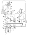
Fig. 1 is a circuit diagram showing a configuration of a switching power supply unit according to an embodiment of the invention; -
Fig. 2 is a circuit diagram for illustrating an example of energy transfer paths in the switching power supply unit; -
Figs. 3A to 3F are timing waveform diagrams for illustrating an example of conversion operation of a DC input voltage; -
Figs. 4A to 4F are timing waveform diagrams for illustrating an example of generation operation of an AC output voltage; -
Figs. 5A and 5B are equivalent circuit diagrams for illustrating operation of a switching circuit in generation operation of the AC output voltage as shown inFig. 4 ; -
Fig. 6 is a circuit diagram for illustrating another example of energy transfer paths in the switching power supply unit; -
Figs. 7A to 7F are timing waveform diagrams for illustrating conversion operation of an AC input voltage; -
Figs. 8A and 8B are equivalent circuit diagrams for illustrating operation of a switching circuit in conversion operation of the AC input voltage as shown inFig. 7 ; -
Figs. 9A to 9F are timing waveform diagrams for illustrating an example of generation operation of a DC output voltage; and -
Fig. 10 is a circuit diagram showing a configuration of a switching power supply unit according to a modification of the invention. - Hereinafter, the best mode for carrying out an embodiment of the invention (hereinafter, simply called embodiment) will be described in detail with reference to drawings.
-
Fig. 1 shows a circuit configuration of a switching power supply unit according to an embodiment of the invention. The switching power supply unit is applied to, for example, a car and the like, and has atransformer 2; a capacitor C1 and abidirectional switching circuit 11 which are provided between thetransformer 2 and amain battery 10 described later;bidirectional switching circuits smoothing circuit 43, and avoltage detection section 44, those being provided between thetransformer 2 and AC voltage input/output terminals T5 and T6 described later; and arectifier circuit 31, asmoothing circuit 32, and avoltage detection section 33, those being provided between thetransformer 2 and anaccessory battery 30; and SW (switching)control circuits - The capacitor C1 is disposed between a high voltage line LH1 and a low voltage line LL1, and acts as a smoothing capacitor. One end of the high voltage line LH1 is connected to an input/output terminal T1, one end of the low voltage line LL1 is connected to an input/output terminal T2, and a
main battery 10 is disposed between the input/output terminals T1 and T2. Themain battery 10 supplies a DC input voltage Vdcin between the input/output terminals T1 and T2, and for example, when the switching power supply unit is applied to a car, the unit is connected to a driving inverter or a step-up/step-down converter, and acts as a high voltage battery of, for example, about 350 to 500 V. - The
switching circuit 11 is a switching circuit in a full-bridge type having four switching elements Q1 to Q4 and four diodes D1 to D4. Specifically, one end of the switching element Q1 is connected to the high voltage line LH1, and the other end thereof is connected to one end of the switching element Q2 and one end of awinding 21 of thetransformer 2 described later. One end of the switching element Q3 is connected to the high voltage line LH1, and the other end thereof is connected to one end of the switching element Q4 and the other end of the winding 21 of thetransformer 2. The other end of the switching element Q2 and the other end of the switching element Q4 are connected to the low voltage line LL1 respectively. The diodes D1 to D4 are connected in parallel in an opposite direction to one another between respective two ends of the switching elements Q1 to Q4 (a cathode of each diode is connected to a side of the high voltage line LH1, and an anode of each diode is connected to a side of the low voltage line LL1). That is, one switching element and one diode configure one bidirectional switch, and thereby the switchingcircuit 11 acts as a bidirectional switching circuit. Specifically, while described later in detail, the switchingcircuit 11 acts as a DC/AC inverter circuit performing DC/AC conversion (conversion from DC to AC) or as a rectifier circuit. Each of the switching elements Q1 to Q4 is configured of, for example, a bipolar transistor, IGBT (Insulated Gate Bipolar Transistor), or MOS-FET (Metal Oxide Semiconductor-Field Effect Transistor). When each of the switching elements Q1 to Q4 is configured of MOS-FET and therefore has a parasitic diode component, such a parasitic diode component may be used in place of each of the diodes D1 to D4. - The
SW control circuit 12 generates switching control signals S1 to S4 based on a DC output voltage Vdcout2 at anaccessory battery 30 side, the voltage Vdcout2 being detected by thevoltage detection section 33 described later, and controls switching operation of each of the switching elements Q1 to Q4 in the switchingcircuit 11 using the generated signals. Specifically, while described later in detail, the switchingcircuit 11 is controlled by theSW control circuit 12 so as to perform the DC/AC conversion operation or the rectification operation as described before. - The
transformer 2 has a winding 21 provided at themain battery 10 side, a winding 22 provided at a side of input/output terminals T5 and T6 described later, and windings 23 (including a pair ofwindings accessory battery 30 side, andrespective windings 21 to 23 are magnetically coupled to one another so as to have the same polarity. The winding 21 is disposed between the other end of the switching element Q1 and one end of the switching element Q4. Both ends of the winding 22 are connected to the switchingcircuit 41 described later, and respective two ends of thewindings rectifier circuit 31. - The switching
circuit 41 is a switching circuit in a full-bridge type having four switching elements Q5 to Q8 and four diodes D5 to D8. Specifically, one end of the switching element Q5 is connected to a high voltage line LH4, and the other end thereof is connected to one end of the switching element Q8 and one end of the winding 22 of thetransformer 2. One end of the switching element Q7 is connected to the high voltage line LH4, and the other end thereof is connected to one end of the switching element Q8 and the other end of the winding 22. The other end of the switching element Q6 and the other end of the switching element Q8 are connected to a low voltage line LL4 respectively. The diodes D5 to D8 are connected in parallel in an opposite direction to one another between respective two ends of the switching elements Q5 to Q8 (a cathode of each diode is connected to a side of the high voltage line LH4, and an anode of each diode is connected to a side of the low voltage line LL4). That is, one switching element and one diode configure one bidirectional switch, and thereby the switchingcircuit 41 also acts as a bidirectional switching circuit. Specifically, while described later in detail, the switchingcircuit 41 acts as a rectifier circuit or a DC/AC inverter circuit. Each of the switching elements Q5 to Q8 is also configured of, for example, a bipolar transistor, IGBT, or MOS-FET. When each of the switching elements Q5 to Q8 is configured of MOS-FET and therefore has a parasitic diode component, such a parasitic diode component may be used in place of each of the diodes D5 to D8. - The
SW control circuit 46 generates switching control signals S5 to S8 based on a DC output voltage Vdcout2 at theaccessory battery 30 side, the voltage Vdcout2 being detected by thevoltage detection section 33 described later, and controls switching operation of each of the switching elements Q5 to Q8 in the switchingcircuit 41 using the generated signals. Specifically, while described later in detail, the switchingcircuit 41 is controlled by theSW control circuit 46 so as to perform the rectification operation or the DC/AC conversion operation as described before. - The capacitor C3 is disposed between the high voltage line LH4 and the low voltage line LL4 in a position between the switching
circuit 41 and aswitching circuit 42 described later, and acts as a smoothing capacitor. - The switching
circuit 42 is a switching circuit in a full-bridge type having four switching elements Q10 to Q13 and four diodes D10 to D13. Specifically, one end of the switching element Q10 is connected to the high voltage line LH4, and the other end thereof is connected to one end of the switching element Q11 and one end of an inductor 43L1 in a smoothingcircuit 43 described later. One end of the switching element Q12 is connected to the high voltage line LH4, and the other end thereof is connected to one end of the switching element Q13 and one end of an inductor 43L2 in the smoothingcircuit 43 described later. The other end of the switching element Q11 and the other end of the switching element Q13 are connected to the low voltage line LL4 respectively. The diodes D10 to D13 are connected in parallel in an opposite direction to one another between respective two ends of the switching elements Q10 to Q13 (a cathode of each diode is connected to a side of the high voltage line LH4, and an anode of each diode is connected to a side of the low voltage line LL4). That is, one switching element and one diode configure one bidirectional switch, and thereby the switchingcircuit 42 also acts as a bidirectional switching circuit. Specifically, while described later in detail, the switchingcircuit 42 acts as a DC/AC inverter circuit or an AC/DC converter circuit performing AC/DC conversion (conversion from AC to DC) . Each of the switching elements Q10 to Q13 is also configured of, for example, a bipolar transistor, IGBT, or MOS-FET. When each of the switching elements Q10 to Q13 is configured of MOS-FET and therefore has a parasitic diode component, such a parasitic diode component may be used in place of each of the diodes D10 to D13. - When the switching
circuit 42 acts as the AC/DC converter circuit, thecircuit 42 acts even as a PFC (Power Factor Correction) circuit performing operation of power factor correction. Specifically, while described later in detail, an input voltage into the switchingcircuit 42 as a PFC circuit can be stepped up and stabilized so as to improve power factor. - The
SW control circuit 45 generates switching control signals S10 to S13 based on an AC output voltage Vacout between the input/output terminals T5 and T6, the voltage Vacout being detected by thevoltage detection section 44 described later, and controls switching operation of each of the switching elements Q10 to Q13 in the switchingcircuit 42 using the generated signals. Specifically, while described later in detail, the switchingcircuit 42 is controlled by theSW control circuit 45 so as to perform the DC/AC conversion operation, AC/DC conversion operation, and PFC operation as described before. - The smoothing
circuit 43 has the two inductors 43L1, 43L2 and acapacitor 43C. The inductor 43L1 is disposed on the connection line L41 in an insertional manner, and one end of the inductor 43L1 is connected to the other end of the switching element Q10 and one end of the switching element Q11, and the other end thereof is connected to the input/output terminal T5 via thevoltage detection section 44. The inductor 43L2 is disposed on the connection line L42 in an insertional manner, and one end of the inductor 43L2 is connected to the other end of the switching element Q12 and one end of the switching element Q13, and the other end of the inductor 43L2 is connected to the input/output terminal T6 via thevoltage detection section 44. Thecapacitor 43C is disposed between the connection line L41 (a portion near the other end of the inductor 43L1) and the connection line L42 (a portion near the other end of the inductor 43L2). - The
voltage detection section 44 detects an AC voltage between the input/output terminal T5 and T6 (specifically, AC output voltage Vacout), and outputs a voltage corresponding to the detected AC output voltage Vacout to theSW control circuit 45. As a specific circuit configuration of thevoltage detection section 44, for example, a circuit configuration is given, in which a voltage dividing resistance (not shown) disposed between the connection line L41 and 0 V potential of theSW control circuit 45, and a voltage dividing resistance disposed between the connection line L42 and 0 V potential of theSW control circuit 45 are used to detect the AC output voltage Vacout and generate the voltage corresponding to the voltage Vacout. - The
rectifier circuit 31 has two diodes 31D1 and 31D2. An anode of the diode 31D1 is connected to one end of the winding 23A. An anode of the diode 31D2 is connected to one end of the winding 23B. Cathodes of the diodes 31D1 and 31D2 are commonly connected to a high voltage line LH3. The other ends of thewindings rectifier circuit 31 is in a cathode common type. - The smoothing
circuit 32 has aninductor 32L and acapacitor 32C. Theinductor 32L is disposed on the high voltage line LH3 in an insertional manner, and one end of the inductor is connected to the cathodes of the diodes 31D1 and 31D2, and the other end thereof is connected to the output terminal T3 via thevoltage detection section 33. Thecapacitor 32C is disposed between the high voltage line LH3 (a portion near the other end of theinductor 32L) and the low voltage line LL3, and the other end of the low voltage line LL3 is connected to the output terminal T4. Theaccessory battery 30 for driving a not-shown accessory (for example, power window) is connected between the output terminals T3 and T4 to supply the DC output voltage Vdcout2 (for example, about 14 V) between the output terminals T3 and T4. - The
voltage detection section 33 detects the DC output voltage Vdcout2 supplied between the output terminals T3 and T4, and outputs a voltage corresponding to the detected DC output voltage Vdcout2 to theSW control circuit 12. As a specific circuit configuration of thevoltage detection section 33, for example, a circuit configuration is given, in which a voltage dividing resistance (not shown) disposed between the high voltage line LH3 and the low voltage line LL3 is used to detect the DC output voltage Vdcout2 and generate a voltage corresponding to the DC output voltage. - The winding 21 corresponds to a specific example of a "first transformer coil" in an embodiment of the invention, the winding 22 corresponds to a specific example of a "second transformer coil" in an embodiment of the invention, and the windings 23 (23A and 23B) correspond to a specific example of a "third transformer coil" in an embodiment of the invention. Moreover, the
main battery 10 corresponds to a specific example of a "first DC power supply" in an embodiment of the invention, and theaccessory battery 30 corresponds to a specific example of a "second DC power supply" in an embodiment of the invention. Moreover, the switchingcircuit 11 corresponds to a specific example of a "first switching circuit" in an embodiment of the invention, the switchingcircuit 41 corresponds to a specific example of a "second switching circuit" in an embodiment of the invention, and the switchingcircuit 42 corresponds to a specific example of a "third switching circuit" in an embodiment of the invention. Therectifier circuit 31 corresponds to a specific example of a "rectifier circuit" in an embodiment of the invention. TheSW control circuits - Next, operation of the switching power supply unit having a configuration as above is described in detail.
- First, with reference to
Figs. 1 to 5A and5B , detailed description is made on operation in the case that when the DC input voltage Vdcin is supplied from themain battery 10, the AC output voltage Vacout is outputted from the input/output terminals T5 and T6. For example, when the DC input voltage Vdcin is supplied from themain battery 10 in this way, in the case that the switching power supply unit of the embodiment is applied to a car, the operation corresponds to operation in the case that a power is supplied from a motor driving inverter or a step-up/step-down converter to themain battery 10, thereby theaccessory battery 30 drives an accessory and outputs the AC output voltage Vacout to the outside, that is, the relevant operation corresponds to operation during engine operation (car running), or operation in the case that the AC output voltage Vacout is outputted based on only the DC input voltage Vdcin supplied from themain battery 10 during engine stopping. For example, the commercial power voltage may be supposed as the Vacout. -
Fig. 2 schematically shows an example of energy transfer paths when the DC input voltage Vdcin is supplied from themain battery 10 usingarrows energy transfer path 61 in theenergy transfer paths - First, operation of generation and output of the DC output voltage Vdcout2 at the
accessory battery 30 side is described in detail with reference toFigs. 1 and2 . - When a DC input voltage Vdcin is inputted from the
main battery 10 via the input/output terminals T1 and T2, the switchingcircuit 11 acts as a DC/AC inverter circuit, and switches the DC input voltage Vdcin, so that an AC pulse voltage is generated and supplied to the winding 21 of thetransformer 2. Thus, a transformed (here, stepped-down) AC pulse voltage is generated at thewindings transformer 2. In this case, a transformation level is determined by a winding ratio of the winding 21 to thewindings - Next, the transformed AC pulse voltage is rectified by the diodes 31D1 and 31D2 in the
rectifier circuit 31. Thus, rectified output is produced between the high voltage line LH3 and the low voltage line LL3. - Next, the smoothing
circuit 32 smoothes the rectified output produced between the high voltage line LH3 and the low voltage line LL3, and the DC output voltage Vdcout2 is thus outputted from the output terminals T3 and T4. The DC output voltage Vdcout2 is supplied to theaccessory battery 30, and used to drive a not-shown accessory. The DC output voltage Vdcout2 is detected by thevoltage detection section 33, and switching control signals S1 to S4 are outputted form theSW control circuit 12 to the switchingcircuit 11 based on the detected DC output voltage Vdcout2, thereby the switchingcircuit 11 performs DC/AC conversion operation, and the switching elements Q1 to Q4 in the switchingcircuit 11 are subjected to PWM (Pulse Width Modulation) control such that the DC output voltage Vdcout is constant. - In this way, the DC input voltage Vdcin supplied from the
main battery 10 is subjected to DC voltage conversion into the DC output voltage Vdcout2,by the switchingcircuit 11,windings transformer 2,rectifier circuit 31, and smoothingcircuit 32, those collectively acting as the DC/DC converter, and then the DC output voltage is outputted from the output terminals T3 and T4. Thus, theaccessory battery 30 is subjected to constant-voltage charge, and a not-shown accessory is driven. - Next, operation of generation and output of the AC output voltage Vacout is described in detail with reference to
Figs. 1 to 5A and5B . Theenergy transfer path 62 shown inFig. 2 corresponds to the operation of generation and output of the AC output voltage Vacout (operation as the DC/AC inverter). -
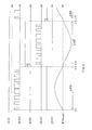
Figs. 3A to 3F show, by timing waveform diagrams, an example of operation of performing voltage conversion and rectification of the DC input voltage Vdcin; whereinFig. 3A shows switching control signals S1 and S4,Fig. 3B shows switching control signals S2 and S3,Fig. 3C shows a voltage V22 generated between both ends of the winding 22 of thetransformer 2,Fig. 3D shows switching control signals S5 and S8,Fig. 3E shows switching control signals S6 and S7, andFig. 7F shows a voltage V3 between both ends of the capacitor C3.Figs. 4A to 4F show, by timing waveform diagrams, an example of operation of generation and output of the AC output voltage Vacout based on the voltage V3; whereinFig. 4A shows a voltage V3 between both ends of the capacitor C3,Figs. 4B to 4E show switching control signals S10 to S13 respectively, andFig. 4F shows the AC output voltage Vacout. Each of directions of arrows shown inFig. 2 shows each of positive directions of the voltages V22, V3 and Vacout. - First, when the DC input voltage Vdcin is inputted from the
main battery 10 via the input/output terminals T1 and T2, as shown in a period of timing t1 to timing t8 inFig. 3 , an AC pulse voltage is generated by the switchingcircuit 11 based on the switching control signals S1 to S4 (Figs. 3A and 3B ), and the AC pulse voltage is supplied to the winding 21 of thetransformer 2. At that time, a transformedAC pulse voltage 22 is generated at thewindings transformer 2, in addition, generated at the winding 22 thereof (Fig. 3C ). Even in this case, a transformation level is determined by the winding ratio of the winding 21 to the winding 22. - Next, the transformed AC pulse voltage is rectified by the diodes D5 to D8 in the switching
circuit 41 acting as the rectifier circuit. Thus, for example, rectified output (voltage V3) as shown inFig. 3F andFig. 4A is produced between the high voltage line LH4 and the low voltage line LL4 (between both ends of the capacitor C3). The respective switching elements Q5 to Q8 perform PWM operation according to the switching control signals S5 to S8 (Figs. 3D and 3E ), and the switchingcircuit 41 performs synchronous rectification operation in order to reduce switching loss in the respective switching elements Q5 to Q8. - Next, the switching
circuit 42 acts as a DC/AC inverter, and the switching elements Q10 to Q13 switch the voltage V3 according to the switching control signals S10 to S13 (seeFigs. 4B to 4E ) from theSW control circuit 45. - Specifically, for example, first, in a period of timing t11 to timing t12 (positive half-wave period Δ62A), the switching control signal S13 normally shows "H" (
Fig. 4E ) and thus the switching element Q13 is in a normally on state, and the switching control signal S12 normally shows "L" (Fig. 4D ) and thus the switching element Q12 is in a normally off state. Thus, an equivalent circuit of a section including the switchingcircuit 42 and the smoothingcircuit 43 is given as shown inFig. 5A . In this period, as shown inFig. 4B , the switching control signal S10 is gradually increased in pulse width in the first half of the period of timing t11 to timing t12, and gradually decreased in pulse width in the second half of the period of timing t11 to timing t12. Moreover, the switching control signal S11 normally shows "L" as shown inFig. 4C . That is, in the period, the switching element Q11 is in a normally off state and thus the diode D11 becomes conductive, and the switching element Q10 is in an on/off state according to PWM control. Therefore, in the positive half-wave period Δ62A, along theenergy path 62A shown inFig. 5A , the AC output voltage Vacout outputted from the input/output terminals T5 and T6 has a sine waveform being convex upward as shown inFig. 4F due to the switching operation by the switching elements Q10 to Q13 and smoothing processing by the smoothingcircuit 43. In the positive half-wave period Δ62A, the switching element Q11 may be in the normally on state to achieve synchronous rectification operation. In such a case, switching loss in the switching element Q11 is preferably reduced. - A subsequent period of timing t12 to timing t13 corresponds to dead time Td in which all of the switching elements Q10 to Q13 are in the off state (
Figs. 4B to 4E ). - Next, in a period of timing t13 to timing t14 (negative half-wave period Δ62B), the switching control signal S11 normally shows "H" (
Fig. 4C ) and thus the switching element Q11 is in a normally on state, and the switching control signal S10 normally shows "L" (Fig. 4B ) and thus the switching element Q10 is in a normally off state. Thus, as shown inFig. 5B , an equivalent circuit of a section including the switchingcircuit 42 and the smoothingcircuit 43 is in a configuration vertically opposite to that in a portion of the smoothingcircuit 43 as shown inFig. 5A . In this period, as shown inFig. 4D , the switching control signal S12 is gradually increased in pulse width in the first half of the period of timing t13 to timing t14, and gradually decreased in pulse width in the second half of the period of timing t13 to timing t14. Moreover, the switching control signal S13 normally shows "L" as shown inFig. 4E . That is, in the period, the switching element Q13 is in a normally off state and thus the diode D13 becomes conductive, and the switching element Q12 is in an on/off state according to PWM control. Therefore, in the negative half-wave period Δ62B, along theenergy path 62B shown inFig. 5B , the AC output voltage Vacout outputted from the input/output terminals T5 and T6 has a sine waveform being convex downward as shown inFig. 4F due to the switching operation by the switching elements Q10 to Q13 and smoothing processing by the smoothingcircuit 43. Even in the negative half-wave period Δ62B, the switching element Q13 may be in the normally on state to achieve synchronous rectification operation. In such a case, switching loss in the switching element Q13 is preferably reduced. - A subsequent period of timing t14 to timing t15 also corresponds to the dead time Td in which all of the switching elements Q10 to Q13 are in the off state (
Figs. 4B to 4E ). An operation condition at timing t15 is equivalent to an operation condition at timing t11. After the timing t15, operation in the period of timing t11 to timing t15 is repeated. The AC output voltage Vacout outputted from the output terminals T5 and T6 is detected by thevoltage detection section 44, and the switching control signals S10 to S13 are outputted from theSW control circuit 45 to the switchingcircuit 42 based on the detected AC output voltage Vacout, thereby the switching elements Q10 to Q13 in the switchingcircuit 42 are controlled in pulse width such that the switchingcircuit 42 performs DC/AC conversion operation, and the AC output voltage Vacout is stabilized. When the AC output voltage Vacout is supplied between the output terminals T5 and T6, the voltage Vacout acts as a power voltage of electric devices, that is, acts as a so-called commercial power voltage. - In this way, when the DC input voltage Vdcin is supplied from the
main battery 10 as shown inFig. 2 , based on the DC input voltage Vdcin inputted from themain battery 10, the DC output voltage Vdcout2 is generated by the DC/DC converter including the switchingcircuit 11,SW control circuit 12,windings transformer 2,rectifier circuit 31, and smoothingcircuit 33, and is outputted from the output terminals T3 and T4, and the AC output voltage Vacout is generated by the DC/AC inverter including the switchingcircuit 11,windings transformer 2, switchingcircuit 41, switchingcircuit 42,SW control circuits circuit 43, and is outputted from the output terminals T5 and T6. - Next, with reference to
Fig. 1 andFigs. 6 to 9A to 9F , detailed description is made on operation in the case that the AC input voltage Vacin is inputted from the input/output terminals T5 and T6 (operation in the case that DC output voltages Vdcout1 and Vdcout2 are generated based on the AC input voltage Vacin and outputted to themain battery 10 and theaccessory battery 30 to charge the batteries respectively). In operation in this case, for example, in the case that the switching power supply unit of the embodiment is applied to a car, when an engine is stopped, the AC input voltage Vacin is inputted from an external commercial power supply 50 in order to charge at least one of themain battery 10 and theaccessory battery 30. -
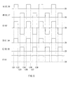
Fig. 6 schematically shows an example of energy transfer paths byarrows Figs. 7A to 7F andFigs. 9A to 9F show operation waveforms in such a case by timing waveform diagrams respectively. Specifically,Figs. 7A to 7f show operation waveforms before the voltage V3 between both ends of the capacitor C3 is generated based on the AC input voltage Vacin; whereinFig. 7A shows the AC input voltage Vacin,Figs. 7B to 7E show switching control signals S10 to S13 respectively, andFig. 7F shows the voltage V3 between both ends of the capacitor C3, respectively.Figs. 9A to 9F show operation waveforms before the capacitor C1 is charged (themain battery 10 is charged) based on the voltage V3; whereinFig. 9A shows switching control signals S5 and S8,Fig. 9B shows switching control signals S6 and S7,Fig. 9C shows a voltage V21 generated between both ends of the winding 21 of thetransformer 2,Fig. 9D shows switching control signals S1 and S4,Fig. 9E shows switching control signals S2 and S3, andFig. 9F shows the voltage V1 between both ends of the capacitor C1, respectively. Directions of arrows shown inFig. 6 show positive directions of the AC input voltage Vacin, and the voltages V3, V21 and V1 respectively. - When an AC input voltage Vacin (commercial power voltage) as shown in
Fig. 7A is inputted from the commercial power supply 50 via the input/output terminals T5 and T6, the AC input voltage is subjected to smoothing processing for removing noise components by the smoothingcircuit 43, and then inputted into the switchingcircuit 42. Then, the switchingcircuit 42 acts as a step-up AC/DC converter using inductor components of the inductors 43L1 and 43L2, and the switching elements Q10 to Q13 switch the AC input voltage Vacin according to the switching control signals S10 to S13 (Figs. 7B to 7E ) from theSW control circuit 45 respectively. TheSW control circuit 45 is controlled based on an output voltage from the switchingcircuit 42. - Specifically, for example, first, in a period of timing t21 to timing t22 (positive half-wave period Δ63A (Δ64A) in which the AC input voltage Vacin has a sine waveform being convex upward), the switching control signal S13 normally shows "H" (
Fig. 7E ) and thus the switching element Q13 is in a normally on state, and the switching control signal S12 normally shows "L" (Fig. 7D ) and thus the switching element Q12 is in a normally off state. Thus, an equivalent circuit of a section including the switchingcircuit 42 and the smoothingcircuit 43 is given as shown inFig. 8A . In this period, as shown inFig. 7C , the switching control signal S11 is gradually decreased in pulse width in the first half of the period of timing t21 to timing t22, and gradually increased in pulse width in the second half of the period of timing t21 to timing t22. Moreover, the switching control signal S10 normally shows "L" as shown inFig. 7B . That is, in the period, the switching element Q10 is in a normally off state and thus the diode D12 becomes conductive, and the switching element Q11 is in an on/off state according to PWM control. Therefore, in the positive half-wave period Δ63A (Δ64A), along theenergy paths Fig. 8A , the voltage V3 between both ends of the capacitor C3 becomes a DC voltage having a constant value as shown inFig. 7F due to smoothing processing by the smoothingcircuit 43 and the switching operation by the switching elements Q10 to Q13. In the positive half-wave period Δ63A (Δ64A), the switching element Q10 may be in an opposite-phase state with respect to the switching element Q11 to achieve synchronous rectification operation. In such a case, switching loss and conduction loss in the diode D10 are preferably reduced. - Next, in a period of timing t22 to timing t23 (negative half-wave period Δ63B (Δ64B) in which the AC input voltage Vacin has a sine waveform being convex downward), the switching control signal S11 normally shows "H" (
Fig. 7C ) and thus the switching element Q11 is in a normally on state, and the switching control signal S10 normally shows "L" (Fig. 7B ) and thus the switching element Q10 is in a normally off state. Thus, as shown inFig. 8B , an equivalent circuit of a section including the switchingcircuit 42 and the smoothingcircuit 43 is in a configuration vertically opposite to that shown inFig. 8A in the portion of the smoothingcircuit 43. In this period, the switching control signal S11 is gradually decreased in pulse width in the first half of the period of timing t22 to timing t23, and gradually increased in pulse width in the second half of the period of timing t22 to timing t23 as shown inFig. 7E . Moreover, the switching control signal S12 normally shows "L" as shown inFig. 7D . That is, in the period, the switching element Q12 is in a normally off state and thus the diode D12 becomes conductive, and the switching element Q13 is in an on/off state according to PWM control. Therefore, in the negative half-wave period Δ63B (Δ64B), along theenergy paths Fig. 8B , the voltage V3 between both ends of the capacitor C3 becomes a DC voltage having a constant value as shown inFig. 7F due to smoothing processing by the smoothingcircuit 43 and the switching operation by the switching elements Q10 to Q13. Even in the negative half-wave period A63B (Δ64B), the switching element Q12 may be in an opposite-phase state with respect to the switching element Q13 to achieve synchronous rectification operation. In such a case, switching loss and conduction loss in the diode D12 are preferably reduced. - In the switching
circuit 42 and the smoothingcircuit 43, power factor is improved compared with a rectifier in a capacitor input type for performing the AC/DC conversion operation. Thus, a peak current is reduced, and thereby a ripple voltage is reduced compared with a smoothing capacitor having the same capacity. - Next, the
main battery 10 and theaccessory battery 30 are charged through theenergy transfer paths - First, along the
energy transfer path 63, the switchingcircuit 41 acts as the DC/AC inverter circuit, and the switching elements Q5 to Q8 perform on/off operation as shown in a period of timing t31 to timing t38 inFigs. 9A and 9B and the like, thereby an AC pulse voltage is generated at the winding 22 of thetransformer 2. Then, a transformedAC pulse voltage 21 as shown inFig. 9C is generated between both ends of the winding 21 depending on a winding ratio of the winding 22 to the winding 21. Next, the switchingcircuit 11 acts as a rectifier circuit in this case, and the switching elements Q1 to Q4 perform on/off operation as shown inFigs. 9D and 9E , thereby theAC pulse voltage 21 is rectified, and a constant DC voltage V1 as shown inFig. 9F is applied between both ends of the capacitor C1. In this way, themain battery 10 is charged by the DC output voltage Vdcout1 based on the voltage V1. The switching elements Q1 to Q4 perform PWM operation according to the switching control signals S1 to S4 respectively, the PWM operation being synchronized with PWM operation of the switchingcircuit 41. - On the other hand, along the
energy transfer path 64, when the AC pulse voltage is generated at the winding 22 of thetransformer 2 as above, a transformed AC pulse voltage is generated even at thewindings transformer 2, a transformation level of the transformed voltage being determined by a winding ratio of the winding 22 to thewindings rectifier circuit 31, and then smoothed by the smoothingcircuit 32, thereby theaccessory battery 30 is also charged by a constant voltage (DC output voltage Vdcout2) . The DC output voltage Vdcout2 is detected by thevoltage detection section 33, and the switching control signals S10 to S13 are outputted from theSW control circuit 45 to the switchingcircuit 42 based on the detected DC output voltage Vdcout2, thereby the switchingcircuit 42 performs AC/DC conversion operation, and the switching elements Q10 to Q13 in the switchingcircuit 42 are subjected to PWM control such that the voltage V3 between both ends of the capacitor C3 is constant. Similarly, the switching control signals S5 to S8 are outputted from theSW control circuit 46 to the switchingcircuit 41 based on the detected DC output voltage Vdcout2, thereby the switchingcircuit 41 performs DC/AC conversion operation, and the switching elements Q5 to Q8 in the switchingcircuit 41 are subjected to PWM control such that each of the DC output voltages Vdcout1 and Vdcout2 is constant. - In this way, when the AC input voltage Vacin (commercial power voltage) is supplied from the commercial power supply 50 as shown in
Fig. 6 , based on the inputted AC input voltage Vacin, the DC output voltage Vdcout1 is generated by the smoothingcircuit 43, switchingcircuit 42,SW control circuit 45, switchingcircuit 41,SW control circuit 46,windings transformer 2, switchingcircuit 11, andSW control circuit 12, and is outputted from the input/output terminals T1 and T2, and the DC output voltage Vdcout2 is generated by the smoothingcircuit 43, switchingcircuit 42,SW control circuit 45, switchingcircuit 41,SW control circuit 46,windings transformer 2,rectifier circuit 31, and smoothingcircuit 32, and is outputted from the output terminals T3 and T4. Thus, at least one of themain battery 10 and theaccessory battery 30 is charged. - As hereinbefore, in the embodiment, the switching
circuit 11 is provided between the winding 21 of thetransformer 2 and themain battery 10, the switchingcircuit 41 is provided between the winding 22 of thetransformer 2 and the input/output terminals T5 and T6, and the switchingcircuit 42 is provided between the switchingcircuit 41 and the input/output terminals T5 and T6, and each of the switchingcircuits main battery 10 to charge thebattery 10. Accordingly, input terminals of an AC voltage can be made common to output terminals of an AC voltage by the input/output terminals T5 and T6. - Moreover, the
transformer 2 has thewindings windings rectifier circuit 31 is further provided between thewindings accessory battery 30. Therefore, based on the DC input voltage Vdcin from themain battery 10, DC voltage conversion (DC/DC converter) operation to theaccessory battery 30 can be performed in addition to DC/AC conversion (DC/AC inverter) operation to the input/output terminals T5 and T6. In addition, charging operation can be performed to at least one of themain battery 10 and theaccessory battery 30 by the DC output voltages Vdcout1 and Vdcout2 based on the AC input voltage Vacin from the input/output terminals T5 and T6. - While the invention has been described with the embodiment hereinbefore, the invention is not limited to the embodiment, and can be variously altered or modified.
- For example, while description was made in the embodiment on the case that each of the switching
circuits circuits - Moreover, description was made in the embodiment on a case that the
transformer 2 had thewindings rectifier circuit 31, smoothingcircuit 32, andvoltage detection section 33 were provided at the winding 23 side, thereby operation of generation and output of the DC output voltage Vdcout2 (operation as the DC/DC converter) based on the DC input voltage Vdcin was performed in addition to output operation of the AC output voltage Vacout (operation as the DC/AC inverter) and input operation of the AC input voltage Vacin (operation as the AC/DC converter). However, for example, when theaccessory battery 30 is unnecessary and therefore operation as the DC/DC converter is also unnecessary, for example, as the switching power supply unit shown inFig. 10 , atransformer 2A having only thewindings transformer 2, and therectifier circuit 31, smoothingcircuit 32, andvoltage detection section 33 at a winding 23 side may not be provided. - Furthermore, description was made in the embodiment on a case that the switching
circuit 41 performed PWM operation and the switchingcircuit 11 performed rectification in synchronization with the switchingcircuit 41, for example, as shown inFig. 3 orFig. 9 . However, for example, when the DC output voltage Vdcout1 is generated based on the AC input voltage Vacin, and is outputted into themain battery 10 to charge thebattery 10, while the switching elements Q5 to Q8 in the switchingcircuit 41 perform switching operation with a variable pulse width respectively, the switching elements Q1 to Q4 in the switchingcircuit 11 perform switching operation with a fixed pulse width respectively, so that a charge level of themain battery 10 can be adjusted. - Obviously, many modifications and variations of the present invention are possible in the light of the above teachings. It is therefore to be understood that within the scope of the appended claims the invention may be practiced otherwise than as specifically described.
Claims (4)
- A switching power supply unit, comprising:a transformer including a first transformer coil and a second transformer coil magnetically coupled to each other,a first bidirectional switching circuit disposed between the first transformer coil and a first DC power supply, and configured to include at least one switch array configured of a pair of switches connected in series,a second bidirectional switching circuit disposed between the second transformer coil and AC voltage input/output terminals, and configured such that switch arrays are connected in parallel to each other, each of the switch arrays being configured of a pair of switches connected in series,a third bidirectional switching circuit disposed between the second switching circuit and the AC voltage input/output terminals, and configured to include at least one switch array configured of a pair of switches connected in series, anda control section controlling the first to third switching circuits.
- The switching power supply unit according to claim 1:wherein the control section controls the switching circuits such that;in output mode where an AC output voltage is outputted from the AC voltage input/output terminals based on a DC input voltage supplied from the first DC power supply, the first and third switching circuits perform DC/AC conversion respectively, and the second switching circuit performs rectification; andin input mode where a DC output voltage is supplied into the first DC power supply based on an AC input voltage inputted from the AC voltage input/output terminals, the third switching circuit performs AC/DC conversion, the second switching circuit performs DC/AC conversion, and the first switching circuit performs rectification.
- The switching power supply unit according to claim 2 :wherein the control section controls the switching circuits such that the third switching circuit further performs power-factor improvement in the input mode.
- The switching power supply unit according to claim 1 :the transformer has a third transformer coil magnetically coupled to the first transformer coil and the second transformer coil, anda rectifier circuit is further provided between the third transformer coil and a second DC power supply.
Applications Claiming Priority (1)
| Application Number | Priority Date | Filing Date | Title |
|---|---|---|---|
| JP2007039551A JP4400632B2 (en) | 2007-02-20 | 2007-02-20 | Switching power supply |
Publications (2)
| Publication Number | Publication Date |
|---|---|
| EP1962415A2 true EP1962415A2 (en) | 2008-08-27 |
| EP1962415A3 EP1962415A3 (en) | 2014-07-09 |
Family
ID=39415047
Family Applications (1)
| Application Number | Title | Priority Date | Filing Date |
|---|---|---|---|
| EP08002953.1A Withdrawn EP1962415A3 (en) | 2007-02-20 | 2008-02-18 | Switching power supply unit |
Country Status (3)
| Country | Link |
|---|---|
| US (1) | US7764527B2 (en) |
| EP (1) | EP1962415A3 (en) |
| JP (1) | JP4400632B2 (en) |
Cited By (14)
| Publication number | Priority date | Publication date | Assignee | Title |
|---|---|---|---|---|
| EP2434604A1 (en) * | 2010-09-22 | 2012-03-28 | Kabushiki Kaisha Toyota Jidoshokki | Power source device |
| WO2012060958A2 (en) * | 2010-11-05 | 2012-05-10 | American Power Conversion Corporation | System and method for bidirectional dc-ac power conversion |
| CN102694409A (en) * | 2011-03-18 | 2012-09-26 | 株式会社万都 | Battery charging apparatus |
| WO2012041613A3 (en) * | 2010-09-27 | 2012-09-27 | Siemens Aktiengesellschaft | A bi-directional dc-dc converter and a system for starting and controlling a power plant |
| CN104471850A (en) * | 2012-07-20 | 2015-03-25 | 智能电子系统公司 | Multi-directional converter comprising three ports and a single transformer for electric vehicles |
| CN104670126A (en) * | 2013-09-26 | 2015-06-03 | 李尔公司 | On-board charger having power supply management with automatic power transition |
| CN105121212A (en) * | 2013-01-31 | 2015-12-02 | 罗伯特·博世有限公司 | Power transmission arrangement |
| CN105226989A (en) * | 2014-06-27 | 2016-01-06 | 联合汽车电子有限公司 | The power electronics integrated system of new-energy automobile and method of work thereof |
| EP2858225A4 (en) * | 2012-05-24 | 2017-03-15 | Mitsubishi Electric Corporation | Power conversion device |
| CN106664023A (en) * | 2014-10-20 | 2017-05-10 | 三菱电机株式会社 | Electric power conversion device |
| CN108173323A (en) * | 2016-12-05 | 2018-06-15 | 飞宏科技股份有限公司 | A kind of two-way vehicle-mounted charge-discharge system and its method |
| WO2019140801A1 (en) * | 2018-01-17 | 2019-07-25 | 深圳威迈斯新能源股份有限公司 | Charging circuit for dual-output port, and control method therefor |
| US10804723B2 (en) | 2018-01-17 | 2020-10-13 | Shenzhen Vmax Power Co., Ltd. | Dual-output port charging circuit and control method |
| CN113394979A (en) * | 2020-03-12 | 2021-09-14 | Oppo广东移动通信有限公司 | Power supply device and charging control method |
Families Citing this family (53)
| Publication number | Priority date | Publication date | Assignee | Title |
|---|---|---|---|---|
| JP4320336B2 (en) * | 2006-10-24 | 2009-08-26 | Tdk株式会社 | Switching power supply |
| US8274804B2 (en) * | 2008-03-04 | 2012-09-25 | Mitsubishi Electric Corporation | Voltage transforming apparatus |
| TWI386789B (en) * | 2008-12-29 | 2013-02-21 | Acbel Polytech Inc | Three port type AC and DC power supply |
| US20100244773A1 (en) * | 2009-03-27 | 2010-09-30 | Gm Global Technology Operations, Inc. | Unity power factor isolated single phase matrix converter battery charger |
| US8466658B2 (en) * | 2009-08-05 | 2013-06-18 | GM Global Technology Operations LLC | Systems and methods for bi-directional energy delivery with galvanic isolation |
| US8350523B2 (en) * | 2009-08-05 | 2013-01-08 | GM Global Technology Operations LLC | Charging system with galvanic isolation and multiple operating modes |
| US20110095808A1 (en) * | 2009-10-19 | 2011-04-28 | Colin Reason | System and Method for Controlling Powered Device With Detachable, Controllable Switching Device |
| DE102009046422A1 (en) * | 2009-11-05 | 2011-05-12 | Daniel Schneider | Charging system for electric vehicles |
| US8288887B2 (en) * | 2009-11-19 | 2012-10-16 | GM Global Technology Operations LLC | Systems and methods for commutating inductor current using a matrix converter |
| FR2956529B1 (en) * | 2010-02-17 | 2012-03-16 | Inst Polytechnique Grenoble | MAGNETIC COUPLING BALANCING SYSTEM OF A SERIES ASSOCIATION OF GENERATING OR STORAGE ELEMENTS OF ELECTRICAL ENERGY |
| US8410635B2 (en) * | 2010-03-16 | 2013-04-02 | GM Global Technology Operations LLC | Systems and methods for deactivating a matrix converter |
| JP5632191B2 (en) * | 2010-04-28 | 2014-11-26 | パナソニック株式会社 | Bidirectional DC / DC converter |
| US8462528B2 (en) | 2010-07-19 | 2013-06-11 | GM Global Technology Operations LLC | Systems and methods for reducing transient voltage spikes in matrix converters |
| US8981589B2 (en) * | 2010-08-24 | 2015-03-17 | GM Global Technology Operations LLC | Switched battery and capacitor arrangement and related operating methods |
| US8467197B2 (en) | 2010-11-08 | 2013-06-18 | GM Global Technology Operations LLC | Systems and methods for compensating for electrical converter nonlinearities |
| US8587962B2 (en) | 2010-11-08 | 2013-11-19 | GM Global Technology Operations LLC | Compensation for electrical converter nonlinearities |
| US8599577B2 (en) | 2010-11-08 | 2013-12-03 | GM Global Technology Operations LLC | Systems and methods for reducing harmonic distortion in electrical converters |
| US8614564B2 (en) | 2010-11-18 | 2013-12-24 | GM Global Technology Operations LLS | Systems and methods for providing power to a load based upon a control strategy |
| US8860379B2 (en) | 2011-04-20 | 2014-10-14 | GM Global Technology Operations LLC | Discharging a DC bus capacitor of an electrical converter system |
| US8829858B2 (en) | 2011-05-31 | 2014-09-09 | GM Global Technology Operations LLC | Systems and methods for initializing a charging system |
| JP5691925B2 (en) * | 2011-08-03 | 2015-04-01 | トヨタ自動車株式会社 | CHARGE SYSTEM, VEHICLE MOUNTING THE SAME, AND CHARGING DEVICE CONTROL METHOD |
| DE102011081720A1 (en) * | 2011-08-29 | 2013-02-28 | Robert Bosch Gmbh | Converter circuit and method for transmitting electrical energy |
| US8878495B2 (en) | 2011-08-31 | 2014-11-04 | GM Global Technology Operations LLC | Systems and methods for providing power to a load based upon a control strategy |
| TWI454036B (en) * | 2012-01-09 | 2014-09-21 | Richtek Technology Corp | Bridge rectifier for a pfc power converter |
| KR20140025936A (en) * | 2012-08-23 | 2014-03-05 | 삼성전자주식회사 | Dc/dc converter, electronic apparatus having the same and dc/dc conversion method thereof |
| JP6070263B2 (en) * | 2013-02-26 | 2017-02-01 | 住友電気工業株式会社 | DC-AC converter and control circuit |
| JP6292497B2 (en) * | 2013-03-18 | 2018-03-14 | パナソニックIpマネジメント株式会社 | Power converter, power conditioner |
| US9770991B2 (en) | 2013-05-31 | 2017-09-26 | GM Global Technology Operations LLC | Systems and methods for initializing a charging system |
| US9531300B2 (en) * | 2013-09-16 | 2016-12-27 | Enphase Energy, Inc. | Single phase cycloconverter with integrated line-cycle energy storage |
| CN103546047B (en) * | 2013-10-25 | 2016-04-27 | 矽力杰半导体技术(杭州)有限公司 | A kind of circuit of synchronous rectification and Switching Power Supply being applicable to electronic transformer |
| US10250157B2 (en) | 2013-10-25 | 2019-04-02 | Silergy Semiconductor Technology (Hangzhou) Ltd. | Synchronous rectification circuit and switching power supply thereof |
| JP6140602B2 (en) * | 2013-12-19 | 2017-05-31 | 株式会社Soken | Power converter |
| EP2928038A1 (en) * | 2014-03-31 | 2015-10-07 | ABB Technology AG | Inductive power transfer system and method for operating an inductive power transfer system |
| US9931951B2 (en) | 2014-06-13 | 2018-04-03 | University Of Maryland | Integrated dual-output grid-to-vehicle (G2V) and vehicle-to-grid (V2G) onboard charger for plug-in electric vehicles |
| US10926649B2 (en) * | 2014-12-22 | 2021-02-23 | Flex Power Control, Inc. | Method to reduce losses in a high voltage DC link converter |
| JP6270753B2 (en) * | 2015-02-06 | 2018-01-31 | 三菱電機株式会社 | Power converter |
| JP2016226192A (en) * | 2015-06-01 | 2016-12-28 | 住友電気工業株式会社 | Electric power conversion device |
| CN106904083B (en) * | 2015-12-18 | 2019-09-13 | 比亚迪股份有限公司 | The control method of electric car and its onboard charger and onboard charger |
| GB2556914A (en) * | 2016-11-25 | 2018-06-13 | Dyson Technology Ltd | Battery system |
| CN206559220U (en) * | 2017-03-03 | 2017-10-13 | 上海思致汽车工程技术有限公司 | A kind of portable power TED transferred electron device |
| US20190089262A1 (en) | 2017-09-19 | 2019-03-21 | Texas Instruments Incorporated | Isolated dc-dc converter |
| US10432102B2 (en) | 2017-09-22 | 2019-10-01 | Texas Instruments Incorporated | Isolated phase shifted DC to DC converter with secondary side regulation and sense coil to reconstruct primary phase |
| JP6963487B2 (en) * | 2017-12-14 | 2021-11-10 | シャープ株式会社 | DC / DC converter |
| TWI680631B (en) * | 2018-03-27 | 2019-12-21 | 台達電子工業股份有限公司 | Surge protective apparatus of power conversion circuit |
| SG11202011091QA (en) * | 2018-05-10 | 2020-12-30 | Toshiba Kk | Dc transformation system |
| CN109193918B (en) * | 2018-09-12 | 2022-07-26 | 苏州汇川联合动力系统有限公司 | Backup power supply, driving controller and electric automobile |
| JP7165554B2 (en) * | 2018-10-05 | 2022-11-04 | 株式会社デンソー | power converter |
| JPWO2020189295A1 (en) * | 2019-03-20 | 2020-09-24 | ||
| CN112970182A (en) | 2019-06-28 | 2021-06-15 | 华为技术有限公司 | AC-DC three-level conversion system with high-frequency intermediate AC and two independent outputs |
| CN110774909A (en) * | 2019-09-23 | 2020-02-11 | 华为技术有限公司 | OBC circuit, OBC charger, new energy automobile and fill electric pile |
| JP7275065B2 (en) * | 2020-04-06 | 2023-05-17 | 株式会社Soken | power converter |
| US11594973B2 (en) * | 2020-08-04 | 2023-02-28 | Delta Electronics Inc. | Multiple-port bidirectional converter and control method thereof |
| WO2023140010A1 (en) * | 2022-01-20 | 2023-07-27 | 三菱電機株式会社 | Power source circuit |
Citations (2)
| Publication number | Priority date | Publication date | Assignee | Title |
|---|---|---|---|---|
| JPH08317508A (en) | 1995-05-17 | 1996-11-29 | Nippondenso Co Ltd | Charging device for electric vehicle |
| JP2007039551A (en) | 2005-08-03 | 2007-02-15 | Dainippon Ink & Chem Inc | Epoxy resin, epoxy resin composition, cured product, semiconductor device, and method for producing the epoxy resin |
Family Cites Families (8)
| Publication number | Priority date | Publication date | Assignee | Title |
|---|---|---|---|---|
| US4719550A (en) * | 1986-09-11 | 1988-01-12 | Liebert Corporation | Uninterruptible power supply with energy conversion and enhancement |
| DE3743317A1 (en) | 1987-12-21 | 1989-06-29 | Bosch Gmbh Robert | VEHICLE WIRE NETWORK SYSTEM |
| JP2502421B2 (en) | 1991-08-31 | 1996-05-29 | 積水化成品工業株式会社 | Thermoplastic polyester resin foam sheet having water absorbency and method for producing the same |
| JP3697112B2 (en) | 1999-07-23 | 2005-09-21 | 株式会社千代田 | DC bidirectional converter |
| US6330170B1 (en) * | 1999-08-27 | 2001-12-11 | Virginia Tech Intellectual Properties, Inc. | Soft-switched quasi-single-stage (QSS) bi-directional inverter/charger |
| JP2003153597A (en) | 2001-11-14 | 2003-05-23 | Toyota Motor Corp | Power supply |
| JP4591304B2 (en) * | 2005-10-17 | 2010-12-01 | 株式会社豊田自動織機 | Bidirectional DC / AC inverter |
| JP4320336B2 (en) * | 2006-10-24 | 2009-08-26 | Tdk株式会社 | Switching power supply |
-
2007
- 2007-02-20 JP JP2007039551A patent/JP4400632B2/en not_active Expired - Fee Related
-
2008
- 2008-02-15 US US12/071,134 patent/US7764527B2/en not_active Expired - Fee Related
- 2008-02-18 EP EP08002953.1A patent/EP1962415A3/en not_active Withdrawn
Patent Citations (2)
| Publication number | Priority date | Publication date | Assignee | Title |
|---|---|---|---|---|
| JPH08317508A (en) | 1995-05-17 | 1996-11-29 | Nippondenso Co Ltd | Charging device for electric vehicle |
| JP2007039551A (en) | 2005-08-03 | 2007-02-15 | Dainippon Ink & Chem Inc | Epoxy resin, epoxy resin composition, cured product, semiconductor device, and method for producing the epoxy resin |
Cited By (31)
| Publication number | Priority date | Publication date | Assignee | Title |
|---|---|---|---|---|
| US8692512B2 (en) | 2010-09-22 | 2014-04-08 | Kabushiki Kaisha Toyota Jidoshokki | Power source device |
| CN102412604A (en) * | 2010-09-22 | 2012-04-11 | 株式会社丰田自动织机 | Power source device |
| EP2434604A1 (en) * | 2010-09-22 | 2012-03-28 | Kabushiki Kaisha Toyota Jidoshokki | Power source device |
| CN102412604B (en) * | 2010-09-22 | 2014-12-17 | 株式会社丰田自动织机 | Power source device |
| WO2012041613A3 (en) * | 2010-09-27 | 2012-09-27 | Siemens Aktiengesellschaft | A bi-directional dc-dc converter and a system for starting and controlling a power plant |
| US8698354B2 (en) | 2010-11-05 | 2014-04-15 | Schneider Electric It Corporation | System and method for bidirectional DC-AC power conversion |
| WO2012060958A2 (en) * | 2010-11-05 | 2012-05-10 | American Power Conversion Corporation | System and method for bidirectional dc-ac power conversion |
| WO2012060958A3 (en) * | 2010-11-05 | 2012-12-20 | American Power Conversion Corporation | System and method for bidirectional dc-ac power conversion |
| CN103283115B (en) * | 2010-11-05 | 2016-01-20 | 施耐德电气It公司 | For the system and method for two-way DC-AC electric power conversion |
| CN103283115A (en) * | 2010-11-05 | 2013-09-04 | 施耐德电气It公司 | System and method for bidirectional DC-AC power conversion |
| CN102694409A (en) * | 2011-03-18 | 2012-09-26 | 株式会社万都 | Battery charging apparatus |
| CN102694409B (en) * | 2011-03-18 | 2015-07-22 | 株式会社万都 | Battery charging apparatus |
| EP2858225A4 (en) * | 2012-05-24 | 2017-03-15 | Mitsubishi Electric Corporation | Power conversion device |
| CN104471850A (en) * | 2012-07-20 | 2015-03-25 | 智能电子系统公司 | Multi-directional converter comprising three ports and a single transformer for electric vehicles |
| CN105121212A (en) * | 2013-01-31 | 2015-12-02 | 罗伯特·博世有限公司 | Power transmission arrangement |
| CN105121212B (en) * | 2013-01-31 | 2019-09-20 | 罗伯特·博世有限公司 | Energy transform device |
| CN104670126A (en) * | 2013-09-26 | 2015-06-03 | 李尔公司 | On-board charger having power supply management with automatic power transition |
| US9713960B2 (en) | 2013-09-26 | 2017-07-25 | Lear Corporation | On-board charger housekeeping power supply with automatic source transition |
| CN104670126B (en) * | 2013-09-26 | 2017-01-18 | 李尔公司 | On-board charger having power supply management with automatic power transition |
| CN105226989A (en) * | 2014-06-27 | 2016-01-06 | 联合汽车电子有限公司 | The power electronics integrated system of new-energy automobile and method of work thereof |
| EP3211779A4 (en) * | 2014-10-20 | 2018-05-16 | Mitsubishi Electric Corporation | Electric power conversion device |
| CN106664023B (en) * | 2014-10-20 | 2019-04-30 | 三菱电机株式会社 | Power-converting device |
| CN106664023A (en) * | 2014-10-20 | 2017-05-10 | 三菱电机株式会社 | Electric power conversion device |
| CN108173323A (en) * | 2016-12-05 | 2018-06-15 | 飞宏科技股份有限公司 | A kind of two-way vehicle-mounted charge-discharge system and its method |
| WO2019140801A1 (en) * | 2018-01-17 | 2019-07-25 | 深圳威迈斯新能源股份有限公司 | Charging circuit for dual-output port, and control method therefor |
| JP2020507293A (en) * | 2018-01-17 | 2020-03-05 | シェンヂェン ヴイマクス ニュー エネルギー カンパニー リミテッドShenzhen Vmax New Energy Co., Ltd. | Double output port charging circuit and control method thereof |
| EP3533669A4 (en) * | 2018-01-17 | 2020-05-13 | Shenzhen Vmax Power Co., Ltd. | Charging circuit for dual-output port, and control method therefor |
| US10804723B2 (en) | 2018-01-17 | 2020-10-13 | Shenzhen Vmax Power Co., Ltd. | Dual-output port charging circuit and control method |
| CN113394979A (en) * | 2020-03-12 | 2021-09-14 | Oppo广东移动通信有限公司 | Power supply device and charging control method |
| WO2021179938A1 (en) * | 2020-03-12 | 2021-09-16 | Oppo广东移动通信有限公司 | Power supply device and charging control method |
| CN113394979B (en) * | 2020-03-12 | 2023-11-17 | Oppo广东移动通信有限公司 | Power supply device and charging control method |
Also Published As
| Publication number | Publication date |
|---|---|
| US20080198632A1 (en) | 2008-08-21 |
| JP4400632B2 (en) | 2010-01-20 |
| US7764527B2 (en) | 2010-07-27 |
| EP1962415A3 (en) | 2014-07-09 |
| JP2008206304A (en) | 2008-09-04 |
Similar Documents
| Publication | Publication Date | Title |
|---|---|---|
| EP1962415A2 (en) | Switching power supply unit | |
| US7800922B2 (en) | Switching power supply unit | |
| US7796410B2 (en) | Switching power supply unit | |
| EP1748539B1 (en) | Switching power supply with surge voltage suppression | |
| JP4924499B2 (en) | Switching power supply | |
| US9755500B2 (en) | Power feed device of inductive charging device | |
| US9660514B2 (en) | Power feed device of inductive charging device | |
| US6836416B2 (en) | Multi-output power conversion circuit | |
| WO2013073173A1 (en) | Battery charging apparatus | |
| JP5855133B2 (en) | Charger | |
| US9209698B2 (en) | Electric power conversion device | |
| JP2012249375A (en) | Power supply device | |
| JP2016123258A (en) | Switching power source and charging device | |
| JP2019083658A (en) | Power converter | |
| JP2006081263A (en) | Bidirectional dc-dc converter | |
| US11689112B2 (en) | DC-DC converter and vehicle | |
| JP2012157118A (en) | Power conversion apparatus | |
| JP2013005642A (en) | Power conversion device | |
| JP2013005644A (en) | Power conversion device | |
| CN110999057B (en) | Switching power supply device | |
| JP2008253075A (en) | Switching power supply device | |
| CN115085554A (en) | DC-DC converter and vehicle | |
| JP2012070600A (en) | Power-factor improvement circuit and power conversion equipment | |
| JP2019193514A (en) | Power conversion device | |
| JP2012065383A (en) | Power factor improvement circuit and power conversion apparatus |
Legal Events
| Date | Code | Title | Description |
|---|---|---|---|
| PUAI | Public reference made under article 153(3) epc to a published international application that has entered the european phase |
Free format text: ORIGINAL CODE: 0009012 |
|
| AK | Designated contracting states |
Kind code of ref document: A2 Designated state(s): AT BE BG CH CY CZ DE DK EE ES FI FR GB GR HR HU IE IS IT LI LT LU LV MC MT NL NO PL PT RO SE SI SK TR |
|
| AX | Request for extension of the european patent |
Extension state: AL BA MK RS |
|
| RAP1 | Party data changed (applicant data changed or rights of an application transferred) |
Owner name: TDK CORPORATION |
|
| PUAL | Search report despatched |
Free format text: ORIGINAL CODE: 0009013 |
|
| AK | Designated contracting states |
Kind code of ref document: A3 Designated state(s): AT BE BG CH CY CZ DE DK EE ES FI FR GB GR HR HU IE IS IT LI LT LU LV MC MT NL NO PL PT RO SE SI SK TR |
|
| AX | Request for extension of the european patent |
Extension state: AL BA MK RS |
|
| RIC1 | Information provided on ipc code assigned before grant |
Ipc: H02M 7/48 20070101AFI20140605BHEP Ipc: H02J 7/02 20060101ALI20140605BHEP Ipc: H02M 7/797 20060101ALI20140605BHEP |
|
| AKY | No designation fees paid | ||
| AXX | Extension fees paid |
Extension state: BA Extension state: MK Extension state: AL Extension state: RS |
|
| REG | Reference to a national code |
Ref country code: DE Ref legal event code: R108 |
|
| REG | Reference to a national code |
Ref country code: DE Ref legal event code: R108 Effective date: 20150318 |
|
| STAA | Information on the status of an ep patent application or granted ep patent |
Free format text: STATUS: THE APPLICATION IS DEEMED TO BE WITHDRAWN |
|
| 18D | Application deemed to be withdrawn |
Effective date: 20150110 |