EP2928038A1 - Inductive power transfer system and method for operating an inductive power transfer system - Google Patents
Inductive power transfer system and method for operating an inductive power transfer system Download PDFInfo
- Publication number
- EP2928038A1 EP2928038A1 EP14162789.3A EP14162789A EP2928038A1 EP 2928038 A1 EP2928038 A1 EP 2928038A1 EP 14162789 A EP14162789 A EP 14162789A EP 2928038 A1 EP2928038 A1 EP 2928038A1
- Authority
- EP
- European Patent Office
- Prior art keywords
- transmitter
- receiver
- power
- inverter stage
- power transfer
- Prior art date
- Legal status (The legal status is an assumption and is not a legal conclusion. Google has not performed a legal analysis and makes no representation as to the accuracy of the status listed.)
- Withdrawn
Links
Images


Classifications
-
- B—PERFORMING OPERATIONS; TRANSPORTING
- B60—VEHICLES IN GENERAL
- B60L—PROPULSION OF ELECTRICALLY-PROPELLED VEHICLES; SUPPLYING ELECTRIC POWER FOR AUXILIARY EQUIPMENT OF ELECTRICALLY-PROPELLED VEHICLES; ELECTRODYNAMIC BRAKE SYSTEMS FOR VEHICLES IN GENERAL; MAGNETIC SUSPENSION OR LEVITATION FOR VEHICLES; MONITORING OPERATING VARIABLES OF ELECTRICALLY-PROPELLED VEHICLES; ELECTRIC SAFETY DEVICES FOR ELECTRICALLY-PROPELLED VEHICLES
- B60L53/00—Methods of charging batteries, specially adapted for electric vehicles; Charging stations or on-board charging equipment therefor; Exchange of energy storage elements in electric vehicles
- B60L53/10—Methods of charging batteries, specially adapted for electric vehicles; Charging stations or on-board charging equipment therefor; Exchange of energy storage elements in electric vehicles characterised by the energy transfer between the charging station and the vehicle
- B60L53/12—Inductive energy transfer
- B60L53/122—Circuits or methods for driving the primary coil, e.g. supplying electric power to the coil
-
- B—PERFORMING OPERATIONS; TRANSPORTING
- B60—VEHICLES IN GENERAL
- B60L—PROPULSION OF ELECTRICALLY-PROPELLED VEHICLES; SUPPLYING ELECTRIC POWER FOR AUXILIARY EQUIPMENT OF ELECTRICALLY-PROPELLED VEHICLES; ELECTRODYNAMIC BRAKE SYSTEMS FOR VEHICLES IN GENERAL; MAGNETIC SUSPENSION OR LEVITATION FOR VEHICLES; MONITORING OPERATING VARIABLES OF ELECTRICALLY-PROPELLED VEHICLES; ELECTRIC SAFETY DEVICES FOR ELECTRICALLY-PROPELLED VEHICLES
- B60L5/00—Current collectors for power supply lines of electrically-propelled vehicles
- B60L5/005—Current collectors for power supply lines of electrically-propelled vehicles without mechanical contact between the collector and the power supply line
-
- B—PERFORMING OPERATIONS; TRANSPORTING
- B60—VEHICLES IN GENERAL
- B60L—PROPULSION OF ELECTRICALLY-PROPELLED VEHICLES; SUPPLYING ELECTRIC POWER FOR AUXILIARY EQUIPMENT OF ELECTRICALLY-PROPELLED VEHICLES; ELECTRODYNAMIC BRAKE SYSTEMS FOR VEHICLES IN GENERAL; MAGNETIC SUSPENSION OR LEVITATION FOR VEHICLES; MONITORING OPERATING VARIABLES OF ELECTRICALLY-PROPELLED VEHICLES; ELECTRIC SAFETY DEVICES FOR ELECTRICALLY-PROPELLED VEHICLES
- B60L53/00—Methods of charging batteries, specially adapted for electric vehicles; Charging stations or on-board charging equipment therefor; Exchange of energy storage elements in electric vehicles
- B60L53/10—Methods of charging batteries, specially adapted for electric vehicles; Charging stations or on-board charging equipment therefor; Exchange of energy storage elements in electric vehicles characterised by the energy transfer between the charging station and the vehicle
- B60L53/12—Inductive energy transfer
- B60L53/126—Methods for pairing a vehicle and a charging station, e.g. establishing a one-to-one relation between a wireless power transmitter and a wireless power receiver
-
- B—PERFORMING OPERATIONS; TRANSPORTING
- B60—VEHICLES IN GENERAL
- B60L—PROPULSION OF ELECTRICALLY-PROPELLED VEHICLES; SUPPLYING ELECTRIC POWER FOR AUXILIARY EQUIPMENT OF ELECTRICALLY-PROPELLED VEHICLES; ELECTRODYNAMIC BRAKE SYSTEMS FOR VEHICLES IN GENERAL; MAGNETIC SUSPENSION OR LEVITATION FOR VEHICLES; MONITORING OPERATING VARIABLES OF ELECTRICALLY-PROPELLED VEHICLES; ELECTRIC SAFETY DEVICES FOR ELECTRICALLY-PROPELLED VEHICLES
- B60L53/00—Methods of charging batteries, specially adapted for electric vehicles; Charging stations or on-board charging equipment therefor; Exchange of energy storage elements in electric vehicles
- B60L53/20—Methods of charging batteries, specially adapted for electric vehicles; Charging stations or on-board charging equipment therefor; Exchange of energy storage elements in electric vehicles characterised by converters located in the vehicle
- B60L53/22—Constructional details or arrangements of charging converters specially adapted for charging electric vehicles
-
- H—ELECTRICITY
- H02—GENERATION; CONVERSION OR DISTRIBUTION OF ELECTRIC POWER
- H02J—CIRCUIT ARRANGEMENTS OR SYSTEMS FOR SUPPLYING OR DISTRIBUTING ELECTRIC POWER; SYSTEMS FOR STORING ELECTRIC ENERGY
- H02J50/00—Circuit arrangements or systems for wireless supply or distribution of electric power
- H02J50/10—Circuit arrangements or systems for wireless supply or distribution of electric power using inductive coupling
- H02J50/12—Circuit arrangements or systems for wireless supply or distribution of electric power using inductive coupling of the resonant type
-
- H—ELECTRICITY
- H02—GENERATION; CONVERSION OR DISTRIBUTION OF ELECTRIC POWER
- H02J—CIRCUIT ARRANGEMENTS OR SYSTEMS FOR SUPPLYING OR DISTRIBUTING ELECTRIC POWER; SYSTEMS FOR STORING ELECTRIC ENERGY
- H02J50/00—Circuit arrangements or systems for wireless supply or distribution of electric power
- H02J50/80—Circuit arrangements or systems for wireless supply or distribution of electric power involving the exchange of data, concerning supply or distribution of electric power, between transmitting devices and receiving devices
-
- H—ELECTRICITY
- H02—GENERATION; CONVERSION OR DISTRIBUTION OF ELECTRIC POWER
- H02J—CIRCUIT ARRANGEMENTS OR SYSTEMS FOR SUPPLYING OR DISTRIBUTING ELECTRIC POWER; SYSTEMS FOR STORING ELECTRIC ENERGY
- H02J50/00—Circuit arrangements or systems for wireless supply or distribution of electric power
- H02J50/90—Circuit arrangements or systems for wireless supply or distribution of electric power involving detection or optimisation of position, e.g. alignment
-
- H—ELECTRICITY
- H02—GENERATION; CONVERSION OR DISTRIBUTION OF ELECTRIC POWER
- H02J—CIRCUIT ARRANGEMENTS OR SYSTEMS FOR SUPPLYING OR DISTRIBUTING ELECTRIC POWER; SYSTEMS FOR STORING ELECTRIC ENERGY
- H02J7/00—Circuit arrangements for charging or depolarising batteries or for supplying loads from batteries
- H02J7/007—Regulation of charging or discharging current or voltage
- H02J7/00712—Regulation of charging or discharging current or voltage the cycle being controlled or terminated in response to electric parameters
-
- B—PERFORMING OPERATIONS; TRANSPORTING
- B60—VEHICLES IN GENERAL
- B60L—PROPULSION OF ELECTRICALLY-PROPELLED VEHICLES; SUPPLYING ELECTRIC POWER FOR AUXILIARY EQUIPMENT OF ELECTRICALLY-PROPELLED VEHICLES; ELECTRODYNAMIC BRAKE SYSTEMS FOR VEHICLES IN GENERAL; MAGNETIC SUSPENSION OR LEVITATION FOR VEHICLES; MONITORING OPERATING VARIABLES OF ELECTRICALLY-PROPELLED VEHICLES; ELECTRIC SAFETY DEVICES FOR ELECTRICALLY-PROPELLED VEHICLES
- B60L2210/00—Converter types
- B60L2210/10—DC to DC converters
-
- B—PERFORMING OPERATIONS; TRANSPORTING
- B60—VEHICLES IN GENERAL
- B60L—PROPULSION OF ELECTRICALLY-PROPELLED VEHICLES; SUPPLYING ELECTRIC POWER FOR AUXILIARY EQUIPMENT OF ELECTRICALLY-PROPELLED VEHICLES; ELECTRODYNAMIC BRAKE SYSTEMS FOR VEHICLES IN GENERAL; MAGNETIC SUSPENSION OR LEVITATION FOR VEHICLES; MONITORING OPERATING VARIABLES OF ELECTRICALLY-PROPELLED VEHICLES; ELECTRIC SAFETY DEVICES FOR ELECTRICALLY-PROPELLED VEHICLES
- B60L2210/00—Converter types
- B60L2210/30—AC to DC converters
-
- B—PERFORMING OPERATIONS; TRANSPORTING
- B60—VEHICLES IN GENERAL
- B60L—PROPULSION OF ELECTRICALLY-PROPELLED VEHICLES; SUPPLYING ELECTRIC POWER FOR AUXILIARY EQUIPMENT OF ELECTRICALLY-PROPELLED VEHICLES; ELECTRODYNAMIC BRAKE SYSTEMS FOR VEHICLES IN GENERAL; MAGNETIC SUSPENSION OR LEVITATION FOR VEHICLES; MONITORING OPERATING VARIABLES OF ELECTRICALLY-PROPELLED VEHICLES; ELECTRIC SAFETY DEVICES FOR ELECTRICALLY-PROPELLED VEHICLES
- B60L2210/00—Converter types
- B60L2210/40—DC to AC converters
-
- H—ELECTRICITY
- H02—GENERATION; CONVERSION OR DISTRIBUTION OF ELECTRIC POWER
- H02M—APPARATUS FOR CONVERSION BETWEEN AC AND AC, BETWEEN AC AND DC, OR BETWEEN DC AND DC, AND FOR USE WITH MAINS OR SIMILAR POWER SUPPLY SYSTEMS; CONVERSION OF DC OR AC INPUT POWER INTO SURGE OUTPUT POWER; CONTROL OR REGULATION THEREOF
- H02M1/00—Details of apparatus for conversion
- H02M1/0048—Circuits or arrangements for reducing losses
- H02M1/0054—Transistor switching losses
- H02M1/0058—Transistor switching losses by employing soft switching techniques, i.e. commutation of transistors when applied voltage is zero or when current flow is zero
-
- H—ELECTRICITY
- H02—GENERATION; CONVERSION OR DISTRIBUTION OF ELECTRIC POWER
- H02M—APPARATUS FOR CONVERSION BETWEEN AC AND AC, BETWEEN AC AND DC, OR BETWEEN DC AND DC, AND FOR USE WITH MAINS OR SIMILAR POWER SUPPLY SYSTEMS; CONVERSION OF DC OR AC INPUT POWER INTO SURGE OUTPUT POWER; CONTROL OR REGULATION THEREOF
- H02M1/00—Details of apparatus for conversion
- H02M1/0067—Converter structures employing plural converter units, other than for parallel operation of the units on a single load
- H02M1/007—Plural converter units in cascade
-
- H—ELECTRICITY
- H02—GENERATION; CONVERSION OR DISTRIBUTION OF ELECTRIC POWER
- H02M—APPARATUS FOR CONVERSION BETWEEN AC AND AC, BETWEEN AC AND DC, OR BETWEEN DC AND DC, AND FOR USE WITH MAINS OR SIMILAR POWER SUPPLY SYSTEMS; CONVERSION OF DC OR AC INPUT POWER INTO SURGE OUTPUT POWER; CONTROL OR REGULATION THEREOF
- H02M3/00—Conversion of dc power input into dc power output
- H02M3/22—Conversion of dc power input into dc power output with intermediate conversion into ac
- H02M3/24—Conversion of dc power input into dc power output with intermediate conversion into ac by static converters
- H02M3/28—Conversion of dc power input into dc power output with intermediate conversion into ac by static converters using discharge tubes with control electrode or semiconductor devices with control electrode to produce the intermediate ac
- H02M3/325—Conversion of dc power input into dc power output with intermediate conversion into ac by static converters using discharge tubes with control electrode or semiconductor devices with control electrode to produce the intermediate ac using devices of a triode or a transistor type requiring continuous application of a control signal
- H02M3/335—Conversion of dc power input into dc power output with intermediate conversion into ac by static converters using discharge tubes with control electrode or semiconductor devices with control electrode to produce the intermediate ac using devices of a triode or a transistor type requiring continuous application of a control signal using semiconductor devices only
- H02M3/337—Conversion of dc power input into dc power output with intermediate conversion into ac by static converters using discharge tubes with control electrode or semiconductor devices with control electrode to produce the intermediate ac using devices of a triode or a transistor type requiring continuous application of a control signal using semiconductor devices only in push-pull configuration
- H02M3/3376—Conversion of dc power input into dc power output with intermediate conversion into ac by static converters using discharge tubes with control electrode or semiconductor devices with control electrode to produce the intermediate ac using devices of a triode or a transistor type requiring continuous application of a control signal using semiconductor devices only in push-pull configuration with automatic control of output voltage or current
-
- Y—GENERAL TAGGING OF NEW TECHNOLOGICAL DEVELOPMENTS; GENERAL TAGGING OF CROSS-SECTIONAL TECHNOLOGIES SPANNING OVER SEVERAL SECTIONS OF THE IPC; TECHNICAL SUBJECTS COVERED BY FORMER USPC CROSS-REFERENCE ART COLLECTIONS [XRACs] AND DIGESTS
- Y02—TECHNOLOGIES OR APPLICATIONS FOR MITIGATION OR ADAPTATION AGAINST CLIMATE CHANGE
- Y02T—CLIMATE CHANGE MITIGATION TECHNOLOGIES RELATED TO TRANSPORTATION
- Y02T10/00—Road transport of goods or passengers
- Y02T10/60—Other road transportation technologies with climate change mitigation effect
- Y02T10/70—Energy storage systems for electromobility, e.g. batteries
-
- Y—GENERAL TAGGING OF NEW TECHNOLOGICAL DEVELOPMENTS; GENERAL TAGGING OF CROSS-SECTIONAL TECHNOLOGIES SPANNING OVER SEVERAL SECTIONS OF THE IPC; TECHNICAL SUBJECTS COVERED BY FORMER USPC CROSS-REFERENCE ART COLLECTIONS [XRACs] AND DIGESTS
- Y02—TECHNOLOGIES OR APPLICATIONS FOR MITIGATION OR ADAPTATION AGAINST CLIMATE CHANGE
- Y02T—CLIMATE CHANGE MITIGATION TECHNOLOGIES RELATED TO TRANSPORTATION
- Y02T10/00—Road transport of goods or passengers
- Y02T10/60—Other road transportation technologies with climate change mitigation effect
- Y02T10/7072—Electromobility specific charging systems or methods for batteries, ultracapacitors, supercapacitors or double-layer capacitors
-
- Y—GENERAL TAGGING OF NEW TECHNOLOGICAL DEVELOPMENTS; GENERAL TAGGING OF CROSS-SECTIONAL TECHNOLOGIES SPANNING OVER SEVERAL SECTIONS OF THE IPC; TECHNICAL SUBJECTS COVERED BY FORMER USPC CROSS-REFERENCE ART COLLECTIONS [XRACs] AND DIGESTS
- Y02—TECHNOLOGIES OR APPLICATIONS FOR MITIGATION OR ADAPTATION AGAINST CLIMATE CHANGE
- Y02T—CLIMATE CHANGE MITIGATION TECHNOLOGIES RELATED TO TRANSPORTATION
- Y02T10/00—Road transport of goods or passengers
- Y02T10/60—Other road transportation technologies with climate change mitigation effect
- Y02T10/72—Electric energy management in electromobility
-
- Y—GENERAL TAGGING OF NEW TECHNOLOGICAL DEVELOPMENTS; GENERAL TAGGING OF CROSS-SECTIONAL TECHNOLOGIES SPANNING OVER SEVERAL SECTIONS OF THE IPC; TECHNICAL SUBJECTS COVERED BY FORMER USPC CROSS-REFERENCE ART COLLECTIONS [XRACs] AND DIGESTS
- Y02—TECHNOLOGIES OR APPLICATIONS FOR MITIGATION OR ADAPTATION AGAINST CLIMATE CHANGE
- Y02T—CLIMATE CHANGE MITIGATION TECHNOLOGIES RELATED TO TRANSPORTATION
- Y02T90/00—Enabling technologies or technologies with a potential or indirect contribution to GHG emissions mitigation
- Y02T90/10—Technologies relating to charging of electric vehicles
- Y02T90/12—Electric charging stations
-
- Y—GENERAL TAGGING OF NEW TECHNOLOGICAL DEVELOPMENTS; GENERAL TAGGING OF CROSS-SECTIONAL TECHNOLOGIES SPANNING OVER SEVERAL SECTIONS OF THE IPC; TECHNICAL SUBJECTS COVERED BY FORMER USPC CROSS-REFERENCE ART COLLECTIONS [XRACs] AND DIGESTS
- Y02—TECHNOLOGIES OR APPLICATIONS FOR MITIGATION OR ADAPTATION AGAINST CLIMATE CHANGE
- Y02T—CLIMATE CHANGE MITIGATION TECHNOLOGIES RELATED TO TRANSPORTATION
- Y02T90/00—Enabling technologies or technologies with a potential or indirect contribution to GHG emissions mitigation
- Y02T90/10—Technologies relating to charging of electric vehicles
- Y02T90/14—Plug-in electric vehicles
Definitions
- the invention relates to an inductive power transfer system, in particular a battery charging system for the wireless transmission of charging energy to an electric vehicle and a method for operating such a power transfer or charging system.
- Inductive charging systems designed for electric vehicles employ a transmitter coil, which is placed on or embedded in the road surface, to inductively transmit the charging energy via the air gap between the road surface and the vehicle to a receiver coil mounted to the underfloor of the EV. Similar to a traditional transformer, an alternating current in the windings of the transmitter coil is used to produce the magnetic flux required to transfer the charging energy. Due to the large air gap inherent to the technology, the leakage flux of this transformer is high. It is known that the power efficiency of the transmission can be high despite the high leakage flux if one or more resonant compensation capacitors are connected to the terminals of the receiver coil.
- the typical structure of an inductive charging system is shown in Fig. 1(a) , with transmitter coils 3, 5 and compensation capacitors 6.
- capacitors 6 form a resonant circuit with the receiver coil 4 inductance. If the transmitter coil 3 carries an alternating current with a fundamental frequency which corresponds to the resonant frequency of the resonant circuit on the receiver side, the power is transferred with high efficiency.
- a rectifier 13 and passive filter components 16 are typically connected to the terminals of the receiver circuit to produce a steady dc-voltage from which the battery 2 is charged.
- resonant capacitor 5 can be connected to the terminals of the transmitter coil 3.
- the capacitance value of this second capacitor is typically chosen such that the required reactive power is minimized at the receiver-side resonant frequency, i.e. such that the input impedance of the circuit consisting of the two transmitter coils 3, 4, the resonant capacitors 5, 6, and the load 2 appears ohmic at the resonant frequency of the receiver circuit.
- the full-bridge inverter 9 of the transmitter 8 is usually switched close to the resonant frequency with a phase-shift of the bridge legs close to 180°.
- experiments are performed to determine the resonant frequency on the actual charging system before operation or, alternatively, the resonant frequency is estimated from real-time measurements during operation. This is necessary because the resonant frequency can deviate from its anticipated value due to tolerances of the components, temperature drifts, or due to a misalignment of the receiver coil with respect to the transmitter coil.
- the switching frequency of the full-bridge inverter 9 can then by adjusted to the actual operating conditions using the measured or estimated resonant frequency.
- the battery current can be controlled.
- the battery is charged according to a current and voltage profile that is specified based on the limitation of the charging current and the voltage stress of the battery, and adapted to the state-of-charge of the battery.
- a common charging scheme is shown in Fig. 1(b) .
- the charging profile can also be designed to include other aspects, such as the minimization of the energy consumption during a charging cycle, or the minimization of the time required for the charging process.
- a dc-dc-converter 15 is connected in series to the dc bus of the rectifier of the receiver.
- the dc-to-dc-converter 15 is then connected to the battery via a low-pass filter 16 in order to eliminate the switching frequency ripple of the charging current.
- the converter is used to control either the battery current or the voltage applied to the battery according to the charging profile. Accordingly, the power that has to be transmitted from the transmitter to the receiver coil 4 is not constant, but depends on the state-of-charge of the battery 2. Because the transfer characteristics of the resonant system can exhibit a certain load dependency, the full-bridge inverter 9 at the transmitter side must be able to adapt to the actual load conditions. Additionally, the transfer characteristics of the resonant system can change due to a misalignment of the receiver coil 4 with respect to the transmitter coil 3 (cf. Fig.
- both adaptations are typically realized by an adjustment of the inverter switching frequency. For instance, if the resonance frequency is increased due to a coil misalignment, the actual resonant point must be tracked and the switching frequency must be increased accordingly in order to maintain a high efficiency. If the output power is reduced, the switching frequency must be shifted into a frequency region where the input impedance of the resonant system as seen at the output terminals of the full-bridge inverter is inductive in order to maintain a constant voltage at the output of the resonant circuit.
- Zero-Voltage Switching ZVS
- ZVS Zero-Voltage Switching
- the current that has to be switched off by the semiconductors of the full-bridge inverter 9 is also increased due to the reactive current components, which depending on the employed type of semiconductor can also cause additional switching losses.
- the Insulated-Gate Bipolar Transistor is often the preferred choice for the active power semiconductors as it offers a cost advantage and a high reliability.
- the charge stored in the junction of the IGBTs can lead to high tail-currents which can cause significant switching losses despite the ZVS conditions. Particularly in periods of low output power, the efficiency of the power conversion can be significantly lowered by these effects.
- a mains rectifier with Power Factor Correction (PFC) with an Electromagnetic Interference (EMI) filter is commonly used.
- PFC Power Factor Correction
- EMI Electromagnetic Interference
- Inductive charging systems designed for the power level of interest for EV battery charging are typically fed from the three-phase mains.
- the structure of such an inductive charging system is shown in Fig. 1(a) .
- a suitable converter topology comprises a mains rectifier 11 with three bridge legs that are connected to the three phases of the mains 1.
- the bridge legs are realized with active power semiconductor switches, typically IGBTs with anti-parallel diodes, and an inductor connected to each of the three input terminals of the PFC rectifier.
- active power semiconductor switches typically IGBTs with anti-parallel diodes
- inductor connected to each of the three input terminals of the PFC rectifier.
- a typical PFC rectifier can produce a controlled dc-voltage at a level above a certain minimum value given by the peak value of the mains line-to-line voltage while maintaining sinusoidal input currents in all three phases. It is therefore referred to as a boost-type PFC rectifier.
- boost-type PFC rectifier with a cascaded buck-converter, resulting in a boost+buck-type PFC rectifier.
- boost+buck-type PFC rectifier structure There exists a trade-off between the buck+boost-type and the boost+buck-type PFC rectifier structure in terms of the achievable conversion efficiency and power density of the converter, which should be taken into account together with the application and its requirements.
- a variable dc-bus 10 voltage of the mains rectifier stage 11 provides another method to adapt to the variable load conditions on the receiver side.
- a change of the switching frequency of the full-bridge inverter is no longer needed for the control of the output voltage and the switching frequency can, therefore, be constantly maintained at the resonant frequency of the tank, which results in a purely active current flow.
- This can significantly reduce the conduction losses in the semiconductor devices, the resonant capacitors, and in the transmitter coils.
- the switching losses of the power semiconductors of the full-bridge inverter can still be high due to high tail-currents of the IGBTs. They can present a limiting factor in the system design and make a compact realization of the converter difficult due to high cooling requirements.
- the adjustable dc-bus voltage is produced by a dc-to-dc-converter connected in series to a PFC rectifier. While this structure offers a higher modularity, the system efficiency is reduced by the higher number of conversion stages. Additionally, the higher number of components for the cascaded system makes a compact realization of the system challenging.
- one objective of the present invention is to provide power transfer system, in particular an inductive charging system, and a control method that lead to a high efficiency of the power transfer charging process in a wide range of operating conditions, output power and - for a charging system - state-of-charge dependent battery voltage.
- Another objective is that the inductive charging system exhibits a large tolerance to coil misalignment and a high robustness with respect to component tolerances and parameter drifts.
- an inductive power transfer system a transmitter side subsystem, a receiver side subsystem and/or a method for controlling an inductive power transfer system according to the corresponding independent claims.
- the inductive power transfer system for supplying electrical power from a transmitter-side subsystem connectable to a mains to a receiver-side subsystem connectable to a load, comprises:
- the power transfer efficiency can be the ratio between the electrical power fed into the transmitter coil and the electrical power drawn from the receiver coil.
- One or both of these power values can be replaced, respectively, by the power drawn from the transmitter-side dc-bus and entering the transmitter-side inverter stage or by the power drawn from the receiver-side rectifier stage and entering the receiver-side dc-bus.
- other power values that can be measured along the chain of converters between the mains and the battery can be used for controlling and optimising the power transfer efficiency.
- the power controllers by controlling the two dc-bus voltages U 1,dc , U 2,dc (two control variables) allow to control the power transfer efficiency and the power flow into the load (two state variables).
- the power flow into the load is directly linked to the load current.
- the reference values U 1,dc *, U 2,dc * can be computed to ensure that the power transfer efficiency is maximal.
- the system reacts to changes in the resonant circuit due to a misalignment of the receiver coil with respect to the transmitter coil, due to component tolerances, or due to parameter drifts.
- the transmitter-side dc-bus voltage is regulated with the mains rectifier stage and the receiver-side dc-bus voltage is regulated with the receiver-side charging converter such that the battery current follows its reference value while at the same time the power loss in the transmission and the receiver coil is minimized.
- the control pre-calculated off-line or derived in real-time) is such that the reactive power supplied by the transmitter-side power converter is always small and the efficiency of the power conversion is high, also during phases of reduced output power.
- the frequency of the alternating current in the transmitter coil can be regulated to compensate for changes in the resonant circuit due to coil misalignment, component tolerances, or parameter drifts.
- This has the advantage that the switching conditions of the power semiconductors of the transmitter-side inverter stage can be controlled such that the switching power loss is minimized.
- the control can be realised in a way that the only required variable that needs to be transmitted via the communication channel is a reference value and not a measurement, which makes the system highly robust.
- optimal or nearly optimal transmission can be achieved if the switching frequency is regulated to follow the resonant frequency of the IPT link and the two dc-link voltages U 1,dc and U 2,dc are used to control the output power.
- the transmitter and receiver can be distanced by an air gap. This can be the case if the invention is applied to an inductive charging system.
- the invention allows to compensate for parameter changes in the coupling between the transmitter and receiver coils, and for other parameters as well.
- the transmitter and receiver can be part of a transformer. Stray inductances of the transformer are compensated by capacitances at the transmitter and/or receiver side, forming a resonant circuit.
- the invention allows to compensate for parameter changes due to ageing, temperature change etc..
- the remaining explanations are in terms of an inductive charging system, but it is understood that they can be applied to other isolated DC-DC converters as well, and with other loads than batteries.
- the transmitter and receiver side subsystems can be part of the same physical device.
- the transmitter and receiver side subsystems are part of an inductive charging system, then they are implemented as separate devices, and such a communication channel is needed.
- This communication channel can be used to transmit the reference value U 1,dc *, as mentioned above.
- information from the transmitter-side subsystem such as the magnetic coupling k or the input power P in , is required at the receiver-side subsystem.
- the latter information depends on parameters that change slowly - with time constants in the range of minutes to hours to days - and so the requirements on communication from the transmitter-side to the receiver-side subsystem are low.
- the receiver side subsystem can comprise a receiver-side resonant compensation that with the receiver coil forms a resonant circuit having a resonant frequency.
- the system can also comprise, in addition to or instead of the receiver-side resonant compensation, a transmitter-side resonant compensation at the transmitter coil that reduces the reactive power demand of the resonant circuit at the resonant frequency.
- the inductive power transfer system comprises a communication channel for transmitting the reference value U 1,dc *, for the transmitter-side dc-bus voltage U 1,dc from the receiver-side subsystem to the transmitter-side subsystem.
- the value that is indicative of the power transfer efficiency is a magnetic coupling ( k ) between the transmitter coil and receiver coil.
- the value that is indicative of the power transfer efficiency is computed from a measurement of an input power P in input into the transmitter-side inverter stage or the transmitter coil and a measurement of a received power P out that is output by the receiver coil or the receiver-side rectifier stage.
- At least one of the reference values U 1,dc *, U 2,dc * for the transmitter-side dc-bus voltage U 1,dc and the receiver-side dc-bus voltage U 2,dc is determined from a look-up table wherein reference values obtained from an off-line calculation are stored in function of transmitter and receiver coil currents and the switching frequency f sw of the transmitter-side inverter stage.
- the one or more power controllers are configured
- the functionality of the one or more power controllers can be implemented in a single controller or distributed over several controllers.
- the receiver-side controller can determine both reference values U 1,dc *, U 2,dc * and transmit the reference value U 1,dc * for the transmitter-side dc-bus voltage U 1,dc to a transmitter-side controller.
- the receiver-side controller can compute an intermediate value and communicate it to the transmitter-side controller, which then computes the final reference value.
- the inverter stage switching controller is arranged to control the transmitter-side inverter stage in an inductive region close to the resonant frequency f 0 of the transmitter for a switch-off current i 1,off , corresponding to a value of the transmitter coil current i 1 ( t ) at the time of commutation, that is at a value that minimizes a switching loss of the transmitter-side inverter stage.
- the inverter stage switching controller is arranged to control the turn-off time of the switches of the transmitter-side inverter stage for a switch-off current i 1,off to follow a switch-off current reference value.
- the optimal value of the switched current i 1,off that minimizes the switching loss of the power semiconductor can be estimated in real-time from a mathematical model of the power semiconductor, or from a look up table, given a measurement of the transmitter coil current i 1 ( t ), the switching frequency f sw , and the transmitter-side dc-bus voltage U 1,dc .
- the inverter stage switching controller is arranged to estimate a power loss in the semiconductor switches of the transmitter-side inverter stage and to perform an iterative search procedure, varying the turn-off time of the switches, to minimise the power loss.
- the inverter stage switching controller is arranged to control the turn-off time of the switches of the transmitter-side inverter stage for the transmitter coil current i 1 ( t ) to have a constant phase shift relative to the output voltage u 1 ( t ) of the transmitter-side inverter stage
- the transmitter side subsystem of an inductive power transfer system connectable to a mains and being able to supply electrical power to a receiver-side subsystem, comprises:
- the receiver side subsystem of an inductive power transfer system comprising
- the method serves for controlling an inductive power transfer system, in particular a battery charging system, for supplying electrical power from a transmitter-side subsystem connectable to a mains to a receiver-side subsystem comectable to a load, the inductive power transfer system comprising
- the method comprises the steps of:
- the turn-off time of the switches of the transmitter-side inverter stage can be controlled by controlling the switching frequency f sw of the transmitter-side inverter stage, by controlling the duty-cycle of the voltages applied by the transmitter-side inverter stage, or by a combination of both.
- FIG. 2(a) An embodiment of the invention is shown in Fig. 2(a) : an inductive charging system is shown, which transmits a charging power from a mains 1 to a battery 2.
- a transmitter coil 3 and a receiver coil 4 are employed for the contactless transmission of the charging power across an air gap by means of a magnetic flux.
- a transmitter-side resonant compensation 5 is connected to the transmitter coil 3.
- the transmitter-side resonant compensation 5 comprises at least one resonant capacitor which can be connected to the transmitter coil 3 in series.
- the at least one resonant capacitor of the transmitter-side resonant compensation 5 can comprise a number of individual capacitors connected in parallel and/or in series.
- a receiver-side resonant compensation 6 is connected to the receiver coil 4.
- the receiver-side resonant compensation 6 comprises at least one resonant capacitor that can be connected to the receiver coil 4 in series.
- the at least one resonant capacitor of the receiver-side resonant compensation 6 can comprise a number of individual capacitors connected in parallel and/or in series.
- the at least one resonant capacitor of the receiver-side resonant compensation 6 is connected to the receiver coil 4 in parallel, while the functionality of the invention remains unchanged.
- the transmitter-side resonant compensation 5 and the receiver-side resonant compensation 6 form a resonant circuit 7 with a resonant frequency f 0 at which an input impedance of the resonant circuit 7 is ohmic.
- the transmitter-side power converter 8 comprises a transmitter-side inverter stage 9, a transmitter-side dc-bus 10 with a transmitter-side dc-bus voltage U 1,dc and a mains rectifier stage 11 connected to the transmitter-side dc-bus 10 and the mains 1.
- the mains rectifier stage 11 is realized as a buck+boost-type rectifier, which is used to supply the inductive charging system from the mains 1.
- the transmitter-side inverter stage 9 is realized as a two-level full-bridge inverter.
- the buck+boost-type rectifier comprises an active bridge leg with one active power semiconductor and four power diodes for each phase of the mains 1. Additionally, the buck+boost-type rectifier comprises a boost-inductor L b1 connected between the bridge legs and the dc-bus, a boost-switch T b1 , and three additional diodes D b1-3 that enable a boost mode of the buck+boost-type rectifier.
- the mains rectifier stage 11 can also comprise an Electromagnetic Interference (EMI) filter at the connection to the mains 1.
- EMI Electromagnetic Interference
- the receiver-side power converter 12 comprises a receiver-side rectifier stage 13, a receiver-side dc-bus 14 with a receiver-side dc-bus voltage U 2,dc , a receiver-side charging converter 15, and an output filter 16.
- the battery 2 Connected to the receiver-side power converter 12 at the output filter 16 is the battery 2.
- An inductive part of the output filter 16 can be realized either by an explicit or discrete inductor or alternatively by an inductance of a connection cable between the receiver-side charging converter 15 and the battery 2.
- a communication channel 17 can provide communication between a transmitter-side controller 18 and a receiver-side controller 19.
- the communication channel can be a wireless communication channel, while other realizations are also possible.
- the transmitter-side inverter stage 9 of the transmitter-side power converter 8 is switched by an inverter stage or transmission side switching controller 20 at a switching frequency f sw close to or at the resonant frequency f 0 of the resonant circuit 7. Switching waveforms are shown in Fig. 3 .
- a transmitter coil current measurement 21 is used to measure a transmitter coil current i 1 ( t ) and to determine the resonant frequency f 0 , at which the transmitter coil current i 1 ( t ) is in phase with an output voltage u 1 ( t ) of the transmitter-side inverter stage 9 and, thus, the input impedance of the resonant circuit 7 is ohmic.
- the transmitter coil current measurement 21 can comprise an electrical circuit to detect the zero-crossings of the transmitter coil current i 1 ( t ), which can be used to trigger an integrator or counter of the transmitter-side controller 20.
- the integrator is reset at each zero-crossing. From the integrator value before the reset, which is proportional to the elapsed time between zero-crossings, an oscillation frequency of the transmitter coil current i 1 ( t ) can be determined from which the resonant frequency f 0 can be estimated.
- the switching frequency f sw is regulated by the inverter stage switching controller 20 in an inductive region close to the resonant frequency f 0 such that a switched current i 1,off , which corresponds to a value of the transmitter coil current i 1 ( t ) at the time of a commutation as shown in Fig. 3 , is at an optimal value that minimizes a switching loss of the transmitter-side inverter stage 9.
- the charge that is removed from the IGBT by the collector current during the interlock time is controlled to be equal to the charge that is stored in the IGBT junction in order to completely eliminate the turn-on losses of the complementary device.
- the optimum switching angle can also be calculated.
- a duty cycle time for the output voltage u 1 ( t ) of the transmitter-side inverter stage 9 can be adapted in order to set the switch-off time and the switch-off current.
- a mains rectifier switching controller 22 of the mains rectifier stage 11 is used by the transmitter-side controller 18 to regulate the transmitter-side dc-bus voltage U 1,dc by means of space-vector or phase-oriented control techniques known from prior art. To perform this regulation, the transmitter-side controller 18 uses the communication channel 17 to receive information about a reference value U 1,dc * for the transmitter-side dc-bus voltage U 1,dc from the receiver-side controller 19.
- the battery current I batt is controlled by the receiver-side controller 19 using a charging converter switching controller 23 of the receiver-side charging converter 15 according to a reference value I batt *, which can be obtained from a charging profile similar to the one shown in Fig. 1(b) .
- the charging profile is known, according to the type of the battery.
- the receiver-side dc-bus voltage U 2,dc is regulated to a reference value U 2,dc * in an inner control-loop. This is possible since the battery 2 provides a stable voltage source at the output of the receiver-side charging converter 15.
- the condition for the maximum efficiency of the IPT system is that the receiver reactance is matched to the equivalent load resistance (3) according to (1).
- a feedback controller is used to adapt one of the reference values of the the dc-link voltages dynamically to compensate for inaccuracies in the model and the calculations.
- the battery power P batt is a function of a product of the transmitter-side dc-bus voltage U 1,dc and the receiver-side dc-bus voltage U 2,dc , hence, the battery power can be controlled by adapting either of the dc-bus voltages. Therefore, three different control methods are possible:
- a controller can be used to adapt the reference value U 1,dc * for the transmitter-side dc-bus voltage U 1,dc based on a measured difference between the reference value I batt * and the battery current I batt .
- the reference value U 2,dc * can be calculated based on a mathematical model which describes the power transfer, as shown above.
- a cascaded controller according to methods known from prior art can then be used to regulate the receiver-side dc-bus voltage U 2,dc to the reference value U 2,dc * with the receiver-side charging converter 15.
- the reference value U 2,dc * can also be added as a feed-forward to the reference value U 1,dc * of the transmitter-side dc-bus voltage U 1,dc .
- a controller can be used to adapt the reference value U 2,dc * for the receiver-side dc-bus voltage U 2,dc based on the measured difference between the reference value I batt * and the battery current I batt .
- the reference value U 1,dc * can be calculated based on the mathematical model of equations (4), (5) and (6) which describes the power transfer.
- a cascaded controller according to methods known from prior art can then be used to regulate the transmitter-side dc-bus voltage U 1,dc to the reference value U 1,dc * with the mains rectifier stage 11.
- the reference value U 1,dc * can also be used to derive a feed-forward signal which can be added to the output of the controller for the receiver-side dc-bus voltage U 2,dc .
- This feedforward value is the theoretical optimal value U 2,dc * for the receiver-side dc-bus voltage U 2,dc and is related to the reference value U 1,dc * by equation (6). Consequently, the controller adapting the reference value U 2,dc * must only correct for deviations from the theoretical optimal value due to e.g. a model mismatch
- a controller can be used to adapt the reference value U 1,dc * for the transmitter-side dc-bus voltage U 1,dc based a measured difference between the reference value I batt * and the battery current I batt while the reference value U 2,dc * is calculated by another controller based on a measured difference between an input power P in input into the transmitter-side inverter stage 9 or the transmitter coil 3 and a received power P out that is output by and e.g. also measured at the receiver coil 4 or at the receiver-side rectifier stage 13.
- a power difference between the input power P in and the received power P out can by observed while the reference value U 1,dc * and the reference value U 2,dc * are adjusted by the controllers until the power difference is minimized and the battery current I batt is regulated to the reference value I batt *.
- the reaction time of the battery current control loop generally will be lower, due to the delay that is introduced by the communication across the air gap. Therefore, according to one embodiment, this control loop and critical parts (overheating, overcurrent and overvoltage protection) of the battery charging control are implemented on the receiver, which has a more direct access to the measurements.
- an estimate of the magnetic coupling k is needed. If a feedback controller is used, also a pre-calculated, approximative value can be used and the controller will compensate for the estimation error. Additionaly or alternatively, the magnetic coupling can be estimated in real time, e.g., from measurements of the currents in the coils and an equivalent circuit.
- the reference value U 1,dc * and the reference value U 2,dc * can be determined from a voltage look-up table where the reference values obtained from an off-line calculation are stored in function of the transmitter and receiver coil currents and the switching frequency f sw of the transmitter-side inverter stage.
- the minimum communication for the optimal control is the transmission of the reference value U 1,dc * for the transmitter-side dc-bus voltage U 1,dc , which makes the system highly robust to a failure of the communication channel 17. If communication is lost, U 1,dc remains constant, then this will be compensated for by the voltage controller on the receiver side.
- FIG. 6 A comparison of an efficiency of the power transfer that is achieved by the present invention compared to the efficiency of an inductive charging system with a fixed dc-bus voltage and a frequency control method known from prior art is shown in Fig. 6 , which clearly shows the advantage of the present invention.
- the transmitter-side dc-bus voltage U 1,dc , the receiver-side dc-bus voltage U 2,dc , and/or the switching frequency f sw are regulated to compensate for changes in the resonant circuit 7 due to a misalignment of the receiver coil 4 with respect to the transmitter coil 3, due to component tolerances, or due to parameter drifts.
- , which is higher than expected and a current gain G i
- the transmitter-side dc-bus voltage U 1,dc and/or the receiver-side dc-bus voltage U 2,dc is adjusted such that the battery current I batt is regulated to its reference value I batt * despite the coil misalignment.
- the switching frequency f sw is increased or decreased as well, for instance if a limit of a control range of the transmitter-side dc-bus voltage U 1,dc or the receiver-side dc-bus voltage U 2,dc is reached.
- the changes in the resonant circuit 7 can include that the resonant frequency f 0 deviates from an expected value.
- This change is detected with the transmitter coil current measurement 21 as described above and the switching frequency f sw is adjusted such that it remains in the inductive region close to the resonant frequency f 0 and that the switched current i 1,off stays at or close to its optimal value that minimizes the switching loss of the transmitter-side inverter stage 9.
- the switching frequency f sw can be adapted such that the transmitter coil current i 1 ( t ) during a turn-on of a power semiconductor in a bridge-leg of the transmitter-side inverter stage 9 is always such that a turn-on switching loss is small.
- the on-time t on can be such that the optimal value of the switched current i 1,off is achieved and a switching loss during a turn-off of a power semiconductor in a bridge-leg of the transmitter-side inverter stage 9 is small.
- the on-time t on can be such that a change in the resonant circuit is compensated.
- FIG. 2(b) Another embodiment of the invention is shown in Fig. 2(b) , where the mains rectifier stage 11 of the transmitter-side power converter is realized as a six-switch buck+boost-type rectifier with two active power semiconductors and two diodes on each bridge leg, while the remaining parts of the electrical circuit and the functionality is equal to the embodiment shown in Fig. 2(a) .
- An advantage of this alternative embodiment is that standard power modules can be used for the active power semiconductors.
- the mains rectifier stage 11 of the embodiment shown in Fig. 2(a) is realized as a boost-type rectifier with a cascaded dc-to-dc converter with buck capability, which is termed a boost+buck-type rectifier stage in prior art.
- the remainder of the electrical circuit and the functionality is the same as that of the embodiment shown in Fig. 2(a) .
- the mains rectifier stage 11 of the embodiment shown in Fig. 2(a) realized by a buck-type rectifier as known from prior art.
- the buck-type rectifier can comprise three bridge legs equal to either those of the buck+boost-type rectifier of the embodiment in Fig. 2(a) or those of the buck+boost-type rectifier of the embodiment in Fig. 2(b) .
- it does not comprise the boost inductor L b1 , the boost switch T b1 , and the diodes D b1-3 , which are only needed for the boost mode.
- the remainder of the electrical circuit is the same as that of the embodiment in Fig. 2(a) .
- An advantage of this embodiment is that it has a reduced complexity, however, the control of the transmitter-side bus voltage U 1,dc is limited as only a voltage reduction is possible, which reduces the robustness of the system.
- the transmitter-side inverter stage 9 and the mains rectifier stage 11 of Fig. 2(a) or Fig. 2(b) are integrated while the remainder of the electrical circuit and the functionality remains the same as that of the embodiment shown in Fig. 2(a) .
- the transmitter-side power converter 8 would then work as an indirect ac-to-ac converter or a direct ac-to-ac converter without an energy storing element in the transmitter-side dc-bus, using space-vector or phase-oriented control techniques. This is often termed a matrix converter.
- the receiver-side rectifier stage 13 and receiver-side charging converter 15 are integrated, optionally in addition to an integration of the transmitter-side power converter 8, while the remainder of the electrical circuit and the functionality remains the same as that of the embodiment shown in Fig. 2(a) .
- Active power semiconductors can be used instead of diodes in the receiver-side rectifier stage 13, thus forming a structure similar to a bridge-less rectifier with power factor correction as known from prior art.
- a measurement of the receiver coil current i 2 ( t ) can be included in the receiver-side power converter 12 to synchronize the control of the active power semiconductors to the receiver coil current i 2 ( t ).
Abstract
• a transmitter coil (3) and a receiver coil (4);
• a transmitter-side power converter (8) comprising a mains rectifier stage (11) powering a transmitter-side dc-bus (10) and controlling a transmitter-side dc-bus voltage U 1,dc;
• a transmitter-side inverter stage (9) with switching frequency f sw supplying the transmitter (3) coil with an alternating current;
• a receiver-side power converter (12) comprising a receiver-side rectifier stage (13) rectifying a voltage induced in the receiver coil (4) and powering a receiver-side dc-bus (14) and a receiver-side charging converter (15) controlling a receiver-side dc-bus voltage U 2,dc;
• power controllers (19, 18) determining, from a power transfer efficiency of the power transfer, reference values U 1,dc*, U 2,dc* for the transmitter and receiver side dc-bus voltages;
• an inverter stage switching controller (20) controlling the switching frequency f sw to reduce losses in the transmitter-side inverter stage (9).
Description
- The invention relates to an inductive power transfer system, in particular a battery charging system for the wireless transmission of charging energy to an electric vehicle and a method for operating such a power transfer or charging system.
- Inductive charging systems designed for electric vehicles (EV) employ a transmitter coil, which is placed on or embedded in the road surface, to inductively transmit the charging energy via the air gap between the road surface and the vehicle to a receiver coil mounted to the underfloor of the EV. Similar to a traditional transformer, an alternating current in the windings of the transmitter coil is used to produce the magnetic flux required to transfer the charging energy. Due to the large air gap inherent to the technology, the leakage flux of this transformer is high. It is known that the power efficiency of the transmission can be high despite the high leakage flux if one or more resonant compensation capacitors are connected to the terminals of the receiver coil. The typical structure of an inductive charging system is shown in
Fig. 1(a) , withtransmitter coils compensation capacitors 6. The meaning of the remaining reference numerals is explained in the context of the other figures. Thesecapacitors 6 form a resonant circuit with the receiver coil 4 inductance. If thetransmitter coil 3 carries an alternating current with a fundamental frequency which corresponds to the resonant frequency of the resonant circuit on the receiver side, the power is transferred with high efficiency. Arectifier 13 andpassive filter components 16 are typically connected to the terminals of the receiver circuit to produce a steady dc-voltage from which thebattery 2 is charged. To control the current in thetransmitter coil 3, typically a full-bridge inverter 9 supplied from a constant dc-bus 10 voltage is used. Other topologies, such as the three-level neutral point clamped converter would also be possible, but are rarely used because the voltages of interest for EV battery charging are typically lower than what would be needed to take full advantage of the lower requirements regarding the blocking voltage of three-level topologies. In order to reduce the reactive power required from the inverter, anotherresonant capacitor 5 can be connected to the terminals of thetransmitter coil 3. The capacitance value of this second capacitor is typically chosen such that the required reactive power is minimized at the receiver-side resonant frequency, i.e. such that the input impedance of the circuit consisting of the twotransmitter coils 3, 4, theresonant capacitors load 2 appears ohmic at the resonant frequency of the receiver circuit. If needed, additional filter elements are connected between the transmitter-side or receiver-side power converters to reduce the stray fields caused by the currents in the transmitter coils. The full-bridge inverter 9 of thetransmitter 8 is usually switched close to the resonant frequency with a phase-shift of the bridge legs close to 180°. Typically, experiments are performed to determine the resonant frequency on the actual charging system before operation or, alternatively, the resonant frequency is estimated from real-time measurements during operation. This is necessary because the resonant frequency can deviate from its anticipated value due to tolerances of the components, temperature drifts, or due to a misalignment of the receiver coil with respect to the transmitter coil. The switching frequency of the full-bridge inverter 9 can then by adjusted to the actual operating conditions using the measured or estimated resonant frequency. - For the battery charging, it is required that the battery current can be controlled. Typically, the battery is charged according to a current and voltage profile that is specified based on the limitation of the charging current and the voltage stress of the battery, and adapted to the state-of-charge of the battery. A common charging scheme is shown in
Fig. 1(b) . The charging profile can also be designed to include other aspects, such as the minimization of the energy consumption during a charging cycle, or the minimization of the time required for the charging process. Typically, a dc-dc-converter 15 is connected in series to the dc bus of the rectifier of the receiver. The dc-to-dc-converter 15 is then connected to the battery via a low-pass filter 16 in order to eliminate the switching frequency ripple of the charging current. The converter is used to control either the battery current or the voltage applied to the battery according to the charging profile. Accordingly, the power that has to be transmitted from the transmitter to the receiver coil 4 is not constant, but depends on the state-of-charge of thebattery 2. Because the transfer characteristics of the resonant system can exhibit a certain load dependency, the full-bridge inverter 9 at the transmitter side must be able to adapt to the actual load conditions. Additionally, the transfer characteristics of the resonant system can change due to a misalignment of the receiver coil 4 with respect to the transmitter coil 3 (cf.Fig. 4 ,5 ), due to component tolerances, or due to parameter drifts. Hence, the full-bridge inverter 9 must also be able to adapt to the actual transfer characteristics due to these uncertainties. According to the state of the art, both adaptations are typically realized by an adjustment of the inverter switching frequency. For instance, if the resonance frequency is increased due to a coil misalignment, the actual resonant point must be tracked and the switching frequency must be increased accordingly in order to maintain a high efficiency. If the output power is reduced, the switching frequency must be shifted into a frequency region where the input impedance of the resonant system as seen at the output terminals of the full-bridge inverter is inductive in order to maintain a constant voltage at the output of the resonant circuit. While this ensures Zero-Voltage Switching (ZVS) of the power semiconductors of the full-bridge inverter and leads to low switching losses, it causes additional conduction losses in the resonant circuit. Due to the inductive input characteristic of the resonant circuit, an increasing amount of reactive power is drawn from the full-bridge inverter in this operating mode. This results in reactive current components in both coils that cause conduction losses additional to those caused by the required active component of the current. Moreover, the current that has to be switched off by the semiconductors of the full-bridge inverter 9 is also increased due to the reactive current components, which depending on the employed type of semiconductor can also cause additional switching losses. At the power and voltage levels of interest for EV battery charging, the Insulated-Gate Bipolar Transistor (IGBT) is often the preferred choice for the active power semiconductors as it offers a cost advantage and a high reliability. However, as described in G. Ortiz, H. Uemura, D. Bortis, J. W. Kolar and O. Apeldoorn , "Modeling of Soft-Switching Losses of IGBTs in High-Power High-Efficiency Dual-Active-Bridge DC/DC Converters," in IEEE Trans. Electron Devices, vol. 60, no. 2, pp. 587-597, February 2013 , the charge stored in the junction of the IGBTs can lead to high tail-currents which can cause significant switching losses despite the ZVS conditions. Particularly in periods of low output power, the efficiency of the power conversion can be significantly lowered by these effects. - To supply the dc-
bus 10 at the input of the full-bridge inverter 9 at the transmitter-side, a mains rectifier with Power Factor Correction (PFC) with an Electromagnetic Interference (EMI) filter is commonly used. Inductive charging systems designed for the power level of interest for EV battery charging are typically fed from the three-phase mains. The structure of such an inductive charging system is shown inFig. 1(a) . A suitable converter topology comprises amains rectifier 11 with three bridge legs that are connected to the three phases of themains 1. To control the output voltage of themains rectifier 11 the bridge legs are realized with active power semiconductor switches, typically IGBTs with anti-parallel diodes, and an inductor connected to each of the three input terminals of the PFC rectifier. A number of alternative converter topologies exist, possibly with fewer semiconductor switches or only a single inductor in the dc-link. A typical PFC rectifier can produce a controlled dc-voltage at a level above a certain minimum value given by the peak value of the mains line-to-line voltage while maintaining sinusoidal input currents in all three phases. It is therefore referred to as a boost-type PFC rectifier. Other converter topologies exist that are able to produce output voltages below a certain maximum value given by the peak value of the mains voltage. These are commonly termed buck-type PFC rectifiers. An example is described in T. Nussbaumer", M. Baumann, J. W. Kolar, "Comprehensive Design of a Three-Phase Three-Switch Buck-Type PWM Rectifier," in IEEE Trans. Power Electronics, vol. 22, no. 2, pp. 551-562, March 2007 . As third alternative, for instanceCH 698 918 - A variable dc-
bus 10 voltage of themains rectifier stage 11 provides another method to adapt to the variable load conditions on the receiver side. In this case, a change of the switching frequency of the full-bridge inverter is no longer needed for the control of the output voltage and the switching frequency can, therefore, be constantly maintained at the resonant frequency of the tank, which results in a purely active current flow. This can significantly reduce the conduction losses in the semiconductor devices, the resonant capacitors, and in the transmitter coils. However, the switching losses of the power semiconductors of the full-bridge inverter can still be high due to high tail-currents of the IGBTs. They can present a limiting factor in the system design and make a compact realization of the converter difficult due to high cooling requirements. Additionally, for instance in B. Goeldi, S. Reichert, and J. Tritschler, "Design and Dimensioning of a Highly Efficient 22 kW Bidirectional Inductive Charger for E-Mobility," in Proc. Int. Exhibition and Conf. for Power Electronics (PCIM Europe), 2013, pp. 1496-1503 the adjustable dc-bus voltage is produced by a dc-to-dc-converter connected in series to a PFC rectifier. While this structure offers a higher modularity, the system efficiency is reduced by the higher number of conversion stages. Additionally, the higher number of components for the cascaded system makes a compact realization of the system challenging. - Therefore, one objective of the present invention is to provide power transfer system, in particular an inductive charging system, and a control method that lead to a high efficiency of the power transfer charging process in a wide range of operating conditions, output power and - for a charging system - state-of-charge dependent battery voltage. Another objective is that the inductive charging system exhibits a large tolerance to coil misalignment and a high robustness with respect to component tolerances and parameter drifts.
- At least one of these objectives is achieved by an inductive power transfer system, a transmitter side subsystem, a receiver side subsystem and/or a method for controlling an inductive power transfer system according to the corresponding independent claims.
- The inductive power transfer system, in particular a battery charging system, for supplying electrical power from a transmitter-side subsystem connectable to a mains to a receiver-side subsystem connectable to a load, comprises:
- a transmitter coil and a receiver coil;
- a transmitter-side power converter comprising a mains rectifier stage to power a transmitter-side dc-bus and arranged to control a transmitter-side dc-bus voltage U 1,dc according to a corresponding reference value U 1,dc*;
- a transmitter-side inverter stage with a controllable turn-off time of switches of the transmitter-side inverter stage to supply the transmitter coil with an alternating current (at a frequency equal to or close to a resonant frequency of the transmitter coil and receiver coil and any resonant compensations);
- a receiver-side power converter comprising a receiver-side rectifier stage to rectify a voltage induced in the receiver coil and to power a receiver-side dc-bus and a receiver-side charging converter arranged to control a receiver-side dc-bus voltage U 2,dc according to a corresponding reference value U 2,dc* (thereby controlling a charging current of the load);
- one or more power controllers arranged to determine a value that is indicative of a power transfer efficiency of the power transfer and to calculate, from this value indicative of the power transfer efficiency, the reference values U 1,dc*, U 2,dc* for the transmitter-side dc-bus voltage U 1,dc and the receiver-side dc-bus voltage U 2,dc;
- an inverter stage switching controller arranged to control the turn-off time of the switches of the transmitter-side inverter stage to at least approximately minimise switching losses in the transmitter-side inverter stage transmitter-side inverter stage.
- The power transfer efficiency can be the ratio between the electrical power fed into the transmitter coil and the electrical power drawn from the receiver coil. One or both of these power values can be replaced, respectively, by the power drawn from the transmitter-side dc-bus and entering the transmitter-side inverter stage or by the power drawn from the receiver-side rectifier stage and entering the receiver-side dc-bus. Also other power values that can be measured along the chain of converters between the mains and the battery can be used for controlling and optimising the power transfer efficiency.
- The power controllers by controlling the two dc-bus voltages U 1,dc, U 2,dc (two control variables) allow to control the power transfer efficiency and the power flow into the load (two state variables). The power flow into the load is directly linked to the load current. The reference values U 1,dc*, U 2,dc* can be computed to ensure that the power transfer efficiency is maximal.
- If the value indicative of the power transfer efficiency is correct, i.e. if it corresponds to the actual power transfer efficiency, then controlling the two dc-bus voltages U 1,dc, U 2,dc to follow their reference values U 1,dc*, U 2,dc* will result in the maximal power transfer efficiency, in addition to a desired power flow into the load.
- If however the value indicative of the power transfer efficiency is not correct, then the reference values U 1,dc*, U 2,dc* for the two dc-bus voltages will not result in an an optimal power transfer (The power flow into the load can still be controlled to follow the desired power flow). The inverter stage switching controller as described now compensates for this discrepancy and brings the power transfer back to its optimum.
- Thereby, the system reacts to changes in the resonant circuit due to a misalignment of the receiver coil with respect to the transmitter coil, due to component tolerances, or due to parameter drifts.
- In other words, the transmitter-side dc-bus voltage is regulated with the mains rectifier stage and the receiver-side dc-bus voltage is regulated with the receiver-side charging converter such that the battery current follows its reference value while at the same time the power loss in the transmission and the receiver coil is minimized. The control (pre-calculated off-line or derived in real-time) is such that the reactive power supplied by the transmitter-side power converter is always small and the efficiency of the power conversion is high, also during phases of reduced output power.
- Furthermore, the frequency of the alternating current in the transmitter coil can be regulated to compensate for changes in the resonant circuit due to coil misalignment, component tolerances, or parameter drifts. This has the advantage that the switching conditions of the power semiconductors of the transmitter-side inverter stage can be controlled such that the switching power loss is minimized.
- The control can be realised in a way that the only required variable that needs to be transmitted via the communication channel is a reference value and not a measurement, which makes the system highly robust.
- In summary, optimal or nearly optimal transmission can be achieved if the switching frequency is regulated to follow the resonant frequency of the IPT link and the two dc-link voltages U 1,dc and U 2,dc are used to control the output power.
- The transmitter and receiver can be distanced by an air gap. This can be the case if the invention is applied to an inductive charging system. The invention allows to compensate for parameter changes in the coupling between the transmitter and receiver coils, and for other parameters as well.
- Alternatively, the transmitter and receiver can be part of a transformer. Stray inductances of the transformer are compensated by capacitances at the transmitter and/or receiver side, forming a resonant circuit. The invention allows to compensate for parameter changes due to ageing, temperature change etc.. The remaining explanations are in terms of an inductive charging system, but it is understood that they can be applied to other isolated DC-DC converters as well, and with other loads than batteries.
- If the coils of the power transfer system are part of an ordinary transformer, then the transmitter and receiver side subsystems, including the various controllers, can be part of the same physical device.
- If however the transmitter and receiver side subsystems are part of an inductive charging system, then they are implemented as separate devices, and such a communication channel is needed. This communication channel can be used to transmit the reference value U 1,dc*, as mentioned above. Furthermore, for an ideal implementation information from the transmitter-side subsystem, such as the magnetic coupling k or the input power P in, is required at the receiver-side subsystem. However, the latter information depends on parameters that change slowly - with time constants in the range of minutes to hours to days - and so the requirements on communication from the transmitter-side to the receiver-side subsystem are low.
- The receiver side subsystem can comprise a receiver-side resonant compensation that with the receiver coil forms a resonant circuit having a resonant frequency. The system can also comprise, in addition to or instead of the receiver-side resonant compensation, a transmitter-side resonant compensation at the transmitter coil that reduces the reactive power demand of the resonant circuit at the resonant frequency.
- In an embodiment, the inductive power transfer system comprises a communication channel for transmitting the reference value U 1,dc*, for the transmitter-side dc-bus voltage U 1,dc from the receiver-side subsystem to the transmitter-side subsystem.
- In an embodiment, the value that is indicative of the power transfer efficiency is a magnetic coupling (k) between the transmitter coil and receiver coil.
- In an embodiment, the value that is indicative of the power transfer efficiency is computed from a measurement of an input power P in input into the transmitter-side inverter stage or the transmitter coil and a measurement of a received power P out that is output by the receiver coil or the receiver-side rectifier stage.
- In an embodiment, at least one of the reference values U 1,dc*, U 2,dc* for the transmitter-side dc-bus voltage U 1,dc and the receiver-side dc-bus voltage U 2,dc is determined from a look-up table wherein reference values obtained from an off-line calculation are stored in function of transmitter and receiver coil currents and the switching frequency f sw of the transmitter-side inverter stage.
- In an embodiment, the one or more power controllers are configured
- to compute the reference value U 2,dc* for the receiver-side dc-bus voltage U2,dc from a measured difference between a load current I batt.and a reference value I batt* for the load current; and
- to compute the reference value U 1,dc* for the transmitter-side dc-bus voltage U 1,dc from the reference value I batt* for the load current and a measured value of the load voltage U batt.
- The functionality of the one or more power controllers can be implemented in a single controller or distributed over several controllers. For example, the receiver-side controller can determine both reference values U 1,dc*, U2,dc* and transmit the reference value U 1,dc* for the transmitter-side dc-bus voltage U 1,dc to a transmitter-side controller. Alternatively, the receiver-side controller can compute an intermediate value and communicate it to the transmitter-side controller, which then computes the final reference value.
- In an embodiment, the inverter stage switching controller is arranged to control the transmitter-side inverter stage in an inductive region close to the resonant frequency f 0 of the transmitter for a switch-off current i 1,off, corresponding to a value of the transmitter coil current i 1(t) at the time of commutation, that is at a value that minimizes a switching loss of the transmitter-side inverter stage.
- In an embodiment, the inverter stage switching controller is arranged to control the turn-off time of the switches of the transmitter-side inverter stage for a switch-off current i 1,off to follow a switch-off current reference value.
- The optimal value of the switched current i 1,off that minimizes the switching loss of the power semiconductor can be estimated in real-time from a mathematical model of the power semiconductor, or from a look up table, given a measurement of the transmitter coil current i 1(t), the switching frequency f sw, and the transmitter-side dc-bus voltage U 1,dc.
- In an embodiment, the inverter stage switching controller is arranged to estimate a power loss in the semiconductor switches of the transmitter-side inverter stage and to perform an iterative search procedure, varying the turn-off time of the switches, to minimise the power loss.
- In an embodiment, the inverter stage switching controller is arranged to control the turn-off time of the switches of the transmitter-side inverter stage for the transmitter coil current i 1(t) to have a constant phase shift relative to the output voltage u 1(t) of the transmitter-side inverter stage
- The transmitter side subsystem of an inductive power transfer system, connectable to a mains and being able to supply electrical power to a receiver-side subsystem, comprises:
- a transmitter coil;
- a transmitter-side power converter comprising a mains rectifier stage to power a transmitter-side dc-bus and arranged to control a transmitter-side dc-bus voltage U 1,dc according to a corresponding reference value U 1,dc*, and
- a transmitter-side inverter stage with a controllable turn-off time of switches of the transmitter-side inverter stage to supply the transmitter coil with an alternating current;
- transmitter-side communication means for receiving the reference value U 1,dc* for the transmitter-side dc-bus voltage U 1,dc from the receiver-side subsystem;
- an inverter stage switching controller arranged to control the turn-off time of the switches of the transmitter-side inverter stage to at least approximately minimise switching losses in the transmitter-side inverter stage transmitter-side inverter stage.
- The receiver side subsystem of an inductive power transfer system, the receiver-side subsystem being connectable to a load and being able to receive electrical power from a transmitter-side subsystem, comprises
- a receiver coil;
- a receiver-side power converter comprising a receiver-side rectifier stage to rectify a voltage induced in the receiver coil and to power a receiver-side dc-bus and a receiver-side charging converter arranged to control a receiver-side dc-bus voltage U 2,dc according to a corresponding reference value U 2,dc*;
- a receiver-side controller arranged to determine a value that is indicative of a power transfer efficiency of the power transfer and to calculate, from this value indicative of the power transfer efficiency, reference values U 1,dc*, U 2,dc* for a transmitter-side dc-bus voltage U 1,dc and the receiver-side dc-bus voltage U 2,dc;
- receiver-side communication means for transmitting the reference value U 1,dc* for the transmitter-side dc-bus voltage U 1,dc from the receiver-side subsystem to the transmitter-side subsystem.
- The method serves for controlling an inductive power transfer system, in particular a battery charging system, for supplying electrical power from a transmitter-side subsystem connectable to a mains to a receiver-side subsystem comectable to a load, the inductive power transfer system comprising
- a transmitter coil and a receiver coil;
- a transmitter-side power converter comprising a mains rectifier stage to power a transmitter-side dc-bus;
- a transmitter-side inverter stage with a controllable turn-off time of switches of the transmitter-side inverter stage to supply the transmitter coil with an alternating current;
- a receiver-side power converter comprising a receiver-side rectifier stage to rectify a voltage induced in the receiver coil and to power a receiver-side dc-bus and a receiver-side charging converter arranged to control a receiver-side dc-bus voltage U 2,dc according to a corresponding reference value U 2,dc*.
- The method comprises the steps of:
- determining a value that is indicative of a power transfer efficiency of the power transfer and calculating, from this value indicative of the power transfer efficiency, reference values U 1,dc*, U 2,dc* for a transmitter-side dc-bus voltage U 1,dc and a receiver-side dc-bus voltage U 2,dc;
- controlling the mains rectifier stage for the transmitter-side dc-bus voltage U 1,dc of the transmitter-side dc-bus to follow the corresponding reference value U 1,dc*;
- controlling the receiver-side charging converter for the receiver-side dc-bus voltage U 2,dc of the receiver-side dc-bus to follow the corresponding reference value U 2,dc*;
- controlling the turn-off time of the switches of the transmitter-side inverter stage to at least approximately minimise switching losses in the transmitter-side inverter stage transmitter-side inverter stage.
- In all the embodiments, the turn-off time of the switches of the transmitter-side inverter stage can be controlled by controlling the switching frequency f sw of the transmitter-side inverter stage, by controlling the duty-cycle of the voltages applied by the transmitter-side inverter stage, or by a combination of both.
- In the following, the invention is described with examples of preferred embodiments, which are presented in the attached figures. They show schematically:
- Fig. 1(a)
- Structure of an inductive charging system as known from prior art.
- Fig. 1(b)
- Battery current and battery voltage profile during a charging process as known from prior art.
- Fig. 2(a)
- An embodiment of the invention where the mains rectifier stage is realized as a buck+boost-type rectifier with three active power semiconductor switches, the transmitter-side inverter stage is realized as a two-level full-bridge inverter, the receiver-side rectifier stage is realized as a diode bridge, and the receiver-side charging converter is realized as a cascaded boost-converter.
- Fig. 2(b)
- An embodiment of the invention where the mains rectifier stage is realized as a buck+boost-type rectifier with six active power semiconductor switches.
- Fig. 3
- Waveforms of the output voltage of the transmitter-side power converter, the current in the transmitter coil, and the current in the receiver coil for the embodiments shown in
Fig. 2(a) andFig. 2(b) . - Fig. 4(a)-(c)
- Block diagrams of three embodiments of the control method of the present invention.
- Fig. 5
- Dependency of the power loss in the transmitter and the receiver coil as a function of the receiver-side dc-bus voltage U 2,dc.
- Fig. 6
- Power transfer efficiency that is achieved by the present invention compared to the efficiency of an inductive charging system with a fixed dc-bus voltage and a frequency control method as known from prior art.
- Fig. 7
- Voltage gain G v = |U2,dc/U1,dc| as a function of frequency for the embodiments shown in
Fig. 2(a) andFig. 2(b) , indicating the effect of a coil misalignment. - Fig. 8
- Current gain G i = |Î̂ 2/Î̂ 1| as a function of frequency for the embodiments shown in
Fig. 2(a) andFig. 2(b) , indicating the effect of a coil misalignment. - In all the figures, similar parts or parts with a similar function are labelled with the same reference numeral.
- An embodiment of the invention is shown in
Fig. 2(a) : an inductive charging system is shown, which transmits a charging power from amains 1 to abattery 2. Atransmitter coil 3 and a receiver coil 4 are employed for the contactless transmission of the charging power across an air gap by means of a magnetic flux. A transmitter-sideresonant compensation 5 is connected to thetransmitter coil 3. The transmitter-sideresonant compensation 5 comprises at least one resonant capacitor which can be connected to thetransmitter coil 3 in series. The at least one resonant capacitor of the transmitter-sideresonant compensation 5 can comprise a number of individual capacitors connected in parallel and/or in series. A receiver-sideresonant compensation 6 is connected to the receiver coil 4. The receiver-sideresonant compensation 6 comprises at least one resonant capacitor that can be connected to the receiver coil 4 in series. The at least one resonant capacitor of the receiver-sideresonant compensation 6 can comprise a number of individual capacitors connected in parallel and/or in series. In another embodiment, the at least one resonant capacitor of the receiver-sideresonant compensation 6 is connected to the receiver coil 4 in parallel, while the functionality of the invention remains unchanged. Together with thetransmitter coil 3 and the receiver coil 4, the transmitter-sideresonant compensation 5 and the receiver-sideresonant compensation 6 form aresonant circuit 7 with a resonant frequency f 0 at which an input impedance of theresonant circuit 7 is ohmic. Connected to the transmitter-sideresonant compensation 5 is a transmitter-side power converter 8. The transmitter-side power converter 8 comprises a transmitter-side inverter stage 9, a transmitter-side dc-bus 10 with a transmitter-side dc-bus voltage U 1,dc and amains rectifier stage 11 connected to the transmitter-side dc-bus 10 and themains 1. In the embodiment shown inFig. 2(a) , themains rectifier stage 11 is realized as a buck+boost-type rectifier, which is used to supply the inductive charging system from themains 1. The transmitter-side inverter stage 9 is realized as a two-level full-bridge inverter. The buck+boost-type rectifier comprises an active bridge leg with one active power semiconductor and four power diodes for each phase of themains 1. Additionally, the buck+boost-type rectifier comprises a boost-inductor L b1 connected between the bridge legs and the dc-bus, a boost-switch Tb1, and three additional diodes Db1-3 that enable a boost mode of the buck+boost-type rectifier. Themains rectifier stage 11 can also comprise an Electromagnetic Interference (EMI) filter at the connection to themains 1. - Connected to the receiver-side
resonant compensation 6 is a receiver-side power converter 12. The receiver-side power converter 12 comprises a receiver-side rectifier stage 13, a receiver-side dc-bus 14 with a receiver-side dc-bus voltage U 2,dc, a receiver-side charging converter 15, and anoutput filter 16. Connected to the receiver-side power converter 12 at theoutput filter 16 is thebattery 2. An inductive part of theoutput filter 16 can be realized either by an explicit or discrete inductor or alternatively by an inductance of a connection cable between the receiver-side charging converter 15 and thebattery 2. If needed, additional filter elements to reduce a stray field can be connected between the transmitter-side power converter 8 and the transmitter-sideresonant compensation 5 or between the receiver-side power converter 9 and the receiver sideresonant compensation 6. A battery voltage U batt and a battery current I batt are measured on the receiver-side power converter 12. A battery power P batt that is, the power flowing into the battery, can be calculated from the battery voltage U batt and the battery current I batt. Acommunication channel 17 can provide communication between a transmitter-side controller 18 and a receiver-side controller 19. The communication channel can be a wireless communication channel, while other realizations are also possible. - The transmitter-
side inverter stage 9 of the transmitter-side power converter 8 is switched by an inverter stage or transmissionside switching controller 20 at a switching frequency f sw close to or at the resonant frequency f 0 of theresonant circuit 7. Switching waveforms are shown inFig. 3 . A transmitter coilcurrent measurement 21 is used to measure a transmitter coil current i 1(t) and to determine the resonant frequency f 0, at which the transmitter coil current i 1(t) is in phase with an output voltage u 1(t) of the transmitter-side inverter stage 9 and, thus, the input impedance of theresonant circuit 7 is ohmic. The transmitter coilcurrent measurement 21 can comprise an electrical circuit to detect the zero-crossings of the transmitter coil current i 1(t), which can be used to trigger an integrator or counter of the transmitter-side controller 20. The integrator is reset at each zero-crossing. From the integrator value before the reset, which is proportional to the elapsed time between zero-crossings, an oscillation frequency of the transmitter coil current i 1(t) can be determined from which the resonant frequency f 0 can be estimated. The switching frequency f sw is regulated by the inverterstage switching controller 20 in an inductive region close to the resonant frequency f 0 such that a switched current i 1,off, which corresponds to a value of the transmitter coil current i 1(t) at the time of a commutation as shown inFig. 3 , is at an optimal value that minimizes a switching loss of the transmitter-side inverter stage 9. At the switching transition, the charge that is removed from the IGBT by the collector current during the interlock time is controlled to be equal to the charge that is stored in the IGBT junction in order to completely eliminate the turn-on losses of the complementary device. The optimum switching angle can also be calculated. - The optimal value of the switched current i 1,off that minimizes the switching loss of the transmitter-
side inverter stage 9 can be estimated in real-time with a mathematical model of the power semiconductor based on the transmitter coilcurrent measurement 21, the switching frequency fsw, and the transmitter-side dc-bus voltage U 1,dc. - Alternatively, the optimal value of the switched current i 1,off can be determined in real-time by means of a power loss estimation and an iterative search method. The estimation can be based on the temperature of the switches or on measurements of voltages and currents at the switches or from a difference of the power delivered by the transmitter-side dc-
bus 10 and the power absorbed by thetransmitter coil 3. - As a third alternative, a current look-up table can be used, where the optimal value of the switched current i 1,off is pre-calculated and stored, in function of the transmitter coil current i 1(t), the switching frequency f sw, and the transmitter-side dc-bus voltage U 1,dc.
- As a fourth alternative, an optimal phase angle between i 1(t) and u 1(t) can be pre-calculated and used to control the switching frequency that leads to this phase angle. The optimal phase angle is not dependent on operating conditions of the inverter stage.
- In addition to or instead of adapting the switching frequency f sw, a duty cycle time for the output voltage u 1(t) of the transmitter-
side inverter stage 9 can be adapted in order to set the switch-off time and the switch-off current. - A mains
rectifier switching controller 22 of themains rectifier stage 11 is used by the transmitter-side controller 18 to regulate the transmitter-side dc-bus voltage U 1,dc by means of space-vector or phase-oriented control techniques known from prior art. To perform this regulation, the transmitter-side controller 18 uses thecommunication channel 17 to receive information about a reference value U 1,dc* for the transmitter-side dc-bus voltage U 1,dc from the receiver-side controller 19. - The battery current I batt is controlled by the receiver-
side controller 19 using a chargingconverter switching controller 23 of the receiver-side charging converter 15 according to a reference value I batt*, which can be obtained from a charging profile similar to the one shown inFig. 1(b) . The charging profile is known, according to the type of the battery. To control the battery current I batt in an outer control-loop, the receiver-side dc-bus voltage U 2,dc is regulated to a reference value U 2,dc* in an inner control-loop. This is possible since thebattery 2 provides a stable voltage source at the output of the receiver-side charging converter 15. - It can be shown that for a series-series compensated inductive power transfer system between the transmitter-side dc-
bus 10 and the receiver-side dc-bus 14 the maximum transmission efficiency at the angular resonant frequency ω0 = 2πf0 is achieved by choosing the reactance of the receiver coil to be
and the transmitter coil self-inductance to be
where k0 denotes the magnetic coupling at the nominal position of the coils. This design ensures an optimal matching of the receiver coil to the equivalent resistance of the load at the nominal point, which is given by
for a diode rectifier with a capacitive output filter. The resonant frequency is set by choosing the capacitances for the transmitter and the receiver side resonant compensation as
and

and therefore, if the dc-link voltages are controlled, the battery current can be regulated according to
since the battery is a voltage-impressing element and the battery current results from I batt = P 2/Ubatt. - The condition for the maximum efficiency of the IPT system is that the receiver reactance is matched to the equivalent load resistance (3) according to (1). Hence, if the receiver-side dc-link voltage can be controlled according to

(given the actual magnetic coupling k), at reduced output power, the equivalent load resistance is maintained constant and the matching condition is fulfilled. Because of the symmetry of (4), it is sufficient if a feedback controller is used to adapt one of the reference values of the the dc-link voltages dynamically to compensate for inaccuracies in the model and the calculations. The reference value for the primary dc-link voltage follows from (2) as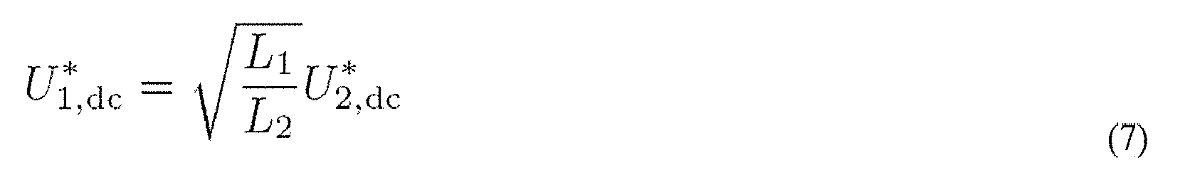
- In summary, the battery power P batt is a function of a product of the transmitter-side dc-bus voltage U 1,dc and the receiver-side dc-bus voltage U 2,dc, hence, the battery power can be controlled by adapting either of the dc-bus voltages. Therefore, three different control methods are possible:
- As a first option, as shown in
Fig. 4(a) , a controller can be used to adapt the reference value U 1,dc* for the transmitter-side dc-bus voltage U 1,dc based on a measured difference between the reference value I batt* and the battery current I batt. The reference value U2,dc* can be calculated based on a mathematical model which describes the power transfer, as shown above. A cascaded controller according to methods known from prior art can then be used to regulate the receiver-side dc-bus voltage U 2,dc to the reference value U 2,dc* with the receiver-side charging converter 15. The reference value U 2,dc* can also be added as a feed-forward to the reference value U 1,dc* of the transmitter-side dc-bus voltage U 1,dc. - As a second option, as shown in
Fig. 4(b) , a controller can be used to adapt the reference value U 2,dc* for the receiver-side dc-bus voltage U 2,dc based on the measured difference between the reference value I batt* and the battery current I batt. The reference value U 1,dc* can be calculated based on the mathematical model of equations (4), (5) and (6) which describes the power transfer. A cascaded controller according to methods known from prior art can then be used to regulate the transmitter-side dc-bus voltage U 1,dc to the reference value U 1,dc* with themains rectifier stage 11. The reference value U 1,dc*, or an equivalent value transformed to the receiver side, can also be used to derive a feed-forward signal which can be added to the output of the controller for the receiver-side dc-bus voltage U 2,dc. This feedforward value is the theoretical optimal value U 2,dc* for the receiver-side dc-bus voltage U 2,dc and is related to the reference value U 1,dc * by equation (6). Consequently, the controller adapting the reference value U 2,dc* must only correct for deviations from the theoretical optimal value due to e.g. a model mismatch - As a third option, as shown in
Fig. 4(c) , a controller can be used to adapt the reference value U 1,dc* for the transmitter-side dc-bus voltage U 1,dc based a measured difference between the reference value I batt* and the battery current I batt while the reference value U 2,dc* is calculated by another controller based on a measured difference between an input power P in input into the transmitter-side inverter stage 9 or thetransmitter coil 3 and a received power P out that is output by and e.g. also measured at the receiver coil 4 or at the receiver-side rectifier stage 13. In real-time, a power difference between the input power P in and the received power P out can by observed while the reference value U 1,dc* and the reference value U 2,dc* are adjusted by the controllers until the power difference is minimized and the battery current I batt is regulated to the reference value I batt*. - As shown in
Fig. 5 , an optimal value exists for the receiver-side dc-bus voltage U 2,dc where the relative difference between the input power P in and the received power P out is minimized. If changes in theresonant circuit 7 due to a misalignment of the receiver coil 4 with respect to thetransmitter coil 3, due to component tolerances, or due to parameter drifts occur, the optimal value changes and the receiver-side dc-bus voltage U 2,dc is, therefore, adjusted by the controllers. - In the control methods in which the transmitter-side dc-bus voltage U 1,dc is adapted with the PI-controller instead of the receiver-side dc-bus voltage U 2,dc the reaction time of the battery current control loop generally will be lower, due to the delay that is introduced by the communication across the air gap. Therefore, according to one embodiment, this control loop and critical parts (overheating, overcurrent and overvoltage protection) of the battery charging control are implemented on the receiver, which has a more direct access to the measurements.
- To calculate the reference values (6) and (7) accurately, an estimate of the magnetic coupling k is needed. If a feedback controller is used, also a pre-calculated, approximative value can be used and the controller will compensate for the estimation error. Additionaly or alternatively, the magnetic coupling can be estimated in real time, e.g., from measurements of the currents in the coils and an equivalent circuit.
- Alternatively, the reference value U 1,dc* and the reference value U 2,dc* can be determined from a voltage look-up table where the reference values obtained from an off-line calculation are stored in function of the transmitter and receiver coil currents and the switching frequency f sw of the transmitter-side inverter stage.
- The minimum communication for the optimal control is the transmission of the reference value U 1,dc* for the transmitter-side dc-bus voltage U 1,dc, which makes the system highly robust to a failure of the
communication channel 17. If communication is lost, U 1,dc remains constant, then this will be compensated for by the voltage controller on the receiver side. - A comparison of an efficiency of the power transfer that is achieved by the present invention compared to the efficiency of an inductive charging system with a fixed dc-bus voltage and a frequency control method known from prior art is shown in
Fig. 6 , which clearly shows the advantage of the present invention. - With the described methods, the transmitter-side dc-bus voltage U 1,dc, the receiver-side dc-bus voltage U 2,dc, and/or the switching frequency f sw are regulated to compensate for changes in the
resonant circuit 7 due to a misalignment of the receiver coil 4 with respect to thetransmitter coil 3, due to component tolerances, or due to parameter drifts. As shown inFig. 8 and Fig. 9, the changes can include a voltage gain G v = |U 2,dc/U1,dc|, which is higher than expected and a current gain G i = |Î 2/Î 1|, which is lower than expected. As a compensation, depending on the chosen control method, the transmitter-side dc-bus voltage U 1,dc and/or the receiver-side dc-bus voltage U 2,dc is adjusted such that the battery current I batt is regulated to its reference value I batt* despite the coil misalignment. Additionally, the switching frequency f sw is increased or decreased as well, for instance if a limit of a control range of the transmitter-side dc-bus voltage U 1,dc or the receiver-side dc-bus voltage U 2,dc is reached. Moreover, the changes in theresonant circuit 7 can include that the resonant frequency f 0 deviates from an expected value. This change is detected with the transmitter coilcurrent measurement 21 as described above and the switching frequency f sw is adjusted such that it remains in the inductive region close to the resonant frequency f 0 and that the switched current i 1,off stays at or close to its optimal value that minimizes the switching loss of the transmitter-side inverter stage 9. - In another embodiment with the same electrical circuit and functionality as either of the previously described embodiments, an on-time t on as shown in
Fig. 3 , during which the transmitter-side dc-bus voltage U 1,dc is applied to theresonant circuit 7 by the transmitter-side inverter stage 9, is adapted in addition to the switching frequency f sw according to a duty-cycle control method. Due to the duty-cycle control method, the on-time t on can be less than one half of a switching period T sw = 1/f sw. The switching frequency f sw can be adapted such that the transmitter coil current i 1(t) during a turn-on of a power semiconductor in a bridge-leg of the transmitter-side inverter stage 9 is always such that a turn-on switching loss is small. The on-time t on can be such that the optimal value of the switched current i 1,off is achieved and a switching loss during a turn-off of a power semiconductor in a bridge-leg of the transmitter-side inverter stage 9 is small. Alternatively, the on-time t on can be such that a change in the resonant circuit is compensated. - Further structural variants of the system are now described which can use the same control methods as described above.
- Another embodiment of the invention is shown in
Fig. 2(b) , where themains rectifier stage 11 of the transmitter-side power converter is realized as a six-switch buck+boost-type rectifier with two active power semiconductors and two diodes on each bridge leg, while the remaining parts of the electrical circuit and the functionality is equal to the embodiment shown inFig. 2(a) . An advantage of this alternative embodiment is that standard power modules can be used for the active power semiconductors. - In another embodiment of the invention, the
mains rectifier stage 11 of the embodiment shown inFig. 2(a) is realized as a boost-type rectifier with a cascaded dc-to-dc converter with buck capability, which is termed a boost+buck-type rectifier stage in prior art. The remainder of the electrical circuit and the functionality is the same as that of the embodiment shown inFig. 2(a) . - In another embodiment of the invention, the
mains rectifier stage 11 of the embodiment shown inFig. 2(a) realized by a buck-type rectifier as known from prior art. The buck-type rectifier can comprise three bridge legs equal to either those of the buck+boost-type rectifier of the embodiment inFig. 2(a) or those of the buck+boost-type rectifier of the embodiment inFig. 2(b) . However, it does not comprise the boost inductor L b1, the boost switch Tb1, and the diodes Db1-3, which are only needed for the boost mode. The remainder of the electrical circuit is the same as that of the embodiment inFig. 2(a) . An advantage of this embodiment is that it has a reduced complexity, however, the control of the transmitter-side bus voltage U 1,dc is limited as only a voltage reduction is possible, which reduces the robustness of the system. - In another embodiment, the transmitter-
side inverter stage 9 and themains rectifier stage 11 ofFig. 2(a) orFig. 2(b) are integrated while the remainder of the electrical circuit and the functionality remains the same as that of the embodiment shown inFig. 2(a) . The transmitter-side power converter 8 would then work as an indirect ac-to-ac converter or a direct ac-to-ac converter without an energy storing element in the transmitter-side dc-bus, using space-vector or phase-oriented control techniques. This is often termed a matrix converter. - In another embodiment, the receiver-
side rectifier stage 13 and receiver-side charging converter 15 are integrated, optionally in addition to an integration of the transmitter-side power converter 8, while the remainder of the electrical circuit and the functionality remains the same as that of the embodiment shown inFig. 2(a) . Active power semiconductors can be used instead of diodes in the receiver-side rectifier stage 13, thus forming a structure similar to a bridge-less rectifier with power factor correction as known from prior art. A measurement of the receiver coil current i 2(t) can be included in the receiver-side power converter 12 to synchronize the control of the active power semiconductors to the receiver coil current i 2(t).
Claims (13)
- An inductive power transfer system, in particular a battery charging system, for supplying electrical power from a transmitter-side subsystem connectable to a mains (1) to a receiver-side subsystem connectable to a load (2), the system comprising• a transmitter coil (3) and a receiver coil (4);• a transmitter-side power converter (8) comprising a mains rectifier stage (11) to power a transmitter-side dc-bus (10) and arranged to control a transmitter-side dc-bus voltage U 1,dc according to a corresponding reference value U 1,dc*;• a transmitter-side inverter stage (9) with a controllable turn-off time of switches of the transmitter-side inverter stage (9) to supply the transmitter (3) coil with an alternating current;• a receiver-side power converter (12) comprising a receiver-side rectifier stage (13) to rectify a voltage induced in the receiver coil (4) and to power a receiver-side dc-bus (14) and a receiver-side charging converter (15) arranged to control a receiver-side dc-bus voltage U 2,dc according to a corresponding reference value U 2,dc*;• one or more power controllers (19, 18) arranged to determine a value that is indicative of a power transfer efficiency of the power transfer and to calculate, from this value indicative of the power transfer efficiency, the reference values U 1,dc*, U2,dc* for the transmitter-side dc-bus voltage U 1,dc and the receiver-side dc-bus voltage U 2,dc;• an inverter stage switching controller (20) arranged to control the turn-off time of the switches of the transmitter-side inverter stage (9) to at least approximately minimise switching losses in the transmitter-side inverter stage (9).
- The inductive power transfer system of claim 1, comprising a communication channel (17) for transmitting the reference value U 1,dc* for the transmitter-side dc-bus voltage U 1,dc from the receiver-side subsystem to the transmitter-side subsystem.
- The inductive power transfer system of one of claims 1 or 2, wherein the value that is indicative of the power transfer efficiency is a magnetic coupling (k) between the transmitter coil (3) and receiver coil (4).
- The inductive power transfer system of one of claims 1 or 2, wherein the value that is indicative of the power transfer efficiency is computed from a measurement of an input power P in input into the transmitter-side inverter stage (9) or the transmitter coil (3) and a measurement of a received power P out that is output by the receiver coil (4) or the receiver-side rectifier stage (13).
- The inductive power transfer system of one of claims 1 or 2, wherein at least one of the reference values U 1,dc*, U 2,dc* for the transmitter-side dc-bus voltage U 1,dc and the receiver-side dc-bus voltage U 2,dc is determined from a look-up table wherein reference values obtained from an off-line calculation are stored in function of transmitter and receiver coil currents and a switching frequency f sw of the transmitter-side inverter stage (9).
- The inductive power transfer system of one of the preceding claims, wherein the one or more power controllers (19, 18) are configured• to compute the reference value U 2,dc* for the receiver-side dc-bus voltage U 2,dc from a measured difference between a load current I batt.and a reference value I batt* for the load current; and• to compute the reference value U 1,dc* for the transmitter-side dc-bus voltage U 1,dc from the reference value I batt* for the load current and a measured value of the load voltage U batt.
- The inductive power transfer system of one of the preceding claims, wherein the inverter stage switching controller (20) is arranged to control the transmitter-side inverter stage (9) in an inductive region close to the resonant frequency f 0 of the transmitter for a switch-off current i 1,off, corresponding to a value of the transmitter coil current i i(t) at the time of commutation, that is at a value that minimizes a switching loss of the transmitter-side inverter stage (9).
- The inductive power transfer system of one of the claims 1 to 7, wherein the inverter stage switching controller (20) is arranged to control the turn-off time of the switches of the transmitter-side inverter stage (9) for a switch-off current i 1,off to follow a switch-off current reference value.
- The inductive power transfer system of one of the claims 1 to 7, wherein the inverter stage switching controller (20) is arranged to estimate a power loss in the semiconductor switches of the transmitter-side inverter stage (9) and to perform an iterative search procedure, varying the turn-off time of the switches of the transmitter-side inverter stage (9) to minimise the power loss.
- The inductive power transfer system of one of the claims 1 to 7, wherein the inverter stage switching controller (20) is arranged to control the turn-off time of the switches of the transmitter-side inverter stage (9) for the transmitter coil current i 1(t) to have a constant phase shift relative to the output voltage u 1(t) of the transmitter-side inverter stage (9)
- A transmitter side subsystem of an inductive power transfer system, connectable to a mains (1) and being able to supply electrical power to a receiver-side subsystem, the transmitter side subsystem comprising• a transmitter coil (3);• a transmitter-side power converter (8) comprising a mains rectifier stage (11) to power a transmitter-side dc-bus (10) and arranged to control a transmitter-side dc-bus voltage U 1,dc according to a corresponding reference value U 1,dc*, and• a transmitter-side inverter stage (9) with a controllable turn-off time of switches of the transmitter-side inverter stage (9) to supply the transmitter (3) coil with an alternating current;• transmitter-side communication means for receiving the reference value U 1,dc* for the transmitter-side dc-bus voltage U 1,dc from the receiver-side subsystem;• an inverter stage switching controller (20) arranged to control the turn-off time of the switches of the transmitter-side inverter stage (9) to at least approximately minimise switching losses in the transmitter-side inverter stage transmitter-side inverter stage (9).
- A receiver side subsystem of an inductive power transfer system, the receiver-side subsystem being connectable to a load (2) and being able to receive electrical power from a transmitter-side subsystem, the receiver-side subsystem comprising• a receiver coil (4);• a receiver-side power converter (12) comprising a receiver-side rectifier stage (13) to rectify a voltage induced in the receiver coil (4) and to power a receiver-side dc-bus (14) and a receiver-side charging converter (15) arranged to control a receiver-side dc-bus voltage U 2,dc according to a corresponding reference value U 2,dc*;• a receiver-side controller (19) arranged to determine a value that is indicative of a power transfer efficiency of the power transfer and to calculate, from this value indicative of the power transfer efficiency, reference values U 1,dc*, U 2,dc* for a transmitter-side dc-bus voltage U 1,dc and the receiver-side dc-bus voltage U 2,dc;• receiver-side communication means for transmitting the reference value U 1,dc* for the transmitter-side dc-bus voltage U 1,dc from the receiver-side subsystem to the transmitter-side subsystem.
- A method for controlling an inductive power transfer system, in particular a battery charging system, for supplying electrical power from a transmitter-side subsystem connectable to a mains (1) to a receiver-side subsystem connectable to a load (2), the inductive power transfer system comprising• a transmitter coil (3) and a receiver coil (4);• a transmitter-side power converter (8) comprising a mains rectifier stage (11) to power a transmitter-side dc-bus (10);• a transmitter-side inverter stage (9) with a controllable turn-off time of switches of the transmitter-side inverter stage (9) to supply the transmitter (3) coil with an alternating current;• a receiver-side power converter (12) comprising a receiver-side rectifier stage (13) to rectify a voltage induced in the receiver coil (4) and to power a receiver-side dc-bus (14) and a receiver-side charging converter (15) arranged to control a receiver-side dc-bus voltage U 2,dc according to a corresponding reference value U 2,dc*;the method comprising the steps of:• determining a value that is indicative of a power transfer efficiency of the power transfer and calculating, from this value indicative of the power transfer efficiency, reference values U 1,dc*, U 2,dc* for a transmitter-side dc-bus voltage U 1,dc and a receiver-side dc-bus voltage U 2,dc;• controlling the mains rectifier stage (11) for the transmitter-side dc-bus voltage U 1,dc of the transmitter-side dc-bus (10) to follow the corresponding reference value U 1,dc*;• controlling the receiver-side charging converter (15) for the receiver-side dc-bus voltage U 2,dc of the receiver-side dc-bus (14) to follow the corresponding reference value U 2,dc*;• controlling the turn-off time of the switches of the transmitter-side inverter stage (9) to at least approximately minimise switching losses in the transmitter-side inverter stage transmitter-side inverter stage (9).
Priority Applications (3)
| Application Number | Priority Date | Filing Date | Title |
|---|---|---|---|
| EP14162789.3A EP2928038A1 (en) | 2014-03-31 | 2014-03-31 | Inductive power transfer system and method for operating an inductive power transfer system |
| US14/672,803 US9843199B2 (en) | 2014-03-31 | 2015-03-30 | Inductive power transfer system and method for operating an inductive power transfer system |
| CN201510146684.0A CN104953683B (en) | 2014-03-31 | 2015-03-31 | Induced power transmission system and the method for answering the system of power transmission for operation sense |
Applications Claiming Priority (1)
| Application Number | Priority Date | Filing Date | Title |
|---|---|---|---|
| EP14162789.3A EP2928038A1 (en) | 2014-03-31 | 2014-03-31 | Inductive power transfer system and method for operating an inductive power transfer system |
Publications (1)
| Publication Number | Publication Date |
|---|---|
| EP2928038A1 true EP2928038A1 (en) | 2015-10-07 |
Family
ID=50389984
Family Applications (1)
| Application Number | Title | Priority Date | Filing Date |
|---|---|---|---|
| EP14162789.3A Withdrawn EP2928038A1 (en) | 2014-03-31 | 2014-03-31 | Inductive power transfer system and method for operating an inductive power transfer system |
Country Status (3)
| Country | Link |
|---|---|
| US (1) | US9843199B2 (en) |
| EP (1) | EP2928038A1 (en) |
| CN (1) | CN104953683B (en) |
Cited By (10)
| Publication number | Priority date | Publication date | Assignee | Title |
|---|---|---|---|---|
| CN106253397A (en) * | 2016-08-23 | 2016-12-21 | 北京新能源汽车股份有限公司 | A kind of integrated charger and energy emission system |
| CN106253285A (en) * | 2016-10-12 | 2016-12-21 | 北京新能源汽车股份有限公司 | A kind of vehicle-mounted bidirectional charger, electric automobile and mains by harmonics compensation method |
| CN106655431A (en) * | 2016-12-21 | 2017-05-10 | 江西佰仕通电子科技有限公司 | Charger circuit capable of automatically adjusting current |
| WO2017211557A1 (en) * | 2016-06-07 | 2017-12-14 | Robert Bosch Gmbh | Transmission system for contactlessly transmitting energy |
| JP2019110753A (en) * | 2016-02-05 | 2019-07-04 | グァンドン オッポ モバイル テレコミュニケーションズ コーポレーション リミテッドGuangdong Oppo Mobile Telecommunications Corp., Ltd. | Adapter and charge control method |
| WO2020008198A1 (en) * | 2018-07-04 | 2020-01-09 | Imperial College Innovations Ltd | Transmitter and receiver circuitry for power converter systems |
| EP3748812A1 (en) * | 2016-02-03 | 2020-12-09 | General Electric Company | Method and system for protecting a wireless power transfer system |
| EP3724977A4 (en) * | 2017-12-12 | 2021-12-01 | Phasetown, LLC | Power factor adjustment method and apparatus through the phase control |
| WO2022023779A1 (en) * | 2020-07-31 | 2022-02-03 | Energy Research Lab Ltd | An inverter |
| US11955805B2 (en) | 2016-02-03 | 2024-04-09 | General Electric Company | System and method for protecting a wireless power transfer system |
Families Citing this family (81)
| Publication number | Priority date | Publication date | Assignee | Title |
|---|---|---|---|---|
| US9673784B2 (en) | 2013-11-21 | 2017-06-06 | Apple Inc. | Using pulsed biases to represent DC bias for charging |
| US10116230B2 (en) | 2013-12-30 | 2018-10-30 | Eaton Capital Unlimited Company | Methods, circuits and articles of manufacture for configuring DC output filter circuits |
| EP3111531A1 (en) | 2014-02-23 | 2017-01-04 | Apple Inc. | Adjusting filter in a coupled coil system |
| KR20180069107A (en) | 2014-02-23 | 2018-06-22 | 애플 인크. | Impedance matching for inductive power transfer systems |
| JP6588190B2 (en) * | 2014-03-28 | 2019-10-09 | 株式会社デンソー | Wireless power feeder |
| US9525376B2 (en) | 2014-05-13 | 2016-12-20 | Gbox, Llc | Wound field synchronous machine with resonant field exciter |
| US10032557B1 (en) | 2014-05-29 | 2018-07-24 | Apple Inc. | Tuning of primary and secondary resonant frequency for improved efficiency of inductive power transfer |
| US9537353B1 (en) | 2014-06-03 | 2017-01-03 | Apple Inc. | Methods for detecting mated coils |
| US9685814B1 (en) | 2014-06-13 | 2017-06-20 | Apple Inc. | Detection of coil coupling in an inductive charging system |
| US9590525B2 (en) * | 2014-07-03 | 2017-03-07 | Eaton Capital | Wireless power transfer systems using load feedback |
| US9813041B1 (en) | 2014-07-31 | 2017-11-07 | Apple Inc. | Automatic boost control for resonant coupled coils |
| US10014733B2 (en) | 2014-08-28 | 2018-07-03 | Apple Inc. | Temperature management in a wireless energy transfer system |
| US10193372B2 (en) | 2014-09-02 | 2019-01-29 | Apple Inc. | Operating an inductive energy transfer system |
| US9647455B2 (en) * | 2014-09-30 | 2017-05-09 | The Boeing Company | EMI filter systems and methods for parallel modular converters |
| US9984815B2 (en) | 2014-12-22 | 2018-05-29 | Eaton Capital Unlimited Company | Wireless power transfer apparatus and power supplies including overlapping magnetic cores |
| US10038324B2 (en) * | 2015-01-06 | 2018-07-31 | Eaton Intelligent Power Limited | Methods, circuits and articles of manufacture for controlling wireless power transfer responsive to controller circuit states |
| US9640976B2 (en) * | 2015-02-26 | 2017-05-02 | Ut-Battelle, Llc | Overvoltage protection system for wireless power transfer systems |
| DE112016001489T5 (en) * | 2015-03-31 | 2018-01-04 | Tdk Corporation | WIRELESS ENERGY RECEIVING DEVICE AND WIRELESS POWER TRANSMISSION DEVICE |
| US10116144B2 (en) | 2015-05-22 | 2018-10-30 | Eaton Intelligent Power Limited | Wireless power transfer apparatus using enclosures with enhanced magnetic features and methods of fabricating the same |
| US10666084B2 (en) | 2015-07-10 | 2020-05-26 | Apple Inc. | Detection and notification of an unpowered releasable charging device |
| US9819215B2 (en) * | 2015-07-17 | 2017-11-14 | Hon Hai Precision Industry Co., Ltd. | Wireless charging system |
| US10020759B2 (en) | 2015-08-04 | 2018-07-10 | The Boeing Company | Parallel modular converter architecture for efficient ground electric vehicles |
| US10186908B2 (en) * | 2015-08-04 | 2019-01-22 | Ningbo Weie Electronic Technology Co., Ltd. | Efficient power transmitting terminal, contactless power transmission device and power transmission method |
| CN106477436B (en) * | 2015-08-25 | 2019-11-12 | 奥的斯电梯公司 | Electromechanical propulsion system with Wireless power transmission system |
| US10122217B2 (en) * | 2015-09-28 | 2018-11-06 | Apple Inc. | In-band signaling within wireless power transfer systems |
| CN106560975B (en) * | 2015-10-02 | 2021-06-01 | 松下知识产权经营株式会社 | Power receiving device and wireless power transmission system |
| US10582726B2 (en) | 2015-10-21 | 2020-03-10 | Rai Strategic Holdings, Inc. | Induction charging for an aerosol delivery device |
| US20170117813A1 (en) * | 2015-10-21 | 2017-04-27 | Quanta Computer Inc. | Method and system for testing a power supply unit |
| US10611251B2 (en) * | 2015-11-13 | 2020-04-07 | Nio Usa, Inc. | Distributed processing network for rechargeable electric vehicle tracking and routing |
| US10131238B2 (en) | 2015-11-13 | 2018-11-20 | Nio Usa, Inc. | Charging transmission line under roadway for moving electric vehicle |
| US10160339B2 (en) | 2015-11-13 | 2018-12-25 | Nio Usa, Inc. | Smart grid management |
| JP6299779B2 (en) * | 2016-02-02 | 2018-03-28 | トヨタ自動車株式会社 | Power transmission device and power transmission system |
| GB2547452B (en) * | 2016-02-18 | 2019-06-12 | Inductronics Tech Limited | An inductive coupling device and system |
| CN107634673A (en) * | 2016-07-18 | 2018-01-26 | 维谛技术有限公司 | The Zero voltage transition circuit of Sofe Switch auxiliary circuit, three-level three-phase |
| US10263526B2 (en) * | 2016-08-02 | 2019-04-16 | Smart Prong Technologies, Inc. | Electrical circuit for isolated voltage conversion |
| EP3280030B1 (en) * | 2016-08-04 | 2023-08-30 | General Electric Company | System and method for charging receiver devices |
| US10763698B2 (en) * | 2016-08-23 | 2020-09-01 | The Penn State Research Foundation | Self-regulated reconfigurable resonant voltage/current-mode method and device for extended-range inductive power transmission |
| WO2018048312A1 (en) | 2016-09-06 | 2018-03-15 | Powerbyproxi Limited | An inductive power transmitter |
| US10644531B1 (en) | 2016-09-22 | 2020-05-05 | Apple Inc. | Adaptable power rectifier for wireless charger system |
| US10601250B1 (en) | 2016-09-22 | 2020-03-24 | Apple Inc. | Asymmetric duty control of a half bridge power converter |
| EP3523156B1 (en) * | 2016-10-10 | 2023-06-07 | iN2POWER NV | Energy transmitter and receiver module |
| EP3322076B1 (en) * | 2016-11-14 | 2020-02-05 | Siemens Aktiengesellschaft | Switching power supply with resonant converter |
| CA3045081A1 (en) * | 2016-12-02 | 2018-06-07 | Rai Strategic Holdings, Inc. | Induction charging for an aerosol delivery device |
| US10919401B2 (en) * | 2017-01-12 | 2021-02-16 | Ford Global Technologies, Llc | Integrated wireless power transfer system |
| US9919610B1 (en) * | 2017-01-12 | 2018-03-20 | The Florida International University Board Of Trustees | Wireless power electronics and controls |
| US10742071B2 (en) | 2017-01-19 | 2020-08-11 | Qualcomm Incorporated | Wireless power transfer for stationary applications |
| US10369891B2 (en) * | 2017-02-20 | 2019-08-06 | Ford Global Technologies, Llc | Wireless power transfer system parameter estimation |
| JP6680243B2 (en) * | 2017-03-02 | 2020-04-15 | オムロン株式会社 | Non-contact power supply device |
| CN108574345A (en) * | 2017-03-10 | 2018-09-25 | 重庆邮电大学 | A kind of wireless power transmission equipment transmitting terminal self-adapting tuning device and tuning methods |
| US10523063B2 (en) | 2017-04-07 | 2019-12-31 | Apple Inc. | Common mode noise compensation in wireless power systems |
| US10389274B2 (en) | 2017-04-07 | 2019-08-20 | Apple Inc. | Boosted output inverter for electronic devices |
| US20180337559A1 (en) * | 2017-05-18 | 2018-11-22 | Integrated Device Technology, Inc. | Power limiting in a wireless power transmitter |
| CN106972649A (en) * | 2017-05-19 | 2017-07-21 | 深圳维思加通信技术有限公司 | Wireless charging system |
| CN107872101B (en) * | 2017-11-24 | 2019-11-15 | 深圳市文鼎创数据科技有限公司 | A kind of NFC antenna electricity getting device |
| US10903691B2 (en) * | 2017-11-29 | 2021-01-26 | Tdk Corporation | Wireless power receiver and wireless power transmission system using the same |
| JP7003708B2 (en) * | 2018-02-07 | 2022-01-21 | オムロン株式会社 | Contactless power supply |
| WO2019192733A1 (en) * | 2018-04-06 | 2019-10-10 | Abb Schweiz Ag | A power transfer system for electric vehicles and a control method thereof |
| EP3776791A1 (en) * | 2018-04-06 | 2021-02-17 | ABB Schweiz AG | A power transfer system for electric vehicles and a control method thereof |
| US11975620B2 (en) | 2018-04-23 | 2024-05-07 | ABB E-mobility B.V. | Power transfer system for electric vehicles and a control method thereof |
| SG11202011091QA (en) * | 2018-05-10 | 2020-12-30 | Toshiba Kk | Dc transformation system |
| US10594226B2 (en) * | 2018-08-13 | 2020-03-17 | Dean Technology Inc. | Adjustable zero voltage to high voltage power supply |
| US11005298B2 (en) * | 2018-08-29 | 2021-05-11 | Integrated Device Technology, Inc. | Wireless power maximum efficiency tracking by system control |
| JP7205169B2 (en) * | 2018-11-01 | 2023-01-17 | オムロン株式会社 | Contactless power supply |
| US11631998B2 (en) * | 2019-01-10 | 2023-04-18 | Hengchun Mao | High performance wireless power transfer and power conversion technologies |
| ES2934079T3 (en) * | 2019-02-05 | 2023-02-16 | Mahle Int Gmbh | Wireless power transfer systems for electric vehicles |
| CN110048514B (en) * | 2019-02-22 | 2020-12-29 | 苏州加士革电子科技有限公司 | Wireless power transmission system based on primary side feedback controller |
| US11463019B2 (en) * | 2019-03-25 | 2022-10-04 | Semiconductor Components Industries, Llc | Power supply system for optimizing a performance metric using artificial intelligence |
| JP2021002984A (en) * | 2019-06-25 | 2021-01-07 | Tdk株式会社 | Wireless power transmission device and wireless power transmission system |
| US11557956B2 (en) * | 2019-07-12 | 2023-01-17 | Nissan Motor Co., Ltd. | Power conversion device and method for converting power from a power supply |
| CN111433075B (en) * | 2019-09-05 | 2023-05-09 | 香港应用科技研究院有限公司 | Intelligent power supply center |
| US11621645B2 (en) * | 2020-06-04 | 2023-04-04 | Stmicroelectronics International N.V. | Methods and device to drive a transistor for synchronous rectification |
| CN111740505B (en) * | 2020-07-03 | 2022-02-08 | 浙江大学 | Method for realizing PFC (Power factor correction) only through primary side phase shift control |
| JP7384136B2 (en) | 2020-09-18 | 2023-11-21 | 株式会社明電舎 | Bidirectional isolated DC/DC converter and its control method |
| CN112260543B (en) * | 2020-09-19 | 2022-06-24 | 许继电源有限公司 | High-gain high-frequency isolation bidirectional cascade DC/DC converter and control method thereof |
| CN112448446B (en) * | 2020-11-11 | 2023-06-20 | 许继集团有限公司 | Static wireless charging method and system for electric automobile |
| US11784512B2 (en) * | 2021-08-06 | 2023-10-10 | Apple Inc. | Enhanced communications for wireless power transfer |
| US20230064783A1 (en) * | 2021-09-02 | 2023-03-02 | Rivian Ip Holdings, Llc | Dual active bridge converter control with switching loss distribution |
| CN114552797A (en) * | 2021-12-28 | 2022-05-27 | 温州尚明节能科技有限公司 | Underwater low-voltage wireless power supply device |
| CN114785168B (en) * | 2022-05-10 | 2023-05-19 | 西南交通大学 | Maximum power tracking method of inductive energy collection system based on impedance matching |
| CN116191828A (en) * | 2022-06-06 | 2023-05-30 | 浙江网新智能技术有限公司 | Cascade power supply system with self-adaptive adjustment of intermediate bus voltage |
| FR3140490A1 (en) * | 2022-09-30 | 2024-04-05 | Valeo Systemes De Controle Moteur | Secondary resonant circuit |
Citations (4)
| Publication number | Priority date | Publication date | Assignee | Title |
|---|---|---|---|---|
| CH698918B1 (en) | 2006-02-20 | 2009-12-15 | Eth Zuerich Eth Transfer | Device for converting three phase alternating current voltage into direct current voltage for three phase buck-boost converter pulse rectifier system, has bridge section whose phase input has negative value of input potential of section |
| WO2012005607A2 (en) * | 2010-06-30 | 2012-01-12 | Auckland Uniservices Limited | Inductive power transfer system |
| US20130088088A1 (en) * | 2011-09-05 | 2013-04-11 | Peter Wambsganss | Circuitry And Method For Inductive Power Transmission |
| US20140015330A1 (en) * | 2012-07-10 | 2014-01-16 | Samsung Electronics Co., Ltd. | Method and power transmitter for controlling power transmission |
Family Cites Families (15)
| Publication number | Priority date | Publication date | Assignee | Title |
|---|---|---|---|---|
| US7675759B2 (en) * | 2006-12-01 | 2010-03-09 | Flextronics International Usa, Inc. | Power system with power converters having an adaptive controller |
| JP4400632B2 (en) * | 2007-02-20 | 2010-01-20 | Tdk株式会社 | Switching power supply |
| IL184358A (en) * | 2007-07-02 | 2011-04-28 | Univ Ben Gurion | Method and circuitry for improving the magnitude and shape of the output current of switching power converters |
| US8654483B2 (en) * | 2009-11-09 | 2014-02-18 | Cirrus Logic, Inc. | Power system having voltage-based monitoring for over current protection |
| WO2011151940A1 (en) * | 2010-05-31 | 2011-12-08 | 三菱電機株式会社 | Power conversion device |
| US9007002B2 (en) * | 2010-06-15 | 2015-04-14 | Ihi Corporation | Device and method for power-saving driving of device having same load pattern |
| JP5306306B2 (en) * | 2010-10-19 | 2013-10-02 | オムロンオートモーティブエレクトロニクス株式会社 | Switching power supply |
| US9263968B2 (en) * | 2011-06-22 | 2016-02-16 | Eetrex, Inc. | Bidirectional inverter-charger |
| CN102315698B (en) * | 2011-08-30 | 2013-06-12 | 矽力杰半导体技术(杭州)有限公司 | Magnetic field coupling-type non-contact electric energy transmission device |
| WO2013136755A1 (en) * | 2012-03-16 | 2013-09-19 | パナソニック株式会社 | Power feed device of inductive charging device |
| CN102969776B (en) * | 2012-12-03 | 2014-12-10 | 中国科学院电工研究所 | Wireless charging device of electronic automobile |
| WO2014160048A1 (en) * | 2013-03-14 | 2014-10-02 | Enphase Energy, Inc. | Method and apparatus for determining a bridge mode for power conversion |
| JP5618022B1 (en) * | 2013-06-11 | 2014-11-05 | 住友電気工業株式会社 | Inverter device |
| JP6286793B2 (en) * | 2014-01-24 | 2018-03-07 | 株式会社日立情報通信エンジニアリング | DC-DC converter, secondary battery charge / discharge system, and control method of DC-DC converter |
| JP6153491B2 (en) * | 2014-03-28 | 2017-06-28 | オムロンオートモーティブエレクトロニクス株式会社 | Power supply |
-
2014
- 2014-03-31 EP EP14162789.3A patent/EP2928038A1/en not_active Withdrawn
-
2015
- 2015-03-30 US US14/672,803 patent/US9843199B2/en not_active Expired - Fee Related
- 2015-03-31 CN CN201510146684.0A patent/CN104953683B/en not_active Expired - Fee Related
Patent Citations (4)
| Publication number | Priority date | Publication date | Assignee | Title |
|---|---|---|---|---|
| CH698918B1 (en) | 2006-02-20 | 2009-12-15 | Eth Zuerich Eth Transfer | Device for converting three phase alternating current voltage into direct current voltage for three phase buck-boost converter pulse rectifier system, has bridge section whose phase input has negative value of input potential of section |
| WO2012005607A2 (en) * | 2010-06-30 | 2012-01-12 | Auckland Uniservices Limited | Inductive power transfer system |
| US20130088088A1 (en) * | 2011-09-05 | 2013-04-11 | Peter Wambsganss | Circuitry And Method For Inductive Power Transmission |
| US20140015330A1 (en) * | 2012-07-10 | 2014-01-16 | Samsung Electronics Co., Ltd. | Method and power transmitter for controlling power transmission |
Non-Patent Citations (4)
| Title |
|---|
| B. GOELDI; S. REICHERT; J. TRITSCHLER: "Design and Dimensioning of a Highly Efficient 22 kW Bidirectional Inductive Charger for E-Mobility", PROC. INT. EXHIBITION AND CONF FOR POWER ELECTRONICS (PCIM EUROPE, 2013, pages 1496 - 1503 |
| G. ORTIZ; H. UEMURA; D. BORTIS; J. W. KOLAR; APELDOORN: "Modeling of Soft-Switching Losses of IGBTs in High-Power High-Efficiency Dual-Active-Bridge DC/DC Converters", IEEE TRANS. ELECTRON DEVICES, vol. 60, no. 2, February 2013 (2013-02-01), pages 587 - 597, XP011487986, DOI: doi:10.1109/TED.2012.2223215 |
| GABRIEL ORTIZ ET AL: "Modeling of Soft-Switching Losses of IGBTs in High-Power High-Efficiency Dual-Active-Bridge DC/DC Converters", IEEE TRANSACTIONS ON ELECTRON DEVICES, IEEE SERVICE CENTER, PISACATAWAY, NJ, US, vol. 60, no. 2, 1 February 2013 (2013-02-01), pages 587 - 597, XP011487986, ISSN: 0018-9383, DOI: 10.1109/TED.2012.2223215 * |
| T. NUSSBAUMER; M. BAUMANN; J. W. KOLAR: "Comprehensive Design of a Three-Phase Three-Switch Buck-Type PWM Rectifier", IEEE TRANS. POWER ELECTRONICS, vol. 22, no. 2, March 2007 (2007-03-01), pages 551 - 562, XP011172378, DOI: doi:10.1109/TPEL.2006.889987 |
Cited By (16)
| Publication number | Priority date | Publication date | Assignee | Title |
|---|---|---|---|---|
| EP3748812A1 (en) * | 2016-02-03 | 2020-12-09 | General Electric Company | Method and system for protecting a wireless power transfer system |
| US11955805B2 (en) | 2016-02-03 | 2024-04-09 | General Electric Company | System and method for protecting a wireless power transfer system |
| US11949240B2 (en) | 2016-02-03 | 2024-04-02 | General Electric Company | Method and system for protecting a wireless power transfer system |
| US11394239B2 (en) | 2016-02-03 | 2022-07-19 | General Electric Company | Method and system for protecting a wireless power transfer system |
| JP2019110753A (en) * | 2016-02-05 | 2019-07-04 | グァンドン オッポ モバイル テレコミュニケーションズ コーポレーション リミテッドGuangdong Oppo Mobile Telecommunications Corp., Ltd. | Adapter and charge control method |
| US10804752B2 (en) | 2016-06-07 | 2020-10-13 | Robert Bosch Gmbh | Transmission system for contactlessly transmitting energy |
| WO2017211557A1 (en) * | 2016-06-07 | 2017-12-14 | Robert Bosch Gmbh | Transmission system for contactlessly transmitting energy |
| CN106253397A (en) * | 2016-08-23 | 2016-12-21 | 北京新能源汽车股份有限公司 | A kind of integrated charger and energy emission system |
| CN106253285A (en) * | 2016-10-12 | 2016-12-21 | 北京新能源汽车股份有限公司 | A kind of vehicle-mounted bidirectional charger, electric automobile and mains by harmonics compensation method |
| CN106655431B (en) * | 2016-12-21 | 2023-05-12 | 江西佰仕通电子科技有限公司 | Automatic current regulation charger circuit |
| CN106655431A (en) * | 2016-12-21 | 2017-05-10 | 江西佰仕通电子科技有限公司 | Charger circuit capable of automatically adjusting current |
| EP3724977A4 (en) * | 2017-12-12 | 2021-12-01 | Phasetown, LLC | Power factor adjustment method and apparatus through the phase control |
| WO2020008198A1 (en) * | 2018-07-04 | 2020-01-09 | Imperial College Innovations Ltd | Transmitter and receiver circuitry for power converter systems |
| WO2022023779A1 (en) * | 2020-07-31 | 2022-02-03 | Energy Research Lab Ltd | An inverter |
| WO2022023780A1 (en) * | 2020-07-31 | 2022-02-03 | Energy Research Lab Ltd | An inverter |
| WO2022023778A1 (en) * | 2020-07-31 | 2022-02-03 | Energy Research Lab Ltd | An inverter |
Also Published As
| Publication number | Publication date |
|---|---|
| US20150280455A1 (en) | 2015-10-01 |
| US9843199B2 (en) | 2017-12-12 |
| CN104953683B (en) | 2019-02-15 |
| CN104953683A (en) | 2015-09-30 |
Similar Documents
| Publication | Publication Date | Title |
|---|---|---|
| US9843199B2 (en) | Inductive power transfer system and method for operating an inductive power transfer system | |
| CN110139775B (en) | Method for controlling a charging device on board an electric or hybrid vehicle | |
| TWI706622B (en) | System architecture for battery charger based on gan-based power devices and dc-to-dc converter used therein | |
| Bosshard et al. | Control method for inductive power transfer with high partial-load efficiency and resonance tracking | |
| Jung et al. | High efficiency bidirectional LLC resonant converter for 380V DC power distribution system using digital control scheme | |
| EP2783444B1 (en) | Renewable energy power generation systems | |
| US20180062528A1 (en) | Interleaved resonant converter | |
| US8503208B2 (en) | Converter for single-phase and three-phase operation, D.C. voltage supply and battery charger | |
| US8411473B2 (en) | Three-phase power supply with three-phase three-level DC/DC converter | |
| US11056979B2 (en) | Power conversion apparatus | |
| KR20140117596A (en) | Wireless power transfer system | |
| US11065968B2 (en) | Integrated multi-source IPT system | |
| US11557921B2 (en) | Wireless power system | |
| Prasuna et al. | Improvement in power factor & thd using dual boost converter | |
| Zanatta et al. | Design and implementation of a two-stage resonant converter for wide output range operation | |
| Tritschler et al. | Comparison of different control strategies for series-series compensated inductive power transmission systems | |
| Sanchez et al. | An ultra-low weight bidirectional back-end PFC topology | |
| Frechter et al. | On the minimal loading of sensorless series-series compensated inductive WPT link operating at load independent voltage output frequency without feedback | |
| Pan et al. | A PS/S current-fed IPT system with variable capacitors for achieving ZPA operation | |
| Zanatta et al. | Analysis and performance evaluation of a two-stage resonant converter for wide voltage range operation | |
| US11791739B2 (en) | AC-AC converter | |
| KR20220044996A (en) | Vehicle-Grid-Home Power Interface | |
| Singh et al. | Bridgeless modified high-step-up gain SEPIC PFC converter based charger for light EVs battery | |
| Zanatta et al. | A Two-Stage Twin-Bus Buck Converter for Battery Charging Applications | |
| Li et al. | A high frequency AC-AC converter for inductive power transfer (IPT) applications |
Legal Events
| Date | Code | Title | Description |
|---|---|---|---|
| PUAI | Public reference made under article 153(3) epc to a published international application that has entered the european phase |
Free format text: ORIGINAL CODE: 0009012 |
|
| AK | Designated contracting states |
Kind code of ref document: A1 Designated state(s): AL AT BE BG CH CY CZ DE DK EE ES FI FR GB GR HR HU IE IS IT LI LT LU LV MC MK MT NL NO PL PT RO RS SE SI SK SM TR |
|
| AX | Request for extension of the european patent |
Extension state: BA ME |
|
| 17P | Request for examination filed |
Effective date: 20160329 |
|
| RBV | Designated contracting states (corrected) |
Designated state(s): AL AT BE BG CH CY CZ DE DK EE ES FI FR GB GR HR HU IE IS IT LI LT LU LV MC MK MT NL NO PL PT RO RS SE SI SK SM TR |
|
| RAP1 | Party data changed (applicant data changed or rights of an application transferred) |
Owner name: ABB SCHWEIZ AG |
|
| STAA | Information on the status of an ep patent application or granted ep patent |
Free format text: STATUS: THE APPLICATION HAS BEEN WITHDRAWN |
|
| 18W | Application withdrawn |
Effective date: 20190430 |