EP1852962A1 - Power conversion apparatus - Google Patents
Power conversion apparatus Download PDFInfo
- Publication number
- EP1852962A1 EP1852962A1 EP06714137A EP06714137A EP1852962A1 EP 1852962 A1 EP1852962 A1 EP 1852962A1 EP 06714137 A EP06714137 A EP 06714137A EP 06714137 A EP06714137 A EP 06714137A EP 1852962 A1 EP1852962 A1 EP 1852962A1
- Authority
- EP
- European Patent Office
- Prior art keywords
- power
- voltage
- conversion apparatus
- output voltage
- power conversion
- Prior art date
- Legal status (The legal status is an assumption and is not a legal conclusion. Google has not performed a legal analysis and makes no representation as to the accuracy of the status listed.)
- Withdrawn
Links
Images


Classifications
-
- H—ELECTRICITY
- H02—GENERATION; CONVERSION OR DISTRIBUTION OF ELECTRIC POWER
- H02M—APPARATUS FOR CONVERSION BETWEEN AC AND AC, BETWEEN AC AND DC, OR BETWEEN DC AND DC, AND FOR USE WITH MAINS OR SIMILAR POWER SUPPLY SYSTEMS; CONVERSION OF DC OR AC INPUT POWER INTO SURGE OUTPUT POWER; CONTROL OR REGULATION THEREOF
- H02M7/00—Conversion of ac power input into dc power output; Conversion of dc power input into ac power output
- H02M7/42—Conversion of dc power input into ac power output without possibility of reversal
- H02M7/44—Conversion of dc power input into ac power output without possibility of reversal by static converters
- H02M7/48—Conversion of dc power input into ac power output without possibility of reversal by static converters using discharge tubes with control electrode or semiconductor devices with control electrode
- H02M7/483—Converters with outputs that each can have more than two voltages levels
-
- H—ELECTRICITY
- H02—GENERATION; CONVERSION OR DISTRIBUTION OF ELECTRIC POWER
- H02J—CIRCUIT ARRANGEMENTS OR SYSTEMS FOR SUPPLYING OR DISTRIBUTING ELECTRIC POWER; SYSTEMS FOR STORING ELECTRIC ENERGY
- H02J2300/00—Systems for supplying or distributing electric power characterised by decentralized, dispersed, or local generation
- H02J2300/20—The dispersed energy generation being of renewable origin
- H02J2300/22—The renewable source being solar energy
- H02J2300/24—The renewable source being solar energy of photovoltaic origin
-
- H—ELECTRICITY
- H02—GENERATION; CONVERSION OR DISTRIBUTION OF ELECTRIC POWER
- H02J—CIRCUIT ARRANGEMENTS OR SYSTEMS FOR SUPPLYING OR DISTRIBUTING ELECTRIC POWER; SYSTEMS FOR STORING ELECTRIC ENERGY
- H02J3/00—Circuit arrangements for ac mains or ac distribution networks
- H02J3/38—Arrangements for parallely feeding a single network by two or more generators, converters or transformers
- H02J3/381—Dispersed generators
-
- H—ELECTRICITY
- H02—GENERATION; CONVERSION OR DISTRIBUTION OF ELECTRIC POWER
- H02M—APPARATUS FOR CONVERSION BETWEEN AC AND AC, BETWEEN AC AND DC, OR BETWEEN DC AND DC, AND FOR USE WITH MAINS OR SIMILAR POWER SUPPLY SYSTEMS; CONVERSION OF DC OR AC INPUT POWER INTO SURGE OUTPUT POWER; CONTROL OR REGULATION THEREOF
- H02M1/00—Details of apparatus for conversion
- H02M1/0067—Converter structures employing plural converter units, other than for parallel operation of the units on a single load
- H02M1/007—Plural converter units in cascade
-
- H—ELECTRICITY
- H02—GENERATION; CONVERSION OR DISTRIBUTION OF ELECTRIC POWER
- H02M—APPARATUS FOR CONVERSION BETWEEN AC AND AC, BETWEEN AC AND DC, OR BETWEEN DC AND DC, AND FOR USE WITH MAINS OR SIMILAR POWER SUPPLY SYSTEMS; CONVERSION OF DC OR AC INPUT POWER INTO SURGE OUTPUT POWER; CONTROL OR REGULATION THEREOF
- H02M1/00—Details of apparatus for conversion
- H02M1/0067—Converter structures employing plural converter units, other than for parallel operation of the units on a single load
- H02M1/0077—Plural converter units whose outputs are connected in series
-
- Y—GENERAL TAGGING OF NEW TECHNOLOGICAL DEVELOPMENTS; GENERAL TAGGING OF CROSS-SECTIONAL TECHNOLOGIES SPANNING OVER SEVERAL SECTIONS OF THE IPC; TECHNICAL SUBJECTS COVERED BY FORMER USPC CROSS-REFERENCE ART COLLECTIONS [XRACs] AND DIGESTS
- Y02—TECHNOLOGIES OR APPLICATIONS FOR MITIGATION OR ADAPTATION AGAINST CLIMATE CHANGE
- Y02E—REDUCTION OF GREENHOUSE GAS [GHG] EMISSIONS, RELATED TO ENERGY GENERATION, TRANSMISSION OR DISTRIBUTION
- Y02E10/00—Energy generation through renewable energy sources
- Y02E10/50—Photovoltaic [PV] energy
- Y02E10/56—Power conversion systems, e.g. maximum power point trackers
Definitions
- the present invention relates to a power conversion apparatus that converts DC power to AC power, and particularly to a power conversion apparatus used for a power conditioner or the like that links a decentralized power source to a system.
- a conventional power conditioner for example, as seen in a solar power conditioner, the voltage from a decentralized power source that is a solar battery is boosted by using a chopper, and a PWM-controlled inverter is inserted onto the subsequent stage, thus generating an output AC voltage.
- DC power outputted from the solar battery drives an internal control power source of the power conditioner and thus enables an internal circuit to operate.
- the internal circuit has a chopper circuit and an inverter unit.
- the chopper circuit boosts the voltage of the solar battery to a voltage that is required for linking to the system.
- the inverter unit includes four switches and carries out PWM switching to form an output current having a phase synchronous with the system voltage.
- a strip-like waveform is outputted in this manner, and the time ratio for output is changed to control the average voltage of the output.
- the outputted voltage is averaged by a smoothing filter provided on the output side, and AC power is outputted to the system (see, for example, non-patent reference 1).
- Non-patent reference 1 " Development of Solar Power Conditioner Type KP40F", OMRON TECHNICS, Vol.42, No.2 (Serial No.142) 2002
- the maximum value of output voltage of the inverter is decided by the magnitude of the boosted voltage by the chopper. Therefore, for example, in the case of outputting AC power of 200 V, a boosted DC voltage of 282 V or higher is necessary and a higher value is usually set in order to give an allowance.
- the output voltage of the solar light voltage is usually approximately 200 V or lower, and it needs to be boosted to 282 V or higher as described above. If the boosting rate increases, the power loss of the switching device and diode of the chopper unit increases, and there is a problem that the overall efficiency of the power conditioner is lowered.
- This invention has been made in order to solve the above problems. It is an object of the invention to reduce power loss of each unit and improve conversion efficiency in a power conversion apparatus that converts power from a DC power source such as solar light to AC and outputs AC to a system and load.
- a first power conversion apparatus AC sides of plural single-phase inverters that convert DC power of DC power sources to AC power are connected in series, and gradational output voltage control operation of an output voltage is carried out by using the sum of generated voltages from a predetermined combination selected from the plural single-phase inverters.
- the plural DC power sources that serve as inputs of the respective single-phase inverters include a first DC power source having the highest voltage, and another or other plural second DC power sources. Then, the first DC power source is generated by a third DC power source via a booster circuit, and when the voltage of the third DC power source exceeds a predetermined voltage, on-off operation of a switch in the booster circuit is stopped to stop boosting operation.
- a second power conversion apparatus AC sides of plural single-phase inverters that convert DC power of DC power sources to AC power are connected in series, and gradational output voltage control operation of an output voltage is carried out by using the sum of generated voltages from a predetermined combination selected from the plural single-phase inverters.
- the plural DC power sources that serve as inputs of the respective single-phase inverters include a first DC power source having the highest voltage, and another or other plural second DC power sources.
- the first DC power source is generated by a third DC power source via a booster circuit, and an output voltage of the booster circuit is set so that the total quantity of power fluctuation due to charging and discharging of the respective second DC power sources via the respective single-phase inverters is equal to a predetermined quantity or less.
- a third power conversion apparatus AC sides of plural single-phase inverters that convert DC power of DC power sources to AC power are connected in series, and gradational output voltage control operation of an output voltage is carried out by using the sum of generated voltages from a predetermined combination selected from the plural single-phase inverters.
- the plural DC power sources that serve as inputs of the respective single-phase inverters include a first DC power source having the highest voltage, and another or other plural second DC power sources. Then, the first DC power source is generated by a third DC power source via a booster circuit, and the first DC power source and each of the second DC power sources are connected with each other via a DC-DC converter.
- the output pulse width of the single-phase inverter that takes the first DC power source as its input is adjusted so that the total quantity of power fluctuation due to charging and discharging of the respective second DC power sources via the respective single-phase inverters is reduced.
- a higher output than the output voltage of the booster circuit that boosts the voltage of the third DC power source can be outputted, and the boosting rate of the booster circuit can be reduced, thus reducing the power loss. Also, since on-off operation of the switch in the booster circuit is stopped to stop boosting operation when the voltage of the third DC power source exceeds a predetermined voltage, the power loss due to boosting can be significantly reduced, and a power conversion apparatus with high conversion efficiency can be provided.
- the second power conversion apparatus In the second power conversion apparatus according to the invention, a higher output than the output voltage of the booster circuit that boosts the voltage of the third DC power source can be outputted, and the boosting rate of the booster circuit can be reduced, thus reducing the power loss. Also, since the output voltage of the booster circuit is set so that the total quantity of power fluctuation due to charging and discharging of the respective second DC power sources via the respective single-phase inverters is equal to a predetermined quantity or less, the quantity of power provided to the second DC power sources from outside can be restrained and the power loss can be restrained. Therefore, a power conversion apparatus with high conversion efficiency can be provided.
- the third power conversion apparatus a higher output than the output voltage of the booster circuit that boosts the voltage of the third DC power source can be outputted, and the boosting rate of the booster circuit can be reduced, thus reducing the power loss. Also, since the first DC power source generated via the booster circuit and the respective second DC power sources are connected with each other via the DC-DC converter and the output pulse width of the single-phase inverter that takes the first DC power source as its input is adjusted so that the total quantity of power fluctuation due to charging and discharging of the respective second DC power sources via the respective single-phase inverters is reduced, the quantity of power provided via the DC-DC converter can be restrained by easy adjustment and the power loss can be restrained. Therefore, a power conversion apparatus with high conversion efficiency can be provided.
- FIG. 1 is a schematic configuration view showing a power conditioner according to Embodiment 1 of the invention.
- AC sides of plural (in this case, three) single-phase inverters 3B-INV, 2B-INV and 1B-INV are connected in series to form an inverter unit 1, which is a single-phase multiple converter.
- a chopper circuit 3 as a booster circuit including a switching device (hereinafter referred to as switch) 3a such as IGBT, reactor 3b and a diode 3c is installed on a stage subsequent to a DC power source 2 based on solar light as a third DC power source.
- the chopper circuit 3 boosts a DC voltage V O acquired at the DC power source 2 and thus provides a voltage V C charging a smoothing capacitor 4, which serves as a first DC power source.
- Each of the single-phase inverters 3B-INV, 2B-INV and 1B-INV includes plural self-turn-off semiconductor switching devices such as IGBTs with diodes connected in inverse-parallel, as shown in FIG. 1(b). They convert DC power to AC power and output it. The DC power sources of the inputs of them are connected with one another via a bidirectional DC-DC converter 5.
- These single-phase inverters 3B-INV, 2B-INV and 1B-INV can generate positive, negative and zero voltages.
- the inverter unit 1 outputs a voltage V A as the sum of these generated voltages combined, by gradational output voltage control operation.
- This output voltage V A is smoothed by a smoothing filter 6 including a reactor 6a and a capacitor 6b and an AC voltage V out is supplied to a system or load.
- This DC-DC converter 5 keeps a constant voltage ratio of the DC power sources V 1B , V 2B and V 3B of the respective inverters and allows them to supply excess energy to compensate for insufficiency among them.
- V 1B , V 2B and V 3B represent the DC power source voltages of the inverters 1B-INV, 2B-INV and 3B-INV, hereinafter, the DC power sources that serve as the inputs of the inverters are described as the DC power source V 1B , the DC power source V 2B and the DC power source V 3B , for convenience. It is now assumed that the relation between V 1B , V 2B and V 3B is 1:3:9. In this case, when output patterns of the three inverters 1B-INV, 2B-INV and 3B-INV are combined well, as shown in FIG.
- output voltages of 14 gradational levels 0 to 13 can be selected as the output voltage V A of the inverter unit 1.
- the output voltage V A that has a substantially sine wave-like output voltage waveform 11 is provided and it is inputted to the smoothing filter 6.
- PWM control is used, too, in each gradational level, the voltage waveform can be controlled more accurately, as shown in FIG. 3.
- 1 represents generation of a positive voltage
- -1 represents generation of a negative voltage
- 0 represents generation of zero voltage.
- V 1B , V 2B and V 3B may be other than 1:3:9. With various patterns from 1 : 2 : 4 to 1:3:9, the output voltage V A can be continuously changed in the gradational level.
- Logic tables A to J in FIG. 4 show the relation between the output patterns of the inverters 1B-INV, 2B-INV and 3B-INV and the gradational levels of the output voltage V A of the inverter unit 1 having these inverters connected in series, for each pattern. For the case of 1:3:9 of these, the number of levels is the largest and a highly accurate output voltage waveform can be expected. If PWM control is used, too, in each gradational level, the voltage waveform can be controlled more accurately. To apply PWM to the voltage output method on each gradational level, it may be necessary to apply PWM control to the outputs of plural single-phase inverters, depending on the relation of the voltages V 1B , V 2B and V 3B .
- the voltage of the DC power source V 1B may be larger than the value in the relation shown in FIG. 4. Since there is an overlap of ⁇ V between gradational levels as shown in FIG. 5(a) in addition to the voltage control based on PWM control, more continuous waveform outputs can be made.
- the maximum output voltage necessary for an AC output of 200 V is approximately 282 V.
- the output voltage V A of the inverter unit 1 can be V 1B +V 2B +V 3B at the maximum. Therefore, if V 1B +V 2B +V 3B is equal to 282 V or higher, the power conditioner can provide an AC output of 200 V.
- V 1B +V 2B +V 3B is larger than V 3B , which is the voltage boosted by the chopper circuit 3. For example, if the relation between V 1B , V 2B and V 3B is 1:3:9, V 1B +V 2B +V 3B is 13/9 times V 3B .
- FIG. 6 shows an operation voltage with respect to a solar light voltage in the chopper circuit 3 of such a power conditioner and an estimate efficiency value at the time.
- the DC voltage (solar light voltage) V O acquired at the DC power source 2 is boosted to a predetermined voltage V m1 as the IGBT switch 3a turns on and off up to the predetermined voltage V m1 (195 V).
- the predetermined voltage V m1 is exceeded, the IGBT switch 3a is stopped.
- the solar light voltage V O is 195 V or higher, a predetermined AC output can be provided without the boosting operation. Therefore, the boosting operation by the chopper circuit 3 is stopped at this time. As the solar light voltage V O increases, the boosting rate is lowered and the efficiency of the chopper circuit 3 improves. However, when the IGBT switch 3a is stopped, the power loss is significantly reduced and there is only a continuity power loss of the diode 3c. Therefore, the efficiency suddenly increases from the point where the solar light voltage V O reaches 195 V. As it rises further above 195 V, the increase in the solar light voltage V O causes the current to be lowered and the continuity power loss in the diode 3c is reduced (under the same power condition). Therefore, the overall efficiency of the power conditioner increases.
- the AC side of the single-phase inverter 3B-INV using, as its DC source, the DC voltage V 3B boosted from the solar light voltage V O by the chopper circuit 3, and of the other single-phase inverters 2B-INV and 1B-INV are connected in series, and the power conditioner is thus configured to provide an output voltage based on the sum of the generated voltages from the respective inverters. Therefore, a higher voltage than the DC voltage V 3B boosted by the chopper circuit 3 can be outputted, and the boosting rate of the chopper circuit 3 can be reduced, thus reducing the power loss.
- the boosting rate of the chopper circuit 3 can be securely reduced and the power loss can be reduced.
- V m1 195 V
- the IGBT switch 3a is stopped to stop the boosting operation. Therefore, the power loss due to boosting can be significantly reduced as described above, and a power conditioner with high conversion efficiency can be provided.
- FIG. 7 is a schematic configuration view showing a power conditioner according to Embodiment 2 of the invention.
- the power conditioner according to this embodiment is configured by providing a bypass circuit 7 that bypasses the chopper circuit 3 in the power conditioner shown in FIG. 1 of the above Embodiment 1.
- the chopper circuit 3 boosts a DC voltage V O acquired at the DC power source 2, and a voltage V C to charge the smoothing capacitor 4, which serves as the first power source, is provided.
- the bypass circuit 7 including, for example, a relay 7a, is connected parallel to the chopper circuit 3.
- the single-phase inverters 3B-INV, 2B-INV and 1B-INV can generate positive, negative and zero voltages as their outputs.
- the inverter unit 1 outputs a voltage V A as the sum of these generated voltages combined, by gradational output voltage control operation.
- This output voltage V A is smoothed by the smoothing filter 6 including the reactor 6a and the capacitor 6b, and an AC voltage V out is supplied to the system or load.
- the operation of the power conditioner in the case where the relation between the DC power sources V 1B , V 2B and V 3B of the inverters 1B-INV, 2B-INV and 3B-INV is 1:3:9 will be described hereinafter.
- the maximum output voltage necessary for an AC output of 200 V is approximately 282 V, and the output voltage V A of the inverter unit 1 can be V 1B +V 2B +V 3B at maximum. Therefore, in order to acquire a predetermined AC output V out in the case where the relation between V 1B , V 2B and V 3B is 1:3:9, the chopper circuit 3 must be operated to keep V 3B around 195 V or higher.
- the IGBT switch 3a is turned on and off until the DC voltage (solar light voltage) V O acquired at the DC power source 2, which serves as its input, reaches a predetermined voltage V m1 (195 V), and it is thus boosted to the voltage V m1 .
- V m1 195 V
- the relay 7a of the bypass circuit 7 is left open.
- the IGBT switch 3a is stopped when the predetermined voltage V m1 is exceeded.
- the relay 7a of the bypass circuit 7 is closed and a current is caused to flow to the side of the bypass circuit 7, thus bypassing the reactor 3b and the diode 3c of the chopper circuit 3.
- FIG. 8 shows an operation voltage with respect to the solar light voltage V O in the chopper circuit 3 and an estimate efficiency value at the time.
- the chopper circuit 3 in the range where the solar light voltage V O is equal to or less than the predetermined voltage V m1 , the chopper circuit 3 carries out boosting so that the output voltage V 3B becomes the predetermined voltage V m1 . Therefore, as the solar light voltage V O increases, the boosting rate is lowered and the efficiency of the chopper circuit 3 improves.
- the solar light voltage V O exceeds the predetermined voltage V m1 , the boosting operation stops and the relay 7a of the bypass circuit 7 is closed to cause a current to flow to the side of the bypass circuit 7. Therefore, there is little power loss.
- the efficiency of the chopper circuit suddenly increases from the point where the solar light voltage V O reaches the voltage V m1 .
- the predetermined voltage V m1 at which the boosting operation should be stopped may be approximately 195 V or higher. However, a lower voltage enables further reduction in the power loss of the chopper circuit 3. After the boosting operation is stopped, not only the power loss can be significantly reduced by the stop of the IGBT switch 3a, but also the continuity power loss of the reactor 3b and the diode 3c can be eliminated by bypassing the reactor 3b and the diode 3c in the chopper circuit 3. There is almost no power loss in the chopper circuit 3. Therefore, a power conditioner with high conversion efficiency can be provided.
- the bypass circuit 7 in the above Embodiment 2 will be described in detail hereinafter.
- the bypass circuit 7 includes the relay 7a and bypasses one or both of the reactor 3b and the diode 3c connected in series in the chopper circuit 3.
- the relay 7a bypasses the reactor 3b and the diode 3c, as described in the above Embodiment 2.
- the relay 7a bypasses only the diode 3c.
- the relay 7a bypasses only the reactor 3b.
- a self-turn-off semiconductor switch 7b is connected parallel to the relay 7a. Since the relay 7a usually opens with zero current or a low voltage, a DC current is difficult to interrupt.
- the semiconductor switch 7b is thus provided in parallel.
- the semiconductor 7b is turned on at the same time as the relay 7a is opened, and the current is temporarily shifted to the semiconductor switch 7b.
- the current flowing through the relay 7a is interrupted, and the semiconductor switch 7b is turned off after that.
- the IGBT switch 3a is stopped to stop the boosting operation, and the relay 7a of the bypass circuit 7 is closed to cause the current to flow to the side of the bypass circuit 7.
- the reactor 3b and the diode 3c in the chopper circuit 3 are bypassed, the continuity power loss of the reactor 3b and the diode 3c can be eliminated and the overall efficiency of the power conditioner increases.
- the reactor 3b since only the diode 3c in the chopper circuit 3 is bypassed, the continuity power loss of the diode 3c can be eliminated and the overall efficiency of the power conditioner increases.
- the reactor 3b since the reactor 3b is not bypassed, the reactor 3b can be used as a filter.
- the relay 7a can be shut off without having the semiconductor switch 7b provided. However, as the semiconductor switch 7b is provided, the relay 7a can also be shut off when anomaly occurs in the diode 3c.
- the DC power sources V 1B , V 2B and V 3B that serve as the inputs of the inverters 1B-INV, 2B-INV and 3B-INV are connected by the bidirectional DC-DC converter 5.
- This DC-DC converter 5 keeps the voltage ratio of the DC power sources V 1B , V 2B and V 3B of the inverters at a constant value and also allows them to supply excess energy to compensate for insufficiency among them.
- the 1B quantity of charges, 2B quantity of charges and 3B quantity of charges represent the quantities of charges that have flowed out from the DC power sources V 1B , V 2B and V 3B because of charging and discharging via the inverters 1B-INV, 2B-INV and 3B-INV.
- the quantities of charges that flow out from the DC power sources V 1B and V 2B via the inverters are much smaller for the rate of voltage use of 0.85 than for 1.
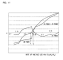
- FIG. 11 shows the quantity of power fluctuation of the DC power sources V 1B and V 2B due to charging and discharging via the inverters, where the horizontal axis represents the rate of voltage use and the vertical axis represents the quantity of power.
- the 1B power and 2B power represent the quantity of power fluctuation of the DC power source V 1B of 1B-INV and the quantity of power fluctuation of the DC power source V 2B of the 2B-INV.
- the sum of these (1B power + 2B power) is also shown.
- the quantity of power fluctuation is positive, the quantity of discharging is larger than the quantity of charging. When it is negative, the quantity of charging is larger.
- the rate of voltage use of the power conditioner Vm/ (V 1B +V 2B +V 3B ) is controlled to be P or Q.
- the quantity of power fluctuation of the DC power sources V 1B and V 2B of the inverters 1B-INV and 2B-INV due to charging and discharging via the inverters can be made substantially zero or minimum. Therefore, the quantity of power provided to the DC power sources V 1B and V 2B from the DC power source V 3B (smoothing capacitor 4) of the inverter 3B-INV via the DC-DC converter 5 can be reduced to the minimum. Therefore, the power loss of the DC-DC converter 5 can be reduced and the efficiency of the power conditioner can be improved.
- the magnitude of (1B power + 2B power) may be minimum if the inverters 1B-INV and 2B-INV have the same output pattern. However, if their output patterns are different, the sum of the absolute value of 1B power and the absolute value of 2B power needs to be calculated to find the case where the quantity of power is minimum. Therefore, the rate of voltage use is controlled to be P or Q in accordance with the output patterns of the inverters 1B-INV and 2B-INV.
- V 3B should be (Vm/P) ⁇ (9/13).
- the voltage value in this case is V mp .
- V mQ (Vm/Q) ⁇ (9/13) should be calculated and the output voltage V 3B of the chopper circuit 3 may be made V mQ .
- FIG. 12 shows the operation voltage with respect to the solar light voltage in the chopper circuit 3 of the power conditioner.
- FIG. 12(a) shows the case where the rate of voltage use of the power conditioner is constantly P.
- V mp the efficiency of the power conditioner can be improved.
- the boosting operation of the chopper circuit 3 is stopped and the power loss of the chopper circuit 3 is significantly reduced, leaving only the continuity power loss of the diode 3c. Also, as the solar light voltage V O increases, the current is lowered and the continuity power loss of the diode 3c is lowered, too. Thus, since the chopper circuit 3 is operated to realize both the reduction in the power loss of the DC-DC converter 5 and the reduction in the power loss of the chopper circuit 3, the overall efficiency of the power conditioner can be improved accurately.
- the rate of voltage use Vm/(V 1B +V 2B +V 3B ) of the power conditioner is controlled to be P or Q.
- the rate of voltage use is controlled to a value close to P or Q, the quantity of power fluctuation of the DC power sources V 1B and V 2B via the inverters can be sufficiently reduced, and the quantity of power fluctuation can be controlled to a predetermined quantity or less.
- the rate of voltage use is controlled within the range of 0.8 to 0.9, the quantity of power fluctuation can be restrained within a predetermined range and the advantage of reduction in the power loss of the DC-DC converter 5 can be provided.
- the ratio of V 1B , V 2B and V 3B is 1:3:9 is described.
- the relation between the rate of voltage use and the quantity of power fluctuation of the DC power source V 1B and V 2B due to charging and discharging via the inverters is similar in the patterns shown in FIG. 4 and FIG. 5, though the operating point of the rate of voltage use is different. Therefore, the similar advantage can be provided if the rate of voltage use is controlled to P or Q to reduce the quantity of power fluctuation of the DC power sources V 1B and V 2B in each case.
- PWM control may additionally be used for each gradational level of the output voltage V A of the inverter unit 1 in the above embodiment. Since there is no change in the average output voltage, the similar advantage can be provided.
- FIG. 13 shows the output voltage waveforms of the inverters 1B-INV, 2B-INV and 3B-INV. As shown in FIG.
- the inverter 1B-INV and the inverter 2B-INV are caused to produce outputs under PWM control in order to compensate for the difference between the target output voltage and the output voltage of the inverter 3B-INV.
- the output of the inverter 1B-INV and the output of the inverter 2B-INV are equal, the quantities of their output power are equal and no power is supplied or received between the DC power sources V 1B and V 2B via the inverters. Therefore, charges are supplied or demanded to the DC-power sources V 1B and V 2B of the inverters 1B-INV and 2B-INV from the DC power source V 3B of the inverter 3B-INV via the DC-DC converter 5.
- the quantity of power supplied to the DC power sources V 1B and V 2B from the DC power source V 3B of the inverter 3B-INV via the DC-DC converter 5 can be minimized, and the power loss of the DC-DC converter 5 can be reduced to the minimum.
- the efficiency of the power conditioner can be improved.
- the two inverters 1B-INV and 2B-INV have the same voltage of the DC power sources V 1B and V 2B and the same output, the configuration of the inverter unit 1 can be simple and easily controlled.
- FIG. 14 is a schematic configuration view showing a power conditioner according to Embodiment 6 of the invention.
- AC sides of plural (in this case, two) single-phase inverters 3B-INV and 2Ba-INV are connected in series to form an inverter unit 1a, which is a single-phase multiple converter.
- DC power sources (first power source and second power source) V 3B and V 2Ba that serve as the inputs of the single-phase inverters 3B-INV and 2Ba-INV are connected to a bidirectional DC-DC converter 5a.
- a chopper circuit 3 as a booster circuit including a switch 3a such as IGBT, a reactor 3b and a diode 3c is installed on the stage subsequent to a DC power source 2 based on solar light, which is a third DC power source.
- the inverter unit 1a outputs a voltage V A that is the sum of the generated voltages combined from the single-phase inverters 3B-INV and 2Ba-INV, under gradational output voltage control operation.
- This output voltage V A is smoothed by a smoothing filter 6 including a reactor 6a and a capacitor 6b, and an AC voltage V out is supplied to the system or load.
- FIG. 15 shows the output voltage waveforms of the inverters 2Ba-INV and 3B-INV.
- the inverter 2Ba-INV is caused to produce an output under PWM control in order to compensate for the difference between the target output voltage and the output voltage of the inverter 3B-INV.
- charges are supplied or demanded to the DC-power sources V 2Ba of the inverter 2Ba-INV from the DC power source V 3B of the inverter 3B-INV via the DC-DC converter 5a.
- the quantity of power supplied or demanded between the DC power source V 2Ba and the DC power source V 3B of the inverter 3B-INV via the DC-DC converter 5a can be minimized, and the power loss of the DC-DC converter 5a can be reduced to the minimum.
- the efficiency of the power conditioner can be improved.
- FIG. 16 is a schematic configuration view showing a power conditioner according to Embodiment 7 of the invention.
- the DC-DC converter 5a can be omitted as shown in FIG. 16 as long as the rate of voltage use can satisfactorily be controlled to P.
- Reference mark 8 represents a capacitor that forms the DC power source V B2a .
- reference marks 8a and 8b represent capacitors that form the DC power sources V 1B and V 2B .
- the efficiency of the power conditioner can be improved and the apparatus configuration can be miniaturized and simplified.
- FIG. 18 is a schematic configuration view showing a power conditioner according to Embodiment 8 of the invention.
- the power conditioner is described in which the DC-DC converter 5 or 5a for supplying and demanding power between the DC power source V 3B and the other DC power sources is omitted.
- a DC-DC converter 5b that supplies power only between the DC power sources V 1B and V 2B may be provided, as shown in FIG. 18.
- the rate of voltage use is satisfactorily controlled to P.
- the supply and demand of power from the DC power source V 3B to the DC power sources V 1B and V 2B is not necessary, and power is supplied and demanded only between the DC power sources V 1B and V 2B via the DC-DC converter 5b.
- V 1B V 2B does not have to hold and the voltage ratio of the DC power sources V 1B , V 2B and V 3B may be, for example, 1:3:9. Also, if there is a point where the sum of the quantities of power fluctuating in the DC power sources V 1B and V 2B due to charging and discharging via the inverters becomes zero (the rate of voltage use P) and the rate of voltage use can be accurately controlled to P, the voltage ratio of the DC power sources V 1B , V 2B and V 3B may be other than 1:3:9. Also, since the DC-DC converter 5b is for supplying and demanding power only between the DC power sources V 1B and V 2B , its power loss is small and the efficiency of the power conditioner can be improved.
- the rate of voltage use Vm/(V 1B +V 2B +V 3B ) of the power conditioner is controlled to be P or Q, thereby causing the quantity of power fluctuating in the DC power sources V 1B and V 2B due to charging and discharging via the inverters to be zero or minimum.
- the quantities of power of the DC power sources V 1B and V 2B are adjusted, as shown in FIG. 19. As shown in FIG.
- Reference mark 15 represents the output pulse of the inverter 3B-INV
- 16 represents the total output from the inverters 1B-INV and 2B-INV
- reference mark 17 represents the AC output voltage V out from the power conditioner.
- Reference marks 15a and 15b represent the output pulse of the inverter 3B-INV before and after the adjustment of the pulse width
- reference marks 16a and 16b represent the total output of the inverters 1B-INV and 2B-INV before and after the adjustment of the pulse width.
- Reference marks 15c and 15d represent the output pulse of the inverter 3B-INV before and after the adjustment of the pulse width
- reference marks 16c and 16d represent the total output of the inverters 1B-INV and 2B-INV before and after the adjustment of the pulse width.
- the power load of the inverters 1B-INV and 2B-INV can be easily adjusted by the increase or decrease of the output pulse width of the inverter 3B-INV. Therefore, the quantity of outflow charges (Q 1B +Q 2B ) from the DC power sources V 1B and V 2B can be easily adjusted to approach zero.
- adjustment can be easily made so that the quantity of power fluctuating in the DC power sources V 1B and V 2B of the inverters 1B-INV and 2B-INV due to charging and discharging via the inverters is reduced. Therefore, the power handled by the DC-DC converter 5 can easily be made closer to zero and the power loss of the DC-DC converter 5 can be reduced.
- the efficiency of the power conditioner can be improved.
- the invention can be broadly applied to an uninterruptible power supply apparatus that boosts a DC voltage of a decentralized power source such as solar light to a required voltage and then converts it to AC and links it to a system, or an inverter apparatus that supplies AC power after conversion to a load.
- a decentralized power source such as solar light
- inverter apparatus that supplies AC power after conversion to a load.
Abstract
Description
- The present invention relates to a power conversion apparatus that converts DC power to AC power, and particularly to a power conversion apparatus used for a power conditioner or the like that links a decentralized power source to a system.
- In a conventional power conditioner, for example, as seen in a solar power conditioner, the voltage from a decentralized power source that is a solar battery is boosted by using a chopper, and a PWM-controlled inverter is inserted onto the subsequent stage, thus generating an output AC voltage.
A basic operation of such a conventional power conditioner will be described hereinafter. DC power outputted from the solar battery drives an internal control power source of the power conditioner and thus enables an internal circuit to operate. The internal circuit has a chopper circuit and an inverter unit. The chopper circuit boosts the voltage of the solar battery to a voltage that is required for linking to the system. The inverter unit includes four switches and carries out PWM switching to form an output current having a phase synchronous with the system voltage. A strip-like waveform is outputted in this manner, and the time ratio for output is changed to control the average voltage of the output. The outputted voltage is averaged by a smoothing filter provided on the output side, and AC power is outputted to the system (see, for example, non-patent reference 1). - Non-patent reference 1: "Development of Solar Power Conditioner Type KP40F", OMRON TECHNICS, Vol.42, No.2 (Serial No.142) 2002
- In the conventional power conditioner, which links a solar light voltage to the system, the maximum value of output voltage of the inverter is decided by the magnitude of the boosted voltage by the chopper. Therefore, for example, in the case of outputting AC power of 200 V, a boosted DC voltage of 282 V or higher is necessary and a higher value is usually set in order to give an allowance. The output voltage of the solar light voltage is usually approximately 200 V or lower, and it needs to be boosted to 282 V or higher as described above. If the boosting rate increases, the power loss of the switching device and diode of the chopper unit increases, and there is a problem that the overall efficiency of the power conditioner is lowered.
- This invention has been made in order to solve the above problems. It is an object of the invention to reduce power loss of each unit and improve conversion efficiency in a power conversion apparatus that converts power from a DC power source such as solar light to AC and outputs AC to a system and load.
- In a first power conversion apparatus according to the invention, AC sides of plural single-phase inverters that convert DC power of DC power sources to AC power are connected in series, and gradational output voltage control operation of an output voltage is carried out by using the sum of generated voltages from a predetermined combination selected from the plural single-phase inverters. The plural DC power sources that serve as inputs of the respective single-phase inverters include a first DC power source having the highest voltage, and another or other plural second DC power sources. Then, the first DC power source is generated by a third DC power source via a booster circuit, and when the voltage of the third DC power source exceeds a predetermined voltage, on-off operation of a switch in the booster circuit is stopped to stop boosting operation.
- Also, in a second power conversion apparatus according to the invention, AC sides of plural single-phase inverters that convert DC power of DC power sources to AC power are connected in series, and gradational output voltage control operation of an output voltage is carried out by using the sum of generated voltages from a predetermined combination selected from the plural single-phase inverters. The plural DC power sources that serve as inputs of the respective single-phase inverters include a first DC power source having the highest voltage, and another or other plural second DC power sources. Then, the first DC power source is generated by a third DC power source via a booster circuit, and an output voltage of the booster circuit is set so that the total quantity of power fluctuation due to charging and discharging of the respective second DC power sources via the respective single-phase inverters is equal to a predetermined quantity or less.
- Moreover, in a third power conversion apparatus according to the invention, AC sides of plural single-phase inverters that convert DC power of DC power sources to AC power are connected in series, and gradational output voltage control operation of an output voltage is carried out by using the sum of generated voltages from a predetermined combination selected from the plural single-phase inverters. The plural DC power sources that serve as inputs of the respective single-phase inverters include a first DC power source having the highest voltage, and another or other plural second DC power sources. Then, the first DC power source is generated by a third DC power source via a booster circuit, and the first DC power source and each of the second DC power sources are connected with each other via a DC-DC converter. The output pulse width of the single-phase inverter that takes the first DC power source as its input is adjusted so that the total quantity of power fluctuation due to charging and discharging of the respective second DC power sources via the respective single-phase inverters is reduced.
- In the first power conversion apparatus according to the invention, a higher output than the output voltage of the booster circuit that boosts the voltage of the third DC power source can be outputted, and the boosting rate of the booster circuit can be reduced, thus reducing the power loss. Also, since on-off operation of the switch in the booster circuit is stopped to stop boosting operation when the voltage of the third DC power source exceeds a predetermined voltage, the power loss due to boosting can be significantly reduced, and a power conversion apparatus with high conversion efficiency can be provided.
- In the second power conversion apparatus according to the invention, a higher output than the output voltage of the booster circuit that boosts the voltage of the third DC power source can be outputted, and the boosting rate of the booster circuit can be reduced, thus reducing the power loss. Also, since the output voltage of the booster circuit is set so that the total quantity of power fluctuation due to charging and discharging of the respective second DC power sources via the respective single-phase inverters is equal to a predetermined quantity or less, the quantity of power provided to the second DC power sources from outside can be restrained and the power loss can be restrained. Therefore, a power conversion apparatus with high conversion efficiency can be provided.
- In the third power conversion apparatus according to the invention, a higher output than the output voltage of the booster circuit that boosts the voltage of the third DC power source can be outputted, and the boosting rate of the booster circuit can be reduced, thus reducing the power loss. Also, since the first DC power source generated via the booster circuit and the respective second DC power sources are connected with each other via the DC-DC converter and the output pulse width of the single-phase inverter that takes the first DC power source as its input is adjusted so that the total quantity of power fluctuation due to charging and discharging of the respective second DC power sources via the respective single-phase inverters is reduced, the quantity of power provided via the DC-DC converter can be restrained by easy adjustment and the power loss can be restrained. Therefore, a power conversion apparatus with high conversion efficiency can be provided.
-
- [FIG. 1] FIG. 1 is a schematic configuration view showing a power conditioner according to
Embodiment 1 of the invention. - [FIG. 2] FIG. 2 is a view showing an output pattern and an output voltage waveform of each single-phase inverter according to
Embodiment 1 of the invention. - [FIG. 3] FIG. 3 is a view showing an output voltage waveform under PWM control of the inverter according to
Embodiment 1 of the invention. - [FIG. 4] FIG. 4 is a view showing the relation between output pattern and output gradational level of each single-phase inverter according to
Embodiment 1 of the invention. - [FIG. 5] FIG. 5 is a view showing DC voltage conditions and output voltage waveform of each single-phase inverter according to
Embodiment 1 of the invention. - [FIG. 6] FIG. 6 is a view showing the operation of a chopper circuit according to
Embodiment 1 of the invention. - [FIG. 7] FIG. 7 is a schematic configuration view showing a power conditioner according to
Embodiment 2 of the invention. - [FIG. 8] FIG. 8 is a view showing the operation of a chopper circuit according to
Embodiment 2 of the invention. - [FIG. 9] FIG. 9 is a view showing the configuration of a bypass circuit according to
Embodiment 3 of the invention. - [FIG. 10] FIG. 10 is a view showing the quantity of charges flowing out via each single-phase inverter according to
Embodiment 4 of the invention. - [FIG. 11] FIG. 11 is a view showing the relation between the quantity of power fluctuation via each single-phase inverter and the rate of voltage use according to
Embodiment 4 of the invention. - [FIG. 12] FIG. 12 is a view showing the operation of a chopper circuit according to
Embodiment 4 of the invention. - [FIG. 13] FIG. 13 is a view showing an output voltage waveform of each single-phase inverter according to
Embodiment 5 of the invention. - [FIG. 14] FIG. 14 is a schematic configuration view showing a power conditioner according to
Embodiment 6 of the invention. - [FIG. 15] FIG. 15 is a view showing an output voltage waveform of each single-phase inverter according to
Embodiment 6 of the invention. - [FIG. 16] FIG. 16 is a schematic configuration view showing a power conditioner according to
Embodiment 7 of the invention. - [FIG. 17] FIG. 17 is a schematic configuration view showing a power conditioner according to another example of
Embodiment 7 of the invention. - [FIG. 18] FIG. 18 is a schematic configuration view showing a power conditioner according to
Embodiment 8 of the invention. - [FIG. 19] FIG. 19 is a view for explaining output pulse adjustment according to
Embodiment 9 of the invention. -
- 2
- third DC power source (solar light)
- 3
- chopper circuit as booster circuit
- 3a
- switch
- 4
- smoothing capacitor as first DC power source
- 5, 5a, 5b
- DC-DC converter
- 7
- bypass circuit
- 7a
- relay
- 8, 8a, 8b
- capacitor as second DC power source
- 15, 15a to 15d
- output pulse
- 17
- output voltage
- 1B-INV, 2B-INV, 2Ba-INV, 3B-INV
- single-phase inverter
- Q1B+Q2B
- quantity of charges
- Hereinafter, a power conversion apparatus (hereinafter referred to as power conditioner) according to
Embodiment 1 of the invention will be described with reference to the drawings.
FIG. 1 is a schematic configuration view showing a power conditioner according toEmbodiment 1 of the invention. As shown in FIG. 1(a), AC sides of plural (in this case, three) single-phase inverters 3B-INV, 2B-INV and 1B-INV are connected in series to form aninverter unit 1, which is a single-phase multiple converter. Also, achopper circuit 3 as a booster circuit including a switching device (hereinafter referred to as switch) 3a such as IGBT,reactor 3b and adiode 3c is installed on a stage subsequent to aDC power source 2 based on solar light as a third DC power source. Thechopper circuit 3 boosts a DC voltage VO acquired at theDC power source 2 and thus provides a voltage VC charging a smoothingcapacitor 4, which serves as a first DC power source. - Each of the single-
phase inverters 3B-INV, 2B-INV and 1B-INV includes plural self-turn-off semiconductor switching devices such as IGBTs with diodes connected in inverse-parallel, as shown in FIG. 1(b). They convert DC power to AC power and output it. The DC power sources of the inputs of them are connected with one another via a bidirectional DC-DC converter 5.
These single-phase inverters 3B-INV, 2B-INV and 1B-INV can generate positive, negative and zero voltages. Theinverter unit 1 outputs a voltage VA as the sum of these generated voltages combined, by gradational output voltage control operation. This output voltage VA is smoothed by a smoothingfilter 6 including areactor 6a and acapacitor 6b and an AC voltage Vout is supplied to a system or load. - Also, the DC power source (first DC power source) that serves as the input of 3B-INV is equivalent to the smoothing
capacitor 4. Its voltage V3B(=VC) is larger than voltages V2B, V1B of the DC power sources (second DC power sources) that serve as the inputs of the other single-phase inverters 2B-INV and 1B-INV. V3B, V2B and V1B are controlled to have a predetermined voltage ratio by the DC-DC converter 5. This DC-DC converter 5 keeps a constant voltage ratio of the DC power sources V1B, V2B and V3B of the respective inverters and allows them to supply excess energy to compensate for insufficiency among them.
Since V1B, V2B and V3B represent the DC power source voltages of theinverters 1B-INV, 2B-INV and 3B-INV, hereinafter, the DC power sources that serve as the inputs of the inverters are described as the DC power source V1B, the DC power source V2B and the DC power source V3B, for convenience.
It is now assumed that the relation between V1B, V2B and V3B is 1:3:9. In this case, when output patterns of the threeinverters 1B-INV, 2B-INV and 3B-INV are combined well, as shown in FIG. 2(a), output voltages of 14gradational levels 0 to 13 can be selected as the output voltage VA of theinverter unit 1. Thus, as shown in FIG. 2(b), the output voltage VA that has a substantially sine wave-likeoutput voltage waveform 11 is provided and it is inputted to the smoothingfilter 6. Moreover, if PWM control is used, too, in each gradational level, the voltage waveform can be controlled more accurately, as shown in FIG. 3. In the output patterns of each inverter shown in FIG. 2(a), 1 represents generation of a positive voltage, -1 represents generation of a negative voltage, and 0 represents generation of zero voltage. - The relation between V1B, V2B and V3B may be other than 1:3:9. With various patterns from 1 : 2 : 4 to 1:3:9, the output voltage VA can be continuously changed in the gradational level. Logic tables A to J in FIG. 4 show the relation between the output patterns of the
inverters 1B-INV, 2B-INV and 3B-INV and the gradational levels of the output voltage VA of theinverter unit 1 having these inverters connected in series, for each pattern. For the case of 1:3:9 of these, the number of levels is the largest and a highly accurate output voltage waveform can be expected. If PWM control is used, too, in each gradational level, the voltage waveform can be controlled more accurately. To apply PWM to the voltage output method on each gradational level, it may be necessary to apply PWM control to the outputs of plural single-phase inverters, depending on the relation of the voltages V1B, V2B and V3B. - In the case where the use of PWM control is assumed, the voltage of the DC power source V1B may be larger than the value in the relation shown in FIG. 4. Since there is an overlap of ΔV between gradational levels as shown in FIG. 5(a) in addition to the voltage control based on PWM control, more continuous waveform outputs can be made. Conditions Ax to Jx corresponding to the logic tables A to J in FIG. 4 are shown in FIG. 5(b). For example, under the condition Jx, ΔV=V1B-V3B/9 holds.
- Meanwhile, the maximum output voltage necessary for an AC output of 200 V is approximately 282 V. The output voltage VA of the
inverter unit 1 can be V1B+V2B+V3B at the maximum. Therefore, if V1B+V2B+V3B is equal to 282 V or higher, the power conditioner can provide an AC output of 200 V. V1B+V2B+V3B is larger than V3B, which is the voltage boosted by thechopper circuit 3. For example, if the relation between V1B, V2B and V3B is 1:3:9, V1B+V2B+V3B is 13/9 times V3B. That is, when V3B is about 195 V or higher, V1B+V2B+V3B is 282 V or higher and this is the condition for an AC output.
FIG. 6 shows an operation voltage with respect to a solar light voltage in thechopper circuit 3 of such a power conditioner and an estimate efficiency value at the time. As shown in FIG. 6, the DC voltage (solar light voltage) VO acquired at theDC power source 2 is boosted to a predetermined voltage Vm1 as theIGBT switch 3a turns on and off up to the predetermined voltage Vm1 (195 V). When the predetermined voltage Vm1 is exceeded, theIGBT switch 3a is stopped. - In this manner, if the solar light voltage VO is 195 V or higher, a predetermined AC output can be provided without the boosting operation. Therefore, the boosting operation by the
chopper circuit 3 is stopped at this time. As the solar light voltage VO increases, the boosting rate is lowered and the efficiency of thechopper circuit 3 improves. However, when theIGBT switch 3a is stopped, the power loss is significantly reduced and there is only a continuity power loss of thediode 3c. Therefore, the efficiency suddenly increases from the point where the solar light voltage VO reaches 195 V. As it rises further above 195 V, the increase in the solar light voltage VO causes the current to be lowered and the continuity power loss in thediode 3c is reduced (under the same power condition). Therefore, the overall efficiency of the power conditioner increases. - In this embodiment, the AC side of the single-
phase inverter 3B-INV using, as its DC source, the DC voltage V3B boosted from the solar light voltage VO by thechopper circuit 3, and of the other single-phase inverters 2B-INV and 1B-INV are connected in series, and the power conditioner is thus configured to provide an output voltage based on the sum of the generated voltages from the respective inverters. Therefore, a higher voltage than the DC voltage V3B boosted by thechopper circuit 3 can be outputted, and the boosting rate of thechopper circuit 3 can be reduced, thus reducing the power loss. Also, when a voltage range lower than the maximum value of the output voltage of the power conditioner is employed as the operation range of the voltage V3B, the boosting rate of thechopper circuit 3 can be securely reduced and the power loss can be reduced. Moreover, when the solar light voltage VO exceeds a predetermined voltage Vm1 (195 V), theIGBT switch 3a is stopped to stop the boosting operation. Therefore, the power loss due to boosting can be significantly reduced as described above, and a power conditioner with high conversion efficiency can be provided. - FIG. 7 is a schematic configuration view showing a power conditioner according to
Embodiment 2 of the invention. The power conditioner according to this embodiment is configured by providing abypass circuit 7 that bypasses thechopper circuit 3 in the power conditioner shown in FIG. 1 of theabove Embodiment 1.
As shown in FIG. 7, thechopper circuit 3 boosts a DC voltage VO acquired at theDC power source 2, and a voltage VC to charge the smoothingcapacitor 4, which serves as the first power source, is provided. Also, to bypass thechopper circuit 3 while stopping the boosting, thebypass circuit 7 including, for example, arelay 7a, is connected parallel to thechopper circuit 3. - As in the
above Embodiment 1, the single-phase inverters 3B-INV, 2B-INV and 1B-INV can generate positive, negative and zero voltages as their outputs. Theinverter unit 1 outputs a voltage VA as the sum of these generated voltages combined, by gradational output voltage control operation. This output voltage VA is smoothed by the smoothingfilter 6 including thereactor 6a and thecapacitor 6b, and an AC voltage Vout is supplied to the system or load.
The operation of the power conditioner in the case where the relation between the DC power sources V1B, V2B and V3B of theinverters 1B-INV, 2B-INV and 3B-INV is 1:3:9 will be described hereinafter.
As described above, the maximum output voltage necessary for an AC output of 200 V is approximately 282 V, and the output voltage VA of theinverter unit 1 can be V1B+V2B+V3B at maximum. Therefore, in order to acquire a predetermined AC output Vout in the case where the relation between V1B, V2B and V3B is 1:3:9, thechopper circuit 3 must be operated to keep V3B around 195 V or higher. - In the
chopper circuit 3, theIGBT switch 3a is turned on and off until the DC voltage (solar light voltage) VO acquired at theDC power source 2, which serves as its input, reaches a predetermined voltage Vm1 (195 V), and it is thus boosted to the voltage Vm1. During this time, therelay 7a of thebypass circuit 7 is left open. Then, theIGBT switch 3a is stopped when the predetermined voltage Vm1 is exceeded. At this point, therelay 7a of thebypass circuit 7 is closed and a current is caused to flow to the side of thebypass circuit 7, thus bypassing thereactor 3b and thediode 3c of thechopper circuit 3. - FIG. 8 shows an operation voltage with respect to the solar light voltage VO in the
chopper circuit 3 and an estimate efficiency value at the time.
As shown in FIG. 8, in the range where the solar light voltage VO is equal to or less than the predetermined voltage Vm1, thechopper circuit 3 carries out boosting so that the output voltage V3B becomes the predetermined voltage Vm1. Therefore, as the solar light voltage VO increases, the boosting rate is lowered and the efficiency of thechopper circuit 3 improves. When the solar light voltage VO exceeds the predetermined voltage Vm1, the boosting operation stops and therelay 7a of thebypass circuit 7 is closed to cause a current to flow to the side of thebypass circuit 7. Therefore, there is little power loss. Thus, the efficiency of the chopper circuit suddenly increases from the point where the solar light voltage VO reaches the voltage Vm1. - The predetermined voltage Vm1 at which the boosting operation should be stopped may be approximately 195 V or higher. However, a lower voltage enables further reduction in the power loss of the
chopper circuit 3. After the boosting operation is stopped, not only the power loss can be significantly reduced by the stop of theIGBT switch 3a, but also the continuity power loss of thereactor 3b and thediode 3c can be eliminated by bypassing thereactor 3b and thediode 3c in thechopper circuit 3. There is almost no power loss in thechopper circuit 3. Therefore, a power conditioner with high conversion efficiency can be provided. - The
bypass circuit 7 in theabove Embodiment 2 will be described in detail hereinafter.
Thebypass circuit 7 includes therelay 7a and bypasses one or both of thereactor 3b and thediode 3c connected in series in thechopper circuit 3.
In FIG. 9(a), therelay 7a bypasses thereactor 3b and thediode 3c, as described in theabove Embodiment 2. In FIG. 9 (b), therelay 7a bypasses only thediode 3c. In FIG. 9(c), therelay 7a bypasses only thereactor 3b.
Also, a self-turn-offsemiconductor switch 7b is connected parallel to therelay 7a. Since therelay 7a usually opens with zero current or a low voltage, a DC current is difficult to interrupt. However, it can be easily interrupted when thesemiconductor switch 7b is thus provided in parallel. In this case, thesemiconductor 7b is turned on at the same time as therelay 7a is opened, and the current is temporarily shifted to thesemiconductor switch 7b. Thus, the current flowing through therelay 7a is interrupted, and thesemiconductor switch 7b is turned off after that. - In any case, when the solar light voltage VO exceeds the predetermined voltage Vm1, the
IGBT switch 3a is stopped to stop the boosting operation, and therelay 7a of thebypass circuit 7 is closed to cause the current to flow to the side of thebypass circuit 7.
In the case of FIG. 9(a), since thereactor 3b and thediode 3c in thechopper circuit 3 are bypassed, the continuity power loss of thereactor 3b and thediode 3c can be eliminated and the overall efficiency of the power conditioner increases.
In the case of FIG. 9(b), since only thediode 3c in thechopper circuit 3 is bypassed, the continuity power loss of thediode 3c can be eliminated and the overall efficiency of the power conditioner increases. In this case, since thereactor 3b is not bypassed, thereactor 3b can be used as a filter. - In FIG. 9(a) and FIG. 9(b), since the
diode 3c is bypassed, when the DC power source V3B gets higher than the solar light voltage Vo, reversal of the current occurs, and additionally, a reverse voltage is applied to the solar panel, which is theDC power source 2. There is a risk of damage to the panel. Therefore, a configuration is made that detects the current flowing through therelay 7a, and that opens therelay 7a when the current becomes a predetermined value or less, in order to switch to the current path via thereactor 3b and thediode 3c. As therelay 7a is thus opened to make the function of thediode 3c effective, the functions of preventing reversal of the current and of protecting the solar panel from the reverse voltage are provided.
When therelay 7a is opened, even if a reverse current has already been generated because of delay in detection, the current can be temporarily shifted to thesemiconductor switch 7b and thus can be securely interrupted. - In the case of FIG. 9(c), since only the
reactor 3b in thechopper circuit 3 is bypassed, the continuity power loss of thereactor 3b can be eliminated and the overall efficiency of the power conditioner increases. Also, since thediode 3c is not bypassed, reversal of the current can be prevented and the solar panel can be protected from the reverse voltage by thediode 3c, and reliability can be easily improved. In this case, therelay 7a can be shut off without having thesemiconductor switch 7b provided. However, as thesemiconductor switch 7b is provided, therelay 7a can also be shut off when anomaly occurs in thediode 3c. - Next, improvement in the efficiency of the DC-
DC converter 5 in the power conditioner having the similar circuit configuration shown in FIG. 1 of theabove Embodiment 1 will be described hereinafter.
As shown in FIG. 1, the DC power sources V1B, V2B and V3B that serve as the inputs of theinverters 1B-INV, 2B-INV and 3B-INV are connected by the bidirectional DC-DC converter 5. This DC-DC converter 5 keeps the voltage ratio of the DC power sources V1B, V2B and V3B of the inverters at a constant value and also allows them to supply excess energy to compensate for insufficiency among them. - Here, it is assumed that the maximum value (peak value) of the AC voltage Vout outputted from the power conditioner is Vm, and that the rate of voltage use is Vm/(V1B+V2B+V3B). The relation between this rate of voltage use and the quantity of power fluctuation of the DC power sources V1B, V2B and V3B due to charging and discharging via the inverters will be described hereinafter.
FIG. 10 shows the quantity of charges that flow out via the inverters in the case where the voltage ratio of the DC power sources V1B, V2B and V3B of the inverters is 1: 3: 9 and when a sine-wave current with a power factor of 1 is caused to flow through a load connected to the power conditioner, with respect to the rate of voltage use of 1 and 0.85. In FIG. 10, the 1B quantity of charges, 2B quantity of charges and 3B quantity of charges represent the quantities of charges that have flowed out from the DC power sources V1B, V2B and V3B because of charging and discharging via theinverters 1B-INV, 2B-INV and 3B-INV.
As shown in FIG. 10(a) and FIG. 10(b), the quantities of charges that flow out from the DC power sources V1B and V2B via the inverters are much smaller for the rate of voltage use of 0.85 than for 1. - FIG. 11 shows the quantity of power fluctuation of the DC power sources V1B and V2B due to charging and discharging via the inverters, where the horizontal axis represents the rate of voltage use and the vertical axis represents the quantity of power. The 1B power and 2B power represent the quantity of power fluctuation of the DC power source V1B of 1B-INV and the quantity of power fluctuation of the DC power source V2B of the 2B-INV. The sum of these (1B power + 2B power) is also shown. When the quantity of power fluctuation is positive, the quantity of discharging is larger than the quantity of charging. When it is negative, the quantity of charging is larger.
As shown in FIG. 11, (1B power + 2B power) is zero when the rate of voltage use is P (= about 0.83). Also, the sum of the absolute value of 1B power and the absolute value of 2B power is minimum when the rate of voltage use is Q (= about 0.845). - According to the above characteristics, in this embodiment, the rate of voltage use of the power conditioner = Vm/ (V1B+V2B+V3B) is controlled to be P or Q. Thus, the quantity of power fluctuation of the DC power sources V1B and V2B of the
inverters 1B-INV and 2B-INV due to charging and discharging via the inverters can be made substantially zero or minimum. Therefore, the quantity of power provided to the DC power sources V1B and V2B from the DC power source V3B (smoothing capacitor 4) of theinverter 3B-INV via the DC-DC converter 5 can be reduced to the minimum. Therefore, the power loss of the DC-DC converter 5 can be reduced and the efficiency of the power conditioner can be improved. - To minimize the quantity of power provided to the DC power sources V1B and V2B from the DC power source V3B (smoothing capacitor 4) via the DC-
DC converter 5, the magnitude of (1B power + 2B power) may be minimum if theinverters 1B-INV and 2B-INV have the same output pattern. However, if their output patterns are different, the sum of the absolute value of 1B power and the absolute value of 2B power needs to be calculated to find the case where the quantity of power is minimum. Therefore, the rate of voltage use is controlled to be P or Q in accordance with the output patterns of theinverters 1B-INV and 2B-INV. - To achieve the rate of voltage use of P in the power conditioner, for example, when the ratio of V1B, V2B and V3B is 1:3:9, V3B should be (Vm/P)×(9/13). The voltage value in this case is Vmp. For the AC voltage Vout of 200 V, Vm is about 282 V and P is about 0.83. Therefore, Vmp is about 235 V.
Therefore, as the DC voltage V3B boosted from the solar light voltage VO by thechopper circuit 3 is made Vmp (= about 235 V), the rate of the voltage use of the power conditioner can be controlled to P.
Also to control the rate of voltage use to Q, similarly, VmQ = (Vm/Q)×(9/13) should be calculated and the output voltage V3B of thechopper circuit 3 may be made VmQ. - Next, FIG. 12 shows the operation voltage with respect to the solar light voltage in the
chopper circuit 3 of the power conditioner.
FIG. 12(a) shows the case where the rate of voltage use of the power conditioner is constantly P. TheIGBT switch 3a continues the on-off operation and the DC voltage (solar light voltage) VO acquired at theDC power source 2 is constantly boosted to Vmp (= about 235 V). Thus, the power loss of the DC-DC converter 5 can be constantly reduced and the efficiency of the power conditioner can be improved. - In FIG. 10(b), when boosting is necessary for providing a predetermined AC output, that is, when the solar light voltage VO is the voltage Vm1 (195 V) or less described in the
above Embodiment 1, theIGBT switch 3a is turned on and off to boost the solar light voltage VO to Vmp (= about 235 V). Then, when the solar light voltage VO has exceeded the voltage Vm1, theIGBT switch 3a is stopped.
In this manner, under the condition when boosting is necessary, the voltage is boosted to a voltage that enables reduction in the power loss of the DC-DC converter 5, and in the case where a predetermined AC output can be provided without the boosting operation, the boosting operation of thechopper circuit 3 is stopped and the power loss of thechopper circuit 3 is significantly reduced, leaving only the continuity power loss of thediode 3c. Also, as the solar light voltage VO increases, the current is lowered and the continuity power loss of thediode 3c is lowered, too. Thus, since thechopper circuit 3 is operated to realize both the reduction in the power loss of the DC-DC converter 5 and the reduction in the power loss of thechopper circuit 3, the overall efficiency of the power conditioner can be improved accurately. - In the above embodiment, the rate of voltage use = Vm/(V1B+V2B+V3B) of the power conditioner is controlled to be P or Q. However, as the rate of voltage use is controlled to a value close to P or Q, the quantity of power fluctuation of the DC power sources V1B and V2B via the inverters can be sufficiently reduced, and the quantity of power fluctuation can be controlled to a predetermined quantity or less.
Also, as shown in FIG. 11, if the rate of voltage use is controlled within the range of 0.8 to 0.9, the quantity of power fluctuation can be restrained within a predetermined range and the advantage of reduction in the power loss of the DC-DC converter 5 can be provided. - Also, in the above embodiment, the case where the ratio of V1B, V2B and V3B is 1:3:9 is described. However, the relation between the rate of voltage use and the quantity of power fluctuation of the DC power source V1B and V2B due to charging and discharging via the inverters is similar in the patterns shown in FIG. 4 and FIG. 5, though the operating point of the rate of voltage use is different. Therefore, the similar advantage can be provided if the rate of voltage use is controlled to P or Q to reduce the quantity of power fluctuation of the DC power sources V1B and V2B in each case.
- Moreover, PWM control may additionally be used for each gradational level of the output voltage VA of the
inverter unit 1 in the above embodiment. Since there is no change in the average output voltage, the similar advantage can be provided. - Next, a case where the relation between the voltages of the DC power sources V1B, V2B and V3B of the inverters is V1B = V2B ≥ (2/9)×V3B in the power conditioner having the similar circuit configuration shown in FIG. 1 of the
above Embodiment 1, will be described. That is, the voltages of the DC power sources V1B and V2B of theinverters 1B-INV and 2B-INV are equal and the total of these two is equal to or larger than (4/9)×V3B.
FIG. 13 shows the output voltage waveforms of theinverters 1B-INV, 2B-INV and 3B-INV. As shown in FIG. 13, theinverter 1B-INV and theinverter 2B-INV are caused to produce outputs under PWM control in order to compensate for the difference between the target output voltage and the output voltage of theinverter 3B-INV. In this case since the output of theinverter 1B-INV and the output of theinverter 2B-INV are equal, the quantities of their output power are equal and no power is supplied or received between the DC power sources V1B and V2B via the inverters. Therefore, charges are supplied or demanded to the DC-power sources V1B and V2B of theinverters 1B-INV and 2B-INV from the DC power source V3B of theinverter 3B-INV via the DC-DC converter 5. - Also, the
chopper circuit 3 that boosts the solar light voltage VO is caused to operate with the output voltage V3B being Vmp (=(Vm/P)×9/13)), and the rate of voltage use is set at P as shown in FIG. 11 to perform control so that the sum (1B power + 2B power) of the quantities of power fluctuating in the DC power sources V1B and V2B due to charging and discharging via the inverters becomes zero. Thus, the quantity of power supplied to the DC power sources V1B and V2B from the DC power source V3B of theinverter 3B-INV via the DC-DC converter 5 can be minimized, and the power loss of the DC-DC converter 5 can be reduced to the minimum. The efficiency of the power conditioner can be improved. Also, since the twoinverters 1B-INV and 2B-INV have the same voltage of the DC power sources V1B and V2B and the same output, the configuration of theinverter unit 1 can be simple and easily controlled. - Next, a power conditioner according to
Embodiment 6 of the invention will be described with reference to the drawings.
FIG. 14 is a schematic configuration view showing a power conditioner according toEmbodiment 6 of the invention. As shown in FIG. 14, AC sides of plural (in this case, two) single-phase inverters 3B-INV and 2Ba-INV are connected in series to form aninverter unit 1a, which is a single-phase multiple converter. Also, DC power sources (first power source and second power source) V3B and V2Ba that serve as the inputs of the single-phase inverters 3B-INV and 2Ba-INV are connected to a bidirectional DC-DC converter 5a.
Also, achopper circuit 3 as a booster circuit including aswitch 3a such as IGBT, areactor 3b and adiode 3c is installed on the stage subsequent to aDC power source 2 based on solar light, which is a third DC power source. Thechopper circuit 3 boosts a DC voltage VO acquired at theDC power source 2, and a voltage VC (=V3B) to charge a smoothingcapacitor 4, which serves as the first DC power source, is provided. Theinverter unit 1a outputs a voltage VA that is the sum of the generated voltages combined from the single-phase inverters 3B-INV and 2Ba-INV, under gradational output voltage control operation. This output voltage VA is smoothed by a smoothingfilter 6 including areactor 6a and acapacitor 6b, and an AC voltage Vout is supplied to the system or load. - In the power conditioner configured in this manner, it is assumed that the relation between the voltages of the DC power sources V1B and V2Ba of the inverters is V2Ba ≥ (4/9)×V3B.
FIG. 15 shows the output voltage waveforms of the inverters 2Ba-INV and 3B-INV. As shown in FIG. 15, the inverter 2Ba-INV is caused to produce an output under PWM control in order to compensate for the difference between the target output voltage and the output voltage of theinverter 3B-INV. In this case, charges are supplied or demanded to the DC-power sources V2Ba of the inverter 2Ba-INV from the DC power source V3B of theinverter 3B-INV via the DC-DC converter 5a. - Also, the
chopper circuit 3 that boosts the solar light voltage VO is caused to operate with the output voltage V3B being Vmp (=(Vm/P)×9/13)), and the rate of voltage use is set at P as shown in FIG. 11 to perform control so that the quantity of power fluctuating in the DC power source V2Ba due to charging and discharging via each inverter becomes zero. Thus, the quantity of power supplied or demanded between the DC power source V2Ba and the DC power source V3B of theinverter 3B-INV via the DC-DC converter 5a can be minimized, and the power loss of the DC-DC converter 5a can be reduced to the minimum. The efficiency of the power conditioner can be improved. - FIG. 16 is a schematic configuration view showing a power conditioner according to
Embodiment 7 of the invention. In theabove Embodiment 6, charges are supplied or demanded to the DC power source V2Ba of the inverter 2Ba-INV from the DC power source V3B of theinverter 3B-INV via the DC-DC converter 5a. However, the DC-DC converter 5a can be omitted as shown in FIG. 16 as long as the rate of voltage use can satisfactorily be controlled to P. Here,Reference mark 8 represents a capacitor that forms the DC power source VB2a.
That is, when the quantity of power fluctuating in the DC power source V2Ba due to charging and discharging via each inverter can be accurately controlled to be zero, supply and demand of power between the DC power source V2Ba and the DC power source V3B via the DC-DC converter 5a is not necessary, and the power conditioner that does not have the DC-DC converter 5a can be used. Thus, the efficiency of the power conditioner can be improved and the apparatus configuration can be miniaturized and simplified. - The same can apply to the case described in the
above Embodiment 5. As long as the rate of voltage use can be satisfactorily controlled to P, the DC-DC converter 5 can be omitted as shown in FIG. 17. Here, reference marks 8a and 8b represent capacitors that form the DC power sources V1B and V2B. Thus, similarly, the efficiency of the power conditioner can be improved and the apparatus configuration can be miniaturized and simplified. - FIG. 18 is a schematic configuration view showing a power conditioner according to
Embodiment 8 of the invention. In theabove Embodiment 7, the power conditioner is described in which the DC-DC converter DC converter 5b that supplies power only between the DC power sources V1B and V2B may be provided, as shown in FIG. 18.
Theinverter unit 1 is configured similarly to theabove Embodiment 5, and the relation between the voltages of the DC power sources V1B, V2B and V3B of the inverters is V1B = V2B ≥ (2/9)×V3B. The rate of voltage use is satisfactorily controlled to P. In this case, the supply and demand of power from the DC power source V3B to the DC power sources V1B and V2B is not necessary, and power is supplied and demanded only between the DC power sources V1B and V2B via the DC-DC converter 5b. - As the DC-
DC converter 5b that supplies power only between the DC power sources V1B and V2B in this manner is provided, V1B=V2B does not have to hold and the voltage ratio of the DC power sources V1B, V2B and V3B may be, for example, 1:3:9. Also, if there is a point where the sum of the quantities of power fluctuating in the DC power sources V1B and V2B due to charging and discharging via the inverters becomes zero (the rate of voltage use P) and the rate of voltage use can be accurately controlled to P, the voltage ratio of the DC power sources V1B, V2B and V3B may be other than 1:3:9.
Also, since the DC-DC converter 5b is for supplying and demanding power only between the DC power sources V1B and V2B, its power loss is small and the efficiency of the power conditioner can be improved. - In the
above Embodiments 4 to 8, the rate of voltage use Vm/(V1B+V2B+V3B) of the power conditioner is controlled to be P or Q, thereby causing the quantity of power fluctuating in the DC power sources V1B and V2B due to charging and discharging via the inverters to be zero or minimum. However, in this embodiment, by adjusting the output pulse width of theinverter 3B-INV, the quantities of power of the DC power sources V1B and V2B are adjusted, as shown in FIG. 19.
As shown in FIG. 19(a), when the output voltage Vc (V3B) of thechopper circuit 3 of the power conditioner is about 235 V, the rate of voltage use is P (= about 0.83) and the quantity of outflow charges (Q1B+Q2B) from the DC power sources V1B and V2B is close to zero.Reference mark 15 represents the output pulse of theinverter 3B-INV, 16 represents the total output from theinverters 1B-INV and 2B-INV, andreference mark 17 represents the AC output voltage Vout from the power conditioner.
Next, as shown in FIG. 19(b), when the voltage of solar light is lowered by a rise in the ambient temperature or the like and the output voltage Vc (V3B) of thechopper circuit 3 of the power conditioner is, for example, about 204 V, the rate of voltage use is about 0.95 and the quantity of outflow charges (Q1B+Q2B) from the DC power sources V1B and V2B increases. In such a case, if the output pulse width of theinverter 3B-INV is increased, the power load of theinverters 1B-INV and 2B-INV is reduced and (Q1B+Q2B) becomes closer to zero. Reference marks 15a and 15b represent the output pulse of theinverter 3B-INV before and after the adjustment of the pulse width, andreference marks inverters 1B-INV and 2B-INV before and after the adjustment of the pulse width. - Next, as shown in FIG. 19(c), when the voltage of solar light rises because of a drop in the ambient temperature or the like and the output voltage Vc (V3B) of the
chopper circuit 3 of the power conditioner is, for example, about 260 V, the rate of voltage use is about 0.75 and the quantity of outflow charges (Q1B+Q2B) from the DC power sources V1B and V2B decreases, and increases in the negative direction. In such a case, if the output pulse width of theinverter 3B-INV is narrowed, the power load of theinverters 1B-INV and 2B-INV increases and (Q1B+Q2B) becomes closer to zero. Reference marks 15c and 15d represent the output pulse of theinverter 3B-INV before and after the adjustment of the pulse width, andreference marks inverters 1B-INV and 2B-INV before and after the adjustment of the pulse width. - In this manner, the power load of the
inverters 1B-INV and 2B-INV can be easily adjusted by the increase or decrease of the output pulse width of theinverter 3B-INV. Therefore, the quantity of outflow charges (Q1B+Q2B) from the DC power sources V1B and V2B can be easily adjusted to approach zero.
Thus, adjustment can be easily made so that the quantity of power fluctuating in the DC power sources V1B and V2B of theinverters 1B-INV and 2B-INV due to charging and discharging via the inverters is reduced. Therefore, the power handled by the DC-DC converter 5 can easily be made closer to zero and the power loss of the DC-DC converter 5 can be reduced. The efficiency of the power conditioner can be improved.
Also in this case, as in theabove Embodiment 1, when the solar light voltage VO exceeds a predetermined voltage Vm1 (195 V), as theIGBT switch 3a is stopped to stop the boosting operation, the power loss due to the boosting can be significantly reduced as described above, and a power conditioner with higher conversion efficiency can be provided. - The invention can be broadly applied to an uninterruptible power supply apparatus that boosts a DC voltage of a decentralized power source such as solar light to a required voltage and then converts it to AC and links it to a system, or an inverter apparatus that supplies AC power after conversion to a load.
Claims (32)
- A power conversion apparatus in which AC sides of plural single-phase inverters that convert DC power of DC power sources to AC power are connected in series, and in which gradational output voltage control operation of an output voltage is carried out by using the sum of generated voltages from a predetermined combination selected from the plural single-phase inverters, the apparatus being characterized in that
the plural DC power sources that serve as inputs of the respective single-phase inverters include a first DC power source having the highest voltage, and another or other plural second DC power sources, and
the first DC power source is generated by a third DC power source via a booster circuit, and when the voltage of the third DC power source exceeds a predetermined voltage, on-off operation of a switch in the booster circuit is stopped to stop boosting operation. - The power conversion apparatus according to claim 1, comprising a bypass circuit that bypasses the booster circuit,
the apparatus being characterized in that when the voltage of the third DC power source exceeds a predetermined voltage, the on-off operation of the switch in the booster circuit is stopped to stop the boosting operation, and the booster circuit is bypassed by the bypass circuit. - The power conversion apparatus according to claim 2, characterized in that the booster circuit is formed by a series circuit including a reactor and a rectifying device that are connected in series, and the switch having its one end connected to a connection point between the reactor and the rectifying device, and at least the rectifying device in the series circuit is bypassed by the bypass circuit.
- The power conversion apparatus according to claim 3, characterized in that when a current flowing through the bypass circuit has a predetermined value or less, the bypass circuit is shut off and the current is switched to a current path via the booster circuit with its boosting operation stopped.
- The power conversion apparatus according to claim 2, characterized in that the booster circuit is formed by a series circuit including a reactor and a rectifying device that are connected in series, and the switch having its one end connected to a connection point between the reactor and the rectifying device, and only the reactor in the series circuit is bypassed by the bypass circuit.
- The power conversion apparatus according to claim 2, characterized in that the bypass circuit is formed by a relay.
- The power conversion apparatus according to claim 1, characterized in that the first DC power source and the respective second DC power sources are connected via a DC-DC converter.
- The power conversion apparatus according to claim 1, characterized in that the voltage of the first DC power source operates in a lower voltage range than the maximum value of output voltage of the power conversion apparatus.
- The power conversion apparatus according to claim 1, characterized in that second DC power sources are two DC power sources having substantially equal DC voltages.
- The power conversion apparatus according to claim 1, characterized in that the sum of the DC voltages of the respective second DC power sources is equal to or larger than 4/9 of the DC voltage of the first DC power source.
- The power conversion apparatus according to claim 1, characterized in that the output voltage of a predetermined single-phase inverter of the plural single-phase inverters is PWM-controlled, and the PWM-controlled output voltage combined with each output voltage level in the gradational output voltage control operation.
- The power conversion apparatus according to claim 1, characterized in that a predetermined AC voltage and AC current is outputted and supplied to a load, or the predetermined AC output is connected parallel to a system, and the third DC power source is linked to the system.
- A power conversion apparatus in which AC sides of plural single-phase inverters that convert DC power of DC power sources to AC power are connected in series, and in which gradational output voltage control operation of an output voltage is carried out by using the sum of generated voltages from a predetermined combination selected from the plural single-phase inverters, the apparatus being characterized in that
the plural DC power sources that serve as inputs of the respective single-phase inverters include a first DC power source having the highest voltage, and another or other plural second DC power sources,
the first DC power source is generated by a third DC power source via a booster circuit, and
an output voltage of the booster circuit is set so that the total quantity of power fluctuation due to charging and discharging of the respective second DC power sources via the respective single-phase inverters is equal to a predetermined quantity or less. - The power conversion apparatus according to claim 13, characterized in that the first DC power source and the respective second DC power sources are connected via a DC-DC converter.
- The power conversion apparatus according to claim 13, characterized in that the output voltage of the booster circuit is set so that the total quantity of power fluctuation in the respective second DC power sources due to charging and discharging via the respective single-phase inverters is substantially zero.
- The power conversion apparatus according to claim 15, characterized in that the respective second DC power sources are connected with each other via a DC-DC converter.
- The power conversion apparatus according to claim 13, characterized in that a peak value of the output voltage of the power conversion apparatus divided by the sum of the DC voltages of the first and second DC power sources, is controlled within the range of 0.8 to 0.9.
- The power conversion apparatus according to claim 13, characterized in that the total quantity of power fluctuation in the respective second DC power sources via the respective single-phase inverters is the sum of the respective quantities of power fluctuation in the respective second DC power sources or the sum of absolute value of the respective quantities of power fluctuation.
- The power conversion apparatus according to claim 13, characterized in that when the voltage of the third DC power source exceeds a predetermined voltage, on-off operation of a switch in the booster circuit is stopped to stop boosting operation.
- The power conversion apparatus according to claim 13, characterized in that the voltage of the first DC power source operates in a lower voltage range than the maximum value of output voltage of the power conversion apparatus.
- The power conversion apparatus according to claim 13, characterized in that the second DC power sources are two DC power sources having substantially equal DC voltages.
- The power conversion apparatus according to claim 13, characterized in that the sum of the DC voltages of the respective second DC power sources is equal to or larger than 4/9 of the DC voltage of the first DC power source.
- The power conversion apparatus according to claim 13, characterized in that the output voltage of a predetermined single-phase inverter of the plural single-phase inverters is PWM-controlled, and the PWM-controlled output voltage is combined with each output voltage level in the gradational output voltage control operation.
- The power conversion apparatus according to claim 13, characterized in that a predetermined AC voltage and AC current is outputted and supplied to a load, or the predetermined AC output is connected parallel to a system, and the third DC power source is linked to the system.
- A power conversion apparatus in which AC sides of plural single-phase inverters that convert DC power of DC power sources to AC power are connected in series, and in which gradational output voltage control operation of an output voltage is carried out by using the sum of generated voltages from a predetermined combination selected from the plural single-phase inverters, the apparatus being characterized in that
the plural DC power sources that serve as inputs of the respective single-phase inverters include a first DC power source having the highest voltage, and another or other plural second DC power sources,
the first DC power source is generated by a third DC power source via a booster circuit, and the first DC power source and each of the second DC power sources are connected with each other via a DC-DC converter, and
an output pulse width of the single-phase inverter that takes the first DC power source as its input is adjusted so that the total quantity of power fluctuation due to charging and discharging of the respective second DC power sources via the respective single-phase inverters is reduced. - The power conversion apparatus according to claim 25, characterized in that the total quantity of power fluctuation in the respective second DC power sources via the respective single-phase inverters is the sum of the respective quantities of power fluctuation in the respective second DC power sources or the sum of absolute value of the respective quantities of power fluctuation.
- The power conversion apparatus according to claim 25, characterized in that when the voltage of the third DC power source exceeds a predetermined voltage, on-off operation of a switch in the booster circuit is stopped to stop boosting operation.
- The power conversion apparatus according to claim 25, characterized in that the voltage of the first DC power source operates in a lower voltage range than the maximum value of output voltage of the power conversion apparatus.
- The power conversion apparatus according to claim 25, characterized in that the second DC power sources are two DC power sources having substantially equal DC voltages.
- The power conversion apparatus according to claim 25, characterized in that the sum of the DC voltages of the respective second DC power sources is equal to or larger than 4/9 of the DC voltage of the first DC power source.
- The power conversion apparatus according to claim 25, characterized in that the output voltage of a predetermined single-phase inverter of the plural single-phase inverters is PWM-controlled, and the PWM-controlled output voltage is combined with each output voltage level in the gradational output voltage control operation.
- The power conversion apparatus according to claim 25,
characterized in that a predetermined AC voltage and AC current is outputted and supplied to a load, or the predetermined AC output is connected parallel to a system, and the third DC power source is linked to the system.
Priority Applications (1)
| Application Number | Priority Date | Filing Date | Title |
|---|---|---|---|
| EP12153212.1A EP2464000A3 (en) | 2005-02-25 | 2006-02-21 | Power conversion apparatus |
Applications Claiming Priority (3)
| Application Number | Priority Date | Filing Date | Title |
|---|---|---|---|
| JP2005050698A JP4520325B2 (en) | 2005-02-25 | 2005-02-25 | Power converter |
| JP2005050696A JP4468840B2 (en) | 2005-02-25 | 2005-02-25 | Power converter |
| PCT/JP2006/302997 WO2006090672A1 (en) | 2005-02-25 | 2006-02-21 | Power converter |
Related Child Applications (1)
| Application Number | Title | Priority Date | Filing Date |
|---|---|---|---|
| EP12153212.1A Division EP2464000A3 (en) | 2005-02-25 | 2006-02-21 | Power conversion apparatus |
Publications (2)
| Publication Number | Publication Date |
|---|---|
| EP1852962A1 true EP1852962A1 (en) | 2007-11-07 |
| EP1852962A4 EP1852962A4 (en) | 2011-07-27 |
Family
ID=36927312
Family Applications (2)
| Application Number | Title | Priority Date | Filing Date |
|---|---|---|---|
| EP06714137A Withdrawn EP1852962A4 (en) | 2005-02-25 | 2006-02-21 | Power conversion apparatus |
| EP12153212.1A Withdrawn EP2464000A3 (en) | 2005-02-25 | 2006-02-21 | Power conversion apparatus |
Family Applications After (1)
| Application Number | Title | Priority Date | Filing Date |
|---|---|---|---|
| EP12153212.1A Withdrawn EP2464000A3 (en) | 2005-02-25 | 2006-02-21 | Power conversion apparatus |
Country Status (3)
| Country | Link |
|---|---|
| US (2) | US7719865B2 (en) |
| EP (2) | EP1852962A4 (en) |
| WO (1) | WO2006090672A1 (en) |
Cited By (3)
| Publication number | Priority date | Publication date | Assignee | Title |
|---|---|---|---|---|
| WO2010003941A2 (en) * | 2008-07-11 | 2010-01-14 | Siemens Aktiengesellschaft | Network connection of solar cells |
| EP2234237A1 (en) * | 2009-03-26 | 2010-09-29 | ABB Research Ltd. | Method for controlling single-phase DC/AC converters and converter arrangement |
| EP2061143A3 (en) * | 2007-11-14 | 2011-10-12 | General Electric Company | Method and system to convert direct current (DC) to alternating current (AC) using a photovoltaic inverter |
Families Citing this family (65)
| Publication number | Priority date | Publication date | Assignee | Title |
|---|---|---|---|---|
| CN100566110C (en) * | 2005-02-25 | 2009-12-02 | 三菱电机株式会社 | Power inverter |
| US10693415B2 (en) | 2007-12-05 | 2020-06-23 | Solaredge Technologies Ltd. | Testing of a photovoltaic panel |
| US11881814B2 (en) | 2005-12-05 | 2024-01-23 | Solaredge Technologies Ltd. | Testing of a photovoltaic panel |
| US11888387B2 (en) | 2006-12-06 | 2024-01-30 | Solaredge Technologies Ltd. | Safety mechanisms, wake up and shutdown methods in distributed power installations |
| US11569659B2 (en) | 2006-12-06 | 2023-01-31 | Solaredge Technologies Ltd. | Distributed power harvesting systems using DC power sources |
| US11855231B2 (en) | 2006-12-06 | 2023-12-26 | Solaredge Technologies Ltd. | Distributed power harvesting systems using DC power sources |
| US11687112B2 (en) | 2006-12-06 | 2023-06-27 | Solaredge Technologies Ltd. | Distributed power harvesting systems using DC power sources |
| US8319483B2 (en) | 2007-08-06 | 2012-11-27 | Solaredge Technologies Ltd. | Digital average input current control in power converter |
| US8319471B2 (en) | 2006-12-06 | 2012-11-27 | Solaredge, Ltd. | Battery power delivery module |
| US11728768B2 (en) | 2006-12-06 | 2023-08-15 | Solaredge Technologies Ltd. | Pairing of components in a direct current distributed power generation system |
| US8384243B2 (en) | 2007-12-04 | 2013-02-26 | Solaredge Technologies Ltd. | Distributed power harvesting systems using DC power sources |
| US11296650B2 (en) | 2006-12-06 | 2022-04-05 | Solaredge Technologies Ltd. | System and method for protection during inverter shutdown in distributed power installations |
| US9112379B2 (en) | 2006-12-06 | 2015-08-18 | Solaredge Technologies Ltd. | Pairing of components in a direct current distributed power generation system |
| US9130401B2 (en) | 2006-12-06 | 2015-09-08 | Solaredge Technologies Ltd. | Distributed power harvesting systems using DC power sources |
| US8013472B2 (en) | 2006-12-06 | 2011-09-06 | Solaredge, Ltd. | Method for distributed power harvesting using DC power sources |
| US8816535B2 (en) | 2007-10-10 | 2014-08-26 | Solaredge Technologies, Ltd. | System and method for protection during inverter shutdown in distributed power installations |
| US8963369B2 (en) | 2007-12-04 | 2015-02-24 | Solaredge Technologies Ltd. | Distributed power harvesting systems using DC power sources |
| US11735910B2 (en) | 2006-12-06 | 2023-08-22 | Solaredge Technologies Ltd. | Distributed power system using direct current power sources |
| US11309832B2 (en) | 2006-12-06 | 2022-04-19 | Solaredge Technologies Ltd. | Distributed power harvesting systems using DC power sources |
| US8618692B2 (en) | 2007-12-04 | 2013-12-31 | Solaredge Technologies Ltd. | Distributed power system using direct current power sources |
| US8947194B2 (en) | 2009-05-26 | 2015-02-03 | Solaredge Technologies Ltd. | Theft detection and prevention in a power generation system |
| US8473250B2 (en) | 2006-12-06 | 2013-06-25 | Solaredge, Ltd. | Monitoring of distributed power harvesting systems using DC power sources |
| US9088178B2 (en) | 2006-12-06 | 2015-07-21 | Solaredge Technologies Ltd | Distributed power harvesting systems using DC power sources |
| JP5182788B2 (en) * | 2007-05-01 | 2013-04-17 | シャープ株式会社 | Power supply apparatus and power supply system using the same |
| US7714461B2 (en) * | 2007-10-17 | 2010-05-11 | Gm Global Technology Operations, Inc. | Apparatus and methods for reducing resonance in multiple inverter systems |
| WO2009072076A2 (en) | 2007-12-05 | 2009-06-11 | Solaredge Technologies Ltd. | Current sensing on a mosfet |
| JP2011507465A (en) | 2007-12-05 | 2011-03-03 | ソラレッジ テクノロジーズ リミテッド | Safety mechanism, wake-up method and shutdown method in distributed power installation |
| US11264947B2 (en) | 2007-12-05 | 2022-03-01 | Solaredge Technologies Ltd. | Testing of a photovoltaic panel |
| US8289742B2 (en) | 2007-12-05 | 2012-10-16 | Solaredge Ltd. | Parallel connected inverters |
| WO2009118683A2 (en) | 2008-03-24 | 2009-10-01 | Solaredge Technolgies Ltd. | Zero voltage switching |
| EP3719949A1 (en) | 2008-05-05 | 2020-10-07 | Solaredge Technologies Ltd. | Direct current power combiner |
| DE112009004960B4 (en) | 2009-06-19 | 2015-10-22 | Mitsubishi Electric Corporation | The power conversion device |
| WO2011024374A1 (en) | 2009-08-24 | 2011-03-03 | 三菱電機株式会社 | Power conditioner for photovoltaic power generation |
| JP2011200099A (en) | 2009-08-31 | 2011-10-06 | Sanyo Electric Co Ltd | Inverter and power converter mounted with the same |
| DE102009051518B3 (en) * | 2009-10-31 | 2011-05-12 | Semikron Elektronik Gmbh & Co. Kg | Modular converter arrangement |
| WO2011146843A2 (en) | 2010-05-21 | 2011-11-24 | Massachusetts Institute Of Technology | Thermophotovoltaic energy generation |
| WO2011163437A2 (en) * | 2010-06-25 | 2011-12-29 | Massachusetts Institute Of Technology | Power processing methods and apparatus for photovoltaic systems |
| US10230310B2 (en) | 2016-04-05 | 2019-03-12 | Solaredge Technologies Ltd | Safety switch for photovoltaic systems |
| US10673229B2 (en) | 2010-11-09 | 2020-06-02 | Solaredge Technologies Ltd. | Arc detection and prevention in a power generation system |
| US10673222B2 (en) | 2010-11-09 | 2020-06-02 | Solaredge Technologies Ltd. | Arc detection and prevention in a power generation system |
| GB2485527B (en) | 2010-11-09 | 2012-12-19 | Solaredge Technologies Ltd | Arc detection and prevention in a power generation system |
| GB2486408A (en) | 2010-12-09 | 2012-06-20 | Solaredge Technologies Ltd | Disconnection of a string carrying direct current |
| GB2483317B (en) | 2011-01-12 | 2012-08-22 | Solaredge Technologies Ltd | Serially connected inverters |
| JP5267589B2 (en) * | 2011-02-03 | 2013-08-21 | 株式会社日本自動車部品総合研究所 | Power converter |
| US8937822B2 (en) * | 2011-05-08 | 2015-01-20 | Paul Wilkinson Dent | Solar energy conversion and utilization system |
| US11901810B2 (en) | 2011-05-08 | 2024-02-13 | Koolbridge Solar, Inc. | Adaptive electrical power distribution panel |
| JP2013017262A (en) * | 2011-06-30 | 2013-01-24 | Sanyo Electric Co Ltd | Inverter and power conversion device mounted with the same |
| US8570005B2 (en) | 2011-09-12 | 2013-10-29 | Solaredge Technologies Ltd. | Direct current link circuit |
| GB2498365A (en) | 2012-01-11 | 2013-07-17 | Solaredge Technologies Ltd | Photovoltaic module |
| GB2498790A (en) | 2012-01-30 | 2013-07-31 | Solaredge Technologies Ltd | Maximising power in a photovoltaic distributed power system |
| GB2498791A (en) | 2012-01-30 | 2013-07-31 | Solaredge Technologies Ltd | Photovoltaic panel circuitry |
| US9853565B2 (en) | 2012-01-30 | 2017-12-26 | Solaredge Technologies Ltd. | Maximized power in a photovoltaic distributed power system |
| GB2499991A (en) | 2012-03-05 | 2013-09-11 | Solaredge Technologies Ltd | DC link circuit for photovoltaic array |
| KR20130133413A (en) * | 2012-05-29 | 2013-12-09 | 엘에스산전 주식회사 | An apparatus for photovoltaic power generation |
| US10115841B2 (en) | 2012-06-04 | 2018-10-30 | Solaredge Technologies Ltd. | Integrated photovoltaic panel circuitry |
| CN103091587B (en) * | 2013-01-24 | 2015-06-17 | 山东新风光电子科技发展有限公司 | Energy-saving inverter test circuit and control method |
| US9548619B2 (en) | 2013-03-14 | 2017-01-17 | Solaredge Technologies Ltd. | Method and apparatus for storing and depleting energy |
| EP3506370B1 (en) | 2013-03-15 | 2023-12-20 | Solaredge Technologies Ltd. | Bypass mechanism |
| CN104158208A (en) * | 2014-07-15 | 2014-11-19 | 阳光电源股份有限公司 | Single-stage photovoltaic grid-connected inverter, as well as control method and application thereof |
| US10599113B2 (en) | 2016-03-03 | 2020-03-24 | Solaredge Technologies Ltd. | Apparatus and method for determining an order of power devices in power generation systems |
| US11081608B2 (en) | 2016-03-03 | 2021-08-03 | Solaredge Technologies Ltd. | Apparatus and method for determining an order of power devices in power generation systems |
| CN117130027A (en) | 2016-03-03 | 2023-11-28 | 太阳能安吉科技有限公司 | Method for mapping a power generation facility |
| US11177663B2 (en) | 2016-04-05 | 2021-11-16 | Solaredge Technologies Ltd. | Chain of power devices |
| US11018623B2 (en) | 2016-04-05 | 2021-05-25 | Solaredge Technologies Ltd. | Safety switch for photovoltaic systems |
| JP6919612B2 (en) * | 2018-03-27 | 2021-08-18 | オムロン株式会社 | Non-contact power supply device |
Citations (4)
| Publication number | Priority date | Publication date | Assignee | Title |
|---|---|---|---|---|
| US4052657A (en) * | 1976-04-22 | 1977-10-04 | Rockwell International Corporation | Distribution system for a. c. electrical energy derived from d. c. energy sources |
| US5179508A (en) * | 1991-10-15 | 1993-01-12 | International Business Machines Corp. | Standby boost converter |
| DE19635606A1 (en) * | 1996-09-02 | 1998-03-05 | Werner Prof Dr Ing Kleinkauf | Low voltage direct current to high voltage alternating current converter |
| US6556461B1 (en) * | 2001-11-19 | 2003-04-29 | Power Paragon, Inc. | Step switched PWM sine generator |
Family Cites Families (18)
| Publication number | Priority date | Publication date | Assignee | Title |
|---|---|---|---|---|
| JPH05137267A (en) | 1991-11-12 | 1993-06-01 | Dia Semikon Syst Kk | Power system |
| US5350997A (en) * | 1992-12-16 | 1994-09-27 | International Business Machines Corporation | Step-up voltage converter with overcurrent protection |
| JP3132614B2 (en) | 1993-09-13 | 2001-02-05 | 富士電機株式会社 | DC-DC converter |
| JPH08205423A (en) | 1995-01-27 | 1996-08-09 | Hitachi Ltd | Uninterruptible power supply |
| DE19709766C1 (en) * | 1997-03-10 | 1998-09-03 | Siemens Ag | Controlling several coupled end stages esp. with gradient amplifier of nuclear resonance tomography e.g. Project 039 |
| WO1999041828A1 (en) * | 1998-02-13 | 1999-08-19 | Wisconsin Alumni Research Foundation | Hybrid topology for multilevel power conversion |
| US6101109A (en) * | 1998-03-23 | 2000-08-08 | Duba; Greg A. | Static power converter multilevel phase driver containing power semiconductors and additional power semiconductor to attenuate ripple voltage |
| US6031746A (en) * | 1998-09-04 | 2000-02-29 | General Electric Company | Switching amplifier for generating continuous arbitrary waveforms for magnetic resonance imaging coils |
| AT406625B (en) * | 1998-11-12 | 2000-07-25 | Fronius Schweissmasch | VOLTAGE SWITCHING DEVICE |
| JP2000243636A (en) | 1999-02-24 | 2000-09-08 | Toshiba Corp | Transformer for three-phase multilevel inverter |
| JP4029709B2 (en) | 2002-04-05 | 2008-01-09 | 三菱電機株式会社 | Power converter |
| JP4153719B2 (en) * | 2002-04-30 | 2008-09-24 | 東芝三菱電機産業システム株式会社 | Variable speed drive |
| JP3980515B2 (en) * | 2003-04-22 | 2007-09-26 | 三菱電機株式会社 | Voltage fluctuation compensation device |
| US6867987B2 (en) * | 2003-06-13 | 2005-03-15 | Ballard Power Systems Corporation | Multilevel inverter control schemes |
| JP2005039931A (en) * | 2003-07-14 | 2005-02-10 | Toshiba Consumer Marketing Corp | System-interconnected inverter device |
| JP4052195B2 (en) * | 2003-07-31 | 2008-02-27 | トヨタ自動車株式会社 | Voltage conversion device and computer-readable recording medium recording program for causing computer to execute control of voltage conversion |
| CN100566110C (en) | 2005-02-25 | 2009-12-02 | 三菱电机株式会社 | Power inverter |
| WO2006090675A1 (en) | 2005-02-25 | 2006-08-31 | Mitsubishi Denki Kabushiki Kaisha | Power converter |
-
2006
- 2006-02-21 US US11/816,456 patent/US7719865B2/en active Active
- 2006-02-21 EP EP06714137A patent/EP1852962A4/en not_active Withdrawn
- 2006-02-21 EP EP12153212.1A patent/EP2464000A3/en not_active Withdrawn
- 2006-02-21 WO PCT/JP2006/302997 patent/WO2006090672A1/en active Application Filing
-
2010
- 2010-03-02 US US12/715,430 patent/US8559202B2/en active Active
Patent Citations (4)
| Publication number | Priority date | Publication date | Assignee | Title |
|---|---|---|---|---|
| US4052657A (en) * | 1976-04-22 | 1977-10-04 | Rockwell International Corporation | Distribution system for a. c. electrical energy derived from d. c. energy sources |
| US5179508A (en) * | 1991-10-15 | 1993-01-12 | International Business Machines Corp. | Standby boost converter |
| DE19635606A1 (en) * | 1996-09-02 | 1998-03-05 | Werner Prof Dr Ing Kleinkauf | Low voltage direct current to high voltage alternating current converter |
| US6556461B1 (en) * | 2001-11-19 | 2003-04-29 | Power Paragon, Inc. | Step switched PWM sine generator |
Non-Patent Citations (2)
| Title |
|---|
| MEINHARDT M ET AL: "Multi-string-converter with reduced specific costs and enhanced functionality", SOLAR ENERGY, PERGAMON PRESS. OXFORD, GB, vol. 69, 1 July 2001 (2001-07-01), pages 217-227, XP004303022, ISSN: 0038-092X, DOI: DOI:10.1016/S0038-092X(01)00067-6 * |
| See also references of WO2006090672A1 * |
Cited By (6)
| Publication number | Priority date | Publication date | Assignee | Title |
|---|---|---|---|---|
| EP2061143A3 (en) * | 2007-11-14 | 2011-10-12 | General Electric Company | Method and system to convert direct current (DC) to alternating current (AC) using a photovoltaic inverter |
| AU2008243126B2 (en) * | 2007-11-14 | 2012-05-10 | General Electric Company | Method and system to convert direct current (DC) to alternating current (AC) using a photovoltaic inverter |
| WO2010003941A2 (en) * | 2008-07-11 | 2010-01-14 | Siemens Aktiengesellschaft | Network connection of solar cells |
| WO2010003941A3 (en) * | 2008-07-11 | 2010-03-18 | Siemens Aktiengesellschaft | Network connection of solar cells |
| EP2234237A1 (en) * | 2009-03-26 | 2010-09-29 | ABB Research Ltd. | Method for controlling single-phase DC/AC converters and converter arrangement |
| US9257848B2 (en) | 2009-03-26 | 2016-02-09 | Abb Research Ltd. | Method for controlling single-phase DC/AC converters and converter arrangement |
Also Published As
| Publication number | Publication date |
|---|---|
| US20080192519A1 (en) | 2008-08-14 |
| EP1852962A4 (en) | 2011-07-27 |
| US8559202B2 (en) | 2013-10-15 |
| EP2464000A2 (en) | 2012-06-13 |
| WO2006090672A1 (en) | 2006-08-31 |
| EP2464000A3 (en) | 2017-08-30 |
| US20100177540A1 (en) | 2010-07-15 |
| US7719865B2 (en) | 2010-05-18 |
Similar Documents
| Publication | Publication Date | Title |
|---|---|---|
| US7719865B2 (en) | Power conversion apparatus | |
| EP1852963B1 (en) | Power conversion apparatus | |
| US7596008B2 (en) | Power conversion apparatus | |
| JP4468840B2 (en) | Power converter | |
| US8649196B2 (en) | Power converting apparatus with an output voltage that is the sum of voltages generated by individual inverters | |
| US7964990B2 (en) | Power supply apparatus | |
| US9312692B2 (en) | System for charging an energy store, and method for operating the charging system | |
| US8044535B2 (en) | Backup power system | |
| JP4520325B2 (en) | Power converter | |
| JP2007166783A (en) | Power transforming apparatus | |
| US20170229978A1 (en) | Conversion device | |
| CN102414975A (en) | Power converter circuit | |
| JP6334336B2 (en) | Power converter | |
| JP4878645B2 (en) | Power converter | |
| JP2012239309A (en) | Electric power conversion apparatus | |
| JP5490263B2 (en) | Power converter | |
| US11070079B2 (en) | Integrated power supply system for auxiliary services for power converters | |
| JP4870822B2 (en) | Power converter | |
| JP2008022633A (en) | Power conversion device | |
| US20230134153A1 (en) | Uninterruptible power supply system | |
| Kong et al. | Series connected photovoltaic power inverter | |
| KR20160080020A (en) | Power control device for sub-module of mmc converter | |
| JP2023084957A (en) | Power conversion device | |
| KR20100013585A (en) | Pulse width modulation converter |
Legal Events
| Date | Code | Title | Description |
|---|---|---|---|
| PUAI | Public reference made under article 153(3) epc to a published international application that has entered the european phase |
Free format text: ORIGINAL CODE: 0009012 |
|
| 17P | Request for examination filed |
Effective date: 20070820 |
|
| AK | Designated contracting states |
Kind code of ref document: A1 Designated state(s): AT DE |
|
| RIN1 | Information on inventor provided before grant (corrected) |
Inventor name: YAMADA, MASAKI Inventor name: MATSUBARA, NORIYUKI Inventor name: SETO, MAKOTO Inventor name: HARADA, SHIGEKI Inventor name: IWATA, AKIHIKO Inventor name: KUMAGAI, TAKASHI |
|
| DAX | Request for extension of the european patent (deleted) | ||
| RBV | Designated contracting states (corrected) |
Designated state(s): AT DE |
|
| RIN1 | Information on inventor provided before grant (corrected) |
Inventor name: IWATA, AKIHIKO Inventor name: SETO, MAKOTO Inventor name: YAMADA, MASAKI Inventor name: HARADA, SHIGEKI Inventor name: MATSUBARA, NORIYUKI Inventor name: KUMAGAI, TAKASHI |
|
| A4 | Supplementary search report drawn up and despatched |
Effective date: 20110627 |
|
| 17Q | First examination report despatched |
Effective date: 20170223 |
|
| STAA | Information on the status of an ep patent application or granted ep patent |
Free format text: STATUS: THE APPLICATION HAS BEEN WITHDRAWN |
|
| 18W | Application withdrawn |
Effective date: 20171004 |