CN103208935A - Low-common-mode-noise grid-connected inverter circuit and reactive power control method - Google Patents
Low-common-mode-noise grid-connected inverter circuit and reactive power control method Download PDFInfo
- Publication number
- CN103208935A CN103208935A CN2012100105856A CN201210010585A CN103208935A CN 103208935 A CN103208935 A CN 103208935A CN 2012100105856 A CN2012100105856 A CN 2012100105856A CN 201210010585 A CN201210010585 A CN 201210010585A CN 103208935 A CN103208935 A CN 103208935A
- Authority
- CN
- China
- Prior art keywords
- controllable silicon
- power switch
- power
- diode
- circuit
- Prior art date
- Legal status (The legal status is an assumption and is not a legal conclusion. Google has not performed a legal analysis and makes no representation as to the accuracy of the status listed.)
- Pending
Links
Images


Landscapes
- Inverter Devices (AREA)
Abstract
The invention relates to a low-common-mode-noise grid-connected inverter circuit and a reactive power control method. The low-common-mode-noise grid-connected inverter circuit comprises an enhanced voltage-reducing chopper circuit and a silicon controlled rectifier power frequency phase-changing circuit, wherein the enhanced voltage-reducing chopper circuit comprises a power switch tube modulated through sinusoidal pulse width modulation (SPWM), a double-follow-current diode, a power-factor control power switch tube, an inductor and a capacitor. The direct current electric energy is converted into sine semiwaves by adjusting the duty ratio of high-frequency switch tubes in the enhanced voltage-reducing chopper circuit. The power-factor can be adjusted by adjusting a conducting mode of the power-factor control power switch tube. The phase-changing circuit consisting of four low-frequency silicon controlled rectifiers performs phase changing on the direct current sine semiwave to obtain full sine waves and finishes inversion from the direct current to the sine alternating current. Compared with conventional full-bridge grid-connected inverter circuits, the low-common-mode-noise grid-connected inverter circuit is simple in structure, strong in overcurrent-resisting capacity, high in stability and inversion efficiency and low in cost, and the number of the high-frequency switch tubes is approximately decreased by one half. Due to the fact that a whole inversion loop is fully symmetrical in the switching and phase-changing process, the common-mode voltage produced by inverted alternating-current output is constant, the common-mode current is restrained, and electro-magnetic interference (EMI) is reduced.
Description
Technical field
The present invention relates to a kind of grid-connected inverter circuit and Reactive Power Control method of low common-mode noise, especially a kind of high conversion efficiency, low harmonics distortion degree, can carry out DC/AC grid-connected inverter circuit and method for controlling reactive power that power factor is regulated simultaneously.
Background technology
The effect of grid-connected inverter circuit is that dc voltage conversion is become sinusoidal ac, and the supply power consumption equipment of realizing being incorporated into the power networks uses.High efficiency, low harmonics distortion degree are the key indexs of this technology; When generating electricity by way of merging two or more grid systems, also need to adjust power factor according to the power scheduling instruction.
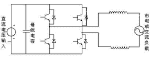
The combining inverter technology that the exists four pipe full-bridge circuit structures that adopt as shown in Figure 2, adopt bipolarity modulation system or unipolarity modulation system more at present.In the bipolarity modulation circuit, all with higher switching frequency work, the loss of switching tube is bigger, influences efficient for four switching tubes (shown in the frame of broken lines), and has bigger switching noise and current ripples amplitude.In the unipolarity modulation circuit, the common-mode voltage amplitude that inversion produces changes greatly, and consequent common mode current increases along with the increase of switching frequency is linear, and harmonic distortion and common-mode noise are disturbed more serious.
Summary of the invention
The objective of the invention is to overcome the deficiencies in the prior art, a kind of DC/AC grid-connected inverter circuit is provided, use three HF switch pipes to realize modulation, have two switching tubes to do the high frequency action at one time at most, effectively reduce the HF switch loss, improved conversion efficiency; When the output reactive power, only there is a HF switch plumber to do, can realize inversion simultaneously, be incorporated into the power networks and power factor controlling, it is the grid-connected inverter circuit with very strong overload capacity, wind-force, solar grid-connected inverter, microgrid inverter etc. and network source and inverter power supply technical applications can be widely used in, the requirement that power factor is regulated can be satisfied simultaneously.
The technical solution used in the present invention is: a kind of DC/AC grid-connected inverter circuit (as shown in Figure 1) comprises enhancement mode buck circuit, controllable silicon commutation circuit, inverter current sample circuit, voltage and current detection circuit, controllable silicon commutation control circuit and SPWM control circuit.When the required power factor was regulated: if the inverter active power of output, the enhancement mode buck circuit had only two each and every one power switchs to be in the SPWM modulation condition, and the another one power switch is in normally open; Regulate if inverter carries out reactive power, have only a power switch all to be on off state.
Described enhancement mode buck circuit comprises power switch Q1(MOSFET or IGBT), power switch Q2(MOSFET or IGBT), power switch Q3(MOSFET or IGBT) diode D1, diode D2, diode D3, inductance L 1, inductance L 2, capacitor C 1 and low frequency switch Q3, power switch Q1 drain electrode (or collector electrode) is joined with dc power anode and diode D2 negative electrode, and its source electrode (or emitter) joins with the negative electrode of inductance L 1 one ends, diode D1 negative electrode and diode D3; Power switch pipe Q2 drain electrode (or collector electrode) is connected with power switch pipe Q3 source electrode (or emitter) with an end of diode D2 anode, inductance L 2, and its source electrode (or emitter) joins with an end of anode, dc power cathode and the low frequency switch of diode D1; Power switch pipe Q2 drain electrode (or collector electrode) is connected with the drain electrode (or collector electrode) of power switch pipe Q2, the anode of diode D2 and an end of inductance L 2, and its source electrode (or emitter) is connected with diode D3; One end of inductance L 1 joins with the negative electrode of source electrode (or emitter), diode D1 negative electrode and the diode D3 of Q1, and the end of one-way SCR anode and C1 joins in the other end and the commutating circuit; One end of inductance L 2 is connected with the anode of D2 with Q2 drain electrode (or collector electrode) and is connected with the drain electrode (or collector electrode) of power switch pipe Q3, and the other end is connected with controllable silicon negative electrode, capacitor C 1.
Described controllable silicon commutation circuit comprises 4 unidirectional controllable silicon S 1 ~ S4, controllable silicon S1 forms the group of connecting with controllable silicon S2, controllable silicon S3 forms the group of connecting with controllable silicon S4, two series connection groups are in parallel, the anode of controllable silicon S1 and controllable silicon S3 joins, as the high voltage input, the negative electrode of controllable silicon S2 and controllable silicon S4 joins, as the low-voltage output.The tie point of the tie point of controllable silicon S1 and controllable silicon S2 and controllable silicon S3 and controllable silicon S4 connects to single-phase electrical network or AC load respectively as the single phase alternating current (A.C.) output.The driving signal of controllable silicon S1 and controllable silicon S4 is one group, and the driving signal of controllable silicon S2 and controllable silicon S3 is one group, and ON time respectively accounts for power frequency period half.
Described power switch Q1, power switch Q2 and power switch pipe Q3 are the HF switch pipe, and selecting device for use is MOSEFT or IGBT.
Described controllable silicon S1 ~ S4 is the low frequency switching tube, and selecting device for use is unidirectional controllable silicon S CR or IGBT.
Described power factor is regulated, when the inverter active power of output, an enhancement mode buck circuit power switch Q1 and power switch pipe Q2 are in the SPWM modulation condition, make another one power switch Q3 be in normally open, when Q1 and Q2 shutoff, constitute continuous current circuits with diode D3, inductance L 1 and inductance L 2.
Described power factor is regulated, and when inverter carries out the reactive power adjusting, has only power switch pipe Q3 to be in the SPWM modulation condition, Q1, Q2 are in normally off, when Q3 turn-offed simultaneously, D2, C2, D1, L1 and commutating circuit constituted continuous current circuit, realized the control of reactive power.
Enhancement mode buck circuit of the present invention is finished the half-sinusoid modulation and power factor is regulated.The control sequential that switching tube Q1, Q2 in the circuit, Q3 adopt is seen Fig. 4, and the direct current energy of dc bus C2 is converted to half-sinusoid; By adjusting the ON time of two groups of silicon controlled rectifiers, half-sinusoid is changed into sinusoidal all-wave; By adjusting the conduction mode of switching tube Q1, Q2, Q3, realize the power factor regulatory function.
Advantage of the present invention is:
Have only three HF switch pipes in the enhancement mode buck circuit in the entire circuit, and have only two high-frequency tube high frequency actions during active power output, have only a switching tube high frequency action during idle output, so the switching loss of switching tube is very little, inversion efficiency is greatly improved.
The pressure drop that inductance L 1 and inductance L 2 are born is half of traditional double polar mode, and the very big degree of current ripples and inductor loss reduces.
During reactive power output, has only a HF switch pipe action, idle delivery efficiency maximization.
Four power frequency controllable silicon overload capacity that adopt in the controllable silicon commutation circuit are strong, strengthen the stability of a system greatly, and devices switch loss and conduction loss are little, improved system effectiveness, device cost is low, can significantly reduce the cost of system, is conducive to popularizing of new forms of energy combining inverter;
Inverter circuit is symmetry fully, and the common-mode voltage that inversion produces is constant, produces common mode current thus and approaches zero, can effectively suppress common mode current, has reduced system's conduction loss, guarantees the quality of inverter current.
Basis at traditional Buck circuit in the enhancement mode buck circuit increases by two switching tubes, a diode and an inductance, can realize the power factor adjusting, can satisfy the adjustable demand of growing power factor.
The ingenious cooperation of enhancement mode buck circuit and commutation circuit has realized direct current input and the common mode inhibition that exchanges output, has effectively reduced EMI.
Description of drawings
Fig. 1 is that circuit of the present invention is formed schematic diagram.
Fig. 2 is conventional four pipe full bridge inverter schematic diagrams.
Fig. 3 is circuit theory diagrams of the present invention.
Fig. 4 is drives sequential chart of the present invention.
Fig. 5 is first quartile Q1 of the present invention, Q2 conducting isoboles
Fig. 6 is that first quartile Q1 of the present invention, Q2 turn-off isoboles.
Fig. 7 is the present invention's second quadrant Q3 conducting isoboles.
Fig. 8 is that the present invention second quadrant Q3 turn-offs isoboles.
Fig. 9 is third quadrant Q1 of the present invention, Q2 conducting isoboles.
Figure 10 is that third quadrant Q1 of the present invention, Q2 turn-off isoboles.
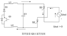
Figure 11 is fourth quadrant Q3 conducting isoboles of the present invention.
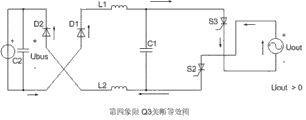
Figure 12 is that fourth quadrant Q3 of the present invention turn-offs isoboles.
Embodiment
As Fig. 1, Fig. 3, shown in Figure 4, the DC/AC grid-connected inverter circuit comprises enhancement mode buck circuit, controllable silicon commutation circuit, inverter current sample circuit, voltage and current detection circuit, controllable silicon commutation control circuit and SPWM control circuit.
Described enhancement mode buck circuit comprises power switch Q1(MOSFET or IGBT), power switch Q2(MOSFET or IGBT), power switch Q3(MOSFET or IGBT) diode D1, diode D2, diode D3, inductance L 1, inductance L 2, capacitor C 1 and low frequency switch Q3, power switch Q1 drain electrode (or collector electrode) is joined with dc power anode and diode D2 negative electrode, and its source electrode (or emitter) joins with the negative electrode of inductance L 1 one ends, diode D1 negative electrode and diode D3; Power switch pipe Q2 drain electrode (or collector electrode) is connected with power switch pipe Q3 source electrode (or emitter) with an end of diode D2 anode, inductance L 2, and its source electrode (or emitter) joins with an end of anode, dc power cathode and the low frequency switch of diode D1; Power switch pipe Q2 drain electrode (or collector electrode) is connected with the drain electrode (or collector electrode) of power switch pipe Q2, the anode of diode D2 and an end of inductance L 2, and its source electrode (or emitter) is connected with diode D3; One end of inductance L 1 joins with the negative electrode of source electrode (or emitter), diode D1 negative electrode and the diode D3 of Q1, and the end of one-way SCR anode and C1 joins in the other end and the commutating circuit; One end of inductance L 2 is connected with the anode of D2 with Q2 drain electrode (or collector electrode) and is connected with the drain electrode (or collector electrode) of power switch pipe Q3, and the other end is connected with controllable silicon negative electrode, capacitor C 1.
Described controllable silicon commutation circuit comprises 4 unidirectional controllable silicon S 1 ~ S4, controllable silicon S1 forms the group of connecting with controllable silicon S2, controllable silicon S3 forms the group of connecting with controllable silicon S4, two series connection groups are in parallel, the anode of controllable silicon S1 and controllable silicon S3 joins, as the high voltage input, the negative electrode of controllable silicon S2 and controllable silicon S4 joins, as the low-voltage output.The tie point of the tie point of controllable silicon S1 and controllable silicon S2 and controllable silicon S3 and controllable silicon S4 connects to single-phase electrical network or AC load respectively as the single phase alternating current (A.C.) output.The driving signal of controllable silicon S1 and controllable silicon S4 is one group, and the driving signal of controllable silicon S2 and controllable silicon S3 is one group, and ON time respectively accounts for power frequency period half.
As shown in Figure 4, press voltage and sense of current, each power frequency period can be divided into 4 stages: first quartile, output voltage are greater than zero, and output current is greater than zero; Second quadrant, output voltage are less than zero, and output current is greater than zero; Third quadrant, output voltage are less than zero, and output current is less than zero; Fourth quadrant, output voltage are greater than zero, and output current is less than zero.Provided the driving signal of power switch pipe Q1, Q2, Q3 and controllable silicon S1 ~ S4 in each quadrant among Fig. 4.Below in conjunction with legend each stage is described further.
1. first quartile, output voltage are greater than zero, and output current is greater than zero.
Output current is greater than zero, S1, S4 conducting, and switching tube Q3 often opens, and switching tube Q1, Q2 are driven signal generation pattern and are seen Fig. 4 by the control of SPWM output signal.
When Q1, Q2 conducting, isoboles is seen Fig. 5, and DC source is outwards transmitted energy by inductance L 1, the conduction voltage drop of ignoring device, inductance both end voltage UL=Ubus – Uout is greater than zero, so inductive current increases gradually, inductive energy storage increases gradually, and current circuit is shown in arrow among the figure.
When Q1, Q2 turn-offed, isoboles was seen Fig. 6, and inductance continues outwards to transmit energy.The conduction voltage drop of ignoring device, inductance both end voltage UL=– Uout is less than zero, so inductive current progressively reduces, the energy of storage progressively reduces, current circuit is shown in arrow among the figure.
2. second quadrant, output voltage are less than zero, and output current is greater than zero.
Output current is greater than zero, S1, S4 conducting, and switching tube Q1 and Q2 are normally closed, and just SPWM modulation of switching tube Q3 drives signal generation pattern and sees Fig. 4.
When Q3 conducting simultaneously, isoboles is seen Fig. 7, and inductance continues outwards to transmit energy.The conduction voltage drop of ignoring device, inductance both end voltage UL=-Uout is greater than zero, so inductive current progressively increases, the energy of storage progressively reduces, and current circuit is shown in arrow among the figure.
When Q3 turn-offed simultaneously, isoboles was seen Fig. 8, and inductance continues outwards to transmit energy.The conduction voltage drop of ignoring device, inductance both end voltage UL=-Ubus-Uout is less than zero, so inductive current progressively reduces, the energy of storage progressively reduces, and current circuit is shown in arrow among the figure.
3. third quadrant, output voltage are less than zero, and output current is less than zero.
Output current is less than zero, S2, S3 conducting, and Q3 is in conducting state all the time, and switching tube Q1 and switching tube Q2 are driven signal generation pattern and are seen Fig. 4 by the control of SPWM output signal.
When Q1, Q2 conducting simultaneously, isoboles is seen Fig. 9, and DC source is outwards transmitted energy by inductance L 1.The conduction voltage drop of ignoring device, inductance both end voltage UL=Ubus+Uout is greater than zero, so inductive current increases gradually, inductive energy storage increases gradually, current circuit is shown in arrow among the figure.
When Q1, Q2 turn-offed simultaneously, isoboles was seen Figure 10, and inductance continues outwards to transmit energy.The conduction voltage drop of ignoring device, inductance both end voltage UL=Uout is less than zero, so inductive current progressively reduces, the energy of storage progressively reduces, current circuit is shown in arrow among the figure.
4. fourth quadrant, output voltage are greater than zero, and output current is less than zero, and switching tube Q1 and Q2 are normally closed, and switching tube Q3 carries out the SPWM modulation, drive signal generation pattern and see Fig. 4.
When Q1, Q2 conducting simultaneously, isoboles is seen Figure 11, and DC source is outwards transmitted energy by inductance L 1.The conduction voltage drop of ignoring device, inductance both end voltage UL=Uout is greater than zero, so inductive current increases gradually, inductive energy storage increases gradually, current circuit is shown in arrow among the figure.
When Q3 turn-offed, isoboles was seen Figure 12, and inductance continues outwards to transmit energy.The conduction voltage drop of ignoring device, inductance both end voltage UL=-Ubus+Uout is less than zero, so inductive current progressively reduces, the energy of storage progressively reduces, and current circuit is shown in arrow among the figure.
Claims (7)
1. a grid-connected inverter circuit is characterized in that comprising enhancement mode buck circuit, controllable silicon commutation circuit, inverter current sample circuit, voltage and current detection circuit, controlled rectifier commutation control circuit and SPWM control circuit.
2. enhancement mode buck circuit according to claim 1, it is characterized in that: comprise power switch Q1(MOSFET or IGBT), power switch Q2(MOSFET or IGBT), power switch Q3(MOSFET or IGBT) diode D1, diode D2, diode D3, inductance L 1, inductance L 2, capacitor C 1 and low frequency switch Q3, power switch Q1 drain electrode (or collector electrode) is joined with dc power anode and diode D2 negative electrode, and its source electrode (or emitter) joins with the negative electrode of inductance L 1 one ends, diode D1 negative electrode and diode D3; Power switch pipe Q2 drain electrode (or collector electrode) is connected with power switch pipe Q3 source electrode (or emitter) with an end of diode D2 anode, inductance L 2, and its source electrode (or emitter) joins with an end of anode, dc power cathode and the low frequency switch of diode D1; Power switch pipe Q2 drain electrode (or collector electrode) is connected with the drain electrode (or collector electrode) of power switch pipe Q2, the anode of diode D2 and an end of inductance L 2, and its source electrode (or emitter) is connected with diode D3; One end of inductance L 1 joins with the negative electrode of source electrode (or emitter), diode D1 negative electrode and the diode D3 of Q1, and the end of one-way SCR anode and C1 joins in the other end and the commutating circuit; One end of inductance L 2 is connected with the anode of D2 with Q2 drain electrode (or collector electrode) and is connected with the drain electrode (or collector electrode) of power switch pipe Q3, and the other end is connected with controllable silicon negative electrode, capacitor C 1.
3. grid-connected inverter circuit according to claim 1, it is characterized in that: described controllable silicon commutation circuit comprises 4 unidirectional controllable silicon S 1 ~ S4, controllable silicon S1 forms the group of connecting with controllable silicon S2, controllable silicon S3 forms the group of connecting with controllable silicon S4, two series connection groups are in parallel, and the anode of controllable silicon S1 and controllable silicon S3 joins, as the high voltage input, the negative electrode of controllable silicon S2 and controllable silicon S4 joins, as the low-voltage output; The tie point of the tie point of controllable silicon S1 and controllable silicon S2 and controllable silicon S3 and controllable silicon S4 connects to single-phase electrical network or AC load respectively as the single phase alternating current (A.C.) output; The driving signal of controllable silicon S1 and controllable silicon S4 is one group, and the driving signal of controllable silicon S2 and controllable silicon S3 is one group, and ON time respectively accounts for power frequency period half; Break-make by control Q3 realizes power factor controlling.
4. grid-connected inverter circuit according to claim 2, it is characterized in that: described power switch Q1, power switch Q2 and power switch pipe Q3 are the HF switch pipe, selecting device for use is MOSEFT or IGBT.
5. grid-connected inverter circuit according to claim 3, it is characterized in that: described controllable silicon S1 ~ S4 is the low frequency switching tube, selecting device for use is unidirectional controllable silicon S CR or IGBT.
6. described power factor controlling according to claim 3, it is characterized in that: when the inverter active power of output, an enhancement mode buck circuit power switch Q1 and power switch pipe Q2 are in the SPWM modulation condition, make another one power switch Q3 be in normally open, when Q1 and Q2 shutoff, constitute continuous current circuits with diode D3, inductance L 1 and inductance L 2.
7. described power factor controlling according to claim 3, it is characterized in that: when inverter carries out the reactive power adjusting, have only power switch pipe Q3 to be in the SPWM modulation condition, Q1, Q2 are in normally off, when Q3 turn-offs simultaneously, D2, C2, D1, L1 and commutating circuit constitute continuous current circuit, realize the control of reactive power.
Priority Applications (1)
| Application Number | Priority Date | Filing Date | Title |
|---|---|---|---|
| CN2012100105856A CN103208935A (en) | 2012-01-14 | 2012-01-14 | Low-common-mode-noise grid-connected inverter circuit and reactive power control method |
Applications Claiming Priority (1)
| Application Number | Priority Date | Filing Date | Title |
|---|---|---|---|
| CN2012100105856A CN103208935A (en) | 2012-01-14 | 2012-01-14 | Low-common-mode-noise grid-connected inverter circuit and reactive power control method |
Publications (1)
| Publication Number | Publication Date |
|---|---|
| CN103208935A true CN103208935A (en) | 2013-07-17 |
Family
ID=48756046
Family Applications (1)
| Application Number | Title | Priority Date | Filing Date |
|---|---|---|---|
| CN2012100105856A Pending CN103208935A (en) | 2012-01-14 | 2012-01-14 | Low-common-mode-noise grid-connected inverter circuit and reactive power control method |
Country Status (1)
| Country | Link |
|---|---|
| CN (1) | CN103208935A (en) |
Cited By (6)
| Publication number | Priority date | Publication date | Assignee | Title |
|---|---|---|---|---|
| DE102014102000B3 (en) * | 2014-02-18 | 2014-09-11 | Sma Solar Technology Ag | Method for operating a power inverter with blind inverters with pole turner and reactive power inverter with polarity reverser |
| DE102015113071A1 (en) * | 2015-08-07 | 2017-02-09 | Sma Solar Technology Ag | Potential-shifting half-bridge, pole-reverser and reactive power inverters as well as Polwendeverfahren |
| CN107302319A (en) * | 2017-06-14 | 2017-10-27 | 珠海格力电器股份有限公司 | Single-phase sinewave inverter and its control method |
| CN108351661A (en) * | 2015-12-04 | 2018-07-31 | 东芝三菱电机产业系统株式会社 | Power conversion system |
| US10530273B2 (en) | 2015-08-07 | 2020-01-07 | Sma Solar Technology Ag | Unfolding bridge, inverter having reactive-power capability, and polarity reversing method |
| CN113162380A (en) * | 2021-03-30 | 2021-07-23 | 闽南理工学院 | System and method for improving EMC performance of inverter-driven power supply |
Citations (6)
| Publication number | Priority date | Publication date | Assignee | Title |
|---|---|---|---|---|
| JPH02266870A (en) * | 1989-04-05 | 1990-10-31 | Mitsubishi Electric Corp | Power conversion device for battery |
| CN101552569A (en) * | 2008-12-10 | 2009-10-07 | 南京航空航天大学 | Synchronization inverter main circuit topology |
| CN101582592A (en) * | 2008-05-15 | 2009-11-18 | 宣昆 | Transless photovoltaic merging and inverting device and control method thereof |
| CN102088193A (en) * | 2011-03-04 | 2011-06-08 | 东南大学 | Photovoltaic synchronization grid full bridge six-switching tube inverter and control method thereof |
| CN102255544A (en) * | 2011-07-25 | 2011-11-23 | 无锡风光新能源科技有限公司 | DC (direct current)/AC (alternating current) inverter circuit |
| CN102403922A (en) * | 2011-12-21 | 2012-04-04 | 牟英峰 | DC/AC grid connected inverter circuit and power factor adjusting method |
-
2012
- 2012-01-14 CN CN2012100105856A patent/CN103208935A/en active Pending
Patent Citations (6)
| Publication number | Priority date | Publication date | Assignee | Title |
|---|---|---|---|---|
| JPH02266870A (en) * | 1989-04-05 | 1990-10-31 | Mitsubishi Electric Corp | Power conversion device for battery |
| CN101582592A (en) * | 2008-05-15 | 2009-11-18 | 宣昆 | Transless photovoltaic merging and inverting device and control method thereof |
| CN101552569A (en) * | 2008-12-10 | 2009-10-07 | 南京航空航天大学 | Synchronization inverter main circuit topology |
| CN102088193A (en) * | 2011-03-04 | 2011-06-08 | 东南大学 | Photovoltaic synchronization grid full bridge six-switching tube inverter and control method thereof |
| CN102255544A (en) * | 2011-07-25 | 2011-11-23 | 无锡风光新能源科技有限公司 | DC (direct current)/AC (alternating current) inverter circuit |
| CN102403922A (en) * | 2011-12-21 | 2012-04-04 | 牟英峰 | DC/AC grid connected inverter circuit and power factor adjusting method |
Cited By (8)
| Publication number | Priority date | Publication date | Assignee | Title |
|---|---|---|---|---|
| DE102014102000B3 (en) * | 2014-02-18 | 2014-09-11 | Sma Solar Technology Ag | Method for operating a power inverter with blind inverters with pole turner and reactive power inverter with polarity reverser |
| DE102015113071A1 (en) * | 2015-08-07 | 2017-02-09 | Sma Solar Technology Ag | Potential-shifting half-bridge, pole-reverser and reactive power inverters as well as Polwendeverfahren |
| DE102015113071B4 (en) | 2015-08-07 | 2018-06-07 | Sma Solar Technology Ag | Potential-shifting half-bridge, pole-reverser and reactive power inverters as well as Polwendeverfahren |
| US10530273B2 (en) | 2015-08-07 | 2020-01-07 | Sma Solar Technology Ag | Unfolding bridge, inverter having reactive-power capability, and polarity reversing method |
| EP3332466B1 (en) * | 2015-08-07 | 2020-11-11 | SMA Solar Technology AG | Polarity reverser, inverter having reactive-power capability, and polarity reversing method |
| CN108351661A (en) * | 2015-12-04 | 2018-07-31 | 东芝三菱电机产业系统株式会社 | Power conversion system |
| CN107302319A (en) * | 2017-06-14 | 2017-10-27 | 珠海格力电器股份有限公司 | Single-phase sinewave inverter and its control method |
| CN113162380A (en) * | 2021-03-30 | 2021-07-23 | 闽南理工学院 | System and method for improving EMC performance of inverter-driven power supply |
Similar Documents
| Publication | Publication Date | Title |
|---|---|---|
| CN102185514B (en) | Single-phase three-level inverter | |
| CN103051233B (en) | Non-isolated single-phase photovoltaic grid-connected inverter and on-off control timing sequence thereof | |
| CN103199727B (en) | Zero current switching full-bridge type non-isolated photovoltaic grid-connected inverter | |
| WO2012163235A1 (en) | Inverter topology circuit, inversion method and inveter | |
| CN102005954B (en) | Single-phase non-isolated photovoltaic grid-connected inverter and control method | |
| CN101951186A (en) | Soft switching three-phase gird-connected inverter additionally provided with freewheeling path | |
| CN102856916A (en) | Reactive power control method and circuit of single-phase photovoltaic inverter | |
| CN103326606B (en) | A kind of one-phase five-level inverter | |
| CN103208935A (en) | Low-common-mode-noise grid-connected inverter circuit and reactive power control method | |
| CN102255544A (en) | DC (direct current)/AC (alternating current) inverter circuit | |
| CN112928919B (en) | Isolated high-frequency resonant DC-DC converter with wide output voltage range and method | |
| CN202524315U (en) | DC/AC grid-connected inversion circuit | |
| CN104242719A (en) | Switching-loss-free full-bridge non-isolated photovoltaic grid-connected inverter and on-off control timing sequence | |
| CN110086360A (en) | A kind of five level high efficiency rectifiers | |
| CN104410310A (en) | Neutral point clamped H-bridge photovoltaic inverter and method for inhibiting common mode leakage current | |
| CN102403922A (en) | DC/AC grid connected inverter circuit and power factor adjusting method | |
| CN102684530A (en) | Method for controlling transformerless inverter with reactive power compensation function | |
| CN201994871U (en) | Photovoltaic grid six-switch tube bridge inverter | |
| CN109713929B (en) | Three-phase three-switch two-level rectifier based on zero-voltage soft switch | |
| CN101783608A (en) | Minimum-voltage, active-clamp and three-phase grid-connected inverter | |
| CN105186914A (en) | Novel H6 single-phase non-isolation grid-connected inverter | |
| CN205029572U (en) | Novel single -phase non - isolation grid -connected inverter of H6 | |
| CN102347697B (en) | Direct DC-AC (direct current-alternating current) converting circuit for low-voltage input full bridge inverter | |
| CN103269174B (en) | A kind of single-phase photovoltaic grid-connected inverter of low common-mode voltage | |
| CN102769394B (en) | Single-phase controllable rectification circuit |
Legal Events
| Date | Code | Title | Description |
|---|---|---|---|
| C06 | Publication | ||
| PB01 | Publication | ||
| C10 | Entry into substantive examination | ||
| SE01 | Entry into force of request for substantive examination | ||
| C02 | Deemed withdrawal of patent application after publication (patent law 2001) | ||
| WD01 | Invention patent application deemed withdrawn after publication |
Application publication date: 20130717 |