WO2023182303A1 - Motor drive device - Google Patents
Motor drive device Download PDFInfo
- Publication number
- WO2023182303A1 WO2023182303A1 PCT/JP2023/010992 JP2023010992W WO2023182303A1 WO 2023182303 A1 WO2023182303 A1 WO 2023182303A1 JP 2023010992 W JP2023010992 W JP 2023010992W WO 2023182303 A1 WO2023182303 A1 WO 2023182303A1
- Authority
- WO
- WIPO (PCT)
- Prior art keywords
- signal
- circuit
- current
- pulse
- switch element
- Prior art date
Links
- 238000001514 detection method Methods 0.000 claims abstract description 59
- 238000010586 diagram Methods 0.000 description 34
- 230000007423 decrease Effects 0.000 description 11
- 230000003111 delayed effect Effects 0.000 description 8
- 230000002238 attenuated effect Effects 0.000 description 6
- 238000000034 method Methods 0.000 description 3
- 230000001172 regenerating effect Effects 0.000 description 3
- 230000003247 decreasing effect Effects 0.000 description 2
- 230000000694 effects Effects 0.000 description 2
- 230000004048 modification Effects 0.000 description 2
- 238000012986 modification Methods 0.000 description 2
- 230000008569 process Effects 0.000 description 2
- 239000000470 constituent Substances 0.000 description 1
- 239000000463 material Substances 0.000 description 1
- 230000004044 response Effects 0.000 description 1
- 239000007787 solid Substances 0.000 description 1
- 230000007704 transition Effects 0.000 description 1
Images


Classifications
-
- H—ELECTRICITY
- H02—GENERATION; CONVERSION OR DISTRIBUTION OF ELECTRIC POWER
- H02P—CONTROL OR REGULATION OF ELECTRIC MOTORS, ELECTRIC GENERATORS OR DYNAMO-ELECTRIC CONVERTERS; CONTROLLING TRANSFORMERS, REACTORS OR CHOKE COILS
- H02P27/00—Arrangements or methods for the control of AC motors characterised by the kind of supply voltage
- H02P27/04—Arrangements or methods for the control of AC motors characterised by the kind of supply voltage using variable-frequency supply voltage, e.g. inverter or converter supply voltage
- H02P27/06—Arrangements or methods for the control of AC motors characterised by the kind of supply voltage using variable-frequency supply voltage, e.g. inverter or converter supply voltage using dc to ac converters or inverters
- H02P27/08—Arrangements or methods for the control of AC motors characterised by the kind of supply voltage using variable-frequency supply voltage, e.g. inverter or converter supply voltage using dc to ac converters or inverters with pulse width modulation
Definitions
- the present disclosure relates to a motor drive device.
- Motor drive devices that drive a motor with low noise and low vibration include one disclosed in Patent Document 1, for example.
- the motor drive device disclosed in Patent Document 1 uses a resistor to detect the current flowing through the motor coil due to the switching operation of a switch element, and applies PWM (Pulse Width Modulation) to the current so that the peak value of the detected voltage follows a reference voltage.
- PWM Pulse Width Modulation
- the aim is to achieve low noise and vibration through pulse width modulation (pulse width modulation) control.
- the reference voltage is a voltage that sets a target value of the current flowing through the motor coil.
- Patent Document 1 also discloses a countermeasure by switching the switching operation mode near the zero-crossing point.
- the setting of the minimum on-period differs depending on the characteristics of the switch element, and the minimum on-period is set to be long with some margin due to the versatility of the switch element drive circuit, so the current waveform deviates from the target waveform near the zero-crossing point. The problem becomes obvious.
- the present disclosure solves these problems and provides a motor drive device that can cause a current waveform near a zero-crossing point to accurately follow a target waveform.
- a motor drive device that drives a motor, and includes a first series switch circuit including a first high side switch element and a first low side switch element, and a first series switch circuit including a first high side switch element and a first low side switch element.
- a second series switch circuit including a second high-side switch element and a second low-side switch element and connected in parallel to the first series switch circuit, and a reference pulse signal having a pulse duration greater than zero; a reference pulse generation circuit that generates a reference pulse with a period of , a current detection unit that outputs a current signal corresponding to a motor current that is a current flowing through the motor, and a reference that generates a reference waveform signal that corresponds to a control target value of the motor current.
- a waveform generation circuit a current comparison circuit that compares the current signal and the reference waveform signal to generate a comparison signal; the reference pulse signal, the reference waveform signal, and the comparison signal are input; a PWM circuit that outputs a signal and a second drive signal, and a first connection point that is a connection point between the first high-side switch element and the first low-side switch element; The motor is connected between a second connection point that is a connection point between the second high-side switch element and the second low-side switch element, and the first drive signal is connected to the start of the reference pulse signal.
- the second drive signal includes a first pulse that is terminated, and the second drive signal is configured to terminate the first pulse if the absolute value of the current signal exceeds the absolute value of the reference waveform signal within the pulse duration.
- the PWM circuit includes a second pulse that is started after the end of the pulse and is continued for at least a period until the absolute value of the current signal becomes lower than the absolute value of the reference waveform signal, and the PWM circuit includes: During a first period in which the motor current mainly flows from the first connection point to the second connection point, the first drive signal is output to the first series switch circuit, and the second drive signal is output to the first series switch circuit. is output to the second series switch circuit, and during a second period in which the motor current mainly flows from the second connection point to the first connection point, the second drive signal is output to the first series switch circuit. and outputs the first drive signal to the second series switch circuit.
- a motor drive device that can cause a current waveform near a zero-crossing point to accurately follow a target waveform.
- FIG. 1A is a circuit configuration diagram of a motor drive device according to Embodiment 1.
- FIG. 1B is a graph showing an example of the waveforms of the polarity instruction signal, the first reference waveform signal, and the second reference waveform signal according to the first embodiment.
- FIG. 2 is a graph showing an example of the waveform of each signal in sections A1 and A2 of FIG. 1B.
- FIG. 3A is a state diagram showing the state of each switch element and the current path in section A1 of FIG. 1B.
- FIG. 3B is a state diagram showing the state of each switch element and the current path in section A2 of FIG. 1B.
- FIG. 4 is a graph showing an example of the waveform of each signal in section B of FIG. 1B.
- FIG. 5 is a state diagram showing the state of each switch element and the path of flowing current in section B of FIG. 1B.
- FIG. 6 is a graph showing an example of the waveform of each signal in section C of FIG. 1B.
- FIG. 7A is a circuit configuration diagram of a motor drive device according to Embodiment 2.
- FIG. 7B is a graph showing an example of the waveforms of the polarity instruction signal and the reference waveform signal according to the second embodiment.
- FIG. 8 is a graph showing an example of the waveform of each signal in sections A1 and A2 of FIG. 7B.
- FIG. 9 is a graph showing an example of the waveform of each signal in section B of FIG. 7B.
- FIG. 10 is a graph showing an example of the waveform of each signal in section C of FIG. 7B.
- each figure is a schematic diagram and is not necessarily strictly illustrated. Therefore, the scale etc. in each figure are not necessarily the same.
- symbol is attached to the substantially the same structure, and the overlapping description is omitted or simplified.
- FIG. 1A is a circuit configuration diagram of a motor drive device 10 according to the present embodiment.
- FIG. 1A also shows a motor 3 driven by the motor drive device 10 and an input power source 1 that supplies DC power to the motor drive device 10.
- the input power supply 1 supplies a power supply voltage Vcc between a power supply line and a ground line.
- the input power source 1 is, for example, a battery.
- the motor drive device 10 is a device that drives the motor 3.
- the motor drive device 10 includes a first series switch circuit 31, a second series switch circuit 32, a reference pulse generation circuit 50, a current detection resistor 4, a PWM circuit 5, a reference waveform generation circuit 51, and a current It has a comparison circuit 8.
- the first series switch circuit 31 is a series circuit including a first high-side switch element 21 and a first low-side switch element 23.
- the first high-side switch element 21 and the first low-side switch element 23 are connected in series at a first connection point X1.
- the first connection point X1 is a connection point between the first high-side switch element 21 and the first low-side switch element 23.
- the first series switch circuit 31 further includes an inverter 25.
- the inverter 25 is connected between the control terminal of the first low-side switch element 23 and the control terminal of the first high-side switch element 21, and is input to the control terminal of the first high-side switch element 21.
- a drive signal V3, which is an inverted signal of the drive signal V1, is input to the control terminal of the first low-side switch element 23.
- the second series switch circuit 32 is a series circuit that includes a second high-side switch element 22 and a second low-side switch element 24 and is connected in parallel to the first series switch circuit 31.
- the second high-side switch element 22 and the second low-side switch element 24 are connected in series at a second connection point X2.
- the second connection point X2 is a connection point between the second high-side switch element 22 and the second low-side switch element 24.
- the first high-side switch element 21 and the second high-side switch element 22 are connected by a power supply line, and the first low-side switch element 23 and the second low-side switch element 24 are connected.
- the second series switch circuit 32 further includes an inverter 26.
- the inverter 26 is connected between the control terminal of the second low-side switch element 24 and the control terminal of the second high-side switch element 22, and is input to the control terminal of the second high-side switch element 22.
- a drive signal V4 which is an inverted signal of the drive signal V2, is input to the control terminal of the second low-side switch element 24.
- the configurations of the first high-side switch element 21, the second high-side switch element 22, the first low-side switch element 23, and the second low-side switch element 24 are not particularly limited.
- an N-channel MOSFET can be used as each switch element.
- a P-channel MOSFET as each switch element by inverting the signal input to the control terminal of each switch element.
- each of the ideal switches has a body diode, and when a high level (that is, H level) drive signal is applied to the control terminal, conduction occurs between the first terminal and the second terminal and turns on. The switch element will be explained.
- the motor 3 is connected between a first connection point X1 and a second connection point X2 of a bridge circuit including a first series switch circuit 31 and a second series switch circuit 32.
- the current detection resistor 4 is an example of a current detection unit that outputs a current signal corresponding to the motor current IL, which is the current flowing through the motor 3.
- the current detection resistor 4 is a resistance element connected between the connection point of the first low-side switch element 23 and the second low-side switch element 24 and the ground line. Below, the resistance value of the current detection resistor 4 will be expressed as Rs.
- the bridge circuit including the first series switch circuit 31 and the second series switch circuit 32, the motor 3, and the current detection resistor 4 are connected between the power supply line and the ground line. Ru.
- each high-side switch element and each low-side switch element are turned on and off alternately, but in reality, each high-side switch element and each low-side switch element are turned on and off alternately.
- a period called a dead time is provided, which is a period during which both the switch element and each low-side switch element are in an off state.
- there is also an operation mode that provides a period in which each high-side switch element and each low-side switch element are both in an OFF state.
- Such operation is a well-known technique and is not the gist of the present disclosure. Therefore, in the present disclosure, in order to avoid complicating the explanation, illustrations and explanations of such operations are omitted, and each high-side switch element and each low-side switch element are turned on and off simultaneously and alternately. It will be explained as follows.
- the reference pulse generation circuit 50 is a circuit that generates a reference pulse signal P0 having a pulse duration (that is, pulse width) greater than zero at a predetermined period. This pulse duration is also referred to as the minimum on-period.
- the pulse duration and the predetermined period are not particularly limited. In this embodiment, the pulse duration is 2 microseconds and the predetermined period is 10 microseconds.
- the reference waveform generation circuit 51 is a circuit that generates a reference waveform signal corresponding to the control target value of the motor current IL.
- the reference waveform signal includes a first reference waveform signal and a second reference waveform signal.
- a first reference waveform signal serving as a control target waveform of a motor current IL flowing in a direction (hereinafter also referred to as forward direction) from the first connection point X1 to the second connection point X2 according to the rotational position of the motor 3.
- Vr1 the second reference waveform signal Vr2 which is the control target waveform of the motor current flowing in the direction (hereinafter also referred to as negative direction) from the second connection point X2 to the first connection point X1, and the motor current IL.
- Polarity instruction signal DIR is a signal that controls the direction of motor current IL.
- the polarity instruction signal DIR is output to the PWM circuit 5.
- the motor current IL is positive when the polarity instruction signal DIR is at a high level, and is negative when the polarity instruction signal DIR is at a low level (that is, an L level). That is, the period during which the polarity instruction signal DIR is at a high level mainly corresponds to the first period in which the motor current IL flows from the first connection point X1 to the second connection point X2.
- the period during which the polarity instruction signal DIR is at a low level mainly corresponds to a second period during which the motor current IL flows from the second connection point X2 to the first connection point X1.
- FIG. 1B is a graph showing an example of the waveforms of the polarity instruction signal DIR, the first reference waveform signal Vr1, and the second reference waveform signal Vr2 according to the present embodiment.
- Graph (a) in FIG. 1B is a graph showing the waveform of the polarity instruction signal DIR.
- Graph (b) in FIG. 1B is a graph showing the waveforms of the first reference waveform signal Vr1 and the second reference waveform signal Vr2.
- the horizontal axis of each graph represents time.
- the solid curve shows the waveform of the first reference waveform signal Vr1
- the broken line curve shows the waveform of the second reference waveform signal Vr2.
- the first reference waveform signal Vr1 is a signal that periodically oscillates in positive and negative directions with a reference amplitude.
- the second reference waveform signal Vr2 is a signal that periodically oscillates in positive and negative directions with a reference amplitude and in an opposite phase to the first reference waveform signal Vr1. That is, the second reference waveform signal Vr2 is a signal obtained by inverting the sign of the first reference waveform signal Vr1.
- each reference waveform signal is a trapezoidal wave, but it may have a waveform such as a sine wave.
- the switching period of each switch element is sufficiently shorter than the period of each reference waveform signal, and in the following description, it is assumed that each reference waveform signal has a constant value during several periods of the switching operation.
- the current comparison circuit 8 is a circuit that compares the current signal and the reference waveform signal to generate a comparison signal.
- the comparison signal includes a first comparison signal C1 and a second comparison signal C2, and the current comparison circuit 8 compares the current signal and the first reference waveform signal Vr1 to obtain a first comparison signal C1 and a second comparison signal C2.
- a first comparison circuit 55 that generates the first comparison signal C1; and a second comparison circuit 56 that compares the current signal and the second reference waveform signal Vr2 to generate the second comparison signal C2.
- a current detection voltage Vs of the current detection resistor 4 is inputted to each comparison circuit as a current signal.
- the first comparison signal C1 is inverted when the motor current IL is the first target waveform value Vr1/Rs, and the second comparison signal C2 is inverted.
- the inversion occurs when the motor current IL reaches the second target waveform value Vr2/Rs.
- a differential amplifier circuit or the like can be used as the first comparison circuit 55 and the second comparison circuit 56.
- the PWM circuit 5 is a circuit into which a reference pulse signal, a reference waveform signal, and a comparison signal are input, and outputs a first drive signal and a second drive signal.
- the PWM circuit 5 outputs a first drive signal to the first series switch circuit 31 and outputs a first drive signal to the first series switch circuit 31 mainly during a first period in which the motor current IL flows from the first connection point X1 to the second connection point X2.
- the drive signal is output to the second series switch circuit 32.
- the PWM circuit 5 outputs the second drive signal to the first series switch circuit 31 mainly during the second period in which the motor current IL flows from the second connection point X2 to the first connection point X1,
- the first drive signal is output to the second series switch circuit 32.
- the first drive signal is a first pulse that is started in synchronization with the start of the reference pulse signal, and the absolute value of the current signal is a reference waveform after a pulse duration has elapsed from the beginning of the reference pulse signal. It includes a first pulse that is terminated when the absolute value of the signal is exceeded.
- the first pulse is raised in accordance with the rise of the reference pulse signal, and the first pulse is started after the pulse duration of the reference pulse signal has elapsed and the absolute value of the current signal is equal to that of the reference waveform signal. It includes a first pulse that falls when the absolute value is exceeded.
- the second drive signal is a second pulse that is started after the end of the first pulse when the absolute value of the current signal exceeds the absolute value of the reference waveform signal within the pulse duration of the reference pulse signal.
- the second pulse is maintained at least until the absolute value of the current signal becomes lower than the absolute value of the reference waveform signal.
- the second drive signal does not include a pulse if the absolute value of the current signal does not exceed the absolute value of the reference waveform signal within the pulse duration of the reference pulse signal.
- the second drive signal is maintained at a low level if the absolute value of the current signal does not exceed the absolute value of the reference waveform signal within the pulse duration of the reference pulse signal.
- the second pulse when the absolute value of the current signal exceeds the absolute value of the reference waveform signal within the pulse duration time of the reference pulse signal, the second pulse is raised after the first pulse ends.
- the PWM circuit 5 includes a first pulse output circuit 52, a second pulse output circuit 53, a first PWM circuit 6, and a second PWM circuit 7.
- the first pulse output circuit 52 receives a reference pulse signal P0, and a first pulse output circuit 52 includes a first pulse that is output during a first period in which the motor current IL mainly flows from the first connection point X1 to the second connection point X2. This is a circuit that outputs a reference pulse signal P1.
- the first pulse output circuit 52 receives the reference pulse signal P0 and the polarity instruction signal DIR, and outputs the first reference pulse signal P1.
- an AND circuit can be used as the first pulse output circuit 52.
- the second pulse output circuit 53 receives the reference pulse signal P0 and outputs a second pulse including pulses mainly output during a second period in which the motor current IL flows from the second connection point X2 to the first connection point X1.
- This circuit outputs the reference pulse signal P2.
- the second pulse output circuit 53 receives the reference pulse signal P0 and the inverted signal of the polarity instruction signal DIR, and outputs the second reference pulse signal P2.
- an AND circuit can be used as the second pulse output circuit 53.
- the inverted signal of the polarity instruction signal DIR is obtained by inputting the polarity instruction signal DIR to the inverter 54.
- the first PWM circuit 6 mainly operates from the first connection point X1 to the During the first period in which the motor current IL flows to the connection point X2 of the second connection point X2, the first drive signal is output to the first series switch circuit 31, and the first drive signal is mainly passed from the second connection point X2 to the first connection point X1.
- This circuit outputs the second drive signal during the second period when the motor current IL flows.
- the signal output by the first PWM circuit 6 corresponds to the drive signal V1 input to the control terminal of the first high-side switch element 21.
- the first PWM circuit 6 includes OR circuits 60, 62, 66, D flip-flops 61, 63, inverters 64, 65, 69, a NAND circuit 67, and a delay circuit 68.
- the first reference pulse signal P1 and the output signal Q61 of the D flip-flop 61 are input to the OR circuit 60.
- the control circuit power supply voltage Vcc is applied to the D terminal, and the first reference pulse signal P1 is input to the clock terminal.
- the OR circuit 62 receives the first reference pulse signal P1 and the first comparison signal C1. The output of the OR circuit 62 is input to the reset terminal of the D flip-flop 61.
- the inverted signal of the second comparison signal C2 is inputted to the D terminal via the inverter 64, and the inverted signal of the second reference pulse signal P2 is inputted to the clock terminal via the inverter 65. Ru.
- the OR circuit 66 receives the output of the OR circuit 60 and the output signal Q63 of the D flip-flop 63, and outputs the drive signal V1.
- the NAND circuit 67 receives the delayed signal of the output signal Q63 of the D flip-flop 63 obtained via the delay circuit 68 and the inverted signal of the first comparison signal C1 obtained via the inverter 69. The output of the NAND circuit 67 is input to the reset terminal of the D flip-flop 63.
- the second PWM circuit 7 mainly generates signals from the first connection point X1 based on the first comparison signal C1, second comparison signal C2, first reference pulse signal P1, and second reference pulse signal P2.
- the second drive signal is output to the second series switch circuit 32, and the second drive signal is mainly passed from the second connection point X2 to the first connection point X1.
- This circuit outputs the first drive signal during the second period when the motor current IL flows.
- the signal output by the second PWM circuit 7 corresponds to the drive signal V2 input to the control terminal of the second high-side switch element 22.
- the second PWM circuit 7 includes OR circuits 70, 72, 76, D flip-flops 71, 73, inverters 74, 75, 79, a NAND circuit 77, and a delay circuit 78.
- the second reference pulse signal P2 and the output signal Q71 of the D flip-flop 71 are input to the OR circuit 70.
- the control circuit power supply voltage Vcc is applied to the D terminal, and the second reference pulse signal P2 is input to the clock terminal.
- the second reference pulse signal P2 and the second comparison signal C2 are input to the OR circuit 72.
- the output of the OR circuit 72 is input to the reset terminal of the D flip-flop 71.
- an inverted signal of the first comparison signal C1 is inputted to the D terminal via the inverter 74, and an inverted signal of the first reference pulse signal P1 is inputted to the clock terminal via the inverter 75.
- the OR circuit 76 receives the output of the OR circuit 70 and the output signal Q73 of the D flip-flop 73, and outputs the drive signal V2.
- the NAND circuit 77 receives the delayed signal of the output signal Q73 of the D flip-flop 73 obtained via the delay circuit 78 and the inverted signal of the second comparison signal C2 obtained via the inverter 79. The output of the NAND circuit 77 is input to the reset terminal of the D flip-flop 73.
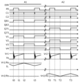
- FIG. 2 shows the polarity instruction signal DIR, the reference pulse signal P0, the first comparison signal C1, the second comparison signal C2, the output signal Q61 of the D flip-flop 61, and the output signal of the D flip-flop 63 in sections A1 and A2 of FIG. 1B.
- It is a graph showing an example of the waveforms of the output signal Q63, the output signal Q71 of the D flip-flop 71, the output signal Q73 of the D flip-flop 73, the drive signals V1 to V4, the current detection voltage Vs, and the motor current IL.
- the horizontal axis in FIG. 2 indicates time.
- 3A and 3B are state diagrams showing the state of each switch element and the current path in sections A1 and A2 of FIG. 1B, respectively.
- the inverted signal of the second reference pulse signal P2 which is a clock input, is fixed at a high level, so the output signal Q63 is maintained at a low level (L). Furthermore, since the second reference pulse signal P2 is at a low level, the output signal Q71 of the D flip-flop 71 having no clock input is maintained at a low level. The output signal Q73 of the D flip-flop 73 whose D terminal receives the inverted signal of the second comparison signal C2 at a high level is also maintained at a low level.
- the drive signal V2 which is the logical sum of the two, is also maintained at a low level, and the second high-side switch element 22 is in an off state and the second low-side switch element 24 is in an on state.
- the first high-side switch element 21 is turned on, a flow flows from the positive electrode of the input power source 1 to the first high-side switch element 21, the motor 3, the second low-side switch element 24, the current detection resistor 4, and the negative electrode of the input power source 1. Since the current increases while oscillating like a surge, the current detection voltage Vs also oscillates, and the first comparison signal C1 also oscillates between a high level and a low level.
- the current detection voltage Vs is ORed with the high level of the first reference pulse signal P1 in the OR circuit 62, and NANDed with the low level of the delayed signal of the delay circuit 78, which will be described later, in the NAND circuit 77. , does not affect circuit operation.
- This state is maintained at least until time t1 when the first reference pulse signal P1 is at a high level, and the motor current IL of the motor 3 to which the power supply voltage is applied in the positive direction increases in the positive direction.
- the pulse duration time of the reference pulse signal P0 is the minimum on-period Tm, which is the minimum value of the mask period.
- the first reference pulse signal P1 falls together with the reference pulse signal P0.
- the current detection voltage Vs has not reached the first reference waveform signal Vr1 and the first comparison signal C1 remains at a high level, so the D flip-flop 61 is not reset and the state is maintained until time t2. be done. That is, each switch element etc. is maintained in the state shown in state diagram (a) in FIG. 3A from time t0 to t2.
- the second high-side switch element 22 is fixed in the off state and the second low-side switch element 24 is fixed in the on state, and the first high-side switch element 22 is fixed in the on state at a predetermined switching period.
- the side switch element 21 and the first low side switch element 23 are alternately turned on and off.
- the on-period of the first high-side switch element 21 is controlled to be longer than the minimum on-period Tm and until the peak value of the motor current IL reaches the target waveform value Vr1/Rs.
- Section A2 in FIG. 1B is a section near the peak value in which the sign of the reference waveform signal is reversed with respect to the above-mentioned section A1, and the operation is performed by switching the roles of the first PWM circuit 6 and the second PWM circuit 7, and as described above.
- the times t0 to t3 of the interval A1 correspond to the times T0 to T3 of the interval A2. That is, the first high-side switch element 21 is fixed in the OFF state, the first low-side switch element 23 is fixed in the ON state, and the second high-side switch element 22 and the second low-side switch element 24 are switched on at a predetermined switching period. Turn on and off alternately.
- the on-period of the second high-side switch element 22 is controlled to be longer than the minimum on-period Tm and until the peak value of the motor current IL reaches the target waveform value Vr2/Rs.
- Each switch element etc. is maintained in the state shown in the state diagram (a) of FIG. 3B from time T0 to T2, and is maintained in the state shown in the state diagram (b) of FIG. 3B from time T2 to T3. be done.
- FIG. 4 shows the polarity instruction signal DIR, the reference pulse signal P0, the first comparison signal C1, the second comparison signal C2, the output signal Q61 of the D flip-flop 61, and the output signal of the D flip-flop 63 in section B of FIG. 1B.
- 7 is a graph showing an example of waveforms of Q63, output signal Q71 of D flip-flop 71, output signal Q73 of D flip-flop 73, drive signals V1 to V4, current detection voltage Vs, and motor current IL.
- FIG. 5 is a state diagram showing the state of each switch element and the path of flowing current in section B of FIG. 1B.
- the first reference pulse signal P1 falls in accordance with the reference pulse signal P0 with the motor current IL exceeding the control target value.
- the D flip-flop 61 is reset and the output signal Q61 falls. Therefore, the drive signal V1 also falls, the first high-side switch element 21 is turned off, and the first low-side switch element 23 is turned on.
- the D flip-flop 73 is clocked at the falling edge of the first reference pulse signal P1 while a high-level signal, which is an inverted signal of the first comparison signal C1, is applied to the D terminal, so that the D flip-flop 73 outputs an output signal.
- the output signal Q73 of the D flip-flop 73 is input to the reset terminal of the D flip-flop 73 via the delay circuit 78 and the NAND circuit 77.
- the output of the delay circuit 78 falls, but since the motor current IL is still higher than the control target value and the inverted signal of the second comparison signal C2 is at a low level, the output of the NAND circuit 77 is The output is maintained at a high level, the D flip-flop 73 is not reset, and the state of each switch element is maintained.
- the level of the first reference waveform signal Vr1 is also low, and when the minimum on-period Tm is reached at time t8 and the reference pulse signal P0 and the first reference pulse signal P1 fall, the motor current IL exceeds the control target value.
- the first high-side switch element 21 is turned off, and the state of each switch element returns to the fast decay state shown in the state diagram (b) of FIG. 5.
- the motor current IL falls below the control target value -Vr2/Rs (the current detection voltage Vs exceeds the second reference waveform signal Vr2), and the second comparison signal C2 falls.
- the delayed signal of the output signal Q73 of the D flip-flop 73 has not arrived, so the state remains unchanged.
- the D flip-flop 73 is reset and the output signal Q73 falls, the second high-side switch element 22 is turned off, and each switch The state of the element returns to the slow decay state shown in FIG. 5 (c). That is, the delay time of the output signal Q73 of the D flip-flop 73 by the delay circuit 78 is the minimum period of the fast decay state. Thereafter, such operations are repeated, and the motor current IL converges to the target waveform.
- FIG. 6 shows the polarity instruction signal DIR, the reference pulse signal P0, the first comparison signal C1, the second comparison signal C2, the output signal Q61 of the D flip-flop 61, and the output signal of the D flip-flop 63 in the section C of FIG. 1B.
- 7 is a graph showing an example of waveforms of Q63, output signal Q71 of D flip-flop 71, output signal Q73 of D flip-flop 73, drive signals V1 to V4, current detection voltage Vs, and motor current IL.
- Section C is a region where the polarity instruction signal DIR changes from a high level to a low level and the motor current IL should cross zero, and the first reference waveform signal Vr1 and the second reference waveform signal Vr2 are approximately zero.
- the drive signal V1 also rises, and the first high-side switch element 21 is turned on.
- the drive signal V2 falls and the first low-side switch element 23 is turned off. Since the first reference waveform signal Vr1 and the second reference waveform signal Vr2 are approximately zero, the first comparison signal C1 and the second comparison signal C2 are at a low level.
- the D flip-flop 61 is reset and the drive signal V1 becomes low level together with the output signal Q61, and the first high-side switch element 21 is turned off, and the first low-side switch element 23 is turned on.
- the D flip-flop 73 is clocked by the falling edge of the first reference pulse signal P1, and raises the output signal Q73.
- the drive signal V2 also becomes high level
- the second high-side switch element 22 is turned on
- the second low-side switch element 24 is turned off.
- the state of each switch element shifts from the state shown in FIG. 5 (a) to the fast decay state shown in state diagram (b).
- the motor current IL decreases, the current detection voltage Vs becomes negative, and the first comparison signal C1 and the second comparison signal C2 become high level.
- the time t13 is set to be after the delay time of the delay circuit 78, there is a possibility that the motor current IL reaches zero first, and then the delay time passes and the state of each switch element shifts to the slow decay state. . In that case, the motor current IL flows in a negative direction, but the motor current IL attenuates in a slow decay state. Although it depends on the characteristics and state of the motor 3, it is assumed that the back electromotive voltage is small near the zero cross, and the motor current IL in the slow decay state is also attenuated to zero or a small value.
- the first comparison signal C1 and the second comparison signal C2 are undefined.
- the first comparison signal C1 and the second comparison signal C2 are not referred to, and there is no effect on the operation. If it is desired to avoid this undefined state, hysteresis or offset may be set in the first comparison circuit 55 and the second comparison circuit 56.
- the state changes so that the first reference pulse signal P1 is fixed at a low level and the reference pulse signal P0 is output as the second reference pulse signal P2.
- the clock is input to the D flip-flop 71, the output signal Q71 rises, and the drive signal V2 rises via the OR circuits 70 and 76. Therefore, the second high-side switch element 22 is turned on and the second low-side switch element 24 is turned off. Power supply voltage Vcc is applied to the motor 3 in the negative direction, and the motor current IL increases in the negative direction.
- the second high-side switch element 22 is turned off, the first high-side switch element 21 is turned on, and the state of each switch element changes to fast decay, and at time t17, the first high-side switch element 22 turns off.
- the switch element 21 turns off and enters a slow decay state.
- the above operation differs in that the role is transferred from the first PWM circuit 6 to the second PWM circuit 7, but it is the same operation as described above, and the motor current IL smoothly reverses polarity. go.
- the motor current IL supplied from the input power source 1 is detected and the first target waveform value Vr1/Rs is set in the positive direction, and the first target waveform value Vr1/Rs is set in the negative direction.
- the peak current control to follow the target waveform value Vr2/Rs of 2
- the target current when the target current is exceeded during the minimum on period Tm, by providing a period in which the fast decay state occurs until the current decreases to the target current, the target current can be maintained even near the zero cross.
- the current waveform can be maintained.
- the motor drive device according to the present embodiment differs from the motor drive device 10 according to the first embodiment mainly in that the reference waveform generation circuit generates only one reference waveform signal.
- the motor drive device according to the present embodiment will be described below with reference to FIGS. 7A to 10, focusing on the differences from the motor drive device 10 according to the first embodiment.
- FIG. 7A is a circuit configuration diagram of motor drive device 110 according to this embodiment.
- the same components as in FIG. 1A are given the same reference numerals, and their description will be omitted.
- the motor drive device 110 includes a first series switch circuit 31, a second series switch circuit 32, a reference pulse generation circuit 50, and a current detection resistor 4. , a PWM circuit 5A, a reference waveform generation circuit 51A, and a current comparison circuit 57.
- motor drive device 110 further includes an amplifier 40, resistors 41, 42, 44, and 45, and a switch 43.
- the reference waveform generation circuit 51A generates a reference waveform signal Vr with a signal level of 0 or more.
- the reference waveform signal Vr will be explained using FIG. 7B.
- FIG. 7B is a graph showing an example of the waveforms of the polarity instruction signal DIR and the reference waveform signal Vr according to the present embodiment.
- Graph (a) in FIG. 7B is a graph showing an example of the waveform of the polarity instruction signal DIR.
- Graph (b) in FIG. 7B is a graph showing an example of the waveform of the reference waveform signal Vr.
- the horizontal axis of each graph represents time.
- the reference waveform signal Vr maintains a signal level of 0 or more and does not include a negative signal.
- the PWM circuit 5A includes a first switching circuit 58 and a second switching circuit 59 in addition to the same circuits as the first PWM circuit 6 according to the first embodiment.
- the PWM circuit 5A receives a reference pulse signal P0 instead of the first reference pulse signal P1 and the second reference pulse signal P2 according to the first embodiment. Further, the PWM circuit 5A does not include the OR circuit 66, and the output of the OR circuit 60 and the output signal Q63 of the D flip-flop 63 are input to the first switching circuit 58 and the second switching circuit 59.
- the first switching circuit 58 outputs the first drive signal to the first series switch circuit 31 mainly during a first period in which the motor current IL flows from the first connection point X1 to the second connection point X2. , is a circuit that outputs an output to the second series switch circuit 32 mainly during the second period when the motor current IL flows from the second connection point X2 to the first connection point X1.
- the first switching circuit 58 receives the polarity instruction signal DIR from the reference waveform generation circuit 51A, the output signal of the OR circuit 60, and the output signal Q63 of the D flip-flop 63, and selects the polarity instruction signal DIR according to the polarity instruction signal DIR.
- the output signal of the OR circuit 60 or the output signal Q63 of the D flip-flop 63 is output to the serial switch circuit 31 of No. 1.
- the second switching circuit 59 outputs the second drive signal to the second series switch circuit 32 mainly during the first period in which the motor current IL flows from the first connection point X1 to the second connection point X2.
- the second switching circuit 59 receives the polarity instruction signal DIR from the reference waveform generation circuit 51A, the output signal of the OR circuit 60, and the output signal Q63 of the D flip-flop 63, and selects the polarity instruction signal DIR according to the polarity instruction signal DIR.
- the output signal of the OR circuit 60 or the output signal Q63 of the D flip-flop 63 is output to the serial switch circuit 31 of No. 1.
- the output of the OR circuit 60 of the PWM circuit 5A becomes the drive signal V1 via the first switching circuit 58 when the polarity instruction signal DIR is at a high level, and becomes the drive signal V1 via the first switching circuit 58 when the polarity instruction signal DIR is at a low level. 59 to become the drive signal V2.
- the output signal Q63 of the D flip-flop 63 becomes the drive signal V2 via the second switching circuit 59, and when the polarity instruction signal DIR is at a low level, it becomes the drive signal V2 through the first switching circuit. 58 to become the drive signal V1.
- the objects to be compared in the current comparison circuit 57 are also different from those in the first embodiment.
- the current detection voltage Vs of the current detection resistor 4 and the first reference waveform signal Vr1 were compared, but in this embodiment, the reference waveform signal Vr is once amplified N times by the amplifier 40, and then the current detection voltage Vs of the current detection resistor 4 is compared with the first reference waveform signal Vr1. and the resistor 42 and return it to the reference waveform signal Vr, which is then input to the current comparison circuit 57.
- the detection voltage VsA obtained from the voltage Vs of the current detection resistor 4 via the resistor 45 having a resistance value R5 is input to the current comparison circuit 57, and is compared with the reference waveform signal (divided voltage) Vr to generate a comparison signal C3. is output. Furthermore, a series circuit of a switch 43 that opens and closes in response to the output signal Q63 of the D flip-flop 63 and a resistor 44 having a resistance value R4 is connected between the output of the amplifier 40 (voltage N ⁇ Vr) and a resistor 45 (voltage VsA). be done.
- the comparison signal C3 output by the current comparison circuit 57 is the comparison result between the current detection voltage Vs and the reference waveform signal Vr.
- the switch 43 when the output signal Q63 of the D flip-flop 63 is at a high level, that is, in the fast decay state, the switch 43 is in the on state, and the detection voltage VsA is biased by the output N ⁇ Vr of the amplifier 40, as shown in the following equation. become.
- VsA (R4 ⁇ Vs+R5 ⁇ N ⁇ Vr)/(R4+R5)
- Vs ⁇ 1-(N-1) ⁇ R5/R4 ⁇ Vr
- the current comparison circuit 57 Equivalently, the current detection voltage Vs (that is, the current signal) is compared with a signal obtained by negatively inverting the reference waveform signal Vr.
- FIG. 8 shows the polarity instruction signal DIR, reference pulse signal P0, comparison signal C3, output signal Q61 of the D flip-flop 61, output signal Q63 of the D flip-flop 63, drive signals V1 to V4, in the sections A1 and A2 of FIG. 7B, It is a graph showing an example of waveforms of current detection voltage Vs and motor current IL. The state of each switch element and the path of the flowing current are the same as in FIGS. 3A and 3B. The operation near the reference waveform peak will be described below with reference to FIGS. 7A, 7B, and 8.
- the drive signal V1 When the polarity instruction signal DIR is at a high level, that is, the motor current IL is in the positive direction, and the reference pulse signal P0 rises at time t0, the drive signal V1 also rises via the OR circuit 60 and the first switching circuit 58. The first high-side switch element 21 is turned on. At the same time, the drive signal V2 falls and the first low-side switch element 23 is turned off. Since the reference pulse signal P0 is clocked into the D flip-flop 61 while the high-level comparison signal C3 is input to the reset terminal, the output signal Q61 of the D flip-flop 61 also rises.
- the output signal Q63 of the D flip-flop 63 which receives the inverted signal of the comparison signal C3 at a high level and is input to the D terminal, is at a low level, and the output signal Q63 becomes the drive signal V2 via the second switching circuit 59. Therefore, the second high-side switch element 22 is in an off state, and the second low-side switch element 24 is in an on state.
- the positive electrode of the input power source 1 is connected to the first high-side switch element 21, the motor 3, the second low-side switch element 24, the current detection resistor 4, and the negative electrode of the input power source 1.
- the current detection voltage Vs Since the flowing current increases while oscillating like a surge, the current detection voltage Vs also oscillates, and the comparison signal C3 also oscillates between a high level and a low level. However, the current detection voltage Vs is logically summed with the high level of the reference pulse signal P0 in the OR circuit 62, and NANDed with the low level of the delayed signal of the delay circuit 68, which will be described later, in the NAND circuit 67, so that the circuit operates. does not affect. This state is maintained at least until time t1 when the reference pulse signal P0 is at a high level, and the motor current IL of the motor 3 to which the power supply voltage is applied in the positive direction increases in the positive direction. As described above, the pulse duration time of the reference pulse signal P0 is the minimum on-period Tm, which is the minimum value of the mask period.
- the reference pulse signal P0 falls.
- the current detection voltage Vs has not reached the reference waveform signal Vr and the comparison signal C3 remains at a high level, so the D flip-flop 61 is not reset and the state is maintained until time t2.
- Each switch element etc. is maintained in the state shown in the state diagram (a) of FIG. 3A from time t0 to t2.
- the second high-side switch element 22 is fixed in the OFF state
- the second low-side switch element 24 is fixed in the ON state
- the first high-side switch element 22 is fixed in the ON state at a predetermined switching period.
- 21 and the first low-side switch element 23 are alternately turned on and off.
- the on-period of the first high-side switch element 21 is controlled to be longer than the minimum on-period Tm and until the peak value of the motor current IL reaches the target waveform value Vr/Rs.
- the PWM circuit 5A operates in the same manner as in section A1 described above, but since the polarity instruction signal DIR is at a low level, the states of the first switching circuit 58 and the second switching circuit 59 are different from those in the section A1.
- the output signal of the OR circuit 60 is the drive signal V2
- the output signal Q63 of the D flip-flop 63 is the drive signal V1.
- the time T0 to T3 of the section A2 corresponds to the time t0 to t3 of the above-mentioned section A1, and the first high side switch element 21 is fixed in the off state and the first low side switch element 23 is fixed in the on state, and a predetermined switching is performed.
- the second high-side switch element 22 and the second low-side switch element 24 are alternately turned on and off in cycles.
- the on period of the second high side switch element 22 is controlled to be longer than the minimum on period Tm and until the peak value of the motor current IL reaches the target waveform value Vr/Rs.
- Each switch element, etc. is maintained in the state shown in the state diagram (a) of FIG. 3B from time T0 to T2, and is maintained in the state shown in state diagram (b) of FIG. 3B from time T2 to T3.
- FIG. 9 shows the polarity instruction signal DIR, reference pulse signal P0, comparison signal C3, output signal Q61 of the D flip-flop 61, output signal Q63 of the D flip-flop 63, drive signals V1 to V4, and current detection in section B of FIG. 7B. It is a graph which shows an example of the waveform of voltage Vs and motor current IL. The state of each switch element and the path of the flowing current are similar to the state diagram shown in FIG. 5.
- the reference pulse signal P0 falls in accordance with the reference pulse signal P0 with the motor current IL exceeding the control target value Vr/Rs.
- the D flip-flop 61 is reset and the output signal Q61 falls. Therefore, the drive signal V1 also falls, the first high-side switch element 21 is turned off, and the first low-side switch element 23 is turned on. Further, the D flip-flop 63 is clocked at the falling edge of the reference pulse signal P0 while a high level signal, which is an inverted signal of the comparison signal C3, is input to the D terminal, so that the output signal Q63 rises.
- each switch element is the fast decay state shown in the state diagram (b) of FIG. 5, in which the current supplied from the input power source 1 and flowing through the current detection resistor 4 flows backward and becomes a regenerative current. Further, when the output signal Q63 of the D flip-flop 63 becomes high level, the switch 43 is turned on, and the comparison signal C3 becomes equivalently the result of comparison between the current detection voltage Vs and the negative reference waveform signal -Vr.
- the output signal Q63 of the D flip-flop 63 is input to the reset terminal of the D flip-flop 63 via the delay circuit 68 and the NAND circuit 67.
- the output of the delay circuit 68 falls, but since the motor current IL is still higher than the control target value and the inverted signal of the comparison signal C3 is at a low level, the output of the NAND circuit 67 is at a high level.
- the D flip-flop 63 is not reset and the state of the switch is maintained.
- the drive signal V1 When the reference pulse signal P0 rises at time t7, the drive signal V1 also rises via the OR circuit 60 and the first switching circuit 58, and the first high-side switch element 21 is turned on. At the same time, the drive signal V3 falls, the first low-side switch element 23 turns off, and the motor current IL of the motor 3 to which the power supply voltage Vcc is applied in the positive direction increases in the positive direction (state diagram in FIG. 5). (a)). Compared to the previous cycle, the motor current IL is attenuated due to the fast decay state, and the level of the current detection voltage Vs is also lowered.
- the D flip-flop 63 is reset and the output signal Q63 falls, and the second high-side switch element 22 is turned off and slow decays. state. That is, the delay time of the output signal Q63 of the D flip-flop 63 by the delay circuit 68 is the minimum period of the fast decay state. Thereafter, such operations are repeated, and the motor current IL converges to the target waveform.
- FIG. 10 shows the polarity instruction signal DIR, reference pulse signal P0, comparison signal C3, output signal Q61 of the D flip-flop 61, output signal Q63 of the D flip-flop 63, drive signals V1 to V4, and current detection in section C of FIG. 7B. It is a graph which shows an example of the waveform of voltage Vs and motor current IL.
- Section C is a region where the polarity instruction signal DIR changes from a high level to a low level and the motor current IL should cross zero, and the reference waveform signal Vr is approximately zero.
- the D flip-flop 61 is reset and the drive signal V1 becomes low level together with the output signal Q61, and the first high-side switch element 21 is turned off. state, and the first low-side switch element 23 is turned on.
- the D flip-flop 63 is clocked by the falling edge of the reference pulse signal P0, and raises the output signal Q63.
- the drive signal V2 also becomes high level, the second high-side switch element 22 is turned on, and the second low-side switch element 24 is turned off.
- time t13 is set after the delay time of the delay circuit 68, there may be a case where the motor current IL reaches zero first, and then the delay time passes and the state of the switch shifts to the slow decay state. In that case, the motor current IL flows in the negative direction, but the current attenuates in a slow decay state. Although it depends on the characteristics and state of the motor 3, it is assumed that the back electromotive voltage is small near the zero cross, and the motor current in the slow decay state is also attenuated to zero or a small value.
- the comparison signal C3 becomes undefined.
- the comparison signal C3 is not referred to, and there is no effect on the operation. If it is desired to avoid this unstable state, hysteresis or offset may be set in the current comparison circuit 57.
- the second high-side switch element 22 turns off, the first high-side switch element 21 turns on, and enters the fast decay state, and at time t17, the first high-side switch element 21 turns off. state and turns into a slow decay state.
- the polarity of the motor current IL is smoothly reversed.
- the motor current IL supplied from the input power source 1 is detected, and the target waveform value Vr/Rs is detected in the positive direction, and the target waveform value -
- the target current waveform is maintained even near zero cross by providing a period in which the current is in a fast decay state until it decreases to the target current. be able to.
- fast decay may be used instead of slow decay in normal operation, but fast decay increases the ripple of the motor current.
- An increase in ripple current leads to an increase in conduction loss and an increase in switching frequency noise due to an increase in the effective value of the current. Therefore, in the present disclosure, the fast decay state is provided only to correct the excess of the current target value during the minimum on-period.
- the high level and low level of each signal may be inverted, and the circuit configuration may be changed depending on each signal.
- the motor drive device of the present disclosure can be applied to motors for various uses including in-vehicle use, as a motor drive device that can drive a motor with low noise and low vibration, for example.
Abstract
A motor drive device (10) comprises: a reference pulse generation circuit (50) that generates a reference pulse signal; a current detection unit that outputs a current signal corresponding to the motor current; a reference waveform generation circuit (51) that generates a reference waveform signal; a current comparison circuit (8) that compares the current signal and the reference waveform signal; and a PWM circuit (5) that outputs a first drive signal and a second drive signal. The first drive signal includes a first pulse that starts synchronously with the start of the reference pulse signal and ends when the absolute value of the current signal has exceeded the absolute value of the reference waveform signal after a pulse continuation time has elapsed since the beginning of the reference pulse signal. In a case in which the absolute value of the current signal has exceeded the absolute value of the reference waveform signal within the pulse continuation time, the second drive signal includes a second pulse that starts after the end of the first pulse and is continued at least for a period until the absolute value of the current signal falls below the absolute value of the reference waveform signal.
Description
本開示は、モータ駆動装置に関するものである。
The present disclosure relates to a motor drive device.
モータ駆動装置において、低騒音、低振動が要求されている。低騒音、低振動でモータを駆動するモータ駆動装置には、例えば特許文献1に開示されているようなものがある。特許文献1のモータ駆動装置は、スイッチ素子のスイッチング動作によってモータコイルに流れる電流を抵抗で検出し、その検出電圧のピーク値が、基準電圧に追従するように当該電流をPWM(Pulse Width Modulation:パルス幅変調)制御することによって、低騒音、低振動を実現しようとしている。ここで、基準電圧とは、モータコイルに流れる電流の目標値を設定する電圧である。
Low noise and low vibration are required in motor drive devices. BACKGROUND ART Examples of motor drive devices that drive a motor with low noise and low vibration include one disclosed in Patent Document 1, for example. The motor drive device disclosed in Patent Document 1 uses a resistor to detect the current flowing through the motor coil due to the switching operation of a switch element, and applies PWM (Pulse Width Modulation) to the current so that the peak value of the detected voltage follows a reference voltage. The aim is to achieve low noise and vibration through pulse width modulation (pulse width modulation) control. Here, the reference voltage is a voltage that sets a target value of the current flowing through the motor coil.
上記従来技術では、スイッチ素子のターンオン時のサージ電流を無視する期間、つまり、PWM制御を停止する期間であるマスク期間が必要である。このマスク期間は、サージ電流が発生し得る期間をカバーするのに十分な長さの期間である最小オン期間に設定される必要があるため、所定の時間以下に短縮することができない。このようなマスク期間を設けることによって、モータコイルに流れる電流がゼロとなるゼロクロスポイント近傍で電流が目標値を越え得る。このため、特許文献1においてもゼロクロスポイント近傍ではスイッチング動作モードの切り換えによる対策が開示されている。しかしながらスイッチ素子の特性によって最小オン期間の設定は異なり、スイッチ素子駆動回路の汎用性から最小オン期間は余裕をもって長めに設定されるため、ゼロクロスポイント近傍で電流波形が目標波形から外れてしまうといった上記問題点は顕著となる。
The above conventional technology requires a mask period, which is a period in which the surge current when the switch element is turned on is ignored, that is, a period in which PWM control is stopped. This mask period cannot be shortened below a predetermined time because it must be set to a minimum on period that is long enough to cover the period during which a surge current may occur. By providing such a mask period, the current can exceed the target value near the zero cross point where the current flowing through the motor coil becomes zero. For this reason, Patent Document 1 also discloses a countermeasure by switching the switching operation mode near the zero-crossing point. However, the setting of the minimum on-period differs depending on the characteristics of the switch element, and the minimum on-period is set to be long with some margin due to the versatility of the switch element drive circuit, so the current waveform deviates from the target waveform near the zero-crossing point. The problem becomes obvious.
本開示は、このような課題を解決するものであり、ゼロクロスポイント近傍における電流波形を目標波形に正確に追従させることができるモータ駆動装置を提供する。
The present disclosure solves these problems and provides a motor drive device that can cause a current waveform near a zero-crossing point to accurately follow a target waveform.
以上に鑑み、本開示に係るモータ駆動装置は、モータを駆動するモータ駆動装置であって、第1のハイサイドスイッチ素子、及び第1のローサイドスイッチ素子を含む第1の直列スイッチ回路と、第2のハイサイドスイッチ素子、及び第2のローサイドスイッチ素子を含み、前記第1の直列スイッチ回路に並列接続される第2の直列スイッチ回路と、ゼロより大きいパルス継続時間を有する基準パルス信号を所定の周期で生成する基準パルス生成回路と、前記モータに流れる電流であるモータ電流に対応する電流信号を出力する電流検出部と、前記モータ電流の制御目標値に対応する基準波形信号を生成する基準波形生成回路と、前記電流信号と前記基準波形信号とを比較して比較信号を生成する電流比較回路と、前記基準パルス信号、前記基準波形信号、及び前記比較信号が入力され、第1の駆動信号、及び第2の駆動信号を出力するPWM回路と、を有し、前記第1のハイサイドスイッチ素子と前記第1のローサイドスイッチ素子との接続点である第1の接続点と、前記第2のハイサイドスイッチ素子と前記第2のローサイドスイッチ素子との接続点である第2の接続点と、の間に前記モータが接続され、前記第1の駆動信号は、前記基準パルス信号の開始と同期して開始される第1のパルスであって、前記基準パルス信号の先頭から前記パルス継続時間の経過後であって前記電流信号の絶対値が前記基準波形信号の絶対値を越えた時に終了される第1のパルスを含み、前記第2の駆動信号は、前記パルス継続時間以内に前記電流信号の絶対値が前記基準波形信号の絶対値を越えた場合に、前記第1のパルスの終了後に開始される第2のパルスであって、少なくとも前記電流信号の絶対値が前記基準波形信号の絶対値を下回るまでの期間は持続される前記第2のパルスを含み、前記PWM回路は、主として前記第1の接続点から前記第2の接続点へ前記モータ電流が流れる第1の期間において、前記第1の駆動信号を前記第1の直列スイッチ回路に出力し、前記第2の駆動信号を前記第2の直列スイッチ回路に出力し、主として前記第2の接続点から前記第1の接続点へ前記モータ電流が流れる第2の期間において、前記第2の駆動信号を前記第1の直列スイッチ回路に出力し、前記第1の駆動信号を前記第2の直列スイッチ回路に出力する。
In view of the above, a motor drive device according to the present disclosure is a motor drive device that drives a motor, and includes a first series switch circuit including a first high side switch element and a first low side switch element, and a first series switch circuit including a first high side switch element and a first low side switch element. a second series switch circuit including a second high-side switch element and a second low-side switch element and connected in parallel to the first series switch circuit, and a reference pulse signal having a pulse duration greater than zero; a reference pulse generation circuit that generates a reference pulse with a period of , a current detection unit that outputs a current signal corresponding to a motor current that is a current flowing through the motor, and a reference that generates a reference waveform signal that corresponds to a control target value of the motor current. a waveform generation circuit; a current comparison circuit that compares the current signal and the reference waveform signal to generate a comparison signal; the reference pulse signal, the reference waveform signal, and the comparison signal are input; a PWM circuit that outputs a signal and a second drive signal, and a first connection point that is a connection point between the first high-side switch element and the first low-side switch element; The motor is connected between a second connection point that is a connection point between the second high-side switch element and the second low-side switch element, and the first drive signal is connected to the start of the reference pulse signal. a first pulse that is started in synchronization with the reference pulse signal, when the absolute value of the current signal exceeds the absolute value of the reference waveform signal after the pulse duration has elapsed from the beginning of the reference pulse signal; the second drive signal includes a first pulse that is terminated, and the second drive signal is configured to terminate the first pulse if the absolute value of the current signal exceeds the absolute value of the reference waveform signal within the pulse duration. The PWM circuit includes a second pulse that is started after the end of the pulse and is continued for at least a period until the absolute value of the current signal becomes lower than the absolute value of the reference waveform signal, and the PWM circuit includes: During a first period in which the motor current mainly flows from the first connection point to the second connection point, the first drive signal is output to the first series switch circuit, and the second drive signal is output to the first series switch circuit. is output to the second series switch circuit, and during a second period in which the motor current mainly flows from the second connection point to the first connection point, the second drive signal is output to the first series switch circuit. and outputs the first drive signal to the second series switch circuit.
本開示によれば、ゼロクロスポイント近傍における電流波形を目標波形に正確に追従させることができるモータ駆動装置を提供できる。
According to the present disclosure, it is possible to provide a motor drive device that can cause a current waveform near a zero-crossing point to accurately follow a target waveform.
以下、本開示の実施の形態について、図面を参照しながら説明する。なお、以下に説明する実施の形態は、いずれも本開示の一具体例を示すものである。したがって、以下の実施の形態で示される、数値、形状、材料、構成要素、及び、構成要素の配置位置や接続形態などは、一例であって本開示を限定する主旨ではない。
Hereinafter, embodiments of the present disclosure will be described with reference to the drawings. Note that the embodiments described below each represent a specific example of the present disclosure. Therefore, the numerical values, shapes, materials, components, arrangement positions and connection forms of the components shown in the following embodiments are merely examples and do not limit the present disclosure.
また、各図は模式図であり、必ずしも厳密に図示されたものではない。したがって、各図において縮尺等は必ずしも一致していない。なお、各図において、実質的に同一の構成に対しては同一の符号を付しており、重複する説明は省略又は簡略化する。
Furthermore, each figure is a schematic diagram and is not necessarily strictly illustrated. Therefore, the scale etc. in each figure are not necessarily the same. In addition, in each figure, the same code|symbol is attached to the substantially the same structure, and the overlapping description is omitted or simplified.
(実施の形態1)
実施の形態1に係るモータ駆動装置について説明する。まず、本実施の形態に係るモータ駆動装置の回路構成について、図1Aを用いて説明する。図1Aは、本実施の形態に係るモータ駆動装置10の回路構成図である。図1Aには、モータ駆動装置10が駆動するモータ3、モータ駆動装置10に直流電力を供給する入力電源1も併せて示されている。 (Embodiment 1)
A motor drive device according toEmbodiment 1 will be described. First, the circuit configuration of the motor drive device according to this embodiment will be explained using FIG. 1A. FIG. 1A is a circuit configuration diagram of a motor drive device 10 according to the present embodiment. FIG. 1A also shows a motor 3 driven by the motor drive device 10 and an input power source 1 that supplies DC power to the motor drive device 10.
実施の形態1に係るモータ駆動装置について説明する。まず、本実施の形態に係るモータ駆動装置の回路構成について、図1Aを用いて説明する。図1Aは、本実施の形態に係るモータ駆動装置10の回路構成図である。図1Aには、モータ駆動装置10が駆動するモータ3、モータ駆動装置10に直流電力を供給する入力電源1も併せて示されている。 (Embodiment 1)
A motor drive device according to
図1Aに示されるように、入力電源1は、電源ラインとグランドラインとの間に電源電圧Vccを供給する。入力電源1は、例えば、バッテリである。
As shown in FIG. 1A, the input power supply 1 supplies a power supply voltage Vcc between a power supply line and a ground line. The input power source 1 is, for example, a battery.
モータ駆動装置10は、モータ3を駆動する装置である。モータ駆動装置10は、第1の直列スイッチ回路31と、第2の直列スイッチ回路32と、基準パルス生成回路50と、電流検出抵抗4と、PWM回路5と、基準波形生成回路51と、電流比較回路8と、を有する。
The motor drive device 10 is a device that drives the motor 3. The motor drive device 10 includes a first series switch circuit 31, a second series switch circuit 32, a reference pulse generation circuit 50, a current detection resistor 4, a PWM circuit 5, a reference waveform generation circuit 51, and a current It has a comparison circuit 8.
第1の直列スイッチ回路31は、第1のハイサイドスイッチ素子21、及び第1のローサイドスイッチ素子23を含む直列回路である。第1のハイサイドスイッチ素子21と、第1のローサイドスイッチ素子23とは、第1の接続点X1で直列に接続されている。第1の接続点X1は、第1のハイサイドスイッチ素子21と第1のローサイドスイッチ素子23との接続点である。本実施の形態では、第1の直列スイッチ回路31は、反転器25をさらに有する。反転器25は、第1のローサイドスイッチ素子23の制御端子と、第1のハイサイドスイッチ素子21の制御端子との間に接続され、第1のハイサイドスイッチ素子21の制御端子に入力される駆動信号V1の反転信号である駆動信号V3を第1のローサイドスイッチ素子23の制御端子に入力する。
The first series switch circuit 31 is a series circuit including a first high-side switch element 21 and a first low-side switch element 23. The first high-side switch element 21 and the first low-side switch element 23 are connected in series at a first connection point X1. The first connection point X1 is a connection point between the first high-side switch element 21 and the first low-side switch element 23. In this embodiment, the first series switch circuit 31 further includes an inverter 25. The inverter 25 is connected between the control terminal of the first low-side switch element 23 and the control terminal of the first high-side switch element 21, and is input to the control terminal of the first high-side switch element 21. A drive signal V3, which is an inverted signal of the drive signal V1, is input to the control terminal of the first low-side switch element 23.
第2の直列スイッチ回路32は、第2のハイサイドスイッチ素子22、及び第2のローサイドスイッチ素子24を含み、第1の直列スイッチ回路31に並列接続される直列回路である。第2のハイサイドスイッチ素子22と、第2のローサイドスイッチ素子24とは、第2の接続点X2で直列に接続されている。第2の接続点X2は、第2のハイサイドスイッチ素子22と第2のローサイドスイッチ素子24との接続点である。第1のハイサイドスイッチ素子21と、第2のハイサイドスイッチ素子22とは、電源ラインで接続され、第1のローサイドスイッチ素子23と、第2のローサイドスイッチ素子24とは、接続される。本実施の形態では、第2の直列スイッチ回路32は、反転器26をさらに有する。反転器26は、第2のローサイドスイッチ素子24の制御端子と、第2のハイサイドスイッチ素子22の制御端子との間に接続され、第2のハイサイドスイッチ素子22の制御端子に入力される駆動信号V2の反転信号である駆動信号V4を第2のローサイドスイッチ素子24の制御端子に入力する。
The second series switch circuit 32 is a series circuit that includes a second high-side switch element 22 and a second low-side switch element 24 and is connected in parallel to the first series switch circuit 31. The second high-side switch element 22 and the second low-side switch element 24 are connected in series at a second connection point X2. The second connection point X2 is a connection point between the second high-side switch element 22 and the second low-side switch element 24. The first high-side switch element 21 and the second high-side switch element 22 are connected by a power supply line, and the first low-side switch element 23 and the second low-side switch element 24 are connected. In this embodiment, the second series switch circuit 32 further includes an inverter 26. The inverter 26 is connected between the control terminal of the second low-side switch element 24 and the control terminal of the second high-side switch element 22, and is input to the control terminal of the second high-side switch element 22. A drive signal V4, which is an inverted signal of the drive signal V2, is input to the control terminal of the second low-side switch element 24.
第1のハイサイドスイッチ素子21、第2のハイサイドスイッチ素子22、第1のローサイドスイッチ素子23、及び第2のローサイドスイッチ素子24の構成は特に限定されない。各スイッチ素子として、例えば、NチャネルMOSFETを用いることができる。なお、各スイッチ素子の制御端子に入力される信号を反転することで、各スイッチ素子としてPチャネルMOSFETを用いることも可能である。本開示では、ボディダイオードを有し、制御端子に高レベル(つまり、Hレベル)の駆動信号が印加されると第1端子-第2端子間が導通してON状態になる理想スイッチとして、各スイッチ素子を説明する。
The configurations of the first high-side switch element 21, the second high-side switch element 22, the first low-side switch element 23, and the second low-side switch element 24 are not particularly limited. For example, an N-channel MOSFET can be used as each switch element. Note that it is also possible to use a P-channel MOSFET as each switch element by inverting the signal input to the control terminal of each switch element. In the present disclosure, each of the ideal switches has a body diode, and when a high level (that is, H level) drive signal is applied to the control terminal, conduction occurs between the first terminal and the second terminal and turns on. The switch element will be explained.
第1の直列スイッチ回路31と第2の直列スイッチ回路32とを含むブリッジ回路の第1の接続点X1と第2の接続点X2との間にモータ3が接続される。
The motor 3 is connected between a first connection point X1 and a second connection point X2 of a bridge circuit including a first series switch circuit 31 and a second series switch circuit 32.
電流検出抵抗4は、モータ3に流れる電流であるモータ電流ILに対応する電流信号を出力する電流検出部の一例である。本実施の形態では、電流検出抵抗4は、第1のローサイドスイッチ素子23、及び第2のローサイドスイッチ素子24の接続点と、グランドラインとの間に接続される抵抗素子である。以下では、電流検出抵抗4の抵抗値をRsと表す。
The current detection resistor 4 is an example of a current detection unit that outputs a current signal corresponding to the motor current IL, which is the current flowing through the motor 3. In this embodiment, the current detection resistor 4 is a resistance element connected between the connection point of the first low-side switch element 23 and the second low-side switch element 24 and the ground line. Below, the resistance value of the current detection resistor 4 will be expressed as Rs.
以上のように、電源ラインとグランドラインとの間には、第1の直列スイッチ回路31と第2の直列スイッチ回路32とを含むブリッジ回路と、モータ3と、電流検出抵抗4とが接続される。
As described above, the bridge circuit including the first series switch circuit 31 and the second series switch circuit 32, the motor 3, and the current detection resistor 4 are connected between the power supply line and the ground line. Ru.
上記のような駆動信号V1~V4によると各ハイサイドスイッチ素子と各ローサイドスイッチ素子とは交互にオンオフするが、実際にはスイッチングの際に同時導通となる電源地絡を防ぐために、各ハイサイドスイッチ素子と各ローサイドスイッチ素子とがともにオフ状態となる期間であるデッドタイムと称される期間が設けられる。あるいは、各ハイサイドスイッチ素子と各ローサイドスイッチ素子とがともにオフ状態となる期間を設ける動作モードもある。しかしながら、このような動作は、周知技術であって本開示での要諦ではない。このため、本開示では、説明が煩雑となることを回避するために、このような動作の図示や説明は省略し、各ハイサイドスイッチ素子と各ローサイドスイッチ素子とは同時に、かつ交互にオンオフするとして説明する。
According to the drive signals V1 to V4 as described above, each high-side switch element and each low-side switch element are turned on and off alternately, but in reality, each high-side switch element and each low-side switch element are turned on and off alternately. A period called a dead time is provided, which is a period during which both the switch element and each low-side switch element are in an off state. Alternatively, there is also an operation mode that provides a period in which each high-side switch element and each low-side switch element are both in an OFF state. However, such operation is a well-known technique and is not the gist of the present disclosure. Therefore, in the present disclosure, in order to avoid complicating the explanation, illustrations and explanations of such operations are omitted, and each high-side switch element and each low-side switch element are turned on and off simultaneously and alternately. It will be explained as follows.
基準パルス生成回路50は、ゼロより大きいパルス継続時間(つまり、パルス幅)を有する基準パルス信号P0を所定の周期で生成する回路である。このパルス継続時間を最小オン期間とも称する。パルス継続時間、所定の周期は特に限定されない。本実施の形態では、パルス継続時間は、2μ秒であり、所定の周期は、10μ秒である。
The reference pulse generation circuit 50 is a circuit that generates a reference pulse signal P0 having a pulse duration (that is, pulse width) greater than zero at a predetermined period. This pulse duration is also referred to as the minimum on-period. The pulse duration and the predetermined period are not particularly limited. In this embodiment, the pulse duration is 2 microseconds and the predetermined period is 10 microseconds.
基準波形生成回路51は、モータ電流ILの制御目標値に対応する基準波形信号を生成する回路である。本実施の形態では、基準波形信号は、第1の基準波形信号と、第2の基準波形信号と、を含む。モータ3の回転位置に応じて、第1の接続点X1から第2の接続点X2へ向かう向き(以後、正向きとも称する)に流れるモータ電流ILの制御目標波形となる第1の基準波形信号Vr1と、第2の接続点X2から第1の接続点X1へ向かう向き(以後、負向きとも称する)に流れるモータ電流の制御目標波形である第2の基準波形信号Vr2と、モータ電流ILが流れる向き極性を示す極性指示信号DIRを生成する。極性指示信号DIRは、モータ電流ILの向きを制御する信号である。極性指示信号DIRは、PWM回路5に出力される。本実施の形態では、極性指示信号DIRが高レベルである場合にモータ電流ILは、正向きであり、低レベル(つまり、Lレベル)である場合に負向きである。つまり、極性指示信号DIRが高レベルである期間は、主として第1の接続点X1から第2の接続点X2へモータ電流ILが流れる第1の期間に対応する。極性指示信号DIRが低レベルである期間は、主として第2の接続点X2から第1の接続点X1へモータ電流ILが流れる第2の期間に対応する。
The reference waveform generation circuit 51 is a circuit that generates a reference waveform signal corresponding to the control target value of the motor current IL. In this embodiment, the reference waveform signal includes a first reference waveform signal and a second reference waveform signal. A first reference waveform signal serving as a control target waveform of a motor current IL flowing in a direction (hereinafter also referred to as forward direction) from the first connection point X1 to the second connection point X2 according to the rotational position of the motor 3. Vr1, the second reference waveform signal Vr2 which is the control target waveform of the motor current flowing in the direction (hereinafter also referred to as negative direction) from the second connection point X2 to the first connection point X1, and the motor current IL. A polarity instruction signal DIR indicating the flow direction polarity is generated. Polarity instruction signal DIR is a signal that controls the direction of motor current IL. The polarity instruction signal DIR is output to the PWM circuit 5. In this embodiment, the motor current IL is positive when the polarity instruction signal DIR is at a high level, and is negative when the polarity instruction signal DIR is at a low level (that is, an L level). That is, the period during which the polarity instruction signal DIR is at a high level mainly corresponds to the first period in which the motor current IL flows from the first connection point X1 to the second connection point X2. The period during which the polarity instruction signal DIR is at a low level mainly corresponds to a second period during which the motor current IL flows from the second connection point X2 to the first connection point X1.
ここで、極性指示信号DIR、第1の基準波形信号Vr1、及び第2の基準波形信号Vr2について、図1Bを用いて説明する。図1Bは、本実施の形態に係る極性指示信号DIR、第1の基準波形信号Vr1、及び第2の基準波形信号Vr2の波形の一例を示すグラフである。図1Bのグラフ(a)は、極性指示信号DIRの波形を示すグラフである。図1Bのグラフ(b)は、第1の基準波形信号Vr1、及び第2の基準波形信号Vr2の波形を示すグラフである。各グラフの横軸は時間を表す。グラフ(b)において、実線の曲線が第1の基準波形信号Vr1の波形を示し、破線の曲線が第2の基準波形信号Vr2の波形を示す。
Here, the polarity instruction signal DIR, the first reference waveform signal Vr1, and the second reference waveform signal Vr2 will be explained using FIG. 1B. FIG. 1B is a graph showing an example of the waveforms of the polarity instruction signal DIR, the first reference waveform signal Vr1, and the second reference waveform signal Vr2 according to the present embodiment. Graph (a) in FIG. 1B is a graph showing the waveform of the polarity instruction signal DIR. Graph (b) in FIG. 1B is a graph showing the waveforms of the first reference waveform signal Vr1 and the second reference waveform signal Vr2. The horizontal axis of each graph represents time. In graph (b), the solid curve shows the waveform of the first reference waveform signal Vr1, and the broken line curve shows the waveform of the second reference waveform signal Vr2.
図1Bに示されるように、第1の基準波形信号Vr1は、基準振幅にて正負に周期的に振動する信号である。第2の基準波形信号Vr2は、第1の基準波形信号Vr1に対して逆位相で、基準振幅にて正負に周期的に振動する信号である。つまり、第2の基準波形信号Vr2は、第1の基準波形信号Vr1の正負を反転させた信号である。図1Bに示される例では、各基準波形信号は台形波であるが、正弦波などの波形であっても構わない。また、各スイッチ素子のスイッチング周期は各基準波形信号の周期に比べ充分短く、以下では、スイッチング動作の数周期において各基準波形信号は一定値として説明する。
As shown in FIG. 1B, the first reference waveform signal Vr1 is a signal that periodically oscillates in positive and negative directions with a reference amplitude. The second reference waveform signal Vr2 is a signal that periodically oscillates in positive and negative directions with a reference amplitude and in an opposite phase to the first reference waveform signal Vr1. That is, the second reference waveform signal Vr2 is a signal obtained by inverting the sign of the first reference waveform signal Vr1. In the example shown in FIG. 1B, each reference waveform signal is a trapezoidal wave, but it may have a waveform such as a sine wave. Further, the switching period of each switch element is sufficiently shorter than the period of each reference waveform signal, and in the following description, it is assumed that each reference waveform signal has a constant value during several periods of the switching operation.
電流比較回路8は、電流信号と基準波形信号とを比較して比較信号を生成する回路である。本実施の形態では、比較信号は、第1の比較信号C1と、第2の比較信号C2とを含み、電流比較回路8は、電流信号と第1の基準波形信号Vr1とを比較して第1の比較信号C1を生成する第1の比較回路55と、電流信号と第2の基準波形信号Vr2とを比較して第2の比較信号C2を生成する第2の比較回路56と、を有する。各比較回路には、電流信号として、電流検出抵抗4の電流検出電圧Vsが入力される。各比較回路が以上のような構成を有することから、第1の比較信号C1が反転するのはモータ電流ILが第1の目標波形値Vr1/Rsの時であり、第2の比較信号C2が反転するのはモータ電流ILが第2の目標波形値Vr2/Rsの時である。第1の比較回路55、及び第2の比較回路56として、例えば、差動増幅回路などを用いることができる。
The current comparison circuit 8 is a circuit that compares the current signal and the reference waveform signal to generate a comparison signal. In this embodiment, the comparison signal includes a first comparison signal C1 and a second comparison signal C2, and the current comparison circuit 8 compares the current signal and the first reference waveform signal Vr1 to obtain a first comparison signal C1 and a second comparison signal C2. a first comparison circuit 55 that generates the first comparison signal C1; and a second comparison circuit 56 that compares the current signal and the second reference waveform signal Vr2 to generate the second comparison signal C2. . A current detection voltage Vs of the current detection resistor 4 is inputted to each comparison circuit as a current signal. Since each comparison circuit has the above configuration, the first comparison signal C1 is inverted when the motor current IL is the first target waveform value Vr1/Rs, and the second comparison signal C2 is inverted. The inversion occurs when the motor current IL reaches the second target waveform value Vr2/Rs. For example, a differential amplifier circuit or the like can be used as the first comparison circuit 55 and the second comparison circuit 56.
PWM回路5は、基準パルス信号、基準波形信号、及び比較信号が入力され、第1の駆動信号、及び第2の駆動信号を出力する回路である。PWM回路5は、主として第1の接続点X1から第2の接続点X2へモータ電流ILが流れる第1の期間において、第1の駆動信号を第1の直列スイッチ回路31に出力し、第2の駆動信号を第2の直列スイッチ回路32に出力する。また、PWM回路5は、主として第2の接続点X2から第1の接続点X1へモータ電流ILが流れる第2の期間において、第2の駆動信号を第1の直列スイッチ回路31に出力し、第1の駆動信号を第2の直列スイッチ回路32に出力する。
The PWM circuit 5 is a circuit into which a reference pulse signal, a reference waveform signal, and a comparison signal are input, and outputs a first drive signal and a second drive signal. The PWM circuit 5 outputs a first drive signal to the first series switch circuit 31 and outputs a first drive signal to the first series switch circuit 31 mainly during a first period in which the motor current IL flows from the first connection point X1 to the second connection point X2. The drive signal is output to the second series switch circuit 32. Further, the PWM circuit 5 outputs the second drive signal to the first series switch circuit 31 mainly during the second period in which the motor current IL flows from the second connection point X2 to the first connection point X1, The first drive signal is output to the second series switch circuit 32.
第1の駆動信号は、基準パルス信号の開始と同期して開始される第1のパルスであって、基準パルス信号の先頭からパルス継続時間の経過後であって電流信号の絶対値が基準波形信号の絶対値を越えた時に終了される第1のパルスを含む。本実施の形態では、第1のパルスは、基準パルス信号の立ち上がりに従って立ち上げられ、立ち上げられてから基準パルス信号のパルス継続時間の経過後であって電流信号の絶対値が基準波形信号の絶対値を越えた時に立ち下げられる第1のパルスを含む。
The first drive signal is a first pulse that is started in synchronization with the start of the reference pulse signal, and the absolute value of the current signal is a reference waveform after a pulse duration has elapsed from the beginning of the reference pulse signal. It includes a first pulse that is terminated when the absolute value of the signal is exceeded. In this embodiment, the first pulse is raised in accordance with the rise of the reference pulse signal, and the first pulse is started after the pulse duration of the reference pulse signal has elapsed and the absolute value of the current signal is equal to that of the reference waveform signal. It includes a first pulse that falls when the absolute value is exceeded.
第2の駆動信号は、基準パルス信号のパルス継続時間以内に電流信号の絶対値が基準波形信号の絶対値を越えた場合に、第1のパルスの終了後に開始される第2のパルスであって、少なくとも電流信号の絶対値が基準波形信号の絶対値を下回るまでの期間は持続される第2のパルスを含む。第2の駆動信号は、基準パルス信号のパルス継続時間以内に電流信号の絶対値が基準波形信号の絶対値を越えない場合には、パルスを含まない。本実施の形態では、第2の駆動信号は、基準パルス信号のパルス継続時間以内に電流信号の絶対値が基準波形信号の絶対値を越えない場合には、低レベルに維持される。第2の駆動信号は、基準パルス信号のパルス継続時間以内に電流信号の絶対値が基準波形信号の絶対値を越えた場合に、第1のパルスの終了後に第2のパルスが立ち上げられる。
The second drive signal is a second pulse that is started after the end of the first pulse when the absolute value of the current signal exceeds the absolute value of the reference waveform signal within the pulse duration of the reference pulse signal. The second pulse is maintained at least until the absolute value of the current signal becomes lower than the absolute value of the reference waveform signal. The second drive signal does not include a pulse if the absolute value of the current signal does not exceed the absolute value of the reference waveform signal within the pulse duration of the reference pulse signal. In this embodiment, the second drive signal is maintained at a low level if the absolute value of the current signal does not exceed the absolute value of the reference waveform signal within the pulse duration of the reference pulse signal. As for the second drive signal, when the absolute value of the current signal exceeds the absolute value of the reference waveform signal within the pulse duration time of the reference pulse signal, the second pulse is raised after the first pulse ends.
本実施の形態では、PWM回路5は、第1のパルス出力回路52と、第2のパルス出力回路53と、第1のPWM回路6と、第2のPWM回路7と、を有する。
In this embodiment, the PWM circuit 5 includes a first pulse output circuit 52, a second pulse output circuit 53, a first PWM circuit 6, and a second PWM circuit 7.
第1のパルス出力回路52は、基準パルス信号P0が入力され、主として第1の接続点X1から第2の接続点X2へモータ電流ILが流れる第1の期間において出力されるパルスを含む第1の基準パルス信号P1を出力する回路である。本実施の形態では、第1のパルス出力回路52は、基準パルス信号P0と、極性指示信号DIRと、が入力され、第1の基準パルス信号P1を出力する。第1のパルス出力回路52として、例えば、AND回路を用いることができる。
The first pulse output circuit 52 receives a reference pulse signal P0, and a first pulse output circuit 52 includes a first pulse that is output during a first period in which the motor current IL mainly flows from the first connection point X1 to the second connection point X2. This is a circuit that outputs a reference pulse signal P1. In this embodiment, the first pulse output circuit 52 receives the reference pulse signal P0 and the polarity instruction signal DIR, and outputs the first reference pulse signal P1. As the first pulse output circuit 52, for example, an AND circuit can be used.
第2のパルス出力回路53は、基準パルス信号P0が入力され、主として第2の接続点X2から第1の接続点X1へモータ電流ILが流れる第2の期間において出力されるパルスを含む第2の基準パルス信号P2を出力する回路である。本実施の形態では、第2のパルス出力回路53は、基準パルス信号P0と、極性指示信号DIRの反転信号と、が入力され、第2の基準パルス信号P2を出力する。第2のパルス出力回路53として、例えば、AND回路を用いることができる。本実施の形態では、極性指示信号DIRの反転信号は、反転器54に極性指示信号DIRを入力することで得られる。
The second pulse output circuit 53 receives the reference pulse signal P0 and outputs a second pulse including pulses mainly output during a second period in which the motor current IL flows from the second connection point X2 to the first connection point X1. This circuit outputs the reference pulse signal P2. In this embodiment, the second pulse output circuit 53 receives the reference pulse signal P0 and the inverted signal of the polarity instruction signal DIR, and outputs the second reference pulse signal P2. As the second pulse output circuit 53, for example, an AND circuit can be used. In this embodiment, the inverted signal of the polarity instruction signal DIR is obtained by inputting the polarity instruction signal DIR to the inverter 54.
第1のPWM回路6は、第1の比較信号C1、第2の比較信号C2、第1の基準パルス信号P1、第2の基準パルス信号P2に基づいて、主として第1の接続点X1から第2の接続点X2へモータ電流ILが流れる第1の期間において、第1の直列スイッチ回路31に、第1の駆動信号を出力し、主として第2の接続点X2から第1の接続点X1へモータ電流ILが流れる第2の期間において、第2の駆動信号を出力する回路である。第1のPWM回路6が出力する信号は、第1のハイサイドスイッチ素子21の制御端子に入力される駆動信号V1に相当する。
The first PWM circuit 6 mainly operates from the first connection point X1 to the During the first period in which the motor current IL flows to the connection point X2 of the second connection point X2, the first drive signal is output to the first series switch circuit 31, and the first drive signal is mainly passed from the second connection point X2 to the first connection point X1. This circuit outputs the second drive signal during the second period when the motor current IL flows. The signal output by the first PWM circuit 6 corresponds to the drive signal V1 input to the control terminal of the first high-side switch element 21.
第1のPWM回路6は、OR回路60、62、66と、Dフリップフロップ61、63と、反転器64、65、69と、NAND回路67と、遅延回路68と、を有する。
The first PWM circuit 6 includes OR circuits 60, 62, 66, D flip- flops 61, 63, inverters 64, 65, 69, a NAND circuit 67, and a delay circuit 68.
OR回路60は、第1の基準パルス信号P1とDフリップフロップ61の出力信号Q61とが入力される。
The first reference pulse signal P1 and the output signal Q61 of the D flip-flop 61 are input to the OR circuit 60.
Dフリップフロップ61は、D端子に制御回路用電源電圧Vccが印加され、クロック端子に第1の基準パルス信号P1が入力される。
In the D flip-flop 61, the control circuit power supply voltage Vcc is applied to the D terminal, and the first reference pulse signal P1 is input to the clock terminal.
OR回路62は、第1の基準パルス信号P1と第1の比較信号C1とが入力される。OR回路62の出力はDフリップフロップ61のリセット端子に入力される。
The OR circuit 62 receives the first reference pulse signal P1 and the first comparison signal C1. The output of the OR circuit 62 is input to the reset terminal of the D flip-flop 61.
Dフリップフロップ63は、D端子に反転器64を介して第2の比較信号C2の反転信号が入力され、クロック端子に反転器65を介して第2の基準パルス信号P2の反転信号が入力される。
In the D flip-flop 63, the inverted signal of the second comparison signal C2 is inputted to the D terminal via the inverter 64, and the inverted signal of the second reference pulse signal P2 is inputted to the clock terminal via the inverter 65. Ru.
OR回路66は、OR回路60の出力とDフリップフロップ63の出力信号Q63とが入力され、駆動信号V1を出力する。
The OR circuit 66 receives the output of the OR circuit 60 and the output signal Q63 of the D flip-flop 63, and outputs the drive signal V1.
NAND回路67は、遅延回路68を介して得られるDフリップフロップ63の出力信号Q63の遅延信号と、反転器69を介して得られる、第1の比較信号C1の反転信号とを入力される。NAND回路67の出力はDフリップフロップ63のリセット端子に入力される。
The NAND circuit 67 receives the delayed signal of the output signal Q63 of the D flip-flop 63 obtained via the delay circuit 68 and the inverted signal of the first comparison signal C1 obtained via the inverter 69. The output of the NAND circuit 67 is input to the reset terminal of the D flip-flop 63.
第2のPWM回路7は、第1の比較信号C1、第2の比較信号C2、第1の基準パルス信号P1、第2の基準パルス信号P2に基づいて、主として第1の接続点X1から第2の接続点X2へモータ電流ILが流れる第1の期間において、第2の直列スイッチ回路32に、第2の駆動信号を出力し、主として第2の接続点X2から第1の接続点X1へモータ電流ILが流れる第2の期間において、第1の駆動信号を出力する回路である。第2のPWM回路7が出力する信号は、第2のハイサイドスイッチ素子22の制御端子に入力される駆動信号V2に相当する。
The second PWM circuit 7 mainly generates signals from the first connection point X1 based on the first comparison signal C1, second comparison signal C2, first reference pulse signal P1, and second reference pulse signal P2. During the first period in which the motor current IL flows to the second connection point X2, the second drive signal is output to the second series switch circuit 32, and the second drive signal is mainly passed from the second connection point X2 to the first connection point X1. This circuit outputs the first drive signal during the second period when the motor current IL flows. The signal output by the second PWM circuit 7 corresponds to the drive signal V2 input to the control terminal of the second high-side switch element 22.
第2のPWM回路7は、OR回路70、72、76と、Dフリップフロップ71、73と、反転器74、75、79と、NAND回路77と、遅延回路78と、を有する。
The second PWM circuit 7 includes OR circuits 70, 72, 76, D flip- flops 71, 73, inverters 74, 75, 79, a NAND circuit 77, and a delay circuit 78.
OR回路70は、第2の基準パルス信号P2とDフリップフロップ71の出力信号Q71とが入力される。
The second reference pulse signal P2 and the output signal Q71 of the D flip-flop 71 are input to the OR circuit 70.
Dフリップフロップ71は、D端子に制御回路用電源電圧Vccが印加され、クロック端子に第2の基準パルス信号P2が入力される。
In the D flip-flop 71, the control circuit power supply voltage Vcc is applied to the D terminal, and the second reference pulse signal P2 is input to the clock terminal.
OR回路72は、第2の基準パルス信号P2と第2の比較信号C2とが入力される。OR回路72の出力はDフリップフロップ71のリセット端子に入力される。
The second reference pulse signal P2 and the second comparison signal C2 are input to the OR circuit 72. The output of the OR circuit 72 is input to the reset terminal of the D flip-flop 71.
Dフリップフロップ73は、D端子に反転器74を介して第1の比較信号C1の反転信号が入力され、クロック端子に反転器75を介して第1の基準パルス信号P1の反転信号が入力される。
In the D flip-flop 73, an inverted signal of the first comparison signal C1 is inputted to the D terminal via the inverter 74, and an inverted signal of the first reference pulse signal P1 is inputted to the clock terminal via the inverter 75. Ru.
OR回路76は、OR回路70の出力とDフリップフロップ73の出力信号Q73とが入力され、駆動信号V2を出力する。
The OR circuit 76 receives the output of the OR circuit 70 and the output signal Q73 of the D flip-flop 73, and outputs the drive signal V2.
NAND回路77は、遅延回路78を介して得られるDフリップフロップ73の出力信号Q73の遅延信号と、反転器79を介して得られる、第2の比較信号C2の反転信号とを入力される。NAND回路77の出力はDフリップフロップ73のリセット端子に入力される。
The NAND circuit 77 receives the delayed signal of the output signal Q73 of the D flip-flop 73 obtained via the delay circuit 78 and the inverted signal of the second comparison signal C2 obtained via the inverter 79. The output of the NAND circuit 77 is input to the reset terminal of the D flip-flop 73.
次に、本実施の形態に係るモータ駆動装置10の動作について説明する。まず、基準波形信号のピーク値付近におけるモータ駆動装置10の動作について、図1A~図3Bを用いて説明する。図2は、図1Bの区間A1及びA2における極性指示信号DIR、基準パルス信号P0、第1の比較信号C1、第2の比較信号C2、Dフリップフロップ61の出力信号Q61、Dフリップフロップ63の出力信号Q63、Dフリップフロップ71の出力信号Q71、Dフリップフロップ73の出力信号Q73、駆動信号V1~V4、電流検出電圧Vs、モータ電流ILの波形の一例を示すグラフである。図2の横軸は、時間を示す。図3A及び図3Bは、それぞれ、図1Bの区間A1及びA2における各スイッチ素子の状態と電流の経路とを示す状態図である。
Next, the operation of the motor drive device 10 according to this embodiment will be explained. First, the operation of the motor drive device 10 near the peak value of the reference waveform signal will be described using FIGS. 1A to 3B. FIG. 2 shows the polarity instruction signal DIR, the reference pulse signal P0, the first comparison signal C1, the second comparison signal C2, the output signal Q61 of the D flip-flop 61, and the output signal of the D flip-flop 63 in sections A1 and A2 of FIG. 1B. It is a graph showing an example of the waveforms of the output signal Q63, the output signal Q71 of the D flip-flop 71, the output signal Q73 of the D flip-flop 73, the drive signals V1 to V4, the current detection voltage Vs, and the motor current IL. The horizontal axis in FIG. 2 indicates time. 3A and 3B are state diagrams showing the state of each switch element and the current path in sections A1 and A2 of FIG. 1B, respectively.
区間A1のように、極性指示信号DIRが高レベル(H)、即ちモータ電流ILが正向きである場合、時刻t0において基準パルス信号P0が立ち上がると、第1の基準パルス信号P1も立ち上り、OR回路60とOR回路66とを介して駆動信号V1も立ち上がる。これに伴い、図3Aの状態図(a)に示されるように、第1のハイサイドスイッチ素子21はオン状態となる。同時に駆動信号V2は立ち下がって第1のローサイドスイッチ素子23はオフ状態となる。Dフリップフロップ61は、高レベルの第1の比較信号C1がリセット端子に入力されている状態で第1の基準パルス信号P1がクロック入力されるので、出力信号Q61が立ち上がる。Dフリップフロップ63は、クロック入力となる、第2の基準パルス信号P2の反転信号が高レベルに固定されているため、出力信号Q63は低レベル(L)に維持される。また、第2の基準パルス信号P2は低レベルであるので、クロック入力の無いDフリップフロップ71の出力信号Q71は低レベルに維持される。高レベルの第2の比較信号C2の反転信号がD端子に入力されるDフリップフロップ73の出力信号Q73も低レベルに維持される。従ってそれらの論理和である駆動信号V2も低レベルに維持され、第2のハイサイドスイッチ素子22はオフ状態、第2のローサイドスイッチ素子24はオン状態である。第1のハイサイドスイッチ素子21のターンオンと共に、入力電源1の正極から第1のハイサイドスイッチ素子21、モータ3、第2のローサイドスイッチ素子24、電流検出抵抗4、入力電源1の負極と流れる電流は、サージ状に振動しながら増加するので、電流検出電圧Vsも振動し、第1の比較信号C1も高レベルと低レベルとの間で振動する。しかしながら電流検出電圧Vsは、OR回路62で第1の基準パルス信号P1の高レベルとの論理和、NAND回路77で後述の遅延回路78の遅延信号の低レベルとの否定論理積を取られるので、回路動作に影響しない。この状態は、少なくとも、第1の基準パルス信号P1が高レベルである時刻t1まで維持され、正向きに電源電圧が印加されたモータ3のモータ電流ILは正向きに増加していく。以上のように、基準パルス信号P0のパルス継続時間は、マスク期間の最小値である最小オン期間Tmとなる。
As in section A1, when the polarity instruction signal DIR is at a high level (H), that is, when the motor current IL is in the positive direction, when the reference pulse signal P0 rises at time t0, the first reference pulse signal P1 also rises, and the OR The drive signal V1 also rises via the circuit 60 and the OR circuit 66. Accordingly, the first high-side switch element 21 is turned on, as shown in the state diagram (a) of FIG. 3A. At the same time, the drive signal V2 falls and the first low-side switch element 23 is turned off. Since the first reference pulse signal P1 is clocked into the D flip-flop 61 while the first comparison signal C1 at a high level is inputted to the reset terminal, the output signal Q61 rises. In the D flip-flop 63, the inverted signal of the second reference pulse signal P2, which is a clock input, is fixed at a high level, so the output signal Q63 is maintained at a low level (L). Furthermore, since the second reference pulse signal P2 is at a low level, the output signal Q71 of the D flip-flop 71 having no clock input is maintained at a low level. The output signal Q73 of the D flip-flop 73 whose D terminal receives the inverted signal of the second comparison signal C2 at a high level is also maintained at a low level. Therefore, the drive signal V2, which is the logical sum of the two, is also maintained at a low level, and the second high-side switch element 22 is in an off state and the second low-side switch element 24 is in an on state. When the first high-side switch element 21 is turned on, a flow flows from the positive electrode of the input power source 1 to the first high-side switch element 21, the motor 3, the second low-side switch element 24, the current detection resistor 4, and the negative electrode of the input power source 1. Since the current increases while oscillating like a surge, the current detection voltage Vs also oscillates, and the first comparison signal C1 also oscillates between a high level and a low level. However, the current detection voltage Vs is ORed with the high level of the first reference pulse signal P1 in the OR circuit 62, and NANDed with the low level of the delayed signal of the delay circuit 78, which will be described later, in the NAND circuit 77. , does not affect circuit operation. This state is maintained at least until time t1 when the first reference pulse signal P1 is at a high level, and the motor current IL of the motor 3 to which the power supply voltage is applied in the positive direction increases in the positive direction. As described above, the pulse duration time of the reference pulse signal P0 is the minimum on-period Tm, which is the minimum value of the mask period.
最小オン期間Tm後の時刻t1において、基準パルス信号P0と共に第1の基準パルス信号P1が立ち下がる。この時、電流検出電圧Vsは第1の基準波形信号Vr1に至っておらず、第1の比較信号C1は高レベルのままであるので、Dフリップフロップ61はリセットされず、状態は時刻t2まで維持される。つまり、各スイッチ素子などは、時刻t0~t2においては、図3Aの状態図(a)に状態に維持される。
At time t1 after the minimum on-period Tm, the first reference pulse signal P1 falls together with the reference pulse signal P0. At this time, the current detection voltage Vs has not reached the first reference waveform signal Vr1 and the first comparison signal C1 remains at a high level, so the D flip-flop 61 is not reset and the state is maintained until time t2. be done. That is, each switch element etc. is maintained in the state shown in state diagram (a) in FIG. 3A from time t0 to t2.
時刻t2において、モータ電流ILの増加に伴って上昇した電流検出電圧Vsが第1の基準波形信号Vr1に至ると、第1の比較信号C1が立ち下がり、Dフリップフロップ61がリセットされて出力信号Q61が低レベルになる。このためOR回路60、66のすべての入力が低レベルとなり、駆動信号V1は立ち下がって第1のハイサイドスイッチ素子21はオフ状態になり、駆動信号V3は立ち上がって第1のローサイドスイッチ素子23はオン状態になる。このとき、図3Aの状態図(b)に示されるように、第1のローサイドスイッチ素子23及び第2のローサイドスイッチ素子24がオン状態となるので、モータ3は両端が短絡状態となり、電流検出抵抗4には電流は流れない。モータ3のモータコイルには逆起電圧のみが印加され、モータ電流ILは減少していく。この状態をスローディケイと呼ぶ。
At time t2, when the current detection voltage Vs, which has increased as the motor current IL increases, reaches the first reference waveform signal Vr1, the first comparison signal C1 falls, the D flip-flop 61 is reset, and the output signal Q61 becomes low level. Therefore, all the inputs of the OR circuits 60 and 66 become low level, the drive signal V1 falls and the first high-side switch element 21 turns off, and the drive signal V3 rises and the first low-side switch element 23 turns on. At this time, as shown in the state diagram (b) of FIG. 3A, the first low-side switch element 23 and the second low-side switch element 24 are turned on, so both ends of the motor 3 are short-circuited, and the current is detected. No current flows through resistor 4. Only the back electromotive voltage is applied to the motor coil of the motor 3, and the motor current IL decreases. This state is called slow decay.
次に、時刻t3において、基準パルス信号P0が再び立ち上がると、時刻t0で説明した動作を繰り返す。時刻t2~t3においては、各スイッチ素子などは、図3Aの状態図(b)の状態に維持される。
Next, at time t3, when the reference pulse signal P0 rises again, the operation described at time t0 is repeated. From time t2 to time t3, each switch element etc. is maintained in the state shown in the state diagram (b) of FIG. 3A.
以上のように、図1Bに示されるの区間A1では、第2のハイサイドスイッチ素子22がオフ、第2のローサイドスイッチ素子24がオンの状態に固定され、所定のスイッチング周期で第1のハイサイドスイッチ素子21と第1のローサイドスイッチ素子23が交互にオンオフする。第1のハイサイドスイッチ素子21のオン期間は、最小オン期間Tm以上で、モータ電流ILのピーク値が目標波形値Vr1/Rsに達するまでの期間に制御される。
As described above, in the interval A1 shown in FIG. 1B, the second high-side switch element 22 is fixed in the off state and the second low-side switch element 24 is fixed in the on state, and the first high-side switch element 22 is fixed in the on state at a predetermined switching period. The side switch element 21 and the first low side switch element 23 are alternately turned on and off. The on-period of the first high-side switch element 21 is controlled to be longer than the minimum on-period Tm and until the peak value of the motor current IL reaches the target waveform value Vr1/Rs.
図1Bの区間A2は上記の区間A1に対して基準波形信号の正負が反転したピーク値近辺の区間であり、動作は第1のPWM回路6と第2のPWM回路7の役割が入れ替わり、上述の区間A1の時刻t0~t3に区間A2の時刻T0~T3が対応する。即ち、第1のハイサイドスイッチ素子21がオフ、第1のローサイドスイッチ素子23がオンの状態に固定され、所定のスイッチング周期で第2のハイサイドスイッチ素子22と第2のローサイドスイッチ素子24が交互にオンオフする。第2のハイサイドスイッチ素子22のオン期間は、最小オン期間Tm以上で、モータ電流ILのピーク値が目標波形値Vr2/Rsに達するまでの期間に制御される。各スイッチ素子などは、時刻T0~T2においては、図3Bの状態図(a)に示される状態に維持され、時刻T2~T3においては、図3Bの状態図(b)に示される状態に維持される。
Section A2 in FIG. 1B is a section near the peak value in which the sign of the reference waveform signal is reversed with respect to the above-mentioned section A1, and the operation is performed by switching the roles of the first PWM circuit 6 and the second PWM circuit 7, and as described above. The times t0 to t3 of the interval A1 correspond to the times T0 to T3 of the interval A2. That is, the first high-side switch element 21 is fixed in the OFF state, the first low-side switch element 23 is fixed in the ON state, and the second high-side switch element 22 and the second low-side switch element 24 are switched on at a predetermined switching period. Turn on and off alternately. The on-period of the second high-side switch element 22 is controlled to be longer than the minimum on-period Tm and until the peak value of the motor current IL reaches the target waveform value Vr2/Rs. Each switch element etc. is maintained in the state shown in the state diagram (a) of FIG. 3B from time T0 to T2, and is maintained in the state shown in the state diagram (b) of FIG. 3B from time T2 to T3. be done.
次に、図1Bの区間Bのように基準波形信号がダイナミックに減衰している場合の動作を説明する。モータ駆動装置10は、モータ電流ILが基準波形信号の減衰に追従するように制御するため、第1のハイサイドスイッチ素子21のオン期間も減少するが、最小オン期間Tmより短くはならないためにモータ電流ILのピーク値は制御目標値を越えて大きくなる。ここでは、制御目標値を越えたモータ電流ILのピーク値が是正されていく過程を図4及び図5を用いて説明する。
Next, the operation when the reference waveform signal is dynamically attenuated as in section B of FIG. 1B will be described. Since the motor drive device 10 controls the motor current IL to follow the attenuation of the reference waveform signal, the on-period of the first high-side switch element 21 also decreases, but does not become shorter than the minimum on-period Tm. The peak value of motor current IL increases beyond the control target value. Here, a process in which the peak value of the motor current IL exceeding the control target value is corrected will be explained using FIGS. 4 and 5.
図4は、図1Bの区間Bにおける極性指示信号DIR、基準パルス信号P0、第1の比較信号C1、第2の比較信号C2、Dフリップフロップ61の出力信号Q61、Dフリップフロップ63の出力信号Q63、Dフリップフロップ71の出力信号Q71、Dフリップフロップ73の出力信号Q73、駆動信号V1~V4、電流検出電圧Vs、モータ電流ILの波形の一例を示すグラフである。図5は、図1Bの区間Bにおける各スイッチ素子の状態と流れる電流の経路とを示す状態図である。
4 shows the polarity instruction signal DIR, the reference pulse signal P0, the first comparison signal C1, the second comparison signal C2, the output signal Q61 of the D flip-flop 61, and the output signal of the D flip-flop 63 in section B of FIG. 1B. 7 is a graph showing an example of waveforms of Q63, output signal Q71 of D flip-flop 71, output signal Q73 of D flip-flop 73, drive signals V1 to V4, current detection voltage Vs, and motor current IL. FIG. 5 is a state diagram showing the state of each switch element and the path of flowing current in section B of FIG. 1B.
図4の時刻t4において、モータ電流ILが制御目標値を越えた状態で、基準パルス信号P0に従って第1の基準パルス信号P1が立ち下がる。この時、モータ電流ILが制御目標値を越えており、第1の比較信号C1は低レベルであったので、Dフリップフロップ61はリセットされて出力信号Q61が立ち下がる。このため駆動信号V1も立ち下がり、第1のハイサイドスイッチ素子21はオフ状態になるとともに、第1のローサイドスイッチ素子23はオン状態になる。また、Dフリップフロップ73は、第1の比較信号C1の反転信号である高レベルの信号がD端子に印加された状態で、第1の基準パルス信号P1の立ち下がりでクロック入力されるので出力信号Q73を立ち上げる。出力信号Q73の立ち上がりによって、OR回路76を介して駆動信号V2が立ち上げられ、第2のハイサイドスイッチ素子22はオン状態になるとともに、第2のローサイドスイッチ素子24はオフ状態になる。このためモータ3には電源電圧Vccが負向きにかかり、モータ電流ILは減少に転じる。各スイッチ素子の状態は図5の状態図(a)の状態から状態図(b)の状態に移行し、入力電源1から供給されて電流検出抵抗4を流れる電流は逆流して回生電流となる。前述のモータ3の両端が短絡されるスローディケイ状態に対し、この状態においては、逆電圧の印加によってモータ電流ILが急速に減少するので、この状態はファーストディケイと呼ばれる。なお、この時、回生電流は第2の基準波形信号Vr2に対応する制御目標値Vr2/Rsを下回るので、第2の比較信号C2は高レベルとなる。
At time t4 in FIG. 4, the first reference pulse signal P1 falls in accordance with the reference pulse signal P0 with the motor current IL exceeding the control target value. At this time, since the motor current IL exceeds the control target value and the first comparison signal C1 is at a low level, the D flip-flop 61 is reset and the output signal Q61 falls. Therefore, the drive signal V1 also falls, the first high-side switch element 21 is turned off, and the first low-side switch element 23 is turned on. In addition, the D flip-flop 73 is clocked at the falling edge of the first reference pulse signal P1 while a high-level signal, which is an inverted signal of the first comparison signal C1, is applied to the D terminal, so that the D flip-flop 73 outputs an output signal. Raise signal Q73. The rise of the output signal Q73 causes the drive signal V2 to rise via the OR circuit 76, and the second high-side switch element 22 is turned on and the second low-side switch element 24 is turned off. Therefore, the power supply voltage Vcc is applied to the motor 3 in a negative direction, and the motor current IL starts to decrease. The state of each switch element shifts from the state shown in the state diagram (a) of FIG. 5 to the state shown in the state diagram (b), and the current supplied from the input power source 1 and flowing through the current detection resistor 4 flows backward and becomes a regenerative current. . In contrast to the aforementioned slow decay state in which both ends of the motor 3 are short-circuited, in this state, the motor current IL rapidly decreases due to the application of a reverse voltage, so this state is called a fast decay state. Note that at this time, the regenerative current is lower than the control target value Vr2/Rs corresponding to the second reference waveform signal Vr2, so the second comparison signal C2 becomes high level.
Dフリップフロップ73の出力信号Q73は遅延回路78とNAND回路77とを介してDフリップフロップ73のリセット端子に入力される。遅延時間後の時刻t5には遅延回路78の出力は立ち下がるが、モータ電流ILがまだ制御目標値以上であって第2の比較信号C2の反転信号が低レベルであるため、NAND回路77の出力は高レベルに維持され、Dフリップフロップ73はリセットされずに各スイッチ素子の状態は維持される。
The output signal Q73 of the D flip-flop 73 is input to the reset terminal of the D flip-flop 73 via the delay circuit 78 and the NAND circuit 77. At time t5 after the delay time, the output of the delay circuit 78 falls, but since the motor current IL is still higher than the control target value and the inverted signal of the second comparison signal C2 is at a low level, the output of the NAND circuit 77 is The output is maintained at a high level, the D flip-flop 73 is not reset, and the state of each switch element is maintained.
時刻t6において、上昇(絶対値は減少)してきた電流検出電圧Vsが第2の基準波形信号Vr2に至ると、第2の比較信号C2は低レベルに立ち下がり、Dフリップフロップ73はリセットされて出力信号Q73も立ち下がる。このため駆動信号V2は立ち下がり、第2のハイサイドスイッチ素子22はオフ状態になるとともに、第2のローサイドスイッチ素子24はオン状態になってスイッチの状態は図5の状態図(b)の状態から状態図(c)のスローディケイ状態に移行する。
At time t6, when the current detection voltage Vs, which has increased (the absolute value has decreased), reaches the second reference waveform signal Vr2, the second comparison signal C2 falls to a low level, and the D flip-flop 73 is reset. Output signal Q73 also falls. Therefore, the drive signal V2 falls, the second high-side switch element 22 turns off, and the second low-side switch element 24 turns on, so that the switch state is as shown in the state diagram (b) in FIG. state to the slow decay state of state diagram (c).
時刻t7において基準パルス信号P0が立ち上がると、第1の基準パルス信号P1も立ち上り、OR回路60とOR回路66とを介して駆動信号V1も立ち上がり、第1のハイサイドスイッチ素子21はオン状態となる。同時に駆動信号V2は立ち下がって第1のローサイドスイッチ素子23はオフ状態となる。各スイッチ素子の状態は図5の状態図(a)の状態にもどり、正向きに電源電圧が印加されたモータ3のモータ電流ILは正向きに増加していく。前周期(時刻t4を含む周期)に比べると、ファーストディケイ状態によってモータ電流ILは減衰し、電流検出電圧Vsのレベルも低下している。
When the reference pulse signal P0 rises at time t7, the first reference pulse signal P1 also rises, the drive signal V1 also rises via the OR circuit 60 and the OR circuit 66, and the first high-side switch element 21 is turned on. Become. At the same time, the drive signal V2 falls and the first low-side switch element 23 is turned off. The state of each switch element returns to the state shown in the state diagram (a) of FIG. 5, and the motor current IL of the motor 3 to which the power supply voltage is applied in the positive direction increases in the positive direction. Compared to the previous cycle (the cycle including time t4), the motor current IL is attenuated due to the fast decay state, and the level of the current detection voltage Vs is also lowered.
しかし第1の基準波形信号Vr1のレベルも低く、時刻t8において最小オン期間Tmに至って基準パルス信号P0及び第1の基準パルス信号P1が立ち下がる際には、モータ電流ILは制御目標値を越えており、第1のハイサイドスイッチ素子21はオフ状態になり、各スイッチ素子の状態は再び図5の状態図(b)のファーストディケイ状態となる。この周期ではファーストディケイ状態の時刻t9においてモータ電流ILは制御目標値-Vr2/Rsを下回り(電流検出電圧Vsは第2の基準波形信号Vr2を越える)、第2の比較信号C2は立ち下がるが、Dフリップフロップ73の出力信号Q73の遅延信号が到達していないので状態は変わらない。
However, the level of the first reference waveform signal Vr1 is also low, and when the minimum on-period Tm is reached at time t8 and the reference pulse signal P0 and the first reference pulse signal P1 fall, the motor current IL exceeds the control target value. As a result, the first high-side switch element 21 is turned off, and the state of each switch element returns to the fast decay state shown in the state diagram (b) of FIG. 5. In this cycle, at time t9 in the fast decay state, the motor current IL falls below the control target value -Vr2/Rs (the current detection voltage Vs exceeds the second reference waveform signal Vr2), and the second comparison signal C2 falls. , the delayed signal of the output signal Q73 of the D flip-flop 73 has not arrived, so the state remains unchanged.
時刻t10において、Dフリップフロップ73の出力信号Q73の遅延信号が立ち上がると、Dフリップフロップ73はリセットされて出力信号Q73は立ち下がり、第2のハイサイドスイッチ素子22はオフ状態になり、各スイッチ素子の状態は再び図5の状態図(c)のスローディケイ状態となる。即ち、遅延回路78によるDフリップフロップ73の出力信号Q73の遅延時間がファーストディケイ状態の最小期間である。以後、このような動作を繰り返し、モータ電流ILは目標波形に収斂していく。
At time t10, when the delayed signal of the output signal Q73 of the D flip-flop 73 rises, the D flip-flop 73 is reset and the output signal Q73 falls, the second high-side switch element 22 is turned off, and each switch The state of the element returns to the slow decay state shown in FIG. 5 (c). That is, the delay time of the output signal Q73 of the D flip-flop 73 by the delay circuit 78 is the minimum period of the fast decay state. Thereafter, such operations are repeated, and the motor current IL converges to the target waveform.
次に、図1Bの区間Cの動作を、図6を用いて説明する。図6は、図1Bの区間Cにおける極性指示信号DIR、基準パルス信号P0、第1の比較信号C1、第2の比較信号C2、Dフリップフロップ61の出力信号Q61、Dフリップフロップ63の出力信号Q63、Dフリップフロップ71の出力信号Q71、Dフリップフロップ73の出力信号Q73、駆動信号V1~V4、電流検出電圧Vs、モータ電流ILの波形の一例を示すグラフである。区間Cは、極性指示信号DIRが高レベルから低レベルに変化し、モータ電流ILをゼロクロスさせるべき領域であり、第1の基準波形信号Vr1及び第2の基準波形信号Vr2はほぼゼロである。
Next, the operation in section C of FIG. 1B will be explained using FIG. 6. FIG. 6 shows the polarity instruction signal DIR, the reference pulse signal P0, the first comparison signal C1, the second comparison signal C2, the output signal Q61 of the D flip-flop 61, and the output signal of the D flip-flop 63 in the section C of FIG. 1B. 7 is a graph showing an example of waveforms of Q63, output signal Q71 of D flip-flop 71, output signal Q73 of D flip-flop 73, drive signals V1 to V4, current detection voltage Vs, and motor current IL. Section C is a region where the polarity instruction signal DIR changes from a high level to a low level and the motor current IL should cross zero, and the first reference waveform signal Vr1 and the second reference waveform signal Vr2 are approximately zero.
時刻t11において、基準パルス信号P0が立ち上がると、駆動信号V1も立ち上がり、第1のハイサイドスイッチ素子21はオン状態となる。同時に駆動信号V2は立ち下がって第1のローサイドスイッチ素子23はオフ状態となる。第1の基準波形信号Vr1及び第2の基準波形信号Vr2はほぼゼロであるので第1の比較信号C1及び第2の比較信号C2は低レベルとなる。
At time t11, when the reference pulse signal P0 rises, the drive signal V1 also rises, and the first high-side switch element 21 is turned on. At the same time, the drive signal V2 falls and the first low-side switch element 23 is turned off. Since the first reference waveform signal Vr1 and the second reference waveform signal Vr2 are approximately zero, the first comparison signal C1 and the second comparison signal C2 are at a low level.
時刻t12において、最小オン期間Tmに至って第1の基準パルス信号P1が立ち下がると、Dフリップフロップ61はリセットされて出力信号Q61と共に駆動信号V1も低レベルとなって第1のハイサイドスイッチ素子21はオフ状態になり、第1のローサイドスイッチ素子23はオン状態になる。一方、Dフリップフロップ73は第1の基準パルス信号P1の立ち下がりによってクロック入力され、出力信号Q73を立ち上げる。これにより駆動信号V2も高レベルとなり、第2のハイサイドスイッチ素子22はオン状態になり、第2のローサイドスイッチ素子24はオフ状態になる。各スイッチ素子の状態は図5状態図(a)の状態から状態図(b)のファーストディケイ状態に移行する。モータ電流ILは減少し、電流検出電圧Vsは負となって第1の比較信号C1及び第2の比較信号C2は高レベルとなる。
At time t12, when the minimum on-period Tm is reached and the first reference pulse signal P1 falls, the D flip-flop 61 is reset and the drive signal V1 becomes low level together with the output signal Q61, and the first high-side switch element 21 is turned off, and the first low-side switch element 23 is turned on. On the other hand, the D flip-flop 73 is clocked by the falling edge of the first reference pulse signal P1, and raises the output signal Q73. As a result, the drive signal V2 also becomes high level, the second high-side switch element 22 is turned on, and the second low-side switch element 24 is turned off. The state of each switch element shifts from the state shown in FIG. 5 (a) to the fast decay state shown in state diagram (b). The motor current IL decreases, the current detection voltage Vs becomes negative, and the first comparison signal C1 and the second comparison signal C2 become high level.
遅延回路78の遅延時間後の時刻t13においてモータ電流IL及び電流検出電圧Vsが制御目標値のゼロになると、第1の比較信号C1及び第2の比較信号C2は低レベルとなり、Dフリップフロップ73はリセットされて出力信号Q73は低レベルになる。これにより駆動信号V2も低レベルとなり、第2のハイサイドスイッチ素子22はオフ状態になり、第2のローサイドスイッチ素子24はオン状態になる。各スイッチ素子の状態は図5の状態図(b)の状態から状態図(c)のスローディケイ状態に移行する。
When the motor current IL and the current detection voltage Vs reach the control target value of zero at time t13 after the delay time of the delay circuit 78, the first comparison signal C1 and the second comparison signal C2 become low level, and the D flip-flop 73 is reset and the output signal Q73 becomes low level. As a result, the drive signal V2 also becomes low level, the second high-side switch element 22 is turned off, and the second low-side switch element 24 is turned on. The state of each switch element shifts from the state shown in state diagram (b) of FIG. 5 to the slow decay state shown in state diagram (c).
なお、時刻t13は遅延回路78の遅延時間後としたが、先にモータ電流ILがゼロに至り、その後に遅延時間が経過して各スイッチ素子の状態がスローディケイ状態に移行する場合もありうる。その場合モータ電流ILは負向きに流れるが、スローディケイ状態でモータ電流ILは減衰する。モータ3の特性や状態にもよるが、ゼロクロス近傍において逆起電圧は小さく、スローディケイ状態でのモータ電流ILもゼロもしくは小さな値に減衰しているものとする。
Although the time t13 is set to be after the delay time of the delay circuit 78, there is a possibility that the motor current IL reaches zero first, and then the delay time passes and the state of each switch element shifts to the slow decay state. . In that case, the motor current IL flows in a negative direction, but the motor current IL attenuates in a slow decay state. Although it depends on the characteristics and state of the motor 3, it is assumed that the back electromotive voltage is small near the zero cross, and the motor current IL in the slow decay state is also attenuated to zero or a small value.
また、スローディケイ状態では電流検出抵抗4には電流は流れず、電流検出電圧Vsは制御目標値と同じくゼロなので、第1の比較信号C1及び第2の比較信号C2は不定となる。しかしスローディケイ状態では第1の比較信号C1及び第2の比較信号C2を参照することは無く、動作への影響はない。この不定状態を避けたい場合は、第1の比較回路55、及び第2の比較回路56にヒステリシスやオフセットを設定してもよい。
Furthermore, in the slow decay state, no current flows through the current detection resistor 4, and the current detection voltage Vs is zero as well as the control target value, so the first comparison signal C1 and the second comparison signal C2 are undefined. However, in the slow decay state, the first comparison signal C1 and the second comparison signal C2 are not referred to, and there is no effect on the operation. If it is desired to avoid this undefined state, hysteresis or offset may be set in the first comparison circuit 55 and the second comparison circuit 56.
時刻t14で極性指示信号DIRが低レベルに転じると、第1の基準パルス信号P1は低レベルに固定され、基準パルス信号P0は第2の基準パルス信号P2に出力されるように状態が転じる。この後の時刻t15で基準パルス信号P0が立ち上がると、Dフリップフロップ71にクロック入力されて出力信号Q71が立ち上がり、OR回路70、76を介して駆動信号V2が立ち上がる。したがって第2のハイサイドスイッチ素子22がオン状態になって第2のローサイドスイッチ素子24はオフ状態になる。モータ3は負向きに電源電圧Vccが印加され、モータ電流ILは負向きに増加していく。
When the polarity instruction signal DIR changes to a low level at time t14, the state changes so that the first reference pulse signal P1 is fixed at a low level and the reference pulse signal P0 is output as the second reference pulse signal P2. When the reference pulse signal P0 rises at time t15 thereafter, the clock is input to the D flip-flop 71, the output signal Q71 rises, and the drive signal V2 rises via the OR circuits 70 and 76. Therefore, the second high-side switch element 22 is turned on and the second low-side switch element 24 is turned off. Power supply voltage Vcc is applied to the motor 3 in the negative direction, and the motor current IL increases in the negative direction.
時刻t16で第2のハイサイドスイッチ素子22がオフ状態になり、第1のハイサイドスイッチ素子21がオン状態になって各スイッチ素子の状態がファーストディケイに転じ、時刻t17で第1のハイサイドスイッチ素子21がオフ状態になってスローディケイ状態に転じる。以上の動作は、第1のPWM回路6から第2のPWM回路7に役割が移行している点において相違するが、前述と同様の動作であり、モータ電流ILはスムーズに正負が逆転していく。
At time t16, the second high-side switch element 22 is turned off, the first high-side switch element 21 is turned on, and the state of each switch element changes to fast decay, and at time t17, the first high-side switch element 22 turns off. The switch element 21 turns off and enters a slow decay state. The above operation differs in that the role is transferred from the first PWM circuit 6 to the second PWM circuit 7, but it is the same operation as described above, and the motor current IL smoothly reverses polarity. go.
以上のように、本実施の形態に係るモータ駆動装置10によれば、入力電源1から供給されるモータ電流ILを検出して正向きでは第1の目標波形値Vr1/Rs、負向きでは第2の目標波形値Vr2/Rsに追従させるピーク電流制御において、最小オン期間Tmに目標電流を越える場合に、目標電流に減少するまでファーストディケイ状態となる期間を設けることによって、ゼロクロス近傍においても目標電流波形を維持させることができる。
As described above, according to the motor drive device 10 according to the present embodiment, the motor current IL supplied from the input power source 1 is detected and the first target waveform value Vr1/Rs is set in the positive direction, and the first target waveform value Vr1/Rs is set in the negative direction. In the peak current control to follow the target waveform value Vr2/Rs of 2, when the target current is exceeded during the minimum on period Tm, by providing a period in which the fast decay state occurs until the current decreases to the target current, the target current can be maintained even near the zero cross. The current waveform can be maintained.
(実施の形態2)
実施の形態2に係るモータ駆動装置について説明する。本実施の形態に係るモータ駆動装置は、主に、基準波形生成回路が一つの基準波形信号だけを生成する点において実施の形態1に係るモータ駆動装置10と相違する。以下、本実施の形態に係るモータ駆動装置について、実施の形態1に係るモータ駆動装置10との相違点を中心に図7A~図10を用いて説明する。 (Embodiment 2)
A motor drive device according to a second embodiment will be described. The motor drive device according to the present embodiment differs from themotor drive device 10 according to the first embodiment mainly in that the reference waveform generation circuit generates only one reference waveform signal. The motor drive device according to the present embodiment will be described below with reference to FIGS. 7A to 10, focusing on the differences from the motor drive device 10 according to the first embodiment.
実施の形態2に係るモータ駆動装置について説明する。本実施の形態に係るモータ駆動装置は、主に、基準波形生成回路が一つの基準波形信号だけを生成する点において実施の形態1に係るモータ駆動装置10と相違する。以下、本実施の形態に係るモータ駆動装置について、実施の形態1に係るモータ駆動装置10との相違点を中心に図7A~図10を用いて説明する。 (Embodiment 2)
A motor drive device according to a second embodiment will be described. The motor drive device according to the present embodiment differs from the
図7Aは、本実施の形態に係るモータ駆動装置110の回路構成図である。図7Aにおいて、図1Aと同様の構成要素については同一の符号を付与し、それらの説明を省略する。
FIG. 7A is a circuit configuration diagram of motor drive device 110 according to this embodiment. In FIG. 7A, the same components as in FIG. 1A are given the same reference numerals, and their description will be omitted.
図7Aに示されるように、本実施の形態に係るモータ駆動装置110は、第1の直列スイッチ回路31と、第2の直列スイッチ回路32と、基準パルス生成回路50と、電流検出抵抗4と、PWM回路5Aと、基準波形生成回路51Aと、電流比較回路57と、を有する。本実施の形態では、モータ駆動装置110は、増幅器40と、抵抗41、42、44、45と、スイッチ43と、をさらに有する。
As shown in FIG. 7A, the motor drive device 110 according to the present embodiment includes a first series switch circuit 31, a second series switch circuit 32, a reference pulse generation circuit 50, and a current detection resistor 4. , a PWM circuit 5A, a reference waveform generation circuit 51A, and a current comparison circuit 57. In this embodiment, motor drive device 110 further includes an amplifier 40, resistors 41, 42, 44, and 45, and a switch 43.
本実施の形態に係る基準波形生成回路51Aは、0以上の信号レベルの基準波形信号Vrを生成する。基準波形信号Vrについて、図7Bを用いて説明する。図7Bは、本実施の形態に係る極性指示信号DIR、及び基準波形信号Vrの波形の一例を示すグラフである。図7Bのグラフ(a)は、極性指示信号DIRの波形の一例を示すグラフである。図7Bのグラフ(b)は、基準波形信号Vrの波形の一例を示すグラフである。各グラフの横軸は時間を表す。図7Bに示されるように、基準波形信号Vrは、0以上の信号レベルを維持し、負の信号を含まない。
The reference waveform generation circuit 51A according to the present embodiment generates a reference waveform signal Vr with a signal level of 0 or more. The reference waveform signal Vr will be explained using FIG. 7B. FIG. 7B is a graph showing an example of the waveforms of the polarity instruction signal DIR and the reference waveform signal Vr according to the present embodiment. Graph (a) in FIG. 7B is a graph showing an example of the waveform of the polarity instruction signal DIR. Graph (b) in FIG. 7B is a graph showing an example of the waveform of the reference waveform signal Vr. The horizontal axis of each graph represents time. As shown in FIG. 7B, the reference waveform signal Vr maintains a signal level of 0 or more and does not include a negative signal.
本実施の形態に係るPWM回路5Aは、実施の形態1に係る第1のPWM回路6と同様の回路に加えて、第1の切替回路58と、第2の切替回路59とを有する。
The PWM circuit 5A according to the present embodiment includes a first switching circuit 58 and a second switching circuit 59 in addition to the same circuits as the first PWM circuit 6 according to the first embodiment.
PWM回路5Aは、実施の形態1に係る第1の基準パルス信号P1及び第2の基準パルス信号P2に代えて、基準パルス信号P0が入力される。またPWM回路5Aは、OR回路66を有さず、OR回路60の出力とDフリップフロップ63の出力信号Q63は、第1の切替回路58及び第2の切替回路59に入力される。
The PWM circuit 5A receives a reference pulse signal P0 instead of the first reference pulse signal P1 and the second reference pulse signal P2 according to the first embodiment. Further, the PWM circuit 5A does not include the OR circuit 66, and the output of the OR circuit 60 and the output signal Q63 of the D flip-flop 63 are input to the first switching circuit 58 and the second switching circuit 59.
第1の切替回路58は、第1の駆動信号を、主として第1の接続点X1から第2の接続点X2へモータ電流ILが流れる第1の期間において第1の直列スイッチ回路31に出力し、主として第2の接続点X2から第1の接続点X1へモータ電流ILが流れる第2の期間において第2の直列スイッチ回路32に出力する回路である。第1の切替回路58は、基準波形生成回路51Aからの極性指示信号DIR、OR回路60の出力信号、及び、Dフリップフロップ63の出力信号Q63を入力され、極性指示信号DIRに応じて、第1の直列スイッチ回路31へOR回路60の出力信号、又は、Dフリップフロップ63の出力信号Q63を出力する。
The first switching circuit 58 outputs the first drive signal to the first series switch circuit 31 mainly during a first period in which the motor current IL flows from the first connection point X1 to the second connection point X2. , is a circuit that outputs an output to the second series switch circuit 32 mainly during the second period when the motor current IL flows from the second connection point X2 to the first connection point X1. The first switching circuit 58 receives the polarity instruction signal DIR from the reference waveform generation circuit 51A, the output signal of the OR circuit 60, and the output signal Q63 of the D flip-flop 63, and selects the polarity instruction signal DIR according to the polarity instruction signal DIR. The output signal of the OR circuit 60 or the output signal Q63 of the D flip-flop 63 is output to the serial switch circuit 31 of No. 1.
第2の切替回路59は、第2の駆動信号を、主として第1の接続点X1から第2の接続点X2へモータ電流ILが流れる第1の期間において第2の直列スイッチ回路32に出力し、主として第2の接続点X2から第1の接続点X1へモータ電流ILが流れる第2の期間において第1の直列スイッチ回路31に出力する回路である。第2の切替回路59は、基準波形生成回路51Aからの極性指示信号DIR、OR回路60の出力信号、及び、Dフリップフロップ63の出力信号Q63を入力され、極性指示信号DIRに応じて、第1の直列スイッチ回路31へOR回路60の出力信号、又は、Dフリップフロップ63の出力信号Q63を出力する。
The second switching circuit 59 outputs the second drive signal to the second series switch circuit 32 mainly during the first period in which the motor current IL flows from the first connection point X1 to the second connection point X2. , is a circuit that outputs an output to the first series switch circuit 31 mainly during the second period when the motor current IL flows from the second connection point X2 to the first connection point X1. The second switching circuit 59 receives the polarity instruction signal DIR from the reference waveform generation circuit 51A, the output signal of the OR circuit 60, and the output signal Q63 of the D flip-flop 63, and selects the polarity instruction signal DIR according to the polarity instruction signal DIR. The output signal of the OR circuit 60 or the output signal Q63 of the D flip-flop 63 is output to the serial switch circuit 31 of No. 1.
PWM回路5AのOR回路60の出力は、極性指示信号DIRが高レベルの場合、第1の切替回路58を介して駆動信号V1となり、極性指示信号DIRが低レベルの場合、第2の切替回路59を介して駆動信号V2となる。一方、Dフリップフロップ63の出力信号Q63は極性指示信号DIRが高レベルの場合、第2の切替回路59を介して駆動信号V2となり、極性指示信号DIRが低レベルの場合、第1の切替回路58を介して駆動信号V1となる。
The output of the OR circuit 60 of the PWM circuit 5A becomes the drive signal V1 via the first switching circuit 58 when the polarity instruction signal DIR is at a high level, and becomes the drive signal V1 via the first switching circuit 58 when the polarity instruction signal DIR is at a low level. 59 to become the drive signal V2. On the other hand, when the polarity instruction signal DIR is at a high level, the output signal Q63 of the D flip-flop 63 becomes the drive signal V2 via the second switching circuit 59, and when the polarity instruction signal DIR is at a low level, it becomes the drive signal V2 through the first switching circuit. 58 to become the drive signal V1.
また、本実施の形態においては、電流比較回路57において比較する対象においても、実施の形態1と異なる。実施の形態1では電流検出抵抗4の電流検出電圧Vsと第1の基準波形信号Vr1とを比較したが、本実施の形態では基準波形信号Vrを増幅器40で一旦N倍に増幅し、抵抗41と抵抗42とで分圧して再び基準波形信号Vrに戻して電流比較回路57に入力する。一方、電流検出抵抗4の電圧Vsから抵抗値R5の抵抗45を介して得られる検出電圧VsAが電流比較回路57に入力され、上記基準波形信号(分圧電圧)Vrと比較されて比較信号C3が出力される。さらにDフリップフロップ63の出力信号Q63に応じて開閉するスイッチ43と抵抗値R4の抵抗44の直列回路が、増幅器40の出力(電圧N・Vr)と抵抗45(電圧VsA)との間に接続される。
Furthermore, in this embodiment, the objects to be compared in the current comparison circuit 57 are also different from those in the first embodiment. In the first embodiment, the current detection voltage Vs of the current detection resistor 4 and the first reference waveform signal Vr1 were compared, but in this embodiment, the reference waveform signal Vr is once amplified N times by the amplifier 40, and then the current detection voltage Vs of the current detection resistor 4 is compared with the first reference waveform signal Vr1. and the resistor 42 and return it to the reference waveform signal Vr, which is then input to the current comparison circuit 57. On the other hand, the detection voltage VsA obtained from the voltage Vs of the current detection resistor 4 via the resistor 45 having a resistance value R5 is input to the current comparison circuit 57, and is compared with the reference waveform signal (divided voltage) Vr to generate a comparison signal C3. is output. Furthermore, a series circuit of a switch 43 that opens and closes in response to the output signal Q63 of the D flip-flop 63 and a resistor 44 having a resistance value R4 is connected between the output of the amplifier 40 (voltage N·Vr) and a resistor 45 (voltage VsA). be done.
このような構成とすることにより、Dフリップフロップ63の出力信号Q63が低レベルの時、つまり、ファーストディケイ状態でない時、スイッチ43はオフ状態であり、VsA=Vsとなる。言い換えると、電流比較回路57が出力する比較信号C3は、電流検出電圧Vsと基準波形信号Vrとの比較結果となる。一方、Dフリップフロップ63の出力信号Q63が高レベルの時、即ちファーストディケイ状態の時、スイッチ43はオン状態であり、検出電圧VsAは増幅器40の出力N・Vrによってバイアスされ、次式のようになる。
With this configuration, when the output signal Q63 of the D flip-flop 63 is at a low level, that is, when it is not in the fast decay state, the switch 43 is in the off state, and VsA=Vs. In other words, the comparison signal C3 output by the current comparison circuit 57 is the comparison result between the current detection voltage Vs and the reference waveform signal Vr. On the other hand, when the output signal Q63 of the D flip-flop 63 is at a high level, that is, in the fast decay state, the switch 43 is in the on state, and the detection voltage VsA is biased by the output N·Vr of the amplifier 40, as shown in the following equation. become.
VsA=(R4・Vs+R5・N・Vr)/(R4+R5)
VsA=(R4・Vs+R5・N・Vr)/(R4+R5)
この電圧VsAが基準波形信号Vrと比較されるので、VsA=VrよりVsを求めると、以下の関係が得られる。
Since this voltage VsA is compared with the reference waveform signal Vr, when Vs is determined from VsA=Vr, the following relationship is obtained.
Vs={1-(N-1)・R5/R4}・Vr
Vs={1-(N-1)・R5/R4}・Vr
ここで、(N-1)・R5/R4=2(例えば、N=3、R4=R5)に設定することにより、Vs=-Vrで比較信号C3は反転する。即ち、ファーストディケイ状態の時、電流比較回路57が出力する比較信号C3は、等価的に電流検出電圧Vsと負の基準波形信号-Vrとの比較結果となる。つまり、電流比較回路57は、第2の駆動信号が第1のハイサイドスイッチ素子又は第2のハイサイドスイッチ素子をオンする場合(つまり、第2の駆動信号が高レベルである場合)に、等価的に、電流検出電圧Vs(つまり、電流信号)と、基準波形信号Vrを負に反転した信号と、を比較する。
Here, by setting (N-1)·R5/R4=2 (for example, N=3, R4=R5), the comparison signal C3 is inverted when Vs=-Vr. That is, in the fast decay state, the comparison signal C3 outputted by the current comparison circuit 57 is equivalently the comparison result between the current detection voltage Vs and the negative reference waveform signal -Vr. In other words, when the second drive signal turns on the first high-side switch element or the second high-side switch element (that is, when the second drive signal is at a high level), the current comparison circuit 57 Equivalently, the current detection voltage Vs (that is, the current signal) is compared with a signal obtained by negatively inverting the reference waveform signal Vr.
以下、本実施の形態に係るモータ駆動装置110の動作について図8~図10を用いて説明する。図8は、図7Bの区間A1及びA2における極性指示信号DIR、基準パルス信号P0、比較信号C3、Dフリップフロップ61の出力信号Q61、Dフリップフロップ63の出力信号Q63、駆動信号V1~V4、電流検出電圧Vs、モータ電流ILの波形の一例を示すグラフである。各スイッチ素子の状態と流れる電流の経路は図3A及び図3Bと同様である。以下、図7A、図7B、及び図8を用いて、基準波形ピーク近辺の動作を説明する。
Hereinafter, the operation of the motor drive device 110 according to this embodiment will be explained using FIGS. 8 to 10. FIG. 8 shows the polarity instruction signal DIR, reference pulse signal P0, comparison signal C3, output signal Q61 of the D flip-flop 61, output signal Q63 of the D flip-flop 63, drive signals V1 to V4, in the sections A1 and A2 of FIG. 7B, It is a graph showing an example of waveforms of current detection voltage Vs and motor current IL. The state of each switch element and the path of the flowing current are the same as in FIGS. 3A and 3B. The operation near the reference waveform peak will be described below with reference to FIGS. 7A, 7B, and 8.
極性指示信号DIRが高レベル、即ちモータ電流ILが正向きであって、時刻t0において基準パルス信号P0が立ち上がると、OR回路60と第1の切替回路58とを介して駆動信号V1も立ち上がり、第1のハイサイドスイッチ素子21はオン状態となる。同時に駆動信号V2は立ち下がって第1のローサイドスイッチ素子23はオフ状態となる。Dフリップフロップ61は、高レベルの比較信号C3をリセット端子に入力されている状態で基準パルス信号P0をクロック入力されるので、Dフリップフロップ61の出力信号Q61も立ち上がる。一方、高レベルの比較信号C3の反転信号をD端子に入力されるDフリップフロップ63の出力信号Q63は低レベルであり、出力信号Q63は第2の切替回路59を介して駆動信号V2となるので、第2のハイサイドスイッチ素子22はオフ状態、第2のローサイドスイッチ素子24はオン状態である。第1のハイサイドスイッチ素子21のターンオンに伴い、入力電源1の正極から第1のハイサイドスイッチ素子21、モータ3、第2のローサイドスイッチ素子24、電流検出抵抗4、入力電源1の負極と流れる電流は、サージ状に振動しながら増加するので、電流検出電圧Vsも振動し、比較信号C3も高レベル及び低レベルの間で振動する。しかしながら電流検出電圧Vsは、OR回路62で基準パルス信号P0の高レベルとの論理和、NAND回路67で後述の遅延回路68の遅延信号の低レベルとの否定論理積を取られるので、回路動作に影響しない。この状態は、少なくとも、基準パルス信号P0が高レベルである時刻t1まで維持され、正向きに電源電圧が印加されたモータ3のモータ電流ILは正向きに増加していく。以上のように、基準パルス信号P0のパルス継続時間は、マスク期間の最小値である最小オン期間Tmとなる。
When the polarity instruction signal DIR is at a high level, that is, the motor current IL is in the positive direction, and the reference pulse signal P0 rises at time t0, the drive signal V1 also rises via the OR circuit 60 and the first switching circuit 58. The first high-side switch element 21 is turned on. At the same time, the drive signal V2 falls and the first low-side switch element 23 is turned off. Since the reference pulse signal P0 is clocked into the D flip-flop 61 while the high-level comparison signal C3 is input to the reset terminal, the output signal Q61 of the D flip-flop 61 also rises. On the other hand, the output signal Q63 of the D flip-flop 63, which receives the inverted signal of the comparison signal C3 at a high level and is input to the D terminal, is at a low level, and the output signal Q63 becomes the drive signal V2 via the second switching circuit 59. Therefore, the second high-side switch element 22 is in an off state, and the second low-side switch element 24 is in an on state. As the first high-side switch element 21 turns on, the positive electrode of the input power source 1 is connected to the first high-side switch element 21, the motor 3, the second low-side switch element 24, the current detection resistor 4, and the negative electrode of the input power source 1. Since the flowing current increases while oscillating like a surge, the current detection voltage Vs also oscillates, and the comparison signal C3 also oscillates between a high level and a low level. However, the current detection voltage Vs is logically summed with the high level of the reference pulse signal P0 in the OR circuit 62, and NANDed with the low level of the delayed signal of the delay circuit 68, which will be described later, in the NAND circuit 67, so that the circuit operates. does not affect. This state is maintained at least until time t1 when the reference pulse signal P0 is at a high level, and the motor current IL of the motor 3 to which the power supply voltage is applied in the positive direction increases in the positive direction. As described above, the pulse duration time of the reference pulse signal P0 is the minimum on-period Tm, which is the minimum value of the mask period.
最小オン期間Tm後の時刻t1において、基準パルス信号P0が立ち下がる。この時、電流検出電圧Vsは基準波形信号Vrに至っておらず、比較信号C3は高レベルのままであるので、Dフリップフロップ61はリセットされず状態は時刻t2まで維持される。各スイッチ素子などは、時刻t0~t2において、図3Aの状態図(a)の状態に維持される。
At time t1 after the minimum on-period Tm, the reference pulse signal P0 falls. At this time, the current detection voltage Vs has not reached the reference waveform signal Vr and the comparison signal C3 remains at a high level, so the D flip-flop 61 is not reset and the state is maintained until time t2. Each switch element etc. is maintained in the state shown in the state diagram (a) of FIG. 3A from time t0 to t2.
時刻t2において、モータ電流ILの増加に伴って上昇した電流検出電圧Vsが基準波形信号Vrに至ると、比較信号C3が立ち下がり、Dフリップフロップ61がリセットされて出力信号Q61が低レベルになる。このためOR回路60の入力がいずれも低レベルとなり、駆動信号V1は立ち下がって第1のハイサイドスイッチ素子21はオフ状態になり、駆動信号V3は立ち上がって第1のローサイドスイッチ素子23はオン状態になる。
At time t2, when the current detection voltage Vs, which has increased as the motor current IL increases, reaches the reference waveform signal Vr, the comparison signal C3 falls, the D flip-flop 61 is reset, and the output signal Q61 becomes low level. . Therefore, all the inputs of the OR circuit 60 become low level, the drive signal V1 falls and the first high-side switch element 21 turns off, and the drive signal V3 rises and the first low-side switch element 23 turns on. become a state.
第1のローサイドスイッチ素子23と第2のローサイドスイッチ素子24とがオン状態となるので、モータ3は両端が短絡状態となり、電流検出抵抗4には電流は流れない。モータコイルには逆起電圧のみが印加され、モータ電流ILは減少していくスローディケイ状態となる。
Since the first low-side switch element 23 and the second low-side switch element 24 are turned on, both ends of the motor 3 are short-circuited, and no current flows through the current detection resistor 4. Only the back electromotive force is applied to the motor coil, and the motor current IL is in a slow decay state in which it decreases.
次に、時刻t3において、基準パルス信号P0が再び立ち上がると、時刻t0で説明した動作を繰り返す。各スイッチ素子などは、時刻t2~t3において、図3Aの状態図(b)の状態に維持される。
Next, at time t3, when the reference pulse signal P0 rises again, the operation described at time t0 is repeated. Each switch element etc. is maintained in the state shown in the state diagram (b) of FIG. 3A from time t2 to t3.
以上のように、図7Bの区間A1では、第2のハイサイドスイッチ素子22がオフ、第2のローサイドスイッチ素子24がオンの状態に固定され、所定のスイッチング周期で第1のハイサイドスイッチ素子21と第1のローサイドスイッチ素子23が交互にオンオフする。第1のハイサイドスイッチ素子21のオン期間は、最小オン期間Tm以上で、モータ電流ILのピーク値が目標波形値Vr/Rsに達するまでの期間に制御される。
As described above, in the section A1 of FIG. 7B, the second high-side switch element 22 is fixed in the OFF state, the second low-side switch element 24 is fixed in the ON state, and the first high-side switch element 22 is fixed in the ON state at a predetermined switching period. 21 and the first low-side switch element 23 are alternately turned on and off. The on-period of the first high-side switch element 21 is controlled to be longer than the minimum on-period Tm and until the peak value of the motor current IL reaches the target waveform value Vr/Rs.
図7Bの区間A2では、PWM回路5Aは上記の区間A1と同様の動作であるが、極性指示信号DIRが低レベルであるので第1の切替回路58及び第2の切替回路59の状態が区間A1と異なり、OR回路60の出力信号が駆動信号V2、Dフリップフロップ63の出力信号Q63が駆動信号V1となる。上述の区間A1の時刻t0~t3に区間A2の時刻T0~T3が対応し、第1のハイサイドスイッチ素子21がオフ、第1のローサイドスイッチ素子23がオンの状態に固定され、所定のスイッチング周期で第2のハイサイドスイッチ素子22と第2のローサイドスイッチ素子24とが交互にオンオフする。第2のハイサイドスイッチ素子22のオン期間は、最小オン期間Tm以上で、モータ電流ILのピーク値が目標波形値Vr/Rsに達するまでの期間に制御される。各スイッチ素子などは、時刻T0~T2においては、図3Bの状態図(a)の状態に維持され、時刻T2~T3においては、図3Bの状態図(b)の状態に維持される。
In section A2 of FIG. 7B, the PWM circuit 5A operates in the same manner as in section A1 described above, but since the polarity instruction signal DIR is at a low level, the states of the first switching circuit 58 and the second switching circuit 59 are different from those in the section A1. Unlike A1, the output signal of the OR circuit 60 is the drive signal V2, and the output signal Q63 of the D flip-flop 63 is the drive signal V1. The time T0 to T3 of the section A2 corresponds to the time t0 to t3 of the above-mentioned section A1, and the first high side switch element 21 is fixed in the off state and the first low side switch element 23 is fixed in the on state, and a predetermined switching is performed. The second high-side switch element 22 and the second low-side switch element 24 are alternately turned on and off in cycles. The on period of the second high side switch element 22 is controlled to be longer than the minimum on period Tm and until the peak value of the motor current IL reaches the target waveform value Vr/Rs. Each switch element, etc. is maintained in the state shown in the state diagram (a) of FIG. 3B from time T0 to T2, and is maintained in the state shown in state diagram (b) of FIG. 3B from time T2 to T3.
次に図7Bの区間Bのように基準波形がダイナミックに減衰している場合の動作を説明する。モータ駆動装置110は、モータ電流ILが基準波形信号の減衰に追従するように制御するため、第1のハイサイドスイッチ素子21のオン期間も減少するが、最小オン期間Tmより短くはならないためにモータ電流ILのピーク値は制御目標値を越えて大きくなる。ここでは、制御目標値を越えたモータ電流ILのピーク値が是正されていく過程を、図9を用いて説明する。
Next, the operation when the reference waveform is dynamically attenuated as in section B of FIG. 7B will be described. Since the motor drive device 110 controls the motor current IL to follow the attenuation of the reference waveform signal, the on-period of the first high-side switch element 21 also decreases, but does not become shorter than the minimum on-period Tm. The peak value of motor current IL increases beyond the control target value. Here, a process in which the peak value of the motor current IL exceeding the control target value is corrected will be explained using FIG. 9.
図9は、図7Bの区間Bにおける極性指示信号DIR、基準パルス信号P0、比較信号C3、Dフリップフロップ61の出力信号Q61、Dフリップフロップ63の出力信号Q63、駆動信号V1~V4、電流検出電圧Vs、及びモータ電流ILの波形の一例を示すグラフである。各スイッチ素子の状態と流れる電流の経路は図5に示される状態図と同様である。
FIG. 9 shows the polarity instruction signal DIR, reference pulse signal P0, comparison signal C3, output signal Q61 of the D flip-flop 61, output signal Q63 of the D flip-flop 63, drive signals V1 to V4, and current detection in section B of FIG. 7B. It is a graph which shows an example of the waveform of voltage Vs and motor current IL. The state of each switch element and the path of the flowing current are similar to the state diagram shown in FIG. 5.
図9の時刻t4において、モータ電流ILが制御目標値Vr/Rsを越えた状態で、基準パルス信号P0に従って基準パルス信号P0が立ち下がる。この時、モータ電流ILが制御目標値を越えており、比較信号C3は低レベルであったので、Dフリップフロップ61はリセットされて出力信号Q61が立ち下がる。このため駆動信号V1も立ち下がり、第1のハイサイドスイッチ素子21はオフ状態になるとともに、第1のローサイドスイッチ素子23はオン状態になる。また、Dフリップフロップ63は、比較信号C3の反転信号である高レベルの信号がD端子に入力された状態で、基準パルス信号P0の立ち下がりでクロック入力されるので出力信号Q63を立ち上げる。出力信号Q63が高レベルになると、第2の切替回路59を介して駆動信号V2が立ち上げられ、第2のハイサイドスイッチ素子22はオン状態になるとともに、第2のローサイドスイッチ素子24はオフ状態になる。このためモータ3には電源電圧Vccが負向きにかかり、モータ電流ILは減少に転じる。各スイッチ素子の状態は、入力電源1から供給されて電流検出抵抗4を流れる電流が逆流して回生電流となる、図5の状態図(b)のファーストディケイ状態となる。また、Dフリップフロップ63の出力信号Q63が高レベルになると、スイッチ43がオン状態となり、比較信号C3は等価的に電流検出電圧Vsと負の基準波形信号-Vrとの比較結果になる。
At time t4 in FIG. 9, the reference pulse signal P0 falls in accordance with the reference pulse signal P0 with the motor current IL exceeding the control target value Vr/Rs. At this time, since the motor current IL exceeds the control target value and the comparison signal C3 is at a low level, the D flip-flop 61 is reset and the output signal Q61 falls. Therefore, the drive signal V1 also falls, the first high-side switch element 21 is turned off, and the first low-side switch element 23 is turned on. Further, the D flip-flop 63 is clocked at the falling edge of the reference pulse signal P0 while a high level signal, which is an inverted signal of the comparison signal C3, is input to the D terminal, so that the output signal Q63 rises. When the output signal Q63 becomes high level, the drive signal V2 is raised via the second switching circuit 59, the second high-side switch element 22 is turned on, and the second low-side switch element 24 is turned off. become a state. Therefore, the power supply voltage Vcc is applied to the motor 3 in a negative direction, and the motor current IL starts to decrease. The state of each switch element is the fast decay state shown in the state diagram (b) of FIG. 5, in which the current supplied from the input power source 1 and flowing through the current detection resistor 4 flows backward and becomes a regenerative current. Further, when the output signal Q63 of the D flip-flop 63 becomes high level, the switch 43 is turned on, and the comparison signal C3 becomes equivalently the result of comparison between the current detection voltage Vs and the negative reference waveform signal -Vr.
Dフリップフロップ63の出力信号Q63は、遅延回路68とNAND回路67を介してDフリップフロップ63のリセット端子に入力される。遅延時間後の時刻t5には遅延回路68の出力は立ち下がるが、モータ電流ILがまだ制御目標値以上であって比較信号C3の反転信号が低レベルであるので、NAND回路67の出力は高レベルを維持し、Dフリップフロップ63はリセットされずにスイッチの状態は維持される。
The output signal Q63 of the D flip-flop 63 is input to the reset terminal of the D flip-flop 63 via the delay circuit 68 and the NAND circuit 67. At time t5 after the delay time, the output of the delay circuit 68 falls, but since the motor current IL is still higher than the control target value and the inverted signal of the comparison signal C3 is at a low level, the output of the NAND circuit 67 is at a high level. The D flip-flop 63 is not reset and the state of the switch is maintained.
時刻t6において、上昇(絶対値は減少)してきた電流検出電圧Vsが負の基準波形信号-Vrに至ると、比較信号C3は低レベルに立ち下がり、Dフリップフロップ63はリセットされて出力信号Q63も立ち下がる。このため駆動信号V2は立ち下がり、第2のハイサイドスイッチ素子22はオフ状態になるとともに、第2のローサイドスイッチ素子24はオン状態になってスローディケイ状態(図5の状態図(c))に移行する。
At time t6, when the current detection voltage Vs, which has been increasing (the absolute value is decreasing), reaches the negative reference waveform signal -Vr, the comparison signal C3 falls to a low level, the D flip-flop 63 is reset, and the output signal Q63 Also falls down. Therefore, the drive signal V2 falls, the second high-side switch element 22 turns off, and the second low-side switch element 24 turns on, resulting in a slow decay state (state diagram (c) in FIG. 5). to move to.
時刻t7において基準パルス信号P0が立ち上がると、OR回路60と第1の切替回路58とを介して駆動信号V1も立ち上がり、第1のハイサイドスイッチ素子21はオン状態となる。同時に駆動信号V3は立ち下がって第1のローサイドスイッチ素子23はオフ状態となり、正向きに電源電圧Vccが印加されたモータ3のモータ電流ILは正向きに増加していく(図5の状態図(a))。前周期に比べると、ファーストディケイ状態によってモータ電流ILは減衰し、電流検出電圧Vsのレベルも低下している。
When the reference pulse signal P0 rises at time t7, the drive signal V1 also rises via the OR circuit 60 and the first switching circuit 58, and the first high-side switch element 21 is turned on. At the same time, the drive signal V3 falls, the first low-side switch element 23 turns off, and the motor current IL of the motor 3 to which the power supply voltage Vcc is applied in the positive direction increases in the positive direction (state diagram in FIG. 5). (a)). Compared to the previous cycle, the motor current IL is attenuated due to the fast decay state, and the level of the current detection voltage Vs is also lowered.
しかし基準波形信号Vrのレベルも低いため、時刻t8において最小オン期間Tmに至って基準パルス信号P0が立ち下がる際には、モータ電流ILは制御目標値を越えている。このため第1のハイサイドスイッチ素子21はオフ状態になって、再びファーストディケイ状態となる(図5の状態図(b))。この周期ではファーストディケイ状態の時刻t9においてモータ電流ILは制御目標値を下回り(つまり、電流検出電圧Vsは基準波形信号Vrを越え)、比較信号C3は立ち下がるが、Dフリップフロップ63の出力信号Q63の遅延信号が来ていないので状態は変わらない。
However, since the level of the reference waveform signal Vr is also low, when the minimum on-period Tm is reached at time t8 and the reference pulse signal P0 falls, the motor current IL exceeds the control target value. Therefore, the first high-side switch element 21 is turned off and enters the fast decay state again (state diagram (b) in FIG. 5). In this cycle, at time t9 in the fast decay state, the motor current IL falls below the control target value (that is, the current detection voltage Vs exceeds the reference waveform signal Vr), and the comparison signal C3 falls, but the output signal of the D flip-flop 63 Since the delayed signal of Q63 has not arrived, the state remains unchanged.
時刻t10において、Dフリップフロップ63の出力信号Q63の遅延信号が立ち上がると、Dフリップフロップ63はリセットされて出力信号Q63は立ち下がり、第2のハイサイドスイッチ素子22はオフ状態になってスローディケイ状態となる。即ち、遅延回路68によるDフリップフロップ63の出力信号Q63の遅延時間がファーストディケイ状態の最小期間である。以後、このような動作を繰り返し、モータ電流ILは目標波形に収斂していく。
At time t10, when the delayed signal of the output signal Q63 of the D flip-flop 63 rises, the D flip-flop 63 is reset and the output signal Q63 falls, and the second high-side switch element 22 is turned off and slow decays. state. That is, the delay time of the output signal Q63 of the D flip-flop 63 by the delay circuit 68 is the minimum period of the fast decay state. Thereafter, such operations are repeated, and the motor current IL converges to the target waveform.
次に、図7Bの区間Cの動作を、図10を用いて説明する。図10は、図7Bの区間Cにおける極性指示信号DIR、基準パルス信号P0、比較信号C3、Dフリップフロップ61の出力信号Q61、Dフリップフロップ63の出力信号Q63、駆動信号V1~V4、電流検出電圧Vs、及びモータ電流ILの波形の一例を示すグラフである。
Next, the operation in section C of FIG. 7B will be explained using FIG. 10. FIG. 10 shows the polarity instruction signal DIR, reference pulse signal P0, comparison signal C3, output signal Q61 of the D flip-flop 61, output signal Q63 of the D flip-flop 63, drive signals V1 to V4, and current detection in section C of FIG. 7B. It is a graph which shows an example of the waveform of voltage Vs and motor current IL.
区間Cは、極性指示信号DIRが高レベルから低レベルに変化し、モータ電流ILをゼロクロスさせるべき領域であり、基準波形信号Vrはほぼゼロである。
Section C is a region where the polarity instruction signal DIR changes from a high level to a low level and the motor current IL should cross zero, and the reference waveform signal Vr is approximately zero.
時刻t11において、基準パルス信号P0が立ち上がると、駆動信号V1も立ち上がり、第1のハイサイドスイッチ素子21はオン状態となる。同時に駆動信号V2は立ち下がって第1のローサイドスイッチ素子23はオフ状態となる。基準波形信号Vrはほぼゼロであるので比較信号C3は低レベルとなる。
At time t11, when the reference pulse signal P0 rises, the drive signal V1 also rises, and the first high-side switch element 21 is turned on. At the same time, the drive signal V2 falls and the first low-side switch element 23 is turned off. Since the reference waveform signal Vr is approximately zero, the comparison signal C3 is at a low level.
時刻t12において、最小オン期間Tmに至って基準パルス信号P0が立ち下がると、Dフリップフロップ61はリセットされて出力信号Q61と共に駆動信号V1も低レベルとなって第1のハイサイドスイッチ素子21はオフ状態になり、第1のローサイドスイッチ素子23はオン状態になる。一方、Dフリップフロップ63は基準パルス信号P0の立ち下がりによってクロック入力され、出力信号Q63を立ち上げる。これにより駆動信号V2も高レベルとなり、第2のハイサイドスイッチ素子22はオン状態になり、第2のローサイドスイッチ素子24はオフ状態になる。各スイッチ素子の状態はファーストディケイ状態に移行するためモータ電流ILは減少し、電流検出電圧Vsは負となって比較信号C3は高レベルとなる。また、Dフリップフロップ63の出力信号Q63が高レベルになると、スイッチ43がオン状態となり、比較信号C3は等価的に電流検出電圧Vsと負の基準電圧-Vrとの比較結果になる。
At time t12, when the minimum on-period Tm is reached and the reference pulse signal P0 falls, the D flip-flop 61 is reset and the drive signal V1 becomes low level together with the output signal Q61, and the first high-side switch element 21 is turned off. state, and the first low-side switch element 23 is turned on. On the other hand, the D flip-flop 63 is clocked by the falling edge of the reference pulse signal P0, and raises the output signal Q63. As a result, the drive signal V2 also becomes high level, the second high-side switch element 22 is turned on, and the second low-side switch element 24 is turned off. Since the state of each switch element shifts to the fast decay state, the motor current IL decreases, the current detection voltage Vs becomes negative, and the comparison signal C3 becomes high level. Further, when the output signal Q63 of the D flip-flop 63 becomes high level, the switch 43 is turned on, and the comparison signal C3 becomes equivalently the result of comparing the current detection voltage Vs and the negative reference voltage -Vr.
遅延回路68の遅延時間後の時刻t13においてモータ電流IL及び電流検出電圧Vsが制御目標値のゼロになると、比較信号C3は低レベルとなり、Dフリップフロップ63はリセットされて出力信号Q63は低レベルになる。これにより駆動信号V2も低レベルとなり、第2のハイサイドスイッチ素子22はオフ状態になり、第2のローサイドスイッチ素子24はオン状態になる。各スイッチ素子の状態はスローディケイ状態に移行する。
When the motor current IL and the current detection voltage Vs reach the control target value of zero at time t13 after the delay time of the delay circuit 68, the comparison signal C3 becomes a low level, the D flip-flop 63 is reset, and the output signal Q63 becomes a low level. become. As a result, the drive signal V2 also becomes low level, the second high-side switch element 22 is turned off, and the second low-side switch element 24 is turned on. The state of each switch element transitions to a slow decay state.
なお、時刻t13は遅延回路68の遅延時間後としたが、先にモータ電流ILがゼロに至り、その後に遅延時間が経過してスイッチの状態がスローディケイ状態に移行する場合もありうる。その場合モータ電流ILは負向きに流れるが、スローディケイ状態で電流は減衰する。モータ3の特性や状態にもよるが、ゼロクロス近傍において逆起電圧は小さく、スローディケイ状態でのモータ電流もゼロもしくは小さな値に減衰しているものとする。
Although time t13 is set after the delay time of the delay circuit 68, there may be a case where the motor current IL reaches zero first, and then the delay time passes and the state of the switch shifts to the slow decay state. In that case, the motor current IL flows in the negative direction, but the current attenuates in a slow decay state. Although it depends on the characteristics and state of the motor 3, it is assumed that the back electromotive voltage is small near the zero cross, and the motor current in the slow decay state is also attenuated to zero or a small value.
また、スローディケイ状態では電流検出抵抗4には電流は流れず、電流検出電圧Vsは制御目標値と同じくゼロなので、比較信号C3は不定となる。しかしスローディケイ状態では比較信号C3を参照することは無く、動作への影響はない。この不定状態を避けたい場合は、電流比較回路57にヒステリシスやオフセットを設定してもよい。
Furthermore, in the slow decay state, no current flows through the current detection resistor 4, and the current detection voltage Vs is zero as well as the control target value, so the comparison signal C3 becomes undefined. However, in the slow decay state, the comparison signal C3 is not referred to, and there is no effect on the operation. If it is desired to avoid this unstable state, hysteresis or offset may be set in the current comparison circuit 57.
時刻t14で極性指示信号DIRが低レベルに転じると、第1の切替回路58と第2の切替回路59との状態が切り換わり、OR回路60の出力が駆動信号V2、Dフリップフロップ63の出力信号Q63が駆動信号V1となる。この後の時刻t15で基準パルス信号P0が立ち上がると、Dフリップフロップ61がクロック入力されて出力信号Q61が立ち上がり、OR回路60及び第1の切替回路58を介して駆動信号V2が立ち上がる。したがって第2のハイサイドスイッチ素子22がオン状態になって第2のローサイドスイッチ素子24はオフ状態になる。モータ3は負向きに電源電圧Vccが印加され、モータ電流ILは負向きに増加していく。
When the polarity instruction signal DIR changes to a low level at time t14, the states of the first switching circuit 58 and the second switching circuit 59 are switched, and the output of the OR circuit 60 becomes the drive signal V2 and the output of the D flip-flop 63. Signal Q63 becomes drive signal V1. When the reference pulse signal P0 rises at a subsequent time t15, the D flip-flop 61 is clocked, the output signal Q61 rises, and the drive signal V2 rises via the OR circuit 60 and the first switching circuit 58. Therefore, the second high-side switch element 22 is turned on and the second low-side switch element 24 is turned off. Power supply voltage Vcc is applied to the motor 3 in the negative direction, and the motor current IL increases in the negative direction.
時刻t16で第2のハイサイドスイッチ素子22がオフ状態になり、第1のハイサイドスイッチ素子21がオン状態になってファーストディケイ状態に転じ、時刻t17で第1のハイサイドスイッチ素子21がオフ状態になってスローディケイ状態に転じる。以上のように、第1の切替回路58と第2の切替回路59の状態が切り換わることにより、モータ電流ILはスムーズに正負が逆転していく。
At time t16, the second high-side switch element 22 turns off, the first high-side switch element 21 turns on, and enters the fast decay state, and at time t17, the first high-side switch element 21 turns off. state and turns into a slow decay state. As described above, by switching the states of the first switching circuit 58 and the second switching circuit 59, the polarity of the motor current IL is smoothly reversed.
以上のように、本実施の形態に係るモータ駆動装置110によれば、入力電源1から供給されるモータ電流ILを検出して正向きでは目標波形値Vr/Rs、負向きでは目標波形値-Vr/Rsに追従させるピーク電流制御において、最小オン期間Tmに目標電流を越える場合に、目標電流に減少するまでファーストディケイ状態となる期間を設けることによって、ゼロクロス近傍においても目標電流波形を維持させることができる。
As described above, according to the motor drive device 110 according to the present embodiment, the motor current IL supplied from the input power source 1 is detected, and the target waveform value Vr/Rs is detected in the positive direction, and the target waveform value - In peak current control that follows Vr/Rs, when the target current is exceeded during the minimum on-period Tm, the target current waveform is maintained even near zero cross by providing a period in which the current is in a fast decay state until it decreases to the target current. be able to.
なお、制御を簡素化するために通常の動作においてもスローディケイの代わりにファーストディケイを使用しても構わないが、ファーストディケイではモータ電流のリップルが増加する。リップル電流の増加は、電流実効値の増大に伴う導通損失の増加とスイッチング周波数ノイズの増大とにつながる。そのため本開示においては、最小オン期間での電流目標値越えの是正のためにのみファーストディケイ状態を設ける。
Note that in order to simplify control, fast decay may be used instead of slow decay in normal operation, but fast decay increases the ripple of the motor current. An increase in ripple current leads to an increase in conduction loss and an increase in switching frequency noise due to an increase in the effective value of the current. Therefore, in the present disclosure, the fast decay state is provided only to correct the excess of the current target value during the minimum on-period.
(その他の変形例)
以上、本開示について、実施の形態に基づいて説明したが、本開示は、上記実施の形態に限定されるものではない。 (Other variations)
Although the present disclosure has been described above based on the embodiments, the present disclosure is not limited to the above embodiments.
以上、本開示について、実施の形態に基づいて説明したが、本開示は、上記実施の形態に限定されるものではない。 (Other variations)
Although the present disclosure has been described above based on the embodiments, the present disclosure is not limited to the above embodiments.
例えば、上記各実施の形態において、各信号の高レベルと低レベルとは反転させ、各信号に応じて、回路構成を変更してもよい。
For example, in each of the above embodiments, the high level and low level of each signal may be inverted, and the circuit configuration may be changed depending on each signal.
その他、各実施の形態に対して当業者が思いつく各種変形を施して得られる形態や、本開示の趣旨を逸脱しない範囲で各実施の形態及び変形例における構成要素及び機能を任意に組み合わせることで実現される形態も本開示に含まれる。
In addition, forms obtained by making various modifications to each embodiment that those skilled in the art can think of, and arbitrary combinations of constituent elements and functions in each embodiment and modifications without departing from the spirit of the present disclosure. Implemented forms are also included in this disclosure.
本開示のモータ駆動装置は、例えば、低騒音、低振動でモータを駆動できるモータ駆動装置として車載用を始めとして様々な用途のモータに適用できる。
The motor drive device of the present disclosure can be applied to motors for various uses including in-vehicle use, as a motor drive device that can drive a motor with low noise and low vibration, for example.
1 入力電源
3 モータ
4 電流検出抵抗(電流検出部)
5、5A PWM回路
6 第1のPWM回路
7 第2のPWM回路
8、57 電流比較回路
10、110 モータ駆動装置
21 第1のハイサイドスイッチ素子
22 第2のハイサイドスイッチ素子
23 第1のローサイドスイッチ素子
24 第2のローサイドスイッチ素子
25、26、54、64、65、69、74、75、79 反転器
31 第1の直列スイッチ回路
32 第2の直列スイッチ回路
40 増幅器
41、42、44、45 抵抗
43 スイッチ
50 基準パルス生成回路
51、51A 基準波形生成回路
52 第1のパルス出力回路
53 第2のパルス出力回路
55 第1の比較回路
56 第2の比較回路
58 第1の切替回路
59 第2の切替回路
60、62、66、70、72、76 OR回路
61、63、71、73 Dフリップフロップ
67、77 NAND回路
68、78 遅延回路 1Input power supply 3 Motor 4 Current detection resistor (current detection section)
5,5A PWM circuit 6 First PWM circuit 7 Second PWM circuit 8, 57 Current comparison circuit 10, 110 Motor drive device 21 First high side switch element 22 Second high side switch element 23 First low side Switch element 24 Second low- side switch element 25, 26, 54, 64, 65, 69, 74, 75, 79 Inverter 31 First series switch circuit 32 Second series switch circuit 40 Amplifier 41, 42, 44, 45 Resistor 43 Switch 50 Reference pulse generation circuit 51, 51A Reference waveform generation circuit 52 First pulse output circuit 53 Second pulse output circuit 55 First comparison circuit 56 Second comparison circuit 58 First switching circuit 59 2 switching circuit 60, 62, 66, 70, 72, 76 OR circuit 61, 63, 71, 73 D flip- flop 67, 77 NAND circuit 68, 78 Delay circuit
3 モータ
4 電流検出抵抗(電流検出部)
5、5A PWM回路
6 第1のPWM回路
7 第2のPWM回路
8、57 電流比較回路
10、110 モータ駆動装置
21 第1のハイサイドスイッチ素子
22 第2のハイサイドスイッチ素子
23 第1のローサイドスイッチ素子
24 第2のローサイドスイッチ素子
25、26、54、64、65、69、74、75、79 反転器
31 第1の直列スイッチ回路
32 第2の直列スイッチ回路
40 増幅器
41、42、44、45 抵抗
43 スイッチ
50 基準パルス生成回路
51、51A 基準波形生成回路
52 第1のパルス出力回路
53 第2のパルス出力回路
55 第1の比較回路
56 第2の比較回路
58 第1の切替回路
59 第2の切替回路
60、62、66、70、72、76 OR回路
61、63、71、73 Dフリップフロップ
67、77 NAND回路
68、78 遅延回路 1
5,
Claims (5)
- モータを駆動するモータ駆動装置であって、
第1のハイサイドスイッチ素子、及び第1のローサイドスイッチ素子を含む第1の直列スイッチ回路と、
第2のハイサイドスイッチ素子、及び第2のローサイドスイッチ素子を含み、前記第1の直列スイッチ回路に並列接続される第2の直列スイッチ回路と、
ゼロより大きいパルス継続時間を有する基準パルス信号を所定の周期で生成する基準パルス生成回路と、
前記モータに流れる電流であるモータ電流に対応する電流信号を出力する電流検出部と、
前記モータ電流の制御目標値に対応する基準波形信号を生成する基準波形生成回路と、
前記電流信号と前記基準波形信号とを比較して比較信号を生成する電流比較回路と、
前記基準パルス信号、前記基準波形信号、及び前記比較信号が入力され、第1の駆動信号、及び第2の駆動信号を出力するPWM(Pulse Width Modulation)回路と、を有し、
前記第1のハイサイドスイッチ素子と前記第1のローサイドスイッチ素子との接続点である第1の接続点と、前記第2のハイサイドスイッチ素子と前記第2のローサイドスイッチ素子との接続点である第2の接続点と、の間に前記モータが接続され、
前記第1の駆動信号は、前記基準パルス信号の開始と同期して開始される第1のパルスであって、前記基準パルス信号の先頭から前記パルス継続時間の経過後であって前記電流信号の絶対値が前記基準波形信号の絶対値を越えた時に終了される第1のパルスを含み、
前記第2の駆動信号は、前記パルス継続時間以内に前記電流信号の絶対値が前記基準波形信号の絶対値を越えた場合に、前記第1のパルスの終了後に開始される第2のパルスであって、少なくとも前記電流信号の絶対値が前記基準波形信号の絶対値を下回るまでの期間は持続される前記第2のパルスを含み、
前記PWM回路は、
主として前記第1の接続点から前記第2の接続点へ前記モータ電流が流れる第1の期間において、前記第1の駆動信号を前記第1の直列スイッチ回路に出力し、前記第2の駆動信号を前記第2の直列スイッチ回路に出力し、
主として前記第2の接続点から前記第1の接続点へ前記モータ電流が流れる第2の期間において、前記第2の駆動信号を前記第1の直列スイッチ回路に出力し、前記第1の駆動信号を前記第2の直列スイッチ回路に出力する
モータ駆動装置。 A motor drive device that drives a motor,
a first series switch circuit including a first high-side switch element and a first low-side switch element;
a second series switch circuit that includes a second high-side switch element and a second low-side switch element and is connected in parallel to the first series switch circuit;
a reference pulse generation circuit that generates a reference pulse signal having a pulse duration greater than zero at a predetermined period;
a current detection unit that outputs a current signal corresponding to a motor current that is a current flowing through the motor;
a reference waveform generation circuit that generates a reference waveform signal corresponding to the control target value of the motor current;
a current comparison circuit that compares the current signal and the reference waveform signal to generate a comparison signal;
a PWM (Pulse Width Modulation) circuit into which the reference pulse signal, the reference waveform signal, and the comparison signal are input and outputs a first drive signal and a second drive signal;
A first connection point that is a connection point between the first high side switch element and the first low side switch element, and a connection point between the second high side switch element and the second low side switch element. The motor is connected between a certain second connection point,
The first drive signal is a first pulse that is started in synchronization with the start of the reference pulse signal, and is started after the pulse duration has elapsed from the beginning of the reference pulse signal and when the current signal is a first pulse that is terminated when the absolute value exceeds the absolute value of the reference waveform signal;
The second drive signal is a second pulse that is started after the end of the first pulse when the absolute value of the current signal exceeds the absolute value of the reference waveform signal within the pulse duration time. the pulse includes the second pulse, which is maintained for at least a period until the absolute value of the current signal becomes lower than the absolute value of the reference waveform signal;
The PWM circuit is
During a first period in which the motor current mainly flows from the first connection point to the second connection point, the first drive signal is output to the first series switch circuit, and the second drive signal is output to the first series switch circuit. output to the second series switch circuit,
During a second period in which the motor current mainly flows from the second connection point to the first connection point, the second drive signal is output to the first series switch circuit, and the first drive signal A motor drive device that outputs the voltage to the second series switch circuit. - 前記基準波形信号は、基準振幅にて正負に周期的に振動する第1の基準波形信号と、前記第1の基準波形信号に対して逆位相で、前記基準振幅にて正負に周期的に振動する第2の基準波形信号と、を含み、
前記比較信号は、第1の比較信号と、第2の比較信号とを含み、
前記電流比較回路は、前記電流信号と前記第1の基準波形信号とを比較して前記第1の比較信号を生成する第1の比較回路と、前記電流信号と前記第2の基準波形信号とを比較して前記第2の比較信号を生成する第2の比較回路と、を有し、
前記PWM回路は、
前記基準パルス信号が入力され、前記第1の期間において出力されるパルスを含む第1の基準パルス信号を出力する第1のパルス出力回路と、
前記基準パルス信号が入力され、前記第2の期間において出力されるパルスを含む第2の基準パルス信号を出力する第2のパルス出力回路と、
前記第1の比較信号、前記第2の比較信号、前記第1の基準パルス信号、前記第2の基準パルス信号に基づいて、前記第1の期間において、前記第1の直列スイッチ回路に、前記第1の駆動信号を出力し、前記第2の期間において、前記第2の駆動信号を出力する第1のPWM回路と、
前記第1の比較信号、前記第2の比較信号、前記第1の基準パルス信号、前記第2の基準パルス信号に基づいて、前記第1の期間において、前記第2の直列スイッチ回路に、前記第2の駆動信号を出力し、前記第2の期間において、前記第1の駆動信号を出力する第2のPWM回路と、を有する
請求項1に記載のモータ駆動装置。 The reference waveform signal includes a first reference waveform signal that periodically oscillates in positive and negative directions at a reference amplitude, and a first reference waveform signal that oscillates periodically in positive and negative directions at the reference amplitude with an opposite phase to the first reference waveform signal. a second reference waveform signal,
The comparison signal includes a first comparison signal and a second comparison signal,
The current comparison circuit includes: a first comparison circuit that compares the current signal and the first reference waveform signal to generate the first comparison signal; and a first comparison circuit that compares the current signal and the first reference waveform signal to generate the first comparison signal; a second comparison circuit that compares and generates the second comparison signal,
The PWM circuit is
a first pulse output circuit to which the reference pulse signal is input and outputs a first reference pulse signal including pulses output in the first period;
a second pulse output circuit to which the reference pulse signal is input and outputs a second reference pulse signal including pulses output in the second period;
Based on the first comparison signal, the second comparison signal, the first reference pulse signal, and the second reference pulse signal, in the first period, the first series switch circuit a first PWM circuit that outputs a first drive signal and outputs the second drive signal in the second period;
Based on the first comparison signal, the second comparison signal, the first reference pulse signal, and the second reference pulse signal, in the first period, the second series switch circuit The motor drive device according to claim 1, further comprising a second PWM circuit that outputs a second drive signal and outputs the first drive signal during the second period. - 前記基準波形生成回路は、0以上の信号レベルの基準波形信号を生成し、
前記PWM回路は、
前記第1の駆動信号を、前記第1の期間において前記第1の直列スイッチ回路に出力し、前記第2の期間において前記第2の直列スイッチ回路に出力する第1の切替回路と、
前記第2の駆動信号を、前記第1の期間において前記第2の直列スイッチ回路に出力し、第2の期間において前記第1の直列スイッチ回路に出力する第2の切替回路と、を有し、
前記電流比較回路は、前記第2の駆動信号が前記第1のハイサイドスイッチ素子又は前記第2のハイサイドスイッチ素子をオンする場合に、等価的に、前記電流信号と、前記基準波形信号を負に反転した信号と、を比較する
請求項1に記載のモータ駆動装置。 The reference waveform generation circuit generates a reference waveform signal with a signal level of 0 or more,
The PWM circuit is
a first switching circuit that outputs the first drive signal to the first series switch circuit in the first period and to the second series switch circuit in the second period;
a second switching circuit that outputs the second drive signal to the second series switch circuit in the first period and to the first series switch circuit in the second period. ,
The current comparison circuit equivalently compares the current signal and the reference waveform signal when the second drive signal turns on the first high-side switch element or the second high-side switch element. The motor drive device according to claim 1, wherein the motor drive device compares the signal inverted to negative. - 前記基準波形生成回路は、前記モータ電流の向きを制御する極性指示信号を前記PWM回路に出力する
請求項1~3のいずれか1項に記載のモータ駆動装置。 The motor drive device according to claim 1, wherein the reference waveform generation circuit outputs a polarity instruction signal for controlling the direction of the motor current to the PWM circuit. - 前記第2の駆動信号は、前記基準パルス信号の開始から前記パルス継続時間以内に前記電流信号の絶対値が前記基準波形信号の絶対値を越えない場合にはパルスを含まない
請求項1~4のいずれか1項に記載のモータ駆動装置。 The second drive signal does not include a pulse if the absolute value of the current signal does not exceed the absolute value of the reference waveform signal within the pulse duration from the start of the reference pulse signal. The motor drive device according to any one of the above.
Applications Claiming Priority (2)
| Application Number | Priority Date | Filing Date | Title |
|---|---|---|---|
| JP2022050627 | 2022-03-25 | ||
| JP2022-050627 | 2022-03-25 |
Publications (1)
| Publication Number | Publication Date |
|---|---|
| WO2023182303A1 true WO2023182303A1 (en) | 2023-09-28 |
Family
ID=88101057
Family Applications (1)
| Application Number | Title | Priority Date | Filing Date |
|---|---|---|---|
| PCT/JP2023/010992 WO2023182303A1 (en) | 2022-03-25 | 2023-03-20 | Motor drive device |
Country Status (1)
| Country | Link |
|---|---|
| WO (1) | WO2023182303A1 (en) |
Citations (3)
| Publication number | Priority date | Publication date | Assignee | Title |
|---|---|---|---|---|
| JP2018198533A (en) * | 2018-09-11 | 2018-12-13 | セイコーエプソン株式会社 | Circuit device and electronic apparatus |
| JP2018207607A (en) * | 2017-05-31 | 2018-12-27 | ミネベアミツミ株式会社 | Motor current control device and motor current control method |
| JP2020058120A (en) * | 2018-10-01 | 2020-04-09 | ローム株式会社 | Motor driver device |
-
2023
- 2023-03-20 WO PCT/JP2023/010992 patent/WO2023182303A1/en unknown
Patent Citations (3)
| Publication number | Priority date | Publication date | Assignee | Title |
|---|---|---|---|---|
| JP2018207607A (en) * | 2017-05-31 | 2018-12-27 | ミネベアミツミ株式会社 | Motor current control device and motor current control method |
| JP2018198533A (en) * | 2018-09-11 | 2018-12-13 | セイコーエプソン株式会社 | Circuit device and electronic apparatus |
| JP2020058120A (en) * | 2018-10-01 | 2020-04-09 | ローム株式会社 | Motor driver device |
Similar Documents
| Publication | Publication Date | Title |
|---|---|---|
| JP2007013916A (en) | Signal generator | |
| JP4268176B2 (en) | Floating drive circuit | |
| JP4509092B2 (en) | Electronic equipment and power supply circuit | |
| JP4582466B2 (en) | Motor control device | |
| US8400095B2 (en) | Constant-speed control circuit for BLDC motors | |
| JP3677497B2 (en) | Pulse width modulation waveform generator and three-phase pulse width modulation waveform generator | |
| JP5408893B2 (en) | Motor drive circuit | |
| US8258823B2 (en) | Method of and driver circuit for operating a semiconductor power switch | |
| WO2023182303A1 (en) | Motor drive device | |
| JP4801905B2 (en) | Motor drive control device | |
| JP4658587B2 (en) | Motor drive device | |
| JP5653975B2 (en) | Motor control device | |
| JP2005151792A (en) | Motor control circuit | |
| US5825145A (en) | Quiet commutation circuit for an electric motor | |
| JP2677215B2 (en) | Zero volt switch Pulse width modulation type switching regulator control circuit | |
| JP5756501B2 (en) | Motor drive device | |
| JP2001298981A (en) | Motor drive circuit and its driving method | |
| JP2008141831A (en) | Motor drive circuit | |
| JPH08288811A (en) | Push-pull drive circuit | |
| JP2006352269A (en) | Pulse width modulation circuit and switching amplifier | |
| JP5125218B2 (en) | Motor control device | |
| JP2003338743A (en) | Drive circuit for power device | |
| JP2001345682A (en) | Triangular wave generating circuit, pwm controller, and electric power steering system | |
| JP7174672B2 (en) | switching power supply | |
| JPH1127965A (en) | Drive for capacitive load |
Legal Events
| Date | Code | Title | Description |
|---|---|---|---|
| 121 | Ep: the epo has been informed by wipo that ep was designated in this application |
Ref document number: 23774898 Country of ref document: EP Kind code of ref document: A1 |