WO2022185614A1 - Inverter, parallel inverter system, and method for controlling inverter - Google Patents
Inverter, parallel inverter system, and method for controlling inverter Download PDFInfo
- Publication number
- WO2022185614A1 WO2022185614A1 PCT/JP2021/040360 JP2021040360W WO2022185614A1 WO 2022185614 A1 WO2022185614 A1 WO 2022185614A1 JP 2021040360 W JP2021040360 W JP 2021040360W WO 2022185614 A1 WO2022185614 A1 WO 2022185614A1
- Authority
- WO
- WIPO (PCT)
- Prior art keywords
- inverter
- frequency
- power
- voltage
- value
- Prior art date
Links
- 238000000034 method Methods 0.000 title claims abstract description 22
- 238000001514 detection method Methods 0.000 claims abstract description 43
- 238000006243 chemical reaction Methods 0.000 claims abstract description 41
- 230000010354 integration Effects 0.000 claims abstract description 12
- 238000004364 calculation method Methods 0.000 claims description 26
- 238000010586 diagram Methods 0.000 description 22
- 230000001360 synchronised effect Effects 0.000 description 12
- 238000004088 simulation Methods 0.000 description 9
- 239000003990 capacitor Substances 0.000 description 6
- 238000013459 approach Methods 0.000 description 4
- 238000010248 power generation Methods 0.000 description 4
- 230000007423 decrease Effects 0.000 description 2
- 230000001629 suppression Effects 0.000 description 2
- 238000004590 computer program Methods 0.000 description 1
- 230000003247 decreasing effect Effects 0.000 description 1
- 230000000694 effects Effects 0.000 description 1
- 230000005669 field effect Effects 0.000 description 1
- 238000007689 inspection Methods 0.000 description 1
- 230000010355 oscillation Effects 0.000 description 1
- 239000004065 semiconductor Substances 0.000 description 1
- 239000013589 supplement Substances 0.000 description 1
Images


Classifications
-
- H—ELECTRICITY
- H02—GENERATION; CONVERSION OR DISTRIBUTION OF ELECTRIC POWER
- H02M—APPARATUS FOR CONVERSION BETWEEN AC AND AC, BETWEEN AC AND DC, OR BETWEEN DC AND DC, AND FOR USE WITH MAINS OR SIMILAR POWER SUPPLY SYSTEMS; CONVERSION OF DC OR AC INPUT POWER INTO SURGE OUTPUT POWER; CONTROL OR REGULATION THEREOF
- H02M7/00—Conversion of ac power input into dc power output; Conversion of dc power input into ac power output
- H02M7/42—Conversion of dc power input into ac power output without possibility of reversal
- H02M7/44—Conversion of dc power input into ac power output without possibility of reversal by static converters
- H02M7/48—Conversion of dc power input into ac power output without possibility of reversal by static converters using discharge tubes with control electrode or semiconductor devices with control electrode
- H02M7/493—Conversion of dc power input into ac power output without possibility of reversal by static converters using discharge tubes with control electrode or semiconductor devices with control electrode the static converters being arranged for operation in parallel
-
- Y—GENERAL TAGGING OF NEW TECHNOLOGICAL DEVELOPMENTS; GENERAL TAGGING OF CROSS-SECTIONAL TECHNOLOGIES SPANNING OVER SEVERAL SECTIONS OF THE IPC; TECHNICAL SUBJECTS COVERED BY FORMER USPC CROSS-REFERENCE ART COLLECTIONS [XRACs] AND DIGESTS
- Y02—TECHNOLOGIES OR APPLICATIONS FOR MITIGATION OR ADAPTATION AGAINST CLIMATE CHANGE
- Y02E—REDUCTION OF GREENHOUSE GAS [GHG] EMISSIONS, RELATED TO ENERGY GENERATION, TRANSMISSION OR DISTRIBUTION
- Y02E10/00—Energy generation through renewable energy sources
- Y02E10/50—Photovoltaic [PV] energy
- Y02E10/56—Power conversion systems, e.g. maximum power point trackers
Abstract
Description
本開示のインバータは、交流電源が接続された交流電路に並列に接続され自立出力を提供するインバータであって、
直流電力を交流電力に変換して前記交流電路に電力を供給する電力変換部と、
前記交流電路の交流電圧を検出する電圧センサと、
前記電力変換部を制御する制御部と、を備え、
前記制御部は、前記交流電圧に基づいて実行する位相同期ループにおいて周波数検出値を算出する演算に、当該周波数検出値の前回値と周波数基準値との比較結果に比例積分を施して得た周波数補正値を加える周波数フィードバック処理を付加する、インバータである。 (inverter)
The inverter of the present disclosure is an inverter that is connected in parallel to an AC electric circuit to which an AC power supply is connected and provides an independent output,
a power conversion unit that converts DC power into AC power and supplies power to the AC electric line;
a voltage sensor that detects an AC voltage of the AC electric circuit;
A control unit that controls the power conversion unit,
The control unit, in the calculation for calculating the frequency detection value in the phase-locked loop executed based on the AC voltage, the frequency obtained by performing proportional integration on the result of comparison between the previous value of the frequency detection value and the frequency reference value. It is an inverter that adds a frequency feedback process that adds a correction value.
また、本開示は、交流電路に自立出力を提供する第1インバータと、
前記第1インバータと並列に前記交流電路に接続され、前記交流電路に自立出力を提供する第2インバータと、を備えた並列インバータシステムであって、
前記第1インバータ及び前記第2インバータの各々は、
直流電力を交流電力に変換して前記交流電路に電力を供給する電力変換部と、
前記交流電路の交流電圧を検出する電圧センサと、
前記電力変換部を制御する制御部と、を備え、
前記制御部は、前記交流電圧に基づいて実行する位相同期ループにおいて周波数検出値を算出する演算に、当該周波数検出値の前回値と周波数基準値との比較結果に比例積分を施して得た周波数補正値を加える周波数フィードバック処理を付加する、並列インバータシステムである。 (parallel inverter system)
The present disclosure also provides a first inverter that provides a self-sustaining output to the AC line;
A parallel inverter system comprising: a second inverter connected in parallel with the first inverter to the AC electric line and providing a self-sustaining output to the AC electric line,
each of the first inverter and the second inverter,
a power conversion unit that converts DC power into AC power and supplies power to the AC electric line;
a voltage sensor that detects an AC voltage of the AC electric circuit;
A control unit that controls the power conversion unit,
The control unit, in the calculation for calculating the frequency detection value in the phase-locked loop executed based on the AC voltage, the frequency obtained by performing proportional integration on the result of comparison between the previous value of the frequency detection value and the frequency reference value. It is a parallel inverter system that adds a frequency feedback process that adds a correction value.
方法の観点からは、交流電源が接続された交流電路に並列に接続され自立出力を提供するインバータの制御方法であって、
電力変換部により、直流電力を交流電力に変換して前記交流電路に電力を供給し、
前記電力変換部を制御する制御部は、前記交流電路の交流電圧に基づいて実行する位相同期ループにおいて周波数検出値を算出する演算に、当該周波数検出値の前回値と周波数基準値との比較結果に比例積分を施して得た周波数補正値を加える周波数フィードバック処理を付加する、インバータの制御方法である。 (Inverter control method)
From a method point of view, a method of controlling an inverter connected in parallel to an AC line to which an AC power supply is connected and providing a self-sustaining output, comprising:
A power conversion unit converts DC power into AC power and supplies power to the AC electric circuit,
A control unit that controls the power conversion unit includes a comparison result between a previous value of the frequency detection value and a frequency reference value in an operation for calculating a frequency detection value in a phase-locked loop that is executed based on the AC voltage of the AC electric circuit. This is an inverter control method in which frequency feedback processing is added to add a frequency correction value obtained by performing proportional integration on .
自立出力を提供する複数のインバータを並列運転するには、互いに位相を一致させる必要があり、そのために位相同期ループ(PLL:Phase Locked Loop)が用いられる。系統連系に用いられる位相同期ループは、交流電圧を基準信号としてdq変換(パーク変換)により得られるvqを0にすることにより位相同期ができる。ところが、位相同期ループを並列運転の自立出力インバータに用いると、周波数が一定値に収束せず変化し続け、時間が経過すると制御不能になる、ということがわかってきた。 [Problems to be Solved by the Present Disclosure]
In parallel operation of a plurality of inverters that provide independent outputs, it is necessary to match the phases with each other, and a phase locked loop (PLL) is used for this purpose. A phase-locked loop used for grid interconnection can achieve phase synchronization by setting vq obtained by dq conversion (Park conversion) to 0 using an AC voltage as a reference signal. However, it has been found that when a phase-locked loop is used in a self-contained output inverter in parallel operation, the frequency does not converge to a constant value and continues to change, and over time the frequency becomes uncontrollable.
本開示によれば、自立出力を交流電路に提供するインバータの並列運転を安定させることができる。 [Effect of the present disclosure]
According to the present disclosure, it is possible to stabilize parallel operation of inverters that provide isolated output to an AC line.
本開示の実施形態には、その要旨として、少なくとも以下のものが含まれる。 [Description of Embodiments of the Present Disclosure]
Embodiments of the present disclosure include at least the following as gists thereof.
この場合、特に、第2演算を行うことにより、自立出力の周波数が収束しない状態に陥るのを抑制することができる。 (2) In the inverter of (1) above, if the frequency correction value is the second frequency correction value, the control unit determines the voltage phase based on the detection output of the voltage sensor and the internal phase in the phase locked loop. a first calculation for obtaining a first frequency correction value based on the deviation of and adding the first frequency correction value and the second frequency correction value to the frequency reference value to obtain a new frequency detection value A second calculation to obtain and a third calculation to generate a control signal for controlling the output of the power converter based on the new frequency detection value are executed.
In this case, especially by performing the second calculation, it is possible to prevent the frequency of the self-sustained output from converging.
この場合、比例積分演算ではなく比例演算を行うことにより、他の交流電源との間で、交流電圧として検出した値に差があっても、横流を抑制することができる。 (3) In the inverter of (2) above, the third calculation includes obtaining a voltage command value based on the new frequency detection value, and determining the deviation between the voltage command value and the AC voltage, obtaining a voltage correction value by performing a proportional operation.
In this case, by performing the proportional calculation instead of the proportional integral calculation, even if there is a difference in the value detected as the AC voltage between the other AC power supplies, the cross current can be suppressed.
位相差は出力電流と比例的な関係にあり、出力電流が増大すれば、位相差も増大する。これは、同期発電機の出力電流と内部位相角との関係と同様である。すなわち、位相同期ループに周波数フィードバック処理を付加したインバータは、一種の仮想同期発電機として動作する。従って、当該インバータは、同期発電機との並列運転も可能である。 (4) In the inverter of (2) or (3), the internal phase has a phase difference with respect to the phase of the AC voltage that changes according to the output current of the power conversion section.
The phase difference is proportional to the output current, and the phase difference increases as the output current increases. This is similar to the relationship between the output current of a synchronous generator and the internal phase angle. In other words, an inverter with frequency feedback processing added to a phase-locked loop operates as a kind of virtual synchronous generator. Therefore, the inverter can also be operated in parallel with the synchronous generator.
交流電路に、太陽光発電を電源とする系統連系型のインバータのように、交流電路の電圧に同期する電流を出力する交流電源(電流源)が接続された場合に、負荷での消費電力の余剰電力を、自立出力インバータが順変換(交流→直流)して直流電圧源(蓄電池を含むもの)を充電することができる。 (5) In any one of the inverters (1) to (4), the power conversion unit can also convert AC power to DC power, and the control unit converts the AC power of the AC power source into DC power. The power converter may also be controlled to convert to electrical power to charge a DC voltage source connected to the DC side of the power converter.
Power consumption at the load when an AC power supply (current source) that outputs a current that synchronizes with the voltage of the AC circuit is connected to the AC circuit, such as a grid-connected inverter that uses photovoltaic power generation as a power source. can be forward-converted (AC→DC) by a self-sustaining output inverter to charge a DC voltage source (including a storage battery).
以下、本開示のインバータ、並列インバータシステム、及び、インバータの制御方法について、図面を参照して説明する。 [Details of the embodiment of the present disclosure]
Hereinafter, an inverter, a parallel inverter system, and an inverter control method of the present disclosure will be described with reference to the drawings.
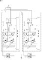
図1は、自立運転する2台のインバータ1,2を、交流電路5に対して並列に接続した、並列インバータシステム100の一例を示す接続図である。なお、各インバータ1,2は、商用電力系統と系統連系して運転することもできるが、本開示では、自立運転時の状態についてのみ示している。2台のインバータとしたのは「複数」の最小限構成例であり、3台以上であってもよい。 《Parallel inverter system》
FIG. 1 is a connection diagram showing an example of a
次に、制御部1Aの機能(制御部2Aも同様であり、以下、単に「制御部」と言う。)について説明する。
図2は、制御部における電圧制御に関する制御ブロック図である。なお、この図は、説明の簡素化のため、電流制御ループを含まない最もシンプルな例としている。また、図3は、図2の制御ブロック図を、フローチャートとして表現した図である。 <<Functions of control unit>>
Next, the function of the
FIG. 2 is a control block diagram regarding voltage control in the control unit. Note that this diagram shows the simplest example that does not include a current control loop for the sake of simplification of explanation. 3 is a diagram expressing the control block diagram of FIG. 2 as a flow chart.
まず、図3において、制御部は、位相差検出値Δθを求める(ステップS1)。
図2では、位相差検出器B1に、交流電圧vaと内部位相(前回値)θとが入力され、位相差検出値Δθが得られる。 2 and 3 will be described below in association with each other.
First, in FIG. 3, the control unit obtains the phase difference detection value Δθ (step S1).
In FIG. 2, the AC voltage va and the internal phase (previous value) θ are input to the phase difference detector B1 to obtain the phase difference detection value Δθ.
図2では、位相差検出値Δθが、第1比例積分器B2を経て、周波数補正値Δf1となる。 Next, in FIG. 3, the control unit obtains the first frequency correction value Δf1 (step S2).
In FIG. 2, the phase difference detection value Δθ becomes the frequency correction value Δf1 through the first proportional integrator B2.
図2では、加算器B5において、周波数基準値foと、周波数検出値fの前回値とが比較され、その差が、第2比例積分器B6を経て、周波数補正値Δf2となる。 Next, in FIG. 3, the control unit obtains a second frequency correction value Δf2 (step S3).
In FIG. 2, the adder B5 compares the frequency reference value fo with the previous value of the detected frequency value f, and the difference between them becomes the frequency correction value Δf2 via the second proportional integrator B6.
図2では、周波数補正値Δf1と、周波数補正値Δf2と、周波数基準値foとが相互に加算器B3により加算され、新しい周波数検出値fが得られる。最初に、新しい周波数検出値fを決める際は、前回値の周波数検出値fが用いられる。 Next, in FIG. 3, the control unit obtains a frequency detection value f (step S4).
In FIG. 2, the frequency correction value Δf1, the frequency correction value Δf2, and the frequency reference value fo are added together by the adder B3 to obtain a new frequency detection value f. First, when determining a new frequency detection value f, the previous frequency detection value f is used.
図2では、周波数検出値fが積分器B4を経て内部位相θとなる。内部位相θは、位相同期ループLの出力であり、また、この位相同期ループLの中に、ループ内ループとして、周波数フィードバックループFが組み込まれていることになる。 Next, in FIG. 3, the controller obtains the internal phase θ (step S5).
In FIG. 2, the frequency detection value f becomes the internal phase θ through the integrator B4. The internal phase .theta. is the output of the phase-locked loop L, and the phase-locked loop L incorporates the frequency feedback loop F as a loop within the loop.
図2では、内部位相θと、電圧振幅基準値E0とに基づいて、電圧指令部B7が電圧指令値va*を出力する。 Next, in FIG. 3, the controller obtains the voltage command value va * (step S6).
In FIG. 2, the voltage command unit B7 outputs the voltage command value va * based on the internal phase θ and the voltage amplitude reference value E0.
図2では、電圧指令値va*と交流電圧vaとが加算器B8により比較され、比例器B9により比例処理を施されて電圧補正値Δvaとなる。なお、電圧補正値Δvaを求める演算には、交流電流iaを用いることもできる。 Next, in FIG. 3, the control unit obtains the voltage correction value Δva (step S7).
In FIG. 2, the voltage command value va * and the AC voltage va are compared by an adder B8 and subjected to proportional processing by a proportional device B9 to obtain a voltage correction value .DELTA.va. It should be noted that the AC current ia can also be used for the calculation for obtaining the voltage correction value Δva.
図2では、電圧指令値va*と電圧補正値Δvaとに基づいてPWM信号生成部B10により、パルス幅変調されたインバータ制御信号が生成され、これに基づいてインバータのゲート駆動信号が得られる。PWM信号生成部B10には、直流電圧viも与えられている。 Then, in FIG. 3, the control unit obtains a control signal for the inverter (step S8).
In FIG. 2, the PWM signal generator B10 generates a pulse width modulated inverter control signal based on the voltage command value va * and the voltage correction value Δva, and based on this, the inverter gate drive signal is obtained. A DC voltage vi is also applied to the PWM signal generator B10.
図2において、位相差検出器B1、第1比例積分器B2、加算器B3、及び、積分器B4は、位相同期ループLを形成している。
また、加算器B3、加算器B5、及び、第2比例積分器B6は、周波数フィードバックループFを形成している。自立運転ではなく、系統連系運転を行う場合のインバータは、このような周波数フィードバックループFを使用しなくてもよい。 The processing shown in the flow chart of FIG. 3 is repeatedly executed while the
In FIG. 2, the phase difference detector B1, the first proportional integrator B2, the adder B3 and the integrator B4 form a phase locked loop L. In FIG.
The adder B3, the adder B5, and the second proportional integrator B6 form a frequency feedback loop F. Such a frequency feedback loop F does not need to be used for an inverter that performs grid-connected operation instead of isolated operation.
まず、上記のような周波数フィードバックループを使用しない制御の参考例から、シミュレーションにより検証する。 "inspection"
First, we will verify by simulation from the reference example of the control that does not use the frequency feedback loop as described above.
図4は、系統連系運転を行う場合と同様の制御により、第1,第2の2台のインバータを自立出力で並列運転した場合の、シミュレーション結果である。(a),(b),(c),(d)における横軸は共通であり、時間を表している(0~2秒)。縦軸の数値は、電圧、電流又は周波数を表している。この制御では、第1のインバータを先に運転して、1秒後に第2のインバータの運転を開始している。 (Reference example 1)
FIG. 4 shows the simulation results when the first and second inverters are operated in parallel with the self-sustained output under the same control as in the grid-connected operation. The horizontal axis in (a), (b), (c) and (d) is common and represents time (0 to 2 seconds). The numbers on the vertical axis represent voltage, current or frequency. In this control, the first inverter is operated first, and the operation of the second inverter is started after one second.
(b)は、dq変換後の2相の電圧vd(上)、vq(下)の波形図である。
(c)は、位相同期ループの出力周波数である。
(d)は、第1のインバータ及び第2のインバータの出力電流である。0~約1.1秒までは、振幅の大きい方が第1のインバータ、振幅の小さい方が第2のインバータである。約1.1秒~約1.5秒では、両者が互いに重なっている。 (a) is a waveform diagram in which an AC voltage va and an AC current output by a first inverter are superimposed and displayed. The AC voltage va has a larger amplitude, and the AC current has a smaller amplitude.
(b) is a waveform diagram of two-phase voltages vd (upper) and vq (lower) after dq conversion.
(c) is the output frequency of the phase locked loop.
(d) is the output current of the first inverter and the second inverter. From 0 to about 1.1 seconds, the larger amplitude is the first inverter and the smaller amplitude is the second inverter. From about 1.1 seconds to about 1.5 seconds, both overlap each other.
図5は、周波数を60Hzに固定した基準電圧信号を用いて、第1,第2の2台のインバータを自立出力で並列運転した場合の、シミュレーション結果である。(a),(b),(c),(d)における横軸は共通であり、時間を表している(0~10秒)。縦軸の数値は、電圧、電流又は周波数を表している。右端には、10秒直前の横軸(時間軸)を拡大し、かつ、(c)及び(d)については縦軸も拡大した図を示している。 (Reference example 2)
FIG. 5 shows the simulation results when the first and second inverters are operated in parallel with the independent output using a reference voltage signal whose frequency is fixed at 60 Hz. The horizontal axis in (a), (b), (c) and (d) is common and represents time (0 to 10 seconds). The numbers on the vertical axis represent voltage, current or frequency. At the right end, the horizontal axis (time axis) just before 10 seconds is enlarged, and the vertical axis is also enlarged for (c) and (d).
(b)は、dq変換後の2相の電圧vd(上)、vq(下)の波形図である。
(c)は、位相同期ループの出力周波数である。
(d)は、第1のインバータ及び第2のインバータの出力電流である。第1のインバータより1秒遅れて第2のインバータが運転開始している。 (a) is a waveform diagram in which an AC voltage va and an AC current output by a first inverter are superimposed and displayed. The AC voltage va has a larger amplitude, and the AC current oscillates near zero.
(b) is a waveform diagram of two-phase voltages vd (upper) and vq (lower) after dq conversion.
(c) is the output frequency of the phase locked loop.
(d) is the output current of the first inverter and the second inverter. The second inverter starts operating one second later than the first inverter.
図6は、図2の制御ブロック図に基づく制御を行った場合の、シミュレーション結果である。(a),(b),(c),(d)における横軸は共通であり、時間を表している(0~10秒)。縦軸の数値は、電圧、電流又は周波数を表している。右端には、10秒直前の横軸(時間軸)を拡大し、かつ、(c)及び(d)については縦軸も拡大した図を示している。周波数フィードバックループFにおける第2比例積分器B6の比例ゲインを0.2、積分時定数を0.01秒とした。 (Control based on the control block diagram of FIG. 2)
FIG. 6 shows simulation results when control is performed based on the control block diagram of FIG. The horizontal axis in (a), (b), (c) and (d) is common and represents time (0 to 10 seconds). The numbers on the vertical axis represent voltage, current or frequency. At the right end, the horizontal axis (time axis) just before 10 seconds is enlarged, and the vertical axis is also enlarged for (c) and (d). The proportional gain of the second proportional integrator B6 in the frequency feedback loop F was set to 0.2, and the integration time constant was set to 0.01 seconds.
(b)は、dq変換後の2相の電圧vd(上)、vq(下)の波形図である。
(c)は、位相同期ループの出力周波数である。
(d)は、第1のインバータ及び第2のインバータの出力電流である。第1のインバータより1秒遅れて第2のインバータが運転開始している。 (a) is a waveform diagram in which an AC voltage va and an AC current output by a first inverter are superimposed and displayed. The AC voltage va has a larger amplitude, and the AC current oscillates near zero.
(b) is a waveform diagram of two-phase voltages vd (upper) and vq (lower) after dq conversion.
(c) is the output frequency of the phase locked loop.
(d) is the output current of the first inverter and the second inverter. The second inverter starts operating one second later than the first inverter.
図8の(a)は、図2に示す周波数フィードバック付きの位相同期ループを有するインバータの、並列運転を行った場合において、インバータ(電力変換部)の出力電流Iと、内部位相差φとの関係の一例を示すグラフである。位相差φは出力電流Iと比例的な関係にあり、出力電流Iが増大すれば、位相差φも増大する。これは、同期発電機の出力電流と内部位相角との関係と同様である。 《Parallel operation with a generator》
FIG. 8(a) shows the relationship between the output current I of the inverter (power converter) and the internal phase difference φ when the inverters having the phase-locked loop with frequency feedback shown in FIG. 2 are operated in parallel. It is a graph which shows an example of relationship. The phase difference φ is in a proportional relationship with the output current I, and as the output current I increases, the phase difference φ also increases. This is similar to the relationship between the output current of a synchronous generator and the internal phase angle.
φ≒(jxsI)/E
すなわち、位相同期ループに周波数フィードバック処理を付加したインバータは、一種の仮想同期発電機(VSG:Vertual Synchronous Generator)として動作する。従って、当該インバータは、同期発電機との並列運転も可能である。 (b) of FIG. 8 is a vector diagram showing the relationship between the equivalent induced electromotive force E, the phase difference φ, and the AC voltage V. FIG. Here, if the inverter is considered as a synchronous generator with a synchronous reactance of x s , and the phase difference φ is sin φ≈φ, the following relationship is obtained.
φ≈( jxsI )/E
That is, an inverter with frequency feedback processing added to a phase-locked loop operates as a kind of virtual synchronous generator (VSG: Virtual Synchronous Generator). Therefore, the inverter can also be operated in parallel with the synchronous generator.
(b)は、dq変換後の2相の電圧vd(上)、vq(下)の波形図である。
(c)は、位相同期ループの出力周波数である。
(d)は、第1のインバータ及び第2のインバータの出力電流である。時刻10秒で発電機を解列している。 (a) of FIG. 7 is a waveform diagram in which the AC voltage va and the AC current output by the first inverter are superimposed and displayed. The AC voltage va has a larger amplitude, and the AC current oscillates near zero.
(b) is a waveform diagram of two-phase voltages vd (upper) and vq (lower) after dq conversion.
(c) is the output frequency of the phase locked loop.
(d) is the output current of the first inverter and the second inverter. The generator is disconnected at 10 seconds.
v*=E*cos2πf*t
とすると、無効電力の増大に応じて電圧振幅目標値E*が低下し、また、有効電力の増大に応じて周波数目標値f*が低下する垂下特性を付与することが考えられる。 In order to control the ratio of the current borne by the two inverters, it is sufficient to change the control target value according to the output of the inverter. If the voltage phase is advanced, the active power increases, and if the voltage amplitude is increased, the reactive power increases.
v * =E * cos2πf * t
Then, it is conceivable to provide a drooping characteristic in which the voltage amplitude target value E * decreases as the reactive power increases, and the frequency target value f * decreases as the active power increases.
以上の開示は、一般化して以下のように表現することができる。
図1に示した第1のインバータ(1)及び第2のインバータ(2)の各々における制御部は、交流電圧(Va)に基づいて実行する位相同期ループ(L)において周波数検出値を算出する演算に、当該周波数検出値の前回値と周波数基準値との比較結果に比例積分を施して得た周波数補正値(Δf2)を加える周波数フィードバック処理(周波数フィードバックループ(F))を付加している。
このようなインバータは、自立出力の周波数が目標値に漸近して収束する。従って、かかるインバータを複数台並列に接続した場合、または、他の交流電源と並列接続した場合に、安定した並列運転を行うことができる。 "summary"
The above disclosure can be generalized and expressed as follows.
The control unit in each of the first inverter (1) and the second inverter (2) shown in FIG. 1 calculates the frequency detection value in the phase locked loop (L) executed based on the AC voltage (Va) A frequency feedback process (frequency feedback loop (F)) is added to the calculation to add a frequency correction value (Δf2) obtained by performing proportional integration on the comparison result between the previous value of the frequency detection value and the frequency reference value. .
In such an inverter, the frequency of the self-sustained output asymptotically approaches the target value and converges. Therefore, when a plurality of such inverters are connected in parallel, or when they are connected in parallel with another AC power supply, stable parallel operation can be performed.
上記の第2演算を行うことにより、自立出力の周波数が収束しない状態に陥るのを抑制することができる。 More specifically, assuming that the frequency correction value (Δf2) is the second frequency correction value, the control unit adjusts the voltage phase based on the detection output of the voltage sensor (19, 29) and the phase-locked loop (L). A first calculation for obtaining a first frequency correction value (Δf1) based on the deviation from the internal phase, and a frequency reference value (fo) with the first frequency correction value (Δf1) and the second frequency correction value ( Δf2) to obtain a new frequency detection value (f); and a third operation that generates a control signal that controls the output.
By performing the second calculation, it is possible to prevent the frequency of the self-sustained output from converging.
この場合、比例積分演算ではなく比例演算を行うことにより、他の交流電源との間で、交流電圧として検出した値に差があっても、横流を抑制することができる。 Further, the third calculation includes obtaining the voltage command value (va * ) based on the new frequency detection value (f), and proportional calculation to the deviation between the voltage command value (va * ) and the AC voltage. to determine the voltage correction value (Δva).
In this case, by performing the proportional calculation instead of the proportional integral calculation, even if there is a difference in the value detected as the AC voltage between the other AC power supplies, the cross current can be suppressed.
図1のインバータ1,2は、自立出力のインバータとして説明したが、直流電圧源が蓄電池に基づく場合は、インバータ1,2(電力変換部1B,2B)は、交流電力から直流電力への変換を行うようにしてもよい。例えば、交流電路5に、太陽光発電を電源とする系統連系型のインバータのように、交流電路5の電圧に同期する電流を出力する交流電源(電流源)が接続された場合を考える。この場合、制御部1A,2Aは、交流電源の交流電力を直流電力に変換して電力変換部1B,2Bの直流側に接続される蓄電池を充電するよう制御する。負荷6での消費電力の余剰電力を、インバータ1,2が順変換(交流→直流)して直流電圧源3,4に含まれる蓄電池を充電することができる。なお。この場合は、インバータの位相同期ループにおける内部位相は、交流電圧の位相より遅れる。 《Supplementary information on forward conversion (charging)》
Although the
なお、図1のフルブリッジ回路10,20は、2レグの単相インバータ回路であるが、3レグの三相インバータ回路であっても、同様に、図2、図3の処理を適用することができる。 "others"
Although the
なお、今回開示された実施の形態はすべての点で例示であって制限的なものではないと考えられるべきである。本発明の範囲は請求の範囲によって示され、請求の範囲と均等の意味及び範囲内での全ての変更が含まれることが意図される。 《Supplement》
It should be noted that the embodiments disclosed this time should be considered as examples in all respects and not restrictive. The scope of the present invention is indicated by the claims, and is intended to include all changes within the meaning and range of equivalents to the claims.
1A 制御部
1B 電力変換部
2 第2のインバータ
2A 制御部
2B 電力変換部
3,4 直流電圧源
5 交流電路
6 負荷
10 フルブリッジ回路
11,12,13,14 スイッチング素子
11d,12d,13d,14d ダイオード
15 交流リアクトル
16交流側コンデンサ
17 電圧センサ
18 電流センサ
19 電圧センサ
20 フルブリッジ回路
21,22,23,24 スイッチング素子
21d,22d,23d,24d ダイオード
25 交流リアクトル
26交流側コンデンサ
27 電圧センサ
28 電流センサ
29 電圧センサ
100 並列インバータシステム
B1 位相差検出器
B2 第1比例積分器
B3 加算器
B4 積分器
B5 加算器
B6 第2比例積分器
B7 電圧指令部
B8 加算器
B9 比例器
B10 PWM信号生成部
F 周波数フィードバックループ
L 位相同期ループ 1
Claims (7)
- 交流電源が接続された交流電路に並列に接続され自立出力を提供するインバータであって、
直流電力を交流電力に変換して前記交流電路に電力を供給する電力変換部と、
前記交流電路の交流電圧を検出する電圧センサと、
前記電力変換部を制御する制御部と、を備え、
前記制御部は、前記交流電圧に基づいて実行する位相同期ループにおいて周波数検出値を算出する演算に、当該周波数検出値の前回値と周波数基準値との比較結果に比例積分を施して得た周波数補正値を加える周波数フィードバック処理を付加する、インバータ。 An inverter that is connected in parallel to an AC electric circuit to which an AC power supply is connected and provides an independent output,
a power conversion unit that converts DC power into AC power and supplies power to the AC electric line;
a voltage sensor that detects an AC voltage of the AC electric circuit;
A control unit that controls the power conversion unit,
The control unit, in the calculation for calculating the frequency detection value in the phase-locked loop executed based on the AC voltage, the frequency obtained by performing proportional integration on the result of comparison between the previous value of the frequency detection value and the frequency reference value. An inverter that adds a frequency feedback process that adds a correction value. - 前記周波数補正値を第2の周波数補正値とすると、前記制御部は、
前記電圧センサの検出出力に基づく電圧位相と前記位相同期ループ内の内部位相との偏差に基づいて、第1の周波数補正値を求める第1演算と、
前記周波数基準値に、前記第1の周波数補正値及び前記第2の周波数補正値を加算して新たな周波数検出値を求める第2演算と、
前記新たな周波数検出値に基づいて前記電力変換部の出力を制御する制御信号を生成する第3演算と、
を実行する請求項1に記載のインバータ。 Assuming that the frequency correction value is a second frequency correction value, the control unit
a first calculation for obtaining a first frequency correction value based on a deviation between a voltage phase based on the detection output of the voltage sensor and an internal phase within the phase-locked loop;
a second calculation for obtaining a new frequency detection value by adding the first frequency correction value and the second frequency correction value to the frequency reference value;
a third calculation for generating a control signal for controlling the output of the power conversion unit based on the new frequency detection value;
2. The inverter of claim 1, which performs - 前記第3演算には、
前記新たな周波数検出値に基づいて電圧指令値を求めること、及び、
前記電圧指令値と、前記交流電圧との偏差に、比例演算を施して電圧補正値を求めること、
が含まれる請求項2に記載のインバータ。 In the third calculation,
obtaining a voltage command value based on the new frequency detection value; and
obtaining a voltage correction value by performing a proportional operation on the deviation between the voltage command value and the AC voltage;
3. The inverter of claim 2, comprising: - 前記内部位相は、前記電力変換部の出力電流に応じて変化する前記交流電圧の位相、に対して位相差を有する請求項2又は請求項3に記載のインバータ。 The inverter according to claim 2 or 3, wherein the internal phase has a phase difference with respect to the phase of the AC voltage that changes according to the output current of the power conversion unit.
- 前記電力変換部は、交流電力から直流電力への変換も可能であり、
前記制御部は、前記交流電源の交流電力を直流電力に変換して前記電力変換部の直流側に接続される直流電圧源を充電するよう、前記電力変換部を制御する請求項1から請求項4のいずれか1項に記載のインバータ。 The power conversion unit is also capable of converting AC power to DC power,
The control unit controls the power conversion unit such that the AC power of the AC power source is converted into DC power and a DC voltage source connected to the DC side of the power conversion unit is charged. 5. The inverter according to any one of 4. - 交流電路に自立出力を提供する第1インバータと、
前記第1インバータと並列に前記交流電路に接続され、前記交流電路に自立出力を提供する第2インバータと、を備えた並列インバータシステムであって、
前記第1インバータ及び前記第2インバータの各々は、
直流電力を交流電力に変換して前記交流電路に電力を供給する電力変換部と、
前記交流電路の交流電圧を検出する電圧センサと、
前記電力変換部を制御する制御部と、を備え、
前記制御部は、前記交流電圧に基づいて実行する位相同期ループにおいて周波数検出値を算出する演算に、当該周波数検出値の前回値と周波数基準値との比較結果に比例積分を施して得た周波数補正値を加える周波数フィードバック処理を付加する、並列インバータシステム。 a first inverter that provides a self-sustaining output to the AC circuit;
A parallel inverter system comprising: a second inverter connected in parallel with the first inverter to the AC electric line and providing a self-sustaining output to the AC electric line,
each of the first inverter and the second inverter,
a power conversion unit that converts DC power into AC power and supplies power to the AC electric line;
a voltage sensor that detects an AC voltage of the AC electric circuit;
A control unit that controls the power conversion unit,
The control unit, in the calculation for calculating the frequency detection value in the phase-locked loop executed based on the AC voltage, the frequency obtained by performing proportional integration on the result of comparison between the previous value of the frequency detection value and the frequency reference value. A parallel inverter system with added frequency feedback processing that adds a correction value. - 交流電源が接続された交流電路に並列に接続され自立出力を提供するインバータの制御方法であって、
電力変換部により、直流電力を交流電力に変換して前記交流電路に電力を供給し、
前記電力変換部を制御する制御部は、前記交流電路の交流電圧に基づいて実行する位相同期ループにおいて周波数検出値を算出する演算に、当該周波数検出値の前回値と周波数基準値との比較結果に比例積分を施して得た周波数補正値を加える周波数フィードバック処理を付加する、
インバータの制御方法。
A control method for an inverter that is connected in parallel to an AC electric circuit to which an AC power supply is connected and provides an independent output,
A power conversion unit converts DC power into AC power and supplies power to the AC electric circuit,
A control unit that controls the power conversion unit includes a comparison result between a previous value of the frequency detection value and a frequency reference value in an operation for calculating a frequency detection value in a phase-locked loop that is executed based on the AC voltage of the AC electric circuit. Add a frequency feedback process that adds a frequency correction value obtained by performing proportional integration on
Inverter control method.
Priority Applications (1)
| Application Number | Priority Date | Filing Date | Title |
|---|---|---|---|
| JP2023503375A JPWO2022185614A1 (en) | 2021-03-03 | 2021-11-02 |
Applications Claiming Priority (2)
| Application Number | Priority Date | Filing Date | Title |
|---|---|---|---|
| JP2021-033734 | 2021-03-03 | ||
| JP2021033734 | 2021-03-03 |
Publications (1)
| Publication Number | Publication Date |
|---|---|
| WO2022185614A1 true WO2022185614A1 (en) | 2022-09-09 |
Family
ID=83154244
Family Applications (1)
| Application Number | Title | Priority Date | Filing Date |
|---|---|---|---|
| PCT/JP2021/040360 WO2022185614A1 (en) | 2021-03-03 | 2021-11-02 | Inverter, parallel inverter system, and method for controlling inverter |
Country Status (2)
| Country | Link |
|---|---|
| JP (1) | JPWO2022185614A1 (en) |
| WO (1) | WO2022185614A1 (en) |
Citations (3)
| Publication number | Priority date | Publication date | Assignee | Title |
|---|---|---|---|---|
| JP2010161901A (en) * | 2009-01-09 | 2010-07-22 | Daihen Corp | Inverter control circuit and grid-connected inverter system with this inverter control circuit |
| JP2015100224A (en) * | 2013-11-20 | 2015-05-28 | 株式会社ダイヘン | Control circuit for controlling inverter circuit, inverter device including the control circuit, power system including the inverter device, and control method |
| JP2017225214A (en) * | 2016-06-13 | 2017-12-21 | 新電元工業株式会社 | Parallel operation control method and parallel operation control apparatus for three-phase inverter |
-
2021
- 2021-11-02 JP JP2023503375A patent/JPWO2022185614A1/ja active Pending
- 2021-11-02 WO PCT/JP2021/040360 patent/WO2022185614A1/en active Application Filing
Patent Citations (3)
| Publication number | Priority date | Publication date | Assignee | Title |
|---|---|---|---|---|
| JP2010161901A (en) * | 2009-01-09 | 2010-07-22 | Daihen Corp | Inverter control circuit and grid-connected inverter system with this inverter control circuit |
| JP2015100224A (en) * | 2013-11-20 | 2015-05-28 | 株式会社ダイヘン | Control circuit for controlling inverter circuit, inverter device including the control circuit, power system including the inverter device, and control method |
| JP2017225214A (en) * | 2016-06-13 | 2017-12-21 | 新電元工業株式会社 | Parallel operation control method and parallel operation control apparatus for three-phase inverter |
Also Published As
| Publication number | Publication date |
|---|---|
| JPWO2022185614A1 (en) | 2022-09-09 |
Similar Documents
| Publication | Publication Date | Title |
|---|---|---|
| US8848406B2 (en) | Single-phase voltage type AC/DC converter, three-phase voltage type AC/DC converter, and stabilization control method | |
| US9166500B2 (en) | Power decoupling controller and method for power conversion system | |
| US8848400B2 (en) | System and method for reactive power regulation | |
| US8009450B2 (en) | Method and apparatus for phase current balance in active converter with unbalanced AC line voltage source | |
| JP5300028B2 (en) | Single-phase voltage type AC / DC converter and system interconnection system | |
| US10411478B2 (en) | Grid connection power conversion device and disconnection/welding detection method therefor | |
| US20130181654A1 (en) | Motor drive system employing an active rectifier | |
| JP4664836B2 (en) | Three-phase voltage type AC / DC converter | |
| JP2009219263A (en) | Single-phase voltage type ac-dc converter | |
| JP2575500B2 (en) | Three-phase converter | |
| JP2012085482A (en) | Distributed power supply system | |
| JP6744477B2 (en) | Uninterruptible power supply and test method for uninterruptible power supply | |
| JP2011055591A (en) | Inverter control circuit and grid-connected inverter system with the same | |
| WO2022185614A1 (en) | Inverter, parallel inverter system, and method for controlling inverter | |
| Gonzatti et al. | Implementation of a grid-forming converter based on modified synchronous reference frame | |
| Zhu et al. | Grid synchronization control without AC voltage sensors | |
| JP4052154B2 (en) | Distributed power supply output stabilization device and control method thereof. | |
| US20240136947A1 (en) | Inverter, parallel inverter system, and method of controlling inverter | |
| JP7136368B2 (en) | power converter | |
| WO2014050935A1 (en) | Single-phase voltage type ac-dc conversion device | |
| Liu et al. | Distributed generation interface using indirect matrix converter in boost mode with controllable grid side reactive power | |
| US7233081B2 (en) | Power-supply device | |
| WO2014050759A1 (en) | Single-phase voltage type ac-dc converter | |
| JP5616412B2 (en) | Single-phase voltage type AC / DC converter | |
| WO2014050758A1 (en) | Single-phase voltage type ac-dc conversion device |
Legal Events
| Date | Code | Title | Description |
|---|---|---|---|
| 121 | Ep: the epo has been informed by wipo that ep was designated in this application |
Ref document number: 21929174 Country of ref document: EP Kind code of ref document: A1 |
|
| WWE | Wipo information: entry into national phase |
Ref document number: 2023503375 Country of ref document: JP |
|
| WWE | Wipo information: entry into national phase |
Ref document number: 18278410 Country of ref document: US |
|
| NENP | Non-entry into the national phase |
Ref country code: DE |
|
| 122 | Ep: pct application non-entry in european phase |
Ref document number: 21929174 Country of ref document: EP Kind code of ref document: A1 |