US5461297A - Series-parallel switchable capacitor charging system - Google Patents
Series-parallel switchable capacitor charging system Download PDFInfo
- Publication number
- US5461297A US5461297A US08/065,994 US6599493A US5461297A US 5461297 A US5461297 A US 5461297A US 6599493 A US6599493 A US 6599493A US 5461297 A US5461297 A US 5461297A
- Authority
- US
- United States
- Prior art keywords
- capacitor
- charging
- rectified current
- additional
- positive
- Prior art date
- Legal status (The legal status is an assumption and is not a legal conclusion. Google has not performed a legal analysis and makes no representation as to the accuracy of the status listed.)
- Expired - Lifetime
Links
Images


Classifications
-
- H—ELECTRICITY
- H02—GENERATION; CONVERSION OR DISTRIBUTION OF ELECTRIC POWER
- H02M—APPARATUS FOR CONVERSION BETWEEN AC AND AC, BETWEEN AC AND DC, OR BETWEEN DC AND DC, AND FOR USE WITH MAINS OR SIMILAR POWER SUPPLY SYSTEMS; CONVERSION OF DC OR AC INPUT POWER INTO SURGE OUTPUT POWER; CONTROL OR REGULATION THEREOF
- H02M3/00—Conversion of dc power input into dc power output
- H02M3/22—Conversion of dc power input into dc power output with intermediate conversion into ac
- H02M3/24—Conversion of dc power input into dc power output with intermediate conversion into ac by static converters
- H02M3/28—Conversion of dc power input into dc power output with intermediate conversion into ac by static converters using discharge tubes with control electrode or semiconductor devices with control electrode to produce the intermediate ac
- H02M3/325—Conversion of dc power input into dc power output with intermediate conversion into ac by static converters using discharge tubes with control electrode or semiconductor devices with control electrode to produce the intermediate ac using devices of a triode or a transistor type requiring continuous application of a control signal
- H02M3/335—Conversion of dc power input into dc power output with intermediate conversion into ac by static converters using discharge tubes with control electrode or semiconductor devices with control electrode to produce the intermediate ac using devices of a triode or a transistor type requiring continuous application of a control signal using semiconductor devices only
- H02M3/33561—Conversion of dc power input into dc power output with intermediate conversion into ac by static converters using discharge tubes with control electrode or semiconductor devices with control electrode to produce the intermediate ac using devices of a triode or a transistor type requiring continuous application of a control signal using semiconductor devices only having more than one ouput with independent control
-
- H—ELECTRICITY
- H02—GENERATION; CONVERSION OR DISTRIBUTION OF ELECTRIC POWER
- H02M—APPARATUS FOR CONVERSION BETWEEN AC AND AC, BETWEEN AC AND DC, OR BETWEEN DC AND DC, AND FOR USE WITH MAINS OR SIMILAR POWER SUPPLY SYSTEMS; CONVERSION OF DC OR AC INPUT POWER INTO SURGE OUTPUT POWER; CONTROL OR REGULATION THEREOF
- H02M3/00—Conversion of dc power input into dc power output
- H02M3/22—Conversion of dc power input into dc power output with intermediate conversion into ac
- H02M3/24—Conversion of dc power input into dc power output with intermediate conversion into ac by static converters
- H02M3/28—Conversion of dc power input into dc power output with intermediate conversion into ac by static converters using discharge tubes with control electrode or semiconductor devices with control electrode to produce the intermediate ac
-
- H—ELECTRICITY
- H02—GENERATION; CONVERSION OR DISTRIBUTION OF ELECTRIC POWER
- H02M—APPARATUS FOR CONVERSION BETWEEN AC AND AC, BETWEEN AC AND DC, OR BETWEEN DC AND DC, AND FOR USE WITH MAINS OR SIMILAR POWER SUPPLY SYSTEMS; CONVERSION OF DC OR AC INPUT POWER INTO SURGE OUTPUT POWER; CONTROL OR REGULATION THEREOF
- H02M7/00—Conversion of ac power input into dc power output; Conversion of dc power input into ac power output
- H02M7/02—Conversion of ac power input into dc power output without possibility of reversal
- H02M7/04—Conversion of ac power input into dc power output without possibility of reversal by static converters
- H02M7/06—Conversion of ac power input into dc power output without possibility of reversal by static converters using discharge tubes without control electrode or semiconductor devices without control electrode
- H02M7/10—Conversion of ac power input into dc power output without possibility of reversal by static converters using discharge tubes without control electrode or semiconductor devices without control electrode arranged for operation in series, e.g. for multiplication of voltage
Definitions
- the invention relates to power supplies, more particularly to power supplies for charging a capacitor, such as employed in a pulsed laser system.
- Certain high voltage power supply applications require that a capacitor be charged to a high voltage, and subsequently rapidly discharged through a device.
- Examples include xenon flash-tubes (such as are commonly used in lab strobes, photo-flash units, etc.), pulsed lasers (medical, industrial, military, and scientific applications), and other types of discharge devices.
- Discharges from solid state pulsed lasers for example are often accomplished by firing a flash tube surrounding a solid state laser rod.
- Capacitors are often used for such applications because high voltage capacitors are relatively easy to obtain, and because capacitors can be discharged extremely rapidly (by drawing current from the capacitor). (Other applications which discharge the capacitor more slowly are also possible.)
- the frequency with which the capacitor may be discharged, i.e., the discharge rate e.g., pulse rate on a strobe light or laser, frame rate on a camera photo-flash unit
- the discharge rate is limited, at least in part, by the rate at which the capacitor can be charged (made ready for discharge) by an associated charging power supply.
- the voltage across a capacitor increases as the product of the capacitance value of the capacitor and the integral with respect to time of the current through the capacitor. Consequently, the greater the capacitance, the longer it takes to charge the capacitor through a given voltage increase across the capacitor for a given charging current. Conversely, the greater the charging current, the more rapidly a capacitor can be charged.
- the charge (in coulombs) on a capacitor is equal to the product of the voltage across the capacitor and the value of the capacitor.
- the amount of electrical energy stored in a capacitor is equal to one half the product of the capacitance value and the square of the voltage across the capacitor.
- High output devices e.g., high output pulsed lasers
- Many applications e.g., medical surgical lasers
- Rapid pulsed operation requires rapid charging of the capacitor, requiring correspondingly high current from the capacitor-charging power supply.
- COFFEY A capacitor charging system which addresses the problems of surge current and size, in part, is described in U.S. Pat. No. 3,654,537, (hereinafter "COFFEY"), incorporated by reference herein.
- COFFEY describes a technique whereby an energy storage capacitor is charged in a series of successive steps, each of a higher voltage level than the preceding step.
- power from each of a series of unequal secondary windings of a transformer is rectified and selectively switched into a stacked series arrangement.
- the capacitor can be charged in a number of controlled voltage steps effectively limiting surge currents without requiring large inductors. Current into the capacitor is maintained at a relatively constant level over the charging cycle. Further, charging efficiency is considerably improved.
- COFFEY does little to increase the output current of the supply into the capacitor.
- Another disadvantage of COFFEY is that at any given time, a number of the windings of the transformer may not be in use, implying a rather poor size to charging-rate ratio for the transformer. Since the rate of energy transfer into a capacitor for a given current is proportional to the voltage across the capacitor, the COFFEY technique transfers the most energy in the last part of the charging cycle (which makes intuitive sense, since the last part of the cycle is when more of the secondary winding are switched in). As a result, the load seen at the primary of the transformer increases throughout the charging cycle.
- TAKENAKA Another approach is shown in Japanese Patent No. 1-286800 (hereinafter TAKENAKA).
- TAKENAKA a pair of windings of a generator block are first connected in parallel, and then in series. The output is rectified and used to charge a capacitor. When the capacitor is in its fully discharged state, the parallel winding combination is used, providing roughly double the current which could be supplied by a single winding alone. When the voltage across the capacitor reaches a critical point (related to the single winding voltage for the transformer) the two windings are switched into a series configuration, halving the current carrying capacity of the combined windings, but doubling the voltage. The rectified voltage from the series combination charges the capacitor for the remainder of the charging cycle.
- the TAKENAKA approach has the advantages (e.g., over COFFEY) of maintaining both windings "active" at all times, and providing a more constant and optimal rate of energy transfer to the capacitor, thereby improving the size to charging-rate ratio for the transformer and speeding up the charging cycle. Nevertheless, the TAKENAKA approach suffers from significant disadvantages. In order to switch the (two) windings from a series to a parallel configuration, three FET (field effect transistor switches) are required. The controls for these switches can be rather cumbersome and expensive. Further, since the rectifier must handle both the series and parallel coil winding combinations, it must be capable of handling both high current and high voltage.
- a series/parallel switchable charging system for an energy storage capacitor is employed in conjunction with a transformer having two or more secondary windings.
- Each of the secondary windings is separately rectified, providing a positive output and a negative output associated with each winding.
- the positive output associated with a first of these two secondary windings is designated a positive charging output and is connected to a positive terminal of a capacitor to be charged.
- the negative output associated with the other, or second, secondary winding is designated a negative charging output and is connected to a negative terminal of the capacitor to be charged.
- Two diodes and a switch provide means for switching the two secondary windings into a parallel conducting configuration when the switch is open or, alternatively, into a series conducting configuration when the switch is closed.
- a first diode is anode-connected to the positive output associated with the second secondary winding and cathode-connected to the positive output associated with the first secondary winding.
- the other, or second, diode is anode connected to the negative output associated with the second secondary winding and cathode-connected to the negative output associated with the first secondary winding.
- the switch is connected between the negative output associated with the first secondary winding and the positive output associated with the second secondary winding.
- both diodes When the switch is closed, both diodes are reverse biased, and the positive and negative outputs associated with the two secondary windings are effectively connected, via the switch, in a series configuration.
- the series connection is broken and the diodes conduct (forward bias), effectively connecting the positive and negative outputs associated with the two secondary windings into a parallel configuration.
- a voltage monitor controls closure of the switch according to a monitored voltage. If the voltage is higher than a preset threshold voltage, then the switch is closed. As stated hereinabove, the rate of energy transfer into a capacitor is proportional, at a given level of charging current, to the voltage across the capacitor. Assuming that the monitored voltage is the voltage across the capacitor, this provides greater charging current during the early part of the charging cycle (when the switch is open), but when the capacitor voltage increases, a higher-voltage, lower-current charging current configuration of the windings is implemented. As a result of this "automatic" switching, charging efficiency (as measured according to the rate of energy transfer into the capacitor) is improved.
- two of the secondary windings are designated as first and second, as before, and the diode connections to the first and second secondary windings are connected as described above except that each diode is replaced with a pair of diodes in series.
- the switch connection is made differently, as described below.
- one diode is anode-connected to the positive output associated with the secondary winding and cathode connected to the positive output associated with the first secondary winding.
- another diode is cathode-connected to the negative output associated with the secondary winding and anode-connected to the negative output associated with the second secondary winding.
- a number of switches one less than the number of secondary windings is provided and connected such that each switch connects between the negative output associate with one secondary winding and the positive output associated with another.
- the switch connections are further made such that no output is connected to more than one switch, and such that no switch is connected to either the positive output associated with the first secondary winding or the negative output associated with the second secondary winding.
- diodes are referred to in terms of the broadest meaning of "diode” as a rectifying device. Any suitable polarity-sensitive rectifying device may be employed.
- the "switch” may be either mechanical (e.g., a relay) or electronic, such as, a field effect transistor, a bipolar transistor, an insulated gate bipolar transistor, etc..
- a field effect transistor e.g., a bipolar transistor, an insulated gate bipolar transistor, etc.
- an electronic switch e.g., a bipolar transistor, an insulated gate bipolar transistor, etc.
- an electronic switch is used.
- the term “electronic switch” is intended to encompass any suitable switching device comprising active electronic devices.
- pairs of windings can be series-parallel switched as described above, and then connected such that the switched pairs may in turn be series-parallel switched. This provides for more "levels” (or steps) of charging current and voltage, and further improves charging efficiency.
- a voltage monitor operates to connect all of the windings in a series configuration when the monitored voltage is above a first threshold, and all of the windings in a parallel configuration when the voltage is below a second threshold, lower than the first threshold. In between, the monitor connects the windings either as a series-connected pair of parallel-connected windings, or a parallel-connected pair of series-connected windings.
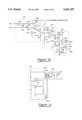
- FIG. 1a is a block diagram of a charging system for an energy-storage capacitor, according to the invention.
- FIGS. 1b and 1c are schematic diagrams exemplary of various functional blocks in the block diagram of FIGS. 1a.
- FIG. 2 is a schematic diagram of an output stage of a two-winding series-parallel energy-storage capacitor charging system, according to the invention.
- FIG. 2a is a "switch-closed" version of the schematic diagram of FIG. 2, showing current flow in the series output configuration.
- FIG. 2b is a "switch-open" version of the schematic diagram of FIG. 2, showing current flow in the parallel output configuration.
- FIG. 3 is a schematic diagram of an output stage of a three-winding series-parallel energy-storage capacitor charging system, according to the invention, illustrating extension of the technique beyond two windings.
- FIG. 3a is a "switch-closed" version of the schematic diagram of FIG. 3 showing current flow for the series output configuration.
- FIG. 3b is a "switch-open" version of the schematic diagram of FIG. 3, showing the parallel configuration current flow.
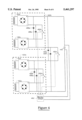
- FIG. 4 is a schematic diagram of a four-winding, two-stage, cascaded series-parallel charging system, according to the invention.
- FIG. 1a is a block diagram of a series-parallel switchable energy-storage capacitor charging system, according to the invention.
- a switching power supply controller 110 (or power oscillator) drives a primary winding 115c of a transformer 115 having two secondary windings 115a and 115b.
- the secondary windings 115a and 115b each have the same number of turns.
- Alternating current (AC) from one of the two secondary windings 15a is rectified by a first rectifier 120a (preferably a full-wave rectifier), while AC current from the other secondary winding 115b is rectified by a second rectifier 120b.
- Each rectifier 120a and 120b has a positive (+) and a negative (-) output.
- a switch 130 is connected from the positive (+) output of the first rectifier 120a to the negative (-) output of the second rectifier 120b.
- the switch is preferably an electronic switch, (such as an FET or bipolar transistor) but may be an electromechanical (e.g., relay) switching device.
- An energy storage capacitor 135 is connected across the positive (+) output of the second rectifier 120b and the negative (-) output of the first rectifier 120a.
- the anode of a first diode 125a is connected to the positive (+) output of the first rectifier 120a, and the cathode of the same diode 125a is connected to the positive (+) output of the second rectifier 120b.
- the anode of a second diode 125b is connected to the negative (-) output of the first rectifier 120a, and the cathode of the same diode 125b is connected to the negative (-) output of the second rectifier 120b.
- a voltage monitor 140 measures the voltage across the energy-storage capacitor 135.
- a feedback signal from the voltage monitor 140 is connected to the switching power supply controller 110. (This assumes a voltage regulated power supply operation on completion of charging. This connection is not necessary if the circuit is operated open loop using a power oscillator to drive the primary winding 115c).
- a level detector 145 senses the voltage level on the energy storage capacitor 135 (via the voltage monitor 140) and closes the switch 130 if the voltage across the capacitor 135 is above a predetermined level. (If there is no other use for a voltage monitor output then the voltage monitor 140 and level detector 145 can be combined into a single block.
- a single switch effects the series-parallel switching of the two windings 115a and 115b (and rectifiers 120a and 120b).
- the switch 130 When the switch 130 is closed, the diodes 125a and 125b are both reverse biased, and are effectively removed from the circuit, placing the two rectifiers (and windings) into a series-connected configuration.
- the switch 130 When the switch 130 is open, the two rectifiers (windings) are effectively connected in parallel, and current from the first rectifier 120a flows through the first diode 125a, into a first terminal of the energy storage capacitor 135, and returns via direct connection to the opposite terminal of the capacitor 135.
- Current from the second rectifier 120b flows directly into the first terminal of the energy storage capacitor 135 and returns via the second diode 125b, which is connected to the opposite terminal of the capacitor 135.
- neither rectifier 120a or 120b is required to withstand current flow or voltage levels greater than those produced by the single winding 115a or 115b, respectively, to which it is connected. It should also be noted that neither diode 125a or 125b is required to carry current or withstand inverse voltage greater than that produced by a single winding (115a or 115b). This potentially reduces the size, cost, and required power dissipation for the diodes and rectifiers as compared to other switching arrangements which need to be sized to accommodate "doubled up" currents and/or voltages. Single-junction rectifiers are limited in their ability to withstand inverse voltage and are commonly matched and connected in series to accommodate higher voltages. The use of multiple rectifiers in FIG.
- FIG. 1b is a schematic diagram including circuits corresponding to the voltage monitor 140, level detector 145 and switch 130.
- the circuits shown are merely exemplary of suitable circuits for performing these functions.
- the voltage monitor 140 comprises a differential amplifier and a voltage divider.
- Two input terminals 141a and 141b to the voltage monitor 140 connect to the more positive (top, as shown in FIG. 1a) and more negative (bottom, as shown in FIG. 1a) sides of the capacitor 135, respectively.
- Resistors 142a and 142b form a voltage divider which scales the (potentially high) voltage across the capacitor 135 down to a level suitable for signal processing.
- the value of the resistor 142a (R) is determined according to the peak voltage which can be expected across the capacitor, and is typically a very large value causing minimal leakage of current from the capacitor (compared to the discharge current).
- An operational amplifier 144 and resistors 142c, 142d, 142e and 142f are connected in a differential amplifier configuration to reject any common-mode voltage present at the input terminals, and to provide a single-ended representation of the voltage across the capacitor 135 at the output of amplifier 144.
- This output voltage is provided as a feedback signal to the switching power supply controller 110 (assuming feedback voltage regulation is used).
- Resistors 142g and 142h form another voltage divider which scales the voltage at the output of the operational amplifier 144 to a level better suited to threshold detection in the level detector 145 (and simultaneously provides an impedance against which a positive feedback resistor therein can provide hysteresis).
- the level detector 145 comprises a differential comparator 147, two resistors 147a and 147b connected as a voltage divider, and a feedback resistor 147c.
- the voltage divider connects to a 5 V reference voltage, providing a reference voltage of about 3.75 volts at the negative input to the differential comparator 147.
- the feedback resistor 147c is connected from the output of the differential comparator 147 to the positive input of the comparator 147, which is in turn connected to the signal from the voltage divider in the voltage monitor 140 (at the junction between the two resistors 142g and 142h).
- the positive feedback provided by the feedback resistor 147c creates a hysteresis band of approximately 20 millivolts in the response of the level detector 145.
- the output of the differential comparator 147 provides the output signal from the level detector 145, which controls the switch 130.
- the switch 130 employs opto-isolation to achieve isolation from the output levels of the charging system.
- the output signal of the level detector 145 drives a light emitting diode (LED) in an opto-isolator 131.
- a resistor 132a limits sets the LED current to about 10 ma.
- the output of the opto-isolator 131 (a phototransistor) is connected in a darlington configuration with a transistor 133 and resistors 132b and 132c and connects to the gate input of an IGBT (insulated gate bipolar transistor, a composite device having MOSFET-like input isolation and a bipolar transistor-like collector and emitter).
- IGBT insulated gate bipolar transistor, a composite device having MOSFET-like input isolation and a bipolar transistor-like collector and emitter.
- a zener diode 132d protects the gate input of the IGBT.
- the collector and emitter 134a and 134b, respectively, of the IGBT act as a directional current switch between the positive output of the first rectifier 120a (FIG. 1a) and the negative output of the second rectifier 120b. Because of the required direction of current flow, the collector 134a connects to the first rectifier 120a and the emitter 134b connects to the second rectifier 120b.
- the switch 130 is an active electronic switch, and since it "floats" with the output stages of the charging system, it requires a floating power supply (connected at points marked FP+ and FP-).
- FIG. 1c is a schematic diagram of a circuit suitable for use as such a floating power supply, and is intended to be merely exemplary of many possible suitable implementations.
- the floating supply is essentially a transformer-coupled DC--DC converter comprising an oscillator 150, a transformer 160 with a primary winding 160a, a feedback winding 160b, and a secondary winding 160c.
- the oscillator 150 (comprising components as shown) operates in conjunction with the primary winding 160a and feedback winding 160b, to provide a driving AC signal into the primary winding 160a.
- the resulting AC signal at the secondary winding 160c is rectified by a diode 162 and filtered by a capacitor 166.
- the output voltage of the supply is limited by a zener diode 164.
- FIGS. 2, 2a, and 2b show the output stages of a two-winding series-parallel charging system for an energy storage capacitor 240 similar to that shown in FIG. 1a, but in greater detail, and including some optional additional elements.
- FIG. 2 is a schematic diagram of the output stage showing circuit details for all components except the switch 230 and monitor circuit 250 (which have been described in detail hereinabove).
- a transformer having two secondary windings 210a and 210b and a single primary winding 210c is used. It is assumed that the primary winding 210c is driven with a suitable AC waveform.
- the secondary windings 210a and 210b are connected via tuned circuits 212a and 212b, respectively, to full wave rectifiers 220a and 220b, respectively.
- the (optional) tuned circuits 212a and 212b serve to optimize the current waveform and energy transfer efficiency delivered through the full-wave rectifiers 220a and 220b, respectively, and to limit surge currents.
- Filter capacitors 225a and 225a' filter the output of rectifier 220a, and filter capacitors 225b and 225b' filter the output of rectifier 220b (These also tend to smooth voltage and current waveforms).
- the positive output of the first full-wave rectifier 220a is connected to the anode of a first diode 235a and to one side of a switch 230b (preferably an electronic switch such as that described hereinabove with respect to FIG. 1b, but drawn as a mechanical switch for simplicity).
- the negative output of the first rectifier 220a is connected directly to the anode of a second diode 235b and indirectly to the negative side of the energy storage capacitor 240 via a filter 245.
- the positive output of the second full-wave rectifier 220b is connected directly to the cathode of the first diode 235a and indirectly to the positive side of the energy storage capacitor 240 via the filter 245.
- the negative output of the second full-wave rectifier 220b is connected to the cathode of the second diode 235b and to the other side of the switch 230b.
- a monitor circuit similar to that shown and described with respect to FIG. 1b, closes the switch 230b when the voltage across the energy storage capacitor 240 exceeds a threshold voltage level.
- the filter 245 is made from a pair of loosely coupled coils wound on a common core and two capacitors, and serves to further smooth the current into the energy storage capacitor. This smoothing of current has several benefits. First, it helps limit peak currents seen by the rectifiers 220a and 220b and the diodes 235a and 235b. Second, it simplifies the monitoring circuit and reduces the hysteresis band required therein. Third, it limits or eliminates both conducted and radiated high-frequency emissions which can cause noise in other parts of the circuit and interference with the operation of other equipment.
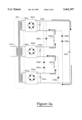
- FIG. 2a is a schematic diagram similar to FIG. 2 (monitor circuit eliminated to reduce illustrative clutter) showing current flow in a series-connected mode with the switch 230 closed (again shown as a mechanical switch).
- the current exits the positive output of the second rectifier 220b and travels through the filter 245, through the capacitor 240, back through the filter 245 and into the negative output of the first rectifier 220a.
- This current via the secondary winding 210a, exits the positive output of the first rectifier 220a, flows through the closed switch 230 and into the negative output of the second rectifier 220b, returning via the secondary winding 210b back to its starting point.
- diodes 235a and 235b are both reverse biased and effectively eliminated from the circuit in this mode of operation. This is illustrated by dashed lines connecting to the diodes.
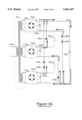
- FIG. 2c is a schematic diagram similar to that of FIG. 2, but showing current flow through the circuit in a parallel mode of operation with the switch 230 open. In this mode, the switch is shown connected via dashed lines, indicating that it is out of circuit in this mode of operation. Again following current flow, current flows out of the positive output of the second rectifier 220b through the filter 245, through the capacitor 240, back through the filter 245 and through the (now forward biased) diode 235b into the negative output of the second rectifier 220b, where it returns via the secondary winding 210b, to its starting point.
- the output stage is connected to the capacitor so that the rectified outputs of the secondary windings are in parallel (switch open--FIG. 2b) up to a threshold voltage across the capacitor, and are in series (switch closed--FIG. 2a) after the threshold has been attained.
- FIG. 3 illustrates an embodiment of the inventive technique in a power supply employing three (or more) secondary windings.
- filter components such as those described with respect to FIGS. 2-2b are omitted, since they are not essential to the inventive switching technique. Even numbers of windings are preferred, to allow intermediate series/parallel switching when four or more windings are used.
- a transformer 310 with three secondary windings 310a, 310b, and 310c, and a single primary winding 310d is assumed to have a suitable AC driving signal at its primary winding 310d.
- the resulting AC waveforms at the first, second, and third secondary windings 310a, 310b, and 310c, are rectified by rectifiers 320a, 320b, and 320c, respectively, and filtered by filer capacitors 325a, 325b, and 325c, respectively.
- the positive output of the first rectifier 320a is connected to the anode of a first diode 335a and to one side of a first switch 330a (preferably an electronic switch).
- the cathode of the first diode 335a is connected to the anode of a second diode 335b.
- the cathode of the second diode 335b is connected to the positive output of the third rectifier 320c, which is further connected to the positive side of an energy storage capacitor 340.
- the positive output of the second rectifier 320b is connected to the anode of a third diode 335c and to one side of a second switch 330b (preferably an electronic switch).
- the cathode of the third diode 335c is connected to the positive output of the third rectifier 320c.
- the negative output of the first rectifier 320a is connected to the negative side of the energy storage capacitor 340, to the anode of a fourth diode 335d and to the anode of a fifth diode 335e.
- the cathode of the fourth diode 335d is connected to the negative output of the second rectifier 320b and to the opposite side of the first switch 330a.
- the cathode of the fifth diode 335e is connected to the anode of a sixth diode 335f.
- the cathode of the sixth diode 335f is connected to the negative output of the third rectifier 320c.
- a monitor circuit 350 monitors the voltage across the capacitor 340 and controls closure of the switches 330a and 330b.
- the "doubled-up" diode pairs 335a/335b and 335e/335f are provided to even up diode drops in the parallel-connected configuration. In other words, currents flowing from/to the second rectifier 320b also experience two diode drops through diodes 335c and 335d.
- each of the "inner” windings would have components and connections similar to those shown for the second winding 310b, each having a single diode in series with each of the rectifier. Since there would be two diode drops for each "inner” winding, the outer windings, which would have components and connections similar to those shown for windings 310a and 310c, would require doubled-up diodes so that current-sharing between the windings will function properly.
- FIG. 3a is a repetition of the schematic of FIG. 3, (monitor circuit omitted to reduce illustrative clutter) showing current flow for a series connected configuration with the switches 330a and 330b closed.
- the switches 330a and 330b closed.
- all of the diodes 335a-f are reverse biased, effectively removing them from the circuits. This is illustrated by showing connections to the diodes as dashed lines.
- FIG. 3b is a schematic diagram similar to FIG. 3a, but showing current flow in a parallel (current-sharing) mode of circuit operation with the switches 330 and 330b open. Since the switches 330a and 330b are effectively out of circuit, connections to the switches 330a and 330b are shown as dashed lines. In the parallel-connected mode, currents from the three windings 310a, 310b, and 310c flow as follows:
- first secondary winding 310a For the first secondary winding 310a, current flows out of the positive output of the first rectifier 320a, through the stacked first and second diodes 335a and 335b, (now joining currents from the second and third secondary windings) through the capacitor 340, (now parting from currents from the second and third secondary windings) into the negative output of the first rectifier 320a, and through the first secondary winding 310a back to its starting point.
- the output stage configuration described hereinabove with respect to FIG. 3 is most useful in the configurations shown, with all of the rectified outputs of the windings switched from a parallel (current-sharing) to a series (enhanced charging voltage) connection.
- FIG. 4 is a schematic diagram of an output configuration for a capacitor charging system which extends the inventive technique to multi-stage switching of binary multiples of windings.
- водем ⁇ ки 410a, 410b, 410c, and 410d of a transformer are arranged into two series-parallel switched pairs 420a and 420b, each configured as described hereinabove with respect to FIG. 1a.
- One series-parallel switched pair 420a utilizes secondary windings 410a and 410b, which are series-parallel switched by two diodes 435a and 435b and a first switch 430a as described in detail hereinabove.
- the other series-parallel switched pair 420b utilizes secondary windings 410c and 410d, which are series-parallel switched by two diodes 435c and 435d and a second switch 430b.
- the two series-parallel switched pairs 420a and 420b are in turn series-parallel switched by two diodes 435e and 435f and a third switch 430c, to charge an energy storage capacitor 440.
- a monitor circuit 450 controls the closures of the three switches.
- the monitor circuit 450 there are two critical voltage thresholds for the monitor circuit 450, one higher than the other. If the voltage is below both thresholds, then the monitor circuit opens all of the switches 430a-c, placing the current from secondary windings 410a and 410b in parallel, the current from secondary windings 410c and 410d in parallel, and the current form each of the pairs of windings (420a and 420b) in parallel with each other. In this way, all four secondary windings 410a-d are effectively connected in parallel to provide four times the charging current which would be available from any one winding alone.
- the monitor circuit 450 can either close switch 430c and open switches 430a and 430b, or it can close switches 430a and 430b and open switch 430c.
- the current from windings 430a and 430b in parallel is connected conducted in series with current from windings 430c and 430d in parallel. This provides twice the current which would be available from any one winding alone at twice the voltage available from any one winding alone.
- the current and voltage results are the same, but are accomplished with the parallel combination of windings 420a and 420b in series and 420c and 420d in series.
- the monitor circuit 450 closes all of the switches 430a-c, effectively placing the current from all of the windings 410a-d in a series-conducting arrangement providing four times the voltage available from any single winding alone at a current equal to that available from each winding alone.
- monitor circuit 450 can be implemented as a pair of level detectors set to different threshold voltages, with one of the level detectors controlling switches 430a and 430b and the other level detector controlling switch 430c.
Landscapes
- Engineering & Computer Science (AREA)
- Power Engineering (AREA)
- Dc-Dc Converters (AREA)
- Charge And Discharge Circuits For Batteries Or The Like (AREA)
Abstract
Description
Claims (19)
Priority Applications (1)
| Application Number | Priority Date | Filing Date | Title |
|---|---|---|---|
| US08/065,994 US5461297A (en) | 1993-05-24 | 1993-05-24 | Series-parallel switchable capacitor charging system |
Applications Claiming Priority (1)
| Application Number | Priority Date | Filing Date | Title |
|---|---|---|---|
| US08/065,994 US5461297A (en) | 1993-05-24 | 1993-05-24 | Series-parallel switchable capacitor charging system |
Publications (1)
| Publication Number | Publication Date |
|---|---|
| US5461297A true US5461297A (en) | 1995-10-24 |
Family
ID=22066572
Family Applications (1)
| Application Number | Title | Priority Date | Filing Date |
|---|---|---|---|
| US08/065,994 Expired - Lifetime US5461297A (en) | 1993-05-24 | 1993-05-24 | Series-parallel switchable capacitor charging system |
Country Status (1)
| Country | Link |
|---|---|
| US (1) | US5461297A (en) |
Cited By (62)
| Publication number | Priority date | Publication date | Assignee | Title |
|---|---|---|---|---|
| US5568035A (en) * | 1993-10-15 | 1996-10-22 | Sony/Tektronix Corporation | Variable-capacitance power supply apparatus |
| US5801931A (en) * | 1994-12-06 | 1998-09-01 | Hitachi, Ltd. | DC power source apparatus that suppresses harmonics |
| WO1999025062A1 (en) * | 1997-11-07 | 1999-05-20 | Sierra Applied Sciences, Inc. | Auto-ranging power supply |
| WO1999030407A1 (en) * | 1997-12-08 | 1999-06-17 | Semi-Tech Design, Inc. | Method and circuit for detection of primary switches status in isolated dc/dc converters |
| US5933338A (en) * | 1997-10-14 | 1999-08-03 | Peco Ii, Inc. | Dual coupled current doubler rectification circuit |
| US5990731A (en) * | 1997-02-04 | 1999-11-23 | Nec Corporation | Input/output protection circuit |
| WO1999063649A1 (en) * | 1998-05-29 | 1999-12-09 | Fronius Schweissmaschinen Produktion Gmbh & Co.Kg | Voltage switch-over device |
| US6087811A (en) * | 1998-12-09 | 2000-07-11 | Analog Modules, Inc. | Pulsed-output power supply with high power factor |
| US6118679A (en) * | 1999-04-26 | 2000-09-12 | Astec International, Limited | Current sharing transformer circuit for power converters |
| US6333619B1 (en) * | 2000-03-15 | 2001-12-25 | Jaime H Chavez | Cyclical battery charger with incremental and decremental current and a method of operation thereof |
| US6352352B1 (en) * | 1998-08-27 | 2002-03-05 | Georg Schletterer | Luminescent container with quick-charging power source |
| EP1278294A1 (en) * | 2001-07-16 | 2003-01-22 | CPAutomation S.A. | An electrical power supply suitable in particular for dc plasma processing |
| US20030080719A1 (en) * | 2001-10-30 | 2003-05-01 | Origin Electric Company, Limited | Capacitor charging method and charging apparatus |
| WO2003071648A3 (en) * | 2002-02-19 | 2003-11-06 | Vector Mfg Ltd | Microprocessor controlled booster apparatus with polarity protection |
| US20040130298A1 (en) * | 2002-02-19 | 2004-07-08 | Michael Krieger | Microprocessor controlled booster apparatus with polarity protection |
| US6798389B1 (en) * | 1999-04-30 | 2004-09-28 | Illinois Tool Works Inc. | Electronic tags incorporating a customer attracting annunciator for use in electronic product information display systems |
| US20050083020A1 (en) * | 2003-10-20 | 2005-04-21 | Baarman David W. | Electrostatic charge storage assembly |
| US20050135130A1 (en) * | 2003-12-17 | 2005-06-23 | Myeong-Ho Gil | Device for detection of power-off |
| US20060192612A1 (en) * | 2005-02-25 | 2006-08-31 | International Business Machines Corporation | Capacitor reliability for multiple-voltage power supply systems |
| US20060279259A1 (en) * | 2005-06-06 | 2006-12-14 | Abb Oy | Method and arrangement for charging capacitors of direct-voltage intermediate circuit of frequency converter |
| US20080048499A1 (en) * | 2004-06-18 | 2008-02-28 | Roman Litovsky | Controlling a Power Converter |
| WO2006099759A3 (en) * | 2005-03-24 | 2008-04-10 | Oerlikon Trading Ag | Vacuum plasma generator |
| FR2918816A1 (en) * | 2007-07-11 | 2009-01-16 | Renault Sas | Electric power supplying circuit for corona effect or dielectric barrier discharge type plasma reactor of motor vehicle, has switching circuit controlling discharge of storage unit towards reactor when switching circuit is in close state |
| US20090091302A1 (en) * | 2007-10-04 | 2009-04-09 | Ileana Rusan | Method of charging and discharging of supercapacitors without the use of converters or chargers |
| US20090108681A1 (en) * | 2007-10-29 | 2009-04-30 | Bose Corporation | Automatic Power Source Configuration |
| US20090110214A1 (en) * | 2007-10-30 | 2009-04-30 | Litovsky Roman N | Controlled charging and use of power source |
| EP2083498A1 (en) * | 2000-01-28 | 2009-07-29 | Cummins Generator Technologies Limited | An AC power generating system |
| US20100007307A1 (en) * | 2008-07-09 | 2010-01-14 | Access Business Group International Llc | Wireless charging system |
| CN101834538A (en) * | 2010-05-21 | 2010-09-15 | 浙江大学 | Multi-input rectifying circuit for distributed power generation |
| US20100244773A1 (en) * | 2009-03-27 | 2010-09-30 | Gm Global Technology Operations, Inc. | Unity power factor isolated single phase matrix converter battery charger |
| US20110031927A1 (en) * | 2009-08-05 | 2011-02-10 | Gm Global Technology Operations, Inc. | Charging system with galvanic isolation and multiple operating modes |
| US20110031930A1 (en) * | 2009-08-05 | 2011-02-10 | Gm Global Technology Operations, Inc. | Systems and methods for bi-directional energy delivery with galvanic isolation |
| US20110115285A1 (en) * | 2009-11-19 | 2011-05-19 | Gm Global Technology Operations, Inc. | Systems and methods for commutating inductor current using a matrix converter |
| US20110227407A1 (en) * | 2010-03-16 | 2011-09-22 | Gm Global Technology Operations, Inc. | Systems and methods for deactivating a matrix converter |
| US20120250377A1 (en) * | 2011-04-04 | 2012-10-04 | Samsung Electronics Co., Ltd | Voltage adjusting circuit and contactless card and contactless card system which include the same |
| US8462528B2 (en) | 2010-07-19 | 2013-06-11 | GM Global Technology Operations LLC | Systems and methods for reducing transient voltage spikes in matrix converters |
| US8467197B2 (en) | 2010-11-08 | 2013-06-18 | GM Global Technology Operations LLC | Systems and methods for compensating for electrical converter nonlinearities |
| US8587962B2 (en) | 2010-11-08 | 2013-11-19 | GM Global Technology Operations LLC | Compensation for electrical converter nonlinearities |
| US8599577B2 (en) | 2010-11-08 | 2013-12-03 | GM Global Technology Operations LLC | Systems and methods for reducing harmonic distortion in electrical converters |
| US8614564B2 (en) | 2010-11-18 | 2013-12-24 | GM Global Technology Operations LLS | Systems and methods for providing power to a load based upon a control strategy |
| US8643340B1 (en) * | 2009-09-29 | 2014-02-04 | Cirrus Logic, Inc. | Powering a circuit by alternating power supply connections in series and parallel with a storage capacitor |
| US8737097B1 (en) * | 2012-11-29 | 2014-05-27 | Yaskawa America, Inc. | Electronically isolated method for an auto transformer 12-pulse rectification scheme suitable for use with variable frequency drives |
| US8829858B2 (en) | 2011-05-31 | 2014-09-09 | GM Global Technology Operations LLC | Systems and methods for initializing a charging system |
| US8860379B2 (en) | 2011-04-20 | 2014-10-14 | GM Global Technology Operations LLC | Discharging a DC bus capacitor of an electrical converter system |
| US8878495B2 (en) | 2011-08-31 | 2014-11-04 | GM Global Technology Operations LLC | Systems and methods for providing power to a load based upon a control strategy |
| US9008275B2 (en) | 2012-05-01 | 2015-04-14 | Analogic Corporation | Voltage switching in an imaging modality that utilizes radiation to image an object |
| US20150210170A1 (en) * | 2007-10-25 | 2015-07-30 | Toyota Jidosha Kabushiki Kaisha | Electrical powered vehicle and power feeding device for vehicle |
| US20160190943A1 (en) * | 2013-10-29 | 2016-06-30 | Massachusetts Institute Of Technology | Switched-Capacitor Split Drive Transformer Power Conversion Circuit |
| US9770991B2 (en) | 2013-05-31 | 2017-09-26 | GM Global Technology Operations LLC | Systems and methods for initializing a charging system |
| US20170366022A1 (en) * | 2016-06-15 | 2017-12-21 | Schneider Electric It Corporation | Stack dc power supply battery charger |
| US9929585B2 (en) | 2014-09-03 | 2018-03-27 | Kettering University | Power transfer system |
| WO2018158453A1 (en) | 2017-03-03 | 2018-09-07 | Abb Schweiz Ag | Battery charger for traction vehicle |
| US20190222129A1 (en) * | 2018-01-15 | 2019-07-18 | Queen's University At Kingston | Power Converter Topologies and Control Methods for Wide Input and Output Voltage Ranges |
| WO2019199299A1 (en) * | 2018-04-11 | 2019-10-17 | Aerojet Rocketdyne, Inc. | Power converter including a recirculating snubber |
| US10644503B2 (en) | 2013-10-29 | 2020-05-05 | Massachusetts Institute Of Technology | Coupled split path power conversion architecture |
| US10777967B2 (en) * | 2017-05-03 | 2020-09-15 | Analog Modules, Inc. | Pulsed laser diode drivers and methods |
| EP3772169A1 (en) * | 2019-08-02 | 2021-02-03 | Hamilton Sundstrand Corporation | Four-mode tap-switching transformer rectifier |
| USRE48659E1 (en) | 2010-12-24 | 2021-07-27 | Toyota Jidosha Kabushiki Kaisha | Non-contact charging system, non-contact charging method, non-contact charging type vehicle, and non-contact charging management apparatus |
| CN113193749A (en) * | 2021-06-11 | 2021-07-30 | 上海空间电源研究所 | Wide-range high-voltage flexible direct-current combined conversion topology |
| US11296581B2 (en) * | 2018-07-23 | 2022-04-05 | Nanjing Chervon Industry Co., Ltd. | Power tool |
| WO2023050656A1 (en) * | 2021-09-29 | 2023-04-06 | 西安领充创享新能源科技有限公司 | Method and apparatus for controlling series-parallel switching circuit, and controller and storage medium |
| US11837848B2 (en) | 2019-09-30 | 2023-12-05 | Analog Modules, Inc. | High PRF, high efficiency laser diode driver power supply |
Citations (11)
| Publication number | Priority date | Publication date | Assignee | Title |
|---|---|---|---|---|
| US3106672A (en) * | 1961-09-29 | 1963-10-08 | Bell Telephone Labor Inc | Output voltage control for power conversion apparatus |
| US3654537A (en) * | 1970-04-29 | 1972-04-04 | Westinghouse Electric Corp | High efficiency power supply for charging capacitors in steps |
| US3694731A (en) * | 1971-06-18 | 1972-09-26 | Motorola Inc | Multiple mode vehicle power supply system |
| US3984750A (en) * | 1974-06-04 | 1976-10-05 | Robert Bosch G.M.B.H. | Alternator-rectifier unit with phase winding and rectifier sets subject to series-parallel switching |
| US4009431A (en) * | 1975-09-08 | 1977-02-22 | General Motors Corporation | Series parallel transition for power supply |
| JPS5586380A (en) * | 1978-12-22 | 1980-06-30 | Hitachi Ltd | Power supply device for energizing coil |
| SU907720A1 (en) * | 1980-05-30 | 1982-02-23 | Украинский Государственный Проектно-Технологический И Экспериментальный Институт "Укроргстанкинпром" | Device for control of series-parallel connected thyristors |
| US4339704A (en) * | 1980-07-07 | 1982-07-13 | General Electric Company | Series parallel transition for power supply |
| US4429357A (en) * | 1980-06-25 | 1984-01-31 | Bbc Brown, Boveri & Company Limited | Method for placing into operation a series connected group of static power converters of a high voltage direct-current transmission installation |
| JPH01286800A (en) * | 1988-05-12 | 1989-11-17 | Seiko Instr Inc | Charging mechanism |
| US5398182A (en) * | 1993-07-20 | 1995-03-14 | Namco Controls Corporation | Power supply |
-
1993
- 1993-05-24 US US08/065,994 patent/US5461297A/en not_active Expired - Lifetime
Patent Citations (11)
| Publication number | Priority date | Publication date | Assignee | Title |
|---|---|---|---|---|
| US3106672A (en) * | 1961-09-29 | 1963-10-08 | Bell Telephone Labor Inc | Output voltage control for power conversion apparatus |
| US3654537A (en) * | 1970-04-29 | 1972-04-04 | Westinghouse Electric Corp | High efficiency power supply for charging capacitors in steps |
| US3694731A (en) * | 1971-06-18 | 1972-09-26 | Motorola Inc | Multiple mode vehicle power supply system |
| US3984750A (en) * | 1974-06-04 | 1976-10-05 | Robert Bosch G.M.B.H. | Alternator-rectifier unit with phase winding and rectifier sets subject to series-parallel switching |
| US4009431A (en) * | 1975-09-08 | 1977-02-22 | General Motors Corporation | Series parallel transition for power supply |
| JPS5586380A (en) * | 1978-12-22 | 1980-06-30 | Hitachi Ltd | Power supply device for energizing coil |
| SU907720A1 (en) * | 1980-05-30 | 1982-02-23 | Украинский Государственный Проектно-Технологический И Экспериментальный Институт "Укроргстанкинпром" | Device for control of series-parallel connected thyristors |
| US4429357A (en) * | 1980-06-25 | 1984-01-31 | Bbc Brown, Boveri & Company Limited | Method for placing into operation a series connected group of static power converters of a high voltage direct-current transmission installation |
| US4339704A (en) * | 1980-07-07 | 1982-07-13 | General Electric Company | Series parallel transition for power supply |
| JPH01286800A (en) * | 1988-05-12 | 1989-11-17 | Seiko Instr Inc | Charging mechanism |
| US5398182A (en) * | 1993-07-20 | 1995-03-14 | Namco Controls Corporation | Power supply |
Cited By (96)
| Publication number | Priority date | Publication date | Assignee | Title |
|---|---|---|---|---|
| US5568035A (en) * | 1993-10-15 | 1996-10-22 | Sony/Tektronix Corporation | Variable-capacitance power supply apparatus |
| US5801931A (en) * | 1994-12-06 | 1998-09-01 | Hitachi, Ltd. | DC power source apparatus that suppresses harmonics |
| US5990731A (en) * | 1997-02-04 | 1999-11-23 | Nec Corporation | Input/output protection circuit |
| US5933338A (en) * | 1997-10-14 | 1999-08-03 | Peco Ii, Inc. | Dual coupled current doubler rectification circuit |
| WO1999025062A1 (en) * | 1997-11-07 | 1999-05-20 | Sierra Applied Sciences, Inc. | Auto-ranging power supply |
| US6011704A (en) * | 1997-11-07 | 2000-01-04 | Sierra Applied Sciences, Inc. | Auto-ranging power supply |
| US6456106B1 (en) | 1997-12-08 | 2002-09-24 | Srmos, Inc. | Method and circuit for detection of primary switches status in isolated DC/DC converters |
| WO1999030407A1 (en) * | 1997-12-08 | 1999-06-17 | Semi-Tech Design, Inc. | Method and circuit for detection of primary switches status in isolated dc/dc converters |
| US6369548B1 (en) | 1998-05-29 | 2002-04-09 | Fronius Schweissmaschinen Produktion Gmbh & Co. Kg | Voltage switch-over device |
| WO1999063649A1 (en) * | 1998-05-29 | 1999-12-09 | Fronius Schweissmaschinen Produktion Gmbh & Co.Kg | Voltage switch-over device |
| US6352352B1 (en) * | 1998-08-27 | 2002-03-05 | Georg Schletterer | Luminescent container with quick-charging power source |
| US6087811A (en) * | 1998-12-09 | 2000-07-11 | Analog Modules, Inc. | Pulsed-output power supply with high power factor |
| US6118679A (en) * | 1999-04-26 | 2000-09-12 | Astec International, Limited | Current sharing transformer circuit for power converters |
| US6798389B1 (en) * | 1999-04-30 | 2004-09-28 | Illinois Tool Works Inc. | Electronic tags incorporating a customer attracting annunciator for use in electronic product information display systems |
| EP2083498A1 (en) * | 2000-01-28 | 2009-07-29 | Cummins Generator Technologies Limited | An AC power generating system |
| US6333619B1 (en) * | 2000-03-15 | 2001-12-25 | Jaime H Chavez | Cyclical battery charger with incremental and decremental current and a method of operation thereof |
| EP1278294A1 (en) * | 2001-07-16 | 2003-01-22 | CPAutomation S.A. | An electrical power supply suitable in particular for dc plasma processing |
| US6567278B2 (en) | 2001-07-16 | 2003-05-20 | Cp Automation S.A. | Electrical power supply suitable in particular for DC plasma processing |
| US6737847B2 (en) * | 2001-10-30 | 2004-05-18 | Origin Electric Company, Limited | Capacitor charging method and charging apparatus |
| US20030080719A1 (en) * | 2001-10-30 | 2003-05-01 | Origin Electric Company, Limited | Capacitor charging method and charging apparatus |
| WO2003071648A3 (en) * | 2002-02-19 | 2003-11-06 | Vector Mfg Ltd | Microprocessor controlled booster apparatus with polarity protection |
| US20040130298A1 (en) * | 2002-02-19 | 2004-07-08 | Michael Krieger | Microprocessor controlled booster apparatus with polarity protection |
| US7656118B2 (en) | 2002-02-19 | 2010-02-02 | Black & Decker Inc. | Microprocessor controlled booster apparatus with polarity protection |
| US7345450B2 (en) | 2002-02-19 | 2008-03-18 | V Ector Products, Inc. | Microprocessor controlled booster apparatus with polarity protection |
| US20080203967A1 (en) * | 2002-02-19 | 2008-08-28 | Vector Products, Inc. | Microprocessor controlled booster apparatus with polarity protection |
| US20050083020A1 (en) * | 2003-10-20 | 2005-04-21 | Baarman David W. | Electrostatic charge storage assembly |
| US20050135130A1 (en) * | 2003-12-17 | 2005-06-23 | Myeong-Ho Gil | Device for detection of power-off |
| US7285989B2 (en) * | 2003-12-17 | 2007-10-23 | Samsung Electronics Co., Ltd. | Device for detection of power-off |
| US20080048499A1 (en) * | 2004-06-18 | 2008-02-28 | Roman Litovsky | Controlling a Power Converter |
| US7880330B2 (en) | 2004-06-18 | 2011-02-01 | Bose Corporation | Controlling a power converter |
| US20060192612A1 (en) * | 2005-02-25 | 2006-08-31 | International Business Machines Corporation | Capacitor reliability for multiple-voltage power supply systems |
| US7113006B2 (en) | 2005-02-25 | 2006-09-26 | International Business Machines Corporation | Capacitor reliability for multiple-voltage power supply systems |
| WO2006099759A3 (en) * | 2005-03-24 | 2008-04-10 | Oerlikon Trading Ag | Vacuum plasma generator |
| US20060279259A1 (en) * | 2005-06-06 | 2006-12-14 | Abb Oy | Method and arrangement for charging capacitors of direct-voltage intermediate circuit of frequency converter |
| US7417408B2 (en) * | 2005-06-06 | 2008-08-26 | Abb Oy | Method and arrangement for charging capacitors of direct-voltage intermediate circuit of frequency converter |
| FR2918816A1 (en) * | 2007-07-11 | 2009-01-16 | Renault Sas | Electric power supplying circuit for corona effect or dielectric barrier discharge type plasma reactor of motor vehicle, has switching circuit controlling discharge of storage unit towards reactor when switching circuit is in close state |
| US20090091302A1 (en) * | 2007-10-04 | 2009-04-09 | Ileana Rusan | Method of charging and discharging of supercapacitors without the use of converters or chargers |
| US7750606B2 (en) * | 2007-10-04 | 2010-07-06 | Honeywell International Inc. | Method of charging and discharging of supercapacitors without the use of converters or chargers |
| US20150210170A1 (en) * | 2007-10-25 | 2015-07-30 | Toyota Jidosha Kabushiki Kaisha | Electrical powered vehicle and power feeding device for vehicle |
| US9421868B2 (en) * | 2007-10-25 | 2016-08-23 | Toyota Jidosha Kabushiki Kaisha | Electrical powered vehicle and power feeding device for vehicle |
| US20150251546A1 (en) * | 2007-10-25 | 2015-09-10 | Toyota Jidosha Kabushiki Kaisha | Electrical powered vehicle and power feeding device for vehicle |
| US7656061B2 (en) | 2007-10-29 | 2010-02-02 | Bose Corporation | Automatic power source configuration |
| US20090108681A1 (en) * | 2007-10-29 | 2009-04-30 | Bose Corporation | Automatic Power Source Configuration |
| US7888907B2 (en) | 2007-10-30 | 2011-02-15 | Bose Corporation | Controlled charging and use of power source |
| US20090110214A1 (en) * | 2007-10-30 | 2009-04-30 | Litovsky Roman N | Controlled charging and use of power source |
| US9143003B2 (en) | 2008-07-09 | 2015-09-22 | Access Business Group International Llc | Wireless charging system |
| US8638062B2 (en) | 2008-07-09 | 2014-01-28 | Access Business Group International Llc | Wireless charging system |
| US20100007307A1 (en) * | 2008-07-09 | 2010-01-14 | Access Business Group International Llc | Wireless charging system |
| US8531153B2 (en) | 2008-07-09 | 2013-09-10 | Access Business Group International Llc | Wireless charging system |
| US20100244773A1 (en) * | 2009-03-27 | 2010-09-30 | Gm Global Technology Operations, Inc. | Unity power factor isolated single phase matrix converter battery charger |
| US20110031930A1 (en) * | 2009-08-05 | 2011-02-10 | Gm Global Technology Operations, Inc. | Systems and methods for bi-directional energy delivery with galvanic isolation |
| US20110031927A1 (en) * | 2009-08-05 | 2011-02-10 | Gm Global Technology Operations, Inc. | Charging system with galvanic isolation and multiple operating modes |
| US8350523B2 (en) | 2009-08-05 | 2013-01-08 | GM Global Technology Operations LLC | Charging system with galvanic isolation and multiple operating modes |
| US8466658B2 (en) | 2009-08-05 | 2013-06-18 | GM Global Technology Operations LLC | Systems and methods for bi-directional energy delivery with galvanic isolation |
| US8643340B1 (en) * | 2009-09-29 | 2014-02-04 | Cirrus Logic, Inc. | Powering a circuit by alternating power supply connections in series and parallel with a storage capacitor |
| US20110115285A1 (en) * | 2009-11-19 | 2011-05-19 | Gm Global Technology Operations, Inc. | Systems and methods for commutating inductor current using a matrix converter |
| US8288887B2 (en) | 2009-11-19 | 2012-10-16 | GM Global Technology Operations LLC | Systems and methods for commutating inductor current using a matrix converter |
| US20110227407A1 (en) * | 2010-03-16 | 2011-09-22 | Gm Global Technology Operations, Inc. | Systems and methods for deactivating a matrix converter |
| US8410635B2 (en) | 2010-03-16 | 2013-04-02 | GM Global Technology Operations LLC | Systems and methods for deactivating a matrix converter |
| CN101834538A (en) * | 2010-05-21 | 2010-09-15 | 浙江大学 | Multi-input rectifying circuit for distributed power generation |
| US8462528B2 (en) | 2010-07-19 | 2013-06-11 | GM Global Technology Operations LLC | Systems and methods for reducing transient voltage spikes in matrix converters |
| US8599577B2 (en) | 2010-11-08 | 2013-12-03 | GM Global Technology Operations LLC | Systems and methods for reducing harmonic distortion in electrical converters |
| US8587962B2 (en) | 2010-11-08 | 2013-11-19 | GM Global Technology Operations LLC | Compensation for electrical converter nonlinearities |
| US8467197B2 (en) | 2010-11-08 | 2013-06-18 | GM Global Technology Operations LLC | Systems and methods for compensating for electrical converter nonlinearities |
| US8614564B2 (en) | 2010-11-18 | 2013-12-24 | GM Global Technology Operations LLS | Systems and methods for providing power to a load based upon a control strategy |
| USRE48659E1 (en) | 2010-12-24 | 2021-07-27 | Toyota Jidosha Kabushiki Kaisha | Non-contact charging system, non-contact charging method, non-contact charging type vehicle, and non-contact charging management apparatus |
| US8891270B2 (en) * | 2011-04-04 | 2014-11-18 | Samsung Electronics Co., Ltd. | Voltage adjusting circuit and contactless card and contactless card system which include the same |
| US20150061389A1 (en) * | 2011-04-04 | 2015-03-05 | Samsung Electronics Co., Ltd. | Voltage adjusting circuit and contactless card and contactless card system which include the same |
| US20120250377A1 (en) * | 2011-04-04 | 2012-10-04 | Samsung Electronics Co., Ltd | Voltage adjusting circuit and contactless card and contactless card system which include the same |
| US9178362B2 (en) * | 2011-04-04 | 2015-11-03 | Samsung Electronics Co., Ltd. | Voltage adjusting circuit and contactless card and contactless card system which include the same |
| US8860379B2 (en) | 2011-04-20 | 2014-10-14 | GM Global Technology Operations LLC | Discharging a DC bus capacitor of an electrical converter system |
| US8829858B2 (en) | 2011-05-31 | 2014-09-09 | GM Global Technology Operations LLC | Systems and methods for initializing a charging system |
| US8878495B2 (en) | 2011-08-31 | 2014-11-04 | GM Global Technology Operations LLC | Systems and methods for providing power to a load based upon a control strategy |
| US9008275B2 (en) | 2012-05-01 | 2015-04-14 | Analogic Corporation | Voltage switching in an imaging modality that utilizes radiation to image an object |
| US8737097B1 (en) * | 2012-11-29 | 2014-05-27 | Yaskawa America, Inc. | Electronically isolated method for an auto transformer 12-pulse rectification scheme suitable for use with variable frequency drives |
| US9770991B2 (en) | 2013-05-31 | 2017-09-26 | GM Global Technology Operations LLC | Systems and methods for initializing a charging system |
| US9825545B2 (en) * | 2013-10-29 | 2017-11-21 | Massachusetts Institute Of Technology | Switched-capacitor split drive transformer power conversion circuit |
| US20160190943A1 (en) * | 2013-10-29 | 2016-06-30 | Massachusetts Institute Of Technology | Switched-Capacitor Split Drive Transformer Power Conversion Circuit |
| US10644503B2 (en) | 2013-10-29 | 2020-05-05 | Massachusetts Institute Of Technology | Coupled split path power conversion architecture |
| US9929585B2 (en) | 2014-09-03 | 2018-03-27 | Kettering University | Power transfer system |
| US10243376B2 (en) * | 2016-06-15 | 2019-03-26 | Schneider Electric It Corporation | Stack DC power supply battery charger |
| US20170366022A1 (en) * | 2016-06-15 | 2017-12-21 | Schneider Electric It Corporation | Stack dc power supply battery charger |
| WO2018158453A1 (en) | 2017-03-03 | 2018-09-07 | Abb Schweiz Ag | Battery charger for traction vehicle |
| US10777967B2 (en) * | 2017-05-03 | 2020-09-15 | Analog Modules, Inc. | Pulsed laser diode drivers and methods |
| US10944329B2 (en) * | 2018-01-15 | 2021-03-09 | Queen's University At Kingston | Power converter topologies and control methods for wide input and output voltage ranges |
| US20190222129A1 (en) * | 2018-01-15 | 2019-07-18 | Queen's University At Kingston | Power Converter Topologies and Control Methods for Wide Input and Output Voltage Ranges |
| CN112219346A (en) * | 2018-04-11 | 2021-01-12 | 航天喷气发动机洛克达因股份有限公司 | Power converter including a recirculation buffer |
| WO2019199299A1 (en) * | 2018-04-11 | 2019-10-17 | Aerojet Rocketdyne, Inc. | Power converter including a recirculating snubber |
| JP2021521763A (en) * | 2018-04-11 | 2021-08-26 | エアロジェット ロケットダイン インコーポレイテッド | Power converter with recirculation snubber technology |
| US11239745B2 (en) | 2018-04-11 | 2022-02-01 | Aerojet Rocketdyne, Inc | Power converter including a recirculating snubber |
| US11296581B2 (en) * | 2018-07-23 | 2022-04-05 | Nanjing Chervon Industry Co., Ltd. | Power tool |
| EP3772169A1 (en) * | 2019-08-02 | 2021-02-03 | Hamilton Sundstrand Corporation | Four-mode tap-switching transformer rectifier |
| US11121638B2 (en) | 2019-08-02 | 2021-09-14 | Hamilton Sundstrand Corporation | Four-mode tap-switching transformer rectifier |
| US11837848B2 (en) | 2019-09-30 | 2023-12-05 | Analog Modules, Inc. | High PRF, high efficiency laser diode driver power supply |
| CN113193749A (en) * | 2021-06-11 | 2021-07-30 | 上海空间电源研究所 | Wide-range high-voltage flexible direct-current combined conversion topology |
| WO2023050656A1 (en) * | 2021-09-29 | 2023-04-06 | 西安领充创享新能源科技有限公司 | Method and apparatus for controlling series-parallel switching circuit, and controller and storage medium |
Similar Documents
| Publication | Publication Date | Title |
|---|---|---|
| US5461297A (en) | Series-parallel switchable capacitor charging system | |
| US5930122A (en) | Inverter and DC power supply apparatus with inverter used therein | |
| EP0028591B1 (en) | Method of uninterrupted operation of a current supply installation and apparatus for the method | |
| JPS648366B2 (en) | ||
| US5168435A (en) | Converter | |
| CA1302494C (en) | Active snubber structure and method for an electronic power inverter | |
| US5798630A (en) | Switching power circuit to supply electric-vehicle battery charger with high-frequency power | |
| CA1276035C (en) | Static inverter with an overcurrent circuit upon a short circuit | |
| US4669039A (en) | Circuit arrangement for autoconverters | |
| EP0538227A1 (en) | Welding current source for alternating-current arc welding | |
| US5369563A (en) | Fast turn-off circuit for use with an AC bridge circuit | |
| EP0223293B1 (en) | Power-supply circuit | |
| JPH10189286A (en) | Pulse power supply device for electron tube | |
| US5907463A (en) | Overcurrent protection circuit | |
| US3938026A (en) | Circuit for the simultaneous ignition of a plurality of thyristors | |
| KR940003774B1 (en) | Power supply circuit | |
| JPH06245501A (en) | Power device | |
| EP0684754B1 (en) | A power supply circuit, particularly for motor vehicles | |
| CA1268518A (en) | Power generator | |
| RU2109394C1 (en) | Quasi-resonance constant voltage converter with switching- over under zero voltage | |
| SU1293781A1 (en) | Device for arc welding | |
| US5523935A (en) | AC/DC voltage converter | |
| SU1056160A1 (en) | Secondary protected d.c. voltage source | |
| JPH07308028A (en) | Charger for series battery | |
| SU1483568A1 (en) | Multichannel converter for charging capacitive charge integrators |
Legal Events
| Date | Code | Title | Description |
|---|---|---|---|
| AS | Assignment |
Owner name: ANALOG MODULES, INC. Free format text: ASSIGNMENT OF ASSIGNORS INTEREST;ASSIGNOR:CRAWFORD, IAN D.;REEL/FRAME:006586/0241 Effective date: 19930518 |
|
| STPP | Information on status: patent application and granting procedure in general |
Free format text: APPLICATION UNDERGOING PREEXAM PROCESSING |
|
| FPAY | Fee payment |
Year of fee payment: 4 |
|
| FEPP | Fee payment procedure |
Free format text: PAT HOLDER NO LONGER CLAIMS SMALL ENTITY STATUS, ENTITY STATUS SET TO UNDISCOUNTED (ORIGINAL EVENT CODE: STOL); ENTITY STATUS OF PATENT OWNER: LARGE ENTITY |
|
| FEPP | Fee payment procedure |
Free format text: PAT HOLDER CLAIMS SMALL ENTITY STATUS, ENTITY STATUS SET TO SMALL (ORIGINAL EVENT CODE: LTOS); ENTITY STATUS OF PATENT OWNER: LARGE ENTITY |
|
| FPAY | Fee payment |
Year of fee payment: 8 |
|
| AS | Assignment |
Owner name: SUNTRUST BANK, AS ADMINISTRATIVE AGENT, GEORGIA Free format text: SECURITY AGREEMENT;ASSIGNORS:THERMAL STRUCTURES, INC.;ANALOG MODULES, INC.;JETSEAL, INC.;AND OTHERS;REEL/FRAME:013678/0134 Effective date: 20030515 |
|
| FEPP | Fee payment procedure |
Free format text: PAT HOLDER NO LONGER CLAIMS SMALL ENTITY STATUS, ENTITY STATUS SET TO UNDISCOUNTED (ORIGINAL EVENT CODE: STOL); ENTITY STATUS OF PATENT OWNER: LARGE ENTITY |
|
| FPAY | Fee payment |
Year of fee payment: 12 |