US20030198064A1 - Device and method of commutation control for an isolated boost converter - Google Patents
Device and method of commutation control for an isolated boost converter Download PDFInfo
- Publication number
- US20030198064A1 US20030198064A1 US10/345,894 US34589403A US2003198064A1 US 20030198064 A1 US20030198064 A1 US 20030198064A1 US 34589403 A US34589403 A US 34589403A US 2003198064 A1 US2003198064 A1 US 2003198064A1
- Authority
- US
- United States
- Prior art keywords
- current
- transformer
- switches
- inductor
- switch
- Prior art date
- Legal status (The legal status is an assumption and is not a legal conclusion. Google has not performed a legal analysis and makes no representation as to the accuracy of the status listed.)
- Granted
Links
Images


Classifications
-
- H—ELECTRICITY
- H02—GENERATION; CONVERSION OR DISTRIBUTION OF ELECTRIC POWER
- H02M—APPARATUS FOR CONVERSION BETWEEN AC AND AC, BETWEEN AC AND DC, OR BETWEEN DC AND DC, AND FOR USE WITH MAINS OR SIMILAR POWER SUPPLY SYSTEMS; CONVERSION OF DC OR AC INPUT POWER INTO SURGE OUTPUT POWER; CONTROL OR REGULATION THEREOF
- H02M3/00—Conversion of dc power input into dc power output
- H02M3/22—Conversion of dc power input into dc power output with intermediate conversion into ac
- H02M3/24—Conversion of dc power input into dc power output with intermediate conversion into ac by static converters
- H02M3/28—Conversion of dc power input into dc power output with intermediate conversion into ac by static converters using discharge tubes with control electrode or semiconductor devices with control electrode to produce the intermediate ac
- H02M3/325—Conversion of dc power input into dc power output with intermediate conversion into ac by static converters using discharge tubes with control electrode or semiconductor devices with control electrode to produce the intermediate ac using devices of a triode or a transistor type requiring continuous application of a control signal
- H02M3/335—Conversion of dc power input into dc power output with intermediate conversion into ac by static converters using discharge tubes with control electrode or semiconductor devices with control electrode to produce the intermediate ac using devices of a triode or a transistor type requiring continuous application of a control signal using semiconductor devices only
- H02M3/33569—Conversion of dc power input into dc power output with intermediate conversion into ac by static converters using discharge tubes with control electrode or semiconductor devices with control electrode to produce the intermediate ac using devices of a triode or a transistor type requiring continuous application of a control signal using semiconductor devices only having several active switching elements
- H02M3/33576—Conversion of dc power input into dc power output with intermediate conversion into ac by static converters using discharge tubes with control electrode or semiconductor devices with control electrode to produce the intermediate ac using devices of a triode or a transistor type requiring continuous application of a control signal using semiconductor devices only having several active switching elements having at least one active switching element at the secondary side of an isolation transformer
Definitions
- the present invention relates generally to the field of direct current-to-direct current (DC/DC) converters, and more particularly to commutation control schemes for an isolated boost converter.
- DC/DC direct current-to-direct current
- Isolated DC/DC converters for converting a low voltage direct current (dc) power source, such as a 12 volt battery, to a high voltage DC power source, such as a 300V traction battery are known in the art.
- a low voltage direct current (dc) power source such as a 12 volt battery
- a high voltage DC power source such as a 300V traction battery
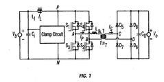
- FIG. 1 An example of such a converter in the form of an isolated boost DC/DC converter is illustrated in FIG. 1.
- an inductor L f is used as the current source at the low voltage side V b to reduce the RMS (root-mean-square) current rating of low voltage transistors S 1 , S 2 , S 3 , and S 4 .
- the low voltage transistors S 1 , S 2 , S 3 , and S 4 operate as an inverter to convert DC current (voltage) to a high frequency alternating current (ac) (voltage).
- An isolation transformer T steps up the voltage to a higher level by the turns ratio, while providing galvanic isolation for safety regulations.
- Diodes D 5 , D 6 , D 7 , and D 8 operate as a rectifier to convert the high frequency AC current (voltage) to the desired high DC voltage.
- the function is basically to chop the low voltage from the V b energy source, such as the 12 volt battery voltage, into the AC voltage.
- the inductor L f is provided to limit the inrush current.
- the inductor is provided to regulate the input current to limit the current from the battery.
- the converter also includes the transformer T, which posses non-zero leakage inductance L lk . As more fully explained below, this non-zero leakage inductance creates a problem whenever the switch states are changed.
- Ldl/dt there is a voltage across the inductor referred to as Ldl/dt, i.e., the inductance L times the rate of current change dl/dt.
- the change of the polarity of the current in the leakage inductance occurs as the switches are turned on and off at a level of micro-seconds. Therefore, if the input current is, for example, 150 amperes, it becomes negative 150 amperes in one or two micro-seconds.
- the dl/dt is very high, and if the inductance leakage is not at zero, the voltage can be sizeable.
- the leakage inductance associated with the power stage of a DC/DC converter is typically in the range of ten microhenries.
- the current is reversed 300 amperes from plus 150 amperes to negative 150 amperes in half a micro-second, if the leakage inductance is, for example, four or five microhenries, the voltage is in the range of about 2000 volts.
- the switches S 1 , S 2 , S 3 , and S 4 which are power transistors, have a voltage limit, and it can be very difficult for these transistors to withstand such a high voltage spike.
- FIG. 1 A typical approach to dealing with this problem is a passive clamp circuit, as shown in FIG. 1, which is basically a capacitor with a diode. When the voltage is beyond the capacitor voltage, the diode conducts and diverts the energy to the capacitor to clamp out the voltage spike. In that way, the switches S 1 , S 2 , S 3 , and S 4 can be protected from an over-voltage situation.
- L lk energy that is transferred from the leakage inductance L lk is stored in the clamp capacitor. That energy will charge up the capacitor unless a way is provided to deplete the capacitor or to consume the energy each time the transistors are switched.
- an embodiment of the present invention provides a soft switching commutation control scheme for isolated boost converters in which current in the leakage inductance of the transformer is preset to significantly reduce the mismatch current with the inductor during commutation, thereby significantly reducing the power rating for the voltage clamp circuit for the low voltage inverter.
- a unique control logic implements a partial resonant and then freewheeling operation from the high voltage side to achieve leakage current presetting.
- This control scheme makes use of parasitic parameters, such as transformer leakage inductance and transistor output junction capacitors, and the operation is insensitive to these parasitic parameters. Natural soft switching is achieved for the transistors at the high voltage side, which leads to lower switching loss and lower electromagnetic interference (EMI).
- EMI electromagnetic interference
- An embodiment of the present invention utilizes, for example, an inductor capable of storing energy from a direct current power source, such as a DC battery, an inverter circuit coupled to the inductor capable of converting direct current to alternating current, a transformer coupled to the inverter and having a primary and a secondary and capable of stepping up voltage of the alternating current, and a rectifier circuit coupled to the transformer that is capable of converting the stepped up alternating current to direct current for delivery to a load.
- a direct current power source such as a DC battery
- an inverter circuit coupled to the inductor capable of converting direct current to alternating current
- a transformer coupled to the inverter and having a primary and a secondary and capable of stepping up voltage of the alternating current
- a rectifier circuit coupled to the transformer that is capable of converting the stepped up alternating current to direct current for delivery to a load.
- a programmable controller is pre-programmed with a commutation logic whereby, in a charging inductor switching mode of the inverter circuit that is timed to occur between alternating positive and negative current switching modes of the inverter circuit, energy from the direct current power source is stored in the inductor, and the leakage inductance current of the transformer is preset to a value close to the inductor current by short circuiting the transformer secondary during the charging inductor switching mode of the inverter circuit.
- the inverter circuit includes, for example, first, second, third and fourth switches (S 1 , S 2 , S 3 , and S 4 ), and the programmable controller is programmed with commutation logic whereby, in the charging inductor switching mode of the inverter circuit, the primary is short circuited with the first, second, third and fourth switches (S 1 , S 2 , S 3 , and S 4 ) turned on.
- the first and second switches (S 1 and S 2 ) are turned on and the third and fourth switches (S 3 and S 4 ) are turned off, energy is transferred from the inductor to the secondary, arid current in the transformer is positive.
- the third and fourth switches (S 3 and S 4 ) are turned on and the first and second switches (S 1 and S 2 ) are turned off, energy is transferred from the inductor to the secondary, and current in the transformer is negative.
- the rectifier circuit includes, for example, fifth, sixth, seventh, and eighth switches (S 5 , D 6 , S 7 , and D 8 ), and the programmable controller is also programmed with commutation logic whereby the leakage inductance current of the transformer is preset to the value close to the input inductor current and the commutation of the leakage inductance current is accelerated. This is achieved by turning on either the fifth or seventh switches (S 5 and S 7 ) to short circuit the secondary during the charging inductor switching mode of the inverter circuit.
- the sixth and eighth switches (D 6 and D 8 ), for example, are diodes. D 8 is automatically on when S 5 is turned on, while D 6 is automatically on when S 7 is turned on.
- Either the fifth (S 5 with D 8 automatically on) or seventh switch (S 7 with D 6 automatically on) is turned on during the positive and negative current switching modes to create a momentary short circuit on the secondary of the transformer to preset the leakage inductance current in the transformer to a predetermined value that approaches a current value in the inductor.
- the controller is programmed with commutation logic whereby the fifth (S 5 ) and seventh (S 7 ) switches are each turned on according to a predetermined time sequence to create zero voltage switching conditions. To accomplish this, the fifth (S 5 ) and seventh (S 7 ) switches are each turned on into a conducting diode. The zero voltage switching eliminates turn on loss and eliminates the reverse recovery problems for freewheeling diodes.
- FIG. 1 is a schematic diagram that illustrates an example of a typical isolated boost DC/DC converter for converting a low voltage direct current (dc) power source to a high voltage DC power source.
- dc direct current
- FIG. 2 is a plot which shows examples of waveforms for the operation of the DC/DC converter of FIG. 1.
- FIG. 3 is a schematic diagram that illustrates an example of the isolated boost topology for an embodiment of the present invention.
- FIG. 4 is a plot which shows examples of waveforms for the operation of the DC/DC converter control scheme of FIG. 2.
- FIG. 5 is schematic diagram that illustrates an example of the DC/DC converter control scheme of FIG. 2 in which diodes D 6 and D 8 are replaced with transistors to achieve bi-directional operation.
- FIG. 3 is a schematic diagram that illustrates an example of the isolated boost topology enabled by an embodiment of the present invention.
- the isolated boost DC/DC converter topology of the present invention includes, for example, the input source V b 10 , the input inductor L f 12 , the positive and negative bus P 14 and N 16 , the low voltage transistors S 1 18 , S 2 20 , S 3 22 , and S 4 24 , and the isolation transformer 26 .
- the letter “S ” indicates an active switch
- the letter “D” indicates a diode
- the numerals 5 through 8 indicate a position.
- An embodiment of the present invention includes, for example, two aspects.
- One aspect involves creating a momentary short circuit on the secondary winding 28 of the transformer 26 to minimize the energy going into the clamp circuit 30 , thereby improving efficiency and minimizing the size of the clamp circuit 30 .
- Another aspect involves properly timing the turn-on of the secondary switches S 5 32 and S 7 36 to create proper zero voltage switching conditions that eliminate oscillation due to parasitic parameters and turn on losses.
- a unique commutation logic is utilized to limit the voltage spike by utilizing high voltage switches S 5 32 , D 6 34 , S 7 36 , and D 8 38 .
- the current in the leakage inductance L lk 40 is preset at a certain level that is close to the current in the inductor L f 12 prior to the commutation. Consequently, the power rating for the clamp circuit is significantly reduced and a simple passive clamp circuit 30 , as shown in FIG. 3, can be employed.
- FIG. 4 shows waveforms for operation of the DC/DC converter control scheme of FIG. 3.
- the low voltage inverter 42 consisting of switches S 1 18 , S 2 20 , S 3 22 , and S 4 24 , operates basically in three modes, including a 4ON mode 44 (also referred to as the charging mode), a S 1 and S 2 ON mode 46 (also referred to as the positive mode), and a S 3 and S 4 ON mode 48 (also referred to as the negative mode).
- a 4ON mode 44 also referred to as the charging mode
- S 1 and S 2 ON mode 46 also referred to as the positive mode
- S 3 and S 4 ON mode 48 also referred to as the negative mode
- the energy is transferred from the low voltage power source V b 10 , such as a battery, to the inductor L f 12 (charging the inductor).
- V b 10 low voltage power source
- the inductor L f 12 charging the inductor.
- the energy stored in the inductor L f 12 is transferred to the high voltage side 50 via the transformer 26 , and current in the transformer 26 is positive (I p 52 ).
- the energy stored in the inductor L f 12 is transferred to the high voltage side 50 via the transformer 26 , and current in the transformer 26 is negative (I p 52 ).
- the commutation takes place when the operation changes among the three basic modes, 4ON 44 , S 1 and S 2 ON 46 , and S 3 and S 4 ON 48 .
- the output rectifier bridge comprises four diodes D 5 , D 6 , D 7 , and D 8 .
- the primary of the transformer is disconnected from the input inductor L f and short circuited.
- the transformer leakage inductance current I l settles to zero after some initial oscillations.
- all the diodes cease to conduct after the leakage inductance current reaches zero.
- the leakage inductance When the low voltage inverter on the primary side switches from 4ON mode to S 1 and S 2 ON mode, the leakage inductance is connected to the input inductance.
- the leakage inductance current I p will ramp up from zero to the inductor current IL which is roughly the same as the load current. This transition is completed in the commutation period t 0 to t 1 .
- the diodes D 5 and D 6 on the secondary of the transformer start to conduct. In this case, the output voltage on the secondary of the transformer, U cd , equals the output voltage V o .
- the difference between the leakage inductance current I p and the input inductor current 1 L during the commutation interval is the current flowing into the clamping circuit I C .
- the shaded area beneath the clamping current I C represents the total charge transferred into the clamp capacitor C c each time commutation occurs.
- the total charge multiplied by the clamping capacitor voltage V c represents the energy being transferred to the clamping capacitor each time commutation occurs.
- the energy transferred to the clamping circuit is eventually consumed by the resistor R c .
- a feature and advantage of an embodiment of the present invention is to minimize the commutation energy transferred to the clamping circuit.
- One major drawback of the conventional boost converter in FIG. 1 is that it results in excessive commutation energy loss in the clamping circuit. This is due to two reasons. First, the leakage inductance current I p is always reset to zero prior to the commutation period. As a result, the peak value of the clamping current is always I L , which is roughly equal to the load current. For a 3 kW boost converter, the peak I C can be as high as 350A. This excessively high peak I C yields excessive commutation loss in the clamping circuit.
- the second reason why commutation loss is high in the conventional boost converter is due to the relatively long commutation interval, i.e. t 0 to t 1 or t 3 to t 4 in FIG. 2.
- S 1 and S 2 on the primary side of the transformer is turned on.
- the primary side voltage U ab is quickly built up to the clamping voltage V c .
- D 5 and D 6 are on, imposing +V o to the secondary of the transformer.
- the reflected voltage V o /n T is approximately equal to V b .
- the voltage across the leakage inductance, L lk is the difference between the clamp voltage and the reflected secondary voltage, i.e. V c -V o /n T , which is a relatively small quantity. Since the voltage across the leakage inductance L lk is proportional to the rate of change of the current in L lk , it follows that a small voltage across L lk leads to the slow change of the current in L lk , i.e. it would take a relatively long time for the commutation to complete. The long commutation time means a large value for the shaded area in FIG. 2, which means more commutation energy loss.
- a feature of the present invention involves reducing the commutation energy loss by overcoming the aforementioned difficulties in the conventional boost converter.
- two diodes on the secondary side of the transformer for example, D 5 and D 7 shown in FIG. 1, are replaced by two active switches S 5 32 and S 7 36 as shown in FIG. 3.
- the primary side inverter 42 is in S 1 , S 2 ON mode 46 .
- the switch S 5 32 and diode D 6 34 are on, the energy is transferring from V b 10 to V o 68 .
- S 5 32 is turned on sometime between t 3 84 and t 4 54 . However, because of the direction of the secondary current, S 5 32 is not carrying the current. At t 4 54 , S 3 22 and S 4 24 are turned on. The primary side inverter 42 enters 4ON mode 44 . During this mode, the primary of the transformer 26 is shorted and disconnected from the input inductance 56 . Consequently, the current I p 52 in the leakage inductance decays rapidly from I L 72 towards zero.
- a resonant circuit exists between the leakage inductance L lk 40 and the parasitic capacitance associated with the semiconductor switches S 5 32 , S 7 36 , D 6 34 , and D 8 38 , which push the leakage inductance current I p 52 to negative value. Once the current I p 52 becomes negative, it flows through D 8 38 and S 5 32 which has already been turned on. S 5 32 and D 8 38 effectively short circuit the secondary of the transformer 26 , providing zero voltage across the leakage inductance L lk 40 .
- the leakage inductance current 52 is “held” at—I pk 58 , which is determined by the output voltage V o 68 , the leakage inductance L lk 40 of the transformer 26 , and the parasitic capacitors of the switches, during the entire 4ON mode 44 .
- the primary side inverter 42 enters the S 3 , S 4 ON mode 48 .
- the leakage inductance current I p 52 is expected to build up to I L 72 . Since the leakage inductance current I p 52 has been held at I pk 58 in the 4ON mode 44 prior to the commutation, the mismatch between the current in the input inductor 56 and the current I p 52 in the leakage inductance is minimized. Therefore, the peak value of the current flowing into the clamping circuit, I Cc 98 , is minimized.
- the commutation interval is shortened.
- S 5 32 remains on until t 8 86 .
- the transformer secondary remains shorted during the entire commutation interval from t 6 62 to t 8 86 .
- the reflected voltage to the primary is zero.
- the voltage across the leakage inductance L lk 40 during the commutation interval is the clamping voltage V c .
- the present invention provides higher voltage across the leakage inductance L lk 40 , thereby accelerating the commutation process.
- an embodiment of the present invention provides an additional feature of soft switching.
- S 5 32 is turned on at or before t 4 54 when its anti-parallel diode is actually conducting the current. A zero voltage turn-on condition is created for S 5 32 . Consequently, there is essentially no turn-on loss for S 5 32 .
- S 5 32 is turned on, its complementary diode, the anti-parallel diode for S 7 36 , is not conducting current. Therefore, reverse recovery of the diode in S 7 is not an issue here.
- a slow diode such as the body diode of a MOSFET can be used instead of expensive power diodes with fast recovery characteristics.
- An embodiment of the present invention includes, for example, at least two important aspects.
- One such aspect is to create a momentary short circuit on the secondary winding 28 to minimize the energy going into the clamp circuit 30 , thereby improving efficiency and minimizing the size of the clamp circuit 30 .
- Another aspect is properly timing the turn-on of the secondary switches S 5 32 and S 7 36 to create proper switching conditions that eliminate turn on losses in S 5 32 and S 7 36 , and eliminate the need for special fast recovery diodes.
- active switches S 5 32 and S 7 36 are used to replace diodes D 5 and D 7 of the conventional rectifier as shown in FIG. 1.
- four different arrangements of the power switching devices on the secondary of the transformer can produce identical results, namely, active switches S 5 and S 7 and diodes D 6 and D 8 ; active switches S 5 and S 8 and diodes D 6 and D 7 ; active switches S 6 and S 7 and diodes D 5 and D 8 ; and active switches S 6 and S 8 with diodes D 5 and D 7 , according to an embodiment of the present invention.
- controller unit 300 controls switches S 1 -S 7 in the manner described herein (e.g., as described in relation to FIG. 4), according to an embodiment of the present invention.
- controller 300 can be implemented in hardware, software, and/or firmware, depending upon the design choices of the system designer.
- Controller unit 500 controls switches S 1 -S 8 in the manner described herein, according to an embodiment of the present invention. Controller unit 500 interacts with memory unit 502 , in one embodiment, to retrieve instruction code which effects part or all of the control processes described herein.
- an implementer may opt for a hardware and/or firmware vehicle; alternatively, if flexibility is paramount, the implementer may opt for a solely software implementation; or, yet again alternatively, the implementer may opt for some combination of hardware, software, and/or firmware.
- any vehicle to be utilized is a choice dependent upon the context in which the vehicle will be deployed and the specific concerns (e.g., speed, flexibility, or predictability) of the implementer, any of which may vary.
- signal bearing media include, but are not limited to, the following: recordable type media such as floppy disks, hard disk drives, CD ROMs, digital tape, and computer memory; and transmission type media such as digital and analogue communication links using TDM or IP based communication links (e.g., packet links).
Abstract
Description
- This application claims the benefit under 35 U.S.C. §119(e) of the U.S. Provisional Patent Application No. 60/319,070 filed Jan. 16, 2002, entitled Device And Method Of Commutation Control For An Isolated Boost Converter, such application hereby incorporated by reference in its entirety.
- 1. Field of the Invention
- The present invention relates generally to the field of direct current-to-direct current (DC/DC) converters, and more particularly to commutation control schemes for an isolated boost converter.
- 2. Description of the Related Art
- Isolated DC/DC converters for converting a low voltage direct current (dc) power source, such as a 12 volt battery, to a high voltage DC power source, such as a 300V traction battery are known in the art. An example of such a converter in the form of an isolated boost DC/DC converter is illustrated in FIG. 1. In such a converter, an inductor L f is used as the current source at the low voltage side Vb to reduce the RMS (root-mean-square) current rating of low voltage transistors S1, S2, S3, and S4. The low voltage transistors S1, S2, S3, and S4 operate as an inverter to convert DC current (voltage) to a high frequency alternating current (ac) (voltage). An isolation transformer T steps up the voltage to a higher level by the turns ratio, while providing galvanic isolation for safety regulations. Diodes D5, D6, D7, and D8 operate as a rectifier to convert the high frequency AC current (voltage) to the desired high DC voltage.
- Referring to FIG. 1, on the input side, the function is basically to chop the low voltage from the V b energy source, such as the 12 volt battery voltage, into the AC voltage. For this particular arrangement, the inductor Lf is provided to limit the inrush current. Thus, the inductor is provided to regulate the input current to limit the current from the battery. This has a number of advantages, a primary one of which is that smaller devices such as the switches, S1, S2, S3, and S4, with a lower current rating, can be used. Therefore, an advantage of adding the inductor is to limit the current, so that smaller devices can be utilized. A problem in using the inductor is that the converter also includes the transformer T, which posses non-zero leakage inductance Llk. As more fully explained below, this non-zero leakage inductance creates a problem whenever the switch states are changed.
- The way in which the primary side of the converter generates a 12 volt plus or minus square wave is that first, switches S 1 and S2 are turned on. This connects the A terminal of the transformer to the positive or P battery terminal and the B terminal of the transformer to the negative or N battery terminal. Thus, if the voltage Vab across terminals A and B is plotted as a function of time, the Vab will be plus 12 volts. Thereafter, switches S1 and S2 are turned off, and switches S3 and S4 are turned on instead. Basically, the polarity of Vab is thereby reversed, and the Vab becomes negative 12 volts. Continuing to alternate the switches in this way produces a square waveform, and the DC voltage is changed to AC voltage. Thus, switches S1, S2, S3, and S4 invert the DC voltage to AC voltage and are referred to collectively as the inverter.
- Referring once more to FIG. 1, when switches S 1 and S2 are on, the current is drawn from the battery Vb and goes through the inductance Lf into the leakage inductance Llk of the transformer and then flows out of terminal B and is returned through switch S2 to the battery Vb. When the polarity is changed by turning off switches S1 and S2 and turning on switches S3 and S4, the current likewise goes through the inductance Lf. However, the current then flows through switch S4 to terminal B first and thereafter through the leakage inductance Llk of the transformer and out from the leakage inductance Llk to terminal A and is then returned through switch S3 to the negative bus N. Thus, it can be seen that the current inside the leakage inductance Llk has a reversed polarity. This process is referred to as commutation.
- Whenever there is a change of current in an inductor, there is a voltage across the inductor referred to as Ldl/dt, i.e., the inductance L times the rate of current change dl/dt. The change of the polarity of the current in the leakage inductance occurs as the switches are turned on and off at a level of micro-seconds. Therefore, if the input current is, for example, 150 amperes, it becomes negative 150 amperes in one or two micro-seconds. Thus, the dl/dt is very high, and if the inductance leakage is not at zero, the voltage can be sizeable. For example, the leakage inductance associated with the power stage of a DC/DC converter is typically in the range of ten microhenries. When the current is reversed 300 amperes from plus 150 amperes to negative 150 amperes in half a micro-second, if the leakage inductance is, for example, four or five microhenries, the voltage is in the range of about 2000 volts. The switches S 1, S2, S3, and S4, which are power transistors, have a voltage limit, and it can be very difficult for these transistors to withstand such a high voltage spike.
- This huge voltage spike can damage the power transistor S 1, S2, S3, and S4. A typical approach to dealing with this problem is a passive clamp circuit, as shown in FIG. 1, which is basically a capacitor with a diode. When the voltage is beyond the capacitor voltage, the diode conducts and diverts the energy to the capacitor to clamp out the voltage spike. In that way, the switches S1, S2, S3, and S4 can be protected from an over-voltage situation. However, each time the voltage is clamped, energy that is transferred from the leakage inductance Llk is stored in the clamp capacitor. That energy will charge up the capacitor unless a way is provided to deplete the capacitor or to consume the energy each time the transistors are switched. That is usually done by a resistor in parallel with the capacitor to bleed out the capacitor voltage. Each time the polarity of the current in the leakage inductance Llk is switched, the energy stored in the leakage inductor is lost and therefore wasted if a passive clamp circuit is used.
- It is a feature and advantage of the present invention to provide a device and method of commutation control for an isolated boost converter that minimizes energy that is wasted in a clamp circuit by creating a momentary short circuit on the secondary winding of the transformer, thereby improving efficiency and minimizing the size of the clamp circuit.
- It is a further feature and advantage of the present invention to provide a device and method of commutation control for an isolated boost converter that creates proper switching conditions to eliminate oscillation due to parasitic parameters by appropriate timing of the turn-on of secondary switches.
- To achieve the stated and other features, advantages and objects, an embodiment of the present invention provides a soft switching commutation control scheme for isolated boost converters in which current in the leakage inductance of the transformer is preset to significantly reduce the mismatch current with the inductor during commutation, thereby significantly reducing the power rating for the voltage clamp circuit for the low voltage inverter. Thus, a simple passive clamp circuit becomes feasible. A unique control logic implements a partial resonant and then freewheeling operation from the high voltage side to achieve leakage current presetting. This control scheme makes use of parasitic parameters, such as transformer leakage inductance and transistor output junction capacitors, and the operation is insensitive to these parasitic parameters. Natural soft switching is achieved for the transistors at the high voltage side, which leads to lower switching loss and lower electromagnetic interference (EMI).
- An embodiment of the present invention utilizes, for example, an inductor capable of storing energy from a direct current power source, such as a DC battery, an inverter circuit coupled to the inductor capable of converting direct current to alternating current, a transformer coupled to the inverter and having a primary and a secondary and capable of stepping up voltage of the alternating current, and a rectifier circuit coupled to the transformer that is capable of converting the stepped up alternating current to direct current for delivery to a load. In addition, a programmable controller is pre-programmed with a commutation logic whereby, in a charging inductor switching mode of the inverter circuit that is timed to occur between alternating positive and negative current switching modes of the inverter circuit, energy from the direct current power source is stored in the inductor, and the leakage inductance current of the transformer is preset to a value close to the inductor current by short circuiting the transformer secondary during the charging inductor switching mode of the inverter circuit.
- The inverter circuit includes, for example, first, second, third and fourth switches (S 1, S2, S3, and S4), and the programmable controller is programmed with commutation logic whereby, in the charging inductor switching mode of the inverter circuit, the primary is short circuited with the first, second, third and fourth switches (S1, S2, S3, and S4) turned on. In the positive current switching mode, the first and second switches (S1 and S2) are turned on and the third and fourth switches (S3 and S4) are turned off, energy is transferred from the inductor to the secondary, arid current in the transformer is positive. In the negative current switching mode, the third and fourth switches (S3 and S4) are turned on and the first and second switches (S1 and S2) are turned off, energy is transferred from the inductor to the secondary, and current in the transformer is negative.
- The rectifier circuit includes, for example, fifth, sixth, seventh, and eighth switches (S 5, D6, S7, and D8), and the programmable controller is also programmed with commutation logic whereby the leakage inductance current of the transformer is preset to the value close to the input inductor current and the commutation of the leakage inductance current is accelerated. This is achieved by turning on either the fifth or seventh switches (S5 and S7) to short circuit the secondary during the charging inductor switching mode of the inverter circuit. The sixth and eighth switches (D6 and D8), for example, are diodes. D8 is automatically on when S5 is turned on, while D6 is automatically on when S7 is turned on. Either the fifth (S5 with D8 automatically on) or seventh switch (S7 with D6 automatically on) is turned on during the positive and negative current switching modes to create a momentary short circuit on the secondary of the transformer to preset the leakage inductance current in the transformer to a predetermined value that approaches a current value in the inductor.
- In the soft switching aspect, the controller is programmed with commutation logic whereby the fifth (S 5) and seventh (S7) switches are each turned on according to a predetermined time sequence to create zero voltage switching conditions. To accomplish this, the fifth (S5) and seventh (S7) switches are each turned on into a conducting diode. The zero voltage switching eliminates turn on loss and eliminates the reverse recovery problems for freewheeling diodes.
- Additional novel features, advantages and objects of the invention will be set forth in part in the description which follows, and in part will become more apparent to those skilled in the art upon examination of the following, or may be learned by practice of the invention.
- FIG. 1 is a schematic diagram that illustrates an example of a typical isolated boost DC/DC converter for converting a low voltage direct current (dc) power source to a high voltage DC power source.
- FIG. 2 is a plot which shows examples of waveforms for the operation of the DC/DC converter of FIG. 1.
- FIG. 3 is a schematic diagram that illustrates an example of the isolated boost topology for an embodiment of the present invention.
- FIG. 4 is a plot which shows examples of waveforms for the operation of the DC/DC converter control scheme of FIG. 2.
- FIG. 5 is schematic diagram that illustrates an example of the DC/DC converter control scheme of FIG. 2 in which diodes D 6 and D8 are replaced with transistors to achieve bi-directional operation.
- In the following description, certain specific details are set forth in order to provide a through understanding of various embodiments of the invention. However, one skilled in the art will understand that the invention may be practiced without these details. In other instances, well-known structures associated with electrical circuits and circuit elements have not been shown or described in detail to avoid unnecessarily obscuring descriptions of the embodiments of the invention.
- Unless the context requires otherwise, throughout the specification and claims which follow, the word “comprise” and variations thereof, such as, “comprises” and “comprising” are to be construed in an open, inclusive sense, that is as “including, but not limited to.”
- Reference is now made in detail to an embodiment of the present invention, an example of which is illustrated in the accompanying drawings, in which like numerals designate like components. The present invention makes use, for example, of isolated buck DC/DC converter topology to run a dual mode-boost mode operation with a novel soft switching commutation control scheme. FIG. 3 is a schematic diagram that illustrates an example of the isolated boost topology enabled by an embodiment of the present invention. Referring to FIG. 3, the isolated boost DC/DC converter topology of the present invention includes, for example, the
input source V b 10, theinput inductor L f 12, the positive andnegative bus P 14 andN 16, the low voltage transistors S1 18,S 2 20,S 3 22, andS 4 24, and theisolation transformer 26. As used herein, on the secondary side in FIGS. 1, 3, and 5, unless otherwise provided, the letter “S ” indicates an active switch, the letter “D” indicates a diode, and thenumerals 5 through 8 indicate a position. - An embodiment of the present invention includes, for example, two aspects. One aspect involves creating a momentary short circuit on the secondary winding 28 of the
transformer 26 to minimize the energy going into theclamp circuit 30, thereby improving efficiency and minimizing the size of theclamp circuit 30. Another aspect involves properly timing the turn-on of the secondary switches S5 32 andS 7 36 to create proper zero voltage switching conditions that eliminate oscillation due to parasitic parameters and turn on losses. According to an embodiment of the present invention, a unique commutation logic is utilized to limit the voltage spike by utilizing high voltage switches S5 32,D 6 34,S 7 36, andD 8 38. This is accomplished, for example, by minimizing the mismatch between the current in theinductor L f 12 and the current in theleakage inductance L lk 40 when commutation takes place. In order to achieve this minimization of mismatch, the current in theleakage inductance L lk 40 is preset at a certain level that is close to the current in theinductor L f 12 prior to the commutation. Consequently, the power rating for the clamp circuit is significantly reduced and a simplepassive clamp circuit 30, as shown in FIG. 3, can be employed. - FIG. 4 shows waveforms for operation of the DC/DC converter control scheme of FIG. 3. The
low voltage inverter 42 consisting of switches S1 18,S 2 20,S 3 22, andS 4 24, operates basically in three modes, including a 4ON mode 44 (also referred to as the charging mode), a S1 and S2 ON mode 46 (also referred to as the positive mode), and a S3 and S4 ON mode 48 (also referred to as the negative mode). For the4ON mode 44, all four of the transistors S1 18,S 2 20,S 3 22, andS 4 24, are turned on. In the4ON mode 44, the energy is transferred from the low voltagepower source V b 10, such as a battery, to the inductor Lf 12 (charging the inductor). For the S1 and S2 ON mode 46, the energy stored in theinductor L f 12 is transferred to thehigh voltage side 50 via thetransformer 26, and current in thetransformer 26 is positive (Ip 52). For the S3 and S4 ON mode 48, the energy stored in theinductor L f 12 is transferred to thehigh voltage side 50 via thetransformer 26, and current in thetransformer 26 is negative (Ip 52). The commutation takes place when the operation changes among the three basic modes,4ON 44, S1 and S2 ON 46, and S3 and S4 ON 48. - In a conventional converter as shown in FIG. 1, the output rectifier bridge comprises four diodes D 5, D6, D7, and D8. Referring to FIG. 2 for current waveforms of the conventional converter during commutation, during the 4ON mode (prior to t0 and from t2 to t3) the primary of the transformer is disconnected from the input inductor Lf and short circuited. As a result, the transformer leakage inductance current Il settles to zero after some initial oscillations. On the secondary side, all the diodes cease to conduct after the leakage inductance current reaches zero. When the low voltage inverter on the primary side switches from 4ON mode to S1 and S2 ON mode, the leakage inductance is connected to the input inductance. The leakage inductance current Ip will ramp up from zero to the inductor current IL which is roughly the same as the load current. This transition is completed in the commutation period t0 to t1. As soon as current in the leakage inductance starts to flow, the diodes D5 and D6 on the secondary of the transformer start to conduct. In this case, the output voltage on the secondary of the transformer, Ucd, equals the output voltage Vo. Similarly, when the low voltage inverter switches from 4ON mode to S3 and S4 ON mode, at t3, the leakage inductance current will ramp down from zero to the negative of the inductor current IL. In this case, D7 and D8 conduct and Ucd=−Vo.
- The difference between the leakage inductance current I p and the input inductor current 1L during the commutation interval is the current flowing into the clamping circuit IC. Referring again to FIG. 2, the shaded area beneath the clamping current IC represents the total charge transferred into the clamp capacitor Cc each time commutation occurs. The total charge multiplied by the clamping capacitor voltage Vc represents the energy being transferred to the clamping capacitor each time commutation occurs. As discussed previously, the energy transferred to the clamping circuit is eventually consumed by the resistor Rc. A feature and advantage of an embodiment of the present invention is to minimize the commutation energy transferred to the clamping circuit.
- One major drawback of the conventional boost converter in FIG. 1 is that it results in excessive commutation energy loss in the clamping circuit. This is due to two reasons. First, the leakage inductance current I p is always reset to zero prior to the commutation period. As a result, the peak value of the clamping current is always IL, which is roughly equal to the load current. For a 3 kW boost converter, the peak IC can be as high as 350A. This excessively high peak IC yields excessive commutation loss in the clamping circuit.
- The second reason why commutation loss is high in the conventional boost converter is due to the relatively long commutation interval, i.e. t 0 to t1 or t3 to t4 in FIG. 2. Referring to the conventional circuit in FIG. 1, at to, S1 and S2 on the primary side of the transformer is turned on. The primary side voltage Uab is quickly built up to the clamping voltage Vc. Usually, Vc is selected to be close to the input voltage Vb (for example, Vc=2Vb) so as to minimize the voltage rating of the switches S1, S2, S3, and S4. On the secondary side, D5 and D6 are on, imposing +Vo to the secondary of the transformer. When the secondary voltage is reflected by the turns ratio, nT, to the primary, the reflected voltage Vo/nT is approximately equal to Vb. The voltage across the leakage inductance, Llk, is the difference between the clamp voltage and the reflected secondary voltage, i.e. Vc-Vo/nT, which is a relatively small quantity. Since the voltage across the leakage inductance Llk is proportional to the rate of change of the current in Llk, it follows that a small voltage across Llk leads to the slow change of the current in Llk, i.e. it would take a relatively long time for the commutation to complete. The long commutation time means a large value for the shaded area in FIG. 2, which means more commutation energy loss.
- A feature of the present invention involves reducing the commutation energy loss by overcoming the aforementioned difficulties in the conventional boost converter. In this aspect, two diodes on the secondary side of the transformer, for example, D 5 and D7 shown in FIG. 1, are replaced by two active switches S5 32 and
S 7 36 as shown in FIG. 3. Referring to FIG. 4 for the operation of the boost converter for an embodiment of the present invention, fromt 3 84 tot 4 54, theprimary side inverter 42 is in S1, S2 ON mode 46. On thesecondary side 50, theswitch S 5 32 anddiode D 6 34 are on, the energy is transferring fromV b 10 toV o 68.S 5 32 is turned on sometime betweent 3 84 andt 4 54. However, because of the direction of the secondary current,S 5 32 is not carrying the current. Att 4 54,S 3 22 andS 4 24 are turned on. Theprimary side inverter 42 enters4ON mode 44. During this mode, the primary of thetransformer 26 is shorted and disconnected from theinput inductance 56. Consequently, the current Ip 52 in the leakage inductance decays rapidly from IL 72 towards zero. A resonant circuit exists between theleakage inductance L lk 40 and the parasitic capacitance associated with the semiconductor switchesS 5 32,S 7 36,D 6 34, andD 8 38, which push the leakage inductance current Ip 52 to negative value. Once the current Ip 52 becomes negative, it flows throughD 8 38 andS 5 32 which has already been turned on.S 5 32 andD 8 38 effectively short circuit the secondary of thetransformer 26, providing zero voltage across theleakage inductance L lk 40. As a result, the leakage inductance current 52 is “held” at—Ipk 58, which is determined by theoutput voltage V o 68, theleakage inductance L lk 40 of thetransformer 26, and the parasitic capacitors of the switches, during theentire 4ON mode 44. - Referring further to FIG. 4, at
t 6 62,S 1 18 andS 2 20 are turned off, theprimary side inverter 42 enters the S3, S4 ON mode 48. The leakage inductance current Ip 52 is expected to build up to IL 72. Since the leakage inductance current Ip 52 has been held at Ipk 58 in the4ON mode 44 prior to the commutation, the mismatch between the current in theinput inductor 56 and the current Ip 52 in the leakage inductance is minimized. Therefore, the peak value of the current flowing into the clamping circuit, ICc 98, is minimized. - Moreover, in an aspect of the present invention, the commutation interval is shortened. Referring again to FIG. 4,
S 5 32 remains on untilt 8 86. This means that the transformer secondary remains shorted during the entire commutation interval fromt 6 62 tot 8 86. As a result, the reflected voltage to the primary is zero. The voltage across theleakage inductance L lk 40 during the commutation interval is the clamping voltage Vc. In comparison to the conventional DC/DC case, where the voltage across theleakage inductance L lk 40 during the commutation interval is Vc-Vo/nT, the present invention provides higher voltage across theleakage inductance L lk 40, thereby accelerating the commutation process. This shortened commutation interval, combined with lower peak value of ICc 98, results in significant reduction in the commutation energy loss. - In a symmetrical manner, one can analyze the operation of the circuit during the time intervals of
t g 88 to t10 andt 1 82 tot 3 84 with proper switching pattern forS 7 36. - In addition to the advantage of reduced commutation loss, an embodiment of the present invention provides an additional feature of soft switching. Referring once more to FIG. 4,
S 5 32 is turned on at or beforet 4 54 when its anti-parallel diode is actually conducting the current. A zero voltage turn-on condition is created forS 5 32. Consequently, there is essentially no turn-on loss forS 5 32. Also, whenS 5 32 is turned on, its complementary diode, the anti-parallel diode forS 7 36, is not conducting current. Therefore, reverse recovery of the diode in S7 is not an issue here. Hence, a slow diode such as the body diode of a MOSFET can be used instead of expensive power diodes with fast recovery characteristics. - An embodiment of the present invention includes, for example, at least two important aspects. One such aspect is to create a momentary short circuit on the secondary winding 28 to minimize the energy going into the
clamp circuit 30, thereby improving efficiency and minimizing the size of theclamp circuit 30. Another aspect is properly timing the turn-on of the secondary switches S5 32 andS 7 36 to create proper switching conditions that eliminate turn on losses inS 5 32 andS 7 36, and eliminate the need for special fast recovery diodes. - In an embodiment of the present invention, active switches S 5 32 and
S 7 36, as shown in FIG. 2, are used to replace diodes D5 and D7 of the conventional rectifier as shown in FIG. 1. Further, four different arrangements of the power switching devices on the secondary of the transformer can produce identical results, namely, active switches S5 and S7 and diodes D6 and D8; active switches S5 and S8 and diodes D6 and D7; active switches S6 and S7 and diodes D5 and D8; and active switches S6 and S8 with diodes D5 and D7, according to an embodiment of the present invention. - Referring once more to FIG. 3,
controller unit 300 controls switches S1-S7 in the manner described herein (e.g., as described in relation to FIG. 4), according to an embodiment of the present invention. As explained below,controller 300 can be implemented in hardware, software, and/or firmware, depending upon the design choices of the system designer. - Potential applications for an embodiment of the present invention include, for example, employment in a boost starter converter for a fuel cell system and potential use in HEVs. Another potential application for an embodiment of the present invention is employment for a bi-directional converter for similar applications. Simply replacing
diodes D 6 34 andD 8 38 as shown in FIG. 3 with transistors S6 100 andS 8 102 achieves bi-directional operation, as illustrated in FIG. 5, according to an embodiment of the present invention.Controller unit 500 controls switches S1-S8 in the manner described herein, according to an embodiment of the present invention.Controller unit 500 interacts withmemory unit 502, in one embodiment, to retrieve instruction code which effects part or all of the control processes described herein. - Those having ordinary skill in the art will recognize that the state of the art has progressed to the point where there is little distinction left between hardware and software implementations of aspects of systems; the use of hardware or software is generally (but not always, in that in certain contexts the choice between hardware and software can become significant) a design choice representing cost vs. efficiency tradeoffs. Those having ordinary skill in the art will appreciate that there are various vehicles by which aspects of processes and/or systems described herein can be effected (e.g., hardware, software, and/or firmware), and that the preferred vehicle will vary with the context in which the processes and/or systems are deployed. For example, if an implementer determines that speed and accuracy are paramount, the implementer may opt for a hardware and/or firmware vehicle; alternatively, if flexibility is paramount, the implementer may opt for a solely software implementation; or, yet again alternatively, the implementer may opt for some combination of hardware, software, and/or firmware. Hence, there are several possible vehicles by which aspects of the processes described herein may be effected, none of which is inherently superior to the other in that any vehicle to be utilized is a choice dependent upon the context in which the vehicle will be deployed and the specific concerns (e.g., speed, flexibility, or predictability) of the implementer, any of which may vary.
- The foregoing detailed description has set forth various embodiments of the devices and/or processes via the use of block diagrams, schematics, and examples. Insofar as such block diagrams, schematics and examples contain one or more functions and/or operations, it will be understood by those within the art that each function and/or operation within such block diagrams, flowcharts, or examples can be implemented, individually and/or collectively, by a wide range of hardware, software, firmware, or virtually any combination thereof. In one embodiment, the present invention may be implemented via Application Specific Integrated Circuits (ASICs). However, those skilled in the art will recognize that the embodiments disclosed herein, in whole or in part, can be equivalently implemented in standard Integrated Circuits, as one or more computer programs running on one or more computers (e.g., as one or more programs running on one or more computer systems), as one or more programs running on one or more controllers (e.g., microcontrollers) as one or more programs running on one or more processors (e.g., microprocessors), as firmware, or as virtually any combination thereof, and that designing the circuitry and/or writing the code for the software and or firmware would be well within the skill of one of ordinary skill in the art in light of this disclosure. In addition, those skilled in the art will appreciate that the mechanisms of the present invention are capable of being distributed as a program product in a variety of forms, and that an illustrative embodiment of the present invention applies equally regardless of the particular type of signal bearing media used to actually carry out the distribution. Examples of signal bearing media include, but are not limited to, the following: recordable type media such as floppy disks, hard disk drives, CD ROMs, digital tape, and computer memory; and transmission type media such as digital and analogue communication links using TDM or IP based communication links (e.g., packet links).
- Various preferred embodiments of the invention have been described in fulfillment of the various objects of the invention. It should be recognized that these embodiments are merely illustrative of the principles of the present invention. Numerous modifications and adaptations thereof will be readily apparent to those skilled in the art without departing from the spirit and scope of the present invention.
Claims (29)
Priority Applications (1)
| Application Number | Priority Date | Filing Date | Title |
|---|---|---|---|
| US10/345,894 US6937483B2 (en) | 2002-01-16 | 2003-01-15 | Device and method of commutation control for an isolated boost converter |
Applications Claiming Priority (2)
| Application Number | Priority Date | Filing Date | Title |
|---|---|---|---|
| US31907002P | 2002-01-16 | 2002-01-16 | |
| US10/345,894 US6937483B2 (en) | 2002-01-16 | 2003-01-15 | Device and method of commutation control for an isolated boost converter |
Publications (2)
| Publication Number | Publication Date |
|---|---|
| US20030198064A1 true US20030198064A1 (en) | 2003-10-23 |
| US6937483B2 US6937483B2 (en) | 2005-08-30 |
Family
ID=29218720
Family Applications (1)
| Application Number | Title | Priority Date | Filing Date |
|---|---|---|---|
| US10/345,894 Expired - Lifetime US6937483B2 (en) | 2002-01-16 | 2003-01-15 | Device and method of commutation control for an isolated boost converter |
Country Status (1)
| Country | Link |
|---|---|
| US (1) | US6937483B2 (en) |
Cited By (19)
| Publication number | Priority date | Publication date | Assignee | Title |
|---|---|---|---|---|
| US20040042236A1 (en) * | 2002-06-17 | 2004-03-04 | Lorenzo Cincinelli | Current-powered converted with energy recovery clamping circuit |
| US20040179381A1 (en) * | 2003-03-13 | 2004-09-16 | Honda Motor Co., Ltd | Two-way DC-DC converter |
| US20050221136A1 (en) * | 2002-04-05 | 2005-10-06 | Canon Kabushiki Kaisha | Charger, fuel cell system, and method of charring fuel cell system |
| US20050254273A1 (en) * | 2004-03-30 | 2005-11-17 | Christophe Soudier | Method, apparatus and article for bi-directional DC/DC power conversion |
| US20060203521A1 (en) * | 2003-11-26 | 2006-09-14 | Mamoru Tsuruya | Switching power supply apparatus |
| US20070029982A1 (en) * | 2005-08-02 | 2007-02-08 | Keming Chen | Pre-charge method for isolated boost converter |
| WO2007122268A2 (en) * | 2006-04-26 | 2007-11-01 | Thales | Improved isolated power transfer device |
| US20090045790A1 (en) * | 2007-08-13 | 2009-02-19 | Samsung Electronics Co., Ltd. | Switching mode power supply apparatus having passive clamp circuit |
| US20130322126A1 (en) * | 2012-05-30 | 2013-12-05 | National Tsing Hua University | Soft-Switching Inverter |
| TWI456886B (en) * | 2012-05-04 | 2014-10-11 | Nat Univ Tsing Hua | Inverter with soft-switching |
| US20140355311A1 (en) * | 2011-06-24 | 2014-12-04 | L-3 Communications Magnet-Motor Gmbh | Galvanically isolated dc/dc converter and method of controlling a galvanically isolated dc/dc converter |
| EP2980976A1 (en) * | 2014-07-30 | 2016-02-03 | General Electric Company | Systems and methods for single active bridge converters |
| US9413254B2 (en) * | 2014-09-17 | 2016-08-09 | Continental Automotive Systems, Inc. | DC-DC conversion circuit and method of protecting devices therein |
| US20160294294A1 (en) * | 2015-04-01 | 2016-10-06 | Futurewei Technologies, Inc. | Resonant Converters with an Improved Voltage Regulation Range |
| TWI575857B (en) * | 2014-09-03 | 2017-03-21 | 映興電子股份有限公司 | Step up dc converter |
| US20170187297A1 (en) * | 2015-12-24 | 2017-06-29 | Kabushiki Kaisha Yaskawa Denki | Power conversion device and power conversion method |
| US20210399644A1 (en) * | 2020-06-22 | 2021-12-23 | Fuji Electric Co., Ltd. | Power conversion device |
| US11336189B2 (en) * | 2019-04-11 | 2022-05-17 | The Regents Of The University Of California | Dual-capacitor resonant circuit for use with quasi-resonant zero-current-switching DC-DC converters |
| US20230170811A1 (en) * | 2021-11-30 | 2023-06-01 | Ford Global Technologies, Llc | Automotive power converter |
Families Citing this family (19)
| Publication number | Priority date | Publication date | Assignee | Title |
|---|---|---|---|---|
| WO2004109898A1 (en) * | 2003-06-11 | 2004-12-16 | Telefonaktiebolaget Lm Ericsson (Publ) | A dc/dc-rectifier with reduced losses |
| US7307475B2 (en) * | 2004-05-28 | 2007-12-11 | Ixys Corporation | RF generator with voltage regulator |
| JP2006302629A (en) * | 2005-04-20 | 2006-11-02 | Hitachi Ltd | Fuel cell module and power generation system using it |
| US7433207B2 (en) * | 2006-03-15 | 2008-10-07 | Asbu Holdings, Llc | Bi-directional isolated DC/DC converter |
| KR100772659B1 (en) * | 2006-04-19 | 2007-11-01 | 학교법인 포항공과대학교 | Full-bridge active clamp dc-dc converter |
| US9219407B2 (en) * | 2006-08-10 | 2015-12-22 | Eaton Industries Company | Cyclo-converter and methods of operation |
| US7768807B2 (en) * | 2007-05-14 | 2010-08-03 | Gm Global Technology Operations, Inc. | Bidirectional no load control with overshoot protection |
| EP2068433A1 (en) * | 2007-11-27 | 2009-06-10 | Koninklijke Philips Electronics N.V. | Capacitive power supply and electronic device provided with a capacitive power supply |
| DE102011003576A1 (en) * | 2011-02-03 | 2012-08-09 | Robert Bosch Gmbh | Push-pull converter and modulation method for driving a push-pull converter |
| US9312746B2 (en) * | 2011-04-25 | 2016-04-12 | Fairchild Semiconductor Corporation | Switching techniques to reduce current overshoot in a DC to DC converter |
| DE102011086219A1 (en) | 2011-11-11 | 2013-05-16 | Panasonic Corporation | Switching power supply apparatus e.g. quasi-resonant clocked power converter, has control circuit to control switches and switch circuit, so that current in transformer is with same polarity as transformed current of inverter circuit |
| KR101355339B1 (en) * | 2012-10-30 | 2014-02-05 | 엘에스산전 주식회사 | Apparatus and method for controlling bi-directional dc-dc converter |
| JP6209744B2 (en) * | 2012-12-28 | 2017-10-11 | パナソニックIpマネジメント株式会社 | DC / DC converter |
| CN104143919A (en) * | 2013-05-07 | 2014-11-12 | 台达电子工业股份有限公司 | Bidirectional direct-current converter |
| US10008856B2 (en) * | 2015-11-09 | 2018-06-26 | General Electric Company | Power system for offshore applications |
| CN105486971A (en) * | 2015-11-13 | 2016-04-13 | 浙江涵普电力科技有限公司 | Short circuit and open circuit state detection circuit for secondary side winding of current transformer |
| JP7030254B2 (en) * | 2018-06-25 | 2022-03-07 | ダイヤゼブラ電機株式会社 | DC-DC converter |
| FR3099664B1 (en) * | 2019-07-30 | 2022-03-25 | Commissariat Energie Atomique | power converter |
| CN115720045A (en) * | 2021-08-24 | 2023-02-28 | 中山旭贵明电子有限公司 | Voltage-boosting bidirectional direct current-direct current power supply conversion device and control method thereof |
Citations (28)
| Publication number | Priority date | Publication date | Assignee | Title |
|---|---|---|---|---|
| US3582758A (en) * | 1969-09-30 | 1971-06-01 | Ibm | Rectifier using low saturation voltage transistors |
| US4953068A (en) * | 1989-11-08 | 1990-08-28 | Unisys Corporation | Full bridge power converter with multiple zero voltage resonant transition switching |
| US5027264A (en) * | 1989-09-29 | 1991-06-25 | Wisconsin Alumni Research Foundation | Power conversion apparatus for DC/DC conversion using dual active bridges |
| US5157592A (en) * | 1991-10-15 | 1992-10-20 | International Business Machines Corporation | DC-DC converter with adaptive zero-voltage switching |
| US5198969A (en) * | 1990-07-13 | 1993-03-30 | Design Automation, Inc. | Soft-switching full-bridge dc/dc converting |
| US5208740A (en) * | 1991-05-30 | 1993-05-04 | The Texas A & M University System | Inverse dual converter for high-power applications |
| US5329439A (en) * | 1992-06-15 | 1994-07-12 | Center For Innovative Technology | Zero-voltage-switched, three-phase pulse-width-modulating switching rectifier with power factor correction |
| US5353212A (en) * | 1992-04-20 | 1994-10-04 | At&T Bell Laboratories | Zero-voltage switching power converter with ripple current cancellation |
| US5418704A (en) * | 1992-06-12 | 1995-05-23 | Center For Innovative Technology | Zero-voltage-transition pulse-width-modulated converters |
| US5539630A (en) * | 1993-11-15 | 1996-07-23 | California Institute Of Technology | Soft-switching converter DC-to-DC isolated with voltage bidirectional switches on the secondary side of an isolation transformer |
| US5550450A (en) * | 1993-04-28 | 1996-08-27 | Otis Elevator Company | Dead-time effect compensation for pulse-width modulated inverters and converters |
| US5559685A (en) * | 1994-10-12 | 1996-09-24 | Electronic Power Conditioning, Inc. | Voltage clamped parallel resonant converter with controllable duty cycle |
| US5574636A (en) * | 1994-09-09 | 1996-11-12 | Center For Innovative Technology | Zero-voltage-transition (ZVT) 3-phase PWM voltage link converters |
| US5590032A (en) * | 1995-05-25 | 1996-12-31 | Lucent Technologies Inc. | Self-synchronized drive circuit for a synchronous rectifier in a clamped-mode power converter |
| US5594634A (en) * | 1995-05-17 | 1997-01-14 | General Motors Corporation | DC link inverter having soft-switched auxiliary devices |
| US5684683A (en) * | 1996-02-09 | 1997-11-04 | Wisconsin Alumni Research Foundation | DC-to-DC power conversion with high current output |
| US5742495A (en) * | 1994-02-01 | 1998-04-21 | Unisearch Limited | Power converter with soft switching |
| US5781419A (en) * | 1996-04-12 | 1998-07-14 | Soft Switching Technologies, Inc. | Soft switching DC-to-DC converter with coupled inductors |
| US5838558A (en) * | 1997-05-19 | 1998-11-17 | Trw Inc. | Phase staggered full-bridge converter with soft-PWM switching |
| US5872705A (en) * | 1993-04-29 | 1999-02-16 | Lucent Technologies Inc. | Low loss synchronous rectifier for application to clamped-mode power converters |
| US5886884A (en) * | 1996-10-29 | 1999-03-23 | Korea Electrotechnology Research Institute | Passive ripple filter for zero voltage-zero current switched full-bridge DC/DC converters |
| US5946200A (en) * | 1995-12-02 | 1999-08-31 | Korea Electrotechnology Research Institute | Circulating current free type high frequency soft switching pulsewidth modulated full bridge DC/DC converter |
| US5986899A (en) * | 1996-07-18 | 1999-11-16 | International Power Devices, Inc. | Single ended forward DC-to-DC converter providing enhanced resetting for synchronous rectification |
| US5999417A (en) * | 1997-01-24 | 1999-12-07 | Fische, Llc | High efficiency power converter |
| US6016258A (en) * | 1998-10-02 | 2000-01-18 | Nortel Networks Corporation | Full bridge DC-DC converters |
| US6038142A (en) * | 1998-06-10 | 2000-03-14 | Lucent Technologies, Inc. | Full-bridge isolated Current Fed converter with active clamp |
| US6118678A (en) * | 1999-06-10 | 2000-09-12 | Limpaecher; Rudolf | Charge transfer apparatus and method therefore |
| US6452815B1 (en) * | 2001-02-22 | 2002-09-17 | Lizhi Zhu | Accelerated commutation for passive clamp isolated boost converters |
-
2003
- 2003-01-15 US US10/345,894 patent/US6937483B2/en not_active Expired - Lifetime
Patent Citations (28)
| Publication number | Priority date | Publication date | Assignee | Title |
|---|---|---|---|---|
| US3582758A (en) * | 1969-09-30 | 1971-06-01 | Ibm | Rectifier using low saturation voltage transistors |
| US5027264A (en) * | 1989-09-29 | 1991-06-25 | Wisconsin Alumni Research Foundation | Power conversion apparatus for DC/DC conversion using dual active bridges |
| US4953068A (en) * | 1989-11-08 | 1990-08-28 | Unisys Corporation | Full bridge power converter with multiple zero voltage resonant transition switching |
| US5198969A (en) * | 1990-07-13 | 1993-03-30 | Design Automation, Inc. | Soft-switching full-bridge dc/dc converting |
| US5208740A (en) * | 1991-05-30 | 1993-05-04 | The Texas A & M University System | Inverse dual converter for high-power applications |
| US5157592A (en) * | 1991-10-15 | 1992-10-20 | International Business Machines Corporation | DC-DC converter with adaptive zero-voltage switching |
| US5353212A (en) * | 1992-04-20 | 1994-10-04 | At&T Bell Laboratories | Zero-voltage switching power converter with ripple current cancellation |
| US5418704A (en) * | 1992-06-12 | 1995-05-23 | Center For Innovative Technology | Zero-voltage-transition pulse-width-modulated converters |
| US5329439A (en) * | 1992-06-15 | 1994-07-12 | Center For Innovative Technology | Zero-voltage-switched, three-phase pulse-width-modulating switching rectifier with power factor correction |
| US5550450A (en) * | 1993-04-28 | 1996-08-27 | Otis Elevator Company | Dead-time effect compensation for pulse-width modulated inverters and converters |
| US5872705A (en) * | 1993-04-29 | 1999-02-16 | Lucent Technologies Inc. | Low loss synchronous rectifier for application to clamped-mode power converters |
| US5539630A (en) * | 1993-11-15 | 1996-07-23 | California Institute Of Technology | Soft-switching converter DC-to-DC isolated with voltage bidirectional switches on the secondary side of an isolation transformer |
| US5742495A (en) * | 1994-02-01 | 1998-04-21 | Unisearch Limited | Power converter with soft switching |
| US5574636A (en) * | 1994-09-09 | 1996-11-12 | Center For Innovative Technology | Zero-voltage-transition (ZVT) 3-phase PWM voltage link converters |
| US5559685A (en) * | 1994-10-12 | 1996-09-24 | Electronic Power Conditioning, Inc. | Voltage clamped parallel resonant converter with controllable duty cycle |
| US5594634A (en) * | 1995-05-17 | 1997-01-14 | General Motors Corporation | DC link inverter having soft-switched auxiliary devices |
| US5590032A (en) * | 1995-05-25 | 1996-12-31 | Lucent Technologies Inc. | Self-synchronized drive circuit for a synchronous rectifier in a clamped-mode power converter |
| US5946200A (en) * | 1995-12-02 | 1999-08-31 | Korea Electrotechnology Research Institute | Circulating current free type high frequency soft switching pulsewidth modulated full bridge DC/DC converter |
| US5684683A (en) * | 1996-02-09 | 1997-11-04 | Wisconsin Alumni Research Foundation | DC-to-DC power conversion with high current output |
| US5781419A (en) * | 1996-04-12 | 1998-07-14 | Soft Switching Technologies, Inc. | Soft switching DC-to-DC converter with coupled inductors |
| US5986899A (en) * | 1996-07-18 | 1999-11-16 | International Power Devices, Inc. | Single ended forward DC-to-DC converter providing enhanced resetting for synchronous rectification |
| US5886884A (en) * | 1996-10-29 | 1999-03-23 | Korea Electrotechnology Research Institute | Passive ripple filter for zero voltage-zero current switched full-bridge DC/DC converters |
| US5999417A (en) * | 1997-01-24 | 1999-12-07 | Fische, Llc | High efficiency power converter |
| US5838558A (en) * | 1997-05-19 | 1998-11-17 | Trw Inc. | Phase staggered full-bridge converter with soft-PWM switching |
| US6038142A (en) * | 1998-06-10 | 2000-03-14 | Lucent Technologies, Inc. | Full-bridge isolated Current Fed converter with active clamp |
| US6016258A (en) * | 1998-10-02 | 2000-01-18 | Nortel Networks Corporation | Full bridge DC-DC converters |
| US6118678A (en) * | 1999-06-10 | 2000-09-12 | Limpaecher; Rudolf | Charge transfer apparatus and method therefore |
| US6452815B1 (en) * | 2001-02-22 | 2002-09-17 | Lizhi Zhu | Accelerated commutation for passive clamp isolated boost converters |
Cited By (36)
| Publication number | Priority date | Publication date | Assignee | Title |
|---|---|---|---|---|
| US20050221136A1 (en) * | 2002-04-05 | 2005-10-06 | Canon Kabushiki Kaisha | Charger, fuel cell system, and method of charring fuel cell system |
| US6836413B2 (en) * | 2002-06-17 | 2004-12-28 | Magnetek Spa | Current-powered converted with energy recovery clamping circuit |
| US20040042236A1 (en) * | 2002-06-17 | 2004-03-04 | Lorenzo Cincinelli | Current-powered converted with energy recovery clamping circuit |
| US7177163B2 (en) * | 2003-03-13 | 2007-02-13 | Honda Motor Co., Ltd | Two-way DC-DC converter |
| US20040179381A1 (en) * | 2003-03-13 | 2004-09-16 | Honda Motor Co., Ltd | Two-way DC-DC converter |
| US7298631B2 (en) * | 2003-11-26 | 2007-11-20 | Sanken Electric Co., Ltd. | Switching power source apparatus |
| US20060203521A1 (en) * | 2003-11-26 | 2006-09-14 | Mamoru Tsuruya | Switching power supply apparatus |
| US7362557B2 (en) | 2004-03-30 | 2008-04-22 | Continental Automotive Systems U.S. Inc. | Method, apparatus and article for bi-directional DC/DC power conversion |
| US20050254273A1 (en) * | 2004-03-30 | 2005-11-17 | Christophe Soudier | Method, apparatus and article for bi-directional DC/DC power conversion |
| US20070029982A1 (en) * | 2005-08-02 | 2007-02-08 | Keming Chen | Pre-charge method for isolated boost converter |
| US7362077B2 (en) * | 2005-08-02 | 2008-04-22 | Gm Global Technology Operations, Inc. | Pre-charge method for isolated boost converter |
| FR2900513A1 (en) * | 2006-04-26 | 2007-11-02 | Thales Sa | PERFECTED ISOLATED POWER TRANSFER DEVICE |
| WO2007122268A3 (en) * | 2006-04-26 | 2008-01-17 | Thales Sa | Improved isolated power transfer device |
| US20090129123A1 (en) * | 2006-04-26 | 2009-05-21 | Thales | Insulated power transfer device |
| US7859861B2 (en) | 2006-04-26 | 2010-12-28 | Thales | Insulated power transfer device |
| WO2007122268A2 (en) * | 2006-04-26 | 2007-11-01 | Thales | Improved isolated power transfer device |
| US20090045790A1 (en) * | 2007-08-13 | 2009-02-19 | Samsung Electronics Co., Ltd. | Switching mode power supply apparatus having passive clamp circuit |
| US8488343B2 (en) * | 2007-08-13 | 2013-07-16 | Samsung Electronics Co., Ltd. | Switching mode power supply apparatus having passive clamp circuit |
| US20140355311A1 (en) * | 2011-06-24 | 2014-12-04 | L-3 Communications Magnet-Motor Gmbh | Galvanically isolated dc/dc converter and method of controlling a galvanically isolated dc/dc converter |
| US9590516B2 (en) * | 2011-06-24 | 2017-03-07 | L-3 Communications Magnet-Motor Gmbh | Galvanically isolated DC/DC converter and method of controlling a galvanically isolated DC/DC converter |
| TWI456886B (en) * | 2012-05-04 | 2014-10-11 | Nat Univ Tsing Hua | Inverter with soft-switching |
| US20130322126A1 (en) * | 2012-05-30 | 2013-12-05 | National Tsing Hua University | Soft-Switching Inverter |
| US8699237B2 (en) * | 2012-05-30 | 2014-04-15 | National Tsing Hua University | Soft-switching inverter utilizing high step up ratio circuit with active clamping |
| EP2980976A1 (en) * | 2014-07-30 | 2016-02-03 | General Electric Company | Systems and methods for single active bridge converters |
| US10305387B2 (en) | 2014-07-30 | 2019-05-28 | Abb Schweiz Ag | Systems and methods for single active bridge converters |
| TWI575857B (en) * | 2014-09-03 | 2017-03-21 | 映興電子股份有限公司 | Step up dc converter |
| US9413254B2 (en) * | 2014-09-17 | 2016-08-09 | Continental Automotive Systems, Inc. | DC-DC conversion circuit and method of protecting devices therein |
| US9812977B2 (en) * | 2015-04-01 | 2017-11-07 | Futurewei Technologies, Inc. | Resonant converters with an improved voltage regulation range |
| US20160294294A1 (en) * | 2015-04-01 | 2016-10-06 | Futurewei Technologies, Inc. | Resonant Converters with an Improved Voltage Regulation Range |
| US20170187297A1 (en) * | 2015-12-24 | 2017-06-29 | Kabushiki Kaisha Yaskawa Denki | Power conversion device and power conversion method |
| US10243476B2 (en) * | 2015-12-24 | 2019-03-26 | Kabushiki Kaisha Yaskawa Denki | Power conversion device and power conversion method |
| US11336189B2 (en) * | 2019-04-11 | 2022-05-17 | The Regents Of The University Of California | Dual-capacitor resonant circuit for use with quasi-resonant zero-current-switching DC-DC converters |
| US20210399644A1 (en) * | 2020-06-22 | 2021-12-23 | Fuji Electric Co., Ltd. | Power conversion device |
| US11936303B2 (en) * | 2020-06-22 | 2024-03-19 | Fuji Electric Co., Ltd. | Power conversion circuit including a first bridge circuit and a second bridge ciruit |
| US20230170811A1 (en) * | 2021-11-30 | 2023-06-01 | Ford Global Technologies, Llc | Automotive power converter |
| US11784574B2 (en) * | 2021-11-30 | 2023-10-10 | Ford Global Technologies, Llc | Automotive power converter |
Also Published As
| Publication number | Publication date |
|---|---|
| US6937483B2 (en) | 2005-08-30 |
Similar Documents
| Publication | Publication Date | Title |
|---|---|---|
| US6937483B2 (en) | Device and method of commutation control for an isolated boost converter | |
| US6069803A (en) | Offset resonance zero volt switching flyback converter | |
| US9705411B2 (en) | Soft-switched bidirectional buck-boost converters | |
| JP3117677B2 (en) | Staggered all-bridge converter with soft PWM switching | |
| US6222742B1 (en) | High efficiency power converter | |
| US7180759B2 (en) | Push-pull inverter with snubber energy recovery | |
| US6906930B2 (en) | Structure and method for an isolated boost converter | |
| US5307004A (en) | Soft switching boost and buck regulators | |
| US7764518B2 (en) | High efficiency flyback converter | |
| US6061255A (en) | Drive circuit for synchronous rectifiers in isolated forward converter | |
| US6839246B1 (en) | Self-driving circuit for a DC/DC converter | |
| JP2005513984A (en) | Flyback power converter | |
| EP3509203B1 (en) | Converter with zvs | |
| US6606259B2 (en) | Clamped-inductance power converter apparatus with transient current limiting capability and operating methods therefor | |
| US5457379A (en) | High efficiency switch mode regulator | |
| JPH04368464A (en) | Dc power source | |
| US20050226009A1 (en) | Soft switching converter using current shaping | |
| US6744647B2 (en) | Parallel connected converters apparatus and methods using switching cycle with energy holding state | |
| JPH08111635A (en) | Control circuit of semiconductor switch | |
| KR101256032B1 (en) | Solid state switching circuit | |
| US6661209B2 (en) | Leading edge modulator for post regulation of multiple output voltage power supplies | |
| US20040223344A1 (en) | Active clamp DC/DC converter with resonant transition system | |
| US10250249B1 (en) | Recuperative gate drive circuit and method | |
| JP3427891B2 (en) | DC-DC converter | |
| US11843320B2 (en) | Method of operating isolated resonant converter with synchronous rectifier |
Legal Events
| Date | Code | Title | Description |
|---|---|---|---|
| AS | Assignment |
Owner name: BALLARD POWER SYSTEMS CORPORATION, MICHIGAN Free format text: ASSIGNMENT OF ASSIGNORS INTEREST;ASSIGNORS:ZHU, LIZHI;XU, XINGYI;REEL/FRAME:014199/0357;SIGNING DATES FROM 20030409 TO 20030519 |
|
| STCF | Information on status: patent grant |
Free format text: PATENTED CASE |
|
| AS | Assignment |
Owner name: SIEMENS VDO AUTOMOTIVE CORPORATION,MICHIGAN Free format text: CHANGE OF NAME;ASSIGNOR:BALLARD POWER SYSTEMS CORPORATION;REEL/FRAME:019077/0840 Effective date: 20070215 Owner name: SIEMENS VDO AUTOMOTIVE CORPORATION, MICHIGAN Free format text: CHANGE OF NAME;ASSIGNOR:BALLARD POWER SYSTEMS CORPORATION;REEL/FRAME:019077/0840 Effective date: 20070215 |
|
| FEPP | Fee payment procedure |
Free format text: PAYOR NUMBER ASSIGNED (ORIGINAL EVENT CODE: ASPN); ENTITY STATUS OF PATENT OWNER: LARGE ENTITY |
|
| FPAY | Fee payment |
Year of fee payment: 4 |
|
| FPAY | Fee payment |
Year of fee payment: 8 |
|
| AS | Assignment |
Owner name: CONTINENTAL AUTOMOTIVE SYSTEMS US, INC., MICHIGAN Free format text: CHANGE OF NAME;ASSIGNOR:SIEMENS VDO AUTOMOTIVE CORPORATION;REEL/FRAME:034979/0865 Effective date: 20071203 |
|
| AS | Assignment |
Owner name: CONTINENTAL AUTOMOTIVE SYSTEMS, INC., MICHIGAN Free format text: MERGER;ASSIGNOR:CONTINENTAL AUTOMOTIVE SYSTEMS US, INC.;REEL/FRAME:035091/0577 Effective date: 20121212 |
|
| FPAY | Fee payment |
Year of fee payment: 12 |
|
| AS | Assignment |
Owner name: VITESCO TECHNOLOGIES USA, LLC, MICHIGAN Free format text: ASSIGNMENT OF ASSIGNORS INTEREST;ASSIGNOR:CONTINENTAL AUTOMOTIVE SYSTEMS, INC.;REEL/FRAME:058108/0412 Effective date: 20210810 |