US11750103B2 - Three-level rectification dc/dc converter - Google Patents
Three-level rectification dc/dc converter Download PDFInfo
- Publication number
- US11750103B2 US11750103B2 US17/573,970 US202217573970A US11750103B2 US 11750103 B2 US11750103 B2 US 11750103B2 US 202217573970 A US202217573970 A US 202217573970A US 11750103 B2 US11750103 B2 US 11750103B2
- Authority
- US
- United States
- Prior art keywords
- primary
- switches
- voltage
- switch
- bridge arm
- Prior art date
- Legal status (The legal status is an assumption and is not a legal conclusion. Google has not performed a legal analysis and makes no representation as to the accuracy of the status listed.)
- Active, expires
Links
Images


Classifications
-
- H—ELECTRICITY
- H02—GENERATION; CONVERSION OR DISTRIBUTION OF ELECTRIC POWER
- H02M—APPARATUS FOR CONVERSION BETWEEN AC AND AC, BETWEEN AC AND DC, OR BETWEEN DC AND DC, AND FOR USE WITH MAINS OR SIMILAR POWER SUPPLY SYSTEMS; CONVERSION OF DC OR AC INPUT POWER INTO SURGE OUTPUT POWER; CONTROL OR REGULATION THEREOF
- H02M3/00—Conversion of dc power input into dc power output
- H02M3/22—Conversion of dc power input into dc power output with intermediate conversion into ac
- H02M3/24—Conversion of dc power input into dc power output with intermediate conversion into ac by static converters
- H02M3/28—Conversion of dc power input into dc power output with intermediate conversion into ac by static converters using discharge tubes with control electrode or semiconductor devices with control electrode to produce the intermediate ac
- H02M3/325—Conversion of dc power input into dc power output with intermediate conversion into ac by static converters using discharge tubes with control electrode or semiconductor devices with control electrode to produce the intermediate ac using devices of a triode or a transistor type requiring continuous application of a control signal
- H02M3/335—Conversion of dc power input into dc power output with intermediate conversion into ac by static converters using discharge tubes with control electrode or semiconductor devices with control electrode to produce the intermediate ac using devices of a triode or a transistor type requiring continuous application of a control signal using semiconductor devices only
- H02M3/33569—Conversion of dc power input into dc power output with intermediate conversion into ac by static converters using discharge tubes with control electrode or semiconductor devices with control electrode to produce the intermediate ac using devices of a triode or a transistor type requiring continuous application of a control signal using semiconductor devices only having several active switching elements
- H02M3/33576—Conversion of dc power input into dc power output with intermediate conversion into ac by static converters using discharge tubes with control electrode or semiconductor devices with control electrode to produce the intermediate ac using devices of a triode or a transistor type requiring continuous application of a control signal using semiconductor devices only having several active switching elements having at least one active switching element at the secondary side of an isolation transformer
- H02M3/33584—Bidirectional converters
-
- H—ELECTRICITY
- H02—GENERATION; CONVERSION OR DISTRIBUTION OF ELECTRIC POWER
- H02M—APPARATUS FOR CONVERSION BETWEEN AC AND AC, BETWEEN AC AND DC, OR BETWEEN DC AND DC, AND FOR USE WITH MAINS OR SIMILAR POWER SUPPLY SYSTEMS; CONVERSION OF DC OR AC INPUT POWER INTO SURGE OUTPUT POWER; CONTROL OR REGULATION THEREOF
- H02M1/00—Details of apparatus for conversion
- H02M1/08—Circuits specially adapted for the generation of control voltages for semiconductor devices incorporated in static converters
- H02M1/088—Circuits specially adapted for the generation of control voltages for semiconductor devices incorporated in static converters for the simultaneous control of series or parallel connected semiconductor devices
-
- H—ELECTRICITY
- H02—GENERATION; CONVERSION OR DISTRIBUTION OF ELECTRIC POWER
- H02M—APPARATUS FOR CONVERSION BETWEEN AC AND AC, BETWEEN AC AND DC, OR BETWEEN DC AND DC, AND FOR USE WITH MAINS OR SIMILAR POWER SUPPLY SYSTEMS; CONVERSION OF DC OR AC INPUT POWER INTO SURGE OUTPUT POWER; CONTROL OR REGULATION THEREOF
- H02M1/00—Details of apparatus for conversion
- H02M1/32—Means for protecting converters other than automatic disconnection
-
- H—ELECTRICITY
- H02—GENERATION; CONVERSION OR DISTRIBUTION OF ELECTRIC POWER
- H02M—APPARATUS FOR CONVERSION BETWEEN AC AND AC, BETWEEN AC AND DC, OR BETWEEN DC AND DC, AND FOR USE WITH MAINS OR SIMILAR POWER SUPPLY SYSTEMS; CONVERSION OF DC OR AC INPUT POWER INTO SURGE OUTPUT POWER; CONTROL OR REGULATION THEREOF
- H02M3/00—Conversion of dc power input into dc power output
- H02M3/01—Resonant DC/DC converters
-
- H—ELECTRICITY
- H02—GENERATION; CONVERSION OR DISTRIBUTION OF ELECTRIC POWER
- H02M—APPARATUS FOR CONVERSION BETWEEN AC AND AC, BETWEEN AC AND DC, OR BETWEEN DC AND DC, AND FOR USE WITH MAINS OR SIMILAR POWER SUPPLY SYSTEMS; CONVERSION OF DC OR AC INPUT POWER INTO SURGE OUTPUT POWER; CONTROL OR REGULATION THEREOF
- H02M3/00—Conversion of dc power input into dc power output
- H02M3/22—Conversion of dc power input into dc power output with intermediate conversion into ac
- H02M3/24—Conversion of dc power input into dc power output with intermediate conversion into ac by static converters
- H02M3/28—Conversion of dc power input into dc power output with intermediate conversion into ac by static converters using discharge tubes with control electrode or semiconductor devices with control electrode to produce the intermediate ac
- H02M3/325—Conversion of dc power input into dc power output with intermediate conversion into ac by static converters using discharge tubes with control electrode or semiconductor devices with control electrode to produce the intermediate ac using devices of a triode or a transistor type requiring continuous application of a control signal
- H02M3/335—Conversion of dc power input into dc power output with intermediate conversion into ac by static converters using discharge tubes with control electrode or semiconductor devices with control electrode to produce the intermediate ac using devices of a triode or a transistor type requiring continuous application of a control signal using semiconductor devices only
- H02M3/33507—Conversion of dc power input into dc power output with intermediate conversion into ac by static converters using discharge tubes with control electrode or semiconductor devices with control electrode to produce the intermediate ac using devices of a triode or a transistor type requiring continuous application of a control signal using semiconductor devices only with automatic control of the output voltage or current, e.g. flyback converters
- H02M3/33523—Conversion of dc power input into dc power output with intermediate conversion into ac by static converters using discharge tubes with control electrode or semiconductor devices with control electrode to produce the intermediate ac using devices of a triode or a transistor type requiring continuous application of a control signal using semiconductor devices only with automatic control of the output voltage or current, e.g. flyback converters with galvanic isolation between input and output of both the power stage and the feedback loop
-
- H—ELECTRICITY
- H02—GENERATION; CONVERSION OR DISTRIBUTION OF ELECTRIC POWER
- H02M—APPARATUS FOR CONVERSION BETWEEN AC AND AC, BETWEEN AC AND DC, OR BETWEEN DC AND DC, AND FOR USE WITH MAINS OR SIMILAR POWER SUPPLY SYSTEMS; CONVERSION OF DC OR AC INPUT POWER INTO SURGE OUTPUT POWER; CONTROL OR REGULATION THEREOF
- H02M3/00—Conversion of dc power input into dc power output
- H02M3/22—Conversion of dc power input into dc power output with intermediate conversion into ac
- H02M3/24—Conversion of dc power input into dc power output with intermediate conversion into ac by static converters
- H02M3/28—Conversion of dc power input into dc power output with intermediate conversion into ac by static converters using discharge tubes with control electrode or semiconductor devices with control electrode to produce the intermediate ac
- H02M3/325—Conversion of dc power input into dc power output with intermediate conversion into ac by static converters using discharge tubes with control electrode or semiconductor devices with control electrode to produce the intermediate ac using devices of a triode or a transistor type requiring continuous application of a control signal
- H02M3/335—Conversion of dc power input into dc power output with intermediate conversion into ac by static converters using discharge tubes with control electrode or semiconductor devices with control electrode to produce the intermediate ac using devices of a triode or a transistor type requiring continuous application of a control signal using semiconductor devices only
- H02M3/33569—Conversion of dc power input into dc power output with intermediate conversion into ac by static converters using discharge tubes with control electrode or semiconductor devices with control electrode to produce the intermediate ac using devices of a triode or a transistor type requiring continuous application of a control signal using semiconductor devices only having several active switching elements
- H02M3/33576—Conversion of dc power input into dc power output with intermediate conversion into ac by static converters using discharge tubes with control electrode or semiconductor devices with control electrode to produce the intermediate ac using devices of a triode or a transistor type requiring continuous application of a control signal using semiconductor devices only having several active switching elements having at least one active switching element at the secondary side of an isolation transformer
- H02M3/33592—Conversion of dc power input into dc power output with intermediate conversion into ac by static converters using discharge tubes with control electrode or semiconductor devices with control electrode to produce the intermediate ac using devices of a triode or a transistor type requiring continuous application of a control signal using semiconductor devices only having several active switching elements having at least one active switching element at the secondary side of an isolation transformer having a synchronous rectifier circuit or a synchronous freewheeling circuit at the secondary side of an isolation transformer
-
- Y—GENERAL TAGGING OF NEW TECHNOLOGICAL DEVELOPMENTS; GENERAL TAGGING OF CROSS-SECTIONAL TECHNOLOGIES SPANNING OVER SEVERAL SECTIONS OF THE IPC; TECHNICAL SUBJECTS COVERED BY FORMER USPC CROSS-REFERENCE ART COLLECTIONS [XRACs] AND DIGESTS
- Y02—TECHNOLOGIES OR APPLICATIONS FOR MITIGATION OR ADAPTATION AGAINST CLIMATE CHANGE
- Y02B—CLIMATE CHANGE MITIGATION TECHNOLOGIES RELATED TO BUILDINGS, e.g. HOUSING, HOUSE APPLIANCES OR RELATED END-USER APPLICATIONS
- Y02B70/00—Technologies for an efficient end-user side electric power management and consumption
- Y02B70/10—Technologies improving the efficiency by using switched-mode power supplies [SMPS], i.e. efficient power electronics conversion e.g. power factor correction or reduction of losses in power supplies or efficient standby modes
Definitions
- the present disclosure relates to a DC/DC converter, and more particularly to a three-level rectification DC/DC converter.
- Low-voltage DC/DC converter, bidirectional OBC (on-board charger), and traction inverter are three main power conversion units.
- the OBC works as an energy conversion unit between AC power and DC power to supply power for power battery, and thus the OBC is necessary in the configuration of the electric vehicle.
- the battery voltage is changing from the conventional battery voltage of 400V to 800V, and the charging for the OBC is changing from single-phase charging to three-phase charging. Accordingly, the rectification voltage from AC power to DC power would reach 800V. Therefore, the primary and secondary circuits of the DC/DC converter would both relate to the applications with 800V.
- the SiC component with the withstand voltage of 1200 may be used instead.
- the cost is higher, and the high dv/dt caused by the SiC component may lead to EMI (electromagnetic interference) problem.
- the wide-bandgap semiconductor device (GaN) is regarded as the development trend of power devices in the future, it is hard to be directly applied in the high-voltage (800V) work environment due to its limited withstand voltage.
- the multi-level technique can be utilized to overcome the said limitation, to expand the development and application of actual products.
- the PWM (pulse width modulation) control with fixed frequency based on dual-active-bridge circuit and the resonant soft-switching control with variable frequency based on LLC circuit are usually used.
- the multiple phase shift technique is taken to realize the zero-voltage switching of switches under the wide output range condition.
- the control therefor is relatively complicated, and the high turn-off current may cause high turn-off stress and EMI problem.
- variable frequency control is taken to allow all the switches to achieve zero voltage switching, and it is relatively easy to implement the variable frequency control.
- the LLC is unable to meet the bidirectional work requirement in actual applications.
- the present disclosure provides a three-level rectification DC/DC converter which has the characteristic of a resonant circuit and can meet the bidirectional work requirement.
- the three-level rectification DC/DC converter has the characteristic of storing energy through short-circuiting the secondary circuit thereof, thereby achieving the output with high voltage gain.
- a three-level rectification DC/DC converter includes a primary circuit, a resonant tank circuit, and a secondary circuit.
- the primary circuit receives an input voltage and includes a plurality of primary switches.
- the resonant tank circuit includes a resonant inductor, a resonant capacitor, and a transformer. A first primary terminal and a second primary terminal of the resonant tank circuit are coupled to the primary circuit.
- a primary winding of the transformer is coupled between the first and second primary terminals.
- a secondary winding of the transformer is coupled between a first secondary terminal and a second secondary terminal of the resonant tank circuit.
- a voltage between the first and second primary terminals is a first voltage
- a voltage between the first and second secondary terminals is a second voltage
- the secondary circuit includes a switch bridge arm and a capacitor bridge arm.
- the switch bridge arm includes a first secondary switch, a second secondary switch, a third secondary switch, and a fourth secondary switch sequentially connected in series.
- a node between the first and second secondary switches is connected to the first secondary terminal, and a node between the third and fourth secondary switches is connected to the second secondary terminal.
- the capacitor bridge arm includes a first output capacitor and a second output capacitor connected in series. A node between the first and second output capacitors is connected to a node between the second and third secondary switches.
- the first, second, third, and fourth secondary switches have a same switching frequency. There are two rising edges and two falling edges in two consecutive periods of the first voltage, the first and fourth secondary switches are at least in an on state for a preset time length after the two falling edges respectively, and the second and third secondary switches are at least in the on state for the preset time length after the two rising edges respectively.
- FIG. 1 is a schematic circuit diagram illustrating a three-level rectification DC/DC converter according to an embodiment of the present disclosure
- FIG. 2 schematically shows an equivalent circuit of the three-level rectification DC/DC converter of FIG. 1 ;
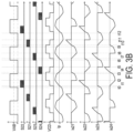
- FIG. 3 A is a schematic oscillogram showing the key waveforms of the three-level rectification DC/DC converter of FIG. 1 while applying positive sequence control to the secondary switches;
- FIG. 3 B is a schematic oscillogram showing the key waveforms of the three-level rectification DC/DC converter of FIG. 1 while applying negative sequence control to the secondary switches;
- FIGS. 4 A to 4 L show the working state of the three-level rectification DC/DC converter of FIG. 1 in one period while applying the positive sequence control to the secondary switches;
- FIG. 5 A shows an equivalent circuit of the three-level rectification DC/DC converter of FIG. 1 while the first voltage is at a high level and the secondary switches being turned on positively;
- FIG. 5 B shows an equivalent circuit of the three-level rectification DC/DC converter of FIG. 1 while the first voltage is at a low level and the secondary switches being turned on positively;
- FIG. 6 A is a schematic oscillogram showing the key waveforms of the three-level rectification DC/DC converter of FIG. 1 while applying the positive sequence control and partial synchronous rectification to the secondary switches;
- FIG. 6 B is a schematic oscillogram showing the key waveforms of the three-level rectification DC/DC converter of FIG. 1 while applying the negative sequence control and partial synchronous rectification to the secondary switches;
- FIG. 7 A is a schematic oscillogram showing the key waveforms of the three-level rectification DC/DC converter of FIG. 1 while applying the positive sequence control and complete synchronous rectification to the secondary switches;
- FIG. 7 B is a schematic oscillogram showing the key waveforms of the three-level rectification DC/DC converter of FIG. 1 while applying the negative sequence control and complete synchronous rectification to the secondary switches;
- FIG. 8 A is a schematic block diagram illustrating the variable frequency control applied to the three-level rectification DC/DC converter of FIG. 1 ;
- FIG. 8 B is a schematic block diagram illustrating the fixed-frequency control applied to the three-level rectification DC/DC converter of FIG. 1 ;
- FIG. 9 schematically shows a specific implementation of the resonant tank circuit of FIG. 1 ;
- FIG. 10 schematically shows a specific implementation of the primary circuit of FIG. 1 ;
- FIG. 11 A and FIG. 11 B are schematic oscillograms showing the key waveforms of the three-level rectification DC/DC converter of FIG. 10 while applying the positive sequence control and the negative sequence control to the secondary switches respectively;
- FIG. 12 A is a schematic oscillogram showing the key waveforms of the three-level rectification DC/DC converter of FIG. 10 while applying the positive sequence control and partial synchronous rectification to the secondary switches;
- FIG. 12 B is a schematic oscillogram showing the key waveforms of the three-level rectification DC/DC converter of FIG. 10 while applying the negative sequence control and partial synchronous rectification to the secondary switches;
- FIG. 13 A is a schematic oscillogram showing the key waveforms of the three-level rectification DC/DC converter of FIG. 10 while applying the positive sequence control and complete synchronous rectification to the secondary switches;
- FIG. 13 B is a schematic oscillogram showing the key waveforms of the three-level rectification DC/DC converter of FIG. 10 while applying the negative sequence control and complete synchronous rectification to the secondary switches;
- FIG. 14 schematically shows another specific implementation of the primary circuit of FIG. 1 ;
- FIG. 15 A and FIG. 15 B are schematic oscillograms showing the key waveforms of the three-level rectification DC/DC converter of FIG. 14 while applying the positive sequence control and the negative sequence control to the secondary switches respectively;
- FIG. 16 A is a schematic oscillogram showing the key waveforms of the three-level rectification DC/DC converter of FIG. 14 while applying the positive sequence control and partial synchronous rectification to the secondary switches;
- FIG. 16 B is a schematic oscillogram showing the key waveforms of the three-level rectification DC/DC converter of FIG. 14 while applying the negative sequence control and partial synchronous rectification to the secondary switches;
- FIG. 17 A is a schematic oscillogram showing the key waveforms of the three-level rectification DC/DC converter of FIG. 14 while applying the positive sequence control and complete synchronous rectification to the secondary switches;
- FIG. 17 B is a schematic oscillogram showing the key waveforms of the three-level rectification DC/DC converter of FIG. 14 while applying the negative sequence control and complete synchronous rectification to the secondary switches.
- FIG. 1 is a schematic circuit diagram illustrating a three-level rectification DC/DC converter according to an embodiment of the present disclosure
- FIG. 2 schematically shows an equivalent circuit of the three-level rectification DC/DC converter of FIG. 1
- the three-level rectification DC/DC converter 1 includes a primary circuit 11 , a resonant tank circuit 12 , and a secondary circuit 13 .
- the three-level rectification DC/DC converter 1 has the characteristic of a resonant circuit and can meet the bidirectional work requirement.
- the primary circuit 11 receives an input voltage Vin and includes a plurality of primary switches, and the primary circuit 11 is configured to provide a first voltage VAB. It is noted that the primary circuit 11 is represented by a voltage source which provides the first voltage VAB in this embodiment since the actual implementation of the primary circuit 11 is not limited. The specific implementation of the primary circuit 11 would be exemplified in the following descriptions.
- the resonant tank circuit 12 includes a resonant inductor Lr, a resonant capacitor Cr, and a transformer Tr.
- a first primary terminal 121 and a second primary terminal 122 of the resonant tank circuit 12 are coupled to the primary circuit 11 .
- a primary winding Np of the transformer Tr is coupled between the first primary terminal 121 and the second primary terminal 122 .
- a secondary winding Ns of the transformer Tr is coupled between a first secondary terminal 123 and a second secondary terminal 124 of the resonant tank circuit 12 .
- the voltage between the first primary terminal 121 and the second primary terminal 122 is the first voltage VAB
- the voltage between the first secondary terminal 123 and the second secondary terminal 124 is a second voltage VCD.
- Ip is the primary current
- Is is the secondary current.
- the secondary circuit 13 includes a switch bridge arm and a capacitor bridge arm.
- the switch bridge arm includes a first secondary switch S 21 , a second secondary switch S 22 , a third secondary switch S 23 , and a fourth secondary switch S 24 sequentially connected in series.
- a node C between the first secondary switch S 21 and the second secondary switch S 22 is connected to the first secondary terminal 123
- a node D between the third secondary switch S 23 and the fourth secondary switch S 24 is connected to the second secondary terminal 124 .
- the capacitor bridge arm includes a first output capacitor Co 1 and a second output capacitor Co 2 connected in series. A node between the first output capacitor Co 1 and the second output capacitor Co 2 is connected to a node between the second secondary switch S 22 and the third secondary switch S 23 .
- Two terminals of the capacitor bridge arm are connected to two terminals of the switch bridge arm respectively, and the voltage between the two terminals of the capacitor bridge arm is an output voltage Vo.
- FIG. 3 A is a schematic oscillogram showing the key waveforms of the three-level rectification DC/DC converter of FIG. 1 while applying positive sequence control to the secondary switches.
- FIG. 3 B is a schematic oscillogram showing the key waveforms of the three-level rectification DC/DC converter of FIG. 1 while applying negative sequence control to the secondary switches.
- S 21 , S 22 , S 23 , and S 24 represent the driving signals of the first secondary switch S 21 , the second secondary switch S 22 , the third secondary switch S 23 , and the fourth secondary switch S 24 respectively; and is 21 , is 22 , is 23 , and is 24 represent the currents flowing through the first secondary switch S 21 , the second secondary switch S 22 , the third secondary switch S 23 , and the fourth secondary switch S 24 respectively.
- FIG. 3 A and FIG. 3 B in any two consecutive periods of the first voltage VAB, there are two rising edges and two falling edges.
- the first secondary switch S 21 and the fourth secondary switch S 24 are in an on state for a preset time length after the two falling edges respectively.
- the second secondary switch S 22 and the third secondary switch S 23 are in an on state for the preset time length after the two rising edges respectively.
- the first secondary switch S 21 , the second secondary switch S 22 , the third secondary switch S 23 , and the fourth secondary switch S 24 have the same switching frequency equal to half of the frequency of the first voltage VAB. Further, all the secondary switches in secondary circuit 13 can be turned on with zero voltage switching.
- the said preset time length is obtained based on the input voltage Vin and the output voltage Vo. By controlling the preset time length, the duty ratio of each secondary switch can be adjusted, and the gain of the output voltage Vo can be controlled.
- the first voltage VAB is a square wave which is at a high level in one-half period and at a low level in the other half period, where the high level and the low level may be equal to +VAB/2 and ⁇ VAB/2 respectively, or equal to +VAB and 0 respectively.
- the difference between the oscillograms of FIG. 3 A and FIG. 3 B is that the control applied to the secondary switches is a positive sequence control or a negative sequence control.
- the phases of the second secondary switch S 22 , the first secondary switch S 21 , the third secondary switch S 23 , and the fourth secondary switch S 24 are sequentially out of phase by 90 degrees.
- a first rising edge, a first falling edge, a second rising edge, and a second falling edge occur sequentially.
- the first secondary switch S 21 and the fourth secondary switch S 24 are in the on state for the preset time length after the first falling edge and the second falling edge respectively.
- the second secondary switch S 22 and the third secondary switch S 23 are in the on state for the preset time length after the first rising edge and the second rising edge respectively.
- the phases of the fourth secondary switch S 24 , the third secondary switch S 23 , the first secondary switch S 21 , and the second secondary switch S 22 are sequentially out of phase by 90 degrees.
- a first rising edge, a first falling edge, a second rising edge, and a second falling edge occur sequentially.
- the first secondary switch S 21 and the fourth secondary switch S 24 are in the on state for the preset time length after the second falling edge and the first falling edge respectively.
- the second secondary switch S 22 and the third secondary switch S 23 are in the on state for the preset time length after the first rising edge and the second rising edge respectively.
- FIG. 3 A and FIG. 3 B the duration from time t 0 to t 12 is regarded as one period of the secondary switches.
- FIGS. 4 A to 4 L show the working state of the three-level rectification DC/DC converter of FIG. 1 in one period while applying the positive sequence control to the secondary switches. In specific, FIGS. 4 A to 4 L show the switching state and the current flowing direction of the three-level rectification DC/DC converter 1 within one period.
- FIGS. 4 B, 4 E, 4 H, and 4 K show the corresponding working states of the three-level rectification DC/DC converter 1 .
- the equivalent circuit of the three-level rectification DC/DC converter 1 during the duration from time t 1 to t 2 and the duration from time t 7 to t 8 is shown in FIG. 5 A .
- the equivalent circuit of the three-level rectification DC/DC converter 1 during the duration from time t 4 to t 5 and the duration from time t 10 to t 11 is shown in FIG. 5 B . From FIGS.
- the energy is stored in the resonant inductor Lr during the operating process, thereby achieving the high-gain voltage output.
- the four secondary switches since the four secondary switches are turned on by turns, the four secondary switches have the same effective current and conduction loss naturally, which makes the heat dissipation design and selection for switch components much easier.
- the secondary switches may be controlled with synchronous rectification. Namely, the secondary switch is driven during the current flowing reversely therethrough, thereby reducing the conduction loss of the secondary switches.
- FIG. 6 A is a schematic oscillogram showing the key waveforms of the three-level rectification DC/DC converter of FIG. 1 while applying the positive sequence control and partial synchronous rectification to the secondary switches.
- FIG. 6 B is a schematic oscillogram showing the key waveforms of the three-level rectification DC/DC converter of FIG. 1 while applying the negative sequence control and partial synchronous rectification to the secondary switches. As shown in FIG. 6 A and FIG. 6 B , while applying the partial synchronous rectification, in addition to the time durations of being in the on state shown in FIG. 3 A and FIG.
- the first secondary switch S 21 , the second secondary switch S 22 , the third secondary switch S 23 , and the fourth secondary switch S 24 are further in the on state during a partial duration within a duration of the currents flowing reversely through the first secondary switch S 21 , the second secondary switch S 22 , the third secondary switch S 23 , and the fourth secondary switch S 24 respectively.
- the first secondary switch S 21 , the second secondary switch S 22 , the third secondary switch S 23 , and the fourth secondary switch S 24 have the same duty ratio of 25% and still maintain a phase difference of 90 degrees, and the switching frequency thereof is still equal to a half of the frequency of the first voltage VAB.
- FIG. 7 A is a schematic oscillogram showing the key waveforms of the three-level rectification DC/DC converter of FIG. 1 while applying the positive sequence control and complete synchronous rectification to the secondary switches.
- FIG. 7 B is a schematic oscillogram showing the key waveforms of the three-level rectification DC/DC converter of FIG. 1 while applying the negative sequence control and complete synchronous rectification to the secondary switches. As shown in FIG. 7 A and FIG. 7 B , while applying the complete synchronous rectification, in addition to the durations of being in the on state shown in FIG. 3 A and FIG.
- the first secondary switch S 21 , the second secondary switch S 22 , the third secondary switch S 23 , and the fourth secondary switch S 24 are further in the on state during all durations within the duration of the currents flowing reversely through the first secondary switch S 21 , the second secondary switch S 22 , the third secondary switch S 23 , and the fourth secondary switch S 24 respectively.
- the driving signals of the first secondary switch S 21 and the second secondary switch S 22 are complementary
- the driving signals of the third secondary switch S 23 and the fourth secondary switch S 24 are complementary.
- control for the three-level rectification DC/DC converter 1 of the present disclosure may be divided into a variable frequency control and a fixed-frequency control.
- FIG. 8 A is a schematic block diagram illustrating the variable frequency control applied to the three-level rectification DC/DC converter of FIG. 1 . While applying the variable frequency control, as shown in FIG. 8 A , the three-level rectification DC/DC converter 1 further includes a control module 14 a .
- the control module 14 a is configured to acquire an input voltage signal Vin_FB, an output voltage signal Vo_FB and an output current signal Io_FB reflecting the input voltage Vin, the output voltage Vo and the output current Io respectively through detection, and to control the operation of all the primary and secondary switches.
- the control module 14 a includes a regulator 141 , and the regulator 141 generates a regulating signal according to the output voltage signal Vo_FB, the output current signal Io_FB, an output reference voltage Vo_ref and an output reference current Io_ref.
- the control module 14 a further includes a voltage-controlled oscillator 142 and a controller 143 .
- the voltage-controlled oscillator 142 is coupled to the regulator 141 and generates a switching frequency fs of all the primary switches according to the regulating signal.
- the controller 143 is coupled to the voltage-controlled oscillator 142 , and generates an on-time Ton of all the secondary switches according to the input voltage signal Vin_FB, the output voltage signal Vo_FB and the switching frequency fs of all the primary switches.
- the turns ratio n of the transformer Tr is fixed, the relations among the on-time Ton of all the secondary switches, the input voltage Vin, the output voltage Vo and the switching frequency fs of all the primary switches are conformed with the curve shown in FIG. 8 A .
- the on-time Ton of the secondary switches may be obtained through calculation or look-up table.
- FIG. 8 B is a schematic block diagram illustrating the fixed-frequency control applied to the three-level rectification DC/DC converter of FIG. 1 . While applying the fixed-frequency control, the switching frequency fs of all the primary switches is fixed and is larger than the resonant frequency of the resonant tank circuit 12 . As shown in FIG. 8 B , the three-level rectification DC/DC converter 1 further includes a control module 14 b .
- the control module 14 b is configured to acquire an input voltage signal Vin_FB, an output voltage signal Vo_FB and an output current signal Io_FB reflecting the input voltage Vin, the output voltage Vo and the output current Io respectively through detection, and to control the operation of all the primary and secondary switches.
- the control module 14 b includes a regulator 141 , and the regulator 141 generates a regulating signal according to the output voltage signal Vo_FB, the output current signal Io_FB, an output reference voltage Vo_ref, and an output reference current Io_ref.
- the control module 14 b further includes a PWM controller 144 .
- the PWM controller 144 is coupled to the regulator 141 and generates the driving signals of all the primary and secondary switches according to the regulating signal.
- FIG. 9 schematically shows a specific implementation of the resonant tank circuit 12 .
- the resonant inductor Lr, the primary winding Np, and the resonant capacitor Cr are sequentially connected between the first primary terminal 121 and the second primary terminal 122 in series, but not limited thereto.
- the resonant capacitor Cr may be connected in series between the secondary winding Ns and the second secondary terminal 124
- the resonant inductor Lr may be connected in series between the secondary winding Ns and the first secondary terminal 123 .
- the resonant inductor Lr includes a primary resonant inductor Lrp and a secondary resonant inductor Lrs, the primary resonant inductor Lrp is connected in series between the primary winding Np and the first primary terminal 121 , and the secondary resonant inductor Lrs is connected in series between the secondary winding Ns and the first secondary terminal 123 .
- the resonant capacitor Cr includes a primary resonant capacitor Crp and a secondary resonant capacitor Crs, the primary resonant capacitor Crp is connected in series between the primary winding Np and the second primary terminal 122 , and the secondary resonant capacitor Crs is connected in series between the secondary winding Ns and the second secondary terminal 124 .
- the actual circuit topology of the primary circuit is not limited, and the primary circuit is for example but not limited to a full-bridge circuit, a half-bridge circuit, a serial-half-bridge circuit, a three-level circuit with a flying capacitor, or a three-level circuit with the clamped midpoint.
- Two kinds of actual circuit topologies of the primary circuit are exemplified as follows.
- the primary circuit 11 a is a full-bridge circuit, and the primary circuit 11 a includes an input capacitor Cin, a first bridge arm, and a second bridge arm connected to each other in parallel.
- the voltage on the input capacitor Cin is the input voltage Vin.
- the first bridge arm includes a first primary switch S 11 and a second primary switch S 12 connected in series, and a node B between the first primary switch S 11 and the second primary switch S 12 is connected to the second primary terminal 122 .
- the second bridge arm includes a third primary switch S 13 and a fourth primary switch S 14 , and a node A between the third primary switch S 13 and the fourth primary switch S 14 is connected to the first primary terminal 121 .
- FIG. 11 A and FIG. 11 B are schematic oscillograms showing the key waveforms of the three-level rectification DC/DC converter of FIG. 10 while applying the positive sequence control and the negative sequence control to the secondary switches respectively.
- FIG. 12 A is a schematic oscillogram showing the key waveforms of the three-level rectification DC/DC converter of FIG. 10 while applying the positive sequence control and partial synchronous rectification to the secondary switches.
- FIG. 12 B is a schematic oscillogram showing the key waveforms of the three-level rectification DC/DC converter of FIG. 10 while applying the negative sequence control and partial synchronous rectification to the secondary switches.
- FIG. 11 A and FIG. 11 B are schematic oscillograms showing the key waveforms of the three-level rectification DC/DC converter of FIG. 10 while applying the positive sequence control and partial synchronous rectification to the secondary switches respectively.
- FIG. 12 A is a schematic oscillogram showing the key waveforms of the three-level rectification DC/DC converter of FIG. 10 while
- FIG. 13 A is a schematic oscillogram showing the key waveforms of the three-level rectification DC/DC converter of FIG. 10 while applying the positive sequence control and complete synchronous rectification to the secondary switches.
- FIG. 13 B is a schematic oscillogram showing the key waveforms of the three-level rectification DC/DC converter of FIG. 10 while applying the negative sequence control and complete synchronous rectification to the secondary switches.
- the primary circuit 11 b is a serial-half-bridge circuit, and the primary circuit 11 b includes a first bridge arm and a second bridge arm.
- the voltage between the two terminals of the first bridge arm is the input voltage Vin, and the two terminals of the first bridge arm are connected to two terminals of the second bridge arm respectively.
- the first bridge arm includes a first input capacitor C 1 and a second input capacitor C 2 connected in series.
- the second bridge arm includes a first primary switch S 11 , a second primary switch S 12 , a third primary switch S 13 , and a fourth primary switch S 14 sequentially connected in series.
- a node A between the first primary switch S 11 and the second primary switch S 12 is connected to the first primary terminal 121 .
- FIG. 15 A and FIG. 15 B are schematic oscillograms showing the key waveforms of the three-level rectification DC/DC converter of FIG. 14 while applying the positive sequence control and the negative sequence control to the secondary switches respectively.
- FIG. 16 A is a schematic oscillogram showing the key waveforms of the three-level rectification DC/DC converter of FIG.
- FIG. 16 B is a schematic oscillogram showing the key waveforms of the three-level rectification DC/DC converter of FIG. 14 while applying the negative sequence control and partial synchronous rectification to the secondary switches.
- FIG. 17 A is a schematic oscillogram showing the key waveforms of the three-level rectification DC/DC converter of FIG. 14 while applying the positive sequence control and complete synchronous rectification to the secondary switches.
- FIG. 17 B is a schematic oscillogram showing the key waveforms of the three-level rectification DC/DC converter of FIG. 14 while applying the negative sequence control and complete synchronous rectification to the secondary switches.
- the present disclosure provides a three-level rectification DC/DC converter which has the characteristic of a resonant circuit and can meet the bidirectional work requirement.
- the three-level rectification DC/DC converter has the characteristic of storing energy through short-circuiting the secondary circuit thereof, thereby achieving the output with high voltage gain. Since the highest voltage on the secondary switch equals one-half of the output voltage, the secondary switch can be implemented by switch components with low withstand voltage, which makes the selection for switch components easier and reduces the cost.
- the energy is stored in the resonant inductor during the operating process by the secondary circuit equivalent to be short-circuited, thereby achieving the high-gain voltage output.
- the four secondary switches are turned on by turns, the four secondary switches have the same effective current and conduction loss naturally, which makes the heat dissipation design and selection for switch components much easier.
Abstract
The present disclosure provides a three-level rectification DC/DC converter including primary and secondary circuits and a resonant tank circuit. A voltage between two primary terminals is a first voltage. The secondary circuit includes a switch bridge arm and a capacitor bridge arm. The switch bridge arm includes four switches serially connected. A node between the first and second switches is connected to the first secondary terminal, a node between the third and fourth switches is connected to the second secondary terminal, and a node between the second and third switches is connected between two capacitors of the capacitor bridge arm. In two consecutive periods of the first voltage, the first and fourth switches are in an on state for a preset time length after two falling edges respectively, and the second and third switches are in the on state for the preset time length after two rising edges respectively.
Description
This application claims priority to China Patent Application No. 202111463253.9, filed on Dec. 2, 2021, the entire contents of which are incorporated herein by reference for all purposes.
The present disclosure relates to a DC/DC converter, and more particularly to a three-level rectification DC/DC converter.
Low-voltage DC/DC converter, bidirectional OBC (on-board charger), and traction inverter are three main power conversion units. The OBC works as an energy conversion unit between AC power and DC power to supply power for power battery, and thus the OBC is necessary in the configuration of the electric vehicle. Recently, as the endurance of the electric vehicle keeps increasing, the battery voltage is changing from the conventional battery voltage of 400V to 800V, and the charging for the OBC is changing from single-phase charging to three-phase charging. Accordingly, the rectification voltage from AC power to DC power would reach 800V. Therefore, the primary and secondary circuits of the DC/DC converter would both relate to the applications with 800V.
As the conventional component with the withstand voltage of 650V can't be used, the SiC component with the withstand voltage of 1200 may be used instead. However, the cost is higher, and the high dv/dt caused by the SiC component may lead to EMI (electromagnetic interference) problem. In addition, although the wide-bandgap semiconductor device (GaN) is regarded as the development trend of power devices in the future, it is hard to be directly applied in the high-voltage (800V) work environment due to its limited withstand voltage. The multi-level technique can be utilized to overcome the said limitation, to expand the development and application of actual products.
With regard to applications with wide output voltage range in actual engineering, to meet the needs of high efficiency and high output voltage gain, the PWM (pulse width modulation) control with fixed frequency based on dual-active-bridge circuit and the resonant soft-switching control with variable frequency based on LLC circuit are usually used.
For the dual-active-bridge circuit, the multiple phase shift technique is taken to realize the zero-voltage switching of switches under the wide output range condition. However, the control therefor is relatively complicated, and the high turn-off current may cause high turn-off stress and EMI problem.
For the LLC circuit, the variable frequency control is taken to allow all the switches to achieve zero voltage switching, and it is relatively easy to implement the variable frequency control. However, the LLC is unable to meet the bidirectional work requirement in actual applications.
Therefore, there is a need of providing a three-level rectification DC/DC converter to overcome the drawbacks of conventional technologies.
The present disclosure provides a three-level rectification DC/DC converter which has the characteristic of a resonant circuit and can meet the bidirectional work requirement. In addition, the three-level rectification DC/DC converter has the characteristic of storing energy through short-circuiting the secondary circuit thereof, thereby achieving the output with high voltage gain.
In accordance with an aspect of the present disclosure, a three-level rectification DC/DC converter is provided. The three-level rectification DC/DC converter includes a primary circuit, a resonant tank circuit, and a secondary circuit. The primary circuit receives an input voltage and includes a plurality of primary switches. The resonant tank circuit includes a resonant inductor, a resonant capacitor, and a transformer. A first primary terminal and a second primary terminal of the resonant tank circuit are coupled to the primary circuit. A primary winding of the transformer is coupled between the first and second primary terminals. A secondary winding of the transformer is coupled between a first secondary terminal and a second secondary terminal of the resonant tank circuit. A voltage between the first and second primary terminals is a first voltage, and a voltage between the first and second secondary terminals is a second voltage. The secondary circuit includes a switch bridge arm and a capacitor bridge arm. The switch bridge arm includes a first secondary switch, a second secondary switch, a third secondary switch, and a fourth secondary switch sequentially connected in series. A node between the first and second secondary switches is connected to the first secondary terminal, and a node between the third and fourth secondary switches is connected to the second secondary terminal. The capacitor bridge arm includes a first output capacitor and a second output capacitor connected in series. A node between the first and second output capacitors is connected to a node between the second and third secondary switches. Two terminals of the capacitor bridge arm are connected to two terminals of the switch bridge arm, and a voltage between the two terminals of the capacitor bridge arm is an output voltage. The first, second, third, and fourth secondary switches have a same switching frequency. There are two rising edges and two falling edges in two consecutive periods of the first voltage, the first and fourth secondary switches are at least in an on state for a preset time length after the two falling edges respectively, and the second and third secondary switches are at least in the on state for the preset time length after the two rising edges respectively.
The present disclosure will now be described more specifically regarding the following embodiments. It is to be noted that the following descriptions of preferred embodiments of this disclosure are presented herein for purpose of illustration and description only. It is not intended to be exhaustive or to be limited to the precise form disclosed.
The primary circuit 11 receives an input voltage Vin and includes a plurality of primary switches, and the primary circuit 11 is configured to provide a first voltage VAB. It is noted that the primary circuit 11 is represented by a voltage source which provides the first voltage VAB in this embodiment since the actual implementation of the primary circuit 11 is not limited. The specific implementation of the primary circuit 11 would be exemplified in the following descriptions.
The resonant tank circuit 12 includes a resonant inductor Lr, a resonant capacitor Cr, and a transformer Tr. A first primary terminal 121 and a second primary terminal 122 of the resonant tank circuit 12 are coupled to the primary circuit 11. A primary winding Np of the transformer Tr is coupled between the first primary terminal 121 and the second primary terminal 122. A secondary winding Ns of the transformer Tr is coupled between a first secondary terminal 123 and a second secondary terminal 124 of the resonant tank circuit 12. The voltage between the first primary terminal 121 and the second primary terminal 122 is the first voltage VAB, and the voltage between the first secondary terminal 123 and the second secondary terminal 124 is a second voltage VCD. In FIG. 1 and FIG. 2 , Ip is the primary current, and Is is the secondary current.
The secondary circuit 13 includes a switch bridge arm and a capacitor bridge arm. The switch bridge arm includes a first secondary switch S21, a second secondary switch S22, a third secondary switch S23, and a fourth secondary switch S24 sequentially connected in series. A node C between the first secondary switch S21 and the second secondary switch S22 is connected to the first secondary terminal 123, and a node D between the third secondary switch S23 and the fourth secondary switch S24 is connected to the second secondary terminal 124. The capacitor bridge arm includes a first output capacitor Co1 and a second output capacitor Co2 connected in series. A node between the first output capacitor Co1 and the second output capacitor Co2 is connected to a node between the second secondary switch S22 and the third secondary switch S23. Two terminals of the capacitor bridge arm are connected to two terminals of the switch bridge arm respectively, and the voltage between the two terminals of the capacitor bridge arm is an output voltage Vo.
The difference between the oscillograms of FIG. 3A and FIG. 3B is that the control applied to the secondary switches is a positive sequence control or a negative sequence control.
When the positive sequence control is applied to the secondary switches, the phases of the second secondary switch S22, the first secondary switch S21, the third secondary switch S23, and the fourth secondary switch S24 are sequentially out of phase by 90 degrees. As shown in FIG. 3A , in two consecutive periods of the first voltage VAB (e.g., the duration from time t0 to t12), a first rising edge, a first falling edge, a second rising edge, and a second falling edge occur sequentially. The first secondary switch S21 and the fourth secondary switch S24 are in the on state for the preset time length after the first falling edge and the second falling edge respectively. The second secondary switch S22 and the third secondary switch S23 are in the on state for the preset time length after the first rising edge and the second rising edge respectively.
When the negative sequence control is applied to the secondary switches, the phases of the fourth secondary switch S24, the third secondary switch S23, the first secondary switch S21, and the second secondary switch S22 are sequentially out of phase by 90 degrees. As shown in FIG. 3B , in two consecutive periods of the first voltage VAB (e.g., the duration from time t0 to t12), a first rising edge, a first falling edge, a second rising edge, and a second falling edge occur sequentially. The first secondary switch S21 and the fourth secondary switch S24 are in the on state for the preset time length after the second falling edge and the first falling edge respectively. The second secondary switch S22 and the third secondary switch S23 are in the on state for the preset time length after the first rising edge and the second rising edge respectively.
In FIG. 3A and FIG. 3B , the duration from time t0 to t12 is regarded as one period of the secondary switches. FIGS. 4A to 4L show the working state of the three-level rectification DC/DC converter of FIG. 1 in one period while applying the positive sequence control to the secondary switches. In specific, FIGS. 4A to 4L show the switching state and the current flowing direction of the three-level rectification DC/DC converter 1 within one period. The duration from time t1 to t2 (FIG. 4B ), the duration from time t4 to t5 (FIG. 4E ), the duration from time t7 to t8 (FIG. 4H ), and the duration from time t10 to t11 (FIG. 4K ) respectively correspond to the durations of the second secondary switch S22, the first secondary switch S21, the third secondary switch S23, and the fourth secondary switch S24 being turned on positively. FIGS. 4B, 4E, 4H, and 4K show the corresponding working states of the three-level rectification DC/DC converter 1. The equivalent circuit of the three-level rectification DC/DC converter 1 during the duration from time t1 to t2 and the duration from time t7 to t8 is shown in FIG. 5A . The equivalent circuit of the three-level rectification DC/DC converter 1 during the duration from time t4 to t5 and the duration from time t10 to t11 is shown in FIG. 5B . From FIGS. 4B, 4E, 4H, 4K, 5A, and 5B , it can be seen that the capacitor voltage is always equal to Vo/2n (n=Ns/Np) when the secondary switches are turned on positively, which can be regarded as a constant voltage source. Accordingly, the secondary circuit 13 is equivalent to be in a short-circuit state. At this time, the energy is stored in the resonant inductor Lr through the first voltage VAB, which prepares for the high-gain energy output in the next duration.
Correspondingly, while applying the negative sequence control to the secondary switches, the working state of the three-level rectification DC/DC converter of FIG. 1 in one period can be derived from FIGS. 4A to 4L , and thus the detailed descriptions thereof are omitted herein.
From the above descriptions, in the three-level rectification DC/DC converter 1 of the present disclosure, through controlling the four secondary switches in the period, the energy is stored in the resonant inductor Lr during the operating process, thereby achieving the high-gain voltage output. Moreover, since the four secondary switches are turned on by turns, the four secondary switches have the same effective current and conduction loss naturally, which makes the heat dissipation design and selection for switch components much easier.
In an embodiment, to further improve the work efficiency of the three-level rectification DC/DC converter 1, the secondary switches may be controlled with synchronous rectification. Namely, the secondary switch is driven during the current flowing reversely therethrough, thereby reducing the conduction loss of the secondary switches.
In addition, depending on whether the switching frequency of primary switches is variable, the control for the three-level rectification DC/DC converter 1 of the present disclosure may be divided into a variable frequency control and a fixed-frequency control.
In addition, in the three-level rectification DC/DC converter 1 of the present disclosure, the resonant inductor Lr and the resonant capacitor Cr of the resonant tank circuit 12 have various kinds of actual implementations. FIG. 9 schematically shows a specific implementation of the resonant tank circuit 12. In the embodiment shown in FIG. 9 , the resonant inductor Lr, the primary winding Np, and the resonant capacitor Cr are sequentially connected between the first primary terminal 121 and the second primary terminal 122 in series, but not limited thereto. For example, the resonant capacitor Cr may be connected in series between the secondary winding Ns and the second secondary terminal 124, and the resonant inductor Lr may be connected in series between the secondary winding Ns and the first secondary terminal 123. Further, as exemplified in FIG. 10 , in an embodiment, the resonant inductor Lr includes a primary resonant inductor Lrp and a secondary resonant inductor Lrs, the primary resonant inductor Lrp is connected in series between the primary winding Np and the first primary terminal 121, and the secondary resonant inductor Lrs is connected in series between the secondary winding Ns and the first secondary terminal 123. In an embodiment, the resonant capacitor Cr includes a primary resonant capacitor Crp and a secondary resonant capacitor Crs, the primary resonant capacitor Crp is connected in series between the primary winding Np and the second primary terminal 122, and the secondary resonant capacitor Crs is connected in series between the secondary winding Ns and the second secondary terminal 124.
Moreover, in the three-level rectification DC/DC converter 1 of the present disclosure, the actual circuit topology of the primary circuit is not limited, and the primary circuit is for example but not limited to a full-bridge circuit, a half-bridge circuit, a serial-half-bridge circuit, a three-level circuit with a flying capacitor, or a three-level circuit with the clamped midpoint. Two kinds of actual circuit topologies of the primary circuit are exemplified as follows.
In an embodiment, as shown in FIG. 10 , the primary circuit 11 a is a full-bridge circuit, and the primary circuit 11 a includes an input capacitor Cin, a first bridge arm, and a second bridge arm connected to each other in parallel. The voltage on the input capacitor Cin is the input voltage Vin. The first bridge arm includes a first primary switch S11 and a second primary switch S12 connected in series, and a node B between the first primary switch S11 and the second primary switch S12 is connected to the second primary terminal 122. The second bridge arm includes a third primary switch S13 and a fourth primary switch S14, and a node A between the third primary switch S13 and the fourth primary switch S14 is connected to the first primary terminal 121. All the primary switches in the primary circuit 11 a can be turned on with zero voltage switching. FIG. 11A and FIG. 11B are schematic oscillograms showing the key waveforms of the three-level rectification DC/DC converter of FIG. 10 while applying the positive sequence control and the negative sequence control to the secondary switches respectively. FIG. 12A is a schematic oscillogram showing the key waveforms of the three-level rectification DC/DC converter of FIG. 10 while applying the positive sequence control and partial synchronous rectification to the secondary switches. FIG. 12B is a schematic oscillogram showing the key waveforms of the three-level rectification DC/DC converter of FIG. 10 while applying the negative sequence control and partial synchronous rectification to the secondary switches. FIG. 13A is a schematic oscillogram showing the key waveforms of the three-level rectification DC/DC converter of FIG. 10 while applying the positive sequence control and complete synchronous rectification to the secondary switches. FIG. 13B is a schematic oscillogram showing the key waveforms of the three-level rectification DC/DC converter of FIG. 10 while applying the negative sequence control and complete synchronous rectification to the secondary switches.
In an embodiment, as shown in FIG. 14 , the primary circuit 11 b is a serial-half-bridge circuit, and the primary circuit 11 b includes a first bridge arm and a second bridge arm. The voltage between the two terminals of the first bridge arm is the input voltage Vin, and the two terminals of the first bridge arm are connected to two terminals of the second bridge arm respectively. The first bridge arm includes a first input capacitor C1 and a second input capacitor C2 connected in series. The second bridge arm includes a first primary switch S11, a second primary switch S12, a third primary switch S13, and a fourth primary switch S14 sequentially connected in series. A node A between the first primary switch S11 and the second primary switch S12 is connected to the first primary terminal 121. A node between the second primary switch S12 and the third primary switch S13 is connected to a node between the first input capacitor C1 and the second input capacitor C2. A node B between the third primary switch S13 and the fourth primary switch S14 is connected to the second primary terminal 122. All the primary switches in the primary circuit 11 b can be turned on with zero voltage switching. FIG. 15A and FIG. 15B are schematic oscillograms showing the key waveforms of the three-level rectification DC/DC converter of FIG. 14 while applying the positive sequence control and the negative sequence control to the secondary switches respectively. FIG. 16A is a schematic oscillogram showing the key waveforms of the three-level rectification DC/DC converter of FIG. 14 while applying the positive sequence control and partial synchronous rectification to the secondary switches. FIG. 16B is a schematic oscillogram showing the key waveforms of the three-level rectification DC/DC converter of FIG. 14 while applying the negative sequence control and partial synchronous rectification to the secondary switches. FIG. 17A is a schematic oscillogram showing the key waveforms of the three-level rectification DC/DC converter of FIG. 14 while applying the positive sequence control and complete synchronous rectification to the secondary switches. FIG. 17B is a schematic oscillogram showing the key waveforms of the three-level rectification DC/DC converter of FIG. 14 while applying the negative sequence control and complete synchronous rectification to the secondary switches.
In summary, the present disclosure provides a three-level rectification DC/DC converter which has the characteristic of a resonant circuit and can meet the bidirectional work requirement. In addition, the three-level rectification DC/DC converter has the characteristic of storing energy through short-circuiting the secondary circuit thereof, thereby achieving the output with high voltage gain. Since the highest voltage on the secondary switch equals one-half of the output voltage, the secondary switch can be implemented by switch components with low withstand voltage, which makes the selection for switch components easier and reduces the cost. Moreover, through controlling the four secondary switches in the period, the energy is stored in the resonant inductor during the operating process by the secondary circuit equivalent to be short-circuited, thereby achieving the high-gain voltage output. Furthermore, since the four secondary switches are turned on by turns, the four secondary switches have the same effective current and conduction loss naturally, which makes the heat dissipation design and selection for switch components much easier.
While the disclosure has been described in terms of what is presently considered to be the most practical and preferred embodiments, it is to be understood that the disclosure needs not to be limited to the disclosed embodiment. On the contrary, it is intended to cover various modifications and similar arrangements included within the spirit and scope of the appended claims which are to be accorded with the broadest interpretation to encompass all such modifications and similar structures.
Claims (21)
1. A three-level rectification DC/DC converter, comprising:
a primary circuit receiving an input voltage and comprising a plurality of primary switches;
a resonant tank circuit comprising a resonant inductor, a resonant capacitor, and a transformer, wherein a first primary terminal and a second primary terminal of the resonant tank circuit are coupled to the primary circuit, a primary winding of the transformer is coupled between the first and second primary terminals, a secondary winding of the transformer is coupled between a first secondary terminal and a second secondary terminal of the resonant tank circuit, a voltage between the first and second primary terminals is a first voltage, a voltage between the first and second secondary terminals is a second voltage; and
a secondary circuit comprising a switch bridge arm and a capacitor bridge arm, wherein the switch bridge arm comprises a first secondary switch, a second secondary switch, a third secondary switch, and a fourth secondary switch sequentially connected in series, a node between the first and second secondary switches is connected to the first secondary terminal, a node between the third and fourth secondary switches is connected to the second secondary terminal, the capacitor bridge arm comprises a first output capacitor and a second output capacitor connected in series, a node between the first and second output capacitors is connected to a node between the second and third secondary switches, two terminals of the capacitor bridge arm are connected to two terminals of the switch bridge arm, and a voltage between the two terminals of the capacitor bridge arm is an output voltage,
wherein the first, second, third, and fourth secondary switches have a same switching frequency, there are two rising edges and two falling edges in two consecutive periods of the first voltage, the first and fourth secondary switches are at least in an on state for a preset time length after the two falling edges respectively, and the second and third secondary switches are at least in the on state for the preset time length after the two rising edges respectively.
2. The three-level rectification DC/DC converter according to claim 1 , wherein a first rising edge, a first falling edge, a second rising edge, and a second falling edge occur sequentially in the two consecutive periods of the first voltage, the first and fourth secondary switches are at least in the on state for the preset time length after the first and second falling edges respectively, and the second and third secondary switches are at least in the on state for the preset time length after the first and second rising edges respectively.
3. The three-level rectification DC/DC converter according to claim 2 , wherein phases of the second, first, third, and fourth secondary switches are sequentially out of phase by 90 degrees.
4. The three-level rectification DC/DC converter according to claim 2 , wherein the switching frequency of the first, second, third, and fourth secondary switches is equal to a half of a frequency of the first voltage.
5. The three-level rectification DC/DC converter according to claim 1 , wherein a first rising edge, a first falling edge, a second rising edge, and a second falling edge occur sequentially in the two consecutive periods of the first voltage, the first and fourth secondary switches are at least in the on state for the preset time length after the second and first falling edges respectively, and the second and third secondary switches are at least in the on state for the preset time length after the first and second rising edges respectively.
6. The three-level rectification DC/DC converter according to claim 5 , wherein phases of the fourth, third, first, and second secondary switches are sequentially out of phase by 90 degrees.
7. The three-level rectification DC/DC converter according to claim 5 , wherein the switching frequency of the first, second, third, and fourth secondary switches is equal to a half of a frequency of the first voltage.
8. The three-level rectification DC/DC converter according to claim 1 , wherein the first, second, third, and fourth secondary switches are further in the on state during a partial duration within a duration of currents flowing reversely through the first, second, third, and fourth secondary switches respectively.
9. The three-level rectification DC/DC converter according to claim 8 , wherein a duty ratio of the first, second, third, and fourth secondary switches are equal to 25%.
10. The three-level rectification DC/DC converter according to claim 1 , wherein the first, second, third, and fourth secondary switches are further in the on state during all durations within a duration of currents flowing reversely through the first, second, third, and fourth secondary switches respectively.
11. The three-level rectification DC/DC converter according to claim 10 , wherein driving signals of the first and second secondary switches are complementary, and driving signals of the third and fourth secondary switches are complementary.
12. The three-level rectification DC/DC converter according to claim 1 , wherein the preset time length is obtained based on the input voltage and the output voltage.
13. The three-level rectification DC/DC converter according to claim 1 , wherein all the primary and secondary switches are turned on with zero voltage switching.
14. The three-level rectification DC/DC converter according to claim 1 , wherein the first voltage is a square wave which is at a high level in one-half period and at a low level in the other half period.
15. The three-level rectification DC/DC converter according to claim 1 , wherein the primary circuit comprises an input capacitor, a first bridge arm, and a second bridge arm connected to each other in parallel, a voltage on the input capacitor is the input voltage, the first bridge arm comprises a first primary switch and a second primary switch connected in series, a node between the first and second primary switches is connected to the second primary terminal, the second bridge arm comprises a third primary switch and a fourth primary switch, and a node between the third and fourth primary switches is connected to the first primary terminal.
16. The three-level rectification DC/DC converter according to claim 1 , wherein the primary circuit comprises a first bridge arm and a second bridge arm, a voltage between two terminals of the first bridge arm is the input voltage, the two terminals of the first bridge arm are connected to two terminals of the second bridge arm respectively, the first bridge arm comprises a first input capacitor and a second input capacitor connected in series, the second bridge arm comprises a first primary switch, a second primary switch, a third primary switch and a fourth primary switch sequentially connected in series, a node between the first and second primary switches is connected to the first primary terminal, a node between the second and third primary switches is connected to a node between the first and second input capacitors, and a node between the third and fourth primary switches is connected to the second primary terminal.
17. The three-level rectification DC/DC converter according to claim 1 , wherein in the resonant tank circuit, the resonant inductor, the primary winding, and the resonant capacitor are connected in series between the first and second primary terminals.
18. The three-level rectification DC/DC converter according to claim 1 , further comprising a control module, wherein the control module is configured to acquire an input voltage signal, an output voltage signal, and an output current signal reflecting the input voltage, the output voltage, and an output current respectively through detection and to control the operation of all the primary and secondary switches, the control module comprises a regulator, and the regulator generates a regulating signal according to the output voltage signal, the output current signal, an output reference voltage, and an output reference current.
19. The three-level rectification DC/DC converter according to claim 18 , wherein the control module further comprises a voltage-controlled oscillator and a controller, the voltage-controlled oscillator is coupled to the regulator and generates a switching frequency of the plurality of primary switches according to the regulating signal, the controller is coupled to the voltage-controlled oscillator, and the controller generates an on-time of all the secondary switches according to the input voltage signal, the output voltage signal and the switching frequency of the plurality of primary switches.
20. The three-level rectification DC/DC converter according to claim 18 , wherein the control module further comprises a PWM controller coupled to the regulator, and the PWM controller generates driving signals of all the primary and secondary switches according to the regulating signal.
21. The three-level rectification DC/DC converter according to claim 20 , wherein a switching frequency of the plurality of primary switches is fixed and is larger than a resonant frequency of the resonant tank circuit.
Applications Claiming Priority (2)
| Application Number | Priority Date | Filing Date | Title |
|---|---|---|---|
| CN202111463253.9A CN114157157A (en) | 2021-12-02 | 2021-12-02 | Three-level rectification DC/DC converter |
| CN202111463253.9 | 2021-12-02 |
Publications (2)
| Publication Number | Publication Date |
|---|---|
| US20230179105A1 US20230179105A1 (en) | 2023-06-08 |
| US11750103B2 true US11750103B2 (en) | 2023-09-05 |
Family
ID=80456066
Family Applications (1)
| Application Number | Title | Priority Date | Filing Date |
|---|---|---|---|
| US17/573,970 Active 2042-04-03 US11750103B2 (en) | 2021-12-02 | 2022-01-12 | Three-level rectification dc/dc converter |
Country Status (3)
| Country | Link |
|---|---|
| US (1) | US11750103B2 (en) |
| EP (1) | EP4191861A1 (en) |
| CN (1) | CN114157157A (en) |
Families Citing this family (1)
| Publication number | Priority date | Publication date | Assignee | Title |
|---|---|---|---|---|
| CN116742956A (en) * | 2023-08-15 | 2023-09-12 | 深圳市高斯宝电气技术有限公司 | T-shaped three-level circuit |
Citations (16)
| Publication number | Priority date | Publication date | Assignee | Title |
|---|---|---|---|---|
| CN102624243A (en) | 2012-04-19 | 2012-08-01 | 中国矿业大学(北京) | Isolation-type half-bridge three-level dual-direction direct-current/direct-current (DC/DC) converter |
| US20180152097A1 (en) | 2016-11-29 | 2018-05-31 | Delta Electronics (Shanghai) Co.,Ltd. | Discharge control method for bus capacitor in power converter |
| US20180234022A1 (en) | 2015-08-26 | 2018-08-16 | Futurewei Technologies, Inc. | Ac/dc converters with wider voltage regulation range |
| US20180337610A1 (en) * | 2017-05-19 | 2018-11-22 | Infineon Technologies Austria Ag | PWM Controlled Resonant Converter |
| US20190068069A1 (en) * | 2017-08-31 | 2019-02-28 | Google Inc. | Programmable Power Adapter |
| CN109889049A (en) | 2019-03-08 | 2019-06-14 | 台达电子企业管理(上海)有限公司 | The control method and device of DC/DC converter |
| CN110048613A (en) | 2019-05-31 | 2019-07-23 | 芜湖康爱而电气有限公司 | A kind of three level DCDC translation circuit of bi-directional half bridge |
| CN111224553A (en) | 2020-03-09 | 2020-06-02 | 合肥博鳌电气科技有限公司 | Improved bidirectional half-bridge three-level LLC direct-current converter and synchronous control method thereof |
| US20200228017A1 (en) | 2019-01-16 | 2020-07-16 | Delta Electronics (Shanghai) Co., Ltd | Dc/dc converter and control method thereof |
| US20200228022A1 (en) * | 2019-01-16 | 2020-07-16 | Delta Electronics (Shanghai) Co., Ltd | Dc/dc converter and control method thereof |
| US20200266719A1 (en) * | 2019-02-15 | 2020-08-20 | Apple Inc. | Frequency Doubling Resonant Converter |
| US20210067045A1 (en) * | 2019-08-26 | 2021-03-04 | Delta Electronics, Inc. | Three-level modulation for wide output voltage range isolated dc/dc converters |
| CN213151913U (en) | 2020-07-30 | 2021-05-07 | 深圳市联明电源有限公司 | Output wide-range adjustable three-level soft switching change circuit |
| CN113037096A (en) | 2021-04-27 | 2021-06-25 | 燕山大学 | High-gain three-level current type bidirectional DC/DC converter and control method thereof |
| US20210226534A1 (en) | 2020-01-16 | 2021-07-22 | Delta Electronics (Shanghai) Co., Ltd. | Dc/dc converter and control method thereof |
| EP3916984A1 (en) | 2020-05-25 | 2021-12-01 | Delta Electronics, Inc. | Isolated dc/dc converters for wide output voltage range and control methods thereof |
-
2021
- 2021-12-02 CN CN202111463253.9A patent/CN114157157A/en active Pending
-
2022
- 2022-01-12 US US17/573,970 patent/US11750103B2/en active Active
- 2022-06-21 EP EP22180105.3A patent/EP4191861A1/en active Pending
Patent Citations (18)
| Publication number | Priority date | Publication date | Assignee | Title |
|---|---|---|---|---|
| CN102624243A (en) | 2012-04-19 | 2012-08-01 | 中国矿业大学(北京) | Isolation-type half-bridge three-level dual-direction direct-current/direct-current (DC/DC) converter |
| US20180234022A1 (en) | 2015-08-26 | 2018-08-16 | Futurewei Technologies, Inc. | Ac/dc converters with wider voltage regulation range |
| US20180152097A1 (en) | 2016-11-29 | 2018-05-31 | Delta Electronics (Shanghai) Co.,Ltd. | Discharge control method for bus capacitor in power converter |
| US20180337610A1 (en) * | 2017-05-19 | 2018-11-22 | Infineon Technologies Austria Ag | PWM Controlled Resonant Converter |
| US20190068069A1 (en) * | 2017-08-31 | 2019-02-28 | Google Inc. | Programmable Power Adapter |
| US20200228017A1 (en) | 2019-01-16 | 2020-07-16 | Delta Electronics (Shanghai) Co., Ltd | Dc/dc converter and control method thereof |
| US20200228022A1 (en) * | 2019-01-16 | 2020-07-16 | Delta Electronics (Shanghai) Co., Ltd | Dc/dc converter and control method thereof |
| US20200266719A1 (en) * | 2019-02-15 | 2020-08-20 | Apple Inc. | Frequency Doubling Resonant Converter |
| CN109889049A (en) | 2019-03-08 | 2019-06-14 | 台达电子企业管理(上海)有限公司 | The control method and device of DC/DC converter |
| US20200287466A1 (en) * | 2019-03-08 | 2020-09-10 | Delta Electronics (Shanghai) Co., Ltd. | Control method for dc/dc converter and dc/dc converter |
| CN110048613A (en) | 2019-05-31 | 2019-07-23 | 芜湖康爱而电气有限公司 | A kind of three level DCDC translation circuit of bi-directional half bridge |
| US20210067045A1 (en) * | 2019-08-26 | 2021-03-04 | Delta Electronics, Inc. | Three-level modulation for wide output voltage range isolated dc/dc converters |
| CN112511007A (en) | 2019-08-26 | 2021-03-16 | 台达电子工业股份有限公司 | Isolated DC/DC converter suitable for wide output voltage range and control method thereof |
| US20210226534A1 (en) | 2020-01-16 | 2021-07-22 | Delta Electronics (Shanghai) Co., Ltd. | Dc/dc converter and control method thereof |
| CN111224553A (en) | 2020-03-09 | 2020-06-02 | 合肥博鳌电气科技有限公司 | Improved bidirectional half-bridge three-level LLC direct-current converter and synchronous control method thereof |
| EP3916984A1 (en) | 2020-05-25 | 2021-12-01 | Delta Electronics, Inc. | Isolated dc/dc converters for wide output voltage range and control methods thereof |
| CN213151913U (en) | 2020-07-30 | 2021-05-07 | 深圳市联明电源有限公司 | Output wide-range adjustable three-level soft switching change circuit |
| CN113037096A (en) | 2021-04-27 | 2021-06-25 | 燕山大学 | High-gain three-level current type bidirectional DC/DC converter and control method thereof |
Non-Patent Citations (2)
| Title |
|---|
| Liu Wenjin et al., A Bidirectional Three-Level Current-Fed DC/DC Converter Using Dual Phase Shift Modulation, IEEE, 2019, pp. 325-330. |
| Yang Dongjiang et al., High-Efficiency Bidirectional Three-Level Series-Resonant Converter with Buck-Boost Capacity for High-Output Voltage Applications, IEEE, 2021, pp. 969-982. |
Also Published As
| Publication number | Publication date |
|---|---|
| US20230179105A1 (en) | 2023-06-08 |
| EP4191861A1 (en) | 2023-06-07 |
| CN114157157A (en) | 2022-03-08 |
Similar Documents
| Publication | Publication Date | Title |
|---|---|---|
| US10411608B2 (en) | Converter circuit with a switchable topology | |
| US9520792B2 (en) | Staggered parallel three-level DC/DC converter and AC/DC converter | |
| US9263960B2 (en) | Power converters for wide input or output voltage range and control methods thereof | |
| EP2571154B1 (en) | PV inverter with input parallel output series connected flyback converters feeding a fullbridge grid converter | |
| US20160181925A1 (en) | Bidirectional dc-dc converter | |
| CN106208769B (en) | Power conversion device | |
| Wu et al. | Soft switched full bridge DC–DC converter with reduced circulating loss and filter requirement | |
| US9543823B2 (en) | Power conversion apparatus having a switching circuit unit that includes a switching device and an auxiliary switching device | |
| US11611283B2 (en) | Switching power supply unit and electric power supply system | |
| US20100226154A1 (en) | Power converters | |
| US6185111B1 (en) | Switching power supply apparatus | |
| Singh et al. | Analysis and control of phase-shifted series resonant converter operating in discontinuous mode | |
| EP3700074A1 (en) | Dc-dc converter | |
| US11750103B2 (en) | Three-level rectification dc/dc converter | |
| CN109842182B (en) | Power supply system | |
| EP4191859A1 (en) | Dc/dc converter with three-level rectification | |
| CN212381122U (en) | Single-stage isolation type bidirectional DC converter | |
| Liu et al. | ZVS combined three-level converter—A topology suitable for high input voltage with wide range applications | |
| US20230179107A1 (en) | Three-level rectification dc/dc converter | |
| US20210218347A1 (en) | TT Control Zero-Voltage-Switching Power Inversion Circuits | |
| CN110808691B (en) | Inverter circuit with soft switching and capable of reducing input current ripple | |
| JP4769395B2 (en) | DC / DC converter | |
| Ma et al. | ZVZCS full bridge dc-dc converter with reduced circulating loss and filter requirement | |
| EP4304068A1 (en) | Power converter topology | |
| EP4322382A1 (en) | Resonant converter, and controlling method for the same |
Legal Events
| Date | Code | Title | Description |
|---|---|---|---|
| AS | Assignment |
Owner name: DELTA ELECTRONICS (SHANGHAI) CO., LTD., CHINA Free format text: ASSIGNMENT OF ASSIGNORS INTEREST;ASSIGNORS:JIA, MINLI;SUN, HAO;ZHANG, CHI;AND OTHERS;SIGNING DATES FROM 20211116 TO 20211117;REEL/FRAME:058631/0218 |
|
| FEPP | Fee payment procedure |
Free format text: ENTITY STATUS SET TO UNDISCOUNTED (ORIGINAL EVENT CODE: BIG.); ENTITY STATUS OF PATENT OWNER: LARGE ENTITY |
|
| STCF | Information on status: patent grant |
Free format text: PATENTED CASE |