KR20170064100A - High Power Factor And High Efficiency Interleaved Dual-Buck Converter And Method Therefor - Google Patents
High Power Factor And High Efficiency Interleaved Dual-Buck Converter And Method Therefor Download PDFInfo
- Publication number
- KR20170064100A KR20170064100A KR1020150168956A KR20150168956A KR20170064100A KR 20170064100 A KR20170064100 A KR 20170064100A KR 1020150168956 A KR1020150168956 A KR 1020150168956A KR 20150168956 A KR20150168956 A KR 20150168956A KR 20170064100 A KR20170064100 A KR 20170064100A
- Authority
- KR
- South Korea
- Prior art keywords
- voltage
- inductor
- current
- switch
- diode
- Prior art date
Links
Images


Classifications
-
- H—ELECTRICITY
- H02—GENERATION; CONVERSION OR DISTRIBUTION OF ELECTRIC POWER
- H02M—APPARATUS FOR CONVERSION BETWEEN AC AND AC, BETWEEN AC AND DC, OR BETWEEN DC AND DC, AND FOR USE WITH MAINS OR SIMILAR POWER SUPPLY SYSTEMS; CONVERSION OF DC OR AC INPUT POWER INTO SURGE OUTPUT POWER; CONTROL OR REGULATION THEREOF
- H02M3/00—Conversion of dc power input into dc power output
- H02M3/02—Conversion of dc power input into dc power output without intermediate conversion into ac
- H02M3/04—Conversion of dc power input into dc power output without intermediate conversion into ac by static converters
- H02M3/10—Conversion of dc power input into dc power output without intermediate conversion into ac by static converters using discharge tubes with control electrode or semiconductor devices with control electrode
- H02M3/145—Conversion of dc power input into dc power output without intermediate conversion into ac by static converters using discharge tubes with control electrode or semiconductor devices with control electrode using devices of a triode or transistor type requiring continuous application of a control signal
- H02M3/155—Conversion of dc power input into dc power output without intermediate conversion into ac by static converters using discharge tubes with control electrode or semiconductor devices with control electrode using devices of a triode or transistor type requiring continuous application of a control signal using semiconductor devices only
- H02M3/156—Conversion of dc power input into dc power output without intermediate conversion into ac by static converters using discharge tubes with control electrode or semiconductor devices with control electrode using devices of a triode or transistor type requiring continuous application of a control signal using semiconductor devices only with automatic control of output voltage or current, e.g. switching regulators
-
- H—ELECTRICITY
- H02—GENERATION; CONVERSION OR DISTRIBUTION OF ELECTRIC POWER
- H02M—APPARATUS FOR CONVERSION BETWEEN AC AND AC, BETWEEN AC AND DC, OR BETWEEN DC AND DC, AND FOR USE WITH MAINS OR SIMILAR POWER SUPPLY SYSTEMS; CONVERSION OF DC OR AC INPUT POWER INTO SURGE OUTPUT POWER; CONTROL OR REGULATION THEREOF
- H02M1/00—Details of apparatus for conversion
- H02M1/08—Circuits specially adapted for the generation of control voltages for semiconductor devices incorporated in static converters
-
- H02M2003/1586—
Landscapes
- Engineering & Computer Science (AREA)
- Power Engineering (AREA)
- Rectifiers (AREA)
- Dc-Dc Converters (AREA)
Abstract
Disclosed is a high power factor high efficiency interleaved dual-buck converter and control method that facilitates capacity increase. The interleaved dual-buck converter according to the present embodiment includes PFC control, rectification, boost operation, a first capacitor C 1 , And eliminating the voltage controllable section of the second capacitor (C 2 ) and distributing the inductor current. In addition, by distributing the dual-buck half-bridge circuit and applying the interleaved form, the current capacity of the inductor is divided, thereby improving efficiency and capacity of the entire bridge circuit.

Description
The present embodiment relates to a high power factor high efficiency interleaved dual-buck converter and a control method which are easy to increase the capacity.
The contents described below merely provide background information related to the present embodiment and do not constitute the prior art.
Rectifier is one of the power conversion devices that convert AC to DC, and there are various applications such as UPS, battery charger and so on. The function of the rectifier is largely divided into a rectifying action for converting AC to DC and a boosting action for increasing the magnitude of the rectified DC voltage. Recently, PFC (Power Factor Correction) control is required to increase the efficiency. In order to perform this role, the rectifier basically uses a circuit in which a bridge diode and a boost converter are combined. However, such a rectifier is difficult to increase the capacity of 1 KW or more due to the loss of the bridge diode, and the size of the inductor of the converter increases as the capacity increases. The problem of increasing inductor size can be reduced by designing the boost converter in an interleaved fashion. However, the interleaved rectifier can not avoid the loss problem because the bridge diode still exists at the input.
In order to solve the problem of loss of the bridge diode, a symmetrical bridgeless booster rectifier (SBBR) and an asymmetrical bridgeless boost rectifier (ABBR) without a bridge diode are being studied . SBBR and ABBR can be rectified, boosted, and PFC controlled without a bridge diode. In addition, the SBBR and ABBR have no Arm-Short risk of the Leg, so the loss due to Switching Dead Time can be reduced. However, since SBBR and ABBR can only function as a rectifier, additional inverter circuits must be added in order to be used in applications such as battery charging and discharging, resulting in increase in cost and efficiency of the entire system. For this reason, a form of a half-bridge converter or a full-bridge converter capable of acting as a rectifier and an inverter with only one circuit is being studied. Half-bridge converters or full-bridge converters have a risk of female shorts due to their operating characteristics. To prevent this, the switching dead time must be set.
The dual-buck half-bridge converter has the advantages of each circuit among the various power conversion circuits.
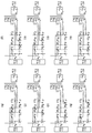
1 is a circuit diagram of a conventional dual-buck half-bridge converter. The dual-buck half-bridge converter comprises two switching elements S 1 and S 2 , diodes D 1 and D 2 , inductors L 1 and L 2 , capacitors C 1 and C 2 , 120). Power is transferred from AC voltage (V ac ) of AC part to DC part of load, and in the steady state, DC part voltage is larger than AC part peak value.
The dual-buck half-
The present embodiment has an object to provide an inductor with a dual-buck half-bridge circuit as a rectifier, thereby distributing the current capacity of the inductor to increase the efficiency and increase the capacity. Also, during the half period of the AC negative voltage, the first capacitor (C 1 ) And the second capacitor (C 2 ) voltage is always being discharged.
According to the example an aspect of this embodiment, for generating an alternating voltage (V ac) is applied is derived from the received primary winding, the primary winding first induced voltage (v ac1) and a second induced voltage (v ac2) for each two A transformer including a primary winding and a tertiary winding; An inductor group which receives a current from the secondary winding and the tertiary winding and generates a link voltage according to the current; A leg unit for receiving the link voltage and converting the link voltage into a DC voltage; A capacitor group which receives the DC voltage from the leg portion and performs charge / discharge; And a control unit for generating a control signal for controlling the switching of the leg unit for charging / discharging the capacitor group. The interleaved dual-buck converter of
According to another aspect of the present embodiment, is derived from a primary winding receiving applying an alternating voltage (V ac) in the transformer a first induced voltage (v ac1) and a second induced voltage (v ac2 to the third winding to the secondary winding Respectively; Receiving a current from the secondary winding and the tertiary winding in an inductor group and generating a link voltage according to the current; Receiving the link voltage from the leg portion and converting the link voltage into a DC voltage; Charging and discharging the DC voltage by receiving the DC voltage from the capacitor group; And controlling switching of the leg portion for charging / discharging the capacitor group. The method of controlling an interleaved dual-buck converter according to
As described above, the interleaved dual-buck converter according to the present embodiment includes PFC control, rectification and boosting operation, a first capacitor C 1 , And eliminating the voltage controllable section of the second capacitor (C 2 ) and distributing the inductor current. In addition, by distributing the dual-buck half-bridge circuit and applying the interleaved form, the current capacity of the inductor is divided, thereby improving efficiency and capacity of the entire bridge circuit.
1 is a circuit diagram of a conventional dual-buck half-bridge converter.
Figure 2 illustrates operational characteristics of a dual-buck half-bridge converter in accordance with an embodiment of the present invention.
3 is a block diagram of a controller of a dual-buck half-bridge converter in accordance with an embodiment of the present invention.
4 is a circuit diagram of an interleaved dual-buck converter in accordance with an embodiment of the present invention.
5 illustrates operational characteristics of an interleaved dual-buck converter in accordance with an embodiment of the present invention.
6 is a block diagram of a controller of an interleaved dual-buck converter in accordance with an embodiment of the present invention.
Figure 7 illustrates simulation parameters in accordance with an embodiment of the present invention.
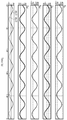
8 shows the current relationship between the AC negative voltage and current and L 1 and L 2 of a dual-buck half-bridge converter according to an embodiment of the present invention.
Figure 9 illustrates the AC negative and DC negative voltage relationships of a dual-buck half-bridge converter in accordance with an embodiment of the present invention.
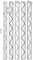
10 illustrates the current relationship between the AC negative voltage and current and L 1 and L 2 of an interleaved dual-buck converter according to an embodiment of the present invention.
11 shows the current relationship of the AC negative voltage, current, v ac2 voltage, current, L 3 and L 4 of the interleaved dual-buck converter according to an embodiment of the present invention.
12 illustrates the AC negative voltage and DC negative voltage relationships of an interleaved dual-buck converter according to an embodiment of the present invention.
Hereinafter, the present embodiment will be described in detail with reference to the accompanying drawings.
Figure 2 illustrates operational characteristics of a dual-buck half-bridge converter in accordance with an embodiment of the present invention. The
2 (a) shows a state in which the AC negative voltage is positive and S 1 is on. In this case, D 1 is turned off and i ac flows in a direction output from the AC negative voltage. On the other hand, C 1 And C 2 are both discharged. When D 1 is in an ON state, it can be expressed as shown in FIG. 2 (b). That is, S 1 is in the off state, and i ac decreases in the direction output from the AC negative voltage. On the other hand, C 1 is in a charged state and C 2 is in a discharged state. 2 (a) and 2 (b), when the AC negative voltage has a positive value, the current flows only to L 1 . C 1 is repeatedly charged and discharged by the switching operation, and C 2 is always discharged.
2 (c) shows a state in which the AC negative voltage is negative and S 2 is on. In this case, D2 is turned off and i ac flows in the direction of input to the AC negative voltage. C 1 and C 2 are all discharged. 2 (d) shows a state in which D 2 is on. At this time, S 2 is turned off, i ac flows decreases in the direction in which the input AC voltage part. C 2 changes to a charged state, and C 1 maintains a discharged state. As shown in (c) and (d) of FIG. 2, when the AC negative voltage has a negative value, the current flows only to L 2 . C 2 is repeatedly charged and discharged by the switching operation, and C 1 is always discharged.
As described above, the dual-buck half-
3 is a block diagram of a
The
The
The
The
The
A
The
The
When the AC negative voltage is a positive value, the
When the AC negative voltage is negative, the
The
4 is a circuit diagram of an interleaved dual-buck converter in accordance with an embodiment of the present invention. The interleaved dual-
The inductor groups L 1 , L 2 , L 3 , and
5 illustrates operational characteristics of an interleaved dual-buck converter in accordance with an embodiment of the present invention. The
(A) in FIG. 5 - (d) is AC portion (transformer primary side) is that the voltage is positive, v, and the value is a positive value of ac1 v from the value of the state of the value of the negative ac2, S 1, D 1 , S 4 , and D 4 , respectively. 5 (a) shows a state in which S 1 and S 4 are on and D 1 and D 4 are off. At this time, i ac1 increases in a direction output from the voltage v ac1 , and i ac2 decreases in a direction of input to the voltage v ac2 . On the other hand, both of C 1 and C 2 are in the discharge state. FIG. 5B shows a state in which D 1 and D 4 are on and S 1 and S 4 are off. At this time, i ac1 decreases in the direction output from the voltage v ac1 , and i ac2 decreases in the direction input to the voltage v ac2 . On the other hand, C 1 and C 2 are all in a charged state. FIG. 5C shows a state in which S 1 and D 4 are on and D 1 and S 4 are off. At this time, i ac1 increases in a direction output from the voltage v ac1 , and i ac2 decreases in a direction input to the voltage v ac2 . On the other hand, C 1 is in a discharged state and C 2 is in a charged state. 5D shows that D 1 and S 4 are on and S 1 and D 4 are off. At this time, i ac1 decreases in the direction output from the voltage v ac1 , and i ac2 increases in the direction input to the voltage v ac2 . At this time, i ac1 decreases in the direction output from the voltage v ac1 , and i ac2 increases in the direction input to the voltage v ac . On the other hand, C 1 becomes a charged state and C 2 becomes a discharged state.
When the AC negative voltage is a positive value, the operation of the interleaved dual-buck converter is summarized as follows: L 1 current flows in the direction always output from the voltage v ac1 and L 4 current flows in the direction always inputted from the voltage v ac2 Able to know. 5 (a) and 5 (c), when S 1 is in an on state, C 1 is in a discharge state. In (b) and (d) of FIG. 5, when S 1 is off, C 1 is in a charged state. From these results, it can be seen that when the AC negative voltage is a positive value, the voltage of C 1 can be controlled using S 1 , and the voltage of C 2 can be controlled using S 4 . Thus, unlike a dual-buck half-bridge converter, an interleaved dual-buck converter can control both C 1 and C 2 voltages during a positive half-cycle.
The following shows the operating characteristics according to the on / off states of S 2 , D 2 , S 3 , and D 3 with the AC negative voltage being a positive value. FIG. 5E shows a state in which S 2 and S 3 are on, and D 2 and D 3 are off. At this time, i ac1 increases in the direction of input to the voltage of v ac1 , and i ac2 increases in the direction of output from the voltage of v ac2 . On the other hand, both of C 1 and C 2 are in the discharge state. In FIG. 5 (g), S 2 and D 3 are on, and D 2 and S 3 are off. 5 (h) shows a state in which D 2 and S 3 are on and S 2 and D 3 are off. At this time, i ac1 decreases in the direction of input to the voltage v ac1 , and i ac2 increases in the direction output from the voltage v ac . On the other hand, C 1 is in a discharged state and C 2 is in a charged state.
When the AC negative voltage is negative, the operation of the interleaved dual-buck converter is summarized as follows. L 2 current flows in the direction of always entering the voltage of v ac1 , and L 3 current flows in the direction of always output from the voltage of v ac2 . 5 (e) and 5 (g), C 2 is in the discharge state when S 2 is on and C 1 is in the discharge state when S 2 is off in FIGS. 5 (f) do. Similarly, also in the 5 (e), when the S 3 from (h), and the condition C 1 is discharged, when the S 3 is turned off at (f), (g) of Figure 5 is C 1 The battery is in a charged state. From these results, it can be seen that the C 2 voltage can be controlled by S 2 when the AC negative voltage is negative, and the C 1 voltage can be controlled by S 3 . Thus, it is shown that both the C 1 and C 2 voltages can be controlled during the negative half period of the interleaved dual-
5, it can be seen that the interleaved dual-
6 is a block diagram of a controller of an interleaved dual-buck converter in accordance with an embodiment of the present invention. The
The
The
The
The
The
The
The
When V ac is positive, the
A
The first
The first
The second
When the AC negative voltage is a positive value, the positive terminal of the
When the AC negative voltage is negative, the positive terminal of the
When the AC negative voltage is a negative value, the positive terminal of the
When the AC negative voltage is a positive value, the positive terminal of the
Simulations were performed to analyze the operating characteristics of the circuits of FIGS. 1 and 4. A PSIM tool is used for the simulation, and the
Figure 7 illustrates simulation parameters in accordance with an embodiment of the present invention. The interleaved dual-
8 shows the current relationship between the AC negative voltage and current and L 1 and L 2 of a dual-buck half-bridge converter according to an embodiment of the present invention. Dual-buck half-bridge converter 100 v ac voltage is positive due to the S 1 ON / OFF operation flows, and the current is increased or decreased to L 1 when the value of a, v when the ac voltage is negative value of S 2 on / off Due to the operation, the current flows to L 2 with increasing or decreasing. At this time, i ac is the sum of one period of L 1 and L 2 currents, and the current peak value of L 1 and L 2 is equal to i ac .
Figure 9 illustrates the AC negative and DC negative voltage relationships of a dual-buck half-bridge converter in accordance with an embodiment of the present invention. The dual-buck half-
8 and 9, the dual-buck half-
10 illustrates the current relationship between the AC negative voltage and current and L 1 and L 2 of an interleaved dual-buck converter according to an embodiment of the present invention. When the v ac voltage is positive, the interleaved dual-
11 shows current relationships of AC negative voltage, current, v ac2 voltage, current, L 3 and L 4 of an interleaved dual-buck half-bridge converter according to an embodiment of the present invention. The interleaved dual-
12 illustrates the AC negative voltage and DC negative voltage relationships of an interleaved dual-buck half-bridge converter according to an embodiment of the present invention. The interleaved dual-
10, 11 and from the Figure 12, an interleaved dual according to the
The foregoing description is merely illustrative of the technical idea of the present embodiment, and various modifications and changes may be made to those skilled in the art without departing from the essential characteristics of the embodiments. Therefore, the present embodiments are to be construed as illustrative rather than restrictive, and the scope of the technical idea of the present embodiment is not limited by these embodiments. The scope of protection of the present embodiment should be construed according to the following claims, and all technical ideas within the scope of equivalents thereof should be construed as being included in the scope of the present invention.
120, 450:
310, 610: PLL 320:
330: Voltage controller 340: Multiplier
350: current controller 360: switch
370: inverter 380: comparator
420: transformer 422: primary winding
424: transformer core 426: secondary winding
428: Third winding
Claims (13)
An inductor group which receives a current from the secondary winding and the tertiary winding and generates a link voltage according to the current;
A leg unit for receiving the link voltage and converting the link voltage into a DC voltage;
A capacitor group which receives the DC voltage from the leg portion and performs charge / discharge; And
A control unit for generating a control signal for controlling switching of the leg unit for charging / discharging the capacitor group,
And an output terminal connected to the output terminal of the first transistor.
Wherein the AC voltage is applied to the primary winding and the first induced voltage having the same phase as the AC voltage is induced in the secondary winding and a phase opposite to the phase of the first induced voltage is induced in the tertiary winding And wherein the second inductive voltage having the second inductive voltage is induced.
Wherein the transformer is configured to generate a current of the same magnitude as the current flowing in the primary winding for one period of the AC voltage, to the secondary winding and the tertiary winding so that the primary winding, the secondary winding, And the winding ratio is 1: 1: 1. The interleaved dual-
A first inductor group including a first inductor L 1 and a second inductor L 2 , one end of which is connected in parallel, to one end of the secondary winding; And
And a third inductor L 3 including a third inductor L 3 and a fourth inductor L 4 , which are connected in parallel at one end,
And an output terminal coupled to the output terminal.
Wherein the secondary winding and the tertiary winding have a winding direction such that a phase of a current flowing to the first inductor group and a phase of a current flowing in the second inductor group are opposite to each other, And the other ends of the windings are connected to each other.
Wherein the capacitor group includes a first capacitor (C 1 ) and a second capacitor (C 2 ) connected in series between both terminals of the leg portion, wherein a connection end of the first capacitor and the second capacitor is connected to a terminal And the other end of the third winding is connected to the other end of the third winding.
A first converter receiving an output from the other end of the first inductor and generating a first converting voltage;
A second converter receiving an output from the other end of the second inductor to generate a second converting voltage;
A third converter receiving an output from the other end of the third inductor and generating a third converting voltage; And
A fourth converter for receiving an output from the other end of the fourth inductor and generating a fourth converting voltage,
And an output terminal connected to the output terminal of the first transistor.
The first converter includes:
A first diode (D 1) that one side is connected to the anode of the first inductor; And a first switch S 1 at one end to which the anode of the first diode is connected, the cathode of the first diode being connected to the positive terminal of the load and the other terminal of the first switch being connected to the negative terminal Lt; / RTI >
The second converter includes:
A second diode (D 2 ) having one side of the second inductor connected to the cathode; And once on and a second switch (S 2) that its cathode is connected to the second diode, the anode of the second diode is connected to the underlying negative terminal the other end of said second switch is a positive terminal of the load Lt; / RTI >
The third converter includes:
A third diode (D 3) is a side of the third inductor is connected to the anode; And one end to the anode of the third and the third and a third switch (S 3) which anode is connected to the diode, the diode is connected to the positive terminal of the load the other end of the third switch is in terms of the underlying negative terminal Lt; / RTI >
The fourth converter includes:
A fourth diode connected such that one end of the fourth inductor connected to the cathode (D 4); And one end and a fourth switch (S 4) such that its cathode is connected to the fourth diode to the anode of the fourth diode is connected to the underlying negative terminal the other end of the fourth switch is a positive terminal of the load To-analog converters.
When the first diode is turned on, the first switch is turned off. When the first diode is turned off, the first switch is turned on. When the second diode is turned on, the second switch is turned off , The second switch is turned on when the second diode is turned off, the third switch is turned off when the third diode is turned on, the third switch is turned on when the third diode is turned off, The fourth switch is turned off when the first diode is turned on, and the fourth switch is turned on when the fourth diode is turned off.
The first capacitor voltage is controlled using the first switch when the AC voltage is a positive value, the second capacitor voltage is controlled using the fourth switch, and when the AC voltage is a negative value, 2 switch to control the second capacitor voltage and to control the first capacitor voltage using the third switch to control the charge and discharge of the first capacitor and the second capacitor for one period, Interleaved dual-buck converter.
The current of the first inductor flows in a direction of outputting from the secondary winding and the current of the fourth inductor flows in a direction of input of the tertiary winding when the AC voltage is a positive value,
The second inductor current flows in a direction to be outputted from the secondary winding and the current of the third inductor flows in a direction to be input to the tertiary winding when the AC voltage is a negative value Interleaved dual-buck converter.
The first inductor Current of the second inductor The capacities of the first inductor and the fourth inductor are equal to each other so that a current of the first inductor, a current of the third inductor, and a current of the fourth inductor flows in half the current of the AC voltage.
Receiving a current from the secondary winding and the tertiary winding in an inductor group and generating a link voltage according to the current;
Receiving the link voltage from the leg portion and converting the link voltage into a DC voltage;
Charging and discharging the DC voltage by receiving the DC voltage from the capacitor group; And
A step of controlling switching of the leg portion for charging / discharging the capacitor group
And an output terminal connected to the output terminal of the inverter.
Priority Applications (1)
| Application Number | Priority Date | Filing Date | Title |
|---|---|---|---|
| KR1020150168956A KR101742231B1 (en) | 2015-11-30 | 2015-11-30 | High Power Factor And High Efficiency Interleaved Dual-Buck Converter And Method Therefor |
Applications Claiming Priority (1)
| Application Number | Priority Date | Filing Date | Title |
|---|---|---|---|
| KR1020150168956A KR101742231B1 (en) | 2015-11-30 | 2015-11-30 | High Power Factor And High Efficiency Interleaved Dual-Buck Converter And Method Therefor |
Publications (2)
| Publication Number | Publication Date |
|---|---|
| KR20170064100A true KR20170064100A (en) | 2017-06-09 |
| KR101742231B1 KR101742231B1 (en) | 2017-06-19 |
Family
ID=59219934
Family Applications (1)
| Application Number | Title | Priority Date | Filing Date |
|---|---|---|---|
| KR1020150168956A KR101742231B1 (en) | 2015-11-30 | 2015-11-30 | High Power Factor And High Efficiency Interleaved Dual-Buck Converter And Method Therefor |
Country Status (1)
| Country | Link |
|---|---|
| KR (1) | KR101742231B1 (en) |
Cited By (5)
| Publication number | Priority date | Publication date | Assignee | Title |
|---|---|---|---|---|
| CN107834882A (en) * | 2017-11-20 | 2018-03-23 | 西安许继电力电子技术有限公司 | A kind of double BUCK low-leakage currents single-phase inverters and its method of work |
| KR20200008439A (en) * | 2018-07-16 | 2020-01-28 | 현대자동차주식회사 | Electric vehicle and charging apparatus thereof |
| KR20210021586A (en) * | 2018-06-28 | 2021-02-26 | 비테스코 테크놀로지스 게엠베하 | Vehicle-side charging circuit |
| CN115483823A (en) * | 2022-09-21 | 2022-12-16 | 钰泰半导体股份有限公司 | Switching power factor corrector and AC/DC converter |
| KR102532877B1 (en) | 2021-11-16 | 2023-05-15 | 고려대학교 산학협력단 | A dual-phase dual-path buck-boost dc-dc converter with continuous input output currents and single-mode operation |
Family Cites Families (3)
| Publication number | Priority date | Publication date | Assignee | Title |
|---|---|---|---|---|
| TW200636420A (en) | 2004-12-14 | 2006-10-16 | Int Rectifier Corp | An EMI noise reduction circuit and method for bridgeless PFC circuit |
| JP5210331B2 (en) | 2010-01-06 | 2013-06-12 | 力銘科技股▲分▼有限公司 | Interleaved bridgeless power factor corrector and control method thereof |
| US9252656B2 (en) * | 2013-03-12 | 2016-02-02 | XP Power Limited | Bridgeless interleaved power factor correction circuit using a PFC inductor with quad-winding on a single core |
-
2015
- 2015-11-30 KR KR1020150168956A patent/KR101742231B1/en active IP Right Grant
Cited By (6)
| Publication number | Priority date | Publication date | Assignee | Title |
|---|---|---|---|---|
| CN107834882A (en) * | 2017-11-20 | 2018-03-23 | 西安许继电力电子技术有限公司 | A kind of double BUCK low-leakage currents single-phase inverters and its method of work |
| KR20210021586A (en) * | 2018-06-28 | 2021-02-26 | 비테스코 테크놀로지스 게엠베하 | Vehicle-side charging circuit |
| KR20200008439A (en) * | 2018-07-16 | 2020-01-28 | 현대자동차주식회사 | Electric vehicle and charging apparatus thereof |
| KR102532877B1 (en) | 2021-11-16 | 2023-05-15 | 고려대학교 산학협력단 | A dual-phase dual-path buck-boost dc-dc converter with continuous input output currents and single-mode operation |
| CN115483823A (en) * | 2022-09-21 | 2022-12-16 | 钰泰半导体股份有限公司 | Switching power factor corrector and AC/DC converter |
| CN115483823B (en) * | 2022-09-21 | 2024-01-19 | 钰泰半导体股份有限公司 | Switching power factor corrector and AC/DC converter |
Also Published As
| Publication number | Publication date |
|---|---|
| KR101742231B1 (en) | 2017-06-19 |
Similar Documents
| Publication | Publication Date | Title |
|---|---|---|
| JP6569839B1 (en) | Power converter | |
| US10044278B2 (en) | Power conversion device | |
| KR101742231B1 (en) | High Power Factor And High Efficiency Interleaved Dual-Buck Converter And Method Therefor | |
| US11056979B2 (en) | Power conversion apparatus | |
| US8441237B2 (en) | Power factor correction (PFC) circuit and method therefor | |
| JP2013504295A (en) | Electrical energy conversion circuit device | |
| JP2010519890A (en) | Three-phase, high power uninterruptible power supply | |
| WO2019216180A1 (en) | Dc power transformation system | |
| EP2975753B1 (en) | A three-level converter | |
| WO2013136378A1 (en) | Power conversion apparatus | |
| KR20190115364A (en) | Single and three phase combined charger | |
| Li et al. | Optimal synergetic control of a three-phase two-stage ultra-wide output voltage range EV battery charger employing a novel hybrid quantum series resonant DC/DC converter | |
| US20230074022A1 (en) | Power converter topologies with power factor correction circuits controlled using adjustable deadtime | |
| Sayed et al. | New PWM technique for grid-tie isolated bidirectional DC-AC inverter based high frequency transformer | |
| TWI551024B (en) | Ac-dc power conversion device and control method thereof | |
| Sayed et al. | Modeling and control of bidirectional isolated battery charging and discharging converter based high-frequency link transformer | |
| KR20150101913A (en) | Method for battery charging control and apparatus therefor | |
| EP4113813A1 (en) | Power electronic apparatus for converting input ac into dc | |
| US20230071003A1 (en) | Power factor correction circuits controlled using adjustable deadtime | |
| Takahashi et al. | Power decoupling method for isolated DC to single-phase AC converter using matrix converter | |
| US20230076369A1 (en) | Unidirectional power converters with power factor correction circuits controlled using adjustable deadtime | |
| US20230322105A1 (en) | Charging device and method for operating the charging device | |
| KR20180091543A (en) | Power factor correction converter | |
| JP5748804B2 (en) | Power converter | |
| Askarian et al. | A new control method for a novel isolated, bridgeless single-stage AC/DC converter used in industrial battery chargers |
Legal Events
| Date | Code | Title | Description |
|---|---|---|---|
| A201 | Request for examination | ||
| E902 | Notification of reason for refusal | ||
| AMND | Amendment | ||
| E601 | Decision to refuse application | ||
| AMND | Amendment | ||
| E90F | Notification of reason for final refusal | ||
| AMND | Amendment | ||
| X701 | Decision to grant (after re-examination) | ||
| GRNT | Written decision to grant |