KR20110005834A - Blade architecture array converter - Google Patents
Blade architecture array converter Download PDFInfo
- Publication number
- KR20110005834A KR20110005834A KR1020107024596A KR20107024596A KR20110005834A KR 20110005834 A KR20110005834 A KR 20110005834A KR 1020107024596 A KR1020107024596 A KR 1020107024596A KR 20107024596 A KR20107024596 A KR 20107024596A KR 20110005834 A KR20110005834 A KR 20110005834A
- Authority
- KR
- South Korea
- Prior art keywords
- current
- signal
- converter
- direct current
- converters
- Prior art date
Links
Images


Classifications
-
- H—ELECTRICITY
- H02—GENERATION; CONVERSION OR DISTRIBUTION OF ELECTRIC POWER
- H02M—APPARATUS FOR CONVERSION BETWEEN AC AND AC, BETWEEN AC AND DC, OR BETWEEN DC AND DC, AND FOR USE WITH MAINS OR SIMILAR POWER SUPPLY SYSTEMS; CONVERSION OF DC OR AC INPUT POWER INTO SURGE OUTPUT POWER; CONTROL OR REGULATION THEREOF
- H02M7/00—Conversion of ac power input into dc power output; Conversion of dc power input into ac power output
- H02M7/42—Conversion of dc power input into ac power output without possibility of reversal
- H02M7/44—Conversion of dc power input into ac power output without possibility of reversal by static converters
- H02M7/48—Conversion of dc power input into ac power output without possibility of reversal by static converters using discharge tubes with control electrode or semiconductor devices with control electrode
- H02M7/493—Conversion of dc power input into ac power output without possibility of reversal by static converters using discharge tubes with control electrode or semiconductor devices with control electrode the static converters being arranged for operation in parallel
-
- H—ELECTRICITY
- H02—GENERATION; CONVERSION OR DISTRIBUTION OF ELECTRIC POWER
- H02J—CIRCUIT ARRANGEMENTS OR SYSTEMS FOR SUPPLYING OR DISTRIBUTING ELECTRIC POWER; SYSTEMS FOR STORING ELECTRIC ENERGY
- H02J3/00—Circuit arrangements for ac mains or ac distribution networks
- H02J3/38—Arrangements for parallely feeding a single network by two or more generators, converters or transformers
- H02J3/381—Dispersed generators
-
- H—ELECTRICITY
- H02—GENERATION; CONVERSION OR DISTRIBUTION OF ELECTRIC POWER
- H02J—CIRCUIT ARRANGEMENTS OR SYSTEMS FOR SUPPLYING OR DISTRIBUTING ELECTRIC POWER; SYSTEMS FOR STORING ELECTRIC ENERGY
- H02J3/00—Circuit arrangements for ac mains or ac distribution networks
- H02J3/38—Arrangements for parallely feeding a single network by two or more generators, converters or transformers
- H02J3/40—Synchronising a generator for connection to a network or to another generator
- H02J3/44—Synchronising a generator for connection to a network or to another generator with means for ensuring correct phase sequence
-
- H—ELECTRICITY
- H02—GENERATION; CONVERSION OR DISTRIBUTION OF ELECTRIC POWER
- H02J—CIRCUIT ARRANGEMENTS OR SYSTEMS FOR SUPPLYING OR DISTRIBUTING ELECTRIC POWER; SYSTEMS FOR STORING ELECTRIC ENERGY
- H02J3/00—Circuit arrangements for ac mains or ac distribution networks
- H02J3/38—Arrangements for parallely feeding a single network by two or more generators, converters or transformers
- H02J3/46—Controlling of the sharing of output between the generators, converters, or transformers
-
- H—ELECTRICITY
- H02—GENERATION; CONVERSION OR DISTRIBUTION OF ELECTRIC POWER
- H02J—CIRCUIT ARRANGEMENTS OR SYSTEMS FOR SUPPLYING OR DISTRIBUTING ELECTRIC POWER; SYSTEMS FOR STORING ELECTRIC ENERGY
- H02J2300/00—Systems for supplying or distributing electric power characterised by decentralized, dispersed, or local generation
- H02J2300/20—The dispersed energy generation being of renewable origin
- H02J2300/22—The renewable source being solar energy
- H02J2300/24—The renewable source being solar energy of photovoltaic origin
-
- H—ELECTRICITY
- H02—GENERATION; CONVERSION OR DISTRIBUTION OF ELECTRIC POWER
- H02J—CIRCUIT ARRANGEMENTS OR SYSTEMS FOR SUPPLYING OR DISTRIBUTING ELECTRIC POWER; SYSTEMS FOR STORING ELECTRIC ENERGY
- H02J2300/00—Systems for supplying or distributing electric power characterised by decentralized, dispersed, or local generation
- H02J2300/20—The dispersed energy generation being of renewable origin
- H02J2300/28—The renewable source being wind energy
-
- H—ELECTRICITY
- H02—GENERATION; CONVERSION OR DISTRIBUTION OF ELECTRIC POWER
- H02M—APPARATUS FOR CONVERSION BETWEEN AC AND AC, BETWEEN AC AND DC, OR BETWEEN DC AND DC, AND FOR USE WITH MAINS OR SIMILAR POWER SUPPLY SYSTEMS; CONVERSION OF DC OR AC INPUT POWER INTO SURGE OUTPUT POWER; CONTROL OR REGULATION THEREOF
- H02M1/00—Details of apparatus for conversion
- H02M1/0064—Magnetic structures combining different functions, e.g. storage, filtering or transformation
-
- H—ELECTRICITY
- H02—GENERATION; CONVERSION OR DISTRIBUTION OF ELECTRIC POWER
- H02M—APPARATUS FOR CONVERSION BETWEEN AC AND AC, BETWEEN AC AND DC, OR BETWEEN DC AND DC, AND FOR USE WITH MAINS OR SIMILAR POWER SUPPLY SYSTEMS; CONVERSION OF DC OR AC INPUT POWER INTO SURGE OUTPUT POWER; CONTROL OR REGULATION THEREOF
- H02M3/00—Conversion of dc power input into dc power output
- H02M3/02—Conversion of dc power input into dc power output without intermediate conversion into ac
- H02M3/04—Conversion of dc power input into dc power output without intermediate conversion into ac by static converters
- H02M3/10—Conversion of dc power input into dc power output without intermediate conversion into ac by static converters using discharge tubes with control electrode or semiconductor devices with control electrode
- H02M3/145—Conversion of dc power input into dc power output without intermediate conversion into ac by static converters using discharge tubes with control electrode or semiconductor devices with control electrode using devices of a triode or transistor type requiring continuous application of a control signal
- H02M3/155—Conversion of dc power input into dc power output without intermediate conversion into ac by static converters using discharge tubes with control electrode or semiconductor devices with control electrode using devices of a triode or transistor type requiring continuous application of a control signal using semiconductor devices only
- H02M3/156—Conversion of dc power input into dc power output without intermediate conversion into ac by static converters using discharge tubes with control electrode or semiconductor devices with control electrode using devices of a triode or transistor type requiring continuous application of a control signal using semiconductor devices only with automatic control of output voltage or current, e.g. switching regulators
- H02M3/158—Conversion of dc power input into dc power output without intermediate conversion into ac by static converters using discharge tubes with control electrode or semiconductor devices with control electrode using devices of a triode or transistor type requiring continuous application of a control signal using semiconductor devices only with automatic control of output voltage or current, e.g. switching regulators including plural semiconductor devices as final control devices for a single load
- H02M3/1584—Conversion of dc power input into dc power output without intermediate conversion into ac by static converters using discharge tubes with control electrode or semiconductor devices with control electrode using devices of a triode or transistor type requiring continuous application of a control signal using semiconductor devices only with automatic control of output voltage or current, e.g. switching regulators including plural semiconductor devices as final control devices for a single load with a plurality of power processing stages connected in parallel
- H02M3/1586—Conversion of dc power input into dc power output without intermediate conversion into ac by static converters using discharge tubes with control electrode or semiconductor devices with control electrode using devices of a triode or transistor type requiring continuous application of a control signal using semiconductor devices only with automatic control of output voltage or current, e.g. switching regulators including plural semiconductor devices as final control devices for a single load with a plurality of power processing stages connected in parallel switched with a phase shift, i.e. interleaved
-
- Y—GENERAL TAGGING OF NEW TECHNOLOGICAL DEVELOPMENTS; GENERAL TAGGING OF CROSS-SECTIONAL TECHNOLOGIES SPANNING OVER SEVERAL SECTIONS OF THE IPC; TECHNICAL SUBJECTS COVERED BY FORMER USPC CROSS-REFERENCE ART COLLECTIONS [XRACs] AND DIGESTS
- Y02—TECHNOLOGIES OR APPLICATIONS FOR MITIGATION OR ADAPTATION AGAINST CLIMATE CHANGE
- Y02E—REDUCTION OF GREENHOUSE GAS [GHG] EMISSIONS, RELATED TO ENERGY GENERATION, TRANSMISSION OR DISTRIBUTION
- Y02E10/00—Energy generation through renewable energy sources
- Y02E10/50—Photovoltaic [PV] energy
- Y02E10/56—Power conversion systems, e.g. maximum power point trackers
-
- Y—GENERAL TAGGING OF NEW TECHNOLOGICAL DEVELOPMENTS; GENERAL TAGGING OF CROSS-SECTIONAL TECHNOLOGIES SPANNING OVER SEVERAL SECTIONS OF THE IPC; TECHNICAL SUBJECTS COVERED BY FORMER USPC CROSS-REFERENCE ART COLLECTIONS [XRACs] AND DIGESTS
- Y02—TECHNOLOGIES OR APPLICATIONS FOR MITIGATION OR ADAPTATION AGAINST CLIMATE CHANGE
- Y02E—REDUCTION OF GREENHOUSE GAS [GHG] EMISSIONS, RELATED TO ENERGY GENERATION, TRANSMISSION OR DISTRIBUTION
- Y02E10/00—Energy generation through renewable energy sources
- Y02E10/70—Wind energy
- Y02E10/76—Power conversion electric or electronic aspects
Abstract
직류 전류를 펄스 진폭 변조된(pulse amplitude modulated, "PAM") 전류로 변환하는 컨버터, 즉 "PAMCC(pulse amplitude modulated current converter)"가 개개의 직류 전류원에 연결된다. 일부 실시예는 어레이, 예컨대 다수의 태양발전 패널들 내 각각의 직류 전류원에 대해 PAMCC를 제공한다. PAMCC는 직류 전류를 받고 그 출력단에서 PAM 전류를 제공한다. 펄스는 펄스의 시퀀스에 변조된 신호에 대하여 고주파수로 생성된다. 펄스의 시퀀스에 변조된신호는 낮은 주파수의 사인파 또는 DC를 포함한 다른 낮은 주파수의 파형의 일부를 대표할 수 있다. PAMCC의 출력이 유사한 PAMCC의 출력과 병렬로 연결되는 경우, PAMCC의 어레이가 형성되며, PAMCC의 출력 펄스는 서로에 대하여 이위상된다. 본 발명에 따라 구성된 PAMCC의 어레이는, 결합된 출력이 각각의 PAMCC에 의해 변조된 전류 펄스 진폭의 복조된 합과 같은 분산된 다상 인버터를 형성한다. A converter that converts direct current into pulse amplitude modulated ("PAM") currents, or "pulse amplitude modulated current converter" (PAMCC), is connected to an individual direct current source. Some embodiments provide a PAMCC for each direct current source in an array, such as multiple solar panels. The PAMCC receives a direct current and provides a PAM current at its output. Pulses are generated at high frequencies for signals modulated to a sequence of pulses. The signal modulated to a sequence of pulses may represent a portion of a low frequency sine wave or other low frequency waveform, including DC. When the outputs of the PAMCCs are connected in parallel with the outputs of similar PAMCCs, an array of PAMCCs is formed and the output pulses of the PAMCCs are out of phase with respect to each other. An array of PAMCCs constructed in accordance with the present invention form a distributed polyphase inverter such that the combined output is a demodulated sum of the current pulse amplitude modulated by each PAMCC.

Description
본원은 Kernahan 등에 의해 2008년 4월 2일에 출원된 미국 정규출원번호 12/061,025, 발명의 명칭 "DISTRIBUTED MULTIPHASE CONVERTERS"의 CIP(Continuation-in-Part) 출원이며, 그 내용 전체가 본 명세서에 도입되며, 해당 출원을 기초로 우선권을 주장한다. This application is a CIP (Continuation-in-Part) application of US Patent Application No. 12 / 061,025, entitled "DISTRIBUTED MULTIPHASE CONVERTERS", filed April 2, 2008, issued by Kernahan et al., The entire contents of which are incorporated herein by reference. And claim priority on the basis of the application.
인류의 활동에 의해 야기된 온난화에 대한 우려, 비용 증가 및 사용가능한 석유 및 천연가스의 잠재적인 부족, 수력 발전을 위한 물의 부족과 같은 많은 이유로 인해, 에너지를 제공하기 위한 비용-효율적인 방법 및 물질에 관심이 매우 크다. 재생 가능한 에너지원에 대해 관심이 집중되고 있으며, 특히 태양광발전 패널에 대해 관심이 집중되고 있다. 현재, 태양발전 장비로부터 얻은 전기 용량이 광범위한 사용 및 설치가 많은 요인에 의해 방해받고 있다. 이러한 해결책은 낮은 효율, 짧은 제품 수명, 열악한 비지니스 모델, 소비자가 자본비용을 회수하기에 충분히 오랫동안 태양발전 장비가 구비된 시설에서 거주하지 않는 경우 회수될 수 없을 수 있는 상당한 선불 비용에 대한 소비자의 반감과 같은 문제점이 존재한다. For many reasons, such as concerns about warming caused by human activities, increased costs and potential shortages of available oil and natural gas, and lack of water for hydropower, Interest is very big. There is a growing interest in renewable energy sources, particularly in photovoltaic panels. At present, the electrical capacity obtained from solar power equipment is hampered by many factors due to its widespread use and installation. This solution is a low half-life for consumers, with low efficiency, short product life, poor business models, and significant upfront costs that may not be recoverable if they do not live in a facility equipped with solar power equipment long enough to recover capital costs. The same problem exists.
이러한 문제점 중 효율 또는 낮은 효율이 가장 주된 문제점이다. 예를 들어, 도 1을 참조하면, 종래기술은 직렬로 연결된 다수의 태양광 패널을 제공하며, 그리고 나서 패널로부터 획득된 전력은 직류 전류에서 교류 전류로 변환된다. 그러나, 패널 스트링의 효율은 직렬 연결된 패널들 중 어느 하나에 의한 감소된 출력으로 인해 극도로 감소된다. 감소된 출력의 원인은 새가 떨어지는 것으로부터 일련의 패널들 중 일부가 돌출된 나무에 의해 그늘지거나 부분적으로 그늘지는 것이 있다. Among these problems, efficiency or low efficiency is the main problem. For example, referring to FIG. 1, the prior art provides a number of solar panels connected in series, and then the power obtained from the panels is converted from direct current to alternating current. However, the efficiency of the panel string is extremely reduced due to the reduced output by either of the series connected panels. The cause of the reduced output is that some of the panels in the series are shaded or partially shaded by protruding trees from falling birds.
도 2는 계통연계형(grid-connected) 태양광발전 시스템의 일 예이며, 태양발전 시스템에 의해 제공된 전력은 공익 사업의 그리드 시스템으로 구동된다. 종래기술에 따른 시스템의 대표적인 구성(202)은 패널에 의해 제공된 직류 전류를 교류 전류의 전력으로 으로 변환하는 단일의 인버터를 구비한 복수의 패널들을 도시한다. 본 발명의 예시적인 실시예의 대표가 시스템(204)으로 도시된다. (204)의 각각의 패널이 컨버터를 포함한다. 2 is an example of a grid-connected photovoltaic system, wherein the power provided by the solar system is driven by a grid system of utility.
부분적으로 패널의 중량 및 부수적인 구조적 요구조건으로 인해 설치 비용이 높다. 추가적으로, 각각의 패널이 직렬로 연결됨에 따라 형성된 고전압 DC 회로가 패널에 조명이 비춰지는 때면 항상 전력을 공급하므로, 패널의 설치는 위험할 수 있다. 중량 및 안전성에 대한 요인은, 설치를 위해 적어도 두 명의 인원을 포함한 작업자를 요구한다. Installation costs are high, in part due to the weight of the panels and the accompanying structural requirements. In addition, the installation of the panel can be dangerous because the high voltage DC circuit formed as each panel is connected in series always supplies power when the panel is illuminated. Factors for weight and safety require an operator with at least two people for installation.
현재, 중앙집중형 인버터의 사용은 태양광 패널과 인버터 간의 분리를 요구한다. 대부분의 경우, 이러한 분리는 상당히 이격되어 구성되며; 수 피트만큼 이격된다. 전도체 상에서 DC 전력을 전달할 때 전력 손실이 일어나는 주된 원인이 전류의 제곱에 컨덕터의 저항을 곱한만큼에 해당되고 낮은 저항의 전도체가는 고비용이고 작업이 어렵기 때문에, 중앙집중화된 인버터를 사용할 경우 높은 DC 전압이 선호된다. 높은 DC 전압을 달성하는 한 방법은 태양광 패널을 직렬로 배열하는 것이다. 이는, 스트링 중 높은 전압단에서 태양광 패널은 높은 전압, 일반적으로 수백 볼트 그리고 일부의 경우 거의 천 볼트에 가까운 전압으로 그 내부 회로 전부를 구비함을 의미한다. 사망, 부상, 아킹(arcing) 및 화재를 방지하기 위해, 이러한 패널의 내부 회로는 절연성이 우수해야 한다. 바람직한 절연성 재질은 유리이며, 이는 태양광 패널에 상당한 비용 및 중량을 유발할 수 있다. 본 발명은 그와 관련된 태양광 패널의 내부적인 태양광발전을 거의 중성점에 가까이 유지한다. 많은 실시예에서, 태양광발전 다이오드의 내부 세트 중 어떠한 부분도 중성점으로부터 수십 볼트 이상 떨어져 있지 않으며, 이는 접지와 매우 가깝다. 어레이 컨버터의 고전압부는 물리적으로 매우 작으며, 이는 수 제곱인치의 크기를 가지며, 일반적으로 태양광 패널 어셈블리의 뒷부분에 물리적으로 배치된다. 이러한 배치는, 수백 볼트의 전압을 견디도록 어셈블리의 전방에서 수 제곱피트를 절연시켜야 하는 종래의 모듈과 비교하여 절연이 간단하고 가벼운 중량을 가진다. Currently, the use of a centralized inverter requires separation between the solar panel and the inverter. In most cases, this separation consists of quite spaces; Spaced several feet apart. High DC voltage when using a centralized inverter is the main cause of power loss when delivering DC power on a conductor, as the square of the current multiplied by the conductor's resistance and the low resistance conductor is expensive and difficult to work with. This is preferred. One way to achieve a high DC voltage is to arrange the solar panels in series. This means that at high voltage stages of the string, the solar panel has all of its internal circuits at a high voltage, typically hundreds of volts and in some cases almost a thousand volts. To prevent death, injury, arcing, and fire, the internal circuits of these panels must have good insulation. Preferred insulating materials are glass, which can result in significant cost and weight for solar panels. The present invention keeps the internal photovoltaic power generation of the solar panels associated therewith close to neutral. In many embodiments, no portion of the internal set of photovoltaic diodes is more than a few tens of volts from the neutral, which is very close to ground. The high voltage portion of the array converter is physically very small, which is several square inches in size, and is typically physically located at the rear of the solar panel assembly. This arrangement is simpler to insulate and has a lighter weight than conventional modules that must insulate several square feet in front of the assembly to withstand voltages of hundreds of volts.
태양광 패널의 제조사는 태양광 패널이 적어도 25년은 견딜 것으로 예상한다. 그러나, 오늘날 설비에 사용되는 인버터는 매우 크고 높은 커패시턴스의 전해 커패시터를 필요로 한다. 이러한 커패시터는 온도의 영향을 받으며, 특히 천장에서의 고온에 의해 그 수명이 단축된다. 결과적으로, 이러한 커패시터 내의 액체는 캐니스터로부터 누수될 것이며, 경험상 적어도 5년마다 교체되어야 한다. 이는 소유자가 부담하는 총 비용을 증가시킨다. 전해 커패시터(302)를 포함하는 예시적인 회로가 도 3에 도시된다. Solar panel manufacturers expect solar panels to last at least 25 years. However, inverters used in today's installations require very large and high capacitance electrolytic capacitors. Such capacitors are affected by temperature, and their life is shortened, especially by high temperatures in the ceiling. As a result, the liquid in these capacitors will leak from the canister and must be replaced at least every five years in experience. This increases the total cost to the owner. An example circuit including an
설치 후에도, 안전성이 우려된다. 태양광 패널은, 이들이 위험해질 수 있는 화재, 태풍 또는 다른 재난 발생 시 사용불능으로 만들기 위한 어떠한 수단도 구비하지 않는다. 예를 들어, 소방관은 주로 화재에 대한 최선의 접근책으로 지붕을 통하여 진입하므로, 지붕에 구멍을 뚫는다. 소방관이 소방용 도끼로 태양광 패널 또는 그와 연결된 와이어에 구멍을 뚫어야만 하는 경우, 특히 소방관 또는 그의 도끼가 접지 전위와 접촉하는 경우, 그 결과는 치명적일 수 있다. Even after installation, safety is a concern. Solar panels do not have any means to render them unusable in the event of a fire, typhoon or other disaster that can be dangerous. Firefighters, for example, often go through the roof as the best approach to the fire, so they drill holes in the roof. The result can be fatal if the firefighter must drill a hole in the solar panel or the wire connected to it with the fire axe, especially if the fireman or his ax contacts ground potential.
따라서, 효율을 개선하고, 시스템의 전체 수명을 연장시키고, 소비자가 얻기 위한 비용을 낮추는 비지니스 모델을 조장하고, 설치 도중 및 설치 후에도 안전하게 조작될 수 있는 시스템의 컴포넌트를 제공하는 수단이 요구된다. Accordingly, what is needed is a means to improve the efficiency, to extend the overall life of the system, to promote a business model that lowers the cost for the consumer, and to provide components of the system that can be safely operated during and after installation.
본 발명은 펄스 진폭 변조된 전류 컨버터를 제공하는 것을 목적으로 한다. It is an object of the present invention to provide a pulse amplitude modulated current converter.
많은 종래기술의 시스템에서, "마이크로 인버터"로 불리는 소형 인버터가 태양광 패널에 연결되어, 완전한 DC/AC 모듈을 형성한다. 모듈은, 예를 들어 부하로 220 볼트 60 Hz의 교류 전력을 제공한다. 이러한 복수의 모듈들은 (위상 동기 요구조건을 수반하여) 병렬로 연결되어 추가적인 전력 용량을 제공한다. 반면, 본 발명의 일 실시예에서, 태양광 패널은 DC 전류를 펄스 진폭 전류 컨버터로 제공하여 DC에서 펄스 진폭 전류로 변환하는 컨버터 모듈, 즉 "PAMCC"를 형성한다. 단일 PAMCC의 출력은 설계된 전력을 제공하지 않지만, 복수의 PAMCC들의 출력이 이위상되고(out of phase) 합하여, 그에 의해, 부하로 전력을 공급하는 분산된 다상 컨버터 시스템을 형성한다. In many prior art systems, small inverters called "micro inverters" are connected to the solar panel to form a complete DC / AC module. The module provides, for example, 220 volts 60 Hz alternating current power to the load. These multiple modules are connected in parallel (with phase synchronization requirements) to provide additional power capacity. On the other hand, in one embodiment of the present invention, the solar panel forms a converter module, or "PAMCC," which provides DC current to the pulse amplitude current converter to convert from DC to pulse amplitude current. The output of a single PAMCC does not provide the designed power, but the outputs of the plurality of PAMCCs are out of phase and thereby form a distributed polyphase converter system that powers the load.
종래기술에서, 큰 전해 커패시터는 직류 전기전류를 교류 전류로 변환하기 위해 시스템의 일부로 구성된다. 종래기술의 해결책은 불연속적인 입력 전류를 가지며, 광자를 전기 전류로 변환하는 태양광발전 셀을 통해 이러한 불연속적인 흐름을 연속적인 전류 흐름으로 변환하도록 컨 커패시터를 필요로 한다. 본 발명에서, 전류 모드의 입력 및 출력은 커패시터의 사이즈를 전해 기술(또는 다른 휘발성 액체를 기반으로 한 기술)에서 요구하는 조건 미만으로 줄일 수 있다. 사인파 재구성을 위한 에너지 저장은 태양광발전 다이오드로부터의 연속 모드 전류 입력을 사용하여 유도성으로 수행된다. 이는 펄스 성형에 대한 커패시터의 역할을 줄인다. 설계의 신뢰성은 반도체 마지닝(margining), 인덕터 절연과 코어 물질 마진, 및 열적 사이클 중심의 기계적 응력에 의해 지배된다. 전해 커패시터가 제거되는 기술적 제한으로, 25년을 초과하는 수명이 가능해진다. In the prior art, large electrolytic capacitors are constructed as part of a system to convert direct current electrical current into alternating current. Prior art solutions have a discontinuous input current and require a condenser to convert this discontinuous flow into a continuous current flow through a photovoltaic cell that converts photons into electrical current. In the present invention, the input and output of the current mode can reduce the size of the capacitor below the conditions required by electrolytic techniques (or other volatile liquid based techniques). Energy storage for sine wave reconstruction is performed inductively using continuous mode current input from the photovoltaic diode. This reduces the role of the capacitor on pulse shaping. Design reliability is governed by semiconductor margining, inductor insulation and core material margin, and thermal cycle-oriented mechanical stress. Due to the technical limitation that electrolytic capacitors are removed, a lifespan of more than 25 years is possible.
모듈-그리드 인터페이스에서의 높은 전압은 인터페이스에서의 일반적인 전류를 약 7 배만큼 감소시키며, 저항에 대해 견디는 기능을 약 50 배만큼 개선시킨다. 커넥터 시스템을 수십 mΩ에서 수 Ω으로 이동시키는 것은 접촉면 및 물질의 요구조건을 감소시키는 동시에, 산화 및 오염에 대한 내성을 증가시킨다. 예를 들어: 200 W, 200 V의 두 개의 위상 어레이 컨버터는 910 mA를 요구하며, 1 퍼센트의 전력 손실에 대해 약 2.4 Ω의 상호연결 저항까지 견딜 수 있다. 반대로, 직렬로 연결된 스트링으로 집적된 30 V의 DC 전압, 200 W의 종래의 태양광 패널은 약 6.6 amp를 요구할 것이며, 동일한 1 퍼센트의 전력 손실에 대해 0.045 Ω의 상호연결 저항까지만 견딜 수 있다. The high voltage at the module-grid interface reduces the typical current at the interface by about seven times and improves the resistance to resistance by about 50 times. Moving the connector system from tens of mΩ to several ohms reduces contact surface and material requirements while increasing resistance to oxidation and contamination. For example: Two phase array converters, 200 W and 200 V, require 910 mA and can withstand up to approximately 2.4 Ω interconnect resistance for 1 percent power loss. Conversely, a 30 V DC voltage, 200 W conventional solar panel integrated into a string connected in series would require about 6.6 amps and could only withstand an interconnect resistance of 0.045 Ω for the same 1 percent power loss.
어레이 컨버터 구조에서, 두 위상 모두에 대한 전류 경로는 양방향으로 동일한 코일을 지나간다. 이는 두 위상 모두에서 동일한 전류의 흐름을 유발한다. In an array converter structure, the current paths for both phases pass through the same coil in both directions. This causes the same current flow in both phases.
검출된 그리드 이상, 예컨대 한도를 벗어난 전압 또는 국부적이거나 원격적으로 발생된 셧 다운 명령의 경우, 본 발명의 패널은 안전 상태로 셧 다운된다. 이러한 상태에서, 내부의 PV 어레이는 개방 회로가 되며, 내부의 인덕터는 방전되며, 내부의 전력 반도체는 개방 회로가 된다. 이러한 상태에서, 소방관의 도끼는 내부의 PV 어레이의 개방 회로 전압, 일반적으로 40 V만을 경험할 것이다. 내부의 PV 어레이의 안전 상태가 개방된 상태이므로, 도끼가 전류 또는 전압을 경험하기 위해서는 두 개의 단락 회로(하나는 접지됨)가 형성되어야 할 것이다. In the case of a detected grid abnormality, such as an out of limit voltage or a locally or remotely issued shutdown command, the panel of the present invention is shut down to a safe state. In this state, the internal PV array is an open circuit, the internal inductor is discharged, and the internal power semiconductor is an open circuit. In this condition, the firefighter's ax will only experience the open circuit voltage of the internal PV array, typically 40 V. Since the safety state of the internal PV array is open, two short circuits (one grounded) would have to be formed in order for the ax to experience current or voltage.
밸런스가 유지된 어레이 컨버터의 토폴로지로 인해, 음극이 중립점 아래에 위치하는 동일한 전압만큼 다이오드 어레이로의 양극이 중립점 위에 위치하는 경향을 가질 것이다. 이는 DC 아크 전압이 최소 스트라이크 전위보다 매우 낮은 값을 가지도록 한다. PV 다이오드 어레이 내에 AC 컴포넌트를 거의 대부분 제거하면서(연속 도전 모드의 입력 전류에 의함) 이러한 방식으로 내부 어레이 전압을 제한하는 것은, 고 전압 DC 스트링 적용분야에서 발견되는 접지 명세사항에 대한 엄밀한 누설 경로를 필요로 하지 않게 한다. 이는 PV 다이오드 어레이의 가장자리와 모듈의 프레임, 및 내부 어레이의 뒷부분과 모듈의 뒷부분 사이의 모듈 구조를 단순화시킨다. 예를 들어: 접지된 프레임과 내부 PV 다이오드 어레이 사이의 최대 450 V 직렬 연결된 스트링 패널의 누설에 대한 요구조건이 2 μA인 경우, 절연에 대한 요구조건은 225 MΩ이다. PV 다이오드 어레이와 중립점 간의 최대 30 V의 어레이 컨버터에서, 동일한 누설은 오직 15 MΩ의 절연만을 요구할 수 있다. 접지에 대한 PV 다이오드 어레이의 얼마 안되는 낮은 동작 전압은 또한 낮은 전압 스파크 간격과 MOV 컴포넌트를 사용할 수 있게 하여, 벼락 및 코로나 방전(안테나)과 다른 고 전압 현상에 대한 접지 경로를 개선시킨다. Due to the balanced topology of the array converter, the anode to the diode array will tend to be above the neutral point by the same voltage where the cathode is below the neutral point. This allows the DC arc voltage to have a value that is much lower than the minimum strike potential. Limiting the internal array voltage in this way, while eliminating almost all of the AC components in the PV diode array (by input current in continuous conduction mode), provides a tight leakage path for grounding specifications found in high voltage DC string applications. Do not need it. This simplifies the module structure between the edge of the PV diode array and the frame of the module and between the back of the internal array and the back of the module. For example: If the leakage requirement for a maximum of 450 V series-connected string panel between a grounded frame and an internal PV diode array is 2 μA, the requirement for insulation is 225 MΩ. In array converters up to 30 V between the PV diode array and the neutral point, the same leakage may only require 15 MΩ of isolation. The low operating voltage of the PV diode array to ground also enables the use of low voltage spark intervals and MOV components, improving the ground path for lightning strikes and corona discharges (antennas) and other high voltage phenomena.
실제 전해 커패시터는 기본적으로 고온에서 오랜 시간의 사용에 적합하지 않다. 현존하는 태양발전 인버터 토폴로지는 PV 다이오드 어레이를 전류원에서 전압원으로 변환하기 위해 커패시턴스를 사용하며, 에너지를 AC 파형에서 골짜기에서 피크로 이동시키기 위해 커패시턴스를 사용한다. 종래에 요구되는 커패시턴스 밀도는 전해 기술을 요구한다. Real electrolytic capacitors are basically not suitable for long time use at high temperatures. Existing solar inverter topologies use capacitance to convert the PV diode array from a current source to a voltage source, and use capacitance to move energy from valleys to peaks in the AC waveform. Capacitance densities conventionally required require electrolytic techniques.
이러한 제한을 이해하기 위해, 다음과 같은 사항을 고려한다: 알루미늄 전해 커패시터는 일반적으로 두 개의 전도성 알루미늄 박막으로 구성되며, 그 중 하나는 일반적으로 유전체로서 산화알루미늄으로 코팅되고, 전해액으로 적셔진 페이퍼 스페이서(paper spacer)로 코팅되어 기계적으로 유전체의 반대면에 따르도록 한다. 산화층에 의해 절연된 알루미늄 박막은 애노드이며, 액체 전해액 및 제 2 박막은 캐소드로서 기능한다. To understand this limitation, consider the following: Aluminum electrolytic capacitors generally consist of two conductive aluminum thin films, one of which is typically a paper spacer coated with aluminum oxide as a dielectric and wetted with electrolyte. It is coated with a paper spacer to mechanically follow the opposite side of the dielectric. The aluminum thin film insulated by the oxide layer is an anode, and the liquid electrolyte and the second thin film function as a cathode.
전해액은 에틸렌 글리콜과 같은 증발을 늦추는 화학물질을 포함한 수성 용액 상태의 붕산 또는 붕산나트륨일 수 있다. 전해액이 증발하고, 증발이 매 10℃마다 두 배가 되므로, 설계 수명은 시간과 온도의 함수이다. 예를 들어: 45℃에서 15년의 설계 수명을 갖는 일반적인 전해 커패시터가 85℃의 온도를 받는 경우, 그 수명은 1년 미만으로 감소할 것이다. 비록 그 온도에서 수명의 1/12만 사용되더라도(일년에 네 달의 여름동안 하루에 6 시간 사용), 그 수명은 태양발전 어레이에 대한 25년 목표 수명의 1/2 미만이 될 것이다. 이러한 점은 해당 기술의 본질적인 제한사항이며, 토폴로지 또는 회로 설계에 관련되지 않는다. The electrolyte may be boric acid or sodium borate in aqueous solution containing chemicals that slow evaporation, such as ethylene glycol. As the electrolyte evaporates and the evaporation doubles every 10 ° C, the design life is a function of time and temperature. For example: If a typical electrolytic capacitor with a design life of 15 years at 45 ° C. receives a temperature of 85 ° C., the life will be reduced to less than one year. Even if only 1/12 of its life is used at that temperature (6 hours a day for four months of summer a year), the life will be less than half of the 25-year target life for solar arrays. This is an inherent limitation of the technology and is not related to topology or circuit design.
전해 커패시터를 제거하기 위해, 새로운 토폴로지가 요구된다. 이러한 새로운 토폴로지는 일정 전류 모드로 PV 다이오드 어레이와 인터페이스를 형성해야만 하며, 에너지를 AC 파형에서 골짜기에서 피크로 이동시키기 위해 유도성 스토리지를 사용해야만 한다. 다상 펄스 진폭 변조 시스템은 이러한 요구조건을 구현하여, 전해 커패시터 기술을 필요로 하지 않게 한다. To remove the electrolytic capacitor, a new topology is required. This new topology must interface with the PV diode array in constant current mode and use inductive storage to move energy from valley to peak in the AC waveform. Multiphase pulse amplitude modulation systems implement this requirement, eliminating the need for electrolytic capacitor technology.
본 발명을 구현하기 위한 적절한 토폴로지는, 하나 또는 그 이상의 어레이 컨버터로 DC 전류를 제공하는 하나 또는 그 이상의 DC 소스를 임의의 조합으로 포함한다. 예를 들어, 본 발명의 일 실시예에서, 단일의 DC 소스는 전류를 복수의, 예를 들어 8 개의 어레이 컨버터들로 제공하여 교류 전류 공급을 형성한다. 어레이 컨버터는 가끔씩 제거가능하여, 시스템을 포함하는 어레이 컨버터의 개수는 시스템으로부터 어레이 컨버터를 설치하거나 제거함으로써 증가하거나 감소할 수 있다. 다른 예시적인 토폴로지에서, 적어도 일부의 어레이 컨버터는 복수의 DC 소스, 예를 들어 두 개의 태양광발전 패널로부터 전류를 받는다. Suitable topologies for implementing the present invention include any combination of one or more DC sources providing DC current to one or more array converters. For example, in one embodiment of the present invention, a single DC source provides current to a plurality of, for example eight array converters, to form an alternating current supply. Array converters are sometimes removable so that the number of array converters comprising a system can be increased or decreased by installing or removing the array converters from the system. In another exemplary topology, at least some array converters receive current from a plurality of DC sources, for example two photovoltaic panels.
도 1은 종래기술의 예 및 본 발명의 간략한 예를 도시한다.
도 2는 계통연계형 태양광발전 시스템의 일 예이다.
도 3은 종래기술의 예이다.
도 4는 본 발명에 따른 단일의 PAMCC의 일 예이다.
도 5는 인덕터를 충전시키는 회로를 완성하는 트랜지스터를 구비하고 재구성 필터가 그리드 양의 반 위상(grid positive half phase)를 위한 전류 펄스를 생성하는 PAMCC를 도시한다.
도 6은 그리드의 양의 반 위상을 위해 전류가 재구성 필터로 흐르는 PAMCC를 도시한다.
도 7은 인덕터를 충전시키는 회로를 완성하는 트랜지스터를 구비하고 재구성 필터가 그리드의 음의 반 위상(grid negative half phase)을 위한 전류 펄스를 생성하는 PAMCC를 도시한다.
도 8은 그리드 음의 반 위상을 위해 전류가 재구성 필터로 흐르는 PAMCC를 도시한다.
도 9는 구동 신호 및 전류의 타이밍에 관한 도면이다.
도 10은 사인파의 전류에서 전류의 어느 부분이 일부 이어지는 도면에서 상세하게 검사되는지를 도시한다.
도 11은 단일의 PAMCC에 의해 제공되는 펄스를 도시한다.
도 12는 두 개의 PAMCC에 의해 제공되는 펄스 및 그 전체의 합산된 전류를 도시한다.
도 13은 여덟 개의 PAMCC에 의해 제공되는 펄스 및 그 전체의 합산된 전류를 도시한다.
도 14는 단일의 PAMCC에 대한 대안적인 회로를 도시한다.
도 15는 컨버터가 사용불능으로 될 수 있는 단일의 PAMCC를 위한 회로를 도시한다.
도 16은 공통 부하로 전력 공급을 형성하기 위해 복수의 PAMCC로 전류를 제공하는 단일의 DC 소스의 예이다. 1 shows an example of the prior art and a simplified example of the invention.
2 is an example of a grid-connected photovoltaic system.
3 is an example of the prior art.
4 is an example of a single PAMCC according to the present invention.
5 shows a PAMCC with a transistor that completes the circuit for charging the inductor and the reconstruction filter generates a current pulse for grid positive half phase.
6 shows a PAMCC in which current flows to the reconstruction filter for the positive half phase of the grid.
7 shows a PAMCC with a transistor that completes the circuit for charging the inductor and the reconstruction filter generates a current pulse for the grid negative half phase of the grid.
8 shows a PAMCC through which current flows to the reconstruction filter for the grid negative half phase.
9 is a diagram relating to timings of drive signals and currents.
FIG. 10 shows which part of the current in the current of the sine wave is examined in detail in the subsequent figures.
11 shows pulses provided by a single PAMCC.
12 shows the pulses provided by two PAMCCs and the summed current of the entirety.
13 shows the pulses provided by the eight PAMCCs and the summed current of the entirety.
14 shows an alternative circuit for a single PAMCC.
Figure 15 shows a circuit for a single PAMCC in which the converter can be disabled.
16 is an example of a single DC source providing current to a plurality of PAMCCs to form a power supply to a common load.
일부 용어의 정의Definition of some terms
전술한 바와 같이, 다양한 토폴로지가 본 발명을 구현하도록 사용될 수 있다. 명확함을 위해, 단순화된 실시예가 제공되며, 복수의 DC 소스들이 각각 단일의 어레이 컨버터로 연결되며, 어레이 컨버터의 출력은 병렬로 연결되어 단일 시스템을 형성한다. 통상의 기술자는, 예가 다른 개시된 토폴로지에 따른 시스템을 제공하도록 확장될 수 있음을 이해할 것이다. As mentioned above, various topologies may be used to implement the present invention. For clarity, a simplified embodiment is provided wherein a plurality of DC sources are each connected to a single array converter, and the outputs of the array converters are connected in parallel to form a single system. Those skilled in the art will appreciate that the examples may be extended to provide systems in accordance with other disclosed topologies.
본 발명에 따르면, DC에서 "PAM(pulse amplitude modulated)" 전류로의 변환하는 컨버터, 즉 "PAMCC"는 개개의 태양광 패널("PV")로 연결된다. 태양광 패널은 일반적으로 직렬로 연결된 복수의, 예를 들어 72 개의 개별적인 솔라 셀들로 구성되며, 각각의 셀은 일정 전류에서 약 0.5 V를 제공하며, 전류는 패널에 비춰지는 광 플럭스의 강도의 함수이다. PAMCC는 PV로부터 "DC(direct current)"를 받고 출력단에서 PAM 전류를 제공한다. PAM 전류 펄스는, 일반적으로 불연속적이거나 각각의 펄스가 거의 영 값의 전류에서 변조된 전류로 진행하고 각각의 펄스 사이에서 거의 영으로 되돌아오는 불연속에 가까운 펄스이다. 펄스는 펄스 시퀀스에서 변조된 신호에 대해 고주파수로 생성된다. 펄스 시퀀스에서 변조된 신호는 낮은 주파수의 사인파 또는 DC를 포함한 다른 낮은 주파수의 파형의 일부를 나타낼 수 있다. PAMCC의 출력단이 유사한 PAMCC의 출력단과 병렬로 연결된 경우, PAMCC의 어레이가 형성되며, PAMCC의 출력 펄스는 서로에 대해 이위상된다(out of phase). 본 발명에 따라 구성된 PAMCC의 어레이는, 결합된 출력이 각각의 PAMCC에 의해 변조된 전류 펄스 진폭의 복조된 합계인 분포된 다상 인버터를 형성한다. 각각의 PAMCC에 의해 생성된 일련의 불연속적이거나 거의 불연속적인 펄스에 대해 변조된 신호가 AC 전류 사인파인 경우, 복조되고 연속적인 AC 전류의 파형이 PAMCC 어레이에 의해 생성된다. 이러한 AC 전류 파형은 시스템에 의해 전력을 공급받거나 부분적으로 전력을 공급받는 구내를 의미하는 "부하"에 의해 사용되기에 적합하며, 그리드로의 연결에 적합하다. 예를 들어, 일부 실시예에서, 복수의 PV-및-PAMCC 모듈의 어레이는 함께 연결되어 명목상 분상(split-phase)을 제공하며, 에디슨 시스템은 60Hz, 240 V AC를 가정으로 제공한다. According to the present invention, a converter that converts DC to "pulse amplitude modulated" current, or "PAMCC", is connected to individual solar panels ("PV"). A solar panel generally consists of a plurality of, for example, 72 individual solar cells connected in series, each cell providing about 0.5 V at a constant current, the current being a function of the intensity of the light flux shining on the panel. to be. The PAMCC receives "direct current" from the PV and provides the PAM current at its output. PAM current pulses are generally discontinuous or near discontinuous pulses where each pulse proceeds from a nearly zero current to a modulated current and returns almost zero between each pulse. The pulses are generated at high frequencies for the signals modulated in the pulse sequence. The modulated signal in the pulse sequence may represent a portion of a low frequency sine wave or other low frequency waveform, including DC. When the output stages of the PAMCCs are connected in parallel with the output stages of similar PAMCCs, an array of PAMCCs is formed, and the output pulses of the PAMCCs are out of phase with respect to each other. An array of PAMCCs constructed in accordance with the present invention form a distributed polyphase inverter in which the combined output is a demodulated sum of the current pulse amplitude modulated by each PAMCC. When the signal modulated for a series of discrete or nearly discontinuous pulses generated by each PAMCC is an AC current sine wave, a waveform of demodulated and continuous AC current is generated by the PAMCC array. These AC current waveforms are suitable for use by "loads," meaning premises that are powered or partially powered by the system, and are suitable for connection to the grid. For example, in some embodiments, arrays of multiple PV-and-PAMCC modules are connected together to provide nominal split-phase, and the Edison system provides 60 Hz, 240 V AC home.
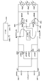
복수의 PV-및-PAMCC 모듈을 포함하는 어레이를 논의하기 전에, 개별적인 PAMCC를 먼저 살펴본다. 예를 들어, 도 4를 참조하면, PV 패널은 도면번호 (401)로 도시된 다이오드 및 커패시터에 의해 전자적으로 대표된다. 전술한 바와 같이, 태양광 패널(401)은 DC 소스로 교체될 수 있다. 총괄적으로, PAMCC(또는 가끔씩 "마이크로 인버터")를 포함하는 컴포넌트는 단순히 "PAMCC(400)"로 언급된다. 전류는 PV(401)에 의해 양의 입력 단자(402) 및 음의 입력 단자(404)로 제공된다. 양의 입력 단자(402)는 코일 L1(406)과 직렬로 연결된다. 음의 입력 단자(404)는 코일 L2(405)와 직렬로 연결된다. 일 실시예에서, 코일 L1(406) 및 L2(405)는 두 개의 입력 단자 및 두 개의 출력 단자를 구비한 일대일 변압기를 형성한다. 이러한 실시예는 두 개의 전류 경로를 통해 보다 나은 전류 매칭을 제공한다. 이하, 우리는 "T1"(407)으로서 단일의 변압기를 언급한다. 예를 들어 NMOS FET인 스위치 Q1(404)은 변압기 T1(407)의 부하측을 가로질러 연결되며, Q1(404)의 소스는 T1(407)의 음극단에 병렬로 연결된다. PV(401) 및 PAMCC(400)의 음극 측이 플로팅 식이며, 다시 말해 이들은 전기적으로 접지되지 않는다. 제어기(412)는 신호를 랄인(411)에서 Q1(404)의 제어 게이트(Q1G)로 제공하는 출력단(414)을 구비한다. 일부 실시예에서, 제어기(412)는 추가적인 로직을 구비한 마이크로프로세서이며, 프로그램에 의해 구동된다. 제어기(412)는 이하 보다 상세하게 기술된다. Before discussing an array that includes multiple PV-and-PAMCC modules, the individual PAMCCs are first discussed. For example, referring to FIG. 4, a PV panel is electronically represented by a diode and capacitor, shown at 401. As mentioned above, the
제어기(412)는 복수의 출력단들을 포함하며, 각각은 독립적으로 구동된다. 네 개의 제어기(412)의 출력 단자들(415 내지 418)은 네 개의 라인들(119 내지 422)에 의해 각각 네 개의 트라이액(각각 CR11(424); CR22(423); CR12(425); 및 CR21(426))의 제어단에 연결된다. 각각의 트라이액에 대해 각각의 라인은 제어기(412)의 제어 신호에 의해 독립적으로 제어된다. CR11(424) 및 CR22(423)의 애노드 단자는 T1(407)의 양의 출력 단자에 병렬로 연결된다. 트라이액 CR12(425) 및 CR21(426)의 캐소드 단자는 T1(407)의 음의 출력 단자에 병렬로 연결된다. 트라이액 CR11(424)의 캐소드 단자 및 트라이액 CR12(425)의 애노드 단자는 코일 L12(430)에 병렬로 연결된다. 트라이액 CR22(423)의 캐소드 단자 및 트라이액 CR21(426)의 애노드 단자는 코일 L22(431)에 병렬로 연결된다. 코일 L12(430)으로부터의 단자(434)는 "위상 1"(P1) 출력을 제공하는 것으로 임의로 지정되고 코일 L22(431)로부터의 단자(436)은 "위상 2"(P2) 출력을 제공하는 것으로 임의로 지정된다. 일부 실시예에서, 코일 L12(430) 및 L22(431)은 일대일 변압기에 구현된다. 도 4에 예시적으로 도시된 실시예에서, 코일 L12(430) 및 L22(136)은 분리된 코일이다. 커패시터 C12(438)는 코일 L12(430)의 입력 측과 중립적인 출력 단자(432)를 가로지른다. 다른 커패시터 C22는 코일 L22(431)의 입력 측과 중립적인 출력 단자(432)를 가로지른다. 다른 실시예에서는 중립적인 출력 단자(432)가 없으며, 코일 L12(430) 및 L22(431)의 입력 단자를 가로지르는 단일의 커패시터가 구비되며; 이 실시예에서, 커패시터의 전압 레이팅은 커패시터 C22(440) 및 C12(438)의 전압 레이팅의 적어도 두 배이다. The
본 발명의 방법은 라인(411 및 419 내지 422)에서의 제어 신호에 의해 구현된다. 특히, 라인(411)에서의 제어 신호 Q1G 및 라인(419)에서의 신호 CR11T; 라인(420)에서의 CR22T; 라인(421)에서의 CR12T; 및 라인(422)에서의 CR21T는, 고주파수 주기, 예를 들어 30 KHz로 PAMCC(400) 내의 시퀀스에서 PV(401)에 의해 제공되는 전류를 연결시키고 차단시키며, 이는 슬로우어(slower)에 의해 변조된 PCM 신호를 60 사이클 패턴으로 제공하여, 진폭이 사인파에 근사한 PAM 신호인 출력을 제공한다. The method of the present invention is implemented by control signals in
도 2를 참조하면, 초기 조건은 다음과 같다: Q1(404), CR11(424), CR22(423), CR12(425) 및 CR21(426)은 에너지가 공급되지 않으며; 코일 L1(406), L2(405), L12(430) 및 L22(431)은 전류가 없으며; 태양광발전 셀 PV1 내지 PVn은 어둡다. 이러한 조건에서, 그리드 AC 전압은 P1(434)과 P2(436) 사이에 인가되며, L12(430), C12(438), C22(440) 및 L22(431)를 통하는 경로를 경험한다. L12(430) 및 C12(438)을 포함하는 재구성 필터를 위해 선택된 공진 주파수는 일반적으로 Q1(404)의 스위칭 주파수의 약 1/2가 되도록 선택된다. L22(431) 및 C22(440)를 포함하는 재구성 필터의 공진 주파수는 L12(430) 및 C12(438)의 재구성 필터의 주파수와 동일하게 선택된다. 일 실시예에서, 트랜지스터 Q1(404)은 약 30 KHz의 명싯된 스위칭 주파수를 위해 선택되고, 그리고 나서 재구성 필터의 공진 주파수는 15 KHz로 설계된다. 일반적으로 60 Hz인 그리드 AC 전압으로, 중요하지 않은 양의 용량성의 반응성 부하는 그리드로 표현된다. Referring to Figure 2, the initial conditions are as follows:
회로의 동작은 태양광 패털(401)이 충분한 전류를 생성하기 위해 충분한 빛에 노출되는 것으로 시작한다. 전류의 존재는 Q1(404)을 가로지르는 전류가 증가함에 따라 관찰될 수 있다. 이 점에서, Q1(404)은 처음에 Q1G와 Q1S 간의 라인(411) 상에서 제어기(412)로부터 신호를 인가함으로써 턴온된다. 제어기(412)와 트랜지스터 Q1(404) 간의 인터페이스는 광학적으로 고립되며, 변압기와 결합되거나, 제어기(412)는 Q1S에 연결될 수 있다. 이러한 상태에서, L1(406) 및 L2(405)는 전류로 충전되기 시작한다. PV(401)를 가로지르는 전압이 기결정된 값으로 감소하는 경우, 코일이 충전되기 위한 시간은 전류를 계산하기 위해 언급되고, 표준 동작이 다음 그리드가 영값을 가로지르면서 시작된다. 일 실시예에서, 이는 P1에서의 전압이 P2 이상으로 가로지르면서 P1이 양의 값을 가지고 P2가 음의 값을 가지는 경우이다. 이 점에서, 신호 CR11T(419) 및 CR21T(421)가 인가되어, 전류가 CR11(424) 및 CR21(426)로 인가되는 경우 이들은 도통될 것이다.
The operation of the circuit begins with the
실시예 1: 그리드의 양의 반파를 위한 PWM 변조Example 1 PWM Modulation for Positive Halfwaves in a Grid
도 5 내지 도 8이 PAMCC(400)의 동작을 기술하도록 참조될 것이다. 컴포넌트들이 도 4의 컴포넌트들에 대응하지만, 설명을 불명확하지 않도록 하기 위해 도면번호가 유지된다. 그러나, 도 4에 제공된 도면번호를 언급하기로 한다. 도 5를 참조하면, L1(406) 및 L2(405)가 충전되면서, Q1(404)은 펄스 폭 변조 시간동안 턴 오프된다. 턴 오프 시간이 경과된 후, Q1(404)은 전류 스위칭 사이클이 끝날 때까지 턴 온된다. Q1(404)이 오프된 시간 동안, L1(406) 및 L2(405)에 이전에 저장된 전류는 PV(401)에서 흐르는 전류와 함께 CR(11)(424) 및 CR21(426)의 입력 단자로 인가되며, 이는 그리드의 전체 양의 반 사이클 동안 신호 CR11T(419) 및 CR21T(421)의 결과로서 인에이블로 유지된다. 그리드의 양의 반 사이클은 조건에 따라 정의되며, 출력 단자 P1(434)에서의 전압은 출력 단자 P2(436)에서의 전압보다 더 크다. 트라이액 CR11(424)를 통해 전달된 전류 펄스의 전하는 초기에 커패시터 C12(438)에 저장되어, 출력 단자 P1(434)에 연결된 코일 L12의 단부에 대하여 코일 L12(430)의 단부 근처에서 보다 양의 값을 가진 전압을 생성한다. 트라이액 CR21(426)을 통해 전달된 전류 펄스의 전하는 초기에 커패시터 C22(440)에 저장되며, 전압은 출력 단자 P2(436)에 연결된 코일 L22의 단부에 대해 코일 L22(431)의 단부 근처에서 보다 음의 값을 가진다. 이는, L12(430), C12(438)을 포함하는 재구성 필터 및 L22(431), C22(440)을 포함하는 재구성 필터 둘 모두에 대한 초기 조건이다. 이 점에서, 도 5에 도시된 바와 같이, 재구성 필터는 이들에게 전달된 펄스 폭 변조된 전류 펄스를 그리드로 전달되는 전류(505)의 PAM(pulse amplitude modulated) 반 사인파로 변환할 것이다. 5-8 will be referred to to describe the operation of the
재구성 필터를 위한 공진 주파수는 Q1(404)의 스위칭 주파수의 약 1/2가 되도록 선택되어, 사인파 전류의 절반은 P1(434) 및 P2(436)으로 전달된 각각의 펄스 폭 변조된 전류 펄스를 위해 P1(434) 및 P2(436)으로 제공될 것이다. 각각의 재구성 필터의 공진 주파수가 이들에게 인가된 전류의 펄스 폭에 독립적이고, 재구성 필터로 인가되는 순간 전류 펄스의 전하가 재구성 필터를 벗어나 그리드로 전달되는 반 사인파의 전류의 전하와 동일해야 하므로, 입력 전류의 펄스 폭에 대한 변화은 재구성 필터의 출력의 진폭에 대한 변화로 반영될 것이다. 재구성 필터 내의 인덕터의 전류가 영으로 되돌아감에 따라, 다음 펄스의 전류는 재구성 필터의 커패시터로 전달되며, 이는 재구성 필터의 주파수가 펄스 폭 변조된 전류 펄스가 Q1(404)에 의해 생성되는 레이트의 절반이기 때문이다. The resonant frequency for the reconstruction filter is chosen to be about one half of the switching frequency of
Q1(404)의 오프 시간은 변조되어 생성된 전류 펄스의 폭은 그리드 사인파의 형상 내에 위치한다. 재구성 필터는 이러한 펄스 폭 변조된 전류 펄스의 시퀀스를, 진폭이 그리드 사인파의 형상의 대응되는 지점을 뒤따르는 펄스 진폭 변조된 전류 펄스의 시퀀스로 변환된다. The off time of
그리드 반 사이클이 단자 P2(436)의 출력에 대해 단자 P1(434)에서 양의 값으로 유지되는 한, 추가적인 전류 펄스가 "실시예 1: 그리드의 양의 반파를 위한 PWM 변조"에서 시작하는 전술된 프로세스를 반복함으로써 생성된다. As long as the grid half cycle remains positive at
음의 값을 갖는 영을 가로지르는 그리드 전압은, P1(434)이 P2(436)보다 더 양의 값을 갖게 된 후 단자 P1(434)에서의 전압이 단자 P2(436)에서의 전압과 동일하게 되는 조건으로 정의된다. 음의 갑승로 영을 가로지르기 전에, Q1(404)은 턴 온되어, 전류를 CR11(424) 및 CR21(426)으로부터 제거한다. 이 점에서, 신호 CR11T(419) 및 CR21T(421)은 차단되어, 그리드가 음의 반사이클인 도중 트라이액 CR11(424) 및 CR21(426)이 전류를 전달하는 것을 방지한다. 음의 값으로 영을 가로지른 후, 단자 P1(434)의 전압이 단자 P2(436)의 전압보다 더 음의 값을 가지면서, 신호 CR22T(420) 및 CR12T(421)이 인가되어, 전류가 CR22(423) 및 CR12(425)으로 인가되면 이들이 도전되도록 한다.
The grid voltage across zero having a negative value is equal to the voltage at
실시예 2: 그리드의 음의 반파를 위한 PWM 변조Example 2: PWM Modulation for Negative Half Wave of Grid
도 6을 참조하면, L1(406) 및 L2(405)가 Q1이 충전되면서, Q1(404)은 펄스 폭 변조 시간 동안 턴 오프된다. 오프 시간이 경과된 후, Q1(404)은 순간 전류 스위칭 사이클이 끝날 때까지 턴 온된다. Q1(404)이 오프되는 시간 동안, PV(401)를 흐르는 전류와 함께 L1(406) 및 L2(405)에 기저장된 전류는, 그리드의 전체 음의 반 사이클 동안 신호 CR22T(420) 및 CR12T(421)에 의해 인에이블되도록 유지되는 CR12(425) 및 CR22(423)의 입력 단자에 인가된다. 그리드의 음의 반 사이클은, 단자 P1(434)에서의 전압이 단자 P2(436)에서의 전압보다 더 큰 조건으로 정의된다. 트라이액 CR22(423)을 통해 전달되는 전류 펄스의 전하는 초기에 커패시터 C22(440)에 저장되어, 단자 P2(436)에 연결된 단부에 대하여 코일 L22(431)의 단부 근처에서 보다 양의 값을 갖는 전압을 생성한다. CR12(425)를 통해 전달되는 전류 펄스의 전하는 초기에 C12에 저장되며, 전압은 단자 P1(434)에 연결된 단부에 대하여 코일 L12(430)의 단부 근처에서 보다 양의 값을 갖게 된다. 이는 L12(430), C12(438)을 포함하는 재구성 필터 및 L22(431), C22(440)을 포함하는 재구성 필터 둘 모두에 대한 초기 조건이다. 이 점에서, 도 4에 도시된 바와 같이, 재구성 필터는 이들에게 전달된 펄스 폭 변조된 전류 펄스를 그리드로 전달되는 펄스 폭 변조된 반 사인파의 전류로 변환할 것이다. Referring to FIG. 6, as
실시예 2를 위한 재구성 필터는 실시예 1과 관련되어 기술된 컴포넌트와 동일하며; 그 설계 및 동작은 여기에서 반복되지 않는다. The reconstruction filter for Embodiment 2 is identical to the component described in connection with
Q1(404)의 오프 시간은 변조되어, 생성된 전류 펄스의 폭은 그리드 사인파의 형상 내에 위치한다. 재구성 필터는 이러한 펄스 폭 변조된 전류 펄스의 시퀀스를, 진폭이 그리드 사인파의 형상의 대응되는 지점을 뒤따르는 펄스 진폭 변조된 전류 펄스의 시퀀스로 변환한다. The off time of
그리드의 반 사이클이 음의 값으로 유지되는 한, 단자 P1(434)의 전압이 단자 P2(436)의 전압보다 더 음의 값을 가지면서, 추가적인 전류 펄스는, "실시예 2: 그리드의 음의 반파를 위한 PWM 모듈"에서 시작하는 전술된 프로세스를 반복함으로써 생성된다. As long as the half cycle of the grid remains negative, while the voltage at
그리드 전압의 양의 값으로 영을 가로지르는 것은, 단자 P1(434)에서의 전압이 단자 P2(436)의 전압보다 더 음의 값을 갖게된 후 단자 P1(434)에서의 전압이 P2(436)과 동일한 조건으로 정의된다. 양의 값으로 영을 가로지르기 전에, Q1(404)은 턴 온되어, 전류를 트라이액 CR12(425) 및 CR22(423)으로부터 제거한다. 이 점에서, 신호 CR12T(421) 및 CR22T(420)은 차단되어, 트라이액 CR12(425) 및 CR22(423)이 그리드의 양의 반 사이클 도중 전류를 전달하는 것을 방지한다. P1(434)이 P2(436)보다 더 양의 값을 가지면서 양의 값으로 영을 가로지른 후, 신호 CR11T(419) 및 CR21T(421)은 인가되어, 전류가 트라이액 CR11(424) 및 CR21(426)으로 인가되는 경우 트라이액 CR11(424) 및 CR21(426)이 도전되도록 한다. Crossing zero with a positive value of the grid voltage means that the voltage at
그리드가 다시 양의 값으로 되면서, 프로세스는 다시 전술된 프로세스로 되돌아가, 실시예 1: 그리드의 양의 반 파를 위한 PWM 변조 섹션에서 시작된다. As the grid becomes positive again, the process goes back to the process described above, and starts with Example 1: PWM modulation section for positive half wave of the grid.
도 9는 재구성 필터, 예컨대 전술된 (L12(430) 및 C12(438); L22(431) 및 C22(440))에 의해 펄스 진폭 변조된(PAM) 전류 펄스로 변환되는, 펄스 폭 변조된 펄스의 변환 결과의 신호도를 도시한다. 짧은 듀레이션의 대략적으로 사각형의 전압 펄스(902)는 Q1(404)의 드레인 측(451)(도 4)에서의 전압이다. 펄스 폭(908)은 라인(411)에서의 신호 Q1G의 펄스 폭과 근사하고(도 4), 주기(910)는 PAMCC(400)의 스위칭 주기이다. 이러한 전압은 트라이액 CR11(424) 또는 CR12(425)를 통해(전술한 바와 같이, 제어기(412)로부터의 제어 신호의 순간 상태에 따라) 재구성 필터 중 어느 하나의 입력으로 변압기(407) 및 PV(401) 전류를 인가한다. 만곡된 반파정류된 사인파(904)는 재구성 필터의 출력이다. 입력 펄스의 펄스 폭(908)(근사적으로)이 증가함에 따라, 출력 파형(904)의 진폭은 증가한다. 그래프의 상부의 삼각파형(906)은 공통된 시간 창 도중 PV(401)를 통하는 전류의 변화를 그린다. 트레이스(906)는 상대적으로 일정한 PV(401) 전류를 유지하는 변압기(407)의 효과를 도시하며, 이는 재구성 필터로 제공되는 상대적으로 큰 펄스 폭 변조된 전류 펄스에 독립적이다. 9 shows a pulse width modulated pulse, which is converted into a pulse amplitude modulated (PAM) current pulse by a reconstruction filter, such as (
도 10은 도 11, 도 12 및 도 13에 도시될 그리드 사인파 사이클의 좁은 타임 슬라이스를 도시한다. FIG. 10 shows a narrow time slice of the grid sine wave cycle to be shown in FIGS. 11, 12 and 13.
도 11은 단일의 PAMCC(400)의 펄스 진폭 변조된 출력 전류를 도시한다. 도시된 진폭은 사이클 예(1101)에 도시된 그리드 전압의 양의 피크값 근처의 시간 중 작은 부분에 대한 것이다. 개별적인 펄스(1104)는 스위칭 주파수, 예컨대 1/30 KHz의 주기와 동일한 주기(1106)를 가진다. 11 illustrates pulse amplitude modulated output current of a
도 12에서, 두 개의 PAMCC들(각각은 PAMCC(400)에 따름)의 두 개의 개별적인 전류(1200.1 및 1200.2)는 스위칭 주파수의 주기의 절반으로 이위상된다. 위의 트레이스(1202)는 두 PAMCC 출력 전류들(1200.1 및 1200.2)의 합이다. 합산된 전류(1202)가 단일 PAMCC(도 11 참조)의 리플보다 훨씬 더 작은 리플을 가지며 단일의 인버터의 리플 주파수의 두 배의 리플 주파수를 갖는다. 합산된 전류(1202)는 영으로 되지 않는다. In FIG. 12, two separate currents 1200.1 and 1200.2 of two PAMCCs (each according to PAMCC 400) are out of phase with half the period of the switching frequency. The
두 개의 PAMCC(400) 출력 전류의 합에 뒤이어, 도 13은 여덟 개의 PAMCC의 개별적인 출력 전류들을 도시하며(라인(1300)은 대표적인 것이며; 각각의 파형은 번호가 매겨지지 않음), 각각은 스위칭 주파수의 주기를 걸쳐 균등하게 위상이 분포한다. 예를 들어, 30 KHz의 스위칭 주파수를 사용하는 시스템에 대하여, 주기는 33.3 마이크로초이고, 각각의 위상은 이전 출력 전류 파형에 대하여 33.3/8 또는 4.167 마이크로초만큼 지연된다. 임의의 개수의 PAMCC(400)는 이와 같이 합산될 수 있다. 합산된 개수가 증가함에 따라, 이들은 더 작은 수에 의해 위상 지연되며(1/(스위칭 주파수)*n), 여기서 "n"은 합산된 PAMCC의 개수이다. 도 13에 도시된 합산된 전류가 개별적인 PAMCC의 리플 전류의 일부만을 가지며 개별적인 PAMCC의 리플 주파수의 8배에 해당되는 리플 주파수를 갖는다. 각각의 PAMCC(400)가 PAM 전류 펄스의 시퀀스와 함께 그리드 사인파 상의 지점을 생성하는 경우, 한 세트의 PAMCC를 이위상하고 합산하며, 컨버터의 어레이를 형성하는 것은, 매우 높은 정확도 및 매우 낮은 노이즈(리플)로 그리드 사인파의 전류를 효과적으로 복조할 것이다. 임의의 개수의 어레이 컨버터는 이러한 방식으로 이위상되고 합산될 수 있다. PAMCC의 수가 증가함에 따라, 리플 진폭은 감소하고 리플 주파수는 증가한다. 일 실시예에서, 복수의 PAMCC(400) 중 둘 또는 그 이상의 개별적인 출력 전류는 서로 간에 동위상된다(in phase). 일부 실시예에서, 스위칭 주파수는 그리드 주파수, 예를 들어 미국에서의 60 Hz와 관련되지 않도록 선택되며, 리플은 조화 왜곡을 나타내지 않을 것이다. PAMCC 출력으로 변조된 신호는 임의적이다. 일부 실시예에서, 다수의 신호는 PAMCC 출력으로 변조되며, 이러한 신호 중 하나는, 예를 들어 임의적인 둘 또는 그 이상의 PAMCC 모듈 간의 통신을 제공한다. PAMCC 변조는 가끔씩 그리드 신호의 왜곡을 수집하도록 사용된다. Following the sum of the two
어레이로 구성된 PAMCC(400)의 위상형성을 선택하는 다수의 방법 중 하나는, 각각의 PAMCC(400)가 타이밍 슬랏 번호를 미리-할당받으며, 제 1 슬랏이 영을 가로지른 후 스케쥴링되고 각각의 PAMCC(400)가 그 PAM 신호를 기결정된(즉, 할당된) 시퀀스로 제공한다. One of a number of methods for selecting the phase formation of an array of
대안적인 실시예에서, 도 14에 예시적으로 도시된 바와 같이, 제 2 트랜지스터가 추가되며, Q1A(1402) 및 Q1B(1404)가 도 4의 회로에 도시되고 기술된 바와 같은 단일 트랜지스터 Q1(404)를 대체한다. 두 개의 트랜지스터 Q1A(1402) 및 Q1B(1404)를 사용하는 것은 일부 잠재적인 장점을 제공하며, 이는 각각의 트랜지스터를 가로지르는 전압을 감소시키고, Q1(404)의 Rds_on 요건에 비해 각각의 트랜지스터에 대해 보다 완화된 Rds_on("온"으로 된 저항) 요건을 허용하며, 각각의 트랜지스터가 상대적으로 낮은 전압과 PV(401)의 안정된 애노드 및 캐소드 단부에 대하여 구동되도록 한다. 이러한 구성에서, Q1A(1402) 및 Q1B(1404)는 전술된 Q1(404)와 동일한 시간에 턴 온되고 턴 오프된다. 회로 동작의 다른 모든 양태는 도일하게 유지된다. Q1A(1402) 및 Q1B(1404)가 서로 다른 트랜지스터 타입이므로, 제어(1412)에 의해 이들의 제어 게이트로 개별적인 신호가 제공된다. 그렇지 않으면, 각각 라인(1401 및 1403)을 통해 Q1A(1402) 및 Q1B(1404)의 제어 게이트로 연결되는 출력 단자가 추가되면서, 제어기(1412)는 도 12의 제어기(412)와 동일하다. In an alternate embodiment, as illustrated by way of example in FIG. 14, a second transistor is added, and
일부 실시예에서, 시스템은 안전성, 유지보수 또는 다른 목적을 위해 셧다운될 수 있다. 셧-다운 방법의 일 예는 도 15에 도시된다. 트랜지스터 TR1(1502) 및 릴레이 S1(1504)가 도시된 바와 같이 추가된다. 이러한 예는 두 개의 트랜지스터 Q1A(1402) 및 Q1B(1404)를 포함하지만, 동일한 셧-다운 제공이 도 4의 회로에도 추가될 수 있으며, 두 개의 트랜지스터 Q1A 및 Q1B는 단일 트랜지스터 Q1(404)에 의해 대체된다. 트랜지스터 TR1(1502) 및 릴레이 S1(1504)는 PAMCC의 안전한 셧다운을 제공하면서 빛을 받으며 전력을 생성하는 PV(401)로 연결시킨다. 셧다운 프로세스는 제어기(1512)로부터 라인(1506)에 신호 TR1B를 제공함으로써 개시되며, 라인(1506)은 트랜지스터(1502)의 제어 게이트에 연결된다. 트랜지스터 TR1(1502)가 턴 온되면, TR1은 PV(401)에 의해 생성된 전류를 위해 짧은 경로를 형성하며, 이는 PV(401)를가로지르는 전압이 작은 수준으로 감소되도록 유발한다. 이 점에서, Q1A(1402) 및 Q1C(1404)는 코일 L1(406) 및 L2(405)의 전류가 낮은 수준으로 감소하도록 에너지가 제공된다. 코일 L1 및 L2가 방전된 후, 릴레이 S1(1504)은 개방된다. 그리드로의 경로가 이제 개방되면서, Q1A(1402) 및 Q1B(1404)는 턴 오프되며, 뒤이어 트랜지스터 TR1(1502)가 턴 오프된다. 이러한 구성에서, 어떠한 추가적인 전력도 생성되지 않을 것이다. In some embodiments, the system can be shut down for safety, maintenance, or other purposes. One example of a shut-down method is shown in FIG. 15.
도 16은 본 발명을 구현하기 위한 또 다른 대안적인 토폴로지를 도시한다. DC 소스(1602)는 라인(1610)의 버스에서 복수의 PAMCC(1604.1, 1604.n) 유닛들로 전류를 제공한다. DC 소스(1602)는 임의의 다양한 DC 전류원, 예를 들어 배터리, 병렬로 연결된 다수의 배터리들(병렬로 연결된 배터리 중 일부는 직렬로 연결된 배터리에 의해 형성될 수 있음), 또는 AC 라인 소스로부터 DC 전류를 제공하는 전원이다. 전술한 바와 같이, PAMCC(11604.1, 1604.n)의 전류 출력은 버스(1612)에서 이위상되어 합산되어 부하(1606)로 AC 전력을 제공한다. 부하(1606)는 외부 그리드일 수 있다. Figure 16 illustrates another alternative topology for implementing the present invention.
1602: DC 소스 1604.1 내지 1504.n: PAMCC
1606: 부하 1610: 라인
1612: 버스1602: DC source 1604.1 to 1504.n: PAMCC
1606: load 1610: line
1612: bus
Claims (40)
둘 또는 그 이상의 직류 전류원;
각각의 직류 전류원에 연결된 PAMCC(pulse ampllitude modulated current converter)("컨버터")를 포함하며,
각각의 컨버터는 각각의 직류 전류원으로부터 직류 전류를 받고, 상기 컨버터의 출력 단자에서 펄스 진폭 변조된 전류 펄스(pulse amplitude modulated current pulses)를 제공하며, 각각의 컨버터의 출력 단자는 시스템 내 다른 모든 컨버터들의 출력 단자와 전기적으로 병렬 연결되며, 적어도 두 개의 컨버터들의 전류 펄스는 서로에 대해 이위상되어(out of phase), 모든 컨버터들의 전류 펄스를 합하여 상기 컨버터들의 펄스 출력에 변조된 신호가 복조되는 것을 특징으로 하는 전력 변환 시스템.In a system for converting power,
Two or more direct current sources;
Includes a pulse ampllitude modulated current converter (PAMCC) ("converter") connected to each direct current source,
Each converter receives direct current from a respective direct current source and provides pulse amplitude modulated current pulses at the output terminal of the converter, the output terminal of each converter being connected to all other converters in the system. Electrically connected in parallel with the output terminals, wherein the current pulses of at least two converters are out of phase with respect to each other so that the current pulses of all the converters are summed to demodulate the modulated signal at the pulse outputs of the converters. Power conversion system.
각각의 컨버터의 전류 펄스는 다른 모든 컨버터들의 전류 펄스에 대하여 이위상되는 것을 특징으로 하는 전력 변환 시스템.The method of claim 1,
The current pulse of each converter is out of phase with respect to the current pulses of all other converters.
상기 신호는 60-사이클의 교류 전류 전압인 것을 특징으로 하는 전력 변환 시스템.The method of claim 1,
The signal is a 60-cycle alternating current voltage.
상기 신호는 대략적으로 고정된 값의 직류 전류 전압인 것을 특징으로 하는 전력 변환 시스템.The method of claim 1,
And the signal is a approximately fixed value of direct current voltage.
상기 신호는 방형파인 것을 특징으로 하는 전력 변환 시스템.The method of claim 1,
And the signal is a square wave.
상기 신호는 삼각파인 것을 특징으로 하는 전력 변환 시스템.The method of claim 1,
And the signal is a triangular wave.
상기 신호는 가우시안 파(Gaussian wave)인 것을 특징으로 하는 전력 변환 시스템.The method of claim 1,
And the signal is a Gaussian wave.
상기 신호는 데이터를 통신하도록 통신 신호를 제공하는 것을 특징으로 하는 전력 변환 시스템.The method of claim 1,
And the signal provides a communication signal to communicate data.
상기 통신 신호는 주어진 컨버터로부터 상기 시스템 내 적어도 하나의 다른 컨버터로 데이터를 제공하는 것을 특징으로 하는 전력 변환 시스템.The method of claim 8,
The communication signal provides data from a given converter to at least one other converter in the system.
상기 통신 신호는 주어진 컨버터로부터 상기 시스템 내 다른 모든 컨버터들로 데이터를 제공하는 것을 특징으로 하는 전력 변환 시스템.The method of claim 8,
The communication signal provides data from a given converter to all other converters in the system.
상기 데이터는 위상 데이터를 포함하는 것을 특징으로 하는 전력 변환 시스템.The method of claim 8,
And the data comprises phase data.
상기 데이터는 제어 명령을 포함하는 것을 특징으로 하는 전력 변환 시스템.The method of claim 8,
And the data includes a control command.
상기 데이터는 동작 데이터를 포함하는 것을 특징으로 하는 전력 변환 시스템.The method of claim 8,
And the data includes operational data.
상기 둘 또는 그 이상의 직류 전류원은 태양광발전 패널인 것을 특징으로 하는 전력 변환 시스템.The method of claim 1,
And said at least two direct current sources are photovoltaic panels.
상기 둘 또는 그 이상의 직류 전류원은 풍력 발전기인 것을 특징으로 하는 전력 변환 시스템.The method of claim 1,
And the two or more direct current sources are wind generators.
상기 둘 또는 그 이상의 직류 전류원은 조력 발전기인 것을 특징으로 하는 전력 변환 시스템.The method of claim 1,
And the two or more direct current sources are tidal generators.
상기 둘 또는 그 이상의 직류 전류원은 압전(piezoelectric) 발전기인 것을 특징으로 하는 전력 변환 시스템.The method of claim 1,
And the two or more direct current sources are piezoelectric generators.
상기 둘 또는 그 이상의 직류 전류원은 배터리인 것을 특징으로 하는 전력 변환 시스템.The method of claim 1,
And said at least two direct current sources are batteries.
상기 통신 신호는 상기 신호 상에서 중첩되는 것을 특징으로 하는 전력 변환 시스템.The method of claim 8,
The communication signal is superimposed on the signal.
상기 전류 펄스는 상기 신호의 임의의 왜곡을 감소시키도록 변형되는 것을 특징으로 하는 전력 변환 시스템.The method of claim 1,
And the current pulse is modified to reduce any distortion of the signal.
직류 전류원;
상기 직류 전류원에 연결된 복수의 PAMCC("컨버터")를 포함하며,
각각의 컨버터는 상기 직류 전류원으로부터 직류 전류를 받고, 각각의 컨버터는 상기 컨버터의 출력 단자에서 펄스 진폭 변조된 전류 펄스를 제공하며, 각각의 컨버터의 출력 단자는 상기 시스템 내 다른 모든 컨버터들의 출력 단자와 전기적으로 병렬 연결되며, 적어도 두 개의 컨버터들의 전류 펄스는 서로에 대해 이위상되어, 모든 컨버터들의 전류 펄스를 합하여 상기 컨버터의 펄스 출력에 변조된 신호가 복조되는 것을 특징으로 하는 전력 변환 시스템.In a system for converting power,
DC current source;
A plurality of PAMCCs ("converters") connected to said direct current source;
Each converter receives a direct current from the direct current source, each converter provides a pulse amplitude modulated current pulse at the output terminal of the converter, the output terminal of each converter being coupled with the output terminals of all other converters in the system. And electrically connected in parallel, wherein the current pulses of at least two converters are out of phase with respect to each other such that the current pulses of all the converters are summed to demodulate the modulated signal at the pulse output of the converter.
각각의 컨버터의 전류 펄스는 다른 모든 컨버터들의 전류 펄스에 대하여 이위상되는 것을 특징으로 하는 전력 변환 시스템.The method of claim 21,
The current pulse of each converter is out of phase with respect to the current pulses of all other converters.
상기 신호는 60-사이클의 교류 전류 전압인 것을 특징으로 하는 전력 변환 시스템.The method of claim 21,
The signal is a 60-cycle alternating current voltage.
상기 신호는 대략적으로 고정된 값의 직류 전류 전압인 것을 특징으로 하는 전력 변환 시스템.The method of claim 21,
And the signal is a approximately fixed value of direct current voltage.
상기 신호는 방형파인 것을 특징으로 하는 전력 변환 시스템.The method of claim 21,
And the signal is a square wave.
상기 신호는 삼각파인 것을 특징으로 하는 전력 변환 시스템.The method of claim 21,
And the signal is a triangular wave.
상기 신호는 가우시안 파(Gaussian wave)인 것을 특징으로 하는 전력 변환 시스템.The method of claim 21,
And the signal is a Gaussian wave.
상기 신호는 데이터를 통신하도록 통신 신호를 제공하는 것을 특징으로 하는 전력 변환 시스템.The method of claim 21,
And the signal provides a communication signal to communicate data.
상기 통신 신호는 주어진 컨버터로부터 상기 시스템 내 적어도 하나의 다른 컨버터로 데이터를 제공하는 것을 특징으로 하는 전력 변환 시스템.The method of claim 28,
The communication signal provides data from a given converter to at least one other converter in the system.
상기 통신 신호는 주어진 컨버터로부터 상기 시스템 내 다른 모든 컨버터들로 데이터를 제공하는 것을 특징으로 하는 전력 변환 시스템.The method of claim 28,
The communication signal provides data from a given converter to all other converters in the system.
상기 데이터는 위상 데이터를 포함하는 것을 특징으로 하는 전력 변환 시스템.The method of claim 28,
And the data comprises phase data.
상기 데이터는 제어 명령을 포함하는 것을 특징으로 하는 전력 변환 시스템.The method of claim 28,
And the data includes a control command.
상기 데이터는 동작 데이터를 포함하는 것을 특징으로 하는 전력 변환 시스템.The method of claim 28,
And the data includes operational data.
상기 둘 또는 그 이상의 직류 전류원은 태양광발전 패널인 것을 특징으로 하는 전력 변환 시스템.The method of claim 21,
And said at least two direct current sources are photovoltaic panels.
상기 둘 또는 그 이상의 직류 전류원은 풍력 발전기인 것을 특징으로 하는 전력 변환 시스템.The method of claim 21,
And the two or more direct current sources are wind generators.
상기 둘 또는 그 이상의 직류 전류원은 조력 발전기인 것을 특징으로 하는 전력 변환 시스템.The method of claim 21,
And the two or more direct current sources are tidal generators.
상기 둘 또는 그 이상의 직류 전류원은 압전(piezoelectric) 발전기인 것을 특징으로 하는 전력 변환 시스템.The method of claim 21,
And the two or more direct current sources are piezoelectric generators.
상기 둘 또는 그 이상의 직류 전류원은 배터리인 것을 특징으로 하는 전력 변환 시스템.The method of claim 21,
And said at least two direct current sources are batteries.
상기 통신 신호는 상기 신호 상에서 중첩되는 것을 특징으로 하는 전력 변환 시스템.The method of claim 28,
The communication signal is superimposed on the signal.
상기 전류 펄스는 상기 신호의 임의의 왜곡을 감소시키도록 변형되는 것을 특징으로 하는 전력 변환 시스템.The method of claim 21,
And the current pulse is modified to reduce any distortion of the signal.
Applications Claiming Priority (4)
| Application Number | Priority Date | Filing Date | Title |
|---|---|---|---|
| US12/061,025 | 2008-04-02 | ||
| US12/061,025 US7719864B2 (en) | 2008-04-02 | 2008-04-02 | Pulse amplitude modulated current converter |
| US12/276,411 US7929324B1 (en) | 2008-04-02 | 2008-11-23 | Blade architecture array converter |
| US12/276,411 | 2008-11-23 |
Publications (1)
| Publication Number | Publication Date |
|---|---|
| KR20110005834A true KR20110005834A (en) | 2011-01-19 |
Family
ID=41136115
Family Applications (1)
| Application Number | Title | Priority Date | Filing Date |
|---|---|---|---|
| KR1020107024596A KR20110005834A (en) | 2008-04-02 | 2009-04-02 | Blade architecture array converter |
Country Status (9)
| Country | Link |
|---|---|
| US (1) | US7929324B1 (en) |
| EP (1) | EP2272164A2 (en) |
| JP (1) | JP2011517269A (en) |
| KR (1) | KR20110005834A (en) |
| CN (1) | CN102047557A (en) |
| BR (1) | BRPI0906546A2 (en) |
| MX (1) | MX2010010868A (en) |
| TW (1) | TW200950300A (en) |
| WO (1) | WO2009124221A2 (en) |
Families Citing this family (8)
| Publication number | Priority date | Publication date | Assignee | Title |
|---|---|---|---|---|
| US20100301676A1 (en) * | 2009-05-28 | 2010-12-02 | General Electric Company | Solar power generation system including weatherable units including photovoltaic modules and isolated power converters |
| US8467200B2 (en) * | 2010-04-26 | 2013-06-18 | Queen's University At Kingston | Power converter for a power generator |
| JP5928736B2 (en) * | 2010-08-31 | 2016-06-01 | エスエムエー ソーラー テクノロジー アーゲー | Inverter with AC interface for AC module connection |
| US8774974B2 (en) * | 2011-07-15 | 2014-07-08 | First Solar, Inc. | Real-time photovoltaic power plant control system |
| US9234506B2 (en) * | 2011-10-14 | 2016-01-12 | Vestas Wind Systems A/S | Estimation of wind properties using a light detection and ranging device |
| WO2013112981A1 (en) | 2012-01-26 | 2013-08-01 | Cameron D Kevin | Circuit for transferring power between a direct current line and an alternating-current line |
| US20150108851A1 (en) * | 2013-10-19 | 2015-04-23 | UltraSolar Technology, Inc. | Photovoltaic systems with shaped high frequency electric pulses |
| US9496710B2 (en) * | 2014-12-29 | 2016-11-15 | Solarcity Corporation | Rapid shutdown solid state circuit for photovoltaic energy generation systems |
Family Cites Families (17)
| Publication number | Priority date | Publication date | Assignee | Title |
|---|---|---|---|---|
| US4719550A (en) | 1986-09-11 | 1988-01-12 | Liebert Corporation | Uninterruptible power supply with energy conversion and enhancement |
| US5677833A (en) * | 1995-05-16 | 1997-10-14 | Raytheon Company | Power conditioning system for a four quadrant photovoltaic array with an inverter for each array quadrant |
| US5642275A (en) * | 1995-09-14 | 1997-06-24 | Lockheed Martin Energy System, Inc. | Multilevel cascade voltage source inverter with seperate DC sources |
| JP3697121B2 (en) * | 1998-10-15 | 2005-09-21 | キヤノン株式会社 | Photovoltaic power generation apparatus and control method thereof |
| US6603619B1 (en) * | 1999-01-07 | 2003-08-05 | Sharp Kabushiki Kaisha | Magnetic storage medium and heat assisted recording and reproduction method |
| US6198314B1 (en) * | 1999-01-25 | 2001-03-06 | Motorola Inc. | Sample and hold circuit and method therefor |
| RU2218075C2 (en) | 2001-01-09 | 2003-12-10 | Наумов Валерий Аркадьевич | Method and device for recording and processing plethysmogram data to measure human cardiovascular system parameters |
| FR2855677B1 (en) * | 2003-05-30 | 2016-11-04 | Valeo Equip Electr Moteur | PULSE WIDTH MODULATION CONTROL CIRCUIT FOR MULTI MODE ELECTRIC MACHINE AND MULTI MODE ELECTRIC MACHINE EQUIPPED WITH SUCH A CONTROL CIRCUIT |
| US6969967B2 (en) * | 2003-12-12 | 2005-11-29 | Ut-Battelle Llc | Multi-level dc bus inverter for providing sinusoidal and PWM electrical machine voltages |
| US20050139259A1 (en) * | 2003-12-30 | 2005-06-30 | Robert Steigerwald | Transformerless power conversion in an inverter for a photovoltaic system |
| JP4884665B2 (en) * | 2004-11-12 | 2012-02-29 | ローム株式会社 | DC-AC converter, its controller IC, and DC-AC converter parallel operation system |
| DE102004060698B3 (en) * | 2004-12-16 | 2006-06-14 | Infineon Technologies Ag | Polar modulator for use in communication system, has filter provided downstream of output of pulse width modulator, for suppressing harmonic portions of fundamental value of signal measurable at output |
| CN1980033A (en) * | 2005-11-30 | 2007-06-13 | 硕颉科技股份有限公司 | DC./ac. convertion driving circuit |
| US7515019B2 (en) | 2005-12-20 | 2009-04-07 | Honeywell International Inc. | Non-contact position sensor with sonic waveguide |
| US7893346B2 (en) * | 2006-09-28 | 2011-02-22 | Jack Nachamkin | Integrated voltaic energy system |
| US7719864B2 (en) * | 2008-04-02 | 2010-05-18 | Array Converter, Inc. | Pulse amplitude modulated current converter |
| WO2009132158A1 (en) * | 2008-04-22 | 2009-10-29 | Array Converter, Inc. | High voltage array converter |
-
2008
- 2008-11-23 US US12/276,411 patent/US7929324B1/en not_active Expired - Fee Related
-
2009
- 2009-04-02 MX MX2010010868A patent/MX2010010868A/en unknown
- 2009-04-02 JP JP2011503188A patent/JP2011517269A/en active Pending
- 2009-04-02 CN CN2009801203053A patent/CN102047557A/en active Pending
- 2009-04-02 BR BRPI0906546-6A patent/BRPI0906546A2/en not_active IP Right Cessation
- 2009-04-02 TW TW98111049A patent/TW200950300A/en unknown
- 2009-04-02 WO PCT/US2009/039368 patent/WO2009124221A2/en active Application Filing
- 2009-04-02 EP EP20090726777 patent/EP2272164A2/en not_active Withdrawn
- 2009-04-02 KR KR1020107024596A patent/KR20110005834A/en not_active Application Discontinuation
Also Published As
| Publication number | Publication date |
|---|---|
| EP2272164A2 (en) | 2011-01-12 |
| JP2011517269A (en) | 2011-05-26 |
| WO2009124221A2 (en) | 2009-10-08 |
| BRPI0906546A2 (en) | 2015-07-07 |
| TW200950300A (en) | 2009-12-01 |
| MX2010010868A (en) | 2010-12-17 |
| WO2009124221A3 (en) | 2010-01-14 |
| CN102047557A (en) | 2011-05-04 |
| US7929324B1 (en) | 2011-04-19 |
Similar Documents
| Publication | Publication Date | Title |
|---|---|---|
| US7719864B2 (en) | Pulse amplitude modulated current converter | |
| US8093754B2 (en) | High voltage array converter | |
| US7969757B2 (en) | Apparatus providing bias to solar cells | |
| KR20110005834A (en) | Blade architecture array converter | |
| KR101247411B1 (en) | Photovoltaic power plant having an offset voltage source controlling the dc potential at the inverter output | |
| Moonem et al. | Control and configuration of three-level dual-active bridge DC-DC converter as a front-end interface for photovoltaic system | |
| US8482156B2 (en) | Three phase power generation from a plurality of direct current sources | |
| KR20170046990A (en) | Power supply device, and power supply system including the same | |
| Yadav et al. | Analysis and integration of nine level cascaded H-bridge multilevel inverter configuration in a photovoltaic system | |
| US9548610B2 (en) | Control method for arranging DC/AC converters in parallel | |
| Badhoutiya et al. | Boost control for PV applications using impedance source inverter | |
| Ansari et al. | Low-voltage ride-through capability of flyback inverter under BCM operation for AC module applications | |
| Venkatesan et al. | A survey of single phase grid connected photovoltaic system | |
| KR101278533B1 (en) | Module intergrated power regulator system | |
| Kar et al. | Analysis of a five level reduced switch mli for pv pump application in india | |
| Karunamoorthy et al. | A photovoltaic generation system based on Hybrid Multilevel inverter in order to reduce switching for DC micro grids. | |
| Das et al. | SINGLE-PHASE H6 TRANSFORMERLESS INVERTER WITH A SIMPLE BOOST CONVERTER FOR PV-GRID TIED POWER SYSTEMS | |
| Ganesan et al. | An Overview of the PV System | |
| Repak et al. | Design of power converter for model of photovoltaic power plant | |
| Esfandiari et al. | High-resolution numeral-based multilevel inverter with low number of conducting switches for low-voltage PV applications | |
| Kishore et al. | THD Reduction in Renewable Energy System with Multilevel Inverter | |
| Shahid et al. | Single-phase inverter for small voltage supplies for use in distributed measurement systems | |
| WO2011139674A2 (en) | Renewable energy collection and distribution system |
Legal Events
| Date | Code | Title | Description |
|---|---|---|---|
| WITN | Application deemed withdrawn, e.g. because no request for examination was filed or no examination fee was paid |