JP2011517269A - Blade structure array converter - Google Patents
Blade structure array converter Download PDFInfo
- Publication number
- JP2011517269A JP2011517269A JP2011503188A JP2011503188A JP2011517269A JP 2011517269 A JP2011517269 A JP 2011517269A JP 2011503188 A JP2011503188 A JP 2011503188A JP 2011503188 A JP2011503188 A JP 2011503188A JP 2011517269 A JP2011517269 A JP 2011517269A
- Authority
- JP
- Japan
- Prior art keywords
- current
- signal
- converter
- converters
- pulse
- Prior art date
- Legal status (The legal status is an assumption and is not a legal conclusion. Google has not performed a legal analysis and makes no representation as to the accuracy of the status listed.)
- Pending
Links
Images


Classifications
-
- H—ELECTRICITY
- H02—GENERATION; CONVERSION OR DISTRIBUTION OF ELECTRIC POWER
- H02M—APPARATUS FOR CONVERSION BETWEEN AC AND AC, BETWEEN AC AND DC, OR BETWEEN DC AND DC, AND FOR USE WITH MAINS OR SIMILAR POWER SUPPLY SYSTEMS; CONVERSION OF DC OR AC INPUT POWER INTO SURGE OUTPUT POWER; CONTROL OR REGULATION THEREOF
- H02M7/00—Conversion of ac power input into dc power output; Conversion of dc power input into ac power output
- H02M7/42—Conversion of dc power input into ac power output without possibility of reversal
- H02M7/44—Conversion of dc power input into ac power output without possibility of reversal by static converters
- H02M7/48—Conversion of dc power input into ac power output without possibility of reversal by static converters using discharge tubes with control electrode or semiconductor devices with control electrode
- H02M7/493—Conversion of dc power input into ac power output without possibility of reversal by static converters using discharge tubes with control electrode or semiconductor devices with control electrode the static converters being arranged for operation in parallel
-
- H—ELECTRICITY
- H02—GENERATION; CONVERSION OR DISTRIBUTION OF ELECTRIC POWER
- H02J—CIRCUIT ARRANGEMENTS OR SYSTEMS FOR SUPPLYING OR DISTRIBUTING ELECTRIC POWER; SYSTEMS FOR STORING ELECTRIC ENERGY
- H02J3/00—Circuit arrangements for ac mains or ac distribution networks
- H02J3/38—Arrangements for parallely feeding a single network by two or more generators, converters or transformers
- H02J3/381—Dispersed generators
-
- H—ELECTRICITY
- H02—GENERATION; CONVERSION OR DISTRIBUTION OF ELECTRIC POWER
- H02J—CIRCUIT ARRANGEMENTS OR SYSTEMS FOR SUPPLYING OR DISTRIBUTING ELECTRIC POWER; SYSTEMS FOR STORING ELECTRIC ENERGY
- H02J3/00—Circuit arrangements for ac mains or ac distribution networks
- H02J3/38—Arrangements for parallely feeding a single network by two or more generators, converters or transformers
- H02J3/40—Synchronising a generator for connection to a network or to another generator
- H02J3/44—Synchronising a generator for connection to a network or to another generator with means for ensuring correct phase sequence
-
- H—ELECTRICITY
- H02—GENERATION; CONVERSION OR DISTRIBUTION OF ELECTRIC POWER
- H02J—CIRCUIT ARRANGEMENTS OR SYSTEMS FOR SUPPLYING OR DISTRIBUTING ELECTRIC POWER; SYSTEMS FOR STORING ELECTRIC ENERGY
- H02J3/00—Circuit arrangements for ac mains or ac distribution networks
- H02J3/38—Arrangements for parallely feeding a single network by two or more generators, converters or transformers
- H02J3/46—Controlling of the sharing of output between the generators, converters, or transformers
-
- H—ELECTRICITY
- H02—GENERATION; CONVERSION OR DISTRIBUTION OF ELECTRIC POWER
- H02J—CIRCUIT ARRANGEMENTS OR SYSTEMS FOR SUPPLYING OR DISTRIBUTING ELECTRIC POWER; SYSTEMS FOR STORING ELECTRIC ENERGY
- H02J2300/00—Systems for supplying or distributing electric power characterised by decentralized, dispersed, or local generation
- H02J2300/20—The dispersed energy generation being of renewable origin
- H02J2300/22—The renewable source being solar energy
- H02J2300/24—The renewable source being solar energy of photovoltaic origin
-
- H—ELECTRICITY
- H02—GENERATION; CONVERSION OR DISTRIBUTION OF ELECTRIC POWER
- H02J—CIRCUIT ARRANGEMENTS OR SYSTEMS FOR SUPPLYING OR DISTRIBUTING ELECTRIC POWER; SYSTEMS FOR STORING ELECTRIC ENERGY
- H02J2300/00—Systems for supplying or distributing electric power characterised by decentralized, dispersed, or local generation
- H02J2300/20—The dispersed energy generation being of renewable origin
- H02J2300/28—The renewable source being wind energy
-
- H—ELECTRICITY
- H02—GENERATION; CONVERSION OR DISTRIBUTION OF ELECTRIC POWER
- H02M—APPARATUS FOR CONVERSION BETWEEN AC AND AC, BETWEEN AC AND DC, OR BETWEEN DC AND DC, AND FOR USE WITH MAINS OR SIMILAR POWER SUPPLY SYSTEMS; CONVERSION OF DC OR AC INPUT POWER INTO SURGE OUTPUT POWER; CONTROL OR REGULATION THEREOF
- H02M1/00—Details of apparatus for conversion
- H02M1/0064—Magnetic structures combining different functions, e.g. storage, filtering or transformation
-
- H—ELECTRICITY
- H02—GENERATION; CONVERSION OR DISTRIBUTION OF ELECTRIC POWER
- H02M—APPARATUS FOR CONVERSION BETWEEN AC AND AC, BETWEEN AC AND DC, OR BETWEEN DC AND DC, AND FOR USE WITH MAINS OR SIMILAR POWER SUPPLY SYSTEMS; CONVERSION OF DC OR AC INPUT POWER INTO SURGE OUTPUT POWER; CONTROL OR REGULATION THEREOF
- H02M3/00—Conversion of dc power input into dc power output
- H02M3/02—Conversion of dc power input into dc power output without intermediate conversion into ac
- H02M3/04—Conversion of dc power input into dc power output without intermediate conversion into ac by static converters
- H02M3/10—Conversion of dc power input into dc power output without intermediate conversion into ac by static converters using discharge tubes with control electrode or semiconductor devices with control electrode
- H02M3/145—Conversion of dc power input into dc power output without intermediate conversion into ac by static converters using discharge tubes with control electrode or semiconductor devices with control electrode using devices of a triode or transistor type requiring continuous application of a control signal
- H02M3/155—Conversion of dc power input into dc power output without intermediate conversion into ac by static converters using discharge tubes with control electrode or semiconductor devices with control electrode using devices of a triode or transistor type requiring continuous application of a control signal using semiconductor devices only
- H02M3/156—Conversion of dc power input into dc power output without intermediate conversion into ac by static converters using discharge tubes with control electrode or semiconductor devices with control electrode using devices of a triode or transistor type requiring continuous application of a control signal using semiconductor devices only with automatic control of output voltage or current, e.g. switching regulators
- H02M3/158—Conversion of dc power input into dc power output without intermediate conversion into ac by static converters using discharge tubes with control electrode or semiconductor devices with control electrode using devices of a triode or transistor type requiring continuous application of a control signal using semiconductor devices only with automatic control of output voltage or current, e.g. switching regulators including plural semiconductor devices as final control devices for a single load
- H02M3/1584—Conversion of dc power input into dc power output without intermediate conversion into ac by static converters using discharge tubes with control electrode or semiconductor devices with control electrode using devices of a triode or transistor type requiring continuous application of a control signal using semiconductor devices only with automatic control of output voltage or current, e.g. switching regulators including plural semiconductor devices as final control devices for a single load with a plurality of power processing stages connected in parallel
- H02M3/1586—Conversion of dc power input into dc power output without intermediate conversion into ac by static converters using discharge tubes with control electrode or semiconductor devices with control electrode using devices of a triode or transistor type requiring continuous application of a control signal using semiconductor devices only with automatic control of output voltage or current, e.g. switching regulators including plural semiconductor devices as final control devices for a single load with a plurality of power processing stages connected in parallel switched with a phase shift, i.e. interleaved
-
- Y—GENERAL TAGGING OF NEW TECHNOLOGICAL DEVELOPMENTS; GENERAL TAGGING OF CROSS-SECTIONAL TECHNOLOGIES SPANNING OVER SEVERAL SECTIONS OF THE IPC; TECHNICAL SUBJECTS COVERED BY FORMER USPC CROSS-REFERENCE ART COLLECTIONS [XRACs] AND DIGESTS
- Y02—TECHNOLOGIES OR APPLICATIONS FOR MITIGATION OR ADAPTATION AGAINST CLIMATE CHANGE
- Y02E—REDUCTION OF GREENHOUSE GAS [GHG] EMISSIONS, RELATED TO ENERGY GENERATION, TRANSMISSION OR DISTRIBUTION
- Y02E10/00—Energy generation through renewable energy sources
- Y02E10/50—Photovoltaic [PV] energy
- Y02E10/56—Power conversion systems, e.g. maximum power point trackers
-
- Y—GENERAL TAGGING OF NEW TECHNOLOGICAL DEVELOPMENTS; GENERAL TAGGING OF CROSS-SECTIONAL TECHNOLOGIES SPANNING OVER SEVERAL SECTIONS OF THE IPC; TECHNICAL SUBJECTS COVERED BY FORMER USPC CROSS-REFERENCE ART COLLECTIONS [XRACs] AND DIGESTS
- Y02—TECHNOLOGIES OR APPLICATIONS FOR MITIGATION OR ADAPTATION AGAINST CLIMATE CHANGE
- Y02E—REDUCTION OF GREENHOUSE GAS [GHG] EMISSIONS, RELATED TO ENERGY GENERATION, TRANSMISSION OR DISTRIBUTION
- Y02E10/00—Energy generation through renewable energy sources
- Y02E10/70—Wind energy
- Y02E10/76—Power conversion electric or electronic aspects
Abstract
“PAMCC”と称される直流−パルス振幅変調(“PAM”)電流コンバータが個々の直流電源に接続されている。幾つかの実施形態では、アレイ内の各直流電源、例えば、多重ソーラパネルにPAMCCが提供される。PAMCCは、直流電流を受け取り、その出力でパルス振幅変調された電流を与える。パルスは、一連のパルスで変調された信号に対して相対的に高周波で生成される。一連のパルスで変調された信号は、低周波の正弦波、または直流を含むその他の低周波の波形の一部を表わす場合もある。PAMCCの出力が同様のPAMCCの出力と並列に接続されるとき、PAMCCのアレイが構成され、このアレイにおいて、PAMCCの出力パルスは、互いに位相がずれたものとなる。本発明に従って構成されたPAMCCのアレイは、分散型多相インバータを構成し、その結合された出力が、各PAMCCにより変調された電流パルス振幅の復調された総和となっている。
【選択図】図16A DC-Pulse Amplitude Modulation (“PAM”) current converter, referred to as “PAMCC”, is connected to each DC power source. In some embodiments, a PAMCC is provided for each DC power source in the array, eg, multiple solar panels. The PAMCC receives a direct current and provides a pulse amplitude modulated current at its output. The pulses are generated at a high frequency relative to a signal modulated with a series of pulses. A signal modulated with a series of pulses may represent a portion of a low frequency sine wave or other low frequency waveform including direct current. When the output of PAMCC is connected in parallel with the output of a similar PAMCC, an array of PAMCCs is constructed, in which the PAMCC output pulses are out of phase with each other. An array of PAMCCs constructed in accordance with the present invention constitutes a distributed polyphase inverter, the combined output of which is the demodulated sum of the current pulse amplitudes modulated by each PAMCC.
[Selection] Figure 16
Description
この出願は、ブレード構造のアレイコンバータに関するものである。
この出願は、Kernahan,et alにより2008年4月2日に出願され、発明の名称を“DISTRIBUTED MULTIPHASE CONVERTERS”とする、共同所有された仮出願ではない米国出願第12/061,025号に対する一部継続出願であり、その全体が本明細書中に援用されるとともに、その出願からの優先権が主張されるものである。
This application relates to an array converter with a blade structure.
This application was filed on April 2, 2008 by Kernahan, et al, and is one for US application No. 12 / 061,025, which is not a co-owned provisional application with the name of the invention “DISTRIBUTED MULTIPHASE CONVERTERS”. This is a continuation-in-part application, which is incorporated herein in its entirety and claims priority from that application.
人間活動によって引き起こされる地球温暖化や、石油および天然ガスのコスト増大および潜在的な最終的入手可能性の欠如、あるいは水力発電用の水不足に対する懸念などの多くの理由により、エネルギーを提供するコスト効率的な方法および材料に大きな関心が集まっている。関心の多くの焦点が再生可能エネルギー源、特に、光起電性パネルを使用して発電される電力に向けられている。現在のところ、ソーラ機器から得た電気容量の広範囲の使用および設置は、多くの要因によって阻まれている。現在の対応策は、効率の低さを始め、商品寿命の短さや、貧弱なビジネスモデル、あるいは先行投資を取り戻すのに、ソーラ機器を有するその設備内で十分に長い期間生活を続けなければ回収することができない可能性がある大きな前払い費用に対する消費者の抵抗に悩まされている。 Cost efficiency in providing energy for many reasons, including global warming caused by human activities, increased costs of oil and gas and potential lack of ultimate availability, or concerns about water shortages for hydropower There is a great deal of interest in innovative methods and materials. Many focal points of interest are directed to renewable energy sources, particularly power generated using photovoltaic panels. Currently, the widespread use and installation of electrical capacity from solar equipment is hampered by many factors. Current countermeasures include inefficiency, short product life, poor business models, or recovery if you do not continue to live long enough in that facility with solar equipment to regain upfront investment. It is plagued by consumer resistance to large upfront costs that may not be possible.
効率性あるいはその不足は、それら問題において主要なものである。例えば、図1に示すように、従来技術においては、直列配列に構成された数多くのソーラパネルが提供されて、それらパネルからの電力が直流電流から交流電流に後で変換されるものとなっている。しかしながら、一連のパネルの効率は、直列に接続されたパネルの何れか1つの出力の低下により劇的に悪化する。出力低下の原因は、鳥の糞から、張り出した木により一連のパネルの一部に形成される影または部分的な影へと多岐にわたる。 Efficiency or lack thereof is a major issue in these issues. For example, as shown in FIG. 1, in the prior art, a number of solar panels arranged in series are provided, and power from these panels is later converted from direct current to alternating current. Yes. However, the efficiency of a series of panels is dramatically worsened by a decrease in the output of any one of the panels connected in series. The causes of power loss range from bird droppings to shadows or partial shadows formed by protruding trees on part of a series of panels.
図2は、グリッド接続された太陽光発電システムの一例であり、この例では、ソーラシステムにより提供される電力が、ユーティリティのグリッドシステムに引き入れられている。従来技術に係るシステム202の代表的な構成においては、パネルによって与えられる直流を交流の電力に変換するための単一のインバータを有する複数のパネルが示されている。本発明の例示的な実施形態の表示は、システム204として示されている。なお、204のパネルがそれぞれコンバータを含むことに留意されたい。
FIG. 2 is an example of a grid-connected photovoltaic system, in which the power provided by the solar system is drawn into the utility grid system. In a typical configuration of
設置費用は、一部には、パネルの重量およびそれらの付随的な構造条件によって、高くなっている。また、各パネルが直列に接続されるように構成される高電圧直流回路に対して、パネルに照明が利用可能であるときはいつでも電圧が加えられるため、パネルの取付けは危険を伴う場合もある。重量と安全性の要因により、設置を行うには、チームに少なくとも2人が必要となる。 Installation costs are high in part due to the weight of the panels and their attendant structural requirements. Also, for high-voltage DC circuits that are configured so that each panel is connected in series, voltage is applied whenever lighting is available for the panel, so panel installation can be dangerous. . Due to weight and safety factors, the team will require at least two people to install.
現在の技術においては、集中型のインバータの使用により、太陽パネルとインバータ間の分離が強いられている。多くの場合、この分離は相当な距離、複数フィートにもなる。コンダクタを介してDC電力を送信するときの電力損失の主要原因が、電流の2乗×コンダクタの抵抗であり、また、低抵抗コンダクタがコストを要し、一緒に用いるのが難しいため、集中型のインバータが使用されるときには高DC電力が望ましい。高DC電圧を達成する1つの方法は、ソーラパネルを直列に配列することである。これは、一続きのソーラパネルのうち高電圧端部にあるソーラパネルが、高電圧、典型的には数百ボルト、ある場合には千ボルト近くの電圧で、その内部回路すべてを有していることを意味している。死や負傷、アーク放電および火災を防止するためには、そのようなパネルの内部回路をよく絶縁しなければならない。好ましい絶縁材料はガラスであるが、これは、ソーラパネルに対する実質的なコストおよび重量に影響を与える可能性がある。本発明は、中性の電位近傍で、その関連するソーラパネルの内部光起電力を維持する。多くの実施形態においては、光起電力ダイオードの内部セットが、中性から数十ボルト以上離れる部分はなく、それは、接地電位に非常に近いものとなる。アレイコンバータの高電圧部分は、物理的に非常に小さく、数平方インチを有し、典型的には、ソーラパネルアセンブリの背部に物理的に配置される。この配置は、何百ボルトにも耐えるためにアセンブリ前面の複数平方フィートを絶縁しなければならない従来技術モジュールと比較して、絶縁を簡素および軽量なものとすることができる。 In the current technology, separation between the solar panel and the inverter is forced by the use of a centralized inverter. In many cases, this separation can be a significant distance, multiple feet. The main cause of power loss when transmitting DC power through a conductor is the square of the current times the resistance of the conductor, and the low resistance conductor is costly and difficult to use together, so it is centralized High DC power is desirable when multiple inverters are used. One way to achieve a high DC voltage is to arrange solar panels in series. This is because a solar panel at the high voltage end of a series of solar panels has all its internal circuitry at a high voltage, typically a few hundred volts, in some cases close to a thousand volts. It means that In order to prevent death, injury, arcing and fire, the internal circuitry of such panels must be well insulated. The preferred insulating material is glass, but this can affect the substantial cost and weight for solar panels. The present invention maintains the internal photovoltaic of its associated solar panel near a neutral potential. In many embodiments, the internal set of photovoltaic diodes is no more than a few tens of volts away from neutral, which is very close to ground potential. The high voltage portion of the array converter is physically very small, has a few square inches, and is typically physically located on the back of the solar panel assembly. This arrangement can make the insulation simple and lightweight compared to prior art modules that must insulate multiple square feet in front of the assembly to withstand hundreds of volts.
ソーラパネルは、その製造業者によって少なくとも25年間は持ちこたえるであろうと期待されている。しかしながら、今日の設置に使用されるインバータは、非常に大きくて大容量の電解コンデンサを必要とする。それらコンデンサは、最高最低気温に悩まされ、それらの寿命が、屋根の上で受けるような高温によって特に短縮される。それらコンデンサ中の液体は、そのキャニスタから最終的に漏れて、5年ほどで熟練技能者が交換しなければならないことになる。これは寿命総所有コストの増加に繋がる。電解コンデンサ302を含む回路例が、図3に示されている。
Solar panels are expected to last for at least 25 years by their manufacturers. However, inverters used in today's installations require very large and large capacity electrolytic capacitors. These capacitors suffer from high and low temperatures, and their lifetime is particularly shortened by the high temperatures that are experienced on the roof. The liquid in these capacitors will eventually leak from the canister and will have to be replaced by a skilled technician in about five years. This leads to an increase in the total lifetime cost of ownership. An example circuit including an
設置後でも、安全性は懸念事項である。ソーラパネルは無効化のための手段を有しておらず、火災、トルネードまたはその他の災害のときに、それらが危険となる可能性がある。例えば、消防士は、しばしば、屋根を通るのが火への最良のアクセスであることに気付いて、屋根に穴を開けることがある。消防士が消防斧でソーラパネルまたはそれに関連する配線を貫通させた場合、特に、消防士または斧が接地電位に接触した場合には、死を招く可能性がある。 Even after installation, safety is a concern. Solar panels have no means for disabling and they can be dangerous in the event of a fire, tornado or other disaster. For example, firefighters often perceive that the best access to fire is through the roof and pierce the roof. If a firefighter penetrates a solar panel or associated wiring with a firefighter ax, it can be fatal, especially if the firefighter or ax touches the ground potential.
効率を改善し、全システムの寿命を延ばし、消費者の取得コストを低下させるビジネスモデルであって、設置中または設置後に安全に操作することができるシステムの構成要素を提供するビジネスモデルを促進するための方法が必要とされている。 Promote business models that improve efficiency, extend the life of the entire system, and reduce consumer acquisition costs, providing system components that can be safely operated during or after installation There is a need for a method.
多くの従来技術システムでは、“マイクロインバータ”と称される小さなインバータがソーラパネルに接続され、それにより、完全なDC−ACモジュールが構成される。モジュールは、電力、例えば220ボルト、60HzのACを負荷に与える。複数のそのようなモジュールは、並列に接続されて(付随する位相を条件に同期させて)追加的な電力容量を提供する。これに対して、本発明の実施形態では、ソーラパネルはパルス振幅電流コンバータにDC電流を提供して、“PAMCC”と称されるDC−パルス振幅電流コンバータモジュールを構成する。単一のPAMCCの出力は、設計電力を提供しないが、複数のPAMCCの出力が位相をずらして合計され、それにより、電力を負荷に提供する分散多相コンバータシステムが構成される。 In many prior art systems, a small inverter called a “microinverter” is connected to the solar panel, thereby forming a complete DC-AC module. The module provides power to the load, eg, 220 volts, 60 Hz AC. Multiple such modules are connected in parallel to provide additional power capacity (with the accompanying phase synchronized to the condition). In contrast, in an embodiment of the present invention, the solar panel provides a DC current to the pulse amplitude current converter to constitute a DC-pulse amplitude current converter module referred to as “PAMCC”. A single PAMCC output does not provide design power, but the outputs of multiple PAMCCs are summed out of phase, thereby forming a distributed multiphase converter system that provides power to the load.
従来技術では、大容量の電解コンデンサが、直流電流を交流電流に変換するためのシステムの一部となる。従来技術の対応策は、不連続な入力電流を有し、光子を電流に変換する光電池を介して、この不連続な流れを連続的な電流の流れに変換するために、大容量のコンデンサを必要とする。本発明では、電流モード入出力により、コンデンサのサイズを電解(またはその他の揮発性液体ベース)技術の条件以下に低減することが可能になる。正弦波再構成のためのエネルギー貯蔵は、太陽光発電ダイオードからの連続モード電流入力で誘導的に行われる。これは、コンデンサの役割をパルス整形に減少させる。設計の信頼度は、半導体のマージン処理(margining)、インダクタの絶縁、コア材料のマージンおよび熱サイクルで促進される機械的応力によって影響される。電解コンデンサの技術的な制限の除去により、25年を越える寿命が可能である。 In the prior art, large capacity electrolytic capacitors are part of a system for converting direct current to alternating current. Prior art solutions have a large capacity capacitor to convert this discontinuous flow into a continuous current flow through a photovoltaic cell that has a discontinuous input current and converts photons into current. I need. In the present invention, current mode input / output allows the size of the capacitor to be reduced below the requirements of electrolysis (or other volatile liquid based) technology. Energy storage for sinusoidal reconstruction is done inductively with continuous mode current input from photovoltaic diodes. This reduces the role of the capacitor to pulse shaping. Design reliability is influenced by semiconductor margining, inductor insulation, core material margins and mechanical stresses promoted by thermal cycling. By removing the technical limitations of electrolytic capacitors, lifetimes of more than 25 years are possible.
モジュールグリッドインタフェースにおける高電圧は、インターフェースにおける典型的な電流を約7分の1に減少させ、抵抗に対する耐性を約50倍向上させる。数十ミリオームから数オームにコネクタシステムを移行させることは、酸化および汚染に対する耐性を増加させながらも、接触面および材料条件を低下させる。例えば、200W、220Vの二相アレイコンバータは、910maを必要とし、1パーセントの電力損失につき、最大約2.4オームの配線抵抗に耐えることができる。反対に、直列に結合された30VDC、200Wの従来のソーラパネルは、約6.6アンプを必要とし、同じ1パーセントの電力損失につき、最大約0.045オームの配線抵抗までしか耐えることができない。 The high voltage at the module grid interface reduces the typical current at the interface by a factor of about 7 and increases resistance to resistance by about 50 times. Moving the connector system from tens of milliohms to several ohms reduces contact surfaces and material conditions while increasing resistance to oxidation and contamination. For example, a 200 W, 220 V two-phase array converter requires 910 ma and can withstand up to about 2.4 ohms of wiring resistance for 1 percent power loss. Conversely, a 30 VDC, 200 W conventional solar panel coupled in series requires about 6.6 amplifiers and can only withstand up to about 0.045 ohm wiring resistance for the same 1 percent power loss. .
アレイコンバータ構造においては、両位相についての電流パスが同じコイルを両方向に通過する。これは、両相で流れる同一の電流をもたらす。 In the array converter structure, the current paths for both phases pass through the same coil in both directions. This results in the same current flowing in both phases.
電圧が境界値を超えるようなグリッド異常の検出によるものか、あるいは局所的または遠隔に発せられたシャットダウン命令によるものであるのかに関わらず、本発明のパネルは安全な状態にシャットダウンされる。この状態においては、内部PVアレイが開回路となり、内部インダクタが放電され、内部電力半導体が開回路となる。この状態では、消防士の斧は、せいぜい、内部PVアレイの開回路電圧、典型的には40Vしか受けることはないであろう。内部PVアレイの安全状態が有効であるため、電流または電圧を受ける斧に対して、2つのショートサーキットを形成する(一方を接地する)必要があるであろう。 Regardless of whether it is due to detection of a grid anomaly where the voltage exceeds a boundary value or due to a shutdown command issued locally or remotely, the panel of the present invention is shut down to a safe state. In this state, the internal PV array becomes an open circuit, the internal inductor is discharged, and the internal power semiconductor becomes an open circuit. In this state, the firefighter's ax will, at best, receive only the open circuit voltage of the internal PV array, typically 40V. Since the safety state of the internal PV array is effective, it will be necessary to form two short circuits (one grounded) for the ax receiving the current or voltage.
アレイコンバータの平衡トポロジーにより、ダイオードアレイの正の端部は、負の端部が中性より下になる電圧とほぼ同じだけ、中性より上に位置する傾向がある。これにより、最小ストライク電位(strike potential)よりはるか下に直流アーク電圧が置かれる。PVダイオードアレイにおけるAC要素のほぼ完全な欠如とともに、このように内部アレイ電圧を制限することにより(連続伝導モード入力電流により)、高電圧の一続きの直流利用において見受けられる接地規格(ground specifications)への厳しい漏れ経路に対する必要性が大幅に取り除かれる。これは、PVダイオードアレイのエッジとモジュールのフレーム間のモジュール構成、内部アレイの裏面およびモジュールの裏面を簡素化する。例えば、接地されたフレームと内部PVダイオードアレイとの間の最大450Vの一列に接続されたパネルの漏れ条件が2uaである場合には、絶縁条件が225Mオームとなる。PVダイオードアレイと中性との間に最大30Vを有するアレイコンバータでは、同じ漏れが15Mオームの絶縁しか必要としない。接地と比較してPVダイオードアレイの低い公称動作電圧により、低電圧火花間隙およびMOV要素の使用が可能になり、それにより、電光およびコロナ放電(アンテナ)のための接地経路およびその他の高電圧効果を改善することができる。 Due to the balanced topology of the array converter, the positive end of the diode array tends to be located above neutral by approximately the same voltage that the negative end is below neutral. This places a DC arc voltage well below the minimum strike potential. By limiting the internal array voltage in this way (due to the continuous conduction mode input current), along with the almost complete absence of AC elements in the PV diode array, ground specifications found in a series of high voltage DC applications. The need for a severe leakage path to is greatly eliminated. This simplifies the module configuration between the edge of the PV diode array and the module frame, the back of the internal array and the back of the module. For example, if the leakage condition of a panel connected to a maximum of 450 V between the grounded frame and the internal PV diode array is 2 ua, the insulation condition is 225 M ohms. In an array converter with a maximum of 30V between the PV diode array and neutral, the same leakage requires only 15M ohm isolation. The low nominal operating voltage of the PV diode array compared to ground allows the use of low voltage spark gaps and MOV elements, thereby ground paths and other high voltage effects for lightning and corona discharge (antenna) Can be improved.
実際的な電解コンデンサは、高温の長寿命利用に基本的には適していない。既存のソーラ・インバータのトポロジーは、PVダイオードアレイを電流源から電圧源に変換するとともに、エネルギーを交流波形の谷からピークに移動させるためにキャパシタンスを使用する。従来技術の手法によって要求されるキャパシタンス密度は、電解技術を必要とする。 Practical electrolytic capacitors are basically not suitable for high-temperature, long-life use. Existing solar inverter topologies use a capacitance to convert a PV diode array from a current source to a voltage source and to transfer energy from the valleys of the alternating waveform to the peak. The capacitance density required by prior art techniques requires electrolysis techniques.
この制限を理解するために、以下の点を考慮する。すなわち、アルミニウム電解コンデンサは、2つの導電性アルミ箔であって、その一方が典型的には誘電体としての酸化アルミニウムにより被覆された導電性アルミ箔と、誘電体の反対側に機械的に一致させるための電解液に浸された紙製のスペーサとにより典型的には構成されている。酸化被膜によって絶縁されたアルミ箔はアノードとなり、液体電解質およびもう一方の箔はカソードとして機能する。 To understand this limitation, consider the following points: That is, an aluminum electrolytic capacitor is two conductive aluminum foils, one of which is typically mechanically matched to the other side of the dielectric with the conductive aluminum foil coated with aluminum oxide as the dielectric. And a paper spacer soaked in an electrolyte solution. The aluminum foil insulated by the oxide film becomes the anode, and the liquid electrolyte and the other foil function as the cathode.
電解質は、エチレングリコールのような蒸発を遅くするための化学薬品と結合した水溶液中のホウ酸または硼酸ナトリウムとすることができる。電解質は蒸発して、蒸発が摂氏10度毎に倍増するため、設計寿命が時間と温度の関数となる。例えば、45度で15年の設計寿命を有する典型的な電解コンデンサが85度に曝される場合、その寿命は1年未満に低下することとなる。この温度をその寿命の12分の1(1年のうち夏の4ヶ月の間、1日に6時間)だけ受けた場合であっても、その寿命はソーラアレイの目標の25年の2分の1未満となるであろう。なお、これは技術の固有の制限であって、トポロジーまたは回路設計とは関係がないことに留意されたい。 The electrolyte can be boric acid or sodium borate in an aqueous solution combined with chemicals to slow evaporation such as ethylene glycol. The electrolyte evaporates and the evaporation doubles every 10 degrees Celsius, so the design life is a function of time and temperature. For example, if a typical electrolytic capacitor with a design lifetime of 45 degrees and 15 years is exposed to 85 degrees, its lifetime will drop to less than one year. Even if this temperature is only one-twelfth of its life (6 hours a day for four months of the summer), its life is less than half of the Solar Array target of 25 years It will be. It should be noted that this is an inherent limitation of the technology and has nothing to do with topology or circuit design.
電解コンデンサを除去するには、新しいトポロジーが必要である。この新しいトポロジーは、定電流モードでPVダイオードアレイに接続して、AC波形の谷からピークにエネルギーを移動させるために誘導蓄電を使用しなければならない。多相パルス振幅変調システムは、それら条件を満たして、電解コンデンサ技術の必要性をなくすものとなる。 To remove the electrolytic capacitor, a new topology is required. This new topology must connect to the PV diode array in constant current mode and use inductive storage to transfer energy from valleys to peaks of the AC waveform. A multi-phase pulse amplitude modulation system meets these requirements and eliminates the need for electrolytic capacitor technology.
本発明を実施する適当なトポロジーは、任意の組合せの、1またはそれ以上のアレイコンバータにDC電流を提供する1またはそれ以上のDC源を含む。例えば、本発明の一実施形態では、単一のDC源が複数(例えば、8)のアレイコンバータに電流を提供して、交流電源を構成する。システムからアレイコンバータを除去または設置することにより、そのシステムを構成するアレイコンバータの数を増減することができるように、時にはアレイコンバータを取り除くことが可能である。別の例示的なトポロジーでは、少なくとも幾つかのアレイコンバータが複数のDC源、例えば2の光起電性パネルから電流を受け取る。 Suitable topologies for implementing the present invention include one or more DC sources that provide DC current to any combination of one or more array converters. For example, in one embodiment of the invention, a single DC source provides current to multiple (eg, 8) array converters to form an AC power source. It is sometimes possible to remove an array converter so that removing or installing an array converter from the system can increase or decrease the number of array converters that make up the system. In another exemplary topology, at least some array converters receive current from multiple DC sources, eg, two photovoltaic panels.
幾つかの用語の定義:

上述したように、本発明を実施するために様々なトポロジーを使用することができる。明瞭化のために、単純化した実施形態を示すこととする。その実施形態では、複数の直流電源がそれぞれ単一のアレイコンバータに接続され、このアレイコンバータの出力が並列に接続されて、単一のシステムが形成されている。当業者であれば、その例を拡張して、その他の開示されたトポロジーに従うシステムを提供することができることを理解することであろう。 As described above, various topologies can be used to implement the present invention. For the sake of clarity, a simplified embodiment will be shown. In the embodiment, a plurality of DC power sources are each connected to a single array converter, and the outputs of the array converter are connected in parallel to form a single system. One skilled in the art will appreciate that the example can be extended to provide systems that follow other disclosed topologies.
本発明においては、“PAMCC”と称されるDC−パルス振幅変調(“PAM”)電流コンバータが個々のソーラパネル(“PV”)に接続されている。典型的には、ソーラパネルは、直列に接続された複数(例えば、72)の個別の太陽電池からなり、各電池が、ある電流で約5ボルトを与え、その電流が、パネルに作用する光束の強度の関数となる。PAMCCは、PVから直流(“DC”)を受け取り、その出力で、パルス振幅変調された電流を与える。パルス振幅変調された電流パルスは、典型的には不連続またはそれに近いものであり、各パルスがほぼゼロ電流から変調電流に変化して、各パルス間でほぼゼロに戻るものとなっている。パルスは、一連のパルスで変調された信号に対して相対的に高周波で生成される。一連のパルスで変調された信号は、低周波の正弦波、または直流を含むその他の低周波の波形の一部を表わす場合もある。PAMCCの出力が同様のPAMCCの出力と並列に接続されるとき、PAMCCのアレイが構成され、このアレイにおいて、PAMCCの出力パルスは、互いに位相がずれたものとなる。本発明に従って構成されたPAMCCのアレイは、分散型多相インバータを構成し、その結合された出力が、各PAMCCにより変調された電流パルス振幅の復調された総和となっている。各PAMCCにより生成された一連の不連続またはほぼ不連続なパルスで変調された信号が交流電流正弦波であった場合には、復調された連続交流電流波形がPAMCCのアレイにより形成される。この交流電流波形は、システムにより電力が与えられるか、あるいは部分的に電力を供給する建物を指す“負荷”の両方による使用に適しているとともに、グリッドへの接続に適している。例えば、いくつかの実施形態では、複数のPVとPAMCCとを組み合わせたモジュールのアレイが互いに接続されて、名目上は、分相のエジソンシステム60Hz、240ボルトACをホームに与える。
In the present invention, a DC-Pulse Amplitude Modulation (“PAM”) current converter, referred to as “PAMCC”, is connected to each solar panel (“PV”). Typically, a solar panel consists of a plurality (eg 72) of individual solar cells connected in series, each cell providing approximately 5 volts at a certain current, which current acts on the panel. Is a function of the intensity of. PAMCC receives direct current (“DC”) from PV and provides a pulse amplitude modulated current at its output. Pulse amplitude modulated current pulses are typically discontinuous or similar, with each pulse changing from approximately zero current to a modulated current and returning to approximately zero between each pulse. The pulses are generated at a high frequency relative to a signal modulated with a series of pulses. A signal modulated with a series of pulses may represent a portion of a low frequency sine wave or other low frequency waveform including direct current. When the output of PAMCC is connected in parallel with the output of a similar PAMCC, an array of PAMCCs is constructed, in which the PAMCC output pulses are out of phase with each other. An array of PAMCCs constructed in accordance with the present invention constitutes a distributed polyphase inverter, the combined output of which is the demodulated sum of the current pulse amplitudes modulated by each PAMCC. If the signal modulated by a series of discontinuous or nearly discontinuous pulses generated by each PAMCC is an alternating current sine wave, a demodulated continuous alternating current waveform is formed by an array of PAMCCs. This alternating current waveform is suitable for use by both a “load” that refers to a building that is powered or partially powered by the system and is suitable for connection to a grid. For example, in some embodiments, an array of PV and PAMCC combined modules are connected together to nominally provide a split
複数のPVプラスPAMCCモジュールを含むアレイを説明する前に、始めに個々のPAMCCを見ることとする。例えば、図4を参照すると、PVパネルは、符号401で示されるダイオードおよびコンデンサにより電子的に表されている。前述したように、ソーラパネル401は、直流電源により置き換えることができる。PAMCC(または時には“マイクロインバータ”)を含む構成要素は、まとめて単に“PAMCC400”と呼ばれる。電流は、正入力端子402および負入力端子404にPV401によって与えられる。正入力端子402は、コイルL1・406と直列に接続されている。負入力端子404は、コイルL2・405と直列に接続されている。一実施形態においては、コイルL1・406およびL2・405は、2つの入力端子と2つの出力端子とを有する一対一トランスを構成する。そのような実施形態では、2つの電流パスにより良好な電流整合(current matching)が提供される。以下、単一のトランスのことを“T1”407と称することとする。スイッチQ1・404、例えばNMOS FETは、トランスT1・407の負荷側を跨ぐように接続され、スイッチQ1・404のソースが、T1・407出力の負端子に並列に接続されている。なお、PV401の負側とPAMCC400の負側がフローティング、すなわち、電気的に接地されていないことに留意されたい。コントローラ412は、ライン411上のQ1・404の制御ゲート(Q1G)に信号を与える出力端子414を有する。幾つかの実施形態では、コントローラ412が付加的論理回路を有するマイクロプロセッサであり、プログラムによって操作される。コントローラ412については以下により詳細に説明する。
Before describing an array containing multiple PV plus PAMCC modules, we will first look at the individual PAMCCs. For example, referring to FIG. 4, the PV panel is electronically represented by a diode and a capacitor indicated by
コントローラ412は複数の出力端子を含み、その各々が独立に操作される。4つのコントローラ412の出力端子415乃至418は、4本のライン119乃至422により、4つのトライアック(CR11・424;CR22・423;CR12・425;およびCR21・426それぞれ)の制御端子にそれぞれ接続されている(内部接続は図示せず)。各ライン、すなわち、各トライアックは、コントローラ412からの制御信号によって独立に制御される。CR11・424およびCR22・423のアノード端子は、並列にT1・407の正出力端子と接続されている。トライアックCR12・425およびCR21・426のカソード端子は、並列にT1・407の負出力端子と接続されている。トライアックCR11・424のカソード端子およびトライアックCR12・425のアノード端子は、並列にコイルL12・430と接続されている。トライアックCR22・423のカソード端子およびトライアックCR21・426のアノード端子は、並列にコイルL22・431と接続されている。コイルL12・430からの端子434は、“位相1”(P1)出力を与えるものとして任意に指定され、コイルL22・431からの端子436は、“位相2”(P2)出力を与えるものとして任意に指定される。幾つかの実施形態では、コイルL12・430およびL22・431は一対一トランスで具体化されている。図4に例示される実施形態においては、コイルL12・430およびL22・136が別個のコイルとなっている。コンデンサC12・438は、コイルL12・430の入力側と中性出力端子432を跨いでいる。別のコンデンサC22は、コイルL22・431の入力側と中性出力端子432を跨いでいる。別の実施形態では、中性出力端子432がなくて、コイルL12・430およびL22・431の入力端子を跨ぐ単一のコンデンサがある。この実施形態では、コンデンサの電圧定格は、コンデンサC22・440およびC12・438のそれの少なくとも2倍である。
The
本発明の方法は、ライン411および419乃至422上の制御信号によって実行される。特に、ライン411上の制御信号Q1G、ライン419上の信号CR11T、ライン420上の信号CR22T、ライン421上の信号CR12Tおよびライン422上の信号CR21Tは、高周波周期、例えば30kHzで、PAMCC400内のシーケンスにおいてPV401により与えられる電流の接続および切断を行い、それは、より遅い60サイクルパターンで変調されるPCM信号を与え、それにより、振幅が正弦波に近付くPAM信号である出力を与える。
The method of the present invention is performed by control signals on
図2を参照すると、初期条件は以下の通りである。すなわち、Q1・404、CR11・424、CR22・423、CR12・425およびCR21・426は遮断され、コイルL1・406、L2・405、L12・430およびL22・431は電流が流れておらず、太陽電池PV1乃至PVnは暗い状態にある。この状態において、グリッド交流電圧は、P1・434とP2・436との間に印加され、L12・430、C12・438、C22・440およびL22・431を通るパスを受ける。L12・430およびC12・438を含む再構成フィルタのために選択された共振周波数は、典型的には、Q1・404のスイッチング周波数の約2分の1となるように選ばれる。L22・431およびC22・440を含む再構成フィルタのために選択される共振周波数は、典型的には、L12・430およびC12・438の再構成フィルタと同じとなるように選ばれる。一実施形態では、トランジスタQ1・404が約30kHzの規定のスイッチング周波数のために選択され、その後、再構成フィルタの共振周波数が15kHz用に設計される。グリッド交流電圧は典型的には60Hzであるが、些細な量の容量性無効負荷がグリッドに与えられる。 Referring to FIG. 2, the initial conditions are as follows. That is, Q1 · 404, CR11 · 424, CR22 · 423, CR12 · 425 and CR21 · 426 are cut off, the coils L1 · 406, L2 · 405, L12 · 430 and L22 · 431 are not flowing current, the sun The batteries PV1 to PVn are in a dark state. In this state, the grid AC voltage is applied between P1 · 434 and P2 · 436 and receives a path through L12 · 430, C12 · 438, C22 · 440 and L22 · 431. The resonant frequency selected for the reconstruction filter including L12.430 and C12.438 is typically chosen to be about one half of the switching frequency of Q1.404. The resonant frequency selected for the reconstruction filter including L22 · 431 and C22 · 440 is typically chosen to be the same as the reconstruction filter of L12 · 430 and C12 · 438. In one embodiment, transistors Q1 and 404 are selected for a specified switching frequency of about 30 kHz, after which the reconstruction filter resonant frequency is designed for 15 kHz. The grid AC voltage is typically 60 Hz, but a trivial amount of capacitive reactive load is applied to the grid.
回路動作は、ソーラパネル401が十分な光に曝されてかなりの電流を生成するところから始まる。電流の存在は、Q1・404を跨ぐ電圧の増加として観察することができる。この時点で、Q1・404は、ライン411上のコントローラ412からの信号をQ1GとQ1Sとの間に加えることにより、始めはオン状態とされる。コントローラ412とトランジスタQ1・404との間のインタフェースは、光学的に分離してトランス結合することができ、あるいはコントローラ412をQ1Sに接続することもできる。この状態で、L1・406およびL2・405に電流を流すことが開始される。PV401を跨ぐ電圧が予め設定された値に低下するとき、コイルに電流を流す時間が、電流を計算するために測定され、通常の動作が次のグリッドゼロ交差から開始される。これは、一実施形態においては、P1が正に移りP2が負に移りながら、P1における電圧がP2よりも上側に交差する時となる。この時点では、CR11・424およびCR21・426に電流が加えられたときに伝導するように、信号CR11T・419およびCR21T・421がアサートされている。
Circuit operation begins where the
[事例1:グリッドの正の半波長のためのPWM変調]
PAMCC400の動作を説明するにあたり、図5乃至図8を参照することとする。なお、構成要素は図4のものに対応するが、説明が不明瞭とならないように、符号を省略していることに留意されたい。しかしながら、図4により与えられる符号を引用するものとする。図5に目を向けると、L1・406およびL2・405には電流が流れ、Q1・404は、パルス幅変調期間中、オフ状態とされている。オフの期間が終了した後は、Q1・404が、電流スイッチングサイクルの終わりまでオン状態とされる。Q1・404がオフである期間中、L1・406およびL2・405に予め蓄積された電流が、PV401に流れる電流とともに、CR11・424およびCR21・426の入力端子に加えられ、それらは、グリッドの正の半分のサイクル全体のための信号CR11T・419およびCR21T・421の結果として、イネーブルの状態を保持する。グリッドの正の半分のサイクルは、出力端子P1・434の電圧が出力端子P2・436の電圧より大きい状態として規定される。トライアックCR11・424によって伝えられる電流パルス中の電荷は、始めはコンデンサC12・438に蓄積されて、出力端子P1・434に接続されるコイルL12の端部と比較してコイルL12・430の近位端で正のより大きな値となる電圧を形成する。トライアックCR21・426によって伝えられる電流パルス中の電荷は、始めはコンデンサC22・440に蓄積されて、出力端子P2・436に接続されるコイルL22の端部と比較してコイルL22・431の近位端で負のより大きな値となる電圧を形成する。これは、L12・430、C12・438を含む再構成フィルタと、L22・431、C22・440を含む再構成フィルタの双方の初期条件となる。この時点で、再構成フィルタは、それらに伝達されるパルス幅変調された電流パルスを、図5に示すようにグリッドに伝達される電流505のパルス振幅変調(PAM)の半分の正弦波に変換することとなる。
[Case 1: PWM modulation for positive half-wavelength of grid]
In describing the operation of the
再構成フィルタの共振周波数は、P1・434およびP2・436に伝達されるパルス幅変調された電流パルスの各々について電流の正弦波の2分の1がP1・434およびP2・436に与えられるように、Q1・404のスイッチング周波数の約2分の1となるように選ばれる。各再構成フィルタの共振周波数がそれに加えられる電流のパルス幅に依存せず、また再構成フィルタに加えられるそのときの電流パルス中の電荷が、再構成フィルタからグリッドに伝達される電流の半分の正弦波における電荷と等しくなければならないため、入力電流のパルス幅の変化は、再構成フィルタの出力の振幅の変化として反映されることとなる。再構成フィルタのインダクタ中の電流がゼロに戻るとき、再構成フィルタの周波数は、パルス幅変調電流パルスがQ1・404により生成される速度の2分の1であるので、電流の次のパルスは、再構成フィルタのコンデンサに伝達される。 The resonant frequency of the reconstruction filter is such that one half of the sine wave of the current is applied to P1 · 434 and P2 · 436 for each of the pulse width modulated current pulses transmitted to P1 · 434 and P2 · 436. The switching frequency is selected to be about one half of the switching frequency of Q1 and 404. The resonance frequency of each reconstruction filter does not depend on the pulse width of the current applied to it, and the charge in the current pulse applied to the reconstruction filter is half the current transferred from the reconstruction filter to the grid. Since it must be equal to the charge in the sine wave, a change in the pulse width of the input current will be reflected as a change in the amplitude of the output of the reconstruction filter. When the current in the inductor of the reconstruction filter returns to zero, the frequency of the reconstruction filter is half the rate at which the pulse width modulated current pulse is generated by Q1 · 404, so the next pulse of current is Is transmitted to the capacitor of the reconstruction filter.
Q1・404のオフ期間は、生成される電流パルスの幅がグリッド正弦波の形状内にあるように調整される。再構成フィルタは、この一連のパルス幅変調電流パルスを一連のパルス振幅変調電流パルスに変換し、そのパルスの振幅がグリッド正弦波の形状の対応点に追従する。 The off period of Q1 and 404 is adjusted so that the width of the generated current pulse is within the shape of the grid sine wave. The reconstruction filter converts this series of pulse width modulated current pulses into a series of pulse amplitude modulated current pulses, the amplitude of which follows the corresponding points in the shape of the grid sine wave.
グリッドの半分のサイクルが、端子P2・436の出力に対して端子P1・434で正の状態を保持する限りは、“事例1:グリッドの正の半波長のためのPWM変調”から始まる上述したプロセスを繰り返すことによって、更なる電流パルスが生成される。 As described above, starting from “Case 1: PWM modulation for the positive half-wavelength of the grid” as long as the half cycle of the grid remains positive at the terminals P1, 434 relative to the output of the terminals P2,436. By repeating the process, further current pulses are generated.
グリッド電圧の負のゼロ交差(negative zero crossing)は、P1・434がP2・436より正の大きな値であった後で端子P1・434の電圧が端子P2・436の電圧と等しくなる状態として規定される。負のゼロ交差の前に、Q1・404はオン状態とされ、それにより、CR11・424およびCR21・426から電流が除去される。この時点で、信号CR11T・419およびCR21T・421はデアサートされ、それにより、トライアックCR11・424およびCR21・426がグリッドの負の半分のサイクル中に電流を伝導するのを防止する。負のゼロ交差の後に、端子P1・434の電圧が端子P2・436の電圧より負の大きな値になり、その後、信号CR22T・420およびCR12T・421がアサートされ、それにより、CR22・423およびCR12・425をイネーブル状態としてそれらに電流が加えられるときに伝導させるものとする。
The negative zero crossing of the grid voltage is defined as a state in which the voltage at the terminals P1 and 434 becomes equal to the voltage at the terminals P2 and 436 after P1 and 434 are larger than P2 and 436. Is done. Prior to the negative zero crossing, Q1 · 404 is turned on, thereby removing current from CR11 · 424 and CR21 · 426. At this point, signals CR11T · 419 and CR21T · 421 are deasserted, thereby preventing triacs CR11 · 424 and CR21 · 426 from conducting current during the negative half cycle of the grid. After the negative zero crossing, the voltage at terminals P1 and 434 becomes a negative value greater than the voltage at terminals P2 and 436, after which signals CR22T and 420 and CR12T and 421 are asserted, thereby causing CR22 and 423 and CR12. •
[事例2:グリッドの負の半波長のためのPWM変調]
図6を参照すると、L1・406およびL2・405に電流が流れ、Q1・404がパルス幅変調期間、オフ状態とされる。オフの期間が終了した後は、Q1・404が、そのときの電流スイッチングサイクルの終わりまでオン状態とされる。Q1・404がオフである期間中、L1・406およびL2・405に予め蓄積された電流が、PV401に流れる電流とともに、CR12・425およびCR22・423の入力端子に加えられ、それらは、グリッドの負の半分のサイクル全体のための信号CR22T・420およびCR12T・421によって、イネーブルの状態を保持する。グリッドの負の半分のサイクルは、出力端子P1・434の電圧が出力端子P2・436の電圧より大きい状態として規定される。トライアックCR22・423によって伝えられる電流パルス中の電荷は、始めはコンデンサC22・440に蓄積されて、出力端子P2・436に接続される端部と比較してコイルL22・431の近位端で正のより大きな値となる電圧を形成する。トライアックCR12・425によって伝えられる電流パルス中の電荷は、始めはC12に蓄積されて、端子P1・434に接続される端部と比較してコイルL12・430の近位端で正のより大きな値となる電圧を形成する。これは、L12・430、C12・438を含む再構成フィルタと、L22・431、C22・440を含む再構成フィルタの双方の初期条件となる。この時点で、再構成フィルタは、それらに伝達されるパルス幅変調電流パルスを、図4に示すようにグリッドに伝達される電流のパルス振幅変調された半分の正弦波に変換することとなる。
[Case 2: PWM modulation for the negative half-wavelength of the grid]
Referring to FIG. 6, a current flows through L1 · 406 and L2 · 405, and Q1 · 404 is turned off during the pulse width modulation period. After the off period ends, Q1 · 404 is turned on until the end of the current switching cycle. During the period when Q1 · 404 is off, the current pre-stored in L1 · 406 and L2 · 405 is applied to the input terminals of CR12 · 425 and CR22 · 423 along with the current flowing through PV401, The enable state is maintained by signals CR22T · 420 and CR12T · 421 for the entire negative half cycle. The negative half cycle of the grid is defined as a state in which the voltage at the output terminals P1 and 434 is greater than the voltage at the output terminals P2 and 436. The charge in the current pulse transmitted by the triac CR22 / 423 is initially stored in the capacitor C22 / 440 and is positive at the proximal end of the coil L22 / 431 compared to the end connected to the output terminal P2 / 436. A voltage having a larger value is formed. The charge in the current pulse carried by the triac CR12.425 is initially stored in C12 and is greater than the positive value at the proximal end of the coil L12.430 compared to the end connected to the terminal P1.434. Is formed. This is an initial condition for both the reconstruction filter including L12 · 430 and C12 · 438 and the reconstruction filter including L22 · 431 and C22 · 440. At this point, the reconstruction filter will convert the pulse width modulated current pulses transmitted to them into a pulse amplitude modulated half sine wave of the current transmitted to the grid as shown in FIG.
事例2の再構成フィルタは、事例1に関連して述べた構成要素と同じであるため、ここでは、その設計および動作を繰り返して説明することはしない。
Since the reconstruction filter of Case 2 is the same as the components described in connection with
Q1・404のオフ期間は、生成される電流パルスの幅がグリッド正弦波の形状内にあるように調整される。再構成フィルタは、この一連のパルス幅変調電流パルスを一連のパルス振幅変調された電流パルスに変換し、そのパルスの振幅がグリッド正弦波の形状の対応点に追従する。 The off period of Q1 and 404 is adjusted so that the width of the generated current pulse is within the shape of the grid sine wave. The reconstruction filter converts this series of pulse width modulated current pulses into a series of pulse amplitude modulated current pulses, the amplitude of which follows the corresponding points in the shape of the grid sine wave.
グリッドの半分のサイクルが負の状態を保持する限りは、端子P1・434の電圧が端子P2・436の電圧よりも負の大きな値となるとともに、“事例2:グリッドの負の半波長のためのPWM変調”から始まる上述したプロセスを繰り返すことによって、更なる電流パルスが生成される。 As long as the half cycle of the grid remains in a negative state, the voltage at the terminals P1 and 434 becomes a negative value larger than the voltage at the terminals P2 and 436, and “Case 2: Because of the negative half wavelength of the grid” By repeating the process described above starting with “PWM modulation of”, further current pulses are generated.
グリッド電圧の正のゼロ交差(positive zero crossing)は、端子P1・434の電圧が端子P2・436の電圧より負の大きな値であった後で端子P1・434の電圧が端子P2・436の電圧と等しくなる状態として規定される。正のゼロ交差の前に、Q1・404はオン状態とされ、それにより、トライアックCR12・425およびCR22・423から電流が除去される。この時点で、信号CR12T・421およびCR22T・420はデアサートされ、それにより、トライアックCR12・425およびCR22・423がグリッドの正の半分のサイクル中に電流を伝導するのを防止する。正のゼロ交差の後に、端子P1・434が端子P2・436より正の大きな値になるとともに、信号CR11T・419およびCR21T・421がアサートされ、それにより、トライアックCR11・424およびCR21・426をイネーブル状態としてそれらに電流が加えられるときに伝導させるものとする。 The positive zero crossing of the grid voltage is such that the voltage at the terminals P1 and 434 becomes the voltage at the terminals P2 and 436 after the voltage at the terminals P1 and 434 is larger than the voltage at the terminals P2 and 436 Is defined as the state equal to Prior to the positive zero crossing, Q1 · 404 is turned on, thereby removing current from the triacs CR12 · 425 and CR22 · 423. At this point, signals CR12T.421 and CR22T.420 are deasserted, thereby preventing triacs CR12.425 and CR22.423 from conducting current during the positive half cycle of the grid. After the positive zero crossing, the terminals P1 and 434 have a greater positive value than the terminals P2 and 436, and the signals CR11T and 419 and CR21T and 421 are asserted, thereby enabling the triacs CR11 and 424 and CR21 and 426. The state shall conduct when current is applied to them.
グリッドが再び正となると、プロセスは、再び“事例1:グリッドの正の半波長のためのPWM変調”と表示されたセクションから始まる上述したプロセスに戻ることとなる。 When the grid becomes positive again, the process will return to the process described above starting again with the section labeled “Case 1: PWM modulation for the positive half wavelength of the grid”.
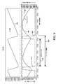
図9は、上述したもの(L12・430およびC12・438;L22・431およびC22・440)のように、再構成フィルタによってパルス振幅変調(PAM)電流パルスに変換された、パルス幅変調パルスの変換後の信号ダイアグラムを示している。短期間の略矩形状の電圧パルス902は、Q1・404のドレイン側451(図4)の電圧である。符号908が付されたパルス幅は、ライン411(図4)上の信号Q1Gのパルス幅に接近し、その周期910はPAMCC400のスイッチング周期である。この電圧は、トランス407およびPV401の電流を、トライアックCR11・424またはCR12・425を介して(上述したように、コントローラ412からの制御信号のそのときの状態に応じて)、再構成フィルタの1つの入力に向かわせる。曲線的な半波長整流正弦波904は、再構成フィルタの出力である。入力パルスのパルス幅908(近似的に)が増加すると、出力波形フォーム904の振幅が増加する。グラフの一番上の三角波フォーム906は、共通の時間ウィンドウ中にPV・401を通る電流の変化を示している。出力波形906は、再構成フィルタに与えられる相対的に大きなパルス幅変調電流パルスとは独立に相対的に一定なPV401の電流を維持する際の、トランス407の影響を示している。
FIG. 9 illustrates a pulse width modulated pulse converted to a pulse amplitude modulated (PAM) current pulse by a reconstruction filter, as described above (L12 · 430 and C12 · 438; L22 · 431 and C22 · 440). The signal diagram after conversion is shown. A
図10は、図11、図12および図13に示されることとなるグリッド正弦波サイクルの狭小なタイムスライスを示している。 FIG. 10 shows a narrow time slice of the grid sine wave cycle that would be shown in FIGS. 11, 12 and 13.
図11は、単一のPAMCC400のパルス振幅変調された出力電流を示している。なお、示された振幅が、サイクル例1101上に示すように、グリッド電圧の正のピークの近傍の小さい時間部分についてのものであることに留意されたい。個々のパルス1104は、スイッチング周波数の周期と等しい周期1106、例えば(1/30kHz)を有している。
FIG. 11 shows the pulse amplitude modulated output current of a
図12では、2つのPAMCC(各々がPAMCC400に従う)の2の個別の電流(1200.1および1200.2)は、スイッチング周波数の周期の2分の1離れて、位相が合わされている。上記出力波形1202は、2つのPAMCC出力電流1200.1および1200.2の和である。なお、合計電流1202は、単一のPAMCC(図11を参照)のリップルよりはるかに小さなリップルを有し、単一のインバータのリップル周波数の2倍のリップル周波数を有していることに留意されたい。合計電流1202は、ゼロに戻ることはない。 In FIG. 12, the two separate currents (1200.1 and 1200.2) of the two PAMCCs (each according to PAMCC 400) are phased apart by a half of the period of the switching frequency. The output waveform 1202 is the sum of two PAMCC output currents 1200.1 and 1200.2. Note that the total current 1202 has a much smaller ripple than that of a single PAMCC (see FIG. 11) and has a ripple frequency twice that of a single inverter. I want. The total current 1202 never returns to zero.
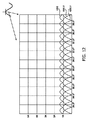
2つのPAMCC400出力の電流の合計に続いて、図13は、8のPAMCC(ライン1300は代表であり、各波形には番号が付されていない)の個々の出力電流を示し、その各々が、スイッチング周波数の周期を跨いで均等に位相がずれている。例えば、30kHzのスイッチング周波数を使用するシステムについては、周期は33.3マイクロ秒であり、各相は、前の出力電流波形に対して、(33.3/8)または4.167マイクロ秒だけ遅延される。任意の数のPAMCC400をそのように合計することができる。合計数が増加するとき、それらは、より小さい数(1/(スイッチング周波数)*n;ここで、“n”は合計されるPAMCCの数である)だけ各相が遅延される。なお、図13に示される合計電流は、個々のPAMCC(図12)のリップル電流のごく一部分だけを有しており、個々のPAMCCのリップル周波数の8倍のリップル周波数を有していることに留意されたい。各PAMCC400がグリッド正弦波上にポイントを生成している場合、PAMCCのセットの位相をずらして合計し、コンバータのアレイを生成する、一連のPAM電流パルスは、電流のグリッド正弦波を非常に高精度および非常に低ノイズ(リップル)で効率良く復調することとなる。任意の数のアレイコンバータを、このように位相をずらして合計することができる。PAMCCの数が増加するに連れて、リップル振幅が減少する一方、リップル周波数が増加する。一実施形態では、複数のPAMCC400の個々の出力電流の2またはそれ以上は、互いに同調している。幾つかの実施形態では、スイッチング周波数は、グリッド周波数、例えば、米国における60Hzとは無関係となるように選択され、リップルが高調波歪みを表さないようになる。PAMCC出力上で変調される信号は任意である。幾つかの実施形態では、多重信号がPAMCC出力上で変調され、そのような信号の1つが、例えば、任意の2またはそれ以上のPAMCCモジュール間の通信を提供することができる。PAMCC変調は、グリッド信号中の歪みを補正するために使用されることもある。
Following the sum of the currents of the two
配列されたPAMCC400の位相調整を選ぶ幾つかの方法のうちの1つは、各PAMCC400にタイミングスロット番号を予め割り当てるものであり、第1スロットがゼロ交差の後に予定され、各PAMCC400が、予め設定された(すなわち、割り当てられた)順序でそのPAM信号を発するものとされる。
One of several ways of choosing the phase adjustment of the arrayed
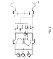
図14に例示される代替的な実施形態では、別のトランジスタが加えられ、Q1A・1402およびQ1B・1404が、図4の回路で示して説明した単一のトランジスタQ1・404に取って代わる。2つのトランジスタQ1A・1402およびQ1B・1404を使用することには幾つかの潜在的な利点が有り、それには、各トランジスタを跨ぐ電圧を低減すること、Q1・404のRds_on条件と比較して各トランジスタのRds_on(“オン”抵抗)条件をより緩和することを可能にすること、相対的に低電圧および安定したPV401のアノードおよびカソード端部に対して各トランジスタを駆動することを可能にすることが含まれる。この構成では、Q1A・1402およびQ1B・1404はともに、前述したQ1・404のように同時にオンおよびオフ状態とされる。回路動作のその他の面はすべて同じままである。Q1A・1402およびQ1B・1404は、異なるトランジスタ型式であり、よって、それらの制御ゲートへの個々の信号は、コントローラ1412によって与えられる。コントローラ1412は、その他の点では、図12のコントローラ412と同じであり、追加の出力端子が、ライン1401および1403を介して制御ゲートQ1A・1402およびQ1B・1404に接続されている。
In the alternative embodiment illustrated in FIG. 14, another transistor is added, and
幾つかの実施形態では、安全性、メンテナンスまたはその他の目的のためにシステムをシャットダウンすることができる。シャットダウン方法の一例が図15に示されている。図示のように、トランジスタTR1・1502および中継器S1・1504が加えられている。なお、この例は、2つのトランジスタQ1A・1402およびQ1B・1404を含むが、同じシャットダウン対策を図4の回路に加えることができ、その場合には、2つのトランジスタQ1AおよびQ1Bが単一のトランジスタQ1・404により置き換えられることに留意されたい。トランジスタTR1・1502および中継器S1・1504は、照明されて電力を生成するPV401に接続されている間に、PAMCCの安全なシャットダウンを提供する。シャットダウンプロセスは、ライン1506上のコントローラ1512からの信号TR1Bを与えることによって開始され、ライン1506は、トランジスタ1502の制御ゲートに接続されている。トランジスタTR1・1502がオン状態とされるとき、TR1は、PV401によって生成される電流のための短いパスを形成し、それにより、PV401を跨ぐ電圧が小さなレベルに減少されることとなる。この時点で、Q1A・1402およびQ1C・1404は、コイルL1・406およびL2・405中の電流が低レベルに低下することを可能にするように電圧が加えられる。コイルL1およびL2が放電された後、中継器S1・1504が開放される。その際に、グリッドへのパスが開き、Q1A・1402およびQ1B・1404がオフ状態とされ、その後に、TR1・1502がオフ状態とされる。この構成では、それ以上の電力が生成されないものとなる。
In some embodiments, the system can be shut down for safety, maintenance or other purposes. An example of a shutdown method is shown in FIG. As shown in the figure, transistors TR1 and 1502 and repeaters S1 and 1504 are added. Although this example includes two transistors Q1A and 1402 and Q1B and 1404, the same shutdown countermeasure can be added to the circuit of FIG. 4, in which case the two transistors Q1A and Q1B are a single transistor. Note that it is replaced by Q1 · 404. Transistors TR1 1502 and
図16は本発明の実施のための別の代替的トポロジーを示している。直流電源1602は、ライン1610のバス上の電流を複数のPAMCC1604.1、1604.nユニットに与える。直流電源1602は、例えば、バッテリ、並列の多重バッテリ(並列のバッテリの幾つかは、直列のバッテリにより構成することができる)、AC線源からDC電流を与える電力供給装置など、様々な直流電源の何れかとすることができる。上述したように、PAMCC1604.1、1604.nの電流出力は、位相がずれてバス1612上で合計されて、負荷1606にAC電力を与える。負荷1606は外部グリッドであってもよい。
FIG. 16 shows another alternative topology for the implementation of the present invention. The
Claims (40)
2またはそれ以上の直流電源と、
各直流電源に接続されるパルス振幅変調電流コンバータ(“コンバータ”)とを備え、
前記コンバータの各々が、直流電流をそれぞれの直流電源から受け取るとともに、前記コンバータの出力端子でパルス振幅変調された電流パルスを与え、
各コンバータの前記出力端子が、前記システム内のその他のコンバータすべての出力端子と並列に電気的に接続され、
少なくとも2のコンバータの前記電流パルスが、互いに位相がずれており、
前記コンバータの前記パルス出力で変調される信号が復調されるように、前記コンバータすべての前記電流パルスが合計されることを特徴とするシステム。 A system for converting power,
Two or more DC power supplies;
With a pulse amplitude modulated current converter ("converter") connected to each DC power source,
Each of the converters receives a direct current from a respective direct current power source and provides a pulse of amplitude modulated pulse at the output terminal of the converter,
The output terminal of each converter is electrically connected in parallel with the output terminals of all other converters in the system;
The current pulses of at least two converters are out of phase with each other;
The system wherein the current pulses of all of the converters are summed so that a signal modulated with the pulse output of the converter is demodulated.
各コンバータの前記電流パルスが、その他のコンバータすべての前記電流パルスに対して位相がずれていることを特徴とするシステム。 The system of claim 1, wherein
The system wherein the current pulses of each converter are out of phase with the current pulses of all other converters.
前記信号が、60サイクルの交流電圧であることを特徴とするシステム。 The system of claim 1, wherein
The system wherein the signal is a 60 cycle AC voltage.
前記信号が、直流電圧のほぼ固定された値であることを特徴とするシステム。 The system of claim 1, wherein
A system wherein the signal is a substantially fixed value of a DC voltage.
前記信号が方形波であることを特徴とするシステム。 The system of claim 1, wherein
A system wherein the signal is a square wave.
前記信号が三角波であることを特徴とするシステム。 The system of claim 1, wherein
The system wherein the signal is a triangular wave.
前記信号がガウス波であることを特徴とするシステム。 The system of claim 1, wherein
A system wherein the signal is a Gaussian wave.
前記信号が、データを伝えるための通信信号を与えることを特徴とするシステム。 The system of claim 1, wherein
The system wherein the signal provides a communication signal for carrying data.
前記通信信号が、所与のコンバータから前記システム内の少なくとも1のその他のコンバータにデータを与えることを特徴とするシステム。 The system of claim 8, wherein
The system wherein the communication signal provides data from a given converter to at least one other converter in the system.
前記通信信号が、所与のコンバータから前記システム内のその他のコンバータのすべてにデータを与えることを特徴とするシステム。 The system of claim 8, wherein
The system wherein the communication signal provides data from a given converter to all of the other converters in the system.
前記データが位相データを含むことを特徴とするシステム。 The system of claim 8, wherein
The system wherein the data includes phase data.
前記データが制御コマンドを含むことを特徴とするシステム。 The system of claim 8, wherein
The system wherein the data includes a control command.
前記データが動作データを含むことを特徴とするシステム。 The system of claim 8, wherein
The system wherein the data includes operational data.
前記2またはそれ以上の直流電源が光起電性パネルであることを特徴とするシステム。 The system of claim 1, wherein
The system characterized in that the two or more direct current power sources are photovoltaic panels.
前記2またはそれ以上の直流電源が風力発電機であることを特徴とするシステム。 The system of claim 1, wherein
The system characterized in that the two or more DC power sources are wind power generators.
前記2またはそれ以上の直流電源が潮力発電機であることを特徴とするシステム。 The system of claim 1, wherein
The system characterized in that the two or more DC power sources are tidal power generators.
前記2またはそれ以上の直流電源が圧電式発電機であることを特徴とするシステム。 The system of claim 1, wherein
The system characterized in that the two or more DC power sources are piezoelectric generators.
前記2またはそれ以上の直流電源がバッテリであることを特徴とするシステム。 The system of claim 1, wherein
The system characterized in that the two or more DC power sources are batteries.
前記通信信号が前記信号に重畳されることを特徴とするシステム。 The system of claim 8, wherein
The system, wherein the communication signal is superimposed on the signal.
前記電流パルスが、前記信号の任意の歪みを低減するように修正されることを特徴とするシステム。 The system of claim 1, wherein
The system wherein the current pulse is modified to reduce any distortion of the signal.
直流電源と、
前記直流電源に接続される複数のパルス振幅変調電流コンバータ(“コンバータ”)とを備え、
前記コンバータの各々が、前記直流電源から直流電流を受け取るとともに、前記コンバータの出力端子でパルス振幅変調された電流パルスを与え、
各コンバータの前記出力端子が、前記システム内のその他のコンバータすべての出力端子と並列に電気的に接続され、
少なくとも2のコンバータの前記電流パルスが、互いに位相がずれており、
前記コンバータの前記パルス出力で変調される信号が復調されるように、前記コンバータすべての前記電流パルスが合計されることを特徴とするシステム。 A system for converting power,
DC power supply,
A plurality of pulse amplitude modulation current converters ("converters") connected to the DC power source;
Each of the converters receives a direct current from the direct current power source and provides a pulse of current that is pulse amplitude modulated at the output terminal of the converter,
The output terminal of each converter is electrically connected in parallel with the output terminals of all other converters in the system;
The current pulses of at least two converters are out of phase with each other;
The system wherein the current pulses of all of the converters are summed so that a signal modulated with the pulse output of the converter is demodulated.
各コンバータの前記電流パルスが、その他のコンバータすべての前記電流パルスに対して位相がずれていることを特徴とするシステム。 The system of claim 21, wherein
The system wherein the current pulses of each converter are out of phase with the current pulses of all other converters.
前記信号が、60サイクルの交流電圧であることを特徴とするシステム。 The system of claim 21, wherein
The system wherein the signal is a 60 cycle AC voltage.
前記信号が、直流電圧のほぼ固定された値であることを特徴とするシステム。 The system of claim 21, wherein
A system wherein the signal is a substantially fixed value of a DC voltage.
前記信号が方形波であることを特徴とするシステム。 The system of claim 21, wherein
A system wherein the signal is a square wave.
前記信号が三角波であることを特徴とするシステム。 The system of claim 21, wherein
The system wherein the signal is a triangular wave.
前記信号がガウス波であることを特徴とするシステム。 The system of claim 21, wherein
A system wherein the signal is a Gaussian wave.
前記信号が、データを伝えるための通信信号を与えることを特徴とするシステム。 The system of claim 21, wherein
The system wherein the signal provides a communication signal for carrying data.
前記通信信号が、所与のコンバータから前記システム内の少なくとも1のその他のコンバータにデータを与えることを特徴とするシステム。 The system of claim 28, wherein
The system wherein the communication signal provides data from a given converter to at least one other converter in the system.
前記通信信号が、所与のコンバータから前記システム内のその他のコンバータのすべてにデータを与えることを特徴とするシステム。 The system of claim 28, wherein
The system wherein the communication signal provides data from a given converter to all of the other converters in the system.
前記データが位相データを含むことを特徴とするシステム。 The system of claim 28, wherein
The system wherein the data includes phase data.
前記データが制御コマンドを含むことを特徴とするシステム。 The system of claim 28, wherein
The system wherein the data includes a control command.
前記データが動作データを含むことを特徴とするシステム。 The system of claim 28, wherein
The system wherein the data includes operational data.
前記直流電源が光起電性パネルであることを特徴とするシステム。 The system of claim 21, wherein
A system wherein the DC power source is a photovoltaic panel.
前記直流電源が風力発電機であることを特徴とするシステム。 The system of claim 21, wherein
The DC power supply is a wind power generator.
前記直流電源が潮力発電機であることを特徴とするシステム。 The system of claim 21, wherein
The system, wherein the DC power source is a tidal power generator.
前記直流電源が圧電式発電機であることを特徴とするシステム。 The system of claim 21, wherein
The DC power supply is a piezoelectric generator.
前記直流電源がバッテリであることを特徴とするシステム。 The system of claim 21, wherein
The DC power supply is a battery.
前記通信信号が前記信号に重畳されることを特徴とするシステム。 The system of claim 28, wherein
The system, wherein the communication signal is superimposed on the signal.
前記電流パルスが、前記信号の任意の歪みを低減するように修正されることを特徴とするシステム。 The system of claim 21, wherein
The system wherein the current pulse is modified to reduce any distortion of the signal.
Applications Claiming Priority (5)
| Application Number | Priority Date | Filing Date | Title |
|---|---|---|---|
| US12/061,025 US7719864B2 (en) | 2008-04-02 | 2008-04-02 | Pulse amplitude modulated current converter |
| US12/061,025 | 2008-04-02 | ||
| US12/276,411 US7929324B1 (en) | 2008-04-02 | 2008-11-23 | Blade architecture array converter |
| US12/276,411 | 2008-11-23 | ||
| PCT/US2009/039368 WO2009124221A2 (en) | 2008-04-02 | 2009-04-02 | Blade architecture array converter |
Publications (2)
| Publication Number | Publication Date |
|---|---|
| JP2011517269A true JP2011517269A (en) | 2011-05-26 |
| JP2011517269A5 JP2011517269A5 (en) | 2012-05-24 |
Family
ID=41136115
Family Applications (1)
| Application Number | Title | Priority Date | Filing Date |
|---|---|---|---|
| JP2011503188A Pending JP2011517269A (en) | 2008-04-02 | 2009-04-02 | Blade structure array converter |
Country Status (9)
| Country | Link |
|---|---|
| US (1) | US7929324B1 (en) |
| EP (1) | EP2272164A2 (en) |
| JP (1) | JP2011517269A (en) |
| KR (1) | KR20110005834A (en) |
| CN (1) | CN102047557A (en) |
| BR (1) | BRPI0906546A2 (en) |
| MX (1) | MX2010010868A (en) |
| TW (1) | TW200950300A (en) |
| WO (1) | WO2009124221A2 (en) |
Families Citing this family (8)
| Publication number | Priority date | Publication date | Assignee | Title |
|---|---|---|---|---|
| US20100301676A1 (en) * | 2009-05-28 | 2010-12-02 | General Electric Company | Solar power generation system including weatherable units including photovoltaic modules and isolated power converters |
| EP2564502A4 (en) * | 2010-04-26 | 2018-01-24 | Queen's University At Kingston | Power converter for a power generator |
| JP5928736B2 (en) * | 2010-08-31 | 2016-06-01 | エスエムエー ソーラー テクノロジー アーゲー | Inverter with AC interface for AC module connection |
| US8774974B2 (en) * | 2011-07-15 | 2014-07-08 | First Solar, Inc. | Real-time photovoltaic power plant control system |
| US9234506B2 (en) * | 2011-10-14 | 2016-01-12 | Vestas Wind Systems A/S | Estimation of wind properties using a light detection and ranging device |
| WO2013112981A1 (en) * | 2012-01-26 | 2013-08-01 | Cameron D Kevin | Circuit for transferring power between a direct current line and an alternating-current line |
| US20150108851A1 (en) * | 2013-10-19 | 2015-04-23 | UltraSolar Technology, Inc. | Photovoltaic systems with shaped high frequency electric pulses |
| US9496710B2 (en) * | 2014-12-29 | 2016-11-15 | Solarcity Corporation | Rapid shutdown solid state circuit for photovoltaic energy generation systems |
Citations (4)
| Publication number | Priority date | Publication date | Assignee | Title |
|---|---|---|---|---|
| US4719550A (en) * | 1986-09-11 | 1988-01-12 | Liebert Corporation | Uninterruptible power supply with energy conversion and enhancement |
| US5642275A (en) * | 1995-09-14 | 1997-06-24 | Lockheed Martin Energy System, Inc. | Multilevel cascade voltage source inverter with seperate DC sources |
| US20040225225A1 (en) * | 2001-01-09 | 2004-11-11 | Naumov Valery Arkadievich | Method and device for registering and processing plethysmograms |
| US20070139137A1 (en) * | 2005-12-20 | 2007-06-21 | Honeywell International Inc. | Apparatus and method for measuring the position of a member |
Family Cites Families (13)
| Publication number | Priority date | Publication date | Assignee | Title |
|---|---|---|---|---|
| US5677833A (en) * | 1995-05-16 | 1997-10-14 | Raytheon Company | Power conditioning system for a four quadrant photovoltaic array with an inverter for each array quadrant |
| JP3697121B2 (en) * | 1998-10-15 | 2005-09-21 | キヤノン株式会社 | Photovoltaic power generation apparatus and control method thereof |
| US6603619B1 (en) * | 1999-01-07 | 2003-08-05 | Sharp Kabushiki Kaisha | Magnetic storage medium and heat assisted recording and reproduction method |
| US6198314B1 (en) * | 1999-01-25 | 2001-03-06 | Motorola Inc. | Sample and hold circuit and method therefor |
| FR2855677B1 (en) * | 2003-05-30 | 2016-11-04 | Valeo Equip Electr Moteur | PULSE WIDTH MODULATION CONTROL CIRCUIT FOR MULTI MODE ELECTRIC MACHINE AND MULTI MODE ELECTRIC MACHINE EQUIPPED WITH SUCH A CONTROL CIRCUIT |
| US6969967B2 (en) * | 2003-12-12 | 2005-11-29 | Ut-Battelle Llc | Multi-level dc bus inverter for providing sinusoidal and PWM electrical machine voltages |
| US20050139259A1 (en) * | 2003-12-30 | 2005-06-30 | Robert Steigerwald | Transformerless power conversion in an inverter for a photovoltaic system |
| JP4884665B2 (en) * | 2004-11-12 | 2012-02-29 | ローム株式会社 | DC-AC converter, its controller IC, and DC-AC converter parallel operation system |
| DE102004060698B3 (en) * | 2004-12-16 | 2006-06-14 | Infineon Technologies Ag | Polar modulator for use in communication system, has filter provided downstream of output of pulse width modulator, for suppressing harmonic portions of fundamental value of signal measurable at output |
| CN1980033A (en) * | 2005-11-30 | 2007-06-13 | 硕颉科技股份有限公司 | DC./ac. convertion driving circuit |
| US7893346B2 (en) * | 2006-09-28 | 2011-02-22 | Jack Nachamkin | Integrated voltaic energy system |
| US7719864B2 (en) * | 2008-04-02 | 2010-05-18 | Array Converter, Inc. | Pulse amplitude modulated current converter |
| US7884500B2 (en) * | 2008-04-22 | 2011-02-08 | Array Converter Inc. | High voltage array converter |
-
2008
- 2008-11-23 US US12/276,411 patent/US7929324B1/en not_active Expired - Fee Related
-
2009
- 2009-04-02 JP JP2011503188A patent/JP2011517269A/en active Pending
- 2009-04-02 TW TW98111049A patent/TW200950300A/en unknown
- 2009-04-02 BR BRPI0906546-6A patent/BRPI0906546A2/en not_active IP Right Cessation
- 2009-04-02 EP EP20090726777 patent/EP2272164A2/en not_active Withdrawn
- 2009-04-02 KR KR1020107024596A patent/KR20110005834A/en not_active Application Discontinuation
- 2009-04-02 MX MX2010010868A patent/MX2010010868A/en unknown
- 2009-04-02 WO PCT/US2009/039368 patent/WO2009124221A2/en active Application Filing
- 2009-04-02 CN CN2009801203053A patent/CN102047557A/en active Pending
Patent Citations (4)
| Publication number | Priority date | Publication date | Assignee | Title |
|---|---|---|---|---|
| US4719550A (en) * | 1986-09-11 | 1988-01-12 | Liebert Corporation | Uninterruptible power supply with energy conversion and enhancement |
| US5642275A (en) * | 1995-09-14 | 1997-06-24 | Lockheed Martin Energy System, Inc. | Multilevel cascade voltage source inverter with seperate DC sources |
| US20040225225A1 (en) * | 2001-01-09 | 2004-11-11 | Naumov Valery Arkadievich | Method and device for registering and processing plethysmograms |
| US20070139137A1 (en) * | 2005-12-20 | 2007-06-21 | Honeywell International Inc. | Apparatus and method for measuring the position of a member |
Also Published As
| Publication number | Publication date |
|---|---|
| BRPI0906546A2 (en) | 2015-07-07 |
| KR20110005834A (en) | 2011-01-19 |
| US7929324B1 (en) | 2011-04-19 |
| WO2009124221A3 (en) | 2010-01-14 |
| CN102047557A (en) | 2011-05-04 |
| TW200950300A (en) | 2009-12-01 |
| EP2272164A2 (en) | 2011-01-12 |
| WO2009124221A2 (en) | 2009-10-08 |
| MX2010010868A (en) | 2010-12-17 |
Similar Documents
| Publication | Publication Date | Title |
|---|---|---|
| US8093754B2 (en) | High voltage array converter | |
| US7719864B2 (en) | Pulse amplitude modulated current converter | |
| Islam et al. | Single phase transformerless inverter topologies for grid-tied photovoltaic system: A review | |
| JP2011517269A (en) | Blade structure array converter | |
| CN107005151B (en) | Starting of HVDC converters | |
| US9431922B2 (en) | ARC fault protection for power conversion | |
| CN104081647B (en) | Stack voltage source inventer with independent DC power supply | |
| EP2897287B1 (en) | Photovoltaic module | |
| US20070273338A1 (en) | Transformerless Utility-Grid-Interactive Inverter | |
| US20100149847A1 (en) | Apparatus providing bias to solar cells | |
| KR101772541B1 (en) | Power supply device, and power supply system including the same | |
| US20120187768A1 (en) | Low filter capacitance power systems, structures, and processes for solar plants | |
| JP6124909B2 (en) | Single-phase inverter controlled cooperatively to supply single-phase, two-phase or three-phase unipolar electricity | |
| Paulino et al. | A review of the main inverter topologies applied on the integration of renewable energy resources to the grid | |
| CN104578171B (en) | A kind of control method of direct current photovoltaic generating module | |
| Pathy et al. | A modified module integrated—Interleaved boost converter for standalone photovoltaic (PV) application | |
| US9548610B2 (en) | Control method for arranging DC/AC converters in parallel | |
| Badhoutiya et al. | Boost control for PV applications using impedance source inverter | |
| KR20150085413A (en) | Photovoltaic module | |
| EP2897267B1 (en) | Power conversion apparatus and photovoltaic module including the same | |
| CN104467007A (en) | Control system for single phase cascading multi-level photovoltaic grid-connected inverter | |
| WO2013098844A2 (en) | Grid tie inverter |
Legal Events
| Date | Code | Title | Description |
|---|---|---|---|
| A521 | Request for written amendment filed |
Free format text: JAPANESE INTERMEDIATE CODE: A523 Effective date: 20120323 |
|
| A621 | Written request for application examination |
Free format text: JAPANESE INTERMEDIATE CODE: A621 Effective date: 20120323 |
|
| A521 | Request for written amendment filed |
Free format text: JAPANESE INTERMEDIATE CODE: A523 Effective date: 20130321 |
|
| A131 | Notification of reasons for refusal |
Free format text: JAPANESE INTERMEDIATE CODE: A131 Effective date: 20130730 |
|
| A601 | Written request for extension of time |
Free format text: JAPANESE INTERMEDIATE CODE: A601 Effective date: 20131004 |
|
| A602 | Written permission of extension of time |
Free format text: JAPANESE INTERMEDIATE CODE: A602 Effective date: 20131011 |
|
| A02 | Decision of refusal |
Free format text: JAPANESE INTERMEDIATE CODE: A02 Effective date: 20140311 |