KR100639007B1 - Light emitting display and driving method thereof - Google Patents
Light emitting display and driving method thereof Download PDFInfo
- Publication number
- KR100639007B1 KR100639007B1 KR1020050044696A KR20050044696A KR100639007B1 KR 100639007 B1 KR100639007 B1 KR 100639007B1 KR 1020050044696 A KR1020050044696 A KR 1020050044696A KR 20050044696 A KR20050044696 A KR 20050044696A KR 100639007 B1 KR100639007 B1 KR 100639007B1
- Authority
- KR
- South Korea
- Prior art keywords
- transistor
- emission control
- light emitting
- pixel
- scan
- Prior art date
Links
Images


Classifications
-
- G—PHYSICS
- G09—EDUCATION; CRYPTOGRAPHY; DISPLAY; ADVERTISING; SEALS
- G09G—ARRANGEMENTS OR CIRCUITS FOR CONTROL OF INDICATING DEVICES USING STATIC MEANS TO PRESENT VARIABLE INFORMATION
- G09G3/00—Control arrangements or circuits, of interest only in connection with visual indicators other than cathode-ray tubes
- G09G3/20—Control arrangements or circuits, of interest only in connection with visual indicators other than cathode-ray tubes for presentation of an assembly of a number of characters, e.g. a page, by composing the assembly by combination of individual elements arranged in a matrix no fixed position being assigned to or needed to be assigned to the individual characters or partial characters
- G09G3/22—Control arrangements or circuits, of interest only in connection with visual indicators other than cathode-ray tubes for presentation of an assembly of a number of characters, e.g. a page, by composing the assembly by combination of individual elements arranged in a matrix no fixed position being assigned to or needed to be assigned to the individual characters or partial characters using controlled light sources
- G09G3/30—Control arrangements or circuits, of interest only in connection with visual indicators other than cathode-ray tubes for presentation of an assembly of a number of characters, e.g. a page, by composing the assembly by combination of individual elements arranged in a matrix no fixed position being assigned to or needed to be assigned to the individual characters or partial characters using controlled light sources using electroluminescent panels
- G09G3/32—Control arrangements or circuits, of interest only in connection with visual indicators other than cathode-ray tubes for presentation of an assembly of a number of characters, e.g. a page, by composing the assembly by combination of individual elements arranged in a matrix no fixed position being assigned to or needed to be assigned to the individual characters or partial characters using controlled light sources using electroluminescent panels semiconductive, e.g. using light-emitting diodes [LED]
- G09G3/3208—Control arrangements or circuits, of interest only in connection with visual indicators other than cathode-ray tubes for presentation of an assembly of a number of characters, e.g. a page, by composing the assembly by combination of individual elements arranged in a matrix no fixed position being assigned to or needed to be assigned to the individual characters or partial characters using controlled light sources using electroluminescent panels semiconductive, e.g. using light-emitting diodes [LED] organic, e.g. using organic light-emitting diodes [OLED]
- G09G3/3225—Control arrangements or circuits, of interest only in connection with visual indicators other than cathode-ray tubes for presentation of an assembly of a number of characters, e.g. a page, by composing the assembly by combination of individual elements arranged in a matrix no fixed position being assigned to or needed to be assigned to the individual characters or partial characters using controlled light sources using electroluminescent panels semiconductive, e.g. using light-emitting diodes [LED] organic, e.g. using organic light-emitting diodes [OLED] using an active matrix
- G09G3/3233—Control arrangements or circuits, of interest only in connection with visual indicators other than cathode-ray tubes for presentation of an assembly of a number of characters, e.g. a page, by composing the assembly by combination of individual elements arranged in a matrix no fixed position being assigned to or needed to be assigned to the individual characters or partial characters using controlled light sources using electroluminescent panels semiconductive, e.g. using light-emitting diodes [LED] organic, e.g. using organic light-emitting diodes [OLED] using an active matrix with pixel circuitry controlling the current through the light-emitting element
- G09G3/3241—Control arrangements or circuits, of interest only in connection with visual indicators other than cathode-ray tubes for presentation of an assembly of a number of characters, e.g. a page, by composing the assembly by combination of individual elements arranged in a matrix no fixed position being assigned to or needed to be assigned to the individual characters or partial characters using controlled light sources using electroluminescent panels semiconductive, e.g. using light-emitting diodes [LED] organic, e.g. using organic light-emitting diodes [OLED] using an active matrix with pixel circuitry controlling the current through the light-emitting element the current through the light-emitting element being set using a data current provided by the data driver, e.g. by using a two-transistor current mirror
- G09G3/325—Control arrangements or circuits, of interest only in connection with visual indicators other than cathode-ray tubes for presentation of an assembly of a number of characters, e.g. a page, by composing the assembly by combination of individual elements arranged in a matrix no fixed position being assigned to or needed to be assigned to the individual characters or partial characters using controlled light sources using electroluminescent panels semiconductive, e.g. using light-emitting diodes [LED] organic, e.g. using organic light-emitting diodes [OLED] using an active matrix with pixel circuitry controlling the current through the light-emitting element the current through the light-emitting element being set using a data current provided by the data driver, e.g. by using a two-transistor current mirror the data current flowing through the driving transistor during a setting phase, e.g. by using a switch for connecting the driving transistor to the data driver
-
- G—PHYSICS
- G09—EDUCATION; CRYPTOGRAPHY; DISPLAY; ADVERTISING; SEALS
- G09G—ARRANGEMENTS OR CIRCUITS FOR CONTROL OF INDICATING DEVICES USING STATIC MEANS TO PRESENT VARIABLE INFORMATION
- G09G3/00—Control arrangements or circuits, of interest only in connection with visual indicators other than cathode-ray tubes
- G09G3/20—Control arrangements or circuits, of interest only in connection with visual indicators other than cathode-ray tubes for presentation of an assembly of a number of characters, e.g. a page, by composing the assembly by combination of individual elements arranged in a matrix no fixed position being assigned to or needed to be assigned to the individual characters or partial characters
-
- G—PHYSICS
- G09—EDUCATION; CRYPTOGRAPHY; DISPLAY; ADVERTISING; SEALS
- G09G—ARRANGEMENTS OR CIRCUITS FOR CONTROL OF INDICATING DEVICES USING STATIC MEANS TO PRESENT VARIABLE INFORMATION
- G09G2300/00—Aspects of the constitution of display devices
- G09G2300/08—Active matrix structure, i.e. with use of active elements, inclusive of non-linear two terminal elements, in the pixels together with light emitting or modulating elements
- G09G2300/0809—Several active elements per pixel in active matrix panels
- G09G2300/0842—Several active elements per pixel in active matrix panels forming a memory circuit, e.g. a dynamic memory with one capacitor
- G09G2300/0852—Several active elements per pixel in active matrix panels forming a memory circuit, e.g. a dynamic memory with one capacitor being a dynamic memory with more than one capacitor
-
- G—PHYSICS
- G09—EDUCATION; CRYPTOGRAPHY; DISPLAY; ADVERTISING; SEALS
- G09G—ARRANGEMENTS OR CIRCUITS FOR CONTROL OF INDICATING DEVICES USING STATIC MEANS TO PRESENT VARIABLE INFORMATION
- G09G2300/00—Aspects of the constitution of display devices
- G09G2300/08—Active matrix structure, i.e. with use of active elements, inclusive of non-linear two terminal elements, in the pixels together with light emitting or modulating elements
- G09G2300/0809—Several active elements per pixel in active matrix panels
- G09G2300/0842—Several active elements per pixel in active matrix panels forming a memory circuit, e.g. a dynamic memory with one capacitor
- G09G2300/0861—Several active elements per pixel in active matrix panels forming a memory circuit, e.g. a dynamic memory with one capacitor with additional control of the display period without amending the charge stored in a pixel memory, e.g. by means of additional select electrodes
-
- G—PHYSICS
- G09—EDUCATION; CRYPTOGRAPHY; DISPLAY; ADVERTISING; SEALS
- G09G—ARRANGEMENTS OR CIRCUITS FOR CONTROL OF INDICATING DEVICES USING STATIC MEANS TO PRESENT VARIABLE INFORMATION
- G09G2310/00—Command of the display device
- G09G2310/02—Addressing, scanning or driving the display screen or processing steps related thereto
- G09G2310/0243—Details of the generation of driving signals
- G09G2310/0251—Precharge or discharge of pixel before applying new pixel voltage
-
- G—PHYSICS
- G09—EDUCATION; CRYPTOGRAPHY; DISPLAY; ADVERTISING; SEALS
- G09G—ARRANGEMENTS OR CIRCUITS FOR CONTROL OF INDICATING DEVICES USING STATIC MEANS TO PRESENT VARIABLE INFORMATION
- G09G2320/00—Control of display operating conditions
- G09G2320/02—Improving the quality of display appearance
- G09G2320/0247—Flicker reduction other than flicker reduction circuits used for single beam cathode-ray tubes
Landscapes
- Engineering & Computer Science (AREA)
- Physics & Mathematics (AREA)
- Computer Hardware Design (AREA)
- General Physics & Mathematics (AREA)
- Theoretical Computer Science (AREA)
- Control Of El Displays (AREA)
- Electroluminescent Light Sources (AREA)
- Control Of Indicators Other Than Cathode Ray Tubes (AREA)
Abstract
Description
도 1은 종래기술에 의한 전류구동형 화소를 나타내는 회로도이다. 1 is a circuit diagram showing a current-driven pixel according to the prior art.
도 2는 본 발명에 따른 발광 표시장치의 제 1 실시예를 나타내는 구조도이다. 2 is a structural diagram illustrating a first embodiment of a light emitting display device according to the present invention.
도 3은 본 발명에 따른 주사구동부의 동작을 나타내는 파형도이다.3 is a waveform diagram showing the operation of the scan driver according to the present invention.
도 4는 도 2의 발광표시장치에서 채용된 화소를 나타내는 회로도이다. 4 is a circuit diagram illustrating a pixel employed in the light emitting display device of FIG. 2.
도 5는 도 2의 발광표시장치에서 채용된 다른 화소를 나타내는 회로도이다. FIG. 5 is a circuit diagram illustrating another pixel employed in the light emitting display device of FIG. 2.
도 6은 본 발명에 따른 발광 표시장치의 제 2 실시예를 나타내는 구조도이다. 6 is a structural diagram illustrating a second embodiment of a light emitting display device according to the present invention.
도 7은 본 발명에 따른 주사구동부의 동작을 나타내는 파형도이다. 7 is a waveform diagram showing the operation of the scan driver according to the present invention.
도 8은 도 6의 발광 표시장치에서 채용된 화소를 나타내는 회로도이다. FIG. 8 is a circuit diagram illustrating a pixel employed in the light emitting display device of FIG. 6.
도 9는 도 6의 발광 표시장치에서 채용된 다른 화소를 나타내는 회로도이다. FIG. 9 is a circuit diagram illustrating another pixel employed in the light emitting display of FIG. 6.
도 10은 본 발명에 따른 발광 표시장치의 제 3 실시예의 구조를 나타내는 구조도이다. 10 is a structural diagram showing a structure of a third embodiment of a light emitting display device according to the present invention.
도 11은 발광표시장치에 깜빡임을 육안으로 관찰한 결과를 도시한 그래프를 나타낸다. 11 is a graph illustrating a result of visual observation of flickering in the light emitting display device.
***도면의 주요부분에 대한 부호설명****** Explanation of symbols on main parts of drawings ***
100: 화소부 110: 화소 100: pixel portion 110: pixel
200: 데이터 구동부 300: 주사 구동부200: data driver 300: scan driver
OLED: 발광소자OLED: light emitting element
본 발명은 발광 표시장치 및 발광표시장치 구동방법에 관한 것으로, 더욱 상세히 설명하면, 전류구동형화소회로를 포함하는 발광 표시장치에서 듀티비를 이용하여 발광소자에 전류를 공급함과 동시에 깜빡임 현상이 나타나지 않도록 하는 발광 표시장치 및 발광표시장치 구동방법에 관한 것이다. The present invention relates to a light emitting display device and a method of driving the light emitting display device. More specifically, the light emitting display device including the current-driven pixel circuit is used to supply current to the light emitting device by using a duty ratio and simultaneously flicker occurs. The present invention relates to a light emitting display device and a method of driving the light emitting display device.
최근, 음극선관(Cathode Ray Tube)의 단점인 무게와 부피를 줄일 수 있는 각종 평판 표시장치들이 개발되고 있다. 평판 표시장치로는 액정 표시장치(Liquid Crystal Display), 전계방출 표시장치(Field Emission Display), 플라즈마 표시패널(Plasma Display Panel) 및 유기 발광 소자(Organic Light emitting Device: 이하 발광소자 라 한다)를 이용한 유기 발광 표시장치 등이 있다. Recently, various flat panel displays have been developed to reduce weight and volume, which are disadvantages of cathode ray tubes. As a flat panel display device, a liquid crystal display device, a field emission display device, a plasma display panel, and an organic light emitting device are referred to as light emitting devices. Organic light emitting display devices;
평판표시장치 중 발광소자는 애노드 전극, 캐소드 전극 및 이들 사이에 위치하여 전자와 정공의 결합에 의하여 발광하는 발광층을 포함하고 발광층 내에서 전자와 정공의 재결합으로 인해 발광시키는 자발광소자로서, 액정 표시장치와 같이 별도의 광원을 필요로 하는 발광소자에 비하여 음극선관과 같은 빠른 응답속도를 가지는 장점을 갖고 있다. Among the flat panel display devices, the light emitting device includes an anode electrode, a cathode electrode, and a light emitting layer disposed therebetween to emit light by the combination of electrons and holes, and emits light by recombination of electrons and holes in the light emitting layer. Compared to a light emitting device that requires a separate light source, such as a device, it has the advantage of having a fast response speed, such as a cathode ray tube.
도 1은 종래기술에 의한 전류구동형 화소를 나타내는 회로도이다. 도 1을 참조하면, 화소는 발광소자(OLED) 및 화소회로를 포함하며, 화소회로는 제 1 트랜지스터(T1) 내지 제 4 트랜지스터(T4) 및 캐패시터(C1)를 포함한다. 그리고, 제 1 트랜지스터(T1) 내지 제 4 트랜지스터(T4)는 각각 게이트, 소스 및 드레인을 가지며 캐패시터(C1)는 제 1 전극과 제 2 전극을 가진다. 1 is a circuit diagram showing a current-driven pixel according to the prior art. Referring to FIG. 1, a pixel includes a light emitting device OLED and a pixel circuit, and the pixel circuit includes first to fourth transistors T1 to T4 and a capacitor C1. The first to fourth transistors T1 to T4 have a gate, a source, and a drain, respectively, and the capacitor C1 has a first electrode and a second electrode.
제 1 트랜지스터(T1)의 전류량은 제 2 트랜지스터(T2)를 통해 인가되는 데이터 전류에 의해 제어되도록 되어있다. 이때 인가된 데이터전류는 제 1 트랜지스터(T1)의 소스와 게이트 사이에 연결되어 있는 캐패시터(C1)에 의해서 일정기간 유지되게 된다. The current amount of the first transistor T1 is controlled by the data current applied through the second transistor T2. In this case, the applied data current is maintained for a certain period of time by the capacitor C1 connected between the source and the gate of the first transistor T1.
제 2 및 제 3 트랜지스터(T2, T3)의 게이트에는 주사선(Sn)이 연결되어 있고, 제 2 트랜지스터(T2)의 소스 측에는 데이터선(Dm)이 연결되어 있으며. 제 3 트랜지스터(T3)는 소스와 드레인이 제 1 트랜지스터(T1)의 드레인과 게이트에 연결된다. 또한, 제 4 트랜지스터(T4)는 소스는 제 1 전원(ELVdd)이 연결되고 드레인은 제 1 트랜지스터(T1)의 소스에 연결되며 게이트에는 발광제어선(En)이 연결된다. Scan lines Sn are connected to gates of the second and third transistors T2 and T3, and data lines Dm are connected to a source side of the second transistor T2. A source and a drain of the third transistor T3 are connected to the drain and the gate of the first transistor T1. In addition, the fourth transistor T4 has a source connected to a first power source ELVdd, a drain connected to a source of the first transistor T1, and a light emission control line En connected to a gate thereof.
이와 같은 구조의 화소의 동작을 살펴보면, 도 1에 도시된 바와 같이 제 2 및 제 3 트랜지스터(T2, T3)의 게이트에 인가되는 주사신호(sn)가 로우(low)가 되어 제 2 및 제 3 트랜지스터(T2, T3)가 온 되면, 제 1 트랜지스터(T1)는 다이오드 연결상태가 되고 데이터 전류(Idata) 값에 해당되는 전압이 캐패시터(C1)에 저장되 게 된다. Referring to the operation of the pixel having such a structure, as shown in FIG. 1, the scan signal sn applied to the gates of the second and third transistors T2 and T3 is turned low, thereby causing the second and third to be operated. When the transistors T2 and T3 are turned on, the first transistor T1 is diode connected and a voltage corresponding to the data current Idata is stored in the capacitor C1.
주사신호(sn)가 하이(high)가 되어 제 2 및 제 3 트랜지스터(T2, T3)가 오프(off)되고, 발광제어신호(En)가 로우(low)로 되어 제 4 트랜지스터(T4)가 온 되면, 전원이 공급되고 제 1 트랜지스터(T1)로부터 캐패시터(C1)에 저장된 전압값에 대응하는 전류가 발광소자(OLED)로 흘러 발광이 이루어진다. 이때 발광소자(OLED)에 흐르는 전류는 다음의 수학식 1과 같다.The scan signal sn becomes high, the second and third transistors T2 and T3 are turned off, and the emission control signal En is turned low, and the fourth transistor T4 is turned off. When turned on, power is supplied and a current corresponding to the voltage value stored in the capacitor C1 from the first transistor T1 flows to the light emitting element OLED to emit light. At this time, the current flowing through the light emitting device OLED is shown in

여기서, Idata는 데이터 전류, Vgs는 제 1 트랜지스터(T1)의 소스와 게이트 사이의 전압, Vth는 제 1 트랜지스터(T1)의 문턱전압, IOLED는 발광소자(OLED)에 흐르는 전류, β는 제 1 트랜지스터(T1)의 이득계수(gain factor)를 나타낸다. Where Idata is the data current, Vgs is the voltage between the source and gate of the first transistor T1, Vth is the threshold voltage of the first transistor T1, I OLED is the current flowing through the light emitting element OLED, and β is The gain factor of one transistor T1 is shown.
상기 수학식 1에서 나타낸 바와 같이 발광소자에 흐르는 전류(IOLED)는 제 1 트랜지스터(T1)의 문턱전압(Vth) 및 이동도(mobility)가 불균일하더라도 데이터 전류(Idata)와 동일하므로 데이터 구동부의 기입 전류원이 패널 전체를 통해 균일하다고 하면 균일한 디스플레이 특성을 얻을 수 있게 된다.As shown in
상기와 같은 전류기입 방식의 화소회로에서는 미세 전류를 컨트롤 해야 하기 때문에 데이터전류를 충전하는데 많은 시간이 필요하다는 문제점이 있다. 예를 들어, 데이터선 부하 커패시턴스가 30pF이라 가정할 경우 수십nA에서 수백 nA수준인 전류로 데이터선의 부하를 충전하려면 수msec의 시간이 필요하다.In the pixel circuit of the current write method as described above, since the microcurrent must be controlled, a long time is required to charge the data current. For example, assuming that the data line load capacitance is 30pF, a time of several msec is required to charge the load of the data line with a current of several tens of nA to several hundred nA.
이는 수십 ㎲수준인 라인시간(line time)을 고려 해볼 때 충전시간이 충분하지 못하며, 특히 낮은 휘도를 표현하는 경우 전류 값이 작아 충전시간이 더욱 많이 필요로 하는 문제점이 있다. This is not enough charging time in consideration of the line time (line time) of the tens of, level, especially in the case of expressing a low luminance, there is a problem that requires more charging time because the current value is small.
따라서, 본 발명은 상기 종래 기술의 문제점을 해결하기 위하여 창출된 것으로, 본 발명의 목적은 데이터전류를 크게 하여 데이터선에 데이터전류가 충전되는 속도를 줄일 수 있도록 하며 한 프레임 구간에서 발광소자가 발광하지 않는 구간을 분할하여 깜빡임 현상이 발생하지 않도록 하는 발광 표시장치 및 발광표시장치 구동방법을 제공하는 것이다. Therefore, the present invention was created to solve the problems of the prior art, and an object of the present invention is to increase the data current so as to reduce the rate at which the data current is charged in the data line and emit light in one frame period. The present invention provides a light emitting display device and a method of driving the light emitting display device in which a flickering phenomenon is prevented by dividing a section not to be generated.
상기 목적을 달성하기 위하여 본 발명의 제 1 측면은, 복수의 화소를 구비하여 화상을 표시하는 화소부, 상기 화소부에 주사신호와 발광제어신호를 전달하는 주사구동부 및 상기 화소부에 데이터전류를 전달하는 데이터구동부를 포함하며, 상기 화소는 상기 주사신호에 의해서 선택되어진 상기 데이터전류에 대응하여 발광을 수행하되, 상기 발광제어신호에 의해 한 프레임의 구간에 적어도 두번 발광하는 발광기간을 구비하여, 상기 데이터전류의 계조값보다 낮은 계조를 표현하는 발광표시장치를 제공하는 것이다. In order to achieve the above object, a first aspect of the present invention provides a pixel unit including a plurality of pixels for displaying an image, a scan driver for transmitting a scan signal and a light emission control signal to the pixel unit, and a data current to the pixel unit. And a data driver for transmitting the light, wherein the pixel emits light in response to the data current selected by the scan signal, and has a light emission period for emitting light at least twice in one frame by the light emission control signal. The present invention provides a light emitting display device that displays a gray scale lower than a gray scale value of the data current.
본 발명의 제 2 측면은, 복수의 화소를 구비하여 화상을 표시하는 화소부; 상기 화소부에 주사신호, 부스팅신호 발광제어신호를 전달하는 주사구동부; 및 상기 화소부에 데이터전류를 전달하는 데이터구동부를 포함하며, 상기 화소는 상기 주사신호에 의해서 선택되어진 상기 데이터전류에 대응하여 발광을 수행하되, 상기 발광제어신호에 의해 한 프레임의 구간에 적어도 두번 발광하는 발광기간을 구비하여, 상기 데이터전류의 계조값보다 낮은 계조를 표현하는 발광표시장치를 제공하는 것이다. According to a second aspect of the present invention, there is provided a display device including: a pixel unit including a plurality of pixels to display an image; A scan driver for transmitting a scan signal and a boosting signal emission control signal to the pixel unit; And a data driver for transmitting a data current to the pixel unit, wherein the pixel emits light in response to the data current selected by the scan signal, and at least twice in one frame section by the emission control signal. A light emitting display device having a light emitting period for emitting light and expressing a gray level lower than a gray value of the data current is provided.
본 발명의 제 3 측면은, 구동전류에 의해 발광하는 화소를 포함하는 발광표시장치 구동방법에 있어서, 데이터전류를 상기 화소에 전달하여 상기 데이터전류에 의해 상기 구동전류를 생성하는 단계 및 한프레임의 구간 동안 상기 구동전류를 적어도 두번 발광소자에 전달하여 상기 데이터전류의 계조값보다 낮은 계조로 표현하는 단계를 포함하는 발광표시장치 구동방법을 제공하는 것이다. According to a third aspect of the present invention, there is provided a method of driving a light emitting display device including a pixel that emits light by a driving current, the method comprising: generating a driving current by the data current by transferring a data current to the pixel; The present invention provides a method of driving a light emitting display device, the method comprising transmitting the driving current to the light emitting device at least twice during the interval and expressing the gray level lower than the gray value of the data current.
이하, 본 발명의 실시예를 첨부한 도면을 참조하여 설명하면 다음과 같다.Hereinafter, an embodiment of the present invention will be described with reference to the accompanying drawings.
도 2는 본 발명에 따른 발광 표시장치의 제 1 실시예를 나타내는 구조도이다. 도 2를 참조하여 설명하면, 발광 표시장치는 화상을 표현하는 화소부(100), 데이터전류를 전달하는 데이터구동부(200), 주사신호를 전달하는 주사구동부(300)를 포함한다. 2 is a structural diagram illustrating a first embodiment of a light emitting display device according to the present invention. Referring to FIG. 2, the light emitting display device includes a
화소부(100)는 발광소자와 화소회로로 이루어지는 복수의 화소(110), 행방향으로 배열된 복수의 주사선(S1,S2,...Sn-1,Sn), 열방향으로 배열된 복수의 데이터선(D1,D2,....Dm-1,Dm), 행방향으로 배열된 복수의 발광제어선(E1,E2,...En-1,En) 및 화소전원을 공급하는 복수의 제 1 전원선(Vdd)을 포함한다. The
그리고, 화소부(100)는 주사선(S1,S2,...Sn-1,Sn)에서 전달되는 주사신호에 의해 데이터전류가 데이터선(D1,D2,....Dm-1,Dm)을 통해 화소(110)에 전달되어 화소(110)에서 데이터전류에 대응되는 구동전류를 생성하며 발광제어선(E1,E2,...En-1,En)을 통해 전달되는 발광제어신호에 구동전류가 화소에 흐르도록 하여 화소(110)가 발광하도록 한다. The
데이터구동부(200)는 복수의 데이터선(D1,D2,....Dm-1,Dm)과 연결되어 복수의 데이터선(D1,D2,....Dm-1,Dm)을 통해 화소에 데이터 전류를 전달하여 데이터전류에 의해 화소(110)에서 구동전류를 생성하도록 한다. 또한, 데이터전류의 전류량을 구동전류의 전류량보다 크게 하여 큰 전류를 데이터선(D1,D2,....Dm-1,Dm)에 전달하여 데이터선(D1,D2,....Dm-1,Dm)이 빠르게 충전되도록 하여 데이터기입속도를 빠르게 구현할 수 있다. The
주사 구동부(300)는 화소부(100)의 측면에 구성되며, 복수의 주사선(S1,S2,...Sn-1,Sn)과 복수의 발광제어선(E1,E2,...En-1,En)에 연결되어 주사신호와 발광제어신호가 화소(110)에 전달하도록 한다. The
주사신호에 의해 데이터전류가 정해진 화소(110)에 전달되도록 하며 화소(110)발광제어신호에 의해 화소(110)에서 생성된 구동전류에 의해 정해진 시간동안 발광하도록 한다. 따라서, 화소(110)가 한 프레임의 구간동안 발광하는 구간과 발광하지 않는 구간으로 구분하여 한 프레임의 구간동안 발광표시장치의 휘도가 낮게 표현되도록 한다. The data current is transmitted to the
상기와 같이 한 프레임에서 화소(110)가 한번 발광하도록 한 경우에는 발광하지 않는 구간을 사용자가 인식하게 되어 깜빡임 현상이 나타나게 될 우려가 있다. As described above, when the
따라서, 발광제어신호에 의해 화소(110)가 한 프레임의 구간 동안 복수 번 발광을 하도록 하여 한 프레임이 구간 동안 화소(110)가 발광하지 않는 구간을 분할하여 발광하지 않는 구간이 한 프레임의 구간 내에서 짧게 여러 번 나타나도록 하여 사용자가 발광하지 않는 구간을 인식하지 못하도록 한다. Therefore, the light emitting control signal causes the
도 3은 본 발명에 따른 주사구동부의 동작을 나타내는 파형도이다. 도 3을 참조하여 설명하면, 주사구동부(300)는 주사신호를 발생하는 주사신호발생부와 발광제어신호를 발생하는 발광제어신호발생부로 구분된다. 제 1 스타트 펄스(1SP), 제 2 스타트 펄스(2SP) 및 클럭(CLK) 등을 입력받아 주사신호와 발광제어신호를 생성하여 화소부(100)에 전달한다. 3 is a waveform diagram showing the operation of the scan driver according to the present invention. Referring to FIG. 3, the
주사신호발생부는 시프트 레지스터로 구현되며 제 1 스타트 펄스(1SP)가 입력되어 제 1 스타트 펄스(1SP)를 시프트한 제 1 주사시프트신호(1SR)를 출력하고 제 1 주사시프트신호(1SR)를 이용하여 제 2 주사시프트신호(2SR)를 출력하며 제 2 주사시프트신호(2SR)를 이용하여 제 3 주사시프트신호(3SR)를 출력한다. 이러한 동작을 반복하여 n 개의 주사시프트신호를 출력하며 n 개의 주사시프트신호는 순차적으로 발생하게 된다. 그리고, 제 1 스타트 펄스((1SP))와 제 1 주사시프트신호(1SR)를 연산하여 첫번째 주사신호(s1)을 생성하고 제 1 주사시프트신호(1SR)와 제 2 주사시프트신호(2SR)를 연산하여 두번째 주사신호(s2)를 출력하며 제 2 주사시프트신호(2SR)와 제 3 주사시프트신호(3SR)를 연산하여 세번째 주사신호(s3)를 출력한다. 이러한 동작을 반복하여 n 개의 주사신호를 발생하며 각 주사시프트신호가 순차적으로 발생하기 때문에 n 개의 주사신호는 순차적으로 발생하게 된다. The scan signal generation unit is implemented as a shift register, and the first start pulse 1SP is input to output the first scan shift signal 1SR obtained by shifting the first start pulse 1SP and use the first scan shift signal 1SR. The second scan shift signal 2SR is output, and the third scan shift signal 3SR is output using the second scan shift signal 2SR. This operation is repeated to output n scan shift signals, and the n scan shift signals are sequentially generated. The first scan pulse s1 is generated by calculating the first start pulse 1SP and the first scan shift signal 1SR, and the first scan shift signal 1SR and the second scan shift signal 2SR are generated. The second scan signal s2 is output by the calculation, and the third scan signal s3 is output by calculating the second scan shift signal 2SR and the third scan shift signal 3SR. This operation is repeated to generate n scan signals, and since the scan shift signals are sequentially generated, the n scan signals are sequentially generated.
발광제어신호발생부 역시 시프트 레지스터로 구현되며 제 2 스타트 펄스(2SP)가 입력되어 제 2 스타트 펄스(2SP)를 시프트한 제 1 발광제어시프트신호(1ER)를 출력하고 제 1 발광제어시프트신호(1ER)를 이용하여 제 2 발광제어시프트신호(2ER)를 출력하며 제 2 발광제어시프트신호(2ER)를 이용하여 제 3 발광제어시프트신호(3ER)를 출력한다. 이러한 동작을 반복하여 n 개의 발광제어시프트신호를 출력하며 n 개의 발광제어시프트신호는 순차적으로 발생하게 된다. 그리고, 제 2 스타트 펄스(2SP)와 제 1 발광제어시프트신호(1ER)를 연산하여 첫번째 발광신호(e1)을 생성하고 제 1 발광제어시프트신호(1ER)와 제 2 발광제어시프트신호(2ER)를 연산하여 두번째 발광제어신호(e2)를 출력하며 제 2 발광제어시프트신호(2ER)와 제 3 발광제어시프트신호(3ER)를 연산하여 세번째 발광제어신호(e3)를 출력한다. 이러한 동작을 반복하여 n 개의 발광신호를 발생하며 각 발광제어시프트신호가 순차적으로 발생하기 때문에 n 개의 발광제어신호는 순차적으로 발생하게 된다. The light emission control signal generation unit is also implemented as a shift register, and the second start pulse 2SP is input to output the first light emission control shift signal 1ER obtained by shifting the second start pulse 2SP and the first light emission control shift signal ( The second emission control shift signal 2ER is output using 1ER and the third emission control shift signal 3ER is output using the second emission control shift signal 2ER. This operation is repeated to output n light emission control shift signals, and the n light emission control shift signals are sequentially generated. The first light emission signal e1 is generated by calculating the second start pulse 2SP and the first light emission control shift signal 1ER and the first light emission control shift signal 1ER and the second light emission control shift signal 2ER. The second light emission control signal e2 is output by calculating a and the second light emission control shift signal 2ER and the third light emission control shift signal 3ER are output to output the third light emission control signal e3. This operation is repeated to generate n light emission signals, and since the light emission control shift signals are sequentially generated, the n light emission control signals are sequentially generated.
그리고, 제 2 스타트 펄스(2SP)는 각각 두 개의 펄스로 구현하여 제 1 발광제어시프트신호(1ER)가 두 개의 펄스로 구현되도록 하며, 시프트레지스터의 동작에 따라 각 발광제어시프트신호는 두 개의 펄스로 구현되도록 한다. 특히, 제 2 스타트펄스(2SP)를 더 많은 수의 펄스로 구현하는 것도 가능하며, 이에 따라 발광제어 신호는 두 개 이상의 펄스를 포함하도록 한다. Each of the second start pulses 2SP is implemented by two pulses so that the first emission control shift signal 1ER is implemented by two pulses, and each emission control shift signal has two pulses according to the operation of the shift register. To be implemented. In particular, it is also possible to implement the second start pulse 2SP with a larger number of pulses, so that the emission control signal includes two or more pulses.
이때, 발광제어신호에서 펄스가 발생한 구간에서는 구동전류가 화소(110)에 전달되어 발광하고 펄스가 발생하지 않은 구간에서는 구동전류가 화소(110)에 전달되지 않아 발광하지 않게 된다. 따라서, 한 프레임의 구간에서 화소(110)가 발광하는 구간과 화소(110)가 발광하지 않는 구간이 교대로 나타나게 되어 화소(110)가 발광하지 않는 구간이 짧게 나타나게 되어 사용자가 화소(110)가 발광하지 않는 구간을 인식하지 못하게 되어 깜빡임 현상이 나타나지 않게 된다. In this case, the driving current is transmitted to the
도 4는 도 2의 발광표시장치에서 채용된 화소를 나타내는 회로도이다. 도 4를 참조하여 설명하면, 화소는 발광소자(OLED)와 화소회로를 포함하며, 화소회로는 제 1 내지 제 4 트랜지스터(M1 내지 M4)와 캐패시터(C1)를 포함한다. 그리고 제 1 내지 제 4 트랜지스터(M1 내지 M4)는 소스, 드레인 및 게이트를 구비하고 캐패시터(C1)는 제 1 전극과 제 2 전극을 구비한다. 4 is a circuit diagram illustrating a pixel employed in the light emitting display device of FIG. 2. Referring to FIG. 4, a pixel includes a light emitting device OLED and a pixel circuit, and the pixel circuit includes first to fourth transistors M1 to M4 and a capacitor C1. The first to fourth transistors M1 to M4 include a source, a drain, and a gate, and the capacitor C1 includes a first electrode and a second electrode.
제 1 내지 제 4 트랜지스터(M1 내지 M4)는 P 모스(MOS) 트랜지스터로 구현되며, 각 트랜지스터의 소스와 드레인은 물리적으로 차이가 없어 제 1 전극 및 제 2 전극으로 칭할 수 있다. The first to fourth transistors M1 to M4 are implemented as P MOS transistors, and the source and drain of each transistor may be referred to as a first electrode and a second electrode because they do not have physical differences.
제 1 트랜지스터(M1)는 소스는 화소전원에 연결되고 드레인은 제 1 노드(A)에 연결되며 게이트는 제 2 노드(B)에 연결되어 제 2 노드(B)의 전압에 따라 소스에서 드레인 방향으로 구동전류가 흐르도록 한다. The first transistor M1 has a source connected to the pixel power supply, a drain connected to the first node A, and a gate connected to the second node B, so that the source-to-drain direction depends on the voltage of the second node B. Drive current flows.
제 2 트랜지스터(M2)는 소스는 데이터선(Dm)에 연결되고 드레인은 제 2 노드 (B)에 연결되며 게이트는 주사선(Sn)에 연결되어 주사선(Sn)을 통해 전달되는 주사신호에 의해 제 2 노드(B)에 데이터전류를 전달한다. The second transistor M2 has a source connected to the data line Dm, a drain connected to the second node B, and a gate connected to the scan line Sn to be transferred by the scan signal transferred through the scan line Sn. The data current is transferred to two nodes (B).
제 3 트랜지스터(M3)는 소스는 데이터선(Dm)에 연결되고 드레인은 제 1 노드(A)에 연결되며 게이트는 주사선(Sn)에 연결되어 주사선(Sn)을 통해 전달되는 주사신호에 의해 데이터전류를 제 1 노드(A)에 전달한다. The third transistor M3 has a source connected to the data line Dm, a drain connected to the first node A, a gate connected to the scan line Sn, and transmitted by the scan signal transferred through the scan line Sn. The current is transmitted to the first node A.
이때, 제 2 트랜지스터(M2)와 제 3 트랜지스터(M3)는 주사신호에 의해 동일한 상태를 유지하게되며 제 2 트랜지스터(M2)와 제 3 트랜지스터(M3)가 온 상태가 되면 데이터전류에 의해 제 1 트랜지스터(M1)의 드레인과 소스가 동일한 전압을 갖게 되어 제 1 트랜지스터(M1)가 다이오드 연결을 하게 된다. At this time, the second transistor M2 and the third transistor M3 are maintained in the same state by the scan signal, and when the second transistor M2 and the third transistor M3 are turned on, the first transistor is turned on by the data current. Since the drain and the source of the transistor M1 have the same voltage, the first transistor M1 makes a diode connection.
제 4 트랜지스터(M4)는 소스는 제 1 노드(A)에 연결되고 드레인은 발광소자(OLED)에 연결되며 게이트는 발광제어선(En)에 연결되어 발광제어선(En)을 통해 전달되는 발광제어신호에 의해 제 1 트랜지스터(M1)에 의해 흐르는 구동전류를 발광소자(OLED)로 흐르도록 한다. 이때, 제 4 트랜지스터(M4)를 제어하는 발광제어신호에 의해 제 4 트랜지스터(M4)는 스위칭동작을 반복하여 발광소자(OLED)가 발광하는 시간을 조절한다. The fourth transistor M4 has a light source connected to a first node A, a drain connected to a light emitting device OLED, and a gate connected to a light emitting control line En so that the light is transmitted through the light emitting control line En. The driving current flowing through the first transistor M1 flows to the light emitting device OLED by the control signal. At this time, the fourth transistor M4 repeats the switching operation by controlling the light emission control signal for controlling the fourth transistor M4 to adjust the time that the light emitting device OLED emits light.
도 3과 결부하여 화소의 동작을 설명하면, 화소는 주사신호(sn), 데이터전류 및 발광제어선(en)에 의해 동작한다. Referring to FIG. 3, the operation of the pixel will be described. The pixel is operated by the scan signal sn, the data current, and the emission control line en.
주사신호(sn)가 로우신호가 되면, 제 2 트랜지스터(M2)와 제 3 트랜지스터(M3)가 온상태가 되어 제 1 트랜지스터(M1)가 다이오드 연결되어 제 1 트랜지스터(M1)의 소스에서 드레인방향으로 데이터전류에 대응되는 구동전류가 흐르게 된다. 이때 제 1 트랜지스터(M1)의 게이트 소스 간의 전압은 수학식 2를 통해 알 수 있게 된다. When the scan signal sn becomes a low signal, the second transistor M2 and the third transistor M3 are turned on so that the first transistor M1 is diode-connected so that the drain direction from the source of the first transistor M1 is changed. As a result, a driving current corresponding to the data current flows. At this time, the voltage between the gate source of the first transistor M1 can be known through
![]()
![]()

여기서, Idata는 인가된 데이터전류, Vgs는 제 1 트랜지스터(M1)의 소스와 게이트 사이의 전압, Vth는 제 1 트랜지스터(M1)의 문턱전압, β는 제 1 트랜지스터(M1)의 이득계수를 나타낸다. Where Idata is the applied data current, Vgs is the voltage between the source and gate of the first transistor M1, Vth is the threshold voltage of the first transistor M1, and β is the gain coefficient of the first transistor M1. .
그리고, 주사신호(sn)가 하이 상태가 되고 제 2 트랜지스터(M2)와 제 3 트랜지스터(M3)가 오프상태가 되면 캐패시터(C1)는 제 1 트랜지스터(M1)의 소스와 게이트 사이의 전압을 일정시간 동안 유지한다. 그리고, 발광제어신호(en)가 로우상태가 되어 제 4 트랜지스터(M4)가 온상태가 되면 제 1 트랜지스터(M1)에 흐르는 구동전류가 제 4 트랜지스터(M4)를 통해 발광소자(OLED)로 흘러 발광하게 된다. When the scan signal sn becomes high and the second transistor M2 and the third transistor M3 are turned off, the capacitor C1 sets the voltage between the source and the gate of the first transistor M1 to be constant. Keep for hours. When the light emission control signal en becomes low and the fourth transistor M4 is turned on, a driving current flowing through the first transistor M1 flows to the light emitting device OLED through the fourth transistor M4. It will emit light.
그리고, 도 5에 도시되어 있는 것과 같이 화소를 N 모스 트랜지스터로 구현할 수 있으며, 이때 신호는 도 3에 도시된 파형을 반전하여 입력한다. As shown in FIG. 5, the pixel may be implemented with an N MOS transistor. In this case, the signal is inputted by inverting the waveform shown in FIG. 3.
도 6은 본 발명에 따른 발광 표시장치의 제 2 실시예를 나타내는 구조도이다. 도 6을 참조하여 설명하면, 발광 표시장치는 화상을 표현하는 화소부(100), 데이터신호를 전달하는 데이터구동부(200), 주사신호를 전달하는 주사구동부(300)를 포함한다. 6 is a structural diagram illustrating a second embodiment of a light emitting display device according to the present invention. Referring to FIG. 6, the light emitting display device includes a
화소부(100)는 발광소자와 화소회로로 이루어지는 복수의 화소(110), 행방향으로 배열된 복수의 주사선(S1,S2,...Sn-1,Sn), 열방향으로 배열된 복수의 데이터선(D1,D2,....Dm-1,Dm), 행방향으로 배열된 복수의 발광제어선(E1,E2,...En-1,En), 행방향으로 배열된 복수의 부스팅신호선(B1,B2,...Bn-1,Bn) 및 화소전원을 공급하는 복수의 제 1 전원선(ELVdd)을 포함한다. The
그리고, 화소부(100)는 주사선(S1,S2,...Sn-1,Sn)에서 전달되는 주사신호에 의해 데이터전류가 데이터선을 통해 화소에 전달되어 화소에서 데이터전류에 대응되는 구동전류를 생성하며 발광제어선을 통해 전달되는 발광제어신호에 구동전류가 발광소자(OLED)로 흐르게 하여 발광소자(OLED)가 발광하도록 한다. In the
데이터구동부(200)는 복수의 데이터선(D1,D2,....Dm-1,Dm)과 연결되어 복수의 데이터선(D1,D2,....Dm-1,Dm)을 통해 화소에 데이터 전류를 전달하여 데이터전류에 의해 화소에서 구동전류를 생성하도록 한다. 또한, 데이터전류의 전류량을 구동전류의 전류량보다 크게 하여 큰전류를 데이터선에 전달하여 데이터선이 빠르게 충전되도록 하여 데이터기입속도를 빠르게 구현할 수 있다. The
주사 구동부(300)는 화소부(100)의 측면에 구성되며, 복수의 주사선(S1,S2,...Sn-1,Sn)과 복수의 발광제어선(E1,E2,...En-1,En)에 연결되어 주사신호와 발광제어신호가 화소(110)에 전달하도록 한다. 주사신호에 의해 데이터전류가 정해진 화소(110)에 전달되도록 하며 화소(110)발광제어신호에 의해 화소(110)에서 생성된 구동전류에 의해 정해진 시간동안 발광하도록 한다. 따라서, 화소가 한 프레임의 구간동안 발광하는 구간과 발광하지 않는 구간으로 구분하여 한 프레임의 구간동안 발광표시장치의 휘도가 낮게 표현되도록 한다.The
상기와 같이 한 프레임에서 화소가 한번 발광하도록 한 경우에는 발광하지 않는 구간을 사용자가 인식하게 되어 깜빡임 현상이 나타나게 될 우려가 있다. As described above, when the pixel emits light once in one frame, the user may recognize a section that does not emit light, thereby causing a flicker phenomenon.
따라서, 발광제어신호에 의해 화소가 한 프레임의 구간 동안 복수 번 발광을 하도록 하여 한 프레임이 구간 동안 화소가 발광하지 않는 구간을 분할하여 발광하지 않는 구간이 한 프레임의 구간 내에서 짧게 여러 번 나타나도록 하여 사용자가 발광하지 않는 구간을 인식하지 못하도록 한다. Therefore, the pixel emits light a plurality of times during the interval of one frame according to the emission control signal so that a section in which one pixel does not emit light during the interval of one frame may appear briefly several times within the interval of one frame. To prevent the user from recognizing the section that does not emit light.
도 7은 본 발명에 따른 주사구동부의 동작을 나타내는 파형도이다. 도 7을 참조하여 설명하면, 주사구동부(300)는 주사신호를 발생하는 주사신호발생부와 발광제어신호를 발생하는 발광제어신호발생부로 구분된다. 주사구동부(300)는 제 1 스타트 펄스(1SP), 제 2 스타트 펄스(2SP) 및 클럭(CLK) 등을 입력받아 주사신호, 발광제어신호 및 부스팅 신호를 생성하여 화소부(100)에 전달한다. 7 is a waveform diagram showing the operation of the scan driver according to the present invention. Referring to FIG. 7, the
주사신호발생부는 시프트 레지스터로 구현되며 제 1 스타트 펄스(1SP)가 입력되어 제 1 스타트 펄스(1SP)를 시프트한 제 1 주사시프트신호(1SR)를 출력하고 제 1 주사시프트신호(1SR)를 이용하여 제 2 주사시프트신호(2SR)를 출력하며 제 2 주사시프트신호(2SR)를 이용하여 제 3 주사시프트신호(3SR)를 출력한다. 이러한 동작을 반복하여 n 개의 주사시프트신호를 출력하며 n 개의 주사시프트신호는 순차 적으로 발생하게 된다. 그리고, 제 1 스타트 펄스((1SP))와 제 1 주사시프트신호(1SR)를 연산하여 첫번째 주사신호(s1)을 생성하고 제 1 주사시프트신호(1SR)와 제 2 주사시프트신호(2SR)를 연산하여 두번째 주사신호(s2)를 출력하며 제 2 주사시프트신호(2SR)와 제 3 주사시프트신호(3SR)를 연산하여 세번째 주사신호(s3)를 출력한다. 이러한 동작을 반복하여 n 개의 주사신호를 발생하며 각 주사시프트신호가 순차적으로 발생하기 때문에 n 개의 주사신호는 순차적으로 발생하게 된다. The scan signal generation unit is implemented as a shift register, and the first start pulse 1SP is input to output the first scan shift signal 1SR obtained by shifting the first start pulse 1SP and use the first scan shift signal 1SR. The second scan shift signal 2SR is output, and the third scan shift signal 3SR is output using the second scan shift signal 2SR. This operation is repeated to output n scan shift signals, and the n scan shift signals are sequentially generated. Then, the first start pulse (1SP) and the first scan shift signal 1SR are calculated to generate the first scan signal s1, and the first scan shift signal 1SR and the second scan shift signal 2SR are generated. The second scan signal s2 is output by the calculation, and the third scan signal s3 is output by calculating the second scan shift signal 2SR and the third scan shift signal 3SR. This operation is repeated to generate n scan signals, and since the scan shift signals are sequentially generated, the n scan signals are sequentially generated.
발광제어신호발생부 역시 시프트 레지스터로 구현되며 제 2 스타트 펄스(2SP)가 입력되어 제 2 스타트 펄스(2SP)를 시프트한 제 1 발광제어시프트신호(1ER)를 출력하고 제 1 발광제어시프트신호(1ER)를 이용하여 제 2 발광제어시프트신호(2ER)를 출력하며 제 2 발광제어시프트신호(2ER)를 이용하여 제 3 발광제어시프트신호(3ER)를 출력한다. 이러한 동작을 반복하여 n 개의 발광제어시프트신호를 출력하며 n 개의 발광제어시프트신호는 순차적으로 발생하게 된다. 그리고, 제 2 스타트 펄스(2SP)와 제 1 발광제어시프트신호(1ER)를 연산하여 첫번째 발광신호(e1)을 생성하고 제 1 발광제어시프트신호(1ER)와 제 2 발광제어시프트신호(2ER)를 연산하여 두번째 발광제어신호(e2)를 출력하며 제 2 발광제어시프트신호(2ER)와 제 3 발광제어시프트신호(3ER)를 연산하여 세번째 발광제어신호(e3)를 출력한다. 이러한 동작을 반복하여 n 개의 발광신호를 발생하며 각 발광제어시프트신호가 순차적으로 발생하기 때문에 n 개의 발광제어신호는 순차적으로 발생하게 된다. The light emission control signal generation unit is also implemented as a shift register, and the second start pulse 2SP is input to output the first light emission control shift signal 1ER obtained by shifting the second start pulse 2SP and the first light emission control shift signal ( The second emission control shift signal 2ER is output using 1ER and the third emission control shift signal 3ER is output using the second emission control shift signal 2ER. This operation is repeated to output n light emission control shift signals, and the n light emission control shift signals are sequentially generated. The first light emission signal e1 is generated by calculating the second start pulse 2SP and the first light emission control shift signal 1ER and the first light emission control shift signal 1ER and the second light emission control shift signal 2ER. The second light emission control signal e2 is output by calculating a and the second light emission control shift signal 2ER and the third light emission control shift signal 3ER are output to output the third light emission control signal e3. This operation is repeated to generate n light emission signals, and since the light emission control shift signals are sequentially generated, the n light emission control signals are sequentially generated.
그리고, 제 2 스타트 펄스(2SP)는 각각 두 개의 펄스로 구현하여 제 1 발광제어시프트신호(1ER)가 두 개의 펄스로 구현되도록 하며, 시프트레지스터의 동작에 따라 각 발광제어시프트신호는 두 개의 펄스로 구현되도록 한다. 특히, 제 2 스타트펄스(2SP)를 더 많은 수의 펄스로 구현하는 것도 가능하며, 이에 따라 발광제어신호는 두 개 이상의 펄스를 포함하도록 한다. Each of the second start pulses 2SP is implemented by two pulses so that the first emission control shift signal 1ER is implemented by two pulses, and each emission control shift signal has two pulses according to the operation of the shift register. To be implemented. In particular, it is also possible to implement the second start pulse 2SP with a larger number of pulses, so that the emission control signal includes two or more pulses.
또한, 주사구동부(300)는 부스팅 신호를 생성하여 부스팅선(Bn)을 통해 부스팅신호를 화소에 전달하도록 한다. In addition, the
도 8은 도 6의 발광 표시장치에서 채용된 화소를 나타내는 회로도이다. 도 8을 참조하여 설명하면, 화소(110)는 발광소자와 화소회로를 포함하며, 각 화소회로는 제 1 트랜지스터 내지 제 4 트랜지스터(M1 내지 M4)와 제 1 캐패시터(C1) 및 제 2 캐패시터(C2)를 포함한다. FIG. 8 is a circuit diagram illustrating a pixel employed in the light emitting display device of FIG. 6. Referring to FIG. 8, a
제 1 내지 제 4 트랜지스터(M1 내지 M4)는 P 모스(MOS) 트랜지스터로 구현되며, 각각의 트랜지스터의 소스와 드레인은 물리적인 차이가 없어 제 1 전극과 제 2 전극으로 칭할 수 있다. 또한, 제 1 캐패시터(C1) 및 제 2 캐패시터(C2)는 제 1 전극과 제 2 전극을 구비한다. The first to fourth transistors M1 to M4 are implemented as P MOS transistors, and since the source and the drain of each transistor have no physical difference, they may be referred to as a first electrode and a second electrode. In addition, the first capacitor C1 and the second capacitor C2 include a first electrode and a second electrode.
제 1 트랜지스터(M1)는 소스는 제 1 전원선(Vdd)에 연결되어 화소전원을 전달받으며 드레인은 제 1 노드(A)에 연결된다. 그리고, 게이트는 제 2 노드(B)에 연결되어 제 2 노드(B)에 인가되는 전압에 따라 제 1 노드(A)로 전류를 공급한다. The source of the first transistor M1 is connected to the first power line Vdd to receive pixel power, and the drain of the first transistor M1 is connected to the first node A. The gate is connected to the second node B to supply current to the first node A according to the voltage applied to the second node B.
제 2 트랜지스터(M2)는 소스는 데이터선(Dm)에 연결되고 드레인은 제 2 노드(B)에 연결된다. 그리고, 게이트는 주사선(Sn)에 연결되어 주사선(Sn)을 통해 전달되는 주사신호에 따라 데이터신호를 제 2 노드(B)에 전달한다. The second transistor M2 has a source connected to the data line Dm and a drain connected to the second node B. The gate is connected to the scan line Sn to transfer the data signal to the second node B according to the scan signal transmitted through the scan line Sn.
제 3 트랜지스터(M3)는 소스는 제 1 노드(A)에 연결되고 드레인은 데이터선(Dm)에 연결된다. 그리고, 게이트는 주사선(Sn)에 연결되어 주사선(Sn)을 통해 전달되는 주사신호에 의해 제 1 트랜지스터(M1)의 소스에서 드레인으로 흐르는 전류가 제 3 트랜지스터(M3)의 소스에서 드레인으로 흐르도록 한다. The third transistor M3 has a source connected to the first node A and a drain connected to the data line Dm. The gate is connected to the scan line Sn so that a current flowing from the source to the drain of the first transistor M1 flows from the source to the drain of the third transistor M3 by the scan signal transmitted through the scan line Sn. do.
제 1 캐패시터(C1)는 제 1 전극은 화소전원선(Vdd)에 연결되고 제 2 전극은 제 2 노드(B)에 연결되어 데이터신호에 대응되는 전압을 일정시간동안 유지한다. In the first capacitor C1, the first electrode is connected to the pixel power line Vdd and the second electrode is connected to the second node B to maintain a voltage corresponding to the data signal for a predetermined time.
제 2 캐패시터(C2)는 제 1 전극이 제 2 노드(B)에 연결되고 제 2 전극은 부스팅신호선(Bn)에 연결되어 부스팅 신호에 따라 제 1 트랜지스터(M1)의 게이트 전압이 낮아지도록 하여 제 1 트랜지스터(M1)의 소스에서 드레인 방향으로 흐르는 전류의 크기를 작게 한다. 따라서, 발광소자(OLED)로 흐르도록 하는 전류는 데이터전류의 크기보다 더 작게 구현할 수 있어 데이터선을 충전시키는 제 1 전류의 크기를 매우 크게 하여 데이터선을 충전하는 시간을 더욱 짧게 할 수 있게 된다. The second capacitor C2 has a first electrode connected to the second node B and a second electrode connected to the boosting signal line Bn so that the gate voltage of the first transistor M1 is lowered according to the boosting signal. The magnitude of the current flowing in the drain direction from the source of one transistor M1 is reduced. Therefore, the current flowing to the light emitting device OLED can be made smaller than the size of the data current, so that the first current for charging the data line can be made very large, thereby shortening the time for charging the data line. .
제 4 트랜지스터(M4)는 소스는 제 1 노드(A)에 연결되고 드레인은 발광소자(OLED1)에 연결된다. 그리고, 게이트는 발광제어선(En)에 연결되어 발광제어선(En)을 통해 전달되는 발광제어신호(en)에 의해 제 1 트랜지스터(M1)에서 생성하여 제 1 노드(A)로 흐르게 하는 전류를 발광소자(OLED)에 전달한다. The fourth transistor M4 has a source connected to the first node A and a drain connected to the light emitting device OLED1. In addition, the gate is connected to the emission control line En, and a current generated by the first transistor M1 by the emission control signal en transmitted through the emission control line En to flow to the first node A. To the light emitting device (OLED).
도 7과 결부하여 화소의 동작을 설명하면, 화소는 주사신호(sn), 데이터전류, 부스팅 신호(bn) 및 발광제어선(en)에 의해 동작한다. Referring to FIG. 7, the pixel operation is performed by the scan signal sn, the data current, the boosting signal bn, and the emission control line en.
발광제어신호(en)가 하이상태인 구간 내에서 부스팅 신호(bn)가 로우신호를 갖게 되고, 주사신호(sn)는 부스팅 신호(bn)가 로우신호를 갖게 되는 구간 내에서 로우신호가 된다. The boosting signal bn has a low signal in a section in which the light emission control signal en is in a high state, and the scan signal sn is a low signal in a section in which the boosting signal bn has a low signal.
주사신호(sn)가 로우신호가 되면, 제 2 트랜지스터(M2)와 제 3 트랜지스터(M3)가 온상태가 되어, 제 1 트랜지스터(M1)의 소스에서 드레인 방향으로 데이터전류(Idata)가 흐르게 된다. 이때 흐르는 데이터전류(Idata)에 따라 제 1 트랜지스터(M1)가 다이오드 연결되며 제 1 트랜지스터(M1)의 게이트 소스 간의 전압은 수학식 3를 통해 알 수 있게 된다. When the scan signal sn becomes a low signal, the second transistor M2 and the third transistor M3 are turned on so that the data current Idata flows from the source to the drain direction of the first transistor M1. . In this case, the first transistor M1 is diode-connected according to the flowing data current Idata, and the voltage between the gate source of the first transistor M1 can be known through Equation 3.
![]()
![]()

여기서, Idata는 인가된 데이터 전류, Vgs는 제 1 트랜지스터(M1)의 소스와 게이트 사이의 전압, Vth는 제 1 트랜지스터(M1)의 문턱전압, β 제 1 트랜지스터(M1)의 이득계수를 나타낸다. Here, Idata denotes the applied data current, Vgs denotes the voltage between the source and gate of the first transistor M1, Vth denotes the threshold voltage of the first transistor M1, and β the gain coefficient of the first transistor M1.
그리고, 주사신호(sn)가 하이 상태가 되고 제 2 트랜지스터(M2)와 제 3 트랜지스터(M3)가 오프상태가 된 후 발광제어신호(en)가 로우상태가 되어 제 4 트랜지스터(M4)가 온상태가 되면 제 1 트랜지스터(M1)에 흐르는 전류가 제 4 트랜지스터(M4)를 통해 발광소자(OLED)로 흘러 발광하게 된다. After the scan signal sn becomes high and the second transistor M2 and the third transistor M3 are turned off, the light emission control signal en becomes low and the fourth transistor M4 is turned on. In this state, current flowing through the first transistor M1 flows to the light emitting device OLED through the fourth transistor M4 and emits light.
상기의 경우, 제 2 트랜지스터(M2)가 오프될 때 제 1 캐패시터(C1)와 제 2 캐패시터(C2)의 커플링에 의해 제 1 트랜지스터(M1)의 게이트 전압값이 증가하게 된다. 이 경우 증가하는 전압값은 수학식 4와 같다.In this case, when the second transistor M2 is turned off, the gate voltage value of the first transistor M1 is increased by the coupling of the first capacitor C1 and the second capacitor C2. In this case, the increasing voltage value is represented by
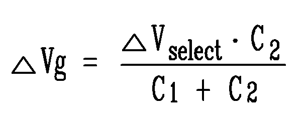
여기서, △Vg는 제 1 캐패시터(C1)와 제 2 캐패시터(C2)의 커플링에 의해 증가하는 제 1 캐패시터(M1)의 게이트의 전압값, △Vselect는 선택신호의 전압폭을 나타낸다. DELTA Vg denotes the voltage value of the gate of the first capacitor M1 that is increased by the coupling of the first capacitor C1 and the second capacitor C2, and DELTA V select represents the voltage width of the selection signal.
그리고, 발광소자(OLED)에 흐르는 전류는 다음의 수학식 5와 같다. The current flowing through the light emitting element OLED is expressed by Equation 5 below.

여기서, IOLED는 발광소자(OLED)에 흐르는 전류, Vgs는 제 1 트랜지스터(M1)에 데이터 전류가 흐를때 제 1 트랜지스터(M1)의 소스와 게이트 사이의 전압, △Vg는 제 1 캐패시터(C1)와 제 2 캐패시터(C2)의 커플링에 의해 증가하는 제 1 트랜지스터(M1)의 게이트의 전압값, Vth는 제 1 트랜지스터(M1)의 문턱전압, β는 제 1 트랜지스터(M1)의 이득계수를 나타낸다. 이때, 제 2 캐패시터(C2)에 의해 제 1 트랜지스터(M1)의 게이트에 인가되는 전압이 낮아지게 되어 구동전류의 전류량이 감소하게 되므로 더 큰 데이터전류를 이용할 수 있게 된다. 따라서, 데이터선에 기입되는 속도를 더욱 빠르게 할 수 있다. Here, I OLED is a current flowing through the light emitting device OLED, Vgs is a voltage between the source and gate of the first transistor M1 when a data current flows in the first transistor M1, and ΔVg is the first capacitor C1. ), The voltage value of the gate of the first transistor M1 increased by the coupling of the second capacitor C2, Vth is the threshold voltage of the first transistor M1, β is the gain coefficient of the first transistor M1 Indicates. At this time, the voltage applied to the gate of the first transistor M1 is lowered by the second capacitor C2, so that the amount of current of the driving current is reduced, so that a larger data current can be used. Therefore, the speed of writing to the data line can be further increased.
그리고, 도 9에 도시되어 있는 것과 같이 화소를 N 모스 트랜지스터로 구현할 수 있으며, 이때 신호는 도 7에 도시된 파형을 반전하여 입력한다. In addition, as illustrated in FIG. 9, the pixel may be implemented with an N MOS transistor, and the signal is inputted by inverting the waveform shown in FIG. 7.
도 10은 본 발명에 따른 발광 표시장치의 제 3 실시예의 구조를 나타내는 구조도이다. 도 10을 참조하여 설명하면, 화소부(100)의 양측면 중 하나의 측면에 주사구동부의 하나의 구성부분인 주사신호발생부(310)를 형성하고 반대편 측면에 발광제어신호발생부(320)를 형성하여 발광표시장치가 좌우대칭이 되도록 형성할 수 있다. 그리고, 하나의 주사구동부(300)에 주사신호발생부와 발광제어신호발생부가 형성되면, 발광표시장치가 좌우대칭이 되도록 하기 위해 주사구동부가 형성되어 있는 측면의 반대측면에 더미공간을 형성한다. 이러한 경우 주사신호발생부와 발광제어신호발생부가 하나의 주사구동부에 형성되어 주사구동부의 크기는 주사신호발생부 또는 발광제어신호발생부 보다 더 크게 형성되게 되어 화소부의 양측면의 공간이 크게 형성된다. 10 is a structural diagram showing a structure of a third embodiment of a light emitting display device according to the present invention. Referring to FIG. 10, the
따라서, 주사신호발생부를 한쪽 측면에 형성하고 발광제어신호발생부를 반대편 측면에 형성되도록 하면, 화소부의 양측면에 형성되는 공간을 줄일 수 있게 되어 발광표시장치의 크기를 줄일 수 있게 된다. Therefore, if the scan signal generator is formed on one side and the light emission control signal generator is formed on the opposite side, the space formed on both sides of the pixel portion can be reduced, thereby reducing the size of the light emitting display device.
도 11은 발광표시장치에 깜빡임을 육안으로 관찰한 결과를 도시한 그래프를 나타낸다. 도 11을 참조하여 설명하면, 한 프레임구간에서 발광시간을 이용하여 휘도를 조절한 것으로 한 프레임 구간에서 한번 발광을 하는 것과 두번 발광을하는 것과 네번 발광을 하는 것을 녹색과 청색을 관찰한 것이다. 11 is a graph illustrating a result of visual observation of flickering in the light emitting display device. Referring to FIG. 11, green and blue are observed to emit light once, emit twice, emit four times, and emit four times in one frame.
깜빡임 정도(Flicker Grade)는 각 발광표시장치의 한번 발광을 하는 것과 두번 발광을 하는 것과 네번 발광을 하는 녹색과 청색을 육안으로 관찰한 것으로 한 구간에서 표 1과 같이 점수를 산정하여 점수를 산정하였다. Flicker Grade is a visual observation of green and blue light emitting each light emitting display device once, two light emission, and four light emission. .
G와 B는 발광표시장치가 녹색만을 표현하거나 청색만을 표현한 것을 나타내며, 펄스 1은 한 프레임구간에서 한번 발광한 것을 나타내며, 펄스 2는 한 프레임구간에서 두번 발광한 것을 나타내며, 펄스 4는 한프레임 구간에서 네번 발광한 것을 나타낸다. G and B indicate that the light emitting display device represents only green color or only blue color,
그리고, 듀티비(Duty Ratio)는 한프레임 구간 내에서 발광기간과 비발광기간의 비를 나타낸 것으로 100%는 한 프레임 전체 시간 동안 발광하는 것이고, 수치가 낮아질수록 비발광기간이 늘어나는 것을 나타낸다. The duty ratio is a ratio of the light emission period and the non-light emission period within one frame period, and 100% indicates that the light emission is performed for the entire time of one frame.
그래프를 보면, 듀티비의 수치가 낮아지도록 하였을때 네번 발광하는 것이 깜빡임 정도가 적게 나타나며 한번을 발광하는 것이 가장 높게 나타난다. 따라서, 한 프레임 구간에서 여러 번 발광하도록 하는 것이 바람직하게 된다. In the graph, when the duty ratio is lowered, four flashes show less flickering and one flash emits the most. Therefore, it is desirable to emit light several times in one frame section.
본 발명의 바람직한 실시예가 특정 용어들을 사용하여 기술되어 왔지만, 그러한 기술은 단지 설명을 하기 위한 것이며, 다음의 청구범위의 기술적 사상 및 범위로부터 이탈되지 않고 여러 가지 변경 및 변화가 가해질 수 있는 것으로 이해되어져야 한다. While preferred embodiments of the present invention have been described using specific terms, such descriptions are for illustrative purposes only and it is understood that various changes and modifications may be made without departing from the spirit and scope of the following claims. You must lose.
본 발명에 따른 발광표시장치 및 발광표시장치 구동방법에 의하면, 발광소자가 한 프레임이 구간 동안 발광하는 시간이 조절되어 발광하는 시간에 따라 발광표시장치의 밝기가 조절되며, 한 프레임의 구간 동안 발광하는 것과 동일한 밝기를 갖도록 하기 위해서는 발광소자에 더 큰 전류가 필요로 하게 되어 데이터선에 전달되는 데이터전류의 전류량을 크게 할 수 있게 된다. 따라서, 데이터전류의 전류량이 커짐에 따라 데이터선에 기입되는 속도를 빠르게 할 수 있다.According to the light emitting display device and the method of driving the light emitting display device according to the present invention, the light emitting device is controlled to emit light during one frame, and thus the brightness of the light emitting display device is adjusted according to the light emitting time. In order to have the same brightness as that of the light emitting device, a larger current is required for the light emitting device, thereby increasing the amount of current of the data current transmitted to the data line. Therefore, as the current amount of the data current increases, the speed of writing to the data line can be increased.
또한, 한 프레임이 구간 동안 발광소자가 적어도 두 번 발광하도록 하여 발광소자가 발광하지 않는 구간이 나누어지도록 하여 각각의 발광하지 않는 구간의 길이가 짧아지게 되어 깜빡임 현상이 나타나지 않게 된다. In addition, the light emitting device emits light at least twice during one frame so that the sections in which the light emitting devices do not emit light are divided so that the length of each non-light emitting section is shortened so that flickering does not occur.
Claims (16)
Priority Applications (4)
| Application Number | Priority Date | Filing Date | Title |
|---|---|---|---|
| KR1020050044696A KR100639007B1 (en) | 2005-05-26 | 2005-05-26 | Light emitting display and driving method thereof |
| JP2005321312A JP2006330664A (en) | 2005-05-26 | 2005-11-04 | Light emitting display device and driving method thereof |
| US11/441,521 US20060267509A1 (en) | 2005-05-26 | 2006-05-26 | Organic light emitting display and driving method thereof |
| CNA2006100927380A CN1941048A (en) | 2005-05-26 | 2006-05-26 | Organic light emitting display and driving method thereof |
Applications Claiming Priority (1)
| Application Number | Priority Date | Filing Date | Title |
|---|---|---|---|
| KR1020050044696A KR100639007B1 (en) | 2005-05-26 | 2005-05-26 | Light emitting display and driving method thereof |
Publications (1)
| Publication Number | Publication Date |
|---|---|
| KR100639007B1 true KR100639007B1 (en) | 2006-10-25 |
Family
ID=37462485
Family Applications (1)
| Application Number | Title | Priority Date | Filing Date |
|---|---|---|---|
| KR1020050044696A KR100639007B1 (en) | 2005-05-26 | 2005-05-26 | Light emitting display and driving method thereof |
Country Status (4)
| Country | Link |
|---|---|
| US (1) | US20060267509A1 (en) |
| JP (1) | JP2006330664A (en) |
| KR (1) | KR100639007B1 (en) |
| CN (1) | CN1941048A (en) |
Cited By (2)
| Publication number | Priority date | Publication date | Assignee | Title |
|---|---|---|---|---|
| KR101898695B1 (en) * | 2012-02-27 | 2018-09-17 | 삼성디스플레이 주식회사 | Organic Light Emitting Display Device and Driving Method Thereof |
| CN112735343A (en) * | 2021-01-04 | 2021-04-30 | 成都中电熊猫显示科技有限公司 | Light-emitting component dimming control method and device and display device |
Families Citing this family (26)
| Publication number | Priority date | Publication date | Assignee | Title |
|---|---|---|---|---|
| JP2007108341A (en) * | 2005-10-12 | 2007-04-26 | Toshiba Matsushita Display Technology Co Ltd | Active matrix type display device |
| JP2008046377A (en) * | 2006-08-17 | 2008-02-28 | Sony Corp | Display device |
| JP5495510B2 (en) | 2007-06-19 | 2014-05-21 | キヤノン株式会社 | Display device and electronic apparatus using the same |
| JP2009014836A (en) * | 2007-07-02 | 2009-01-22 | Canon Inc | Active matrix type display and driving method therefor |
| US20090033601A1 (en) * | 2007-08-02 | 2009-02-05 | Lee Hyo-Jin | Organic light emitting display and its driving method |
| US8497885B2 (en) * | 2007-08-21 | 2013-07-30 | Canon Kabushiki Karsha | Display apparatus and drive method thereof |
| JP2009080272A (en) * | 2007-09-26 | 2009-04-16 | Canon Inc | Active matrix type display device |
| JP2009109641A (en) * | 2007-10-29 | 2009-05-21 | Canon Inc | Driving circuit and active matrix type display device |
| KR101346858B1 (en) * | 2008-11-12 | 2014-01-02 | 엘지디스플레이 주식회사 | Organic electro-luminescence display device |
| KR101056228B1 (en) * | 2009-03-02 | 2011-08-11 | 삼성모바일디스플레이주식회사 | Organic light emitting display |
| JP5284198B2 (en) * | 2009-06-30 | 2013-09-11 | キヤノン株式会社 | Display device and driving method thereof |
| JP2011013415A (en) * | 2009-07-01 | 2011-01-20 | Canon Inc | Active matrix type display apparatus |
| JP2011028135A (en) * | 2009-07-29 | 2011-02-10 | Canon Inc | Display device and driving method of the same |
| TWI421835B (en) | 2010-05-10 | 2014-01-01 | Au Optronics Corp | Organic light emitting display and driving method of the same |
| KR101223488B1 (en) * | 2010-05-11 | 2013-01-17 | 삼성디스플레이 주식회사 | Organic Light Emitting Display and Driving Method Thereof |
| CN101916533B (en) * | 2010-05-19 | 2013-04-17 | 友达光电股份有限公司 | Organic light emitting display and drive method thereof |
| CN102708787A (en) * | 2011-08-25 | 2012-10-03 | 京东方科技集团股份有限公司 | Active matrix organic light emitting diode (AMOLED) pixel unit driving circuit and method, pixel unit and display device |
| CN102708786B (en) * | 2011-08-25 | 2014-12-10 | 京东方科技集团股份有限公司 | Active matrix organic light emitting diode (AMOLED) pixel unit driving circuit and method, pixel unit and display device |
| JP6124573B2 (en) | 2011-12-20 | 2017-05-10 | キヤノン株式会社 | Display device |
| CN102708798B (en) * | 2012-04-28 | 2015-05-13 | 京东方科技集团股份有限公司 | Pixel unit driving circuit, driving method, pixel unit and display device |
| TW201352059A (en) * | 2012-06-15 | 2013-12-16 | Chunghwa Picture Tubes Ltd | Driving circuit of an organic light emitting device and method of operating a driving circuit of an organic light emitting device |
| KR102031763B1 (en) * | 2013-01-11 | 2019-10-16 | 삼성디스플레이 주식회사 | Organic light emitting display device |
| KR102290613B1 (en) * | 2015-06-30 | 2021-08-19 | 엘지디스플레이 주식회사 | Organic Light Emitting Display And Driving Method Thereof |
| KR20180082698A (en) * | 2017-01-10 | 2018-07-19 | 삼성디스플레이 주식회사 | Display device and driving method thereof |
| CN107909967B (en) * | 2017-12-11 | 2021-04-09 | 成都晶砂科技有限公司 | Driving method and driving circuit capable of selecting working area of driving tube |
| TWI644303B (en) * | 2017-12-12 | 2018-12-11 | 友達光電股份有限公司 | Driving method for display device |
Citations (4)
| Publication number | Priority date | Publication date | Assignee | Title |
|---|---|---|---|---|
| JPH08248925A (en) * | 1995-03-10 | 1996-09-27 | Sharp Corp | Electronic equipment |
| KR20020077005A (en) * | 2001-03-30 | 2002-10-11 | 가부시키가이샤 히타치세이사쿠쇼 | Display device and driving method thereof |
| KR20040042867A (en) * | 2002-11-14 | 2004-05-20 | 가부시키가이샤 한도오따이 에네루기 켄큐쇼 | Display device and driving method of the same |
| KR20050052263A (en) * | 2003-11-29 | 2005-06-02 | 삼성에스디아이 주식회사 | Display panel, light emitting display device using the panel and driving method thereof |
Family Cites Families (22)
| Publication number | Priority date | Publication date | Assignee | Title |
|---|---|---|---|---|
| JPH113048A (en) * | 1997-06-10 | 1999-01-06 | Canon Inc | Electroluminescent element and device and their production |
| JP4092857B2 (en) * | 1999-06-17 | 2008-05-28 | ソニー株式会社 | Image display device |
| JP4727029B2 (en) * | 1999-11-29 | 2011-07-20 | 株式会社半導体エネルギー研究所 | EL display device, electric appliance, and semiconductor element substrate for EL display device |
| JP2001210122A (en) * | 2000-01-28 | 2001-08-03 | Matsushita Electric Ind Co Ltd | Luminaire, video display device, method of driving video display device, liquid crystal display panel, method of manufacturing liquid crystal display panel, method of driving liquid crystal display panel, array substrate, display device, viewfinder and video camera |
| JP2002251167A (en) * | 2001-02-26 | 2002-09-06 | Sanyo Electric Co Ltd | Display device |
| US6661180B2 (en) * | 2001-03-22 | 2003-12-09 | Semiconductor Energy Laboratory Co., Ltd. | Light emitting device, driving method for the same and electronic apparatus |
| JP4785300B2 (en) * | 2001-09-07 | 2011-10-05 | 株式会社半導体エネルギー研究所 | Electrophoretic display device, display device, and electronic device |
| EP1434193A4 (en) * | 2001-09-07 | 2009-03-25 | Panasonic Corp | El display, el display driving circuit and image display |
| JP2003150104A (en) * | 2001-11-15 | 2003-05-23 | Matsushita Electric Ind Co Ltd | Method for driving el display device, and el display device and information display device |
| JP4251801B2 (en) * | 2001-11-15 | 2009-04-08 | パナソニック株式会社 | EL display device and driving method of EL display device |
| KR100702103B1 (en) * | 2002-04-26 | 2007-04-02 | 도시바 마쯔시따 디스플레이 테크놀로지 컴퍼니, 리미티드 | El display device drive method |
| JP4357413B2 (en) * | 2002-04-26 | 2009-11-04 | 東芝モバイルディスプレイ株式会社 | EL display device |
| JP4195337B2 (en) * | 2002-06-11 | 2008-12-10 | 三星エスディアイ株式会社 | Light emitting display device, display panel and driving method thereof |
| CN100504975C (en) * | 2002-12-19 | 2009-06-24 | 株式会社半导体能源研究所 | Driving method of light emitting device and electronic apparatus |
| JP2004279990A (en) * | 2003-03-19 | 2004-10-07 | Toshiba Matsushita Display Technology Co Ltd | El display device |
| JP2004294752A (en) * | 2003-03-27 | 2004-10-21 | Toshiba Matsushita Display Technology Co Ltd | El display device |
| JPWO2004100118A1 (en) * | 2003-05-07 | 2006-07-13 | 東芝松下ディスプレイテクノロジー株式会社 | EL display device and driving method thereof |
| JP2004361816A (en) * | 2003-06-06 | 2004-12-24 | Toshiba Matsushita Display Technology Co Ltd | El display device |
| JP2005055726A (en) * | 2003-08-06 | 2005-03-03 | Toshiba Matsushita Display Technology Co Ltd | El display device |
| KR100514183B1 (en) * | 2003-09-08 | 2005-09-13 | 삼성에스디아이 주식회사 | Pixel driving circuit and method for organic electroluminescent display |
| JP2005122076A (en) * | 2003-10-20 | 2005-05-12 | Toshiba Matsushita Display Technology Co Ltd | El display device |
| KR100515305B1 (en) * | 2003-10-29 | 2005-09-15 | 삼성에스디아이 주식회사 | Light emitting display device and display panel and driving method thereof |
-
2005
- 2005-05-26 KR KR1020050044696A patent/KR100639007B1/en not_active IP Right Cessation
- 2005-11-04 JP JP2005321312A patent/JP2006330664A/en active Pending
-
2006
- 2006-05-26 CN CNA2006100927380A patent/CN1941048A/en active Pending
- 2006-05-26 US US11/441,521 patent/US20060267509A1/en not_active Abandoned
Patent Citations (4)
| Publication number | Priority date | Publication date | Assignee | Title |
|---|---|---|---|---|
| JPH08248925A (en) * | 1995-03-10 | 1996-09-27 | Sharp Corp | Electronic equipment |
| KR20020077005A (en) * | 2001-03-30 | 2002-10-11 | 가부시키가이샤 히타치세이사쿠쇼 | Display device and driving method thereof |
| KR20040042867A (en) * | 2002-11-14 | 2004-05-20 | 가부시키가이샤 한도오따이 에네루기 켄큐쇼 | Display device and driving method of the same |
| KR20050052263A (en) * | 2003-11-29 | 2005-06-02 | 삼성에스디아이 주식회사 | Display panel, light emitting display device using the panel and driving method thereof |
Cited By (2)
| Publication number | Priority date | Publication date | Assignee | Title |
|---|---|---|---|---|
| KR101898695B1 (en) * | 2012-02-27 | 2018-09-17 | 삼성디스플레이 주식회사 | Organic Light Emitting Display Device and Driving Method Thereof |
| CN112735343A (en) * | 2021-01-04 | 2021-04-30 | 成都中电熊猫显示科技有限公司 | Light-emitting component dimming control method and device and display device |
Also Published As
| Publication number | Publication date |
|---|---|
| US20060267509A1 (en) | 2006-11-30 |
| CN1941048A (en) | 2007-04-04 |
| JP2006330664A (en) | 2006-12-07 |
Similar Documents
| Publication | Publication Date | Title |
|---|---|---|
| KR100639007B1 (en) | Light emitting display and driving method thereof | |
| JP4188930B2 (en) | Luminescent display device | |
| KR100592646B1 (en) | Light Emitting Display and Driving Method Thereof | |
| JP4630789B2 (en) | Light emitting display device and pixel circuit | |
| KR100666549B1 (en) | AMOLED and Driving method thereof | |
| KR100688798B1 (en) | Light Emitting Display and Driving Method Thereof | |
| JP5844525B2 (en) | Pixel, organic light emitting display device and driving method thereof | |
| KR100673760B1 (en) | Light emitting display | |
| KR100515351B1 (en) | Display panel, light emitting display device using the panel and driving method thereof | |
| US20040150595A1 (en) | Electro-optical device, method of driving electro-optical device, and electronic apparatus | |
| KR20120009904A (en) | Pixel and Organic Light Emitting Display Device Using the Same | |
| KR100600346B1 (en) | Light emitting display | |
| KR20050046469A (en) | Pixel circuit in display device and driving method thereof | |
| KR20060064683A (en) | Display apparatus having active matrix display panel, and method for driving the same | |
| KR100600345B1 (en) | Pixel circuit and light emitting display using the same | |
| CN112785969A (en) | Electroluminescent display panel with light emitting drive circuit | |
| KR100688799B1 (en) | Light emitting display, and method for driving light emitting display and pixel circuit | |
| KR100600344B1 (en) | Pixel circuit and light emitting display | |
| KR100589382B1 (en) | Display panel, light emitting display device using the panel and driving method thereof | |
| KR100722113B1 (en) | Light emitting display | |
| KR100595108B1 (en) | Pixel and Light Emitting Display and Driving Method Thereof | |
| KR100947992B1 (en) | Pixel and organic light emitting display device using the same | |
| KR100581808B1 (en) | Light emitting display by using demultiplexer | |
| KR100592645B1 (en) | Pixel and Driving Method of Light Emitting Display Using the Same | |
| KR100688804B1 (en) | Light emitting display and dirving method thereof |
Legal Events
| Date | Code | Title | Description |
|---|---|---|---|
| A201 | Request for examination | ||
| E701 | Decision to grant or registration of patent right | ||
| GRNT | Written decision to grant | ||
| FPAY | Annual fee payment |
Payment date: 20121008 Year of fee payment: 7 |
|
| FPAY | Annual fee payment |
Payment date: 20130930 Year of fee payment: 8 |
|
| FPAY | Annual fee payment |
Payment date: 20141001 Year of fee payment: 9 |
|
| FPAY | Annual fee payment |
Payment date: 20150930 Year of fee payment: 10 |
|
| LAPS | Lapse due to unpaid annual fee |