JP2005055726A - El display device - Google Patents
El display device Download PDFInfo
- Publication number
- JP2005055726A JP2005055726A JP2003287297A JP2003287297A JP2005055726A JP 2005055726 A JP2005055726 A JP 2005055726A JP 2003287297 A JP2003287297 A JP 2003287297A JP 2003287297 A JP2003287297 A JP 2003287297A JP 2005055726 A JP2005055726 A JP 2005055726A
- Authority
- JP
- Japan
- Prior art keywords
- current
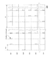
- transistor
- pixel
- signal line
- voltage
- Prior art date
- Legal status (The legal status is an assumption and is not a legal conclusion. Google has not performed a legal analysis and makes no representation as to the accuracy of the status listed.)
- Pending
Links
- 239000011159 matrix material Substances 0.000 claims abstract description 25
- 230000008859 change Effects 0.000 claims description 270
- 238000000034 method Methods 0.000 description 581
- 238000005401 electroluminescence Methods 0.000 description 531
- 235000019557 luminance Nutrition 0.000 description 242
- 238000010586 diagram Methods 0.000 description 163
- 230000002829 reductive effect Effects 0.000 description 137
- 239000010408 film Substances 0.000 description 121
- 239000003990 capacitor Substances 0.000 description 116
- 238000004364 calculation method Methods 0.000 description 98
- 239000000758 substrate Substances 0.000 description 90
- 230000000875 corresponding effect Effects 0.000 description 86
- 230000001276 controlling effect Effects 0.000 description 85
- 238000012545 processing Methods 0.000 description 80
- 230000008569 process Effects 0.000 description 69
- 230000015572 biosynthetic process Effects 0.000 description 55
- 238000006243 chemical reaction Methods 0.000 description 49
- 230000014509 gene expression Effects 0.000 description 49
- 230000015556 catabolic process Effects 0.000 description 48
- 238000005516 engineering process Methods 0.000 description 47
- 229910021420 polycrystalline silicon Inorganic materials 0.000 description 47
- 229920005591 polysilicon Polymers 0.000 description 47
- 230000003071 parasitic effect Effects 0.000 description 46
- 230000006870 function Effects 0.000 description 43
- 239000010409 thin film Substances 0.000 description 43
- 238000009826 distribution Methods 0.000 description 36
- 238000012546 transfer Methods 0.000 description 35
- 239000003086 colorant Substances 0.000 description 34
- 230000007423 decrease Effects 0.000 description 34
- 230000000694 effects Effects 0.000 description 33
- 239000010410 layer Substances 0.000 description 27
- 238000007789 sealing Methods 0.000 description 27
- 239000000463 material Substances 0.000 description 26
- 238000007726 management method Methods 0.000 description 23
- XUIMIQQOPSSXEZ-UHFFFAOYSA-N Silicon Chemical compound [Si] XUIMIQQOPSSXEZ-UHFFFAOYSA-N 0.000 description 21
- 229910052710 silicon Inorganic materials 0.000 description 21
- 239000010703 silicon Substances 0.000 description 21
- 239000004973 liquid crystal related substance Substances 0.000 description 20
- 239000004065 semiconductor Substances 0.000 description 20
- 229910052751 metal Inorganic materials 0.000 description 19
- 239000002184 metal Substances 0.000 description 19
- 230000003247 decreasing effect Effects 0.000 description 15
- 230000001681 protective effect Effects 0.000 description 15
- 238000003860 storage Methods 0.000 description 15
- 229910021417 amorphous silicon Inorganic materials 0.000 description 14
- 239000012071 phase Substances 0.000 description 14
- 238000013461 design Methods 0.000 description 12
- 230000009467 reduction Effects 0.000 description 12
- 238000001514 detection method Methods 0.000 description 11
- 238000004519 manufacturing process Methods 0.000 description 11
- 238000003672 processing method Methods 0.000 description 11
- 239000011347 resin Substances 0.000 description 11
- 229920005989 resin Polymers 0.000 description 11
- 230000005540 biological transmission Effects 0.000 description 10
- 239000011521 glass Substances 0.000 description 10
- 230000031700 light absorption Effects 0.000 description 10
- 229910052782 aluminium Inorganic materials 0.000 description 9
- XAGFODPZIPBFFR-UHFFFAOYSA-N aluminium Chemical compound [Al] XAGFODPZIPBFFR-UHFFFAOYSA-N 0.000 description 9
- 238000012937 correction Methods 0.000 description 9
- 239000006185 dispersion Substances 0.000 description 9
- 230000000717 retained effect Effects 0.000 description 9
- 230000002195 synergetic effect Effects 0.000 description 9
- 230000008901 benefit Effects 0.000 description 8
- 238000007667 floating Methods 0.000 description 8
- 238000003780 insertion Methods 0.000 description 8
- 230000037431 insertion Effects 0.000 description 8
- 230000035515 penetration Effects 0.000 description 8
- 238000002474 experimental method Methods 0.000 description 7
- 230000033001 locomotion Effects 0.000 description 7
- 239000007769 metal material Substances 0.000 description 7
- 230000002093 peripheral effect Effects 0.000 description 7
- 230000000630 rising effect Effects 0.000 description 7
- 238000004804 winding Methods 0.000 description 7
- HEZMWWAKWCSUCB-PHDIDXHHSA-N (3R,4R)-3,4-dihydroxycyclohexa-1,5-diene-1-carboxylic acid Chemical compound O[C@@H]1C=CC(C(O)=O)=C[C@H]1O HEZMWWAKWCSUCB-PHDIDXHHSA-N 0.000 description 6
- OKTJSMMVPCPJKN-UHFFFAOYSA-N Carbon Chemical compound [C] OKTJSMMVPCPJKN-UHFFFAOYSA-N 0.000 description 6
- 238000000137 annealing Methods 0.000 description 6
- 229910052799 carbon Inorganic materials 0.000 description 6
- 230000007547 defect Effects 0.000 description 6
- 238000009792 diffusion process Methods 0.000 description 6
- 238000000605 extraction Methods 0.000 description 6
- 238000005224 laser annealing Methods 0.000 description 6
- 230000007257 malfunction Effects 0.000 description 6
- 238000012986 modification Methods 0.000 description 6
- 230000004048 modification Effects 0.000 description 6
- 239000000049 pigment Substances 0.000 description 6
- 230000004044 response Effects 0.000 description 6
- 230000001052 transient effect Effects 0.000 description 6
- 230000003044 adaptive effect Effects 0.000 description 5
- 230000020169 heat generation Effects 0.000 description 5
- 230000001678 irradiating effect Effects 0.000 description 5
- 238000010030 laminating Methods 0.000 description 5
- 238000005070 sampling Methods 0.000 description 5
- 230000001360 synchronised effect Effects 0.000 description 5
- 238000002834 transmittance Methods 0.000 description 5
- VYZAMTAEIAYCRO-UHFFFAOYSA-N Chromium Chemical compound [Cr] VYZAMTAEIAYCRO-UHFFFAOYSA-N 0.000 description 4
- 241001475178 Dira Species 0.000 description 4
- PEDCQBHIVMGVHV-UHFFFAOYSA-N Glycerine Chemical compound OCC(O)CO PEDCQBHIVMGVHV-UHFFFAOYSA-N 0.000 description 4
- 101100309620 Schizosaccharomyces pombe (strain 972 / ATCC 24843) sck2 gene Proteins 0.000 description 4
- BQCADISMDOOEFD-UHFFFAOYSA-N Silver Chemical compound [Ag] BQCADISMDOOEFD-UHFFFAOYSA-N 0.000 description 4
- 238000013459 approach Methods 0.000 description 4
- 229910052804 chromium Inorganic materials 0.000 description 4
- 239000011651 chromium Substances 0.000 description 4
- 230000002596 correlated effect Effects 0.000 description 4
- 238000005520 cutting process Methods 0.000 description 4
- 230000006866 deterioration Effects 0.000 description 4
- 238000011156 evaluation Methods 0.000 description 4
- 239000010931 gold Substances 0.000 description 4
- 230000003287 optical effect Effects 0.000 description 4
- 230000002441 reversible effect Effects 0.000 description 4
- 238000000926 separation method Methods 0.000 description 4
- 229910052709 silver Inorganic materials 0.000 description 4
- 239000004332 silver Substances 0.000 description 4
- LXMSZDCAJNLERA-ZHYRCANASA-N spironolactone Chemical compound C([C@@H]1[C@]2(C)CC[C@@H]3[C@@]4(C)CCC(=O)C=C4C[C@H]([C@@H]13)SC(=O)C)C[C@@]21CCC(=O)O1 LXMSZDCAJNLERA-ZHYRCANASA-N 0.000 description 4
- 208000026082 sterile multifocal osteomyelitis with periostitis and pustulosis Diseases 0.000 description 4
- 230000000007 visual effect Effects 0.000 description 4
- LYCAIKOWRPUZTN-UHFFFAOYSA-N Ethylene glycol Chemical compound OCCO LYCAIKOWRPUZTN-UHFFFAOYSA-N 0.000 description 3
- PXHVJJICTQNCMI-UHFFFAOYSA-N Nickel Chemical compound [Ni] PXHVJJICTQNCMI-UHFFFAOYSA-N 0.000 description 3
- 101100420795 Schizosaccharomyces pombe (strain 972 / ATCC 24843) sck1 gene Proteins 0.000 description 3
- 230000002159 abnormal effect Effects 0.000 description 3
- NIXOWILDQLNWCW-UHFFFAOYSA-N acrylic acid group Chemical group C(C=C)(=O)O NIXOWILDQLNWCW-UHFFFAOYSA-N 0.000 description 3
- 239000000853 adhesive Substances 0.000 description 3
- 230000001070 adhesive effect Effects 0.000 description 3
- 239000012790 adhesive layer Substances 0.000 description 3
- 230000002411 adverse Effects 0.000 description 3
- 229910045601 alloy Inorganic materials 0.000 description 3
- 239000000956 alloy Substances 0.000 description 3
- 239000013078 crystal Substances 0.000 description 3
- 239000002274 desiccant Substances 0.000 description 3
- 238000007599 discharging Methods 0.000 description 3
- 239000000975 dye Substances 0.000 description 3
- 230000005684 electric field Effects 0.000 description 3
- PCHJSUWPFVWCPO-UHFFFAOYSA-N gold Chemical compound [Au] PCHJSUWPFVWCPO-UHFFFAOYSA-N 0.000 description 3
- 229910052737 gold Inorganic materials 0.000 description 3
- 230000006872 improvement Effects 0.000 description 3
- 230000001788 irregular Effects 0.000 description 3
- 239000003550 marker Substances 0.000 description 3
- 238000002156 mixing Methods 0.000 description 3
- 239000011368 organic material Substances 0.000 description 3
- 238000003825 pressing Methods 0.000 description 3
- 230000035945 sensitivity Effects 0.000 description 3
- XOLBLPGZBRYERU-UHFFFAOYSA-N tin dioxide Chemical compound O=[Sn]=O XOLBLPGZBRYERU-UHFFFAOYSA-N 0.000 description 3
- 238000009966 trimming Methods 0.000 description 3
- 239000004925 Acrylic resin Substances 0.000 description 2
- 229920000178 Acrylic resin Polymers 0.000 description 2
- 239000004593 Epoxy Substances 0.000 description 2
- 229910052770 Uranium Inorganic materials 0.000 description 2
- 206010047571 Visual impairment Diseases 0.000 description 2
- 239000011358 absorbing material Substances 0.000 description 2
- 239000011230 binding agent Substances 0.000 description 2
- JOPOVCBBYLSVDA-UHFFFAOYSA-N chromium(6+) Chemical compound [Cr+6] JOPOVCBBYLSVDA-UHFFFAOYSA-N 0.000 description 2
- 239000011248 coating agent Substances 0.000 description 2
- 238000000576 coating method Methods 0.000 description 2
- 239000002131 composite material Substances 0.000 description 2
- 239000004020 conductor Substances 0.000 description 2
- 238000012217 deletion Methods 0.000 description 2
- 230000037430 deletion Effects 0.000 description 2
- 230000009977 dual effect Effects 0.000 description 2
- 230000005611 electricity Effects 0.000 description 2
- 239000007772 electrode material Substances 0.000 description 2
- 238000005538 encapsulation Methods 0.000 description 2
- 239000003822 epoxy resin Substances 0.000 description 2
- 210000000744 eyelid Anatomy 0.000 description 2
- 229910052732 germanium Inorganic materials 0.000 description 2
- GNPVGFCGXDBREM-UHFFFAOYSA-N germanium atom Chemical compound [Ge] GNPVGFCGXDBREM-UHFFFAOYSA-N 0.000 description 2
- 238000009499 grossing Methods 0.000 description 2
- 230000012447 hatching Effects 0.000 description 2
- 210000003128 head Anatomy 0.000 description 2
- 230000017525 heat dissipation Effects 0.000 description 2
- 239000002346 layers by function Substances 0.000 description 2
- 229910052744 lithium Inorganic materials 0.000 description 2
- 238000011068 loading method Methods 0.000 description 2
- 239000011777 magnesium Substances 0.000 description 2
- 230000014759 maintenance of location Effects 0.000 description 2
- 238000005259 measurement Methods 0.000 description 2
- 238000003909 pattern recognition Methods 0.000 description 2
- 229920000647 polyepoxide Polymers 0.000 description 2
- 239000002356 single layer Substances 0.000 description 2
- 239000007787 solid Substances 0.000 description 2
- 239000007790 solid phase Substances 0.000 description 2
- 230000003068 static effect Effects 0.000 description 2
- 239000000126 substance Substances 0.000 description 2
- 230000001629 suppression Effects 0.000 description 2
- 230000002123 temporal effect Effects 0.000 description 2
- 229910052727 yttrium Inorganic materials 0.000 description 2
- RICKKZXCGCSLIU-UHFFFAOYSA-N 2-[2-[carboxymethyl-[[3-hydroxy-5-(hydroxymethyl)-2-methylpyridin-4-yl]methyl]amino]ethyl-[[3-hydroxy-5-(hydroxymethyl)-2-methylpyridin-4-yl]methyl]amino]acetic acid Chemical compound CC1=NC=C(CO)C(CN(CCN(CC(O)=O)CC=2C(=C(C)N=CC=2CO)O)CC(O)=O)=C1O RICKKZXCGCSLIU-UHFFFAOYSA-N 0.000 description 1
- 229910000838 Al alloy Inorganic materials 0.000 description 1
- 229910001148 Al-Li alloy Inorganic materials 0.000 description 1
- JBRZTFJDHDCESZ-UHFFFAOYSA-N AsGa Chemical compound [As]#[Ga] JBRZTFJDHDCESZ-UHFFFAOYSA-N 0.000 description 1
- 238000012935 Averaging Methods 0.000 description 1
- 208000013586 Complex regional pain syndrome type 1 Diseases 0.000 description 1
- RYGMFSIKBFXOCR-UHFFFAOYSA-N Copper Chemical compound [Cu] RYGMFSIKBFXOCR-UHFFFAOYSA-N 0.000 description 1
- 102100040844 Dual specificity protein kinase CLK2 Human genes 0.000 description 1
- LFQSCWFLJHTTHZ-UHFFFAOYSA-N Ethanol Chemical compound CCO LFQSCWFLJHTTHZ-UHFFFAOYSA-N 0.000 description 1
- PXGOKWXKJXAPGV-UHFFFAOYSA-N Fluorine Chemical compound FF PXGOKWXKJXAPGV-UHFFFAOYSA-N 0.000 description 1
- GYHNNYVSQQEPJS-UHFFFAOYSA-N Gallium Chemical compound [Ga] GYHNNYVSQQEPJS-UHFFFAOYSA-N 0.000 description 1
- 229910001218 Gallium arsenide Inorganic materials 0.000 description 1
- 108010010803 Gelatin Proteins 0.000 description 1
- 241000587161 Gomphocarpus Species 0.000 description 1
- 101000749291 Homo sapiens Dual specificity protein kinase CLK2 Proteins 0.000 description 1
- 241001237160 Kallima inachus Species 0.000 description 1
- WHXSMMKQMYFTQS-UHFFFAOYSA-N Lithium Chemical compound [Li] WHXSMMKQMYFTQS-UHFFFAOYSA-N 0.000 description 1
- FYYHWMGAXLPEAU-UHFFFAOYSA-N Magnesium Chemical compound [Mg] FYYHWMGAXLPEAU-UHFFFAOYSA-N 0.000 description 1
- 206010027146 Melanoderma Diseases 0.000 description 1
- 229910000861 Mg alloy Inorganic materials 0.000 description 1
- 229910001182 Mo alloy Inorganic materials 0.000 description 1
- 241000255969 Pieris brassicae Species 0.000 description 1
- 239000004743 Polypropylene Substances 0.000 description 1
- 229910019336 PrMnO3 Inorganic materials 0.000 description 1
- GWEVSGVZZGPLCZ-UHFFFAOYSA-N Titan oxide Chemical compound O=[Ti]=O GWEVSGVZZGPLCZ-UHFFFAOYSA-N 0.000 description 1
- RTAQQCXQSZGOHL-UHFFFAOYSA-N Titanium Chemical compound [Ti] RTAQQCXQSZGOHL-UHFFFAOYSA-N 0.000 description 1
- 239000000980 acid dye Substances 0.000 description 1
- 230000003213 activating effect Effects 0.000 description 1
- 239000001000 anthraquinone dye Substances 0.000 description 1
- 238000000149 argon plasma sintering Methods 0.000 description 1
- 239000000987 azo dye Substances 0.000 description 1
- 239000011324 bead Substances 0.000 description 1
- 230000002457 bidirectional effect Effects 0.000 description 1
- 230000004397 blinking Effects 0.000 description 1
- 230000000903 blocking effect Effects 0.000 description 1
- 239000005018 casein Substances 0.000 description 1
- BECPQYXYKAMYBN-UHFFFAOYSA-N casein, tech. Chemical compound NCCCCC(C(O)=O)N=C(O)C(CC(O)=O)N=C(O)C(CCC(O)=N)N=C(O)C(CC(C)C)N=C(O)C(CCC(O)=O)N=C(O)C(CC(O)=O)N=C(O)C(CCC(O)=O)N=C(O)C(C(C)O)N=C(O)C(CCC(O)=N)N=C(O)C(CCC(O)=N)N=C(O)C(CCC(O)=N)N=C(O)C(CCC(O)=O)N=C(O)C(CCC(O)=O)N=C(O)C(COP(O)(O)=O)N=C(O)C(CCC(O)=N)N=C(O)C(N)CC1=CC=CC=C1 BECPQYXYKAMYBN-UHFFFAOYSA-N 0.000 description 1
- 235000021240 caseins Nutrition 0.000 description 1
- 230000000295 complement effect Effects 0.000 description 1
- 229910052802 copper Inorganic materials 0.000 description 1
- 239000010949 copper Substances 0.000 description 1
- 230000008878 coupling Effects 0.000 description 1
- 238000010168 coupling process Methods 0.000 description 1
- 238000005859 coupling reaction Methods 0.000 description 1
- 230000006378 damage Effects 0.000 description 1
- 230000002950 deficient Effects 0.000 description 1
- 238000006731 degradation reaction Methods 0.000 description 1
- 238000000151 deposition Methods 0.000 description 1
- 238000009795 derivation Methods 0.000 description 1
- 239000003599 detergent Substances 0.000 description 1
- 230000002542 deteriorative effect Effects 0.000 description 1
- 239000010432 diamond Substances 0.000 description 1
- 229910003460 diamond Inorganic materials 0.000 description 1
- 238000005553 drilling Methods 0.000 description 1
- 238000004043 dyeing Methods 0.000 description 1
- 239000000284 extract Substances 0.000 description 1
- 238000001914 filtration Methods 0.000 description 1
- FWQHNLCNFPYBCA-UHFFFAOYSA-N fluoran Chemical compound C12=CC=CC=C2OC2=CC=CC=C2C11OC(=O)C2=CC=CC=C21 FWQHNLCNFPYBCA-UHFFFAOYSA-N 0.000 description 1
- 239000011737 fluorine Substances 0.000 description 1
- 229910052731 fluorine Inorganic materials 0.000 description 1
- 239000011888 foil Substances 0.000 description 1
- 230000004927 fusion Effects 0.000 description 1
- 229910052733 gallium Inorganic materials 0.000 description 1
- 229920000159 gelatin Polymers 0.000 description 1
- 239000008273 gelatin Substances 0.000 description 1
- 235000019322 gelatine Nutrition 0.000 description 1
- 235000011852 gelatine desserts Nutrition 0.000 description 1
- 239000001046 green dye Substances 0.000 description 1
- 230000005525 hole transport Effects 0.000 description 1
- 238000003384 imaging method Methods 0.000 description 1
- 229910052738 indium Inorganic materials 0.000 description 1
- APFVFJFRJDLVQX-UHFFFAOYSA-N indium atom Chemical compound [In] APFVFJFRJDLVQX-UHFFFAOYSA-N 0.000 description 1
- 229910010272 inorganic material Inorganic materials 0.000 description 1
- 239000011147 inorganic material Substances 0.000 description 1
- 238000009413 insulation Methods 0.000 description 1
- 239000011229 interlayer Substances 0.000 description 1
- 238000003475 lamination Methods 0.000 description 1
- 239000007788 liquid Substances 0.000 description 1
- 229910052749 magnesium Inorganic materials 0.000 description 1
- 239000000203 mixture Substances 0.000 description 1
- 239000000025 natural resin Substances 0.000 description 1
- 229910052759 nickel Inorganic materials 0.000 description 1
- 239000011022 opal Substances 0.000 description 1
- 238000000059 patterning Methods 0.000 description 1
- 230000000149 penetrating effect Effects 0.000 description 1
- 230000035699 permeability Effects 0.000 description 1
- ISWSIDIOOBJBQZ-UHFFFAOYSA-N phenol group Chemical group C1(=CC=CC=C1)O ISWSIDIOOBJBQZ-UHFFFAOYSA-N 0.000 description 1
- 239000005011 phenolic resin Substances 0.000 description 1
- 230000001443 photoexcitation Effects 0.000 description 1
- IEQIEDJGQAUEQZ-UHFFFAOYSA-N phthalocyanine Chemical compound N1C(N=C2C3=CC=CC=C3C(N=C3C4=CC=CC=C4C(=N4)N3)=N2)=C(C=CC=C2)C2=C1N=C1C2=CC=CC=C2C4=N1 IEQIEDJGQAUEQZ-UHFFFAOYSA-N 0.000 description 1
- 239000001007 phthalocyanine dye Substances 0.000 description 1
- 238000007747 plating Methods 0.000 description 1
- 229920006289 polycarbonate film Polymers 0.000 description 1
- 229920000728 polyester Polymers 0.000 description 1
- 229920006267 polyester film Polymers 0.000 description 1
- 229920001721 polyimide Polymers 0.000 description 1
- 238000006116 polymerization reaction Methods 0.000 description 1
- -1 polypropylene Polymers 0.000 description 1
- 229920001155 polypropylene Polymers 0.000 description 1
- 238000002360 preparation method Methods 0.000 description 1
- 230000005855 radiation Effects 0.000 description 1
- 239000001044 red dye Substances 0.000 description 1
- 230000004043 responsiveness Effects 0.000 description 1
- 239000000565 sealant Substances 0.000 description 1
- 239000002210 silicon-based material Substances 0.000 description 1
- 238000005476 soldering Methods 0.000 description 1
- 230000007480 spreading Effects 0.000 description 1
- 238000003892 spreading Methods 0.000 description 1
- 238000004544 sputter deposition Methods 0.000 description 1
- 230000000087 stabilizing effect Effects 0.000 description 1
- 239000000057 synthetic resin Substances 0.000 description 1
- 229920003002 synthetic resin Polymers 0.000 description 1
- 238000012360 testing method Methods 0.000 description 1
- 229910001887 tin oxide Inorganic materials 0.000 description 1
- 239000010936 titanium Substances 0.000 description 1
- 229910052719 titanium Inorganic materials 0.000 description 1
- OGIDPMRJRNCKJF-UHFFFAOYSA-N titanium oxide Inorganic materials [Ti]=O OGIDPMRJRNCKJF-UHFFFAOYSA-N 0.000 description 1
- 239000005341 toughened glass Substances 0.000 description 1
- 230000007704 transition Effects 0.000 description 1
- AAAQKTZKLRYKHR-UHFFFAOYSA-N triphenylmethane Chemical compound C1=CC=CC=C1C(C=1C=CC=CC=1)C1=CC=CC=C1 AAAQKTZKLRYKHR-UHFFFAOYSA-N 0.000 description 1
- 229910052721 tungsten Inorganic materials 0.000 description 1
- 238000007740 vapor deposition Methods 0.000 description 1
Images


Abstract
Description
本発明は、有機または無機エレクトロルミネッセンス(EL)素子を用いたEL表示パネルなどの自発光表示パネルに関するものである。また、これらの表示パネルなどの駆動回路(IC)に関するものである。EL表示パネルなどの駆動方法と駆動回路およびそれらを用いた情報表示装置などに関するものである。 The present invention relates to a self-luminous display panel such as an EL display panel using an organic or inorganic electroluminescence (EL) element. The present invention also relates to a drive circuit (IC) such as these display panels. The present invention relates to a driving method and a driving circuit for an EL display panel and the like, an information display device using them, and the like.
一般に、アクティブマトリクス型表示装置では、多数の画素をマトリクス状に並べ、与えられた映像信号に応じて画素毎に光強度を制御することによって画像を表示する。たとえば、電気光学物質として液晶を用いた場合は、各画素に書き込まれる電圧に応じて画素の透過率が変化する。電気光学変換物質として有機エレクトロルミネッセンス(EL)材料を用いたアクティブマトリクス型の画像表示装置は画素に書き込まれる電流に応じて発光輝度が変化する。 In general, in an active matrix display device, an image is displayed by arranging a large number of pixels in a matrix and controlling the light intensity for each pixel in accordance with a given video signal. For example, when liquid crystal is used as the electro-optical material, the transmittance of the pixel changes according to the voltage written to each pixel. In an active matrix image display device using an organic electroluminescence (EL) material as an electro-optic conversion substance, light emission luminance changes according to a current written to a pixel.
液晶表示パネルは、各画素はシャッタとして動作し、バックライトからの光を画素であるシャッタでオンオフさせることにより画像を表示する。有機EL表示パネルは各画素に発光素子を有する自発光型である。そのため、有機EL表示パネルは、液晶表示パネルに比べて画像の視認性が高い、バックライトが不要、応答速度が速い等の利点を有する。 In the liquid crystal display panel, each pixel operates as a shutter, and an image is displayed by turning on and off light from a backlight with a shutter that is a pixel. The organic EL display panel is a self-luminous type having a light emitting element in each pixel. Therefore, the organic EL display panel has advantages such as higher image visibility than the liquid crystal display panel, no backlight, and high response speed.
有機EL表示パネルは各発光素子(画素)の輝度は電流量によって制御される。つまり、発光素子が電流駆動型あるいは電流制御型であるという点で液晶表示パネルとは大きく異なる。 In the organic EL display panel, the luminance of each light emitting element (pixel) is controlled by the amount of current. That is, it is greatly different from the liquid crystal display panel in that the light emitting element is a current drive type or a current control type.
有機EL表示パネルも単純マトリクス方式とアクティブマトリクス方式の構成が可能である。前者は構造が単純であるものの大型かつ高精細の表示パネルの実現が困難である。しかし、安価である。後者は大型、高精細表示パネルを実現できる。しかし、制御方法が技術的に難しい、比較的高価であるという課題がある。現在では、アクティブマトリクス方式の開発が盛んに行われている。アクティブマトリクス方式は、各画素に設けた発光素子に流れる電流を画素内部に設けた薄膜トランジスタ(トランジスタ)によって制御する。 The organic EL display panel can also be configured in a simple matrix system and an active matrix system. Although the former has a simple structure, it is difficult to realize a large and high-definition display panel. However, it is cheap. The latter can realize a large, high-definition display panel. However, there is a problem that the control method is technically difficult and relatively expensive. At present, active matrix systems are actively developed. In the active matrix system, a current flowing through a light emitting element provided in each pixel is controlled by a thin film transistor (transistor) provided in the pixel.
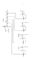
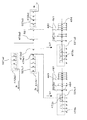
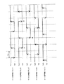
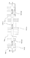
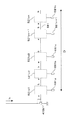
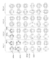
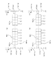
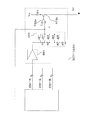
このアクティブマトリクス方式の有機EL表示パネルの一画素分の等価回路を図46に示す(たとえば、特許文献1参照)。画素16は発光素子であるEL素子15、第1のトランジスタ11a、第2のトランジスタ11bおよび蓄積容量19からなる。発光素子15は有機エレクトロルミネッセンス(EL)素子である。本発明では、EL素子15に電流を供給(制御)するトランジスタ11aを駆動用トランジスタ11と呼ぶ。また、図46のトランジスタ11bのように、スイッチとして動作するトランジスタをスイッチ用トランジスタ11と呼ぶ。
An equivalent circuit for one pixel of this active matrix organic EL display panel is shown in FIG. 46 (see, for example, Patent Document 1). The
有機EL素子15は多くの場合、整流性があるため、OLED(有機発光ダイオード)と呼ばれることがある。図46などでは発光素子15としてダイオードの記号を用いている。
Since the
ただし、本発明における発光素子15はOLEDに限るものではなく、素子15に流れる電流量によって輝度が制御されるものであればよい。たとえば、無機EL素子が例示される。その他、半導体で構成される白色発光ダイオードが例示される。また、一般的な発光ダイオードが例示される。その他、発光トランジスタでもよい。また、発光素子15は必ずしも整流性が要求されるものではない。双方向性ダイオードであってもよい。本発明のEL素子15はこのいずれでもよい。
However, the
図46の例では、Pチャンネル型のトランジスタ11aのソース端子(S)をVdd(電源電位)とし、EL素子15のカソード(陰極)は接地電位(Vss)に接続される。一方、アノード(陽極)はトランジスタ11bのドレイン端子(D)に接続されている。一方、Pチャンネル型のトランジスタ11aのゲート端子はゲート信号線17aに接続され、ソース端子はソース信号線18に接続され、ドレイン端子は蓄積容量19およびトランジスタ11aのゲート端子(G)に接続されている。
In the example of FIG. 46, the source terminal (S) of the P-
画素16を動作させるために、まず、ゲート信号線17aを選択状態とし、ソース信号線18に輝度情報を表す映像信号を印加する。すると、トランジスタ11aが導通し、蓄積容量19が充電又は放電され、トランジスタ11bのゲート電位は映像信号の電位に一致する。ゲート信号線17aを非選択状態とすると、トランジスタ11aがオフになり、トランジスタ11bは電気的にソース信号線18から切り離される。しかし、トランジスタ11aのゲート電位は蓄積容量(コンデンサ)19によって安定に保持される。トランジスタ11aを介して発光素子15に流れる電流は、トランジスタ11aのゲート/ソース端子間電圧Vgsに応じた値となり、発光素子15はトランジスタ11aを通って供給される電流量に応じた輝度で発光し続ける。
液晶表示パネルは、自発光デバイスではないため、バックライトを用いないと画像を表示できないという問題点がある。バックライトを構成するためには所定の厚みが必要であるため、表示パネルの厚みが厚くなるという問題があった。また、液晶表示パネルでカラー表示を行うためには、カラーフィルターを使用する必要がある。そのため、光利用効率が低いという問題点があった。また、色再現範囲が狭いという問題点があった。 Since the liquid crystal display panel is not a self-luminous device, there is a problem that an image cannot be displayed unless a backlight is used. Since a predetermined thickness is required to configure the backlight, there is a problem that the thickness of the display panel is increased. In order to perform color display on the liquid crystal display panel, it is necessary to use a color filter. Therefore, there is a problem that the light utilization efficiency is low. There is also a problem that the color reproduction range is narrow.
有機EL表示パネルは、低温ポリシリコントランジスタアレイを用いてパネルを構成する。しかし、有機EL素子は、電流により発光するため、トランジスタの特性にバラツキがあると、表示ムラが発生するという課題があった。 The organic EL display panel is configured by using a low-temperature polysilicon transistor array. However, since the organic EL element emits light by current, there is a problem that display unevenness occurs when the transistor characteristics vary.
表示ムラは、画素を電流プログラム方式の構成を採用することにより低減することが可能である。電流プログラムを実施するためには、電流駆動方式のドライバ回路が必要である。しかし、電流駆動方式のドライバ回路にも電流出力段を構成するトランジスタ素子にバラツキが発生する。そのため、各出力端子からの階調出力電流にバラツキが発生し、良好な画像表示ができないという課題があった。 Display unevenness can be reduced by adopting a current programming system for the pixels. In order to implement the current program, a current drive type driver circuit is required. However, variation also occurs in the transistor elements constituting the current output stage in the current drive type driver circuit. For this reason, there is a problem in that the gradation output current from each output terminal varies and a good image display cannot be performed.
この目的を達成するために本発明のEL表示パネル(EL表示装置)のドライバ回路は、単位電流を出力する複数のトランジスタを具備し、このトランジスタの個数を変化させることにより出力電流を出力するものである。また、多段のカレントミラー回路で構成されたことを特徴としている。信号の受け渡しが電圧受け渡しとなるトランジスタ群は密に形成し、カレントミラー回路の群との信号の受け渡しは、電流受け渡しの構成を採用する。また、基準電流は、複数のトランジスタで行う。 In order to achieve this object, the driver circuit of the EL display panel (EL display device) of the present invention includes a plurality of transistors that output unit current, and outputs output current by changing the number of transistors. It is. Further, it is characterized by being composed of a multi-stage current mirror circuit. A transistor group in which signal transfer is voltage transfer is formed densely, and signal transfer with the current mirror circuit group adopts a current transfer configuration. The reference current is performed by a plurality of transistors.
本発明のソースドライバ回路は、カントミラー回路を構成するトランジスタが隣接するように形成しているので、しきい値のずれによる出力電流のばらつきが小さく。したがって、EL表示パネルの輝度むらの発生を抑制することが可能となり、その実用的効果は大きい。 Since the source driver circuit of the present invention is formed so that the transistors constituting the cant mirror circuit are adjacent to each other, variation in output current due to a shift in threshold value is small. Therefore, it is possible to suppress the occurrence of luminance unevenness in the EL display panel, and its practical effect is great.
また、本発明の表示パネル、表示装置等は、高画質、良好な動画表示性能、低消費電力、低コスト化、高輝度化等のそれぞれの構成に応じて特徴ある効果を発揮する。 In addition, the display panel, the display device, and the like of the present invention exhibit distinctive effects according to their respective configurations such as high image quality, good moving image display performance, low power consumption, low cost, and high luminance.
なお、本発明を用いれば、低消費電力の情報表示装置などを構成できるので、電力を消費しない。また、小型軽量化できるので、資源を消費しない。また、高精細の表示パネルであっても十分に対応できる。したがって、地球環境、宇宙環境に優しいこととなる。 Note that if the present invention is used, a low power consumption information display device or the like can be configured, so that power is not consumed. Moreover, since it can be reduced in size and weight, resources are not consumed. Further, even a high-definition display panel can be sufficiently handled. Therefore, it is friendly to the global environment and space environment.
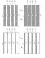
本明細書において各図面は理解を容易にまたは/および作図を容易にするため、省略または/および拡大縮小した箇所がある。たとえば、図11に図示する表示パネルの断面図では薄膜封止膜111などを十分厚く図示している。一方、図10において、封止フタ85は薄く図示している。また、省略した箇所もある。たとえば、本発明の表示パネルなどでは、反射防止のために円偏光板などの位相フィルムが必要である。しかし、本明細書の各図面では省略している。以上のことは以下の図面に対しても同様である。また、同一番号または、記号等を付した箇所は同一もしくは類似の形態もしくは材料あるいは機能もしくは動作を有する。
In the present specification, each drawing is omitted or / and enlarged or reduced for easy understanding and / or drawing. For example, in the cross-sectional view of the display panel shown in FIG. 11, the thin
なお、各図面等で説明した内容は特に断りがなくとも、他の実施例等と組み合わせることができる。たとえば、図8の表示パネルにタッチパネルなどを付加し、図157、図159から図161に図示する情報表示装置とすることができる。また、拡大レンズ1582を取り付け、ビデオカメラ(図159など参照のこと)などに用いるビューファインダ(図58を参照のこと)を構成することもできる。
Note that the contents described in the drawings and the like can be combined with other embodiments and the like without particular notice. For example, a touch panel or the like is added to the display panel of FIG. 8, and the information display device illustrated in FIGS. 157 and 159 to 161 can be obtained. Further, a viewfinder (see FIG. 58) used for a video camera (see FIG. 159, etc.) can be configured by attaching a
また、図4、図15、図18、図21、図23、図29、図30、図35、図36、図40、図41、図44、図100〜図110、図125〜図131、図133〜図146、図197〜図205、図234〜図244、図255〜図264、図276〜図302、図327〜図336、図355〜図358、図362〜図373、図381~図384、図386、図396〜図398、図404〜図406などで説明した本発明の駆動方法は、いずれの本発明の表示装置または表示パネルに適用することができる。 4, 15, 18, 21, 23, 29, 30, 35, 36, 40, 41, 44, 100 to 110, 125 to 131, 133 to 146, 197 to 205, 234 to 244, 255 to 264, 276 to 302, 327 to 336, 355 to 358, 362 to 373, and 381 The driving method of the present invention described in FIGS. 384, 386, 396 to 398, and 404 to 406 can be applied to any display device or display panel of the present invention.
なお、本明細書では、駆動用トランジスタ11、スイッチング用トランジスタ11は薄膜トランジスタとして説明するが、これに限定するものではない。薄膜ダイオード(TFD)、リングダイオードなどでも構成することができる。また、薄膜素子に限定するものではなく、シリコンウエハに形成したトランジスタでもものでもよい。基板71をシリコンウエハで形成すればよい。もちろん、FET、MOS−FET、MOSトランジスタ、バイポーラトランジスタでもよい。これらも基本的に薄膜トランジスタである。その他、バリスタ、サイリスタ、リングダイオード、ホトダオード、ホトトランジスタ、PLZT素子などでもよいことは言うまでもない。つまり、本発明のトランジスタ素子11、ゲートドライバ回路12、ソースドライバ回路14などは、これらのいずれでも使用することができる。
Note that in this specification, the driving
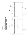
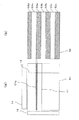
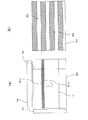
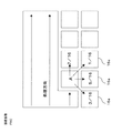
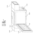
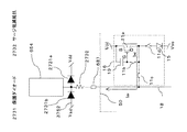
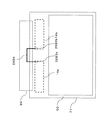
以下、本発明のELパネルについて図面を参照しながら説明をする。有機EL表示パネルは、図10に示すように、画素電極としての透明電極105が形成されたガラス板71(アレイ基板)上に、電子輸送層、発光層、正孔輸送層などからなる少なくとも1層の有機機能層(EL層)15、及び金属電極(反射膜)(カソード)106が積層されたものである。透明電極(画素電極)105である陽極(アノード)にプラス、金属電極(反射電極)106の陰極(カソード)にマイナスの電圧を加え、すなわち、透明電極105及び金属電極106間に直流を印加することにより、有機機能層(EL層)15が発光する。
Hereinafter, the EL panel of the present invention will be described with reference to the drawings. As shown in FIG. 10, the organic EL display panel includes at least one of an electron transport layer, a light emitting layer, a hole transport layer, and the like on a glass plate 71 (array substrate) on which a
金属電極106には、リチウム、銀、アルミニウム、マグネシウム、インジウム、銅または各々の合金等の仕事関数が小さなものを用いることが好ましい。特に、例えばAl−Li合金を用いることが好ましい。また、透明電極105には、ITO等の仕事関数の大きな導電性材料または金等を用いることができる。なお、金を電極材料として用いた場合、電極は半透明の状態となる。なお、ITOはIZOなどの他の材料でもよい。この事項は他の画素電極105に対しても同様である。
The
なお、封止フタ85とアレイ基板71との空間には乾燥剤107を配置する。これは、有機EL膜15は湿度に弱いためである。乾燥剤107によりシール剤を浸透する水分を吸収し有機EL膜15の劣化を防止する。
A
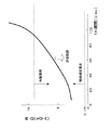
EL表示パネル(EL表示装置)の課題として、パネル内部で発生するハレーションを原因とするコントラスト低下がある。EL素子15(画素16)から発生した光がパネル内部に閉じ込められ乱反射するために発生する。 A problem of an EL display panel (EL display device) is a reduction in contrast caused by halation occurring inside the panel. This occurs because light generated from the EL element 15 (pixel 16) is confined within the panel and diffusely reflected.
この課題を解決するために、本発明では、図388に図示するように、画像表示に非有効な表示領域(無効領域)に光吸収膜3881を形成または配置している。光吸収膜3881を形成することにより、画素16から発生した光(光の軌跡3882で示す)が基板71などで乱反射し、発生するハレーションによる表示コントラスト低下を抑制することができる。
In order to solve this problem, in the present invention, as shown in FIG. 388, a
なお、無効領域とは、基板71あるいはフタ85の側面、基板71かつ表示領域以外(たとえば、ゲートドライバ12が形成された領域など)、フタ85の全面(下取り出しの場合)などである。
Note that the invalid area includes the side surface of the
図388に図示するように、基板71内で乱反射する光3883が光吸収膜3881で吸収される。封止フタ85を黒色材料などで形成することも有効である。
As illustrated in FIG. 388, light 3883 that is irregularly reflected in the
図388(a)はパネル端部を斜め形状に形成あるいは構成している。斜め形状に形成あるいは構成することにより光吸収膜3881の形成面積を広くすることができる。したがって、パネルの基板71内でハレーションする光(光の軌跡3882)を効率より吸収することができ、表示コントラストを向上できる。
In FIG. 388 (a), the end of the panel is formed or configured in an oblique shape. The formation area of the
光吸収膜を構成する物質としては、アクリル樹脂などの有機材料にカーボンを含有させたもの、黒色の色素あるいは顔料を有機樹脂中に分散させたもの、カラーフィルターの様にゼラチンやカゼインを黒色の酸性染料で染色したものが例示される。その他、単一で黒色となるフルオラン系色素を発色させて用いたものでもよく、緑色系色素と赤色系色素とを混合した配色ブラックを用いることもできる。また、スパッタにより形成されたPrMnO3膜、プラズマ重合により形成されたフタロシアニン膜等が例示される。 Substances that make up the light absorption film include organic materials such as acrylic resins containing carbon, black pigments or pigments dispersed in organic resins, and gelatin or casein as a color filter. What was dye | stained with the acid dye is illustrated. In addition, a single black fluoran dye may be used, and a color scheme black obtained by mixing a green dye and a red dye may also be used. Examples thereof include a PrMnO3 film formed by sputtering and a phthalocyanine film formed by plasma polymerization.
以上の材料はすべて黒色の材料であるが、光吸収膜としては、表示素子が発生する光色に対し、補色の関係の材料を用いても良い。例えば、カラーフィルター用の光吸収材料を望ましい光吸収特性が得られるように改良して用いれば良い。基本的には前記した黒色吸収材料と同様に、色素を用いて天然樹脂を染色したものを用いても良い。また、色素を合成樹脂中に分散した材料を用いることができる。色素の選択の範囲は黒色色素よりもむしろ幅広く、アゾ染料、アントラキノン染料、フタロシアニン染料、トリフェニルメタン染料などから適切な1種、もしくはそれらのうち2種類以上の組み合わせでも良い。 The above materials are all black materials, but as the light absorption film, a material having a complementary color with respect to the light color generated by the display element may be used. For example, a light-absorbing material for a color filter may be used so as to obtain desired light absorption characteristics. Basically, a material obtained by dyeing a natural resin with a pigment may be used in the same manner as the black absorbing material described above. Further, a material in which a pigment is dispersed in a synthetic resin can be used. The selection range of the pigment is wider than the black pigment, and may be one suitable from azo dye, anthraquinone dye, phthalocyanine dye, triphenylmethane dye, or a combination of two or more thereof.
また、光吸収膜としては金属材料を用いてもよい。たとえば、六価クロムが例示される。六価クロムは黒色であり、光吸収膜として機能する。その他、オパールガラス、酸化チタンなどの光散乱材料であってもよい。光を散乱させることにより、結果的に光を吸収することと等価になるからである。 Further, a metal material may be used as the light absorption film. For example, hexavalent chromium is exemplified. Hexavalent chromium is black and functions as a light absorbing film. In addition, light scattering materials such as opal glass and titanium oxide may be used. This is because scattering the light is equivalent to absorbing the light as a result.
以上の事項は、図11などの構成にも適用することができることは言うまでもない。 Needless to say, the above items can also be applied to the configuration of FIG.
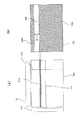
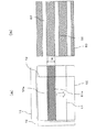
図10はガラスのフタ85を用いて封止する構成であるが、図11のようにフィルム(薄膜でもよい。つまり、薄膜封止膜である)111を用いた封止であってもよい。たとえば、封止フィルム(薄膜封止膜)111としては電解コンデンサのフィルムにDLC(ダイヤモンド ライク カーボン)を蒸着したものを用いることが例示される。このフィルムは水分浸透性が極めて悪い(防湿性能が高い)。このフィルムを封止膜111として用いる。また、DLC(ダイヤモンド ライク カーボン)膜などを電極106の表面に直接蒸着する構成ものよいことは言うまでもない。その他、樹脂薄膜と金属薄膜を多層に積層して、薄膜封止膜を構成してもよい。
FIG. 10 shows a configuration in which sealing is performed using a
薄膜の膜厚はn・d(nは薄膜の屈折率、複数の薄膜が積層されている場合はそれらの屈折率を総合(各薄膜のn・dを計算)にして計算する。dは薄膜の膜厚、複数の薄膜が積層されている場合はそれらの屈折率を総合して計算する。)が、EL素子15の発光主波長λ以下となるようにするとよい。この条件を満足させることにより、EL素子15からの光取り出し効率が、ガラス基板で封止した場合に比較して2倍以上になる。また、アルミニウムと銀の合金あるいは混合物あるいは積層物を形成してもよい。
The film thickness of the thin film is calculated by n · d (where n is the refractive index of the thin film, and when a plurality of thin films are stacked, the refractive indexes thereof are combined (calculate n · d of each thin film)). When the plurality of thin films are laminated, their refractive indexes are calculated together.) Is preferably equal to or less than the emission main wavelength λ of the
以上のようにフタ85を用いず、封止膜111で封止する構成を薄膜封止と呼ぶ。基板71側から光を取り出す「下取り出し(図10を参照、光取り出し方向は図10の矢印方向である)」の場合の薄膜封止は、EL膜を形成後、EL膜上にカソードとなるアルミ電極を形成する。次にこのアルミ膜上に緩衝層としての樹脂層を形成する。緩衝層としては、アクリル、エポキシなどの有機材料が例示される。また、膜厚は1μm以上10μm以下の厚みが適する。さらに好ましくは、膜厚は2μm以上6μm以下の厚みが適する。この緩衝膜上の封止膜74を形成する。緩衝膜がないと、応力によりEL膜の構造が崩れ、筋状に欠陥が発生する。封止膜111は前述したように、DLC(ダイヤモンド ライク カーボン)、あるいは電界コンデンサの層構造(誘電体薄膜とアルミ薄膜とを交互に多層蒸着した構造)が例示される。
A configuration in which sealing is performed with the sealing
EL層15側から光を取り出す「上取り出し図11を参照、光取り出し方向は図11の矢印方向である」の場合の薄膜封止は、EL膜15を形成後、EL膜15上にカソード(アノード)となるAg−Mg膜を20オングストローム以上300オングストロームの膜厚で形成する。その上に、ITOなどの透明電極を形成して低抵抗化する。次にこの電極膜上に緩衝層としての樹脂層を形成する。この緩衝膜上に封止膜111を形成する。
In the case of extracting light from the
有機EL層15から発生した光の半分は、反射膜106で反射され、アレイ基板71と透過して出射される。しかし、反射膜106には外光を反射し写り込みが発生して表示コントラストを低下させる。この対策のために、アレイ基板71にλ/4板108および偏光板(偏光フィルム)109を配置している。これらは一般的に円偏光板(円偏光シート)と呼ばれる。
Half of the light generated from the
なお、画素が反射電極の場合はEL層15から発生した光は上方向に出射される。したがって、位相板108および偏光板109は光出射側に配置することはいうまでもない。なお、反射型画素は、画素電極105を、アルミニウム、クロム、銀などで構成して得られる。また、画素電極105の表面に、凸部(もしくは凹凸部)を設けることで有機EL層15との界面が広くなり発光面積が大きくなり、また、発光効率が向上する。なお、カソード106(アノード105)となる反射膜を透明電極に形成する、あるいは反射率を30%以下に低減できる場合は、円偏光板は不要である。写り込みが大幅に減少するからである。また、光の干渉も低減し望ましい。
When the pixel is a reflective electrode, the light generated from the
トランジスタ11はLDD(lightly doped drain)構造を採用することが好ましい。また、本明細書ではEL素子として有機EL素子(OEL、PEL、PLED、OLEDなど多種多様な略称で記述される)15を例にあげて説明するがこれに限定するものではなく、無機EL素子にも適用されることは言うまでもない。
The
まず、有機EL表示パネルに用いられるアクティブマトリックス方式は、
特定の画素を選択し、必要な表示情報を与えられること。
1フレーム期間を通じてEL素子に電流を流すことができることという2つの条件を満足させなければならない。
First, the active matrix method used for organic EL display panels is:
A specific pixel can be selected and given display information can be given.
Two conditions must be satisfied that current can flow through the EL element throughout one frame period.
この2つの条件を満足させるため、図46に図示する従来の有機ELの画素構成では、第1のトランジスタ11bは画素を選択するためのスイッチング用トランジスタ、第2のトランジスタ11aはEL素子(EL膜)15に電流を供給するための駆動用トランジスタとする。
In order to satisfy these two conditions, in the conventional organic EL pixel configuration shown in FIG. 46, the
この構成を用いて階調を表示させる場合、駆動用トランジスタ11aのゲート電圧として階調に応じた電圧を印加する必要がある。したがって、駆動用トランジスタ11aのオン電流のばらつきがそのまま表示に現れる。
In the case of displaying gradation using this configuration, it is necessary to apply a voltage corresponding to the gradation as the gate voltage of the driving
トランジスタのオン電流は単結晶で形成されたトランジスタであれば、きわめて均一であるが、安価なガラス基板に形成することのできる形成温度が450度以下の低温ポリシリ技術で形成した低温多結晶トタンジスタでは、そのしきい値のばらつきが±0.2V〜0.5Vの範囲でばらつきがある。そのため、駆動用トランジスタ11aを流れるオン電流がこれに対応してばらつき、表示にムラが発生する。これらのムラは、しきい値電圧のばらつきのみならず、トランジスタの移動度、ゲート絶縁膜の厚みなどでも発生する。また、トランジスタ11の劣化によっても特性は変化する。
The on-current of a transistor is very uniform if it is a transistor formed of a single crystal, but in a low-temperature polycrystalline transistor formed by low-temperature polysilicon technology that can be formed on an inexpensive glass substrate with a formation temperature of 450 degrees or less. The threshold value varies in the range of ± 0.2V to 0.5V. For this reason, the on-current flowing through the driving
この現象は、低温ポリシリコン技術に限定されるものではなく、プロセス温度が450度(摂氏)以上の高温ポリシリコン技術でも、固相(CGS)成長させた半導体膜を用いてトランジスタなどを形成したものでも発生する。その他、有機トランジスタでも発生する。アモルファスシリコントランジスタでも発生する。 This phenomenon is not limited to low-temperature polysilicon technology, and transistors and the like are formed using solid-phase (CGS) grown semiconductor films even in high-temperature polysilicon technology with a process temperature of 450 degrees Celsius or higher. Even things can occur. In addition, it occurs in organic transistors. It also occurs in amorphous silicon transistors.
以下に説明する本発明は、これらの技術に対応し、対策できる構成あるいは方式である。なお、本明細書では低温ポリシリコン技術で形成したトランジスタを主として説明する。 The present invention described below is a configuration or method that can cope with these techniques. In this specification, a transistor formed by low-temperature polysilicon technology will be mainly described.
したがって、図46のように、電圧を書き込むことにより、階調を表示させる方法では、均一な表示を得るために、デバイスの特性を厳密に制御する必要がある。しかし、現状の低温多結晶ポリシリコントランジスタなどではこのバラツキを所定範囲以内の抑えるというスペックを満足できない。 Therefore, as shown in FIG. 46, in the method of displaying gradation by writing a voltage, it is necessary to strictly control the device characteristics in order to obtain a uniform display. However, the current low-temperature polycrystalline polysilicon transistor and the like cannot satisfy the specification of suppressing this variation within a predetermined range.
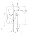
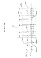
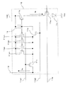
本発明のEL表示装置の画素構造は、具体的には図1に示すように単位画素が最低4つからなる複数のトランジスタ11ならびにEL素子により形成される。画素電極はソース信号線と重なるように構成する。つまり、ソース信号線18上に絶縁膜あるいはアクリル材料からなる平坦化膜を形成して絶縁し、この絶縁膜上に画素電極105を形成する。このようにソース信号線18上の少なくとも1部に画素電極を重ねる構成をハイアパーチャ(HA)構造と呼ぶ。不要な干渉光などが低減し、良好な発光状態が期待できる。
Specifically, the pixel structure of the EL display device of the present invention is formed by a plurality of
ゲート信号線(第1の走査線)17aをアクティブ(ON電圧を印加)とすることによりEL素子15の駆動用のトランジスタ11aおよびスイッチ用トランジスタ11cを通して、前記EL素子15に流すべき電流値をソースドライバ回路14から流す。また、トランジスタ11aのゲートとドレイン間を短絡するようにトランジスタ11bがゲート信号線17aアクティブ(ON電圧を印加)となることにより開くと共に、トランジスタ11aのゲートとソース間に接続されたコンデンサ(キャパシタ、蓄積容量、付加容量)19にトランジスタ11aのゲート電圧(あるいはドレイン電圧)を記憶する(図3(a)を参照のこと)。
By activating the gate signal line (first scanning line) 17a (applying an ON voltage), the current value to be passed through the
なお、コンデンサ(蓄積容量)19の大きさは、0.2pF以上2pF以下とすることがよく、中でもコンデンサ(蓄積容量)19の大きさは、0.4pF以上1.2pF以下とすることがよい。画素サイズを考慮してコンデンサ19の容量を決定する。1画素に必要な容量をCs(pF)とし、1画素が占める面積(開口率ではない)をSp(平方μm)とすれば、500/S ≦ Cs ≦ 20000/Sとし、さらに好ましくは、1000/Sp ≦ Cs ≦ 10000/Spとなるようにする。なお、トランジスタのゲート容量は小さいので、ここでいうQとは、蓄積容量(コンデンサ)19単独の容量である。
Note that the size of the capacitor (storage capacitor) 19 is preferably 0.2 pF or more and 2 pF or less, and in particular, the size of the capacitor (storage capacitor) 19 is preferably 0.4 pF or more and 1.2 pF or less. . The capacitance of the
ゲート信号線17aを非アクティブ(OFF電圧を印加)、ゲート信号線17bをアクティブとして、電流の流れる経路を前記第1のトランジスタ11a並びにEL素子15に接続されたトランジスタ11dならびに前記EL素子15を含む経路に切り替えて、記憶した電流を前記EL素子15に流すように動作する(図3(b)を参照のこと)。
The
この回路は1画素内に4つのトランジスタ11を有しており、トランジスタ11a のゲートはトランジスタ11bのソースに接続されている。また、トランジスタ11bおよびトランジスタ11cのゲートはゲート信号線17aに接続されている。トランジスタ11bのドレインはトランジスタ11cのソースならびにトランジスタ11dのソースに接続され、トランジスタ11cのドレインはソース信号線18に接続されている。トランジスタ11dのゲートはゲート信号線17bに接続され、トランジスタ11dのドレインはEL素子15のアノード電極に接続されている。
This circuit has four
なお、図1ではすべてのトランジスタはPチャンネルで構成している。Pチャンネルは多少Nチャンネルのトランジスタに比較してモビリティが低いが、耐圧が大きくまた劣化も発生しにくいので好ましい。しかし、本発明はEL素子構成をPチャンネルで構成することのみに限定するものではない。Nチャンネルのみで構成してもよい。また、NチャンネルとPチャンネルの両方を用いて構成してもよい。 In FIG. 1, all the transistors are P-channel. The P channel has a lower mobility than an N channel transistor, but is preferable because it has a high breakdown voltage and is less likely to deteriorate. However, the present invention is not limited to the configuration of the EL element with the P channel. You may comprise only N channel. Moreover, you may comprise using both N channel and P channel.
最適には画素を構成するトランジスタ11をすべてPチャンネルで形成し、内蔵ゲートドライバ12もPチャンネルで形成することが好ましい。このようにアレイをPチャンネルのみのトランジスタで形成することにより、マスク枚数が5枚となり、低コスト化、高歩留まり化を実現できる。
Optimally, it is preferable that all the
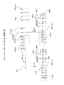
以下、さらに本発明の理解を容易にするために、本発明のEL素子構成について図3を用いて説明する。本発明のEL素子構成は2つのタイミングにより制御される。第1のタイミングは必要な電流値を記憶させるタイミングである。このタイミングでトランジスタ11bならびにトランジスタ11cがONすることにより、等価回路として図3(a)となる。ここで、信号線より所定の電流Iwが書き込まれる。これによりトランジスタ11aはゲートとドレインが接続された状態となり、このトランジスタ11aとトランジスタ11cを通じて電流Iwが流れる。したがって、トランジスタ11aのゲート−ソースの電圧はI1が流れるような電圧となる。
Hereinafter, in order to facilitate the understanding of the present invention, the EL element configuration of the present invention will be described with reference to FIG. The EL device configuration of the present invention is controlled by two timings. The first timing is a timing for storing a necessary current value. When the
第2のタイミングはトランジスタ11aとトランジスタ11cが閉じ、トランジスタ11dが開くタイミングであり、そのときの等価回路は図3(b)となる。トランジスタ11aのソース−ゲート間の電圧は保持されたままとなる。この場合、トランジスタ11aは常に飽和領域で動作するため、Iwの電流は一定となる。
The second timing is a timing at which the
このように動作させると、図5に図示するようになる。つまり、図5(a)の51aは表示画面50における、ある時刻での電流プログラムされている画素(行)(書き込み画素行)を示している。この画素(行)51aは、図5(b)に図示するように非点灯(非表示画素(行))とする。他の画素(行)は表示画素(行)53とする(表示領域53の画素16のEL素子15には電流が流れ、EL素子15が発光している)。
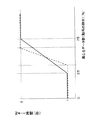
When operated in this way, it is as shown in FIG. That is, 51a in FIG. 5A indicates a pixel (row) (write pixel row) in the
図1の画素構成の場合、図3(a)に示すように、電流プログラム時は、プログラム電流Iwがソース信号線18に流れる。この電流Iwがトランジスタ11aを流れ、Iwを流す電流が保持されるように、コンデンサ19に電圧設定(プログラム)される。このとき、トランジスタ11dはオープン状態(オフ状態)である。
In the case of the pixel configuration of FIG. 1, as shown in FIG. 3A, the program current Iw flows through the
次に、EL素子15に電流を流す期間は図3(b)のように、トランジスタ11c、11bがオフし、トランジスタ11dが動作する。つまり、ゲート信号線17aにオフ電圧(Vgh)が印加され、トランジスタ11b、11cがオフする。一方、ゲート信号線17bにオン電圧(Vgl)が印加され、トランジスタ11dがオンする。
Next, during a period in which a current flows through the
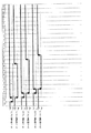
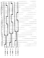
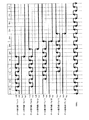
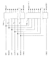
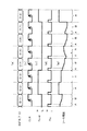
このタイミングチャートを図4に図示する。なお、図4などにおいて、括弧内の添え字(たとえば、(1)など)は画素行の番号を示している。つまり、ゲート信号線17a(1)とは、画素行(1)のゲート信号線17aを示している。また、図4の上段の*H(「*」には任意の記号、数値が当てはまり、水平走査線の番号を示す)とは、水平走査期間を示している。つまり、1Hとは第1番目の水平走査期間である。なお、以上の事項は、説明を容易にするためであって、限定(1Hの番号、1H周期、画素行番号の順番など)するものではない。
This timing chart is shown in FIG. In FIG. 4 and the like, subscripts in parentheses (for example, (1) and the like) indicate pixel row numbers. That is, the
図4でわかるように、各選択された画素行(選択期間は、1Hとしている)において、ゲート信号線17aにオン電圧が印加されている時には、ゲート信号線17bにはオフ電圧が印加されている。また、この期間は、EL素子15には電流が流れていない(非点灯状態)。選択されていない画素行において、ゲート信号線17aにオフ電圧が印加され、ゲート信号線17bにはオン電圧が印加されている。また、この期間は、EL素子15に電流が流れている(点灯状態)。
As can be seen from FIG. 4, when a turn-on voltage is applied to the
なお、トランジスタ11aのゲートとトランジスタ11cのゲートは同一のゲート信号線11aに接続している。しかし、トランジスタ11aのゲートとトランジスタ11cのゲートとを異なるゲート信号線11に接続してもよい(図32を参照のこと)。1画素のゲート信号線は3本となる(図1の構成は2本である)。トランジスタ11bのゲートのON/OFFタイミングとトランジスタ11cのゲートのON/OFFタイミングを個別に制御することにより、トランジスタ11aのばらつきによるEL素子15の電流値バラツキをさらに低減することができる。
Note that the gate of the
ゲート信号線17aとゲート信号線17bとを共通にし、トランジスタ11cと11dが異なった導電型(NチャンネルとPチャンネル)とすると、駆動回路の簡略化、ならびに画素の開口率を向上させることが出来る。
When the
このように構成すれば本発明の動作タイミングとしては信号線からの書きこみ経路がオフになる。すなわち所定の電流が記憶される際に、電流の流れる経路に分岐があると正確な電流値がトランジスタ11aのソース(S)−ゲート(G)間容量(コンデンサ)に記憶されない。トランジスタ11cとトランジスタ11dを異なった導電形にすることにより、お互いの閾値を制御することによって走査線の切り替わりのタイミングで必ずトランジスタ11cがオフしたのちに、トランジスタ11dがオンすることが可能になる。
With this configuration, the write path from the signal line is turned off as the operation timing of the present invention. That is, when a predetermined current is stored, if there is a branch in the current flow path, an accurate current value is not stored in the capacitance (capacitor) between the source (S) and the gate (G) of the
ただし、この場合お互いの閾値を正確にコントロールする必要があるのでプロセスの注意が必要である。なお、以上述べた回路は最低4つのトランジスタで実現可能であるが、より正確なタイミングのコントロールあるいは後述するように、ミラー効果低減のためにトランジスタ11eを図2に示すように、カスケード接続してトランジスタの総数が4以上になっても動作原理は同じである。このようにトランジスタ11eを加えた構成とすることにより、トランジスタ11cを介してプログラムした電流がより精度よくEL素子15に流すことができるようになる。
In this case, however, it is necessary to carefully control each other's thresholds, so care must be taken in the process. Although the circuit described above can be realized with at least four transistors, the
なお、本発明の画素構成は図1、図2の構成に限定されるものではない。たとえば、図113のように構成してもよい。図113は、図1の構成に比較してスイッチ素子11dがない。替わりに切り替えスイッチ1131が形成または配置されている。図1のスイッチ11dは駆動用トランジスタ11aからEL素子15に流れる電流をオンオフ(流す、流さない)制御する機能を有する。以降の実施例でも説明をするが、本発明はこのトランジスタ11dのオンオフ制御機能が重要な構成要素である。トランジスタ11dを形成せず、オンオフ機能を実現するのが、図113の構成である。
Note that the pixel configuration of the present invention is not limited to the configurations of FIGS. For example, it may be configured as shown in FIG. 113 does not have the
図113において、切り替えスイッチ1131のa端子は、アノード電圧Vddに接続されている。なお、a端子に印加する電圧はアノード電圧Vddに限定されるものではなく、EL素子15に流れる電流をオフできる電圧であればいずれでもよい。
In FIG. 113, the terminal a of the
切り替えスイッチ1131のb端子は、カソード電圧(図113ではグランドと図示している)に接続されている。なお、b端子に印加する電圧はカソード電圧に限定されるものではなく、EL素子15に流れる電流をオンできる電圧であればいずれでもよい。
The b terminal of the
切り替えスイッチ1131のc端子にはEL素子15のカソード端子が接続されている。なお、切り替えスイッチ1131はEL素子15に流れる電流をオンオフさせる機能を持つものであればいずれでもよい。したがって、図113の形成位置に限定されるものではなく、EL素子15の電流が流れる経路であればいずれでもよい。また、スイッチの機能の限定されるものでもなく、EL素子15に流れる電流をオンオフできればいずれでもよい。つまり、本発明では、EL素子15の電流経路にEL素子15に流す電流をオンオフできるスイッチング手段を具備しればいずれの画素構成でもよい。
The cathode terminal of the
また、オフとは完全に電流が流れない状態を意味するものではない。EL素子15に流れる電流を通常よりも低減できるものであればよい。以上の事項は本発明の他の構成においても同様である。
Further, “off” does not mean a state in which no current flows completely. Any current can be used as long as the current flowing through the
切り替えスイッチ1131は、PチャンネルとNチャンネルのトランジスタを組み合わせることにより容易に実現できるので説明を要さないであろう。たとえば、アナログスイッチを2回路形成すればよい。もちろん、スイッチ1131はEL素子15に流れる電流をオンオフするだけであるから、PチャンネルトランジスタあるいはNチャンネルトランジスタでも形成することができることは言うまでもない。
Since the change-
スイッチ1131がa端子に接続されている時は、EL素子15のカソード端子にVdd電圧が印加される。したがって、駆動用トランジスタ11aのゲート端子Gがいずれの電圧保持状態であってもEL素子15には電流が流れない。したがって、EL素子15は非点灯状態となる。
When the
スイッチ1131がb端子に接続されている時は、EL素子15のカソード端子にGND電圧が印加される。したがって、駆動用トランジスタ11aのゲート端子Gに保持された電圧状態に応じてEL素子15に電流が流れる。したがって、EL素子15は点灯状態となる。
When the
以上のことより図113の画素構成では、駆動用トランジスタ11aとEL素子15間にはスイッチング用トランジスタ11dが形成されていない。しかし、スイッチ1131を制御することによりEL素子15の点灯制御を行うことができる。
From the above, in the pixel configuration of FIG. 113, the switching
図1、図2などの画素構成では、駆動用トランジスタ11aは1画素につき1個である。本発明はこれに限定するものではなく、駆動用トランジスタ11aは1画素に複数個を形成または配置してもよい。図116はその実施例である。図116では1画素に2個の駆動用トランジスタ素子11a1、11a2が形成され、2個の駆動用トランジスタ11a1、11a2のゲート端子は共通のコンデンサ19に接続されている。駆動用トランジスタ11aを複数個形成することにより、プログラムされる電流バラツキが低減するという効果がある。他の構成は、図1などと同様であるので説明を省略する。
In the pixel configuration shown in FIGS. 1 and 2, the number of driving
図1、図2は駆動用トランジスタ11aが出力する電流をEL素子15に流し、前記電流を駆動用トランジスタ11aとEL素子15間に配置されたスイッチング素子11dでオンオフ制御するものであった。しかし、本発明はこれに限定されるものではない。たとえば、図117の構成が例示される。
1 and 2, the current output from the driving
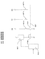
図117の実施例では、EL素子15に流す電流が駆動用トランジスタ11aで制御される。EL素子15に流れる電流をオンオフさせるのはVdd端子とEL素子15間に配置されたスイッチング素子11dで制御される。したがって、本発明はスイッチング素子11dの配置はどこでもよく、EL素子15に流れる電流を制御できるものであればいずれでもよい。動作などは図1などと類似であるので説明を省略する。
In the embodiment of FIG. 117, the current flowing through the
また、図387の画素構成において、すべてのトランジスタはNチャンネルで構成している。しかし、本発明はEL素子構成をNチャンネルで構成することのみに限定するものではない。NチャンネルとPチャンネルの両方を用いて構成してもよい。 Further, in the pixel configuration in FIG. 387, all the transistors are configured by N channels. However, the present invention is not limited to the configuration of the EL element composed of N channels. You may comprise using both N channel and P channel.
以下、図387の画素構成は、2つのタイミングにより制御される。第1のタイミングは必要な電流値を記憶させるタイミングである。 Hereinafter, the pixel configuration in FIG. 387 is controlled by two timings. The first timing is a timing for storing a necessary current value.
このタイミングではゲート信号線17aにオン電圧(Vgh)が印加されることにより、トランジスタ11bならびにトランジスタ11cがONする。また、ゲート信号線17bにオフ電圧(Vgl)が印加され、トランジスタ11dがOFFする。したがって、ソース信号線18より所定の電流Iwが書き込まれる。これによりトランジスタ11aはゲートとドレインが接続された状態となり、このトランジスタ11aとトランジスタ11cを通じてプルグラム電流が流れる。
At this timing, an ON voltage (Vgh) is applied to the
第2のタイミングはゲート信号線17aにオフ電圧が印加され、ゲート信号線17bにオン電圧が印加される。したがって、トランジスタ11aとトランジスタ11cが閉じ、トランジスタ11dが開く。この場合、トランジスタ11aは常に飽和領域で動作するため、Iwの電流は一定となる。
In the second timing, an off voltage is applied to the
トランジスタ11aの特性のバラツキはトランジスタサイズに相関がある。特性バラツキを小さくするため、第1のトランジスタ11aのチャンネル長が5μm以上100μm以下とすることが好ましい。さらに好ましくは、第1のトランジスタ11aのチャンネル長が10μm以上50μm以下とすることが好ましい。これは、チャンネル長Lを長くした場合、チャンネルに含まれる粒界が増えることによって電界が緩和されキンク効果が低く抑えられるためであると考えられる。
The variation in the characteristics of the
以上のように、本発明は、EL素子15に電流が流れこむ経路、またはEL素子15から電流が流れ出す経路(つまり、EL素子15の電流経路である)にEL素子15に流れる電流を制御する回路手段を構成または形成もしくは配置したものである。
As described above, the present invention controls the current flowing through the
電流プログラム方式の1つであるカレントミラー方式であっても、図114に図示すうように、駆動用トランジスタ11bとEL素子15間にスイッチング素子としてのトランジスタ11gを形成または配置することによりEL素子15に流れる電流をオンオフすることができる(制御することができる)。もちろん、トランジスタ11gは図113のスイッチ1131に置き換えても良い。
Even in the current mirror system which is one of current programming systems, as shown in FIG. 114, an EL element is formed by arranging or arranging a transistor 11g as a switching element between the driving
なお、図114のスイッチング用トランジスタ11d、11cは1本のゲート信号線17aに接続されているが、図115に図示するように、トランジスタ11cはゲート信号線17a1で制御し、トランジスタ11dはゲート信号線17a2で制御するように構成してもよい。図115の構成の方が、画素16の制御の汎用性が高くなる。
114 are connected to one
また、図42(a)に図示するように、トランジスタ11b、11cなどはNチャンネルトランジスタで形成してもよい。また、図42(b)に図示するようにトランジスタ11c、11dなどはPチャンネルトランジスタで形成してもよい。
Further, as illustrated in FIG. 42A, the
以上の画素16の構成は、画素16を構成するトランジスタ数が4または5個以上であった。しかし、本発明はこれに限定するものではない。図261に図示するように5個以上のトランジスタで構成してもよい。図261では、駆動用トランジスタ11a1と11a2を用いることにより、低階調領域でも、書込み不足のない電流プログラムを行うことができる。
In the configuration of the
以下、図261に図示した画素構成の駆動方法について説明をする。図261の画素構成は、図265に示すように3つの駆動状態から構成される。第1の状態を図262に示す。また、第2の状態を図263に示す。また、第3の状態を図264に示す。第1の状態と第2の状態が電流プログラムを行っている状態であり、第3の状態がEL素子15に電流を流し、EL素子15が発光している状態である。なお、スイッチ用トランジスタ11d1をオーブンあるいはクローズさせてduty制御を行うことは、本発明の他の実施例と同様であるので説明を省略する。
Hereinafter, a driving method of the pixel configuration illustrated in FIG. 261 will be described. The pixel configuration in FIG. 261 includes three driving states as shown in FIG. The first state is shown in FIG. The second state is shown in FIG. The third state is shown in FIG. The first state and the second state are states in which current programming is performed, and the third state is a state in which a current is passed through the
図261の画素構成はソース信号線18aとソース信号線18bを有している。基本的には、ソース信号線18aに印加するプログラム電流とソース信号線18bに印加するプログラム電流の差が、駆動用トランジスタ11a1に流れるように電流プログラムされ、この電流がEL素子15に流れる。なお、説明を容易にするため、ソース信号線18aにプログラム電流I1=10μA流すとし、ソース信号線18bにプログラム電流I3=10.1μA流し、駆動用トランジスタ11a1にI1とI3の差であるI2=0.1μAを書き込むものとする。
The pixel configuration in FIG. 261 includes a
第1の状態では、図265に示すように、トランジスタ11c2、トランジスタ11b2がクローズ状態にされ、トランジスタd2、トランジスタ11b1、トランジスタ11d1、トランジスタ11c1がオープン状態にされる。 In the first state, as illustrated in FIG. 265, the transistor 11c2 and the transistor 11b2 are closed, and the transistor d2, the transistor 11b1, the transistor 11d1, and the transistor 11c1 are opened.
図262に図示するようにプログラム電流I1はアノード端子から駆動用トランジスタ11a2を介して、ソース信号線18aに流れる。プログラム電流I1はソースドライバIC14により発生させられる。プログラム電流I1はコンデンサ19bにより保持される(駆動用トランジスタ11a2がプログラム電流I1を流せるように駆動用トランジスタ11a2のゲート端子に電圧が保持される)。他のスイッチ用トランジスタ11はオフ状態である。以上の第1の状態により、駆動用トランジスタ11a2は、プログラム電流I1が流れるようにプログラムされる。
As shown in FIG. 262, the program current I1 flows from the anode terminal to the
第2の状態では、図265に示すように、トランジスタ11d2、トランジスタ11b1、トランジスタ11c1がクローズ状態にされ、トランジスタ11c2、トランジスタ11b2、トランジスタ11d1がオープン状態にされる。 In the second state, as illustrated in FIG. 265, the transistor 11d2, the transistor 11b1, and the transistor 11c1 are closed, and the transistor 11c2, the transistor 11b2, and the transistor 11d1 are opened.
図263に図示するように、プログラム電流I3はアノード端子から駆動用トランジスタ11a1を介して、ソース信号線18bに流れる。プログラム電流I3はソースドライバIC14により発生させられる。
As shown in FIG. 263, the program current I3 flows from the anode terminal to the
プログラム電流I3=10.1μAのうち、プログラム電流I1=10μAは駆動用トランジスタ11a2により供給される。したがって、駆動用トランジスタ11a1はプログラム電流I1とI3の差であるI2=0.1μAの電流を供給する。プログラム電流I2はアノード端子から駆動用トランジスタ11a1を介して、ソース信号線18bに流れる。
Of the program current I3 = 10.1 μA, the program current I1 = 10 μA is supplied by the driving transistor 11a2. Therefore, the driving transistor 11a1 supplies a current of I2 = 0.1 μA, which is the difference between the program currents I1 and I3. The program current I2 flows from the anode terminal to the
プログラム電流I2はコンデンサ19aにより保持される(駆動用トランジスタ11a1がプログラム電流I2を流せるように駆動用トランジスタ11a1のゲート端子に電圧が保持される)。したがって、駆動用トランジスタ11a1にEL素子15に流す電流がプログラムされる。EL素子15に流す電流は0.1μAと小さい。しかし、ソース信号線18a、18bに流す電流は10μAと大きい。したがって、ソース信号線18の寄生容量の影響を受けることなく、EL素子15に流す微小電流を電流プログラムすることができる。
The program current I2 is held by the
第3の状態は、EL素子の電流を供給し、EL素子15が発光している状態である。第3の状態では、図265に示すように、トランジスタ11d1がクローズ状態にされ、他のスイッチ用トランジスタ11はオープン状態にされる。図264に図示するように、駆動用トランジスタ11a1のゲート端子に保持された電圧により、駆動用トランジスタ11a1に電流I2が流れ、EL素子15が発光する。スイッチ用トランジスタ11d1をオンオフ制御することにより、図1などと同様にduty制御を実施することができる。
The third state is a state in which the EL element current is supplied and the
本特許の発明の目的は、トランジスタ特性のばらつきが表示に影響を与えない回路構成を提案するものであり、そのために4トランジスタ以上が必要である。これらのトランジスタ特性により、回路定数を決定する場合、4つのトランジスタの特性がそろわなければ、適切な回路定数を求めることが困難である。レーザー照射の長軸方向に対して、チャンネル方向が水平の場合と垂直の場合では、トランジスタ特性の閾値と移動度が異なって形成される。なお、どちらの場合もばらつきの程度は同じである。水平方向と、垂直方向では移動度、閾値のあたいの平均値が異なる。したがって、画素を構成するすべてのトランジスタのチャンネル方向は同一であるほうが望ましい。 The object of the invention of this patent is to propose a circuit configuration in which variations in transistor characteristics do not affect display, and for that purpose four or more transistors are required. When circuit constants are determined based on these transistor characteristics, it is difficult to obtain appropriate circuit constants if the characteristics of the four transistors do not match. When the channel direction is horizontal and vertical with respect to the major axis direction of laser irradiation, the threshold value and mobility of transistor characteristics are different. In both cases, the degree of variation is the same. The average value of mobility and threshold value differs between the horizontal direction and the vertical direction. Therefore, it is desirable that the channel directions of all the transistors constituting the pixel are the same.
また、蓄積容量19の容量値をCs、第2のトランジスタ11bのオフ電流値をIoffとした場合、次式を満足させることが好ましい。
Further, when the capacitance value of the
3 < Cs/Ioff < 24
さらに好ましくは、次式を満足させることが好ましい。
3 <Cs / Ioff <24
More preferably, it is preferable to satisfy the following formula.
6 < Cs/Ioff < 18
トランジスタ11bのオフ電流を5pA以下とすることにより、ELを流れる電流値の変化を2%以下に抑えることが可能である。これはリーク電流が増加すると、電圧非書き込み状態においてゲート−ソース間(コンデンサの両端)に貯えられた電荷を1フィールド間保持できないためである。したがって、コンデンサ19の蓄積用容量が大きければオフ電流の許容量も大きくなる。前記式を満たすことによって隣接画素間の電流値の変動を2%以下に抑えることができる。
6 <Cs / Ioff <18
By setting the off-state current of the
また、アクティブマトリックスを構成するトランジスタがp−チャンネルポリシリコン薄膜トランジスタに構成され、トランジスタ11bがデュアルゲート以上であるマルチゲート構造とすることが好ましい。トランジスタ11bは、トランジスタ11aのソース−ドレイン間のスイッチとして作用するため、できるだけON/OFF比の高い特性が要求される。トランジスタ11bのゲートの構造をデュアルゲート構造以上のマルチゲート構造とすることによりON/OFF比の高い特性を実現できる。
In addition, it is preferable to adopt a multi-gate structure in which the transistors constituting the active matrix are configured as p-channel polysilicon thin film transistors and the
画素16のトランジスタ11を構成する半導体膜は、低温ポリシリコン技術において、レーザーアニールにより形成するのが一般的である。このレーザーアニールの条件のバラツキがトランジスタ11特性のバラツキとなる。しかし、1画素16内のトランジスタ11の特性が一致していれば、図1などの電流プログラムを行う方式では、所定の電流がEL素子15に流れるように駆動することができる。この点は、電圧プログラムにない利点である。レーザーとしてはエキシマレーザーを用いることが好ましい。
The semiconductor film constituting the
なお、本発明において、半導体膜の形成は、レーザーアニール方法に限定するものではなく、熱アニール方法、固相(CGS)成長による方法でもよい。その他、低温ポリシリコン技術に限定するものではなく、高温ポリシリコン技術を用いても良いことはいうまでもない。また、アモルファスシリコン技術を用いて形成した半導体膜であってもよい。 In the present invention, the formation of the semiconductor film is not limited to the laser annealing method, but may be a thermal annealing method or a method by solid phase (CGS) growth. In addition, the present invention is not limited to the low temperature polysilicon technology, and it goes without saying that the high temperature polysilicon technology may be used. Further, it may be a semiconductor film formed using amorphous silicon technology.
この課題に対して、本発明では図7に示すように、アニールの時のレーザー照射スポット(レーザー照射範囲)72をソース信号線18に平行に照射する。また、1画素列に一致するようにレーザー照射スポット72を移動させる。もちろん、1画素列に限定するものではなく、たとえば、図55のRGBを1画素16という単位でレーザーを照射してもよい(この場合は、3画素列ということになる)。また、複数の画素に同時に照射してもよい。また、レーザーの照射範囲の移動がオーバーラップしてもよいことは言うまでもない(通常、移動するレーザー光の照射範囲はオーバーラップするのが普通である)。
To deal with this problem, in the present invention, as shown in FIG. 7, a laser irradiation spot (laser irradiation range) 72 at the time of annealing is irradiated in parallel to the
画素はRGBの3画素で正方形の形状となるように作製されている。したがって、R、G、Bの各画素は縦長の画素形状となる。したがって、レーザー照射スポット72を縦長にしてアニールすることにより、1画素内ではトランジスタ11の特性バラツキが発生しないようにすることができる。また、1つのソース信号線18に接続されたトランジスタ11の特性(モビリティ、Vt、S値など)を均一にすることができる(つまり、隣接したソース信号線18のトランジスタ11とは特性が異なる場合があるが、1つのソース信号線に接続されたトランジスタ11の特性はほぼ等しくすることができる)。
The pixels are made of three pixels of RGB and have a square shape. Accordingly, each of the R, G, and B pixels has a vertically long pixel shape. Therefore, by annealing the
図7の構成では、レーザー照射スポット72の長さの範囲内に3つのパネルが縦に配置されるように形成されている。レーザー照射スポット72を照射するアニール装置はガラス基板74の位置決めマーカー73a、73bを認識(パターン認識による自動位置決め)してレーザー照射スポット72を移動させる。位置決めマーカー73の認識はパターン認識装置で行う。アニール装置(図示せず)は位置決めマーカー73を認識し、画素列の位置をわりだす(レーザー照射範囲72がソース信号線18と平行になるようにする)。画素列位置に重なるようにレーザー照射スポット72を照射してアニールを順次行う。
In the configuration of FIG. 7, three panels are formed vertically within the range of the length of the
図7で説明したレーザーアニール方法(ソース信号線18に平行にライン状のレーザースポットを照射する方式)は、有機EL表示パネルの電流プログラム方式の時に特に採用することが好ましい。なぜならば、ソース信号線に平行方向にトランジスタ11の特性が一致しているためである(縦方向に隣接した画素トランジスタの特性が近似している)。そのため、電流駆動時にソース信号線の電圧レベルの変化が少なく、電流書き込み不足が発生しにくい。
The laser annealing method described in FIG. 7 (method of irradiating a line-shaped laser spot in parallel with the source signal line 18) is preferably employed particularly in the current programming method of the organic EL display panel. This is because the characteristics of the
たとえば、白ラスター表示であれば、隣接した各画素のトランジスタ11aに流す電流はほぼ同一のため、ソースドライバIC14から出力する電流振幅の変化が少ない。もし、図1のトランジスタ11aの特性が同一であり、各画素に電流プログラムする電流値が画素列で等しいのであれば、電流プログラム時のソース信号線18の電位は一定である。したがって、ソース信号線18の電位変動は発生しない。1つのソース信号線18に接続されたトランジスタ11aの特性がほぼ同一であれば、ソース信号線18の電位変動は小さいことになる。このことは、図38などの他の電流プログラム方式の画素構成でも同一である(つまり、図7の製造方法を適用することが好ましい)。
For example, in the case of white raster display, the current flowing through the
また、図27、図30などで説明する複数の画素行を同時書き込みする方式で均一が画像表示(主としてトランジスタ特性のばらつきに起因する表示ムラが発生しにくいからである)を実現できる。図27などは複数画素行同時に選択するから、隣接した画素行のトランジスタが均一であれば、縦方向のトランジスタ特性ムラはドライバ回路14で吸収できる。 In addition, uniform image display (since display unevenness due to variations in transistor characteristics is unlikely to occur) can be realized by a method of simultaneously writing a plurality of pixel rows described with reference to FIGS. In FIG. 27 and the like, a plurality of pixel rows are selected at the same time. Therefore, if the transistors in adjacent pixel rows are uniform, the transistor circuit unevenness in the vertical direction can be absorbed by the driver circuit.
なお、図7では、ソースドライバ回路14は、ICチップを積載するように図示しているが、これに限定するものではなく、ソースドライバ回路14を画素16と同一プロセスで形成してもよいことは言うまでもない。
In FIG. 7, the
アレイ71の駆動用トランジスタ11aの特性分布は、ドーピング工程でも発生する。図346(a)に図示するように、ドーピングヘッド3461には、ドーピングのための穴が等間隔にあいている。したがって、図346(a)に図示するように、ドーピングによる特性分布が筋状に発生する。本発明の製造方法では、図346に図示するように、ドーピングによる特性の分布方向(図346(a))と、レーザーアニール方向による特性分布方向(図346(b))とソース信号線18の形成方向(図346(c))とを一致させている。以上のように構成(形成)することにより、電流駆動方式において駆動用トランジスタ11aの特性補償を良好に実現できる。
The characteristic distribution of the driving
本発明では特に、駆動用トランジスタ11bの閾電圧Vth2が画素内で対応する駆動用トランジスタ11aの閾電圧Vth1より低くならない様に設定している。例えば、トランジスタ11bのゲート長L2をトランジスタ11aのゲート長L1よりも長くして、これらの薄膜トランジスタのプロセスパラメータが変動しても、Vth2がVth1よりも低くならない様にする。これにより、微少な電流リークを抑制することが可能である。
In the present invention, in particular, the threshold voltage Vth2 of the driving
なお、以上の事項は、図38に図示するカレントミラーの画素構成にも適用できる。図38では、信号電流が流れる駆動用トランジスタ11a、EL素子15等からなる発光素子に流れる駆動電流を制御する駆動用トランジスタ11bの他、ゲート信号線17a1の制御によって画素回路とデータ線dataとを接続もしくは遮断する取込用トランジスタ11c、ゲート信号線17a2の制御によって書き込み期間中にトランジスタ11aのゲート・ドレインを短絡するスイッチ用トランジスタ11d、トランジスタ11aのゲート−ソース間電圧を書き込み終了後も保持するための容量C19および発光素子としてのEL素子15などから構成される。
The above items can also be applied to the pixel configuration of the current mirror shown in FIG. In FIG. 38, the pixel circuit and the data line data are controlled by controlling the gate signal line 17a1 in addition to the driving
図38でトランジスタ11c、11dはNチャンネルトランジスタ、その他のトランジスタはPチャンネルトランジスタで構成しているが、これは一例であって、必ずしもこの通りである必要はない。容量Csは、その一方の端子をトランジスタ11aのゲートに接続され、他方の端子はVdd(電源電位)に接続されているが、Vddに限らず任意の一定電位でも良い。EL素子15のカソード(陰極)は接地電位に接続されている。
In FIG. 38, the
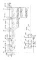
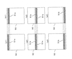
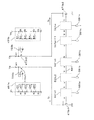
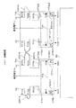
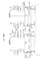
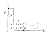
次に、本発明のEL表示パネルあるいはEL表示装置について説明をする。図6はEL表示装置の回路を中心とした説明図である。画素16がマトリックス状に配置または形成されている。各画素16には各画素の電流プログラムを行う電流を出力するソースドライバ回路14が接続されている。ソースドライバ回路14の出力段は映像信号のビット数に対応したカレントミラー回路が形成されている(後に説明する)。たとえば、64階調であれば、63個のカレントミラー回路が各ソース信号線に形成され、これらのカレントミラー回路の個数を選択することにより所望の電流をソース信号線18に印加できるように構成されている(図48を参照のこと)。
Next, the EL display panel or EL display device of the present invention will be described. FIG. 6 is an explanatory diagram focusing on the circuit of the EL display device.
なお、1つのカレントミラー回路の最小出力電流は10nA以上50nAにしている。特にカレントミラー回路の最小出力電流は15nA以上35nAにすることがよい。ドライバIC14内のカレントミラー回路を構成するトランジスタの精度を確保するためである。
The minimum output current of one current mirror circuit is 10 nA or more and 50 nA. In particular, the minimum output current of the current mirror circuit is preferably 15 nA or more and 35 nA. This is to ensure the accuracy of the transistors constituting the current mirror circuit in the
また、ソース信号線18の電荷を強制的に放出または充電するプリチャージあるいはディスチャージ回路を内蔵する。ソース信号線18の電荷を強制的に放出または充電するプリチャージあるいはディスチャージ回路の電圧(電流)出力値は、R、G、Bで独立に設定できるように構成することが好ましい。EL素子15の閾値がRGBで異なるからである(プリチャージ回路については図65、図67およびその説明を参照のこと)。
A precharge or discharge circuit for forcibly releasing or charging the
有機EL素子は大きな温度依存性特性(温特)があることが知られている。この温特による発光輝度変化を調整するため、カレントミラー回路に出力電流を変化させるサーミスタあるいはポジスタなどの非直線素子を付加し、温特による変化を前記サーミスタなどで調整することによりアナログ的に基準電流を調整する(変化させる)。 It is known that an organic EL element has a large temperature dependency characteristic (temperature characteristic). In order to adjust the light emission luminance change due to the temperature characteristics, a non-linear element such as a thermistor or a posistor that changes the output current is added to the current mirror circuit, and the temperature characteristics change is adjusted by the thermistor as an analog reference. Adjust (change) the current.
本発明において、ソースドライバ14は半導体シリコンチップで形成し、ガラスオンチップ(COG)技術で基板71のソース信号線18の端子と接続されている。ソースドライバ14の実装は、COG技術に限定するものではなく、チップオンフィルム(COF)技術に前述のソースドライバIC14などを積載し、表示パネルの信号線と接続した構成としてもよい。また、ドライブICは電源IC82を別途作製し、3チップ構成としてもよい。
In the present invention, the
一方、ゲートドライバ回路12は低温ポリシリコン技術で形成している。つまり、画素のトランジスタと同一のプロセスで形成している。これは、ソースドライバ回路14に比較して内部の構造が容易で、動作周波数も低いためである。したがって、低温ポリシリ技術で形成しても容易に形成することができ、また、狭額縁化を実現できる。もちろん、ゲートドライバ12をシリコンチップで形成し、COG技術などを用いて基板71上に実装してもよいことは言うまでもない。また、画素トランジスタなどのスイッチング素子、ゲートドライバなどは高温ポリシリコン技術で形成してもよく、有機材料で形成(有機トランジスタ)してもよい。
On the other hand, the
ゲートドライバ12はゲート信号線17a用のシフトレジスタ回路61aと、ゲート信号線17b用のシフトレジスタ回路61bとを内蔵する。各シフトレジスタ回路61は正相と負相のクロック信号(CLKxP、CLKxN)、スタートパルス(STx)で制御される(図6を参照のこと)。その他、ゲート信号線の出力、非出力を制御するイネーブル(ENABL)信号、シフト方向を上下逆転するアップダウン(UPDWM)信号を付加することが好ましい。他に、スタートパルスがシフトレジスタにシフトされ、そして出力されていることを確認する出力端子などを設けることが好ましい。なお、シフトレジスタのシフトタイミングはコントロールIC81からの制御信号で制御される。また、外部データのレベルシフトを行うレベルシフト回路を内蔵する。
The
シフトレジスタ回路61のバッファ容量は小さいため、直接にはゲート信号線17を駆動することができない。そのため、シフトレジスタ回路61の出力とゲート信号線17を駆動する出力ゲート63間には少なくとも2つ以上のインバータ回路62が形成されている。
Since the buffer capacity of the
ソースドライバ14を低温ポリシリなどのポリシリ技術で基板71上に直接形成する場合も同様であり、ソース信号線18を駆動するトランスファーゲートなどのアナログスイッチのゲートとソースドライバ回路14のシフトレジスタ間には複数のインバータ回路が形成される。以下の事項(シフトレジスタの出力と、信号線を駆動する出力段(出力ゲートあるいはトランスファーゲートなどの出力段間に配置されるインバータ回路に関する事項)は、ソースドライブおよびゲートドライブ回路に共通の事項である。
The same applies to the case where the
たとえば、図6ではソースドライバ14の出力が直接ソース信号線18に接続されているように図示したが、実際には、ソースドライバのシフトレジスタの出力は多段のインバータ回路が接続されて、インバータの出力がトランスファーゲートなどのアナログスイッチのゲートに接続されている。
For example, FIG. 6 shows that the output of the
インバータ回路62はPチャンネルのMOSトランジスタとNチャンネルのMOSトランジスタから構成される。先にも説明したようにゲートドライバ回路12のシフトレジスタ回路61の出力端にはインバータ回路62が多段に接続されており、その最終出力が出力ゲート回路63に接続されている。なお、インバータ回路62はPチャンネルのみで構成してもよい。ただし、この場合は、インバータではなく単なるゲート回路として構成してもよい。
The
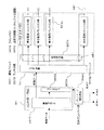
図8は本発明の表示装置の信号、電圧の供給の構成図あるいは表示装置の構成図である。コントロールIC81からソースドライバ回路14aに供給する信号(電源配線、データ配線など)はフレキシブル基板84を介して供給する。
FIG. 8 is a configuration diagram of signal and voltage supply of the display device of the present invention or a configuration diagram of the display device. Signals (power supply wiring, data wiring, etc.) supplied from the
図8ではゲートドライバ12の制御信号はコントロールICで発生させ、ソースドライバ14で、レベルシフトを行った後、ゲートドライバ12に印加している。ソースドライバ14の駆動電圧は4〜8(V)であるから、コントロールIC81から出力された3.3(V)振幅の制御信号を、ゲートドライバ12が受け取れる5(V)振幅に変換することができる。
In FIG. 8, the control signal for the
なお、図8などにおいて14をソースドライバと記載したが、単なるドライバだけでなく、電源回路、バッファ回路(シフトレジスタなどの回路を含む)、データ変換回路、ラッチ回路、コマンドデコーダ、シフト回路、アドレス変換回路、画像メモリなどを内蔵させてもよい。なお、図8などで説明する構成にあっても、図9などで説明する3辺フリー構成あるいは構成、駆動方式などを適用できることはいうまでもない。 8 is described as a source driver in FIG. 8 and the like, but not only a driver, but also a power supply circuit, a buffer circuit (including a circuit such as a shift register), a data conversion circuit, a latch circuit, a command decoder, a shift circuit, an address A conversion circuit, an image memory, or the like may be incorporated. Needless to say, the three-side free configuration or configuration described in FIG. 9 or the like, the driving method, or the like can be applied to the configuration described in FIG. 8 or the like.
コントロールIC81、電源IC82を積載した基板83は、図361に図示するように、封止基板85(封止フタ85)に形成した凹部に、部品などが挿入されるように配置する。図361のように構成することにより、パネルモジュールをコンパクトにできる。
As shown in FIG. 361, the
表示パネルを携帯電話などの情報表示装置に使用する場合、図9に示すように、ソースドライバIC(回路)14、ゲートドライバIC(回路)12は、表示パネルの一辺に実装(形成)することが好ましい(なお、このように一辺にドライバIC(回路)を実装(形成)する形態を3辺フリー構成(構造)と呼ぶ。従来は、表示領域のX辺にゲートドライバIC12が実装され、Y辺にソースドライバIC14が実装されていた)。画面50の中心線が表示装置の中心になるように設計し易く、また、ドライバICの実装も容易となるからである。なお、ゲートドライバ回路を高温ポリシリコンあるいは低温ポリシリコン技術などで3辺フリーの構成で作製してもよい(つまり、図9のソースドライバ回路14とゲートドライバ回路12のうち、少なくとも一方をポリシリコン技術で基板71に直接形成する)。
When the display panel is used for an information display device such as a mobile phone, as shown in FIG. 9, the source driver IC (circuit) 14 and the gate driver IC (circuit) 12 are mounted (formed) on one side of the display panel. (A configuration in which the driver IC (circuit) is mounted (formed) on one side in this way is called a three-side free configuration (structure). Conventionally, the
なお、3辺フリー構成とは、基板71に直接ICを積載あるいは形成した構成だけでなく、ソースドライバIC(回路)14、ゲートドライバIC(回路)12などを取り付けたフィルム(TCP、TAB技術など)を基板71の一辺(もしくはほぼ一辺)にはりつけた構成も含む。つまり、2辺にICが実装あるいは取り付けられていない構成、配置あるいはそれに類似するすべてを意味する。
The three-side free configuration is not only a configuration in which an IC is directly stacked or formed on the
図9のようにゲートドライバ回路12をソースドライバ回路14の横に配置すると、ゲート信号線17は辺Cにそって形成する必要がある。
When the
なお、図9などにおいて太い実線で図示した箇所はゲート信号線17が並列して形成した箇所を示している。したがって、bの部分(画面下部)は走査信号線の本数分のゲート信号線17が並列して形成され、aの部分(画面上部)はゲート信号線17が1本形成されている。
In FIG. 9 and the like, a portion indicated by a thick solid line indicates a portion where the
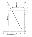
C辺に形成するゲート信号線17のピッチは5μm以上12μm以下にする。5μm未満では隣接ゲート信号線に寄生容量の影響によりノイズが乗ってしまう。実験によれば7μ以下で寄生容量の影響が顕著に発生する。さらに5μm未満では表示画面にビート状などの画像ノイズが激しく発生する。特にノイズの発生は画面の左右で異なり、このビート状などの画像ノイズを低減することは困難である。また、低減12μmを越えると表示パネルの額縁幅Dが大きくなりすぎ実用的でない。
The pitch of the
前述の画像ノイズを低減するためには、ゲート信号線17を形成した部分の下層あるいは上層に、グラントパターン(一定電圧に電圧固定あるいは全体として安定した電位に設定されている導電パターン)を配置することにより低減できる。また、別途設けたシールド板(シールド箔(一定電圧に電圧固定あるいは全体として安定した電位に設定されている導電パターン))をゲート信号線17上に配置すればよい。
In order to reduce the image noise described above, a grant pattern (a conductive pattern whose voltage is fixed to a constant voltage or set to a stable potential as a whole) is disposed in the lower layer or upper layer of the portion where the
図9のC辺のゲート信号線17はITO電極で形成してもよいが、低抵抗化するため、ITOと金属薄膜とを積層して形成することが好ましい。また、金属膜で形成することが好ましい。ITOと積層する場合は、ITO上にチタン膜を形成し、その上にアルミニウムあるいはアルミニウムとモリブデンの合金薄膜を形成する。もしくはITO上にクロム膜を形成する。金属膜の場合は、アルミニウム薄膜、クロム薄膜で形成する。以上の事項は本発明の他の実施例でも同様である。
Although the
なお、図9などにおいて、ゲート信号線17などは表示領域の片側に配置するとしたがこれに限定するものではなく、両方に配置してもよい。たとえば、ゲート信号線17aを表示領域50の右側に配置(形成)し、ゲート信号線17bを表示領域50の左側に配置(形成)してもよい。以上の事項は他の実施例でも同様である。
In FIG. 9 and the like, the
また、ソースドライバIC14とゲートドライバIC12とを1チップ化してもよい。1チップ化すれば、表示パネルへのICチップの実装が1個で済む。したがって、実装コストも低減できる。また、1チップドライバIC内で使用する各種電圧も同時に発生することができる。
Further, the
なお、ソースドライバIC14、ゲートドライバIC12はシリコンなどの半導体ウエハで作製し、表示パネルに実装するとしたがこれに限定するものではなく、低温ポリシリコン技術、高温ポリシリコン技術により表示パネル82に直接形成してもよいことは言うまでもない。
The
なお、画素は、R、G、Bの3原色としたがこれに限定するものではなく、シアン、イエロー、マゼンダの3色でもよい。また、Bとイエローの2色でもよい。もちろん、単色でもよい。また、R、G、B、シアン、イエロー、マゼンダの6色でもよい。R、G、B、シアン、マゼンダの5色でもよい。これらはナチュラルカラーとして色再現範囲が拡大し良好な表示を実現できる。以上のように本発明のEL表示装置は、RGBの3原色でカラー表示を行うものに限定されるものではない。 The pixels are R, G, and B primary colors. However, the present invention is not limited to this, and may be cyan, yellow, and magenta. Also, two colors of B and yellow may be used. Of course, it may be a single color. Also, six colors of R, G, B, cyan, yellow, and magenta may be used. Five colors of R, G, B, cyan, and magenta may be used. These are natural colors, and the color reproduction range is expanded to achieve a good display. As described above, the EL display device of the present invention is not limited to one that performs color display with the three primary colors RGB.
有機EL表示パネルのカラー化には主に三つの方式があり、色変換方式はこのうちの一つである。発光層として青色のみの単層を形成すればよく、フルカラー化に必要な残りの緑色と赤色は、青色光から色変換によって作り出す。したがって、RGBの各層を塗り分ける必要がない、RGBの各色の有機EL材料をそろえる必要がないという利点がある。色変換方式は、塗り分け方式のようは歩留まり低下がない。本発明のEL表示パネルなどはこのいずれの方式でも適用される。 There are mainly three methods for colorizing an organic EL display panel, and one of them is a color conversion method. It is only necessary to form a blue-only single layer as the light emitting layer, and the remaining green and red colors necessary for full color are generated from blue light by color conversion. Therefore, there is an advantage that it is not necessary to separately coat each layer of RGB, and it is not necessary to prepare organic EL materials of each color of RGB. The color conversion method does not cause a decrease in yield unlike the color separation method. The EL display panel of the present invention can be applied to any of these methods.
また、3原色の他に、白色発光の画素を形成してもよい。白色発光の画素はR、G、B発光の構造を積層することのより作製(形成または構成)することにより実現できる。1組の画素は、RGBの3原色と、白色発光の画素16Wからなる。白色発光の画素を形成することにより、白色のピーク輝度が表現しやすくなる。したがって、輝き感のある画像表示実現できる。
In addition to the three primary colors, white light emitting pixels may be formed. A white light emitting pixel can be realized by forming (forming or configuring) by stacking R, G, and B light emitting structures. One set of pixels includes three primary colors of RGB and a
RGBなどの3原色を1組の画素をする場合であっても、各色の画素電極の面積は異ならせることが好ましい。もちろん、各色の発光効率がバランスよく、色純度もバランスがよければ、同一面積でもかまわない。しかし、1つまたは複数の色のバランスが悪ければ、画素電極(発光面積)を調整することが好ましい。各色の電極面積は電流密度を基準に決定すればよい。つまり、色温度が7000K(ケルビン)以上12000K以下の範囲で、ホワイトバランスを調整した時、各色の電流密度の差が±30%以内となるようにする。さらに好ましくは±15%以内となるようにする。たとえば、電流密度が100A/平方メーターをすれば、3原色がいずれも70A/平方メーター以上130A/平方メーター以下となるようにする。さらに好ましくは、3原色がいずれも85A/平方メーター以上115A/平方メーター以下となるようにする。 Even in the case of forming a set of pixels for three primary colors such as RGB, it is preferable that the areas of the pixel electrodes of the respective colors are different. Of course, if the luminous efficiency of each color is well balanced and the color purity is well balanced, the same area may be used. However, if the balance of one or more colors is bad, it is preferable to adjust the pixel electrode (light emitting area). The electrode area of each color may be determined based on the current density. That is, when the white balance is adjusted within a color temperature range of 7000 K (Kelvin) to 12000 K, the difference in current density of each color is within ± 30%. More preferably, it is within ± 15%. For example, if the current density is 100 A / square meter, the three primary colors are all set to 70 A / square meter or more and 130 A / square meter or less. More preferably, the three primary colors are all set to 85 A / square meter or more and 115 A / square meter or less.
有機EL素子15は自己発光素子である。この発光による光がスイッチング素子としてのトランジスタに入射するとホトコンダクタ現象(ホトコン)が発生する。ホトコンとは、光励起によりトランジスタなどのスイッチング素子のオフ時でのリーク(オフリーク)が増える現象を言う。
The
この課題に対処するため、本発明ではゲートドライバ12(場合によってはソースドライバ14)の下層、画素トランジスタ11の下層の遮光膜を形成している。遮光膜はクロムなどの金属薄膜で形成し、その膜厚は50nm以上150nm以下にする。膜厚が薄いと遮光効果が乏しく、厚いと凹凸が発生して上層のトランジスタ11A1のパターニングが困難になる。
In order to cope with this problem, in the present invention, a light shielding film under the gate driver 12 (in some cases, the source driver 14) and under the
ドライバ回路12などは裏面だけでなく、表面からの光の進入も抑制するべきである。ホトコンの影響により誤動作するからである。したがって、本発明では、カソード電極が金属膜の場合は、ドライバ12などの表面にもカソード電極を形成し、この電極を遮光膜として用いている。
The
しかし、ドライバ12の上にカソード電極を形成すると、このカソード電極からの電界によるドライバの誤動作あるいはカソード電極とドライバ回路の電気的接触が発生する可能性がある。この課題に対処するため、本発明ではドライバ回路12などの上に少なくとも1層、好ましくは複数層の有機EL膜を画素電極上の有機EL膜形成と同時に形成する。
However, when a cathode electrode is formed on the
画素の1つ以上のトランジスタ11の端子間あるいはトランジスタ11と信号線とが短絡すると、EL素子15が常時、点灯する輝点となる場合がある。この輝点は視覚的にめだつので黒点化(非点灯)する必要がある。輝点に対しては、該当画素16を検出し、コンデンサ19にレーザー光を照射してコンデンサの端子間を短絡させる。したがって、コンデンサ19には電荷を保持できなくなるので、トランジスタ11aは電流を流さなくすることができる。レーザー光を照射する位置にあたるカソード膜を除去しておくことが望ましい。レーザー照射により、コンデンサ19の端子電極とカソード膜とがショートすることを防止するためである。
When the terminals of one or
画素16のトランジスタ11の欠陥は、ドライバIC14などにも影響を与える。例えば、図45では駆動用トランジスタ11aにソース−ドレイン(SD)ショート452が発生していると、パネルのVdd電圧がソースドライバIC14に印加される。したがって、ソースドライバIC14の電源電圧は、パネルの電源電圧Vddと同一かもしくは高くしておくことが好ましい。なお、ソースドライバICで使用する基準電流は電子ボリウム451で調整できるように構成しておくことが好ましい。
The defect of the
トランジスタ11aにSDショート452が発生していると、EL素子15に過大な電流が流れる。つまり、EL素子15が常時点灯状態(輝点)となる。輝点は欠陥として目立ちやすい。たとえば、図45において、トランジスタ11aのソース−ドレイン(SD)ショートが発生していると、トランジスタ11aのゲート(G)端子電位の大小に関わらず、Vdd電圧からEL素子15に電流が常時流れる(トランジスタ11dがオンの時)。したがって、輝点となる。
When the SD short 452 is generated in the
一方、トランジスタ11aにSDショートが発生していると、トランジスタ11cがオン状態の時、Vdd電圧がソース信号線18に印加されソースドライバ14にVdd電圧が印加される。もし、ソースドライバ14の電源電圧がVdd以下であれば、耐圧を越えて、ソースドライバ14が破壊される恐れがある。そのため、ソースドライバ14の電源電圧はVdd電圧(パネルの高い方の電圧)以上にすることが好ましい。
On the other hand, when an SD short occurs in the
トランジスタ11aのSDショートなどは、点欠陥にとどまらず、パネルのソースドライバ回路を破壊につながる恐れがあり、また、輝点は目立つためパネルとしては不良となる。したがって、トランジスタ11aとEL素子15間を接続する配線を切断し、輝点を黒点欠陥にする必要がある。この切断には、レーザー光などの光学手段を用いて切断することがよい。
The SD short of the
以下、本発明の駆動方法について説明をする。図1に示すように、ゲート信号線17aは行選択期間に導通状態(ここでは図1のトランジスタ11がpチャネルトランジスタであるためローレベルで導通となる)となり、ゲート信号線17bは非選択期間時に導通状態とする。
Hereinafter, the driving method of the present invention will be described. As shown in FIG. 1, the
ソース信号線18には寄生容量(図示せず)が存在する。寄生容量は、ソース信号線18とゲート信号線17とのクロス部の容量、トランジスタ11b、11cのチャンネル容量などにより発生する。
The
なお、寄生容量は、ソース信号線18だけでなく、ソースドライバIC14でも発生する。図273に図示するように、保護ダイオード2731が主原因である。保護ダイオード2731は、IC14を静電気保護する目的を有するが、コンデンサともなってしまう。一般的な保護ダイオードの容量は3〜5pFである。
Parasitic capacitance is generated not only in the
本発明のソースドライバIC(後に詳細に説明をする)では、図273に図示するように、端子681と出力段654間にサージ低減抵抗2732を形成または配置している。抵抗2732はポリシリコンまたは拡散抵抗で形成する。抵抗値は、1KΩ以上1MΩ以下とする。この抵抗により、外部からの静電気が抑制される。したがって、保護ダイオード2731のサイズが小さくともよい。保護ダイオード2731が小さければ保護ダイオードのよる寄生容量の大きさも小さくなる。なお、図273ではソースドライバIC14内に抵抗2732を形成または配置しているように図示しているがこれに限定するものではなく、抵抗2732は、アレイ71に形成または配置してもよいことはいうまでもない。また、ダイオード(トランジスタをダイオード構成にしたものを含む)2731についても同様である。
In the source driver IC of the present invention (which will be described in detail later), a
ソース信号線18の電流値変化に要する時間tは浮遊容量の大きさをC、ソース信号線の電圧をV、ソース信号線に流れる電流をIとするとt=C・V/Iであるため電流値を10倍大きくできることは電流値変化に要する時間が10分の1近くまで短くできる。または、ソース信号線18の寄生容量が10倍になっても所定の電流値に変化できるということを示す。従って、短い水平走査期間内に所定の電流値を書きこむためには電流値を増加させることが有効である。
The time t required to change the current value of the
入力電流を10倍にすると出力電流も10倍となり、ELの輝度が10倍となるため所定の輝度を得るために、図1のトランジスタ17dの導通期間を従来の10分の1とし、発光期間を10分の1とすることで、所定輝度を表示するようにした。なお、10倍を例示して説明しているのは理解を容易にするためである。10倍に限定するものでないことは言うまでもない。 When the input current is increased 10 times, the output current is also increased 10 times, and the luminance of EL is increased 10 times. Therefore, in order to obtain a predetermined luminance, the conduction period of the transistor 17d in FIG. By setting the value to 1/10, a predetermined luminance is displayed. Note that the explanation is given by exemplifying 10 times for easy understanding. Needless to say, it is not limited to 10 times.
つまり、ソース信号線18の寄生容量の充放電を十分に行い、所定の電流値を画素16のトランジスタ11aにプログラムを行うためには、ソースドライバ14から比較的大きな電流を出力する必要がある。しかし、このように大きな電流をソース信号線18に流すとこの電流値が画素にプログラムされてしまい、所定の電流に対し大きな電流がEL素子15に流れる。たとえば、10倍の電流でプログラムすれば、当然、10倍の電流がEL素子15に流れ、EL素子15は10倍の輝度で発光する。所定の発光輝度にするためには、EL素子15に流れる時間を1/10にすればよい。このように駆動することにより、ソース信号線18の寄生容量を十分に充放電できるし、所定の発光輝度を得ることができる。
That is, it is necessary to output a relatively large current from the
なお、10倍の電流値を画素のトランジスタ11a(正確にはコンデンサ19の端子電圧を設定している)に書き込み、EL素子15のオン時間を1/10にするとしたがこれは一例である。場合によっては、10倍の電流値を画素のトランジスタ11aに書き込み、EL素子15のオン時間を1/5にしてもよい。逆に10倍の電流値を画素のトランジスタ11aに書き込み、EL素子15のオン時間を1/2倍にする場合もあるであろう。
It should be noted that although 10 times the current value is written in the
本発明は、画素への書き込み電流を所定値以外の値にし、EL素子15に流れる電流を間欠状態にして駆動することに特徴がある。本明細書では説明を容易にするため、N倍の電流値を画素のトランジスタ11に書き込み、EL素子15のオン時間を1/N倍にするとして説明する。しかし、これに限定するものではなく、N1倍の電流値を画素のトランジスタ11に書き込み、EL素子15のオン時間を1/(N2)倍(N1とN2とは異なる)でもよいことは言うまでもない。
The present invention is characterized in that the pixel write current is set to a value other than a predetermined value and the current flowing through the
白ラスター表示において、表示画面50の1フィールド(フレーム)期間の平均輝度をB0と仮定する。この時、各画素16の輝度B1が平均輝度B0よりも高くなるように電流(電圧)プログラムを行う駆動方法である。かつ、少なくとも1フィールド(フレーム)期間において、非表示領域53が発生するようにする駆動方法である。したがって、本発明の駆動方法では、1フィールド(フレーム)期間の平均輝度はB1よりも低くなる。
In the white raster display, it is assumed that the average luminance in one field (frame) period of the
なお、間欠する間隔(非表示領域52/表示領域53)は等間隔に限定するものではない。たとえば、ランダムでもよい(全体として、表示期間もしくは非表示期間が所定値(一定割合)となればよい)。また、RGBで異なっていてもよい。つまり、白(ホワイト)バランスが最適になるように、R、G、B表示期間もしくは非表示期間が所定値(一定割合)となるように調整(設定)すればよい。
The intermittent interval (
本発明の駆動方法の説明を容易にするため、1/Nとは、1F(1フィールドまたは1フレーム)を基準にしてこの1Fを1/Nにするとして説明する。しかし、1画素行が選択され、電流値がプログラムされる時間(通常、1水平走査期間(1H))があるし、また、走査状態によっては誤差も生じることは言うまでもない。 In order to facilitate the description of the driving method of the present invention, 1 / N is described on the assumption that 1F is set to 1 / N on the basis of 1F (one field or one frame). However, there is a time during which one pixel row is selected and the current value is programmed (usually, one horizontal scanning period (1H)), and it goes without saying that an error may occur depending on the scanning state.
たとえば、N=10倍の電流で画素16に電流プログラムし、1/5の期間の間、EL素子15を点灯させてもよい。EL素子15は、10/5=2倍の輝度で点灯する。N=2倍の電流で画素16に電流プログラムし、1/4の期間の間、EL素子15を点灯させてもよい。EL素子15は、2/4=0.5倍の輝度で点灯する。つまり、本発明は、N=1倍でない電流でプログラムし、かつ、常時点灯(1/1、つまり、間欠表示でない)状態以外の表示を実施するものである。また、EL素子15に供給する電流を1フレーム(あるいは1フィールド)の期間において、少なくとも1回、オフする駆動方式である。また、所定値よりも大きな電流で画素16にプログラムし、少なくとも、間欠表示を実施する駆動方式である。
For example, the
有機(無機)EL表示装置は、CRTのように電子銃で線表示の集合として画像を表示するディスプレイとは表示方法が基本的に異なる点にも課題がある。つまり、EL表示装置では、1F(1フィールドあるいは1フレーム)の期間の間は、画素に書き込んだ電流(電圧)を保持する。そのため、動画表示を行うと表示画像の輪郭ぼけが発生するという課題が発生する。 The organic (inorganic) EL display device also has a problem in that the display method is basically different from a display that displays an image as a set of line displays with an electron gun, such as a CRT. That is, in the EL display device, the current (voltage) written to the pixel is held for a period of 1F (1 field or 1 frame). For this reason, when a moving image is displayed, there is a problem that the outline of the display image is blurred.
本発明では、1F/Nの期間の間だけ、EL素子15に電流を流し、他の期間(1F(N−1)/N)は電流を流さない。この駆動方式を実施し画面の一点を観測した場合を考える。この表示状態では1Fごとに画像データ表示、黒表示(非点灯)が繰り返し表示される。つまり、画像データ表示状態が時間的に間欠表示状態となる。動画データ表示を、間欠表示状態でみると画像の輪郭ぼけがなくなり良好な表示状態を実現できる。つまり、CRTに近い動画表示を実現することができる。
In the present invention, a current is passed through the
本発明の駆動方法では、間欠表示を実現する。しかし、間欠表示は、トランジスタ11dを1H周期でオンオフ制御するだけでよい。したがって、回路のメインクロックは従来と変わらないため、回路の消費電力が増加することもない。液晶表示パネルでは、間欠表示を実現するために画像メモリが必要である。本発明は、画像データは各画素16に保持されている。したがって、間欠表示を実施するための画像メモリは不要である。
In the driving method of the present invention, intermittent display is realized. However, the intermittent display only needs to be turned on / off for the
本発明はスイッチングのトランジスタ11d、あるいはトランジスタ11eなどをオンオフさせるだけでEL素子15に流す電流を制御する。つまり、EL素子15に流れる電流Iwをオフしても、画像データはそのままコンデンサ19の保持されている。したがって、次のタイミングでスイッチング素子11dなどをオンさせ、EL素子15に電流を流せば、その流れる電流は前に流れていた電流値と同一である。本発明では黒挿入(黒表示などの間欠表示)を実現する際においても、回路のメインクロックをあげる必要がない。また、時間軸伸張を実施する必要もないための画像メモリも不要である。また、有機EL素子15は電流を印加してから発光するまでの時間が短く、高速に応答する。そのため、動画表示に適し、さらに間欠表示を実施することのより従来のデータ保持型の表示パネル(液晶表示パネル、EL表示パネルなど)の問題である動画表示の問題を解決できる。
In the present invention, the current supplied to the
さらに、大型の表示装置でソース信号線18の配線長が長くなり、ソース信号線18の寄生容量が大きくなる場合は、N値を大きくすることのより対応できる。ソース信号線18に印加するプログラム電流値をN倍にした場合、ゲート信号線17b(トランジスタ11d)の導通期間を1F/Nとすればよい。これによりテレビ、モニターなどの大型表示装置などにも適用が可能である。
Further, when the wiring length of the
以下、図面を参照しながら、本発明の駆動方法についてさらに詳しく説明をする。ソース信号線18の寄生容量は、隣接したソース信号線18間の結合容量、ソースドライブIC(回路)14のバッファ出力容量、ゲート信号線17とソース信号線18とのクロス容量などにより発生する。この寄生容量は通常10pF以上となる。電圧駆動の場合は、ドライバIC14からは低インピーダンスで電圧がソース信号線18に印加されるため、寄生容量が多少大きくとも駆動では問題とならない。
Hereinafter, the driving method of the present invention will be described in more detail with reference to the drawings. The parasitic capacitance of the
しかし、電流駆動では特に黒レベルの画像表示では20nA以下の微小電流で画素のコンデンサ19をプログラムする必要がある。したがって、寄生容量が所定値以上の大きさで発生すると、1画素行にプログラムする時間(通常、1H以内、ただし、2画素行を同時に書き込む場合もあるので1H以内に限定されるものではない。)内に寄生容量を充放電することができない。1H期間で充放電できなれば、画素への書き込み不足となり、解像度がでない。
However, current driving requires that the
図1の画素構成の場合、図3(a)に示すように、電流プログラム時は、プログラム電流Iwがソース信号線18に流れる。この電流Iwがトランジスタ11aを流れ、Iwを流す電流が保持されるように、コンデンサ19に電圧設定(プログラム)される。このとき、トランジスタ11dはオープン状態(オフ状態)である。
In the case of the pixel configuration of FIG. 1, as shown in FIG. 3A, the program current Iw flows through the
次に、EL素子15に電流を流す期間は図3(b)のように、トランジスタ11c、11bがオフし、トランジスタ11dが動作する。つまり、ゲート信号線17aにオフ電圧(Vgh)が印加され、トランジスタ11b、11cがオフする。一方、ゲート信号線17bにオン電圧(Vgl)が印加され、トランジスタ11dがオンする。
Next, during a period in which a current flows through the
今、電流I1が本来流す電流(所定値)のN倍であるとすると、図3(b)のEL素子15に流れる電流もIwとなる。したがって、所定値の10倍の輝度でEL素子15は発光する。つまり、図12に図示するように、倍率Nを高くするほど、画素16の表示輝度Bも高くなる。したがって、倍率と画素16の輝度とは比例関係となる。
Assuming that the current I1 is N times the current (predetermined value) that flows originally, the current flowing through the
そこで、トランジスタ11dを本来オンする時間(約1F)の1/Nの期間だけオンさせ、他の期間(N−1)/N期間はオフさせれば、1F全体の平均輝度は所定の輝度となる。この表示状態は、CRTが電子銃で画面を走査しているのと近似する。異なる点は、画像を表示している範囲が画面全体の1/N(全画面を1とする)が点灯している点である(CRTでは、点灯している範囲は1画素行(厳密には1画素である)。
Therefore, if the
本発明では、この1F/Nの画像表示領域53が図13(b)に示すように画面50の上から下に移動する。本発明では、1F/Nの期間の間だけ、EL素子15に電流が流れ、他の期間(1F・(N−1)/N)は電流が流れない。したがって、各画素16は間欠表示となる。しかし、人間の目には残像により画像が保持された状態となるので、全画面が均一に表示されているように見える。
In the present invention, the 1F / N
なお、図13に図示するように、書き込み画素行51aは非点灯表示52aとする。しかし、これは、図1、図2などの画素構成の場合である。図38などで図示するカレントミラーの画素構成では、書き込み画素行51aは点灯状態としてもよい。しかし、本明細書では、説明を容易にするため、主として、図1の画素構成を例示して説明をする。また、図13、図16などの所定駆動電流Iwよりも大きい電流でプログラムし、間欠駆動する駆動方法をN倍パルス駆動と呼ぶ。
As shown in FIG. 13, the
この表示状態では1Fごとに画像データ表示、黒表示(非点灯)が繰り返し表示される。つまり、画像データ表示状態が時間的に飛び飛び表示(間欠表示)状態となる。液晶表示パネル(本発明以外のEL表示パネル)では、1Fの期間、画素にデータが保持されているため、動画表示の場合は画像データが変化してもその変化に追従することができず、動画ボケとなっていた(画像の輪郭ボケ)。しかし、本発明では画像を間欠表示するため、画像の輪郭ぼけがなくなり良好な表示状態を実現できる。つまり、CRTに近い動画表示を実現することができる。 In this display state, image data display and black display (non-lighting) are repeatedly displayed every 1F. That is, the image data display state is a temporal display (intermittent display) state. In a liquid crystal display panel (an EL display panel other than the present invention), since data is held in pixels for a period of 1F, even if image data changes in the case of moving image display, the change cannot be followed. The video was blurred (outline blur in the image). However, since the image is intermittently displayed in the present invention, the outline of the image is not blurred and a good display state can be realized. That is, a moving image display close to a CRT can be realized.
なお、図13に図示するように、駆動するためには、画素16の電流プログラム期間(図1の画素構成においては、ゲート信号線17aのオン電圧Vglが印加されている期間)と、EL素子15をオフまたはオン制御している期間(図1の画素構成においては、ゲート信号線17bのオン電圧Vglまたはオフ電圧Vghが印加されている期間)とを独立に制御できる必要がある。したがって、ゲート信号線17aとゲート信号線17bは分離されている必要がある。
As shown in FIG. 13, in order to drive, the current program period of the pixel 16 (in the pixel configuration of FIG. 1, the period during which the ON voltage Vgl of the
たとえば、ゲートドライバ回路12から画素16に配線されたゲート信号線17が1本である場合、ゲート信号線17に印加されたロジック(VghまたはVgl)をトランジスタ11bに印加し、ゲート信号線17に印加されたロジックをインバータで変換して(VglまたはVgh)して、トランジスタ11dに印加するという構成では、本発明の駆動方法は実施できない。したがって、本発明では、ゲート信号線17aを操作するゲートドライバ回路12aと、ゲート信号線17bを操作するゲートドライバ回路12bが必要となる。
For example, when there is one
また、本発明の駆動方法は、図1の画素構成においても、電流プログラム期間(1H)以外の期間においても、非点灯表示にする駆動方法である。 In addition, the driving method of the present invention is a driving method for non-lighting display in the pixel configuration of FIG. 1 and in a period other than the current program period (1H).
図13の駆動方法のタイミングチャートを図14に図示する。なお、本発明などにおいて、特に断りがない時の画素構成は図1であるとする。図14でわかるように、各選択された画素行(選択期間は、1Hとしている)において、ゲート信号線17aにオン電圧(Vgl)が印加されている時(図14(a)を参照)には、ゲート信号線17bにはオフ電圧(Vgh)が印加されている(図14(b)を参照)。また、この期間は、EL素子15には電流が流れていない(非点灯状態)。選択されていない画素行において、ゲート信号線17aにオフ電圧(Vgh)が印加され、ゲート信号線17bにはオン電圧(Vgl)が印加されている。また、この期間は、EL素子15に電流が流れている(点灯状態)。また、点灯状態では、EL素子15は所定のN倍の輝度(N・B)で点灯し、その点灯期間は1F/Nである。したがって、1Fを平均した表示パネルの表示輝度は、(N・B)×(1/N)=B(所定輝度)となる。
FIG. 14 shows a timing chart of the driving method of FIG. In the present invention and the like, the pixel configuration when there is no particular notice is assumed to be FIG. As can be seen from FIG. 14, when an on-voltage (Vgl) is applied to the
図15は、図14の動作を各画素行に適用した実施例である。ゲート信号線17に印加する電圧波形を示している。電圧波形はオフ電圧をVgh(Hレベル)とし、オン電圧をVgl(Lレベル)としている。(1)(2)などの添え字は選択している画素行番号を示している。
FIG. 15 shows an embodiment in which the operation of FIG. 14 is applied to each pixel row. A voltage waveform applied to the
図15において、ゲート信号線17a(1)が選択され(Vgl電圧)、選択された画素行のトランジスタ11aからソースドライバ14に向かってソース信号線18にプログラム電流が流れる。このプログラム電流は所定値のN倍(説明を容易にするため、N=10として説明する。もちろん、所定値とは画像を表示するデータ電流であるから、白ラスター表示などでない限り固定値ではない。)である。したがって、コンデンサ19には10倍に電流がトランジスタ11aに流れるようにプログラムされる。画素行(1)が選択されている時は、図1の画素構成ではゲート信号線17b(1)はオフ電圧(Vgh)が印加され、EL素子15には電流が流れない。
In FIG. 15, the
1H後には、ゲート信号線17a(2)が選択され(Vgl電圧)、選択された画素行のトランジスタ11aからソースドライバ14に向かってソース信号線18にプログラム電流が流れる。このプログラム電流は所定値のN倍(説明を容易にするため、N=10として説明する)である。したがって、コンデンサ19には10倍に電流がトランジスタ11aに流れるようにプログラムされる。画素行(2)が選択されている時は、図1の画素構成ではゲート信号線17b(2)はオフ電圧(Vgh)が印加され、EL素子15には電流が流れない。しかし、先の画素行(1)のゲート信号線17a(1)にはオフ電圧(Vgh)が印加され、ゲート信号線17b(1)にはオン電圧(Vgl)が印加されるため、点灯状態となっている。
After 1H, the
次の1H後には、ゲート信号線17a(3)が選択され、ゲート信号線17b(3)はオフ電圧(Vgh)が印加され、画素行(3)のEL素子15には電流が流れない。しかし、先の画素行(1)(2)のゲート信号線17a(1)(2)にはオフ電圧(Vgh)が印加され、ゲート信号線17b(1)(2)にはオン電圧(Vgl)が印加されるため、点灯状態となっている。
After the next 1H, the
以上の動作を1Hの同期信号に同期して画像を表示していく。しかし、図15の駆動方式では、EL素子15には10倍の電流が流れる。したがって、表示画面50は約10倍の輝度で表示される。もちろん、この状態で所定の輝度表示を行うためには、プログラム電流を1/10にしておけばよいことは言うまでもない。しかし、1/10の電流であれば寄生容量などにより書き込み不足が発生するため、高い電流でプログラムし、黒画面52の挿入により所定の輝度を得るのは本発明の基本的な主旨である。
The above operation is displayed in synchronization with the 1H synchronization signal. However, in the driving method of FIG. 15, 10 times of current flows through the
なお、本発明の駆動方法において、所定電流よりも高い電流がEL素子15に流れるようにし、ソース信号線18の寄生容量を十分に充放電するという概念である。つまり、EL素子15にN倍の電流を流さなくともよい。たとえば、EL素子15に並列に電流経路を形成し(ダミーのEL素子を形成し、このEL素子は遮光膜を形成して発光させないなど)、ダミーEL素子とEL素子15に分流して電流を流しても良い。たとえば、信号電流が0.2μAのとき、プログラム電流を2.2μAとして、トランジスタ11aには2.2μAを流す。この電流のうち、信号電流0.2μAをEL素子15に流して、2μAをダミーのEL素子に流すなどの方式が例示される。つまり、図27のダミー画素行271を常時選択状態にする。なお、ダミー画素行は発光させないか、もしくは、遮光膜などを形成し、発光していても視覚的に見えないように構成する。
In the driving method of the present invention, the concept is that a current higher than a predetermined current flows in the
以上のように構成することにより、ソース信号線18に流す電流をN倍に増加させることにより、駆動用トランジスタ11aにN倍の電流が流れるようにプログラムすることができ、かつ、電流EL素子15には、N倍よりは十分小さい電流をながることができることになる。以上の方法では、図5に図示するように、非点灯領域52を設けることなく、全表示領域50を画像表示領域53とすることができる。
With the above configuration, by increasing the current flowing through the
図13(a)は表示画像50への書き込み状態を図示している。図13(a)において、51aは書き込み画素行である。ソースドライバIC14から各ソース信号線18にプログラム電流が供給される。なお、図13などでは1H期間に書き込む画素行は1行である。しかし、何ら1Hに限定するものではなく、0.5H期間でも、2H期間でもよい。また、ソース信号線18にプログラム電流を書き込むとしたが、本発明は電流プログラム方式に限定するものではなく、ソース信号線18に書き込まれるのは電圧である電圧プログラム方式(図46など)でもよい。
FIG. 13A illustrates a writing state on the
図13(a)において、ゲート信号線17aが選択されるとソース信号線18に流れる電流がトランジスタ11aにプログラムされる。この時、ゲート信号線17bはオフ電圧が印加されEL素子15には電流が流れない。これは、EL素子15側にトランジスタ11dがオン状態であると、ソース信号線18からEL素子15の容量成分が見え、この容量に影響されてコンデンサ19に十分に正確な電流プログラムができなくなるためである。したがって、図1の構成を例にすれば、図13(b)で示すように電流を書き込まれている画素行は非点灯領域52となる。
In FIG. 13A, when the
今、N(ここでは、先に述べたようにN=10とする)倍の電流でプログラムしたとすれば、画面の輝度は10倍になる。したがって、表示領域50の90%の範囲を非点灯領域52とすればよい。したがって、画像表示領域の水平走査線がQCIFの220本(S=220)とすれば、22本と表示領域53とし、220−22=198本を非表示領域52とすればよい。一般的に述べれば、水平走査線(画素行数)をSとすれば、S/Nの領域を表示領域53とし、この表示領域53をN倍の輝度で発光させる。そして、この表示領域53を画面の上下方向に走査する。したがって、S(N−1)/Nの領域は非点灯領域52とする。この非点灯領域は黒表示(非発光)である。また、この非発光部52はトランジスタ11dをオフさせることにより実現する。なお、N倍の輝度で点灯させるとしたが、当然のことながら明るさ調整、ガンマ調整によりN倍の値と調整することは言うまでもない。
Now, if the current is programmed with N times (N = 10 as described above), the screen brightness will be 10 times. Therefore, a 90% range of the
また、先の実施例で、10倍の電流でプログラムしたとすれば、画面の輝度は10倍になり、表示領域50の90%の範囲を非点灯領域52とすればよいとした。しかし、これは、RGBの画素を共通に非点灯領域52とすることに限定するものではない。例えば、Rの画素は、1/8を非点灯領域52とし、Gの画素は、1/6を非点灯領域52とし、Bの画素は、1/10を非点灯領域52と、それぞれの色により変化させてもよい。また、RGBの色で個別に非点灯領域52(あるいは点灯領域53)を調整できるようにしてもよい。これらを実現するためには、R、G、Bで個別のゲート信号線17bが必要になる。しかし、以上のRGBの個別調整を可能にすることにより、ホワイトバランスを調整することが可能になり、各階調において色のバランス調整が容易になる(図41を参照のこと)。
Further, in the previous embodiment, if programming was performed with 10 times the current, the brightness of the screen would be 10 times, and 90% of the
図13(b)に図示するように、書き込み画素行51aを含む画素行が非点灯領域52とし、書き込み画素行51aよりも上画面のS/N(時間的には1F/N)の範囲を表示領域53とする(書き込み走査が画面の上から下方向の場合、画面を下から上に走査する場合は、その逆となる)。画像表示状態は、表示領域53が帯状になって、画面の上から下に移動する。
As shown in FIG. 13B, the pixel row including the
図13の表示では、1つの表示領域53が画面の上から下方向に移動する。フレームレートが低いと、表示領域53が移動するのが視覚的に認識される。特に、まぶたを閉じた時、あるいは顔を上下に移動させた時などに認識されやすくなる。
In the display of FIG. 13, one
この課題に対しては、図16に図示するように、表示領域53を複数に分割するとよい。この分割された総和がS(N−1)/Nの面積となれば、図13の明るさと同等になる。なお、分割された表示領域53は等しく(等分に)する必要はない。また、分割された非表示領域52も等しくする必要はない。
For this problem, the
以上のように、表示領域53を複数に分割することにより画面のちらつきは減少する。したがって、フリッカの発生はなく、良好な画像表示を実現できる。なお、分割はもっと細かくしてもよい。しかし、分割するほど動画表示性能は低下する。
As described above, screen flickering is reduced by dividing
図17はゲート信号線17の電圧波形およびELの発光輝度を図示している。図17で明らかなように、ゲート信号線17bをVglにする期間(1F/N)を複数に分割(分割数K)している。つまり、Vglにする期間は1F/(K・N)の期間をK回実施する。このように制御すれば、フリッカの発生を抑制でき、低フレームレートの画像表示を実現できる。また、この画像の分割数も可変できるように構成することが好ましい。たとえば、ユーザーが明るさ調整スイッチを押すことにより、あるいは明るさ調整ボリウムを回すことにより、この変化を検出してKの値を変更してもよい。また、ユーザーが輝度を調整するように構成してもよい。表示する画像の内容、データにより手動で、あるいは自動的に変化させるように構成してもよい。
FIG. 17 shows the voltage waveform of the
なお、図17などにおいて、ゲート信号線17bをVglにする期間(1F/N)を複数に分割(分割数K)し、Vglにする期間は1F/(K・N)の期間をK回実施するとしたがこれ限定するものではない。1F/(K・N)の期間をL(L≠K)回実施してもよい。つまり、本発明は、EL素子15に流す期間(時間)を制御することにより画像50を表示するものである。したがって、1F/(K・N)の期間をL(L≠K)回実施することは本発明の技術的思想に含まれる。また、Lの値を変化させることにより、画像50の輝度をデジタル的に変更することができる。たとえば、L=2とL=3では50%の輝度(コントラスト)変化となる。また、画像の表示領域53を分割する時、ゲート信号線17bをVglにする期間は同一期間に限定するものではない。
In FIG. 17 and the like, the period (1F / N) for setting the
以上の実施例は、EL素子15に流れる電流を遮断し、また、EL素子に流れる電流を接続することにより、表示画面50をオンオフ(点灯、非点灯)するものであった。つまり、コンデンサ19に保持された電荷によりトランジスタ11aに複数回、略同一電流を流すものである。本発明はこれに限定するものではない。たとえば、コンデンサ19に保持された電荷を充放電させることにより、表示画面50をオンオフ(点灯、非点灯)する方式でもよい。
In the above embodiment, the current flowing through the
図18は図16の画像表示状態を実現するための、ゲート信号線17に印加する電圧波形である。図18と図15の差異は、ゲート信号線17bの動作である。ゲート信号線17bは画面を分割する個数に対応して、その個数分だけオンオフ(VglとVgh)動作する。他の点は図15と同一であるので説明を省略する。
FIG. 18 shows voltage waveforms applied to the
EL表示装置では黒表示は完全に非点灯であるから、液晶表示パネルを間欠表示した場合のように、コントラスト低下もない。また、図1、図2、図32、図43、図117の構成においては、トランジスタ11dをオンオフ操作するだけで間欠表示を実現できる。また、図38、図51、図115の構成においては、トランジスタ素子11eをオンオフ操作するだけで、間欠表示を実現することができる。また、図113においては切り替え回路1131を制御することにより間欠表示を実現できる。また、図114においては、トランジスタ11gをオンオフ制御することにより間欠表示を実現できる。これは、コンデンサ19に画像データがメモリ(アナログ値であるから階調数は無限大)されているからである。つまり、各画素16に、画像データは1Fの期間中は保持されている。この保持されている画像データに相当する電流をEL素子15に流すか否かをトランジスタ11d、11eの制御により実現しているのである。
In the EL display device, since the black display is completely unlit, there is no reduction in contrast as in the case where the liquid crystal display panel is intermittently displayed. In the configurations of FIGS. 1, 2, 32, 43, and 117, intermittent display can be realized only by turning on and off the
したがって、以上の駆動方法は、電流駆動方式に限定されるものではなく、電圧駆動方式にも適用できるものである。つまり、EL素子15に流す電流が各画素内で保存している構成において、駆動用トランジスタ11をEL素子15間の電流経路をオンオフすることにより、間欠駆動を実現するものである。
Therefore, the above driving method is not limited to the current driving method, but can also be applied to the voltage driving method. That is, in the configuration in which the current flowing through the
コンデンサ19の端子電圧を維持することはフリッカ低減と低消費電力化に重要である。1フィールド(フレーム)期間でコンデンサ19の端子電圧が変化(充放電)すると、画面輝度が変化し、フレームレートが低下した時にちらつき(フリッカなど)が発生するからである。トランジスタ11aが1フレーム(1フィールド)期間でEL素子15に流す電流は、少なくとも65%以下に低下しないようにする必要がある。この65%とは、画素16に書き込み、EL素子15に流す電流の最初が100%とした時、次のフレーム(フィールド)で前記画素16に書き込む直前のEL素子15に流す電流が65%以上とすることである。
Maintaining the terminal voltage of the
図1の画素構成では、間欠表示を実現する場合としない場合では、1画素を構成するトランジスタ11の個数に変化はない。つまり、画素構成はそのままで、ソース信号線18の寄生容量の影響と除去し、良好な電流プログラムを実現している。その上、CRTに近い動画表示を実現しているのである。
In the pixel configuration of FIG. 1, there is no change in the number of
また、ゲートドライバ回路12の動作クロックはソースドライバ回路14の動作クロックに比較して十分に遅いため、回路のメインクロックが高くなるということはない。また、Nの値の変更も容易である。
Further, since the operation clock of the
なお、画像表示方向(画像書き込み方向)は、1フィールド(1フレーム)目では画面の上から下方向とし、つぎの第2フィールド(フレーム)目では画面の下から上方向としてもよい。つまり、上から下方向と、下から上方向とを交互にくりかえす。 The image display direction (image writing direction) may be from the top to the bottom in the first field (one frame) and from the bottom to the top in the second field (frame). In other words, the top-to-bottom direction and the bottom-to-top direction are alternately repeated.
さらに、1フィールド(1フレーム)目では画面の上から下方向とし、いったん、全画面を黒表示(非表示)とした後、つぎの第2フィールド(フレーム)目では画面の下から上方向としてもよい。また、いったん、全画面を黒表示(非表示)としてもよい。 In the first field (one frame), the screen is displayed from the top to the bottom. Once the entire screen is displayed in black (not displayed), the second field (frame) is displayed from the bottom to the top. Also good. Alternatively, the entire screen may be displayed black (not displayed) once.
なお、以上の駆動方法の説明では、画面の書き込み方法を画面の上から下あるいは下から上としたが、これに限定するものではない。画面の書き込み方向は絶えず、画面の上から下あるいは下から上と固定し、非表示領域52の動作方向を1フィールド目では画面の上から下方向とし、つぎの第2フィールド目では画面の下から上方向としてもよい。また、1フレームを3フィールドに分割し、第1のフィールドではR、第2のフィールドではG、第3のフィールドではBとして、3フィールドで1フレームを形成するとしてもよい。また、1水平走査期間(1H)ごとに、R、G、Bを切り替えて表示してもよい(図125から図132とその説明などを参照のこと)。以上の事項は他の本発明の実施例でも同様である。
In the above description of the driving method, the screen writing method is set from the top to the bottom or from the bottom to the top, but the present invention is not limited to this. The screen writing direction is constantly fixed from top to bottom or from bottom to top, and the
非表示領域52は完全に非点灯状態である必要はない。微弱な発光あるいは低輝度の画像表示があっても実用上は問題ない。つまり、画像表示領域53よりも表示輝度が低い領域と解釈するべきである。また、非表示領域52とは、R、G、B画像表示のうち、1色または2色のみが非表示状態という場合も含まれる。また、R、G、B画像表示のうち、1色または2色のみが低輝度の画像表示状態という場合も含まれる。
The
基本的には表示領域53の輝度(明るさ)が所定値に維持される場合、表示領域53の面積が広くなるほど、画面50の輝度は高くなる。たとえば、表示領域53の輝度が100(nt)の場合、表示領域53が全画面50に占める割合が10%から20%にすれば、画面の輝度は2倍となる。したがって、全画面50に占める表示領域53の面積を変化させることにより、画面の表示輝度を変化することができる。画面50の表示輝度は画面50に占める表示領域53の割合に比例する。
Basically, when the brightness (brightness) of the
表示領域53の面積はシフトレジスタ61へのデータパルス(ST2)を制御することにより、任意に設定できる。また、データパルスの入力タイミング、周期を変化させることにより、図16の表示状態と図13の表示状態とを切り替えることができる。1F周期でのデータパルス数を多くすれば、画面50は明るくなり、少なくすれば、画面50は暗くなる。また、連続してデータパルスを印加すれば図13の表示状態となり、間欠にデータパルスを入力すれば図16の表示状態となる。
The area of the
図19(a)は図13のように表示領域53が連続している場合の明るさ調整方式である。図19(a1)の画面50の表示輝度が最も明るい。図19(a2)の画面50の表示輝度が次に明るく、図19(a3)の画面50の表示輝度が最も暗い。図19(a)は最も動画表示に適する。
FIG. 19A shows a brightness adjustment method when the
図19(a1)から図19(a3)への変化(あるいはその逆)は、先にも記載したようにゲートドライバ回路12のシフトレジスタ回路61などの制御により、容易に実現できる。この際、図1のVdd電圧は変化させる必要がない。つまり、電源電圧を変化させずに表示画面50の輝度変化を実施できる。また、図19(a1)から図19(a3)への変化の際、画面のガンマ特性は全く変化しない。したがって、画面50の輝度によらず、表示画像のコントラスト、階調特性が維持される。これは本発明の効果のある特徴である。
The change from FIG. 19 (a1) to FIG. 19 (a3) (or vice versa) can be easily realized by controlling the
従来の画面の輝度調整では、画面50の輝度が低い時は、階調性能が低下する。つまり、高輝度表示の時は64階調表示を実現できても、低輝度表示の時は、半分以下の階調数しか表示できない場合がほとんどである。これに比較して、本発明の駆動方法では、画面の表示輝度に依存せず、最高の64階調表示を実現できる。
In the conventional screen brightness adjustment, when the brightness of the
図19(b)は図16のように表示領域53が分散している場合の明るさ調整方式である。図19(b1)の画面50の表示輝度が最も明るい。図19(b2)の画面50の表示輝度が次に明るく、図19(b3)の画面50の表示輝度が最も暗い。図19(b1)から図19(b3)への変化(あるいはその逆)は、先にも記載したようにゲートドライバ回路12のシフトレジスタ回路61などの制御により、容易に実現できる。図19(b)のように表示領域53を分散させれば、低フレームレートでもフリッカが発生しない。
FIG. 19B shows a brightness adjustment method when the
さらに低フレームレートでも、フリッカが発生しないようにするには、図19(c)のように表示領域53を細かく分散させればよい。しかし、動画の表示性能は低下する。したがって、動画を表示するには、図19(a)の駆動方法が適している。静止画を表示し、低消費電力化を要望する時は、図19(c)の駆動方法が適している。図19(a)から図19(c)の駆動方法の切り替えも、シフトレジスタ61の制御により容易に実現できる。
In order to prevent flicker from occurring even at a lower frame rate, the
以上の実施例は、主として、N=2倍、4倍などにする実施例であった。しかし、本発明は整数倍に限定されるものではないことは言うまでもない。また、N=2以上に限定されるものでもない。たとえば、ある時刻で表示領域50の半分以下の領域を非点灯領域52とすることもある。所定値の5/4倍の電流Iwで電流プログラムし、1Fの4/5期間点灯させれば、所定の輝度を実現できる。
The above embodiments are mainly embodiments in which N = 2 times, 4 times, and the like. However, it goes without saying that the present invention is not limited to integer multiples. Moreover, it is not limited to N = 2 or more. For example, an area less than half of the
本発明はこれに限定されるものではない。一例として、10/4倍の電流Iwで電流プログラミングし、1Fの4/5期間の間点灯させるという方法もある。この場合は、所定輝度の2倍で点灯する。また、5/4倍の電流Iwで電流プログラミングし、1Fの2/5期間の間点灯させるという方法もある。この場合は、所定輝度の1/2倍で点灯する。また、5/4倍の電流Iwで電流プログラミングし、1Fの1/1期間の間点灯させるという方法もある。この場合は、所定輝度の5/4倍で点灯する。 The present invention is not limited to this. As an example, there is a method in which current programming is performed with a current Iw that is 10/4 times, and lighting is performed for a 4/5 period of 1F. In this case, it is lit at twice the predetermined luminance. There is also a method in which current programming is performed with a current Iw that is 5/4 times, and lighting is performed for a period of 2/5 of 1F. In this case, the light is lit at half the predetermined luminance. There is also a method in which current programming is performed with a current Iw that is 5/4 times, and lighting is performed for a 1/1 period of 1F. In this case, it is lit at 5/4 times the predetermined luminance.
つまり、本発明は、プログラム電流の大きさと、1Fの点灯期間を制御することにより、表示画面の輝度を制御する方式である。かつ、1F期間よりも短い期間点灯させることにより、黒画面52を挿入でき、動画表示性能を向上できる。1Fの期間、常時点灯させることにより明るい画面を表示できる。
That is, the present invention is a method for controlling the luminance of the display screen by controlling the magnitude of the program current and the lighting period of 1F. Further, by turning on the light for a period shorter than the 1F period, the
画素に書き込む電流(ソースドライバ回路14から出力するプログラム電流)は、画素サイズがA平方mmとし、白ラスター表示所定輝度をB(nt)とした時、プログラム電流I(μA)は、
(A×B)/20 <= I <= (A×B)
の範囲とすることが好ましい。発光効率が良好となり、かつ、電流書込み不足が解消する。
When the pixel size is A square mm and the white raster display predetermined luminance is B (nt), the current written into the pixel (program current output from the source driver circuit 14) is:
(A * B) / 20 <= I <= (A * B)
It is preferable to set it as the range. Luminous efficiency is improved and insufficient current writing is eliminated.
さらに、好ましくは、プログラム電流I(μA)は、
(A×B)/10 <= I <= (A×B)
の範囲とすることが好ましい。
Further preferably, the program current I (μA) is
(A * B) / 10 <= I <= (A * B)
It is preferable to set it as the range.
図14、図17では、ゲート信号線17aの動作タイミングとゲート信号線17bの書込みタイミングには言及していない。しかし、ある画素が選択されているとした時(前記画素が接続されているゲート信号線17aにオン電圧が印加されている時)、その前後の1H期間(1水平走査期間)はゲート信号線17b(EL側のトランジスタ11dを制御するゲート信号線)には、オフ電圧を印加する。前後1H期間にゲート信号線17bにオフ電圧を印加した状態にすることにより、パネルにクロストークが発生せず、安定した画像表示を実現できる。
In FIGS. 14 and 17, the operation timing of the
この駆動方法のタイミングチャートを図381に示す。ゲート信号線17aには、1H(選択期間)にオン電圧(Vgl)が印加されている。この1H期間の前後1H期間(計3H期間)には、ゲート信号線17bにはオフ電圧(Vgh)が印加されている。
A timing chart of this driving method is shown in FIG. An ON voltage (Vgl) is applied to the
なお、以上の実施例は選択期間の前後1H期間の間は、ゲート信号線17bにはオフ電圧を印加するとした。しかし、本発明はこれに限定するものではない。たとえば、図382に図示するように、選択期間の前の1H期間と選択期間後の2H期間に、ゲート信号線17bにオフ電圧を印加するように構成してもよい。以上の実施例は、本発明の他の実施例にも適用できることは言うまでもない。
In the above embodiment, the off voltage is applied to the
図20はソース信号線18に流れる電流を増大させる他の実施例の説明図である。基本的に複数の画素行を同時に選択し、複数の画素行をあわせた電流でソース信号線18の寄生容量などを充放電し電流書き込み不足を大幅に改善する方式である。ただし、複数の画素行を同時に選択するため、1画素あたりの駆動する電流を減少させることができる。したがって、EL素子15に流れる電流を減少させることができる。ここで、説明を容易にするため、一例として、N=10として説明する(ソース信号線18に流す電流を10倍にする)。
FIG. 20 is an explanatory diagram of another embodiment in which the current flowing through the
図20で説明する本発明は、画素行は同時にM画素行を選択する。ソースドライバIC14からは所定電流のN倍電流をソース信号線18に印加する。各画素にはEL素子15に流す電流のN/M倍の電流がプログラムされる。一例として、EL素子15を所定発光輝度とするために、EL素子15に流れる時間を1フレーム(1フィールド)のM/N時間にする(ただし、M/Nに限定するものでなない。M/Nとするのは理解を容易にするためである。先にも説明したように、表示する画面50輝度により自由に設定できることはいうまでもない。)。このように駆動することにより、ソース信号線18の寄生容量を十分に充放電でき、良好な解像度を所定の発光輝度を得ることができる。
The present invention described with reference to FIG. 20 selects M pixel rows at the same time as the pixel rows. From the
1フレーム(1フィールド)のM/Nの期間の間だけ、EL素子15に電流を流し、他の期間(1F(N−1)M/N)は電流を流さないように表示する。この表示状態では1Fごとに画像データ表示、黒表示(非点灯)が繰り返し表示される。つまり、画像データ表示状態が時間的に飛び飛び表示(間欠表示)状態となる。したがって、画像の輪郭ぼけがなくなり良好な動画表示を実現できる。また、ソース信号線18にはN倍の電流で駆動するため、寄生容量の影響をうけず、高精細表示パネルにも対応できる。
Display is performed so that current flows through the
図21は、図20の駆動方法を実現するための駆動波形の説明図である。信号波形はオフ電圧をVgh(Hレベル)とし、オン電圧をVgl(Lレベル)としている。各信号線の添え字は画素行の番号((1)(2)(3)など)を記載している。なお、行数はQCIF表示パネルの場合は220本であり、VGAパネルでは480本である。 FIG. 21 is an explanatory diagram of drive waveforms for realizing the drive method of FIG. The signal waveform has an off voltage of Vgh (H level) and an on voltage of Vgl (L level). The subscript of each signal line describes the number of the pixel row ((1) (2) (3) etc.). The number of rows is 220 for the QCIF display panel and 480 for the VGA panel.
図21において、ゲート信号線17a(1)が選択され(Vgl電圧)、選択された画素行のトランジスタ11aからソースドライバ14に向かってソース信号線18にプログラム電流が流れる。ここでは説明を容易にするため、まず、書き込み画素行51aが画素行(1)番目であるとして説明する。
In FIG. 21, the
また、ソース信号線18に流れるプログラム電流は所定値のN倍(説明を容易にするため、N=10として説明する。もちろん、所定値とは画像を表示するデータ電流であるから、白ラスター表示などでない限り固定値ではない。)である。また、5画素行が同時に選択(M=5)として説明をする。したがって、理想的には1つの画素のコンデンサ19には2倍(N/M=10/5=2)に電流がトランジスタ11aに流れるようにプログラムされる。
The program current flowing through the
書き込み画素行が(1)画素行目である時、図21で図示したように、ゲート信号線17aは(1)(2)(3)(4)(5)が選択されている。つまり、画素行(1)(2)(3)(4)(5)のスイッチング用トランジスタ11b、トランジスタ11cがオン状態である。また、ゲート信号線17bはゲート信号線17aの逆位相となっている。したがって、画素行(1)(2)(3)(4)(5)のスイッチング用トランジスタ11dがオフ状態であり、対応する画素行のEL素子15には電流が流れていない。つまり、非点灯状態52である。
When the writing pixel row is the (1) pixel row, as shown in FIG. 21, (1), (2), (3), (4), and (5) are selected for the
理想的には、5画素のトランジスタ11aが、それぞれIw×2の電流をソース信号線18に流す(つまり、ソース信号線18にはIw×2×N=Iw×2×5=Iw×10。したがって、本発明のN倍パルス駆動を実施しない場合が所定電流Iwとすると、Iwの10倍の電流がソース信号線18に流れる)。
Ideally, each of the five-
以上の動作(駆動方法)により、各画素16のコンデンサ19には、2倍の電流がプログラムされる。ここでは、理解を容易にするため、各トランジスタ11aは特性(Vt、S値)が一致しているとして説明をする。
With the above operation (driving method), a double current is programmed in the
同時に選択する画素行が5画素行(M=5)であるから、5つの駆動用トランジスタ11aが動作する。つまり、1画素あたり、10/5=2倍の電流がトランジスタ11aに流れる。ソース信号線18には、5つのトランジスタ11aのプログラム電流を加えた電流が流れる。たとえば、書き込み画素行51aに、本来、書き込む電流Iwとし、ソース信号線18には、Iw×10の電流を流す。書き込み画素行(1)より以降に画像データを書き込む書き込み画素行51bソース信号線18への電流量を増加させるため、補助的に用いる画素行である。しかし、書き込み画素行51bは後に正規の画像データが書き込まれるので問題がない。
Since five pixel rows (M = 5) are selected at the same time, the five
したがって、4画素行51bにおいて、1H期間の間は51aと同一表示である。そのため、書き込み画素行51aと電流を増加させるために選択した画素行51bとを少なくとも非表示状態52とするのである。ただし、図38のようなカレントミラーの画素構成、その他の電圧プログラム方式の画素構成では表示状態としてもよい。
Accordingly, the same display as 51a is performed in the four
1H後には、ゲート信号線17a(1)は非選択となり、ゲート信号線17bにはオン電圧(Vgl)が印加される。また、同時に、ゲート信号線17a(6)が選択され(Vgl電圧)、選択された画素行(6)のトランジスタ11aからソースドライバ14に向かってソース信号線18にプログラム電流が流れる。このように動作することのより、画素行(1)には正規の画像データが保持される。
After 1H, the
次の、1H後には、ゲート信号線17a(2)は非選択となり、ゲート信号線17bにはオン電圧(Vgl)が印加される。また、同時に、ゲート信号線17a(7)が選択され(Vgl電圧)、選択された画素行(7)のトランジスタ11aからソースドライバ14に向かってソース信号線18にプログラム電流が流れる。このように動作することのより、画素行(2)には正規の画像データが保持される。以上の動作と1画素行ずつシフトしながら走査することにより1画面が書き換えられる。
After the next 1H, the
図20の駆動方法では、各画素には2倍の電流(電圧)でプログラムを行うため、各画素のEL素子15の発光輝度は理想的には2倍となる。したがって、表示画面の輝度は所定値よりも2倍となる。これを所定の輝度とするためには、図16に図示するように、書き込み画素行51を含み、かつ表示領域50の1/2の範囲を非表示領域52とすればよい。
In the driving method of FIG. 20, since each pixel is programmed with twice the current (voltage), the light emission luminance of the
図13と同様に、図20のように1つの表示領域53が画面の上から下方向に移動すると、フレームレートが低いと、表示領域53が移動するのが視覚的に認識される。特に、まぶたを閉じた時、あるいは顔を上下に移動させた時などに認識されやすくなる。
As in FIG. 13, when one
この課題に対しては、図22に図示するように、表示領域53を複数に分割するとよい。分割された非表示領域52を加えた部分がS(N−1)/Nの面積となれば、分割しない場合と同一となる。
For this problem, the
図23はゲート信号線17に印加する電圧波形である。図21と図23との差異は、基本的にはゲート信号線17bの動作である。ゲート信号線17bは画面を分割する個数に対応して、その個数分だけオンオフ(VglとVgh)動作する。他の点は図21とほぼ同一あるいは類推できるので説明を省略する。
FIG. 23 shows voltage waveforms applied to the
以上のように、表示領域53を複数に分割することにより画面のちらつきは減少する。したがって、フリッカの発生はなく、良好な画像表示を実現できる。なお、分割はもっと細かくしてもよい。しかし、分割すればするほどフリッカは軽減する。特にEL素子15の応答性は速いため、5μsecよりも小さい時間でオンオフしても、表示輝度の低下はない。
As described above, screen flickering is reduced by dividing
本発明の駆動方法において、EL素子15のオンオフは、ゲート信号線17bに印加する信号のオンオフで制御できる。そのため、本発明の駆動方法では、KHzオーダーの低周波数で制御が可能である。また、黒画面挿入(非表示領域52挿入)を実現するのには、画像メモリなどを必要としない。したがって、低コストで本発明の駆動回路あるいは方法を実現できる。
In the driving method of the present invention, ON / OFF of the
図24は同時に選択する画素行が2画素行の場合である。検討した結果によると、低温ポリシリコン技術で形成した表示パネルでは、2画素行を同時に選択する方法は表示均一性が実用的であった。これは、隣接した画素の駆動用トランジスタ11aの特性が極めて一致しているためと推定される。また、レーザーアニールする際に、ストライプ状のレーザーの照射方向はソース信号線18と平行に照射することで良好な結果が得られた。
FIG. 24 shows a case where two pixel rows are selected simultaneously. According to the examination result, in the display panel formed by the low-temperature polysilicon technology, the method of selecting two pixel rows at the same time has practical display uniformity. This is presumably because the characteristics of the driving
これは同一時間にアニールされる範囲の半導体膜は特性が均一であるためである。つまり、ストライプ状のレーザー照射範囲内では半導体膜が均一に作製され、この半導体膜を利用したトランジスタのVt、モビリティがほぼ等しくなるためである。したがって、ソース信号線18の形成方向に平行にストライプ状のレーザーショットを照射し、この照射位置を移動させることにより、ソース信号線18に沿った画素(画素列、画面の上下方向の画素)の特性はほぼ等しく作製される。したがって、複数の画素行を同時にオンさせて電流プログラムを行った時、プログラム電流は、同時に選択されて複数の画素にはプログラム電流を選択された画素数で割った電流が、ほぼ同一に電流プログラムされる。したがって、目標値に近い電流プログラムを実施でき、均一表示を実現できる。したがって、レーザーショット方向と図24などで説明する駆動方式とは相乗効果がある。
This is because the characteristics of the semiconductor film that is annealed in the same time are uniform. That is, the semiconductor film is uniformly formed within the stripe-shaped laser irradiation range, and the Vt and mobility of the transistor using the semiconductor film are almost equal. Therefore, by irradiating a striped laser shot parallel to the formation direction of the
以上のように、レーザーショットの方向をソース信号線18の形成方向と略一致させる(図7を参照のこと)ことにより、画素の上下方向のトランジスタ11aの特性がほぼ同一になり、良好な電流プログラムを実施することができる(画素の左右方向のトランジスタ11aの特性が一致していなくとも)。以上の動作は、1H(1水平走査期間)に同期して、1画素行あるいは複数画素行ずつ選択画素行位置をずらせて実施する。
As described above, by making the laser shot direction substantially coincide with the formation direction of the source signal line 18 (see FIG. 7), the characteristics of the
なお、図8で説明したように、レーザーショットの方向をソース信号線18と平行にするとしたが、必ずしも平行でなくともよい。ソース信号線18に対して斜め方向にレーザーショットを照射しても1つのソース信号線18に沿った画素の上下方向のトランジスタ11aの特性はほぼ一致して形成されるからある。したがって、ソース信号線に平行にレーザーショットを照射するとは、ソース信号線18の沿った任意の画素の上または下に隣接した画素を、1つのレーザー照射範囲に入るように形成するということである。また、ソース信号線18とは一般的には、映像信号となるプログラム電流あるいは電圧を伝達する配線である。
As described with reference to FIG. 8, the laser shot direction is made parallel to the
なお、本発明の実施例では1Hごとに、書き込み画素行位置をシフトさせるとしたが、これに限定するものではなく、2Hごとにシフト(2画素行ごと)してもよく、また、それ以上の画素行ずつシフトさせてもよい。また、任意の時間単位でシフトしてもよい。また、1画素行とばしでシフトしてもよい。 In the embodiment of the present invention, the writing pixel row position is shifted every 1H. However, the present invention is not limited to this, and the writing pixel row position may be shifted every 2H (every 2 pixel rows). The pixel rows may be shifted one by one. Moreover, you may shift by arbitrary time units. Further, it may be shifted by one pixel row.
画面位置に応じて、シフトする時間を変化させてもよい。たとえば、画面の中央部でのシフト時間を短くし、画面の上下部でシフト時間を長くしてもよい。たとえば、画面50の中央部は200μsecごとに1画素行をシフトし、画面50の上下部は、100μsecごとに1画素行をシフトする。このようにシフトすることにより、画面50の中央部の発光輝度が高くなり、周辺(画面50の上部と下部)を低くできる)。なお、画面50の中央部と画面上部のシフト時間、画面50の中央部と画面下部のシフト時間は滑らかに時間変化するようにし、輝度輪郭がでないように制御することは言うまでもない。
Depending on the screen position, the shift time may be changed. For example, the shift time at the center of the screen may be shortened and the shift time may be lengthened at the top and bottom of the screen. For example, the center portion of the
なお、ソースドライバ回路14の基準電流を画面50の走査位置に対応して変化(図146などを参照のこと)させてもよい。たとえば、画面50の中央部の基準電流を10μAとし、画面50の上下部の基準電流は5μAとする。このように画面50位置に対応して基準電流を変化させることにより、画面50の中央部の発光輝度が高くなり、周辺(画面50の上部と下部)を低くできる)。なお、画面50の中央部と画面上部との間の基準電流、画面50の中央部と画面下部との間の基準電流の値は滑らかに時間変化するようにし、輝度輪郭がでないように基準電流を制御することは言うまでもない。
Note that the reference current of the
また、画面位置に応じて、画素行をシフトする時間を制御する駆動方法と、画面50位置に対応して基準電流を変化させる駆動方法を組み合わせて画像表示を行っても良いことは言うまでもない。
It goes without saying that image display may be performed by combining a driving method for controlling the time for shifting the pixel rows in accordance with the screen position and a driving method for changing the reference current in accordance with the position of the
フレームごとにシフト時間を変化させてもよい。また、連続した複数画素行を選択することに限定するものではない。例えば、1画素行へだてた画素行を選択してもよい。 The shift time may be changed for each frame. Further, the present invention is not limited to selecting a plurality of continuous pixel rows. For example, a pixel row extending to one pixel row may be selected.
つまり、第1番目の水平走査期間に第1番目の画素行と第3番目の画素行を選択し、第2番目の水平走査期間に第2番目の画素行と第4番目の画素行を選択し、第3番目の水平走査期間に第3番目の画素行と第5番目の画素行を選択し、第4番目の水平走査期間に第4番目の画素行と第6番目の画素行を選択する駆動方法である。もちろん、第1番目の水平走査期間に第1番目の画素行と第3番目の画素行と第5番目の画素行を選択するという駆動方法も技術的範疇である。もちろん、複数画素行へだてた画素行位置を選択してもより。 That is, the first pixel row and the third pixel row are selected in the first horizontal scanning period, and the second pixel row and the fourth pixel row are selected in the second horizontal scanning period. The third pixel row and the fifth pixel row are selected during the third horizontal scanning period, and the fourth pixel row and the sixth pixel row are selected during the fourth horizontal scanning period. This is a driving method. Of course, a driving method of selecting the first pixel row, the third pixel row, and the fifth pixel row in the first horizontal scanning period is also a technical category. Of course, even if a pixel row position extending to a plurality of pixel rows is selected.
なお、以上のレーザーショット方向と、複数本の画素行を同時に選択するという組み合わせは、図1、図2、図32の画素構成のみに限定されるものではなく、カレントミラーの画素構成である図38、図42、図50などの他の電流駆動方式の画素構成にも適用できることはいうまでもない。また、図43、図51、図54、図46などの電圧駆動の画素構成にも適用できる。つまり、画素上下のトランジスタの特性が一致しておれば、同一のソース信号線18に印加した電圧値により良好に電圧プログラムを実施できるからである。
Note that the combination of the laser shot direction and the selection of a plurality of pixel rows at the same time is not limited to the pixel configurations of FIGS. 1, 2, and 32, and is a pixel configuration of a current mirror. Needless to say, the present invention can be applied to other current-driven pixel configurations such as 38, 42, and 50. Further, the present invention can also be applied to voltage-driven pixel configurations such as FIGS. 43, 51, 54, and 46. That is, if the characteristics of the transistors on the upper and lower sides of the pixel match, the voltage program can be satisfactorily performed with the voltage value applied to the same
図24において、書き込み画素行が(1)画素行目である時、ゲート信号線17aは(1)(2)が選択されている(図25を参照のこと)。つまり、画素行(1)(2)のスイッチング用トランジスタ11b、トランジスタ11cがオン状態である。したがって、少なくとも画素行(1)(2)のスイッチング用トランジスタ11dがオフ状態であり、対応する画素行のEL素子15には電流が流れていない。つまり、非点灯状態52である。なお、図24では、フリッカの発生を低減するため、表示領域53を5分割している。
In FIG. 24, when the writing pixel row is (1) pixel row, (1) and (2) are selected for the
理想的には、2画素(行)のトランジスタ11aが、それぞれIw×5(N=10の場合。つまり、K=2であるから、ソース信号線18に流れる電流はIw×K×5=Iw×10となる)の電流をソース信号線18に流す。そして、各画素16のコンデンサ19には、5倍の電流がプログラムされる。
Ideally, the
同時に選択する画素行が2画素行(K=2)であるから、2つの駆動用トランジスタ11aが動作する。つまり、1画素あたり、10/2=5倍の電流がトランジスタ11aに流れる。ソース信号線18には、2つのトランジスタ11aのプログラム電流を加えた電流が流れる。
Since two pixel rows (K = 2) are selected at the same time, the two driving
たとえば、書き込み画素行51aに、本来、書き込む電流Idとし、ソース信号線18には、Iw×10の電流を流す。書き込み画素行51bは後に正規の画像データが書き込まれるので問題がない。画素行51bは、1H期間の間は51aと同一表示である。そのため、書き込み画素行51aと電流を増加させるために選択した画素行51bとを少なくとも非表示状態52とするのである。
For example, the write current Id is originally written in the
次の、1H後には、ゲート信号線17a(1)は非選択となり、ゲート信号線17bにはオン電圧(Vgl)が印加される。また、同時に、ゲート信号線17a(3)が選択され(Vgl電圧)、選択された画素行(3)のトランジスタ11aからソースドライバ14に向かってソース信号線18にプログラム電流が流れる。このように動作することのより、画素行(1)には正規の画像データが保持される。
After the next 1H, the
次の、1H後には、ゲート信号線17a(2)は非選択となり、ゲート信号線17bにはオン電圧(Vgl)が印加される。また、同時に、ゲート信号線17a(4)が選択され(Vgl電圧)、選択された画素行(4)のトランジスタ11aからソースドライバ14に向かってソース信号線18にプログラム電流が流れる。このように動作することのより、画素行(2)には正規の画像データが保持される。以上の動作と1画素行ずつシフト(もちろん、複数画素行ずつシフトしてもよい。たとえば、擬似インターレース駆動であれば、2行ずつシフトするであろう。また、画像表示の観点から、複数の画素行に同一画像を書き込む場合もあるであろう)しながら走査することにより1画面が書き換えられる。
After the next 1H, the
図16と同様であるが、図24の駆動方法では、各画素には5倍の電流(電圧)でプログラムを行うため、各画素のEL素子15の発光輝度は理想的には5倍となる。したがって、表示領域53の輝度は所定値よりも5倍となる。これを所定の輝度とするためには、図16などに図示するように、書き込み画素行51を含み、かつ表示画面1の1/5の範囲を非表示領域52とすればよい。
Although it is the same as FIG. 16, in the driving method of FIG. 24, since each pixel is programmed with a current (voltage) 5 times, the emission luminance of the
図27に図示するように、2本の書き込み画素行51(51a、51b)が選択され、画面50の上辺から下辺に順次選択されていく(図26も参照のこと。図26では画素行16aと16bが選択されている)。しかし、図27(b)のように、画面の下辺までくると書き込み画素行51aは存在するが、51bはなくなる。つまり、選択する画素行が1本しかなくなる。そのため、ソース信号線18に印加された電流は、すべて画素行51aに書き込まれる。したがって、画素行51aに比較して、2倍の電流が画素にプログラムされてしまう。
As shown in FIG. 27, two write pixel rows 51 (51a, 51b) are selected and sequentially selected from the upper side to the lower side of the screen 50 (see also FIG. 26. In FIG. 26, the
この課題に対して、本発明は、図27(b)に図示するように画面50の下辺にダミー画素行271を形成(配置)している。したがって、選択画素行が画面50の下辺まで選択された場合は、画面50の最終画素行とダミー画素行271が選択される。そのため、図27(b)の書き込み画素行には、規定どおりの電流が書き込まれる。
In response to this problem, the present invention forms (arranges) a
なお、ダミー画素行271は表示領域50の上端あるいは下端に隣接して形成したように図示したが、これに限定するものではない。表示領域50から離れた位置に形成されていてもよい。また、ダミー画素行271は、図1のスイッチング用トランジスタ11d、EL素子15などは形成する必要はない。形成しないことにより、ダミー画素行271のサイズは小さくなる。
Although the
図28は図27(b)の状態を示している。図28で明らかのように、選択画素行が画面50の下辺の画素16c行まで選択された場合は、画面50の最終画素行(ダミー画素行)271が選択される。ダミー画素行271は表示領域50外に配置する。つまり、ダミー画素行(ダミー画素)271は点灯しない、あるいは点灯させない、もしくは点灯しても表示として見えないように構成する。たとえば、画素電極105とトランジスタ11とのコンタクトホールをなくすとか、ダミー画素行271にはEL膜15を形成しないとかである。また、ダミー画素行の画素電極105上に絶縁膜を形成する構成などが例示される。
FIG. 28 shows the state of FIG. As is apparent from FIG. 28, when the selected pixel rows are selected up to the
図27では、画面50の下辺にダミー画素(行)271を設ける(形成する、配置する)としたが、これに限定するものではない。たとえば、図29(a)に図示するように、画面の下辺から上辺に走査する(上下逆転走査)する場合は、図29(b)に図示するように画面50の上辺にもダミー画素行271を形成すべきである。つまり、画面50の上辺を下辺のそれぞれにダミー画素行271を形成(配置)する。以上のように構成することにより、画面の上下反転走査にも対応できるようになる。以上の実施例は、2画素行を同時選択する場合であった。
In FIG. 27, the dummy pixels (rows) 271 are provided (formed or arranged) on the lower side of the
本発明はこれに限定するものではなく、たとえば、5画素行を同時選択する方式(図23を参照のこと)でもよい。つまり、5画素行同時駆動の場合は、ダミー画素行271は4行分形成すればよい。したがって、ダミー画素行271は同時に選択する画素行−1の画素数分を形成すればよい。ただし、これは、1画素行ずつ選択する画素行をシフトする場合である。複数画素行ずつシフトする場合は、選択する画素数をMとし、シフトする画素行数をLとしたとき、(M−1)×L画素行分を形成すればよい。
The present invention is not limited to this. For example, a method of simultaneously selecting five pixel rows (see FIG. 23) may be used. That is, in the case of simultaneous driving of five pixel rows, the
本発明のダミー画素行構成あるいはダミー画素行駆動は、少なくとも1つ以上のダミー画素行を用いる方式である。もちろん、ダミー画素行駆動方法とN倍パルス駆動とを組み合わせて用いることが好ましい。 The dummy pixel row configuration or dummy pixel row driving according to the present invention is a method using at least one dummy pixel row. Of course, it is preferable to use a combination of the dummy pixel row driving method and N-times pulse driving.
複数本の画素行を同時に選択する駆動方法では、同時に選択する画素行数が増加するほど、トランジスタ11aの特性バラツキを吸収することが困難になる。しかし、同時選択画素行数Mが少なくなると、1画素にプログラムする電流が大きくなり、EL素子15に大きな電流を流すことになる。EL素子15に流す電流が大きいとEL素子15が劣化しやすくなる。
In the driving method of selecting a plurality of pixel rows at the same time, it becomes more difficult to absorb the characteristic variation of the
図30はこの課題を解決するものである。図30の基本概念は、1/2H(水平走査期間の1/2)は、図22、図29で説明したように、複数の画素行を同時に選択する方法である。その後の(1/2)H(水平走査期間の1/2)は図5、図13などで説明したように、1画素行を選択する方法を組み合わせたものである。このように組み合わせることにより、トランジスタ11aの特性バラツキを吸収しより、高速にかつ面内均一性を良好にすることができる。なお、理解を容易にするため、(1/2)Hで操作するとして説明するがこれに限定するものではない。最初の期間を(1/4)Hとし、後半の期間を(3/4)Hとしてもよい。
FIG. 30 solves this problem. The basic concept of FIG. 30 is a method of simultaneously selecting a plurality of pixel rows in 1 / 2H (1/2 of the horizontal scanning period) as described in FIGS. Subsequent (1/2) H (1/2 of the horizontal scanning period) is a combination of methods for selecting one pixel row as described with reference to FIGS. By combining in this way, it is possible to absorb the characteristic variation of the
図30において、説明を容易にするため、第1の期間では5画素行を同時に選択し、第2の期間では1画素行を選択するとして説明をする。まず、第1の期間(前半の1/2H)では、図30(a1)に図示するように、5画素行を同時に選択する。この動作は図22を用いて説明したので省略する。一例としてソース信号線18に流す電流は所定値の25倍とする。したがって、各画素16のトランジスタ11a(図1の画素構成の場合)には5倍の電流(25/5画素行=5)がプログラムされる。25倍の電流であるから、ソース信号線18などに発生する寄生容量は極めて短期間に充放電される。したがって、ソース信号線18の電位は、短時間で目標の電位となり、各画素16のコンデンサ19の端子電圧も5倍電流を流すようにプログラムされる。この25倍電流の印加時間は前半の1/2H(1水平走査期間の1/2)とする。
In FIG. 30, for ease of explanation, it is assumed that five pixel rows are simultaneously selected in the first period and one pixel row is selected in the second period. First, in the first period (1 / 2H in the first half), as shown in FIG. 30A1, five pixel rows are selected simultaneously. Since this operation has been described with reference to FIG. As an example, the current flowing through the
当然のことながら、書き込み画素行の5画素行は同一画像データが書き込まれるから、表示しないように5画素行のトランジスタ11dはオフ状態とされる。したがって、表示状態は図30(a2)となる。
As a matter of course, since the same image data is written in the five pixel rows of the writing pixel row, the
次の後半の1/2H期間は、1画素行を選択し、電流(電圧)プログラムを行う。この状態を図30(b1)に図示している。書き込み画素行51aは先と同様に5倍の電流を流すように電流(電圧)プログラムされる。図30(a1)と図30(b1)とで各画素に流す電流を同一にするのは、プログラムされたコンデンサ19の端子電圧の変化を小さくして、より高速に目標の電流を流せるようにするためである。
In the next ½H period of the second half, one pixel row is selected and current (voltage) programming is performed. This state is shown in FIG. 30 (b1). The
つまり、図30(a1)で、複数の画素に電流を流し、高速に概略の電流が流れる値まで近づける。この第1の段階では、複数のトランジスタ11aでプログラムしているため、目標値に対してトランジスタのバラツキによる誤差が発生している。次の第2の段階で、データを書き込みかつ保持する画素行のみを選択して、概略の目標値から、所定の目標値まで完全なプログラムを行うのである。
That is, in FIG. 30 (a1), a current is passed through a plurality of pixels and is brought close to a value at which an approximate current flows at a high speed. In this first stage, since programming is performed by the plurality of
なお、非点灯領域52を画面の上から下方向に走査し、また、書き込み画素行51aも画面の上から下方向に走査することは図13などの実施例と同様であるので説明を省略する。
The scanning of the
図31は図30の駆動方法を実現するための駆動波形である。図31でわかるように、1H(1水平走査期間)は2つのフェーズで構成されている。この2つのフェーズはISEL信号で切り替える。ISEL信号は図31に図示している。 FIG. 31 shows drive waveforms for realizing the drive method of FIG. As can be seen in FIG. 31, 1H (one horizontal scanning period) is composed of two phases. These two phases are switched by the ISEL signal. The ISEL signal is illustrated in FIG.
まず、ISEL信号について説明をしておく。図30を実施するドライバ回路14は、電流出力回路Aと電流出力回路Bとを具備している。それぞれの電流出力回路は、8ビットの階調データをDA変換するDA回路とオペアンプなどから構成される。図30の実施例では、電流出力回路Aは25倍の電流を出力するように構成されている。一方、電流出力回路Bは5倍の電流を出力するように構成されている。電流出力回路Aと電流出力回路Bの出力はISEL信号により電流出力部に形成(配置)されたスイッチ回路が制御され、ソース信号線18に印加される。この電流出力回路は各ソース信号線に配置されている。
First, the ISEL signal will be described. The
ISEL信号は、Lレベルの時、25倍電流を出力する電流出力回路Aが選択されてソース信号線18からの電流をソースドライバIC14が吸収する(より適切には、ソースドライバ回路14内に形成された電流出力回路Aが吸収する)。25倍、5倍などの電流出力回路電流の大きさ調整は容易である。複数の抵抗とアナログスイッチで容易に構成できるからである。
When the ISEL signal is at the L level, the current output circuit A that outputs a current 25 times larger is selected, and the current from the
図30に示すように書き込み画素行が(1)画素行目である時(図30の1Hの欄を参照)、ゲート信号線17aは(1)(2)(3)(4)(5)が選択されている(図1の画素構成の場合)。つまり、画素行(1)(2)(3)(4)(5)のスイッチング用トランジスタ11b、トランジスタ11cがオン状態である。また、ISELがLレベルであるから、25倍電流を出力する電流出力回路Aが選択され、ソース信号線18と接続されている。また、ゲート信号線17bには、オフ電圧(Vgh)が印加されている。したがって、画素行(1)(2)(3)(4)(5)のスイッチング用トランジスタ11dがオフ状態であり、対応する画素行のEL素子15には電流が流れていない。つまり、非点灯状態52である。
As shown in FIG. 30, when the writing pixel row is the (1) pixel row (see the
理想的には、5画素のトランジスタ11aが、それぞれIw×2の電流をソース信号線18に流す。そして、各画素16のコンデンサ19には、5倍の電流がプログラムされる。ここでは、理解を容易にするため、各トランジスタ11aは特性(Vt、S値)が一致しているとして説明をする。
Ideally, each of the five-
同時に選択する画素行が5画素行(K=5)であるから、5つの駆動用トランジスタ11aが動作する。つまり、1画素あたり、25/5=5倍の電流がトランジスタ11aに流れる。ソース信号線18には、5つのトランジスタ11aのプログラム電流を加えた電流が流れる。たとえば、書き込み画素行51aに、従来の駆動方法で画素に書き込む電流Iwとする時、ソース信号線18には、Iw×25の電流を流す。書き込み画素行(1)より以降に画像データを書き込む書き込み画素行51bソース信号線18への電流量を増加させるため、補助的に用いる画素行である。しかし、書き込み画素行51bは後に正規の画像データが書き込まれるので問題がない。
Since five pixel rows (K = 5) are selected at the same time, the five
したがって、画素行51bは、1H期間の間は51aと同一表示である。そのため、書き込み画素行51aと電流を増加させるために選択した画素行51bとを少なくとも非表示状態52とするのである。
Therefore, the
次の1/2H(水平走査期間の1/2)では、書き込み画素行51aのみを選択する。つまり、(1)画素行目のみを選択する。図31で明らかなように、ゲート信号線17a(1)のみが、オン電圧(Vgl)が印加され、ゲート信号線17a(2)(3)(4)(5)はオフ(Vgh)が印加されている。したがって、画素行(1)のトランジスタ11aは動作状態(ソース信号線18に電流を供給している状態)であるが、画素行(2)(3)(4)(5)のスイッチング用トランジスタ11b、トランジスタ11cがオフ状態である。つまり、非選択状態である。
In the next 1 / 2H (1/2 of the horizontal scanning period), only the
また、ISELがHレベルであるから、5倍電流を出力する電流出力回路Bが選択され、この電流出力回路Bとソース信号線18とが接続されている。また、ゲート信号線17bの状態は先の1/2Hの状態と変化がなく、オフ電圧(Vgh)が印加されている。したがって、画素行(1)(2)(3)(4)(5)のスイッチング用トランジスタ11dがオフ状態であり、対応する画素行のEL素子15には電流が流れていない。つまり、非点灯状態52である。
Further, since ISEL is at the H level, the current output circuit B that outputs a 5-fold current is selected, and the current output circuit B and the
以上のことから、画素行(1)のトランジスタ11aが、それぞれIw×5の電流をソース信号線18に流す。そして、各画素行(1)のコンデンサ19には、5倍の電流がプログラムされる。
From the above, the
次の水平走査期間では1画素行、書き込み画素行がシフトする。つまり、今度は書き込み画素行が(2)である。最初の1/2Hの期間では、図31に示すように書き込み画素行が(2)画素行目である時、ゲート信号線17aは(2)(3)(4)(5)(6)が選択されている。つまり、画素行(2)(3)(4)(5)(6)のスイッチング用トランジスタ11b、トランジスタ11cがオン状態である。また、ISELがLレベルであるから、25倍電流を出力する電流出力回路Aが選択され、ソース信号線18と接続されている。また、ゲート信号線17bには、オフ電圧(Vgh)が印加されている。
In the next horizontal scanning period, one pixel row and a writing pixel row are shifted. That is, the writing pixel row is (2) this time. In the first ½H period, when the writing pixel row is the (2) pixel row as shown in FIG. 31, the
したがって、画素行(2)(3)(4)(5)(6)のスイッチング用トランジスタ11dがオフ状態であり、対応する画素行のEL素子15には電流が流れていない。つまり、非点灯状態52である。一方、画素行(1)のゲート信号線17b(1)はVgl電圧が印加されているから、トランジスタ11dはオン状態であり、画素行(1)のEL素子15は点灯する。
Therefore, the switching
同時に選択する画素行が5画素行(K=5)であるから、5つの駆動用トランジスタ11aが動作する。つまり、1画素あたり、25/5=5倍の電流がトランジスタ11aに流れる。ソース信号線18には、5つのトランジスタ11aのプログラム電流を加えた電流が流れる。
Since five pixel rows (K = 5) are selected at the same time, the five
次の1/2H(水平走査期間の1/2)では、書き込み画素行51aのみを選択する。つまり、(2)画素行目のみを選択する。図31で明らかなように、ゲート信号線17a(2)のみが、オン電圧(Vgl)が印加され、ゲート信号線17a(3)(4)(5)(6)はオフ(Vgh)が印加されている。
In the next 1 / 2H (1/2 of the horizontal scanning period), only the
したがって、画素行(1)(2)のトランジスタ11aは動作状態(画素行(1)はEL素子15に電流を流し、画素行(2)はソース信号線18に電流を供給している状態)であるが、画素行(3)(4)(5)(6)のスイッチング用トランジスタ11b、トランジスタ11cがオフ状態である。つまり、非選択状態である。
Therefore, the
また、ISELがHレベルであるから、5倍電流を出力する電流出力回路Bが選択され、この電流出力回路1222bとソース信号線18とが接続されている。また、ゲート信号線17bの状態は先の1/2Hの状態と変化がなく、オフ電圧(Vgh)が印加されている。したがって、画素行(2)(3)(4)(5)(6)のスイッチング用トランジスタ11dがオフ状態であり、対応する画素行のEL素子15には電流が流れていない。つまり、非点灯状態52である。
In addition, since ISEL is at the H level, the current output circuit B that outputs a 5-fold current is selected, and the current output circuit 1222b and the
以上のことから、画素行(2)のトランジスタ11aが、それぞれIw×5の電流をソース信号線18に流す。そして、各画素行(2)のコンデンサ19には、5倍の電流がプログラムされる。以上の動作を順次、実施することにより1画面を表示することができる。
From the above, the
図30で説明した駆動方法は、第1の期間でG画素行(Gは2以上)を選択し、各画素行にはN倍の電流を流すようにプログラムする。第1の期間後の第2の期間ではB画素行(BはGよりも小さく、1以上)を選択し、画素にはN倍の電流を流すようにプログラムする方式である。 The driving method described with reference to FIG. 30 selects G pixel rows (G is 2 or more) in the first period, and performs programming so that N times the current flows in each pixel row. In the second period after the first period, a B pixel row (B is smaller than G and 1 or more) is selected, and the pixel is programmed to flow N times as much current.
しかし、他の方策もある。第1の期間でG画素行(Gは2以上)を選択し、各画素行の総和電流がN倍の電流となるようにプログラムする。第1の期間後の第2の期間ではB画素行(BはGよりも小さく、1以上)を選択し、選択された画素行の総和の電流(ただし、選択画素行が1の時は、1画素行の電流)がN倍となるようにプログラムする方式である。たとえば、図30(a1)において、5画素行を同時に選択し、各画素のトランジスタ11aには2倍の電流を流す。したがって、ソース信号線18には5×2倍=10倍の電流が流れる。次の第2の期間では図30(b1)において、1画素行を選択する。この1画素のトランジスタ11aには10倍の電流を流す。
However, there are other strategies. In the first period, G pixel rows (G is 2 or more) are selected and programmed so that the total current of each pixel row is N times the current. In the second period after the first period, a B pixel row (B is smaller than G and is 1 or more) is selected, and the total current of the selected pixel rows (however, when the selected pixel row is 1, In this method, the current of one pixel row is programmed to be N times. For example, in FIG. 30 (a1), five pixel rows are selected simultaneously, and twice the current flows through the
なお、図31において、複数の画素行を同時に選択する期間を1/2Hとし、1画素行を選択する期間を1/2Hとしたがこれに限定するものではない。複数の画素行を同時に選択する期間を1/4Hとし、1画素行を選択する期間を3/4Hとしてもよい。また、複数の画素行を同時に選択する期間と、1画素行を選択する期間とを加えた期間は1Hとしたがこれに限定するものではない。たとえば、2H期間でも、1.5H期間であっても良い。 In FIG. 31, the period for simultaneously selecting a plurality of pixel rows is set to 1 / 2H and the period for selecting one pixel row is set to 1 / 2H. However, the present invention is not limited to this. The period for selecting a plurality of pixel rows at the same time may be 1 / 4H, and the period for selecting one pixel row may be 3 / 4H. In addition, the period including the period for simultaneously selecting a plurality of pixel rows and the period for selecting one pixel row is set to 1H, but the present invention is not limited to this. For example, it may be a 2H period or a 1.5H period.
また、図30において、5画素行を同時に選択する期間を1/2Hとし、次の第2の期間では2画素行を同時に選択するとしてもよい。この場合でも実用上、支障のない画像表示を実現できる。 In FIG. 30, the period for simultaneously selecting five pixel rows may be set to 1 / 2H, and two pixel rows may be simultaneously selected in the next second period. Even in this case, it is possible to realize an image display that is practically satisfactory.
また、図30において、5画素行を同時に選択する第1の期間を1/2Hとし、1画素行を選択する第2の期間を1/2Hとする2段階としたがこれに限定するものではない。たとえば、第1の段階は、5画素行を同時に選択し、第2の期間は前記5画素行のうち、2画素行を選択し、最後に、1画素行を選択する3つの段階としてもよい。つまり、複数の段階で画素行に画像データを書き込んでも良い。 In FIG. 30, the first period for selecting five pixel rows at the same time is ½H, and the second period for selecting one pixel row is ½H. However, the present invention is not limited to this. Absent. For example, the first stage may select three pixel rows at the same time, the second period may select three pixel rows among the five pixel rows, and finally select one pixel row. . That is, the image data may be written in the pixel row at a plurality of stages.
以上の実施例は、1画素行を順次選択し画素に電流プログラムを行う方式、あるいは、複数の画素行を順次選択し画素に電流プログラムを行う方式である。しかし、本発明はこれに限定するものではない。画像データに応じて1画素行を順次選択し画素に電流プログラムを行う方式と、複数の画素行を順次選択し画素に電流プログラムを行う方式を組み合わせてもよい。 In the above-described embodiments, one pixel row is sequentially selected and current programming is performed on the pixels, or a plurality of pixel rows are sequentially selected and current programming is performed on the pixels. However, the present invention is not limited to this. A method in which one pixel row is sequentially selected according to image data and current programming is performed on the pixel may be combined with a method in which a plurality of pixel rows are sequentially selected and current programming is performed on the pixel.
以下、本発明のインターレース駆動について説明をする。図133はインターレース駆動を行う本発明の表示パネルの構成である。図133において、奇数画素行のゲート信号線17aはゲートドライバ回路12a1に接続されている。偶数画素行のゲート信号線17aはゲートドライバ回路12a2に接続されている。一方、奇数画素行のゲート信号線17bはゲートドライバ回路12b1に接続されている。偶数画素行のゲート信号線17bはゲートドライバ回路12b2に接続されている。
Hereinafter, the interlace drive of the present invention will be described. FIG. 133 shows the structure of the display panel of the present invention which performs interlace driving. In FIG. 133, the
したがって、ゲートドライバ回路12a1の動作(制御)により奇数画素行の画像データが順次書き換えられる。奇数画素行は、ゲートドライバ回路12b1の動作(制御)によりEL素子の点灯、非点灯制御が行われる。また、ゲートドライバ回路12a2の動作(制御)により偶数画素行の画像データが順次書き換えられる。また、偶数画素行は、ゲートドライバ回路12b2の動作(制御)によりEL素子の点灯、非点灯制御が行われる。 Therefore, the image data of the odd-numbered pixel rows is sequentially rewritten by the operation (control) of the gate driver circuit 12a1. In the odd-numbered pixel row, lighting / non-lighting control of the EL element is performed by the operation (control) of the gate driver circuit 12b1. In addition, the image data of the even pixel rows is sequentially rewritten by the operation (control) of the gate driver circuit 12a2. In the even-numbered pixel row, lighting / non-lighting control of the EL element is performed by the operation (control) of the gate driver circuit 12b2.
図134(a)は、第1フィールドでの表示パネルの動作状態である。図134(b)は、第2フィールドでの表示パネルの動作状態である。なお、説明を容易にするため、1フレームは2フィールドで構成されているとする。図134において、斜線を記入したゲートドライバ12はデータの走査動作がしていないことを示している。つまり、図134(a)の第1フィールドでは、プログラム電流の書込み制御としてゲートドライバ回路12a1が動作し、EL素子15の点灯制御としてゲートドライバ回路12b2が動作する。図134(b)の第2フィールドでは、プログラム電流の書込み制御としてゲートドライバ回路12a2が動作し、EL素子15の点灯制御としてゲートドライバ回路12b1が動作する。以上の動作が、フレーム内で繰り返される。
FIG. 134A shows the operating state of the display panel in the first field. FIG. 134B shows the operation state of the display panel in the second field. For ease of explanation, it is assumed that one frame is composed of two fields. In FIG. 134, the hatched
図135が第1フィールドでの画像表示状態である。図135(a)が書込み画素行(電流(電圧)プログラムを行っている奇数画素行位置を図示している。図135(a1)→(a2)→(a3)と書込み画素行位置が順次シフトされる。第1フィールドでは、奇数画素行が順次書き換えられる(偶数画素行の画像データは保持されている)。図135(b)が奇数画素行の表示状態を図示している。なお、図135(b)は奇数画素行のみを図示している。偶数画素行は図135(c)に図示している。図135(b)でも明らかなように、奇数画素行に対応する画素のEL素子15は非点灯状態である。一方、偶数画素行は、図135(c)に図示しているように表示領域53と非表示領域52を走査する(N倍パルス駆動)。
FIG. 135 shows an image display state in the first field. 135 (a) illustrates the write pixel row (odd pixel row position where current (voltage) programming is performed. FIG. 135 (a1) → (a2) → (a3) and the write pixel row position are sequentially shifted. In the first field, the odd-numbered pixel rows are sequentially rewritten (the image data of the even-numbered pixel rows are retained), and Fig. 135 (b) illustrates the display state of the odd-numbered pixel rows. 135 (b) illustrates only odd pixel rows, and even pixel rows are illustrated in Fig. 135 (c), as can be seen in Fig. 135 (b), EL of pixels corresponding to odd pixel rows. On the other hand, the even-numbered pixel rows scan the
図136が第2フィールドでの画像表示状態である。図136(a)が書込み画素行(電流(電圧)プログラムを行っている奇数画素行位置を図示している。図136(a1)→(a2)→(a3)と書込み画素行位置が順次シフトされる。第2フィールドでは、偶数画素行が順次書き換えられる(奇数画素行の画像データは保持されている)。図136(b)が奇数画素行の表示状態を図示している。なお、図136(b)は奇数画素行のみを図示している。偶数画素行は図136(c)に図示している。図136(b)でも明らかなように、偶数画素行に対応する画素のEL素子15は非点灯状態である。一方、奇数画素行は、図136(c)に図示しているように表示領域53と非表示領域52を走査する(N倍パルス駆動)。
FIG. 136 shows the image display state in the second field. 136 (a) illustrates the write pixel row (odd pixel row position where current (voltage) programming is performed. The write pixel row position is sequentially shifted in FIG. 136 (a1) → (a2) → (a3). In the second field, even-numbered pixel rows are sequentially rewritten (image data of odd-numbered pixel rows is retained), and Fig. 136 (b) illustrates the display state of odd-numbered pixel rows. 136 (b) illustrates only odd pixel rows, and even pixel rows are illustrated in Fig. 136 (c), as can be seen in Fig. 136 (b), EL of pixels corresponding to even pixel rows. On the other hand, the odd-numbered pixel rows scan the
以上のように駆動することにより、インターレース駆動をEL表示パネルで容易に実現することができる。また、N倍パルス駆動を実施することにより書込み不足も発生せず、動画ボケも発生することがない。また、電流(電圧)プログラムの制御と、EL素子15の点灯制御も容易であり、回路も容易に実現できる。
By driving as described above, interlaced driving can be easily realized with an EL display panel. In addition, by performing N-fold pulse driving, writing shortage does not occur and moving image blur does not occur. In addition, the control of the current (voltage) program and the lighting control of the
なお、本発明の駆動方式は、図135、図136の駆動方式に限定されるものではない。たとえば、図137の駆動方式も例示される。図135、図136は、電流(電圧)プログラムを行っている奇数画素行または偶数画素行は非表示領域52(非点灯、黒表示)とするものであった。図137の実施例は、EL素子15の点灯制御を行うゲートドライバ回路12b1、12b2の両方を同期させて動作させるものである。ただし、電流(電圧)プログラムを行っている画素行51は非表示領域となるように制御することはいうまでもない(図38のカレントミラー画素構成ではその必要はない)。図137では、奇数画素行と偶数画素行の点灯制御が同一であるので、ゲートドライバ回路12b1と12b2の2つと設ける必要はない。ゲートドライバ回路12bを1つで点灯制御することができる。
Note that the driving method of the present invention is not limited to the driving method shown in FIGS. 135 and 136. For example, the driving method of FIG. 137 is also exemplified. 135 and 136, the odd-numbered pixel row or the even-numbered pixel row for which the current (voltage) program is performed is the non-display area 52 (non-lit, black display). In the embodiment of FIG. 137, both the gate driver circuits 12b1 and 12b2 for controlling the lighting of the
図137は、奇数画素行と偶数画素行の点灯制御を同一にする駆動方法であった。しかし、本発明はこれに限定するものではない。図138は、奇数画素行と偶数画素行の点灯制御を異ならせた実施例である。とくに、図138は奇数画素行の点灯状態(表示領域53、非表示領域52)の逆パターンを偶数画素行の点灯状態にした例である。したがって、表示領域53の面積と非表示領域52の面積とは同一になるようにしている。もちろん、表示領域53の面積と非表示領域52の面積とは同一になることに限定されるものではない。
FIG. 137 shows a driving method in which the lighting control is the same for odd-numbered pixel rows and even-numbered pixel rows. However, the present invention is not limited to this. FIG. 138 shows an embodiment in which the lighting control for odd-numbered pixel rows and even-numbered pixel rows is different. In particular, FIG. 138 is an example in which the reverse pattern of the lighting state of the odd-numbered pixel rows (
また、図136、図135において、奇数画素行あるいは偶数画素行ですべての画素行が非点灯状態にすることに限定されるものではない。 In FIG. 136 and FIG. 135, the pixel rows are not limited to the non-lighting state in the odd pixel rows or the even pixel rows.
以上の実施例は、1画素行ずつ電流(電圧)プログラムを実施する駆動方法であった。しかし、本発明の駆動方法はこれに限定されるものではなく、図139に図示するように2画素行(複数画素行)を同時に電流(電圧)プログラム行っても良いことは言うまでもない(図27とその説明も参照のこと)。図139(a)は奇数フィールドの実施例であり、図139(b)は偶数フィールドの実施例である。奇数フィールドでは、(1、2)画素行、(3、4)画素行、(5、6)画素行、(7、8)画素行、(9、10)画素行、(11、12)画素行、・・・・・・・・(n、n+1)画素行(nは1以上の整数)の組で2画素行を順次選択し、電流プログラムを行っていく。偶数フィールドでは、(2、3)画素行、(4、5)画素行、(6、7)画素行、(8、9)画素行、(10、11)画素行、(12、13)画素行、・・・・・・・・(n+1、n+2)画素行(nは1以上の整数)の組で2画素行を順次選択し、電流プログラムを行っていく。 The above embodiment is a driving method for executing a current (voltage) program for each pixel row. However, the driving method of the present invention is not limited to this, and it goes without saying that two pixel rows (multiple pixel rows) may be simultaneously programmed with current (voltage) as shown in FIG. 139 (FIG. 27). And its description). FIG. 139 (a) shows an example of an odd field, and FIG. 139 (b) shows an example of an even field. In the odd field, (1,2) pixel rows, (3,4) pixel rows, (5,6) pixel rows, (7,8) pixel rows, (9,10) pixel rows, (11,12) pixels ... (N, n + 1) Two pixel rows are sequentially selected from a set of (n, n + 1) pixel rows (n is an integer of 1 or more), and current programming is performed. In the even field, (2, 3) pixel rows, (4, 5) pixel rows, (6, 7) pixel rows, (8, 9) pixel rows, (10, 11) pixel rows, (12, 13) pixels ... (N + 1, n + 2) Two pixel rows are sequentially selected from a set of (n + 1, n + 2) pixel rows (n is an integer of 1 or more), and current programming is performed.
以上のように各フィールドで複数画素行を選択し電流プログラムを行うことによりソース信号線18に流す電流を増加することができ、黒書き込みを良好にすることができる。また、奇数フィールドと偶数フィールドで選択する複数画素行の組を少なくとも1画素行ずらせることにより、画像の解像度を向上させることができる。
As described above, by selecting a plurality of pixel rows in each field and performing current programming, the current flowing through the
図139の実施例は、各フィールドで選択する画素行を2画素行としたが、これに限定するものではなく3画素行としてもよい。この場合は、奇数フィールドと偶数フィールドで選択する3画素行の組は1画素行ずらせる方法と、2画素行ずらせる方法の2方式を選択可能である。また、各フィールドで選択する画素行は4画素行以上としてもよい。また、図125〜図132に図示するように、1フレームを3フィールド以上で構成するようにしてもよい。 In the embodiment of FIG. 139, the pixel rows selected in each field are two pixel rows. However, the pixel row is not limited to this, and may be three pixel rows. In this case, it is possible to select two methods, ie, a method of shifting one pixel and a method of shifting two pixels by a set of three pixel rows selected in the odd field and the even field. The pixel rows selected in each field may be four or more pixel rows. Further, as shown in FIGS. 125 to 132, one frame may be composed of three or more fields.
また、図139の実施例では、2画素行を同時に選択するとしたが、これに限定するものではなく、1Hを前半1/2Hと後半の1/2Hとし、奇数フィールドでは、第1H期間の前半の1/2H期間に第1画素行を選択して電流プログラムを行い、後半の1/2H期間に第2画素行を選択して電流プログラムを行う。次の第2H期間の前半の1/2H期間に第3画素行を選択して電流プログラムを行い、後半の1/2H期間に第4画素行を選択して電流プログラムを行う。また、次の第3H期間の第1H期間の前半の1/2H期間に第5画素行を選択して電流プログラムを行い、後半の1/2H期間に第6画素行を選択して電流プログラムを行う。・・・・・・と駆動してもよい。
In the embodiment of FIG. 139, two pixel rows are selected at the same time. However, the present invention is not limited to this, and 1H is set to the
また、偶数フィールドでは、第1H期間の前半の1/2H期間に第2画素行を選択して電流プログラムを行い、後半の1/2H期間に第3画素行を選択して電流プログラムを行う。次の第2H期間の前半の1/2H期間に第4画素行を選択して電流プログラムを行い、後半の1/2H期間に第5画素行を選択して電流プログラムを行う。また、次の第3H期間の第1H期間の前半の1/2H期間に第6画素行を選択して電流プログラムを行い、後半の1/2H期間に第7画素行を選択して電流プログラムを行う。・・・・・・と駆動してもよい。 In the even field, the second pixel row is selected and current programming is performed in the first 1 / 2H period of the first H period, and the third pixel row is selected and current programming is performed in the second half of the H period. In the first half of the next 2H period, the fourth pixel row is selected for current programming, and in the second half of the H period, the fifth pixel row is selected for current programming. Further, the sixth pixel row is selected and current programming is performed in the first 1 / 2H period of the first H period of the next 3H period, and the seventh pixel row is selected and current programming is performed in the second half of the H period. Do.・ ・ ・ ・ It may be driven.
以上の実施例においても各フィールドで選択する画素行を2画素行としたが、これに限定するものではなく3画素行としてもよい。この場合は、奇数フィールドと偶数フィールドで選択する3画素行の組は1画素行ずらせる方法と、2画素行ずらせる方法の2方式を選択可能である。また、各フィールドで選択する画素行は4画素行以上としてもよい。 Also in the above embodiment, the pixel rows selected in each field are two pixel rows. However, the pixel rows are not limited to this and may be three pixel rows. In this case, it is possible to select two methods, ie, a method of shifting one pixel and a method of shifting two pixels by a set of three pixel rows selected in the odd field and the even field. The pixel rows selected in each field may be four or more pixel rows.
本発明のN倍パルス駆動方法では、各画素行で、ゲート信号線17bの波形を同一にし、1Hの間隔でシフトさせて印加していく。このように走査することにより、EL素子15が点灯している時間を1F/Nに規定しながら、順次、点灯する画素行をシフトさせることができる。このように、各画素行で、ゲート信号線17bの波形を同一にし、シフトさせていることを実現することは容易である。図6のシフトレジスタ回路61a、61bに印加するデータであるST1、ST2を制御すればよいからである。たとえば、入力ST2がLレベルの時、ゲート信号線17bにVglが出力され、入力ST2がHレベルの時、ゲート信号線17bにVghが出力されるとすれば、シフトレジスタ17bに印加するST2を1F/Nの期間だけLレベルで入力し、他の期間はHレベルにする。この入力されたST2を1Hに同期したクロックCLK2でシフトしていくだけである。
In the N-fold pulse driving method of the present invention, the waveform of the
なお、EL素子15をオンオフする周期は0.5msec以上にする必要がある。この周期が短いと、人間の目の残像特性により完全な黒表示状態とならず、画像がぼやけたようになり、あたかも解像度が低下したようになる。また、データ保持型の表示パネルの表示状態となる。しかし、オンオフ周期を100msec以上になると、点滅状態に見える。したがって、EL素子のオンオフ周期は0.5μsec以上100msec以下にすべきである。さらに好ましくは、オンオフ周期を2msec以上30msec以下にすべきである。さらに好ましくは、オンオフ周期を3msec以上20msec以下にすべきである。
Note that the cycle of turning on and off the
先にも記載したが、黒画面52の分割数は、1つにすると良好な動画表示を実現できるが、画面のちらつきが見えやすくなる。したがって、黒挿入部を複数に分割することが好ましい。しかし、分割数をあまりに多くすると動画ボケが発生する。分割数は1以上8以下とすべきである。さらに好ましくは1以上5以下とすることが好ましい。
As described above, if the number of divisions of the
なお、黒画面の分割数は静止画と動画で変更できるように構成することが好ましい。分割数とは、N=4では、75%が黒画面であり、25%が画像表示である。このとき、75%の黒表示部を75%の黒帯状態で画面の上下方向に走査するのが分割数1である。25%の黒画面と25/3%の表示画面の3ブロックで走査するのが分割数3である。静止画は分割数を多くする。動画は分割数を少なくする。切り替えは入力画像に応じて自動的(動画検出など)に行っても良く、ユーザーが手動で行ってもよい。また、表示装置の映像などに入力コンセントに対応して切り替ええするように構成すればよい。 It should be noted that the number of black screen divisions is preferably configured so that it can be changed between a still image and a moving image. With N = 4, 75% is a black screen and 25% is an image display. At this time, the division number is 1 to scan the 75% black display portion in the vertical direction of the screen in the 75% black belt state. The number of divisions is 3 for scanning with 3 blocks of a 25% black screen and a 25/3% display screen. Increase the number of divisions for still images. Reduce the number of divisions for movies. Switching may be performed automatically (moving image detection or the like) according to the input image, or may be performed manually by the user. Further, it may be configured to switch the video of the display device in accordance with the input outlet.
たとえば、携帯電話などにおいて、壁紙表示、入力画面では、分割数を10以上とする(極端には1Hごとにオンオフしてもよい)。NTSCの動画を表示するときは、分割数を1以上5以下とする。なお、分割数は3以上の多段階に切り替えできるように構成することが好ましい。たとえば、分割数なし、2、4、8などである。 For example, in a mobile phone or the like, the number of divisions is set to 10 or more on the wallpaper display and input screen (extremely, it may be turned on / off every 1H). When displaying NTSC moving images, the number of divisions is set to 1 or more and 5 or less. It should be noted that the number of divisions is preferably configured so that it can be switched to multiple stages of 3 or more. For example, no division number, 2, 4, 8, etc.
また、全表示画面に対する黒画面の割合は、全画面の面積を1とした時、0.2以上0.9以下(Nで表示すれば1.2以上9以下)とすることが好ましい。また、特に0.25以上0.6以下(Nで表示すれば1.25以上6以下)とすることが好ましい。0.20以下であると動画表示での改善効果が低い。0.9以上であると、表示部分の輝度が高くなり、表示部分が上下に移動することが視覚的に認識されやすくなる。 The ratio of the black screen to the total display screen is preferably 0.2 or more and 0.9 or less (1.2 or more and 9 or less if displayed in N) when the area of the entire screen is 1. In particular, it is preferably 0.25 or more and 0.6 or less (in the case of N, it is 1.25 or more and 6 or less). If it is 0.20 or less, the improvement effect in moving image display is low. If it is 0.9 or more, the luminance of the display portion increases, and it is easy to visually recognize that the display portion moves up and down.
また、1秒あたりのフレーム数は、10以上100以下(10Hz以上100Hz以下)が好ましい。さらには12以上65以下(12Hz以上65Hz以下)が好ましい。フレーム数が少ないと、画面のちらつきが目立つようになり、あまりにもフレーム数が多いと、ソースドライバ回路14などからの書き込みが苦しくなり解像度が劣化する。
The number of frames per second is preferably 10 or more and 100 or less (10 Hz or more and 100 Hz or less). Furthermore, 12 or more and 65 or less (12 Hz or more and 65 Hz or less) are preferable. If the number of frames is small, the flickering of the screen becomes conspicuous. If the number of frames is too large, writing from the
なお、以上の事項は、図38などの電流プログラムの画素構成、図43、図51、図54などの電圧プログラムの画素構成でも適用できることは言うまでもない。図38では、トランジスタ11dを、図43ではトランジスタ11dを、図51ではトランジスタ11eをオンオフ制御すればよい。このように、EL素子15に電流を流す配線をオンオフすることにより、本発明のN倍パルス駆動を容易に実現できる。
Needless to say, the above items can be applied to the pixel configuration of the current program shown in FIG. 38 and the pixel configuration of the voltage program shown in FIGS. 43, 51, and 54. In FIG. 38, the
また、ゲート信号線17bの1F/Nの期間だけ、Vglにする時刻は1F(1Fに限定するものではない。単位期間でよい。)の期間のうち、どの時刻でもよい。単位時間にうち、所定の期間だけEL素子15をオンさせることにより、所定の平均輝度を得るものだからである。ただし、電流プログラム期間(1H)後、すぐにゲート信号線17bをVglにしてEL素子15を発光させる方がよい。図1のコンデンサ19の保持率特性の影響を受けにくくなるからである。
Further, the time to set Vgl only during the period of 1F / N of the
また、この画像の分割数も可変できるように構成することが好ましい。たとえば、ユーザーが明るさ調整スイッチを押すことにより、あるいは明るさ調整ボリウムを回すことにより、この変化を検出してKの値を変更する。表示する画像の内容、データにより手動で、あるいは自動的に変化させるように構成してもよい。 Further, it is preferable that the number of divisions of the image is variable. For example, when the user presses the brightness adjustment switch or turns the brightness adjustment volume, this change is detected and the value of K is changed. You may comprise so that it may change manually or automatically by the content and data of the image to display.
このようにKの値(画像表示部53の分割数)を変化させることも容易に実現できる。図6においてSTに印加するデータのタイミング(1FのいつにLレベルにするか)を調整あるいは可変できるように構成しておけばよいからである。 In this way, it is possible to easily change the value of K (the number of divisions of the image display unit 53). This is because the timing of data to be applied to ST in FIG. 6 (when it is set to L level at 1F) can be adjusted or varied.
なお、図16などでは、ゲート信号線17bをVglにする期間(1F/N)を複数に分割(分割数M)し、Vglにする期間は1F/(K・N)の期間をK回実施するとしたがこれ限定するものではない。1F/(K・N)の期間をL(L≠K)回実施してもよい。つまり、本発明は、EL素子15に流す期間(時間)を制御することにより画像50を表示するものである。したがって、1F/(K・N)の期間をL(L≠K)回実施することは本発明の技術的思想に含まれる。また、Lの値を変化させることにより、画像50の輝度をデジタル的に変更することができる。たとえば、L=2とL=3では50%の輝度(コントラスト)変化をなる。これらの制御も、本発明の他の実施例にも適用できることは言うまでもない(もちろん、以降に説明する本発明にも適用できる)。これらも本発明のN倍パルス駆動である。
In FIG. 16 and the like, the period (1F / N) in which the
以上の実施例は、EL素子15と駆動用トランジスタ11aとの間にスイッチング素子としてのトランジスタ11dを配置(形成)し、このトランジスタ11dを制御することにより、画面50をオンオフ表示するものであった。この駆動方法により、電流プログラム方式の黒表示状態での電流書き込み不足をなくし、良好な解像度あるいは黒表示を実現するものであった。つまり、電流プログラム方式では、良好な黒表示を実現することが重要である。次に説明する駆動方法は、駆動用トランジスタ11aをリセットし、良好な黒表示を実現するものである。以下、図32を用いて、その実施例について説明をする。
In the above embodiment, the
図32は基本的には図1の画素構成である。図32の画素構成では、プログラムされたIw電流がEL素子15に流れ、EL素子15が発光する。つまり、駆動用トランジスタ11aはプログラムされることにより、電流を流す能力を保持している。この電流を流す能力を利用してトランジスタ11aをリセット(オフ状態)にする方式が図32の駆動方式である。以降、この駆動方式をリセット駆動と呼ぶ。
FIG. 32 basically shows the pixel configuration of FIG. In the pixel configuration of FIG. 32, the programmed Iw current flows through the
図1の画素構成でリセット駆動を実現するためには、トランジスタ11bとトランジスタ11cを独立してオンオフ制御できるように構成する必要がある。つまり、図32で図示するようにトランジスタ11bをオンオフ制御するゲート信号線17a(ゲート信号線WR)、トランジスタ11cをオンオフ制御するゲート信号線17c(ゲート信号線EL)を独立して制御できるようにする。ゲート信号線17aとゲート信号線17cの制御は、図6に図示するように独立した2つのシフトレジスタ61で行えばよい。
In order to realize reset driving with the pixel configuration of FIG. 1, it is necessary to configure the
トランジスタ11bを駆動するゲート信号線17aとトランジスタ11dを駆動するゲート信号線17bの駆動電圧は変化させるとよい(図1の画素構成の場合)。ゲート信号線17aの振幅値(オン電圧とオフ電圧との差)は、ゲート信号線17bの振幅値よりも小さくする。
The drive voltage of the
ゲート信号線17の振幅値が大きいと、ゲート信号線17と画素16との突き抜け電圧が大きくなり、黒浮きが発生する。ゲート信号線17aの振幅は、ソース信号線18の電位が画素16に印加されない(印加する(選択時))を制御すればよいのである。ソース信号線18の電位変動は小さいから、ゲート信号線17aの振幅値は小さくすることができる。
If the amplitude value of the
一方、ゲート信号線17bはELのオンオフ制御を実施する必要がある。したがって、振幅値は大きくなる。これに対応するため、シフトレジスタ61aと61bとの出力電圧を変化させる。画素がPチャンネルトランジスタで形成されている場合は、シフトレジスタ61aと61bのVgh(オフ電圧)を略同一にし、シフトレジスタ61aのVgl(オン電圧)をシフトレジスタ61bのVgl(オン電圧)よりも低くする。
On the other hand, the
以下、図33を参照しながら、リセット駆動方式について説明をする。図33はリセット駆動の原理説明図である。まず、図33(a)に図示するように、トランジスタ11c、トランジスタ11dをオフ状態にし、トランジスタ11bをオン状態にする。すると、駆動用トランジスタ11aのドレイン(D)端子とゲート(G)端子はショート状態となり、Ib電流が流れる。一般的に、トランジスタ11aは1つ前のフィールド(フレーム)で電流プログラムされている。この状態でトランジスタ11dがオフ状態となり、トランジスタ11bがオン状態にすれば、駆動電流Ibがトランジスタ11aのゲート(G)端子に流れる。そのため、トランジスタ11aのゲート(G)端子とドレイン(D)端子とが同一電位となり、トランジスタ11aはリセット(電流を流さない状態)になる。
Hereinafter, the reset driving method will be described with reference to FIG. FIG. 33 is a diagram for explaining the principle of reset driving. First, as illustrated in FIG. 33A, the
なお、図33(a)の動作の前に、トランジスタ11b、トランジスタ11cをオフ状態にし、トランジスタ11dをオン状態にし、駆動用トランジスタ11aに電流を流すという動作を実施することが好ましい。この動作は、極力短時間に完了させることが好ましい。EL素子15に電流が流れてEL素子15が点灯し、表示コントラストを低下させる恐れがあるからである。この動作時間は、1H(1水平走査期間)の0.1%以上10%以下とすることが好ましい。さらに好ましくは0.2%以上2%以下となるようにすることが好ましい。もしくは0.2μsec以上5μsec以下となるようにすることが好ましい。また、全画面の画素16に一括して前述の動作(図33(a)の前に行う動作)を実施してもよい。以上の動作を実施することにより、駆動用トランジスタ11aのドレイン(D)端子電圧が低下し、図33(a)の状態でスムーズなIb電流を流すことができるようになる。なお、以上の事項は、本発明の他のリセット駆動方式にも適用される。
Note that before the operation in FIG. 33A, it is preferable to perform an operation in which the
図33(a)の実施時間を長くするほど、Ib電流が流れ、コンデンサ19の端子電圧が小さくなる傾向がある。したがって、図33(a)の実施時間は固定値にする必要がある。実験および検討によれば、図33(a)の実施時間は、1H以上5H以下にすることが好ましい。
As the execution time of FIG. 33A is made longer, the Ib current flows and the terminal voltage of the
なお、この期間は、R、G、Bの画素で異ならせることが好ましい。各色の画素でEL材料が異なり、このEL材料の立ち上がり電圧などに差異があるためである。RGBの各画素で、EL材料に適応して、もっとも最適な期間を設定する。なお、実施例において、この期間は1H以上5H以下にするとしたが、黒挿入(黒画面を書き込む)を主とする駆動方式では、5H以上であってもよいことは言うまでもない。なお、この期間が長いほど、画素の黒表示状態は良好となる。 Note that this period is preferably different for R, G, and B pixels. This is because the EL material is different for each color pixel, and the rising voltage of the EL material is different. For each pixel of RGB, the most optimal period is set according to the EL material. In the embodiment, this period is set to 1H or more and 5H or less, but it goes without saying that it may be 5H or more in a driving method mainly for black insertion (writing a black screen). Note that the longer the period, the better the black display state of the pixel.
図33(a)を実施後、1H以上5H以下の期間おいて、図33(b)の状態にする。図33(b)はトランジスタ11c、トランジスタ11bをオンさせ、トランジスタ11dをオフさせた状態である。図33(b)の状態は、以前にも説明したが、電流プログラムを行っている状態である。つまり、ソースドライバ回路14からプログラム電流Iwを出力(あるいは吸収)し、このプログラム電流Iwを駆動用トランジスタ11aに流す。このプログラム電流Iwが流れるように、駆動用トランジスタ11aのゲート(G)端子の電位を設定するのである(設定電位はコンデンサ19に保持される)。
After performing FIG. 33A, the state shown in FIG. 33B is obtained in a period of 1H to 5H. FIG. 33B shows a state in which the
もし、プログラム電流Iwが0(A)であれば、トランジスタ11aは電流を図33(a)の電流を流さない状態が保持されたままとなるから、良好な黒表示を実現できる。また、図33(b)で白表示の電流プログラムを行う場合であっても、各画素の駆動用トランジスタの特性バラツキが発生していても、完全に黒表示状態のオフセット電圧から電流プログラムを行う。したがって、目標の電流値にプログラムされる時間が階調に応じて等しくなる。そのため、トランジスタ11aの特性バラツキによる階調誤差がなく、良好な画像表示を実現できる。
If the program current Iw is 0 (A), the
図33(b)の電流プログラミング後、図33(c)に図示するように、トランジスタ11b、トランジスタ11cとオフし、トランジスタ11dをオンさせて、駆動用トランジスタ11aからのプログラム電流Iw(=Ie)をEL素子15に流し、EL素子15を発光させる。図33(c)に関しても、図1などで以前に説明をしたので詳細は省略する。
After current programming in FIG. 33B, as shown in FIG. 33C, the
つまり、図33で説明した駆動方式(リセット駆動)は、駆動用トランジスタ11aとEL素子15間を切断(電流が流れない状態)し、かつ、駆動用トランジスタのドレイン(D)端子とゲート(G)端子(もしくはソース(S)端子とゲート(G)端子、さらに一般的に表現すれば駆動用トランジスタのゲート(G)端子を含む2端子)間をショートする第1の動作と、前記動作の後、駆動用トランジスタに電流(電圧)プログラムを行う第2の動作とを実施するものである。かつ、少なくとも第2の動作は第1の動作後に行うものである。なお、リセット駆動を実施するためには、図32の構成のように、トランジスタ11bとトランジスタ11cとを独立に制御できるように、構成しておかねばならない。
That is, in the driving method (reset driving) described in FIG. 33, the driving
画像表示状態は(もし、瞬時的な変化が観察できるのであれば)、まず、電流プログラムを行われる画素行は、リセット状態(黒表示状態)になり、1H後に電流プログラムが行われる(この時も黒表示状態である。トランジスタ11dがオフだからである。)。次に、EL素子15に電流が供給され、画素行は所定輝度(プログラムされた電流)で発光する。つまり、画面の上から下方向に、黒表示の画素行が移動し、この画素行が通りすぎた位置で画像が書き換わっていくように見えるはずである。
The image display state (if an instantaneous change can be observed), first, the pixel row for which current programming is performed is in the reset state (black display state), and current programming is performed after 1H (at this time) Is also in a black display state because the
なお、リセット後、1H後に電流プログラムを行うとしたがこの期間は、5H程度以内としてもよい。図33(a)のリセットが完全に行われるのに比較的長時間を必要とするからである。もし、この期間を5Hとすれば、5画素行が黒表示(電流プログラムの画素行もいれると6画素行)となるはずである。 Although current programming is performed 1H after reset, this period may be within about 5H. This is because it takes a relatively long time for the reset of FIG. If this period is 5H, 5 pixel rows should be displayed in black (6 pixel rows if a current program pixel row is included).
また、リセット状態は1画素行ずつ行うことに限定するものではなく、複数画素行ずつ同時にリセット状態にしてもよい。また、複数画素行ずつ同時にリセット状態にし、かつオーバーラップしながら走査してもよい。たとえば、4画素行を同時にリセットするのであれば、第1の水平走査期間(1単位)に、画素行(1)(2)(3)(4)をリセット状態にし、次の第2の水平走査期間に、画素行(3)(4)(5)(6)をリセット状態にし、さらに次の第3の水平走査期間に、画素行(5)(6)(7)(8)をリセット状態にする。また、次の第4の水平走査期間に、画素行(7)(8)(9)(10)をリセット状態にするという駆動状態が例示される。なお、当然、図33(b)、図33(c)の駆動状態も図33(a)の駆動状態と同期して実施される。 In addition, the reset state is not limited to performing one pixel row at a time, and the reset state may be simultaneously performed for a plurality of pixel rows. Alternatively, the scanning may be performed while simultaneously resetting and overlapping each pixel row. For example, if four pixel rows are simultaneously reset, the pixel rows (1), (2), (3), and (4) are reset in the first horizontal scanning period (one unit), and the next second horizontal scan is performed. In the scanning period, the pixel rows (3), (4), (5), and (6) are reset, and in the next third horizontal scanning period, the pixel rows (5), (6), (7), and (8) are reset. Put it in a state. In addition, a driving state in which the pixel rows (7), (8), (9), and (10) are reset in the next fourth horizontal scanning period is exemplified. Of course, the drive states of FIGS. 33B and 33C are also performed in synchronization with the drive state of FIG.
また、1画面の画素すべてを同時にあるいは走査状態でリセット状態にしてから、図33(b)(c)の駆動を実施してもよいことはいうまでもない。また、インターレース駆動状態(1画素行あるいは複数画素行の飛び越し走査)で、リセット状態(1画素行あるいは複数画素行飛び越し)にしてもよいことは言うまでもない。また、ランダムのリセット状態を実施してもよい。また、本発明のリセット駆動の説明は、画素行を操作する方式である(つまり、画面の上下方向の制御する)。しかし、リセット駆動の概念は、制御方向が画素行に限定されるものではない。たとえば、画素列方向にリセット駆動を実施してもよいことは言うまでのない。 Further, it goes without saying that the driving shown in FIGS. 33B and 33C may be carried out after all the pixels of one screen are reset at the same time or in the scanning state. Needless to say, the interlace drive state (interlaced scanning of one pixel row or a plurality of pixel rows) may be set to the reset state (interlace of one pixel row or a plurality of pixel rows). Moreover, you may implement a random reset state. Further, the description of the reset driving according to the present invention is a method of manipulating pixel rows (that is, controlling the vertical direction of the screen). However, the concept of reset driving does not limit the control direction to pixel rows. For example, it goes without saying that reset driving may be performed in the pixel column direction.
なお、図33のリセット駆動は、本発明のN倍パルス駆動などと組み合わせること、インターレース駆動と組み合わせることによりさらに良好な画像表示を実現できる。特に図22の構成は、間欠N/K倍パルス駆動(1画面に点灯領域を複数設ける駆動方法である。この駆動方法は、ゲート信号線17bを制御し、トランジスタ11dをオンオフ動作させることにより容易に実現できる。このことは以前に説明をした。)を容易に実現できるので、フリッカの発生もなく、良好な画像表示を実現できる。
Note that the reset driving in FIG. 33 can be combined with the N-fold pulse driving of the present invention or with interlaced driving to realize better image display. In particular, the configuration of FIG. 22 is an intermittent N / K-fold pulse drive (a drive method in which a plurality of lighting regions are provided on one screen. This drive method is easy by controlling the
また、他の駆動方法、たとえば、以降の説明するプリチャージ駆動方式などと組み合わせることによりさらに優れた画像表示を実現できることは言うまでもない。以上のように、本発明と同様にリセット駆動も本明細書の他の実施例と組み合わせて実施することができることは言うまでもない。 It goes without saying that a better image display can be realized by combining with other driving methods, for example, a precharge driving method described below. As described above, it is needless to say that reset driving can be performed in combination with other embodiments of the present specification as in the present invention.
図34はリセット駆動を実現する表示装置の構成図である。ゲートドライバ回路12aは、図32におけるゲート信号線17aおよびゲート信号線17bを制御する。ゲート信号線17aにオンオフ電圧を印加することによりトランジスタ11bがオンオフ制御される。また、ゲート信号線17bにオンオフ電圧を印加することによりトランジスタ11dがオンオフ制御される。ゲートドライバ回路12bは、図32におけるゲート信号線17cを制御する。ゲート信号線17cにオンオフ電圧を印加することによりトランジスタ11cがオンオフ制御される。
FIG. 34 is a configuration diagram of a display device that realizes reset driving. The
したがって、ゲート信号線17aはゲートドライバ回路12aで操作し、ゲート信号線17cはゲートドライバ回路12bで操作する。そのため、トランジスタ11bをオンさせて駆動用トランジスタ11aをリセットするタイミングと、トランジスタ111cをオンさせて駆動用トランジスタ11aに電流プログラムを行うタイミングとを自由に設定できる。他の構成などは、以前に説明したものと同一または類似するため説明を省略する。
Therefore, the
図35はリセット駆動のタイミングチャートである。ゲート信号線17aにオン電圧を印加し、トランジスタ11bをオンさせ、駆動用トランジスタ11aをリセットしている時には、ゲート信号線17bにはオフ電圧を印加し、トランジスタ11dをオフ状態にしている。したがって、図32(a)の状態となっている。この期間にIb電流が流れる。
FIG. 35 is a timing chart of reset driving. When a turn-on voltage is applied to the
図35のタイミングチャートでは、リセット時間は2H(ゲート信号線17aにオン電圧が印加され、トランジスタ11bがオンする)としているが、これに限定するものではない。2H以上でもよい。また、リセットが極めて高速に行える場合は、リセット時間は1H未満であってもよい。
In the timing chart of FIG. 35, the reset time is 2H (the on-voltage is applied to the
リセット期間を何H期間にするかはゲートドライバ回路12に入力するDATA(ST)パルス期間で容易に変更できる。たとえば、ST端子に入力するDATAを2H期間の間Hレベルとすれば、各ゲート信号線17aから出力されるリセット期間は2H期間となる。同様に、ST端子に入力するDATAを5H期間の間Hレベルとすれば、各ゲート信号線17aから出力されるリセット期間は5H期間となる。
The number of reset periods can be easily changed by the DATA (ST) pulse period input to the
1H期間のリセット後、画素行(1)のゲート信号線17c(1)に、オン電圧が印加される。トランジスタ11cがオンすることにより、ソース信号線18に印加されたプログラム電流Iwがトランジスタ11cを介して駆動用トランジスタ11aに書き込まれる。
After the reset of the 1H period, the ON voltage is applied to the
電流プログラム後、画素(1)のゲート信号線17cにオフ電圧が印加され、トランジスタ11cがオフし、画素がソース信号線と切り離される。同時に、ゲート信号線17aにもオフ電圧が印加され、駆動用トランジスタ11aのリセット状態が解消される(なお、この期間は、リセット状態と表現するよりも、電流プログラム状態と表現する方が適切である)。また、ゲート信号線17bにはオン電圧が印加され、トランジスタ11dがオンして、駆動用トランジスタ11aにプログラムされた電流がEL素子15に流れる。なお、画素行(2)以降についても、画素行(1)と同様であり、また、図35からその動作は明らかであるから説明を省略する。
After current programming, a turn-off voltage is applied to the
図35において、リセット期間は1H期間であった。図36はリセット期間を5Hとした実施例である。リセット期間を何H期間にするかはゲートドライバ回路12に入力するDATA(ST)パルス期間で容易に変更できる。図36ではゲートドライバ回路12aのST1端子に入力するDATAを5H期間の間Hレベルし、各ゲート信号線17aから出力されるリセット期間を5H期間とした実施例である。リセット期間は、長いほど、リセットが完全に行われ、良好な黒表示を実現できる。しかし、リセット期間の割合分は表示輝度が低下することになる。
In FIG. 35, the reset period is a 1H period. FIG. 36 shows an embodiment in which the reset period is 5H. The number of reset periods can be easily changed by the DATA (ST) pulse period input to the
図36はリセット期間を5Hとした実施例であった。また、このリセット状態は連続状態であった。しかし、リセット状態は連続して行うことに限定されるものではない。たとえば、各ゲート信号線17aから出力される信号を1Hごとにオンオフ動作させてもよい。このようにオンオフ動作させるのは、シフトレジスタの出力段に形成されたイネーブル回路(図示せず)を操作することにより容易に実現できる。また、ゲートドライバ回路12に入力するDATA(ST)パルスを制御することで容易に実現できる。
FIG. 36 shows an example in which the reset period is 5H. Moreover, this reset state was a continuous state. However, the reset state is not limited to being performed continuously. For example, the signal output from each
図34の回路構成では、ゲートドライバ回路12aは少なくとも2つのシフトレジスタ回路(1つはゲート信号線17a制御用、他の1つはゲート信号線17b制御用)が必要であった。そのため、ゲートドライバ回路12aの回路規模が大きくなるという課題があった。図37はゲートドライバ回路12aのシフトレジスタを1つにした実施例である。図37の回路を動作させた出力信号のタイミングチャートは図35のごとくなる。なお、図35と図37とはゲートドライバ回路12a、12bから出力されているゲート信号線17の記号が異なっているので注意が必要である。
In the circuit configuration of FIG. 34, the
図37のOR回路371が付加されていることから明らかであるが、各ゲート信号線17aの出力は、シフトレジスタ回路61aの前段出力とのORをとって出力される。つまり、2H期間、ゲート信号線17aからはオン電圧が出力される。一方、ゲート信号線17cはシフトレジスタ回路61aの出力がそのまま出力される。したがって、1H期間の間、オン電圧が印加される。
As is apparent from the addition of the
たとえば、シフトレジスタ回路61aの2番目にHレベル信号が出力されている時、画素16(1)のゲート信号線17cにオン電圧が出力され、画素16(1)が電流(電圧)プログラムの状態である。同時に、画素16(2)のゲート信号線17aにもオン電圧が出力され、画素16(2)のトランジスタ11bがオン状態となり、画素16(2)の駆動用トランジスタ11aがリセットされる。
For example, when the second H level signal is output from the
同様に、シフトレジスタ回路61aの3番目にHレベル信号が出力されている時、画素16(2)のゲート信号線17cにオン電圧が出力され、画素16(2)が電流(電圧)プログラムの状態である。同時に、画素16(3のゲート信号線17aにもオン電圧が出力され、画素16(3)トランジスタ11bがオン状態となり、画素16(3)駆動用トランジスタ11aがリセットされる。つまり、2H期間、ゲート信号線17aからはオン電圧が出力され、ゲート信号線17cに1H期間、オン電圧が出力される。
Similarly, when the third H level signal is output from the
プログラム状態の時は、トランジスタ11bとトランジスタ11cが同時にオン状態となる(図33(b))ら、非プログラム状態(図33(c))に移行する際、トランジスタ11cがトランジスタ11bよりも先にオフ状態となると、図33(b)のリセット状態となってしまう。これと防止するためには、トランジスタ11cがトランジスタ11bよりもあとからオフ状態にする必要がある。そのためには、ゲート信号線17aがゲート信号線17cよりも先にオン電圧が印加されるように制御する必要がある。
In the programmed state, when the
以上の実施例は、図32(基本的には図1)の画素構成に関する実施例であった。しかし、本発明はこれに限定されるものではない。たとえば、図38に示すようなカレントミラーの画素構成であっても実施することができる。なお、図38ではトランジスタ11eをオンオフ制御することにより、図13、図15などで図示するN倍パルス駆動を実現できる。図39は図38のカレントミラーの画素構成での実施例の説明図である。以下、図39を参照しながら、カレントミラーの画素構成におけるリセット駆動方式について説明をする。
The above example is an example related to the pixel configuration of FIG. 32 (basically, FIG. 1). However, the present invention is not limited to this. For example, the pixel configuration of a current mirror as shown in FIG. 38 can be implemented. In FIG. 38, the N-fold pulse driving illustrated in FIGS. 13 and 15 can be realized by on / off controlling the
図39(a)に図示するように、トランジスタ11c、トランジスタ11eをオフ状態にし、トランジスタ11dをオン状態にする。すると、電流プログラム用トランジスタ11bのドレイン(D)端子とゲート(G)端子はショート状態となり、図に示すようにIb電流が流れる。一般的に、トランジスタ11bは1つ前のフィールド(フレーム)で電流プログラムされ、電流を流す能力がある(ゲート電位はコンデンサ19に1F期間保持され、画像表示をおこなっているから当然である。ただし、完全な黒表示を行っている場合、電流は流れない)。この状態でトランジスタ11eがオフ状態とし、トランジスタ11dがオン状態にすれば、駆動電流Ibがトランジスタ11aのゲート(G)端子の方向に流れる(ゲート(G)端子とドレイン(D)端子がショートされる)。そのため、トランジスタ11aのゲート(G)端子とドレイン(D)端子とが同一電位となり、トランジスタ11aはリセット(電流を流さない状態)になる。また、駆動用トランジスタ11bのゲート(G)端子は電流プログラム用トランジスタ11aのゲート(G)端子と共通であるから、駆動用トランジスタ11bもリセット状態となる。
As illustrated in FIG. 39A, the
このトランジスタ11a、トランジスタ11bのリセット状態(電流を流さない状態)は、図51などで説明する電圧オフセットキャンセラ方式のオフセット電圧を保持した状態と等価である。つまり、図39(a)の状態では、コンデンサ19の端子間には、オフセット電圧(電流が流れ始める開始電圧。この電圧の絶対値以上の電圧を印加することにより、トランジスタ11に電流が流れる)が保持されていることになる。このオフセット電圧はトランジスタ11a、トランジスタ11bの特性に応じて異なる電圧値である。したがって、図39(a)の動作を実施することにより、各画素のコンデンサ19にはトランジスタ11a、トランジスタ11bが電流を流さない(つまり、黒表示電流(ほとんど0に等しい))状態が保持されることになるのである(電流が流れ始める開始電圧にリセットされた)。
The reset state (state in which no current flows) of the
なお、図39(a)においても図33(a)と同様に、リセットの実施時間を長くするほど、Ib電流が流れ、コンデンサ19の端子電圧が小さくなる傾向がある。したがって、図39(a)の実施時間は固定値にする必要がある。実験および検討によれば、図39(a)の実施時間は、1H以上10H(10水平走査期間)以下とすることが好ましい。さらには1H以上5H以下にすることが好ましい。あるいは、20μsec以上2msec以下とすることが好ましい。このことは図33の駆動方式でも同様である。
39A, as in FIG. 33A, the Ib current flows and the terminal voltage of the
図33(a)も同様であるが、図39(a)のリセット状態と、図39(b)の電流プログラム状態とを同期をとって行う場合は、図39(a)のリセット状態から、図39(b)の電流プログラム状態までの期間が固定値(一定値)となるから問題はない(固定値にされている)。つまり、図33(a)あるいは図39(a)のリセット状態から、図33(b)あるいは図39(b)の電流プログラム状態までの期間が、1H以上10H(10水平走査期間)以下とすることが好ましい。さらには1H以上5H以下にすることが好ましいのである。あるいは、20μsec以上2msec以下とすることが好ましいのである。この期間が短いと駆動用トランジスタ11が完全にリセットされない。また、あまりにも長いと駆動用トランジスタ11が完全にオフ状態となり、今度は電流をプログラムするのに長時間を要するようになる。また、画面50の輝度も低下する。
The same applies to FIG. 33A, but when the reset state of FIG. 39A and the current program state of FIG. 39B are performed in synchronization, the reset state of FIG. Since the period until the current programming state in FIG. 39B is a fixed value (constant value), there is no problem (the value is fixed). That is, the period from the reset state of FIG. 33A or FIG. 39A to the current program state of FIG. 33B or FIG. 39B is set to 1H or more and 10H (10 horizontal scanning periods) or less. It is preferable. Furthermore, it is preferable to set it to 1H or more and 5H or less. Alternatively, it is preferably 20 μsec or more and 2 msec or less. If this period is short, the driving
図39(a)を実施後、図39(b)の状態にする。図39(b)はトランジスタ11c、トランジスタ11dをオンさせ、トランジスタ11eをオフさせた状態である。図39(b)の状態は、電流プログラムを行っている状態である。つまり、ソースドライバ回路14からプログラム電流Iwを出力(あるいは吸収)し、このプログラム電流Iwを電流プログラム用トランジスタ11aに流す。このプログラム電流Iwが流れるように、駆動用トランジスタ11bのゲート(G)端子の電位をコンデンサ19に設定するのである。
After performing FIG. 39A, the state shown in FIG. FIG. 39B shows a state where the
もし、プログラム電流Iwが0(A)(黒表示)であれば、トランジスタ11bは電流を図33(a)の電流を流さない状態が保持されたままとなるから、良好な黒表示を実現できる。また、図39(b)で白表示の電流プログラムを行う場合は、各画素の駆動用トランジスタの特性バラツキが発生していても、完全に黒表示状態のオフセット電圧(各駆動用トランジスタの特性に応じて設定された電流が流れる開始電圧)から電流プログラムを行う。したがって、目標の電流値にプログラムされる時間が階調に応じて等しくなる。そのため、トランジスタ11aあるいはトランジスタ11bの特性バラツキによる階調誤差がなく、良好な画像表示を実現できる。
If the program current Iw is 0 (A) (black display), the
図39(b)の電流プログラミング後、図39(c)に図示するように、トランジスタ11c、トランジスタ11dとオフし、トランジスタ11eをオンさせて、駆動用トランジスタ11bからのプログラム電流Iw(=Ie)をEL素子15に流し、EL素子15を発光させる。図39(c)に関しても、以前に説明をしたので詳細は省略する。
After the current programming of FIG. 39B, as shown in FIG. 39C, the
図33、図39で説明した駆動方式(リセット駆動)は、駆動用トランジスタ11aあるいはトランジスタ11bとEL素子15間を切断(電流が流れない状態。トランジスタ11eあるいはトランジスタ11dで行う)し、かつ、駆動用トランジスタのドレイン(D)端子とゲート(G)端子(もしくはソース(S)端子とゲート(G)端子、さらに一般的に表現すれば駆動用トランジスタのゲート(G)端子を含む2端子)間をショートする第1の動作と、前記動作の後、駆動用トランジスタに電流(電圧)プログラムを行う第2の動作とを実施するものである。
In the driving method (reset driving) described with reference to FIGS. 33 and 39, the driving
少なくとも第2の動作は第1の動作後に行うものである。なお、第1の動作における駆動用トランジスタ11aあるいはトランジスタ11bとEL素子15間を切断するという動作は、必ずしも必須の条件ではない。もし、第1の動作における駆動用トランジスタ11aあるいはトランジスタ11bとEL素子15間を切断せずに、駆動用トランジスタのドレイン(D)端子とゲート(G)端子間をショートする第1の動作を行っても多少のリセット状態のバラツキが発生する程度で済む場合があるからである。これは、作製したアレイのトランジスタ特性を検討して決定する。
At least the second operation is performed after the first operation. Note that the operation of disconnecting the driving
図39のカレントミラーの画素構成は、電流プログラムトランジスタ11aをリセットすることにより、結果として駆動用トランジスタ11bをリセットする駆動方法であった。
The pixel configuration of the current mirror in FIG. 39 is a driving method in which the
図39のカレントミラーの画素構成では、リセット状態では、必ずしも駆動用トランジスタ11bとEL素子15間を切断する必要はない。したがって、電流プログラム用トランジスタaのドレイン(D)端子とゲート(G)端子(もしくはソース(S)端子とゲート(G)端子、さらに一般的に表現すれば電流プログラム用トランジスタのゲート(G)端子を含む2端子、あるいは駆動用トランジスタのゲート(G)端子を含む2端子)間をショートする第1の動作と、前記動作の後、電流プログラム用トランジスタに電流(電圧)プログラムを行う第2の動作とを実施するものである。そして、少なくとも第2の動作は第1の動作後に行うものである。
In the pixel configuration of the current mirror in FIG. 39, it is not always necessary to disconnect the driving
画像表示状態は(もし、瞬時的な変化が観察できるのであれば)、まず、電流プログラムを行われる画素行は、リセット状態(黒表示状態)になり、所定H後に電流プログラムが行われる。画面の上から下方向に、黒表示の画素行が移動し、この画素行が通りすぎた位置で画像が書き換わっていくように見えるはずである。 In the image display state (if an instantaneous change can be observed), first, the pixel row for which current programming is performed is in a reset state (black display state), and current programming is performed after a predetermined H. From the top to the bottom of the screen, the black pixel row should move, and the image should appear to be rewritten at the position where this pixel row has passed.
以上の実施例は、電流プログラムの画素構成を中心として説明をしたが、本発明のリセット駆動は電圧プログラムの画素構成にも適用することができる。図43は電圧プログラムの画素構成におけるリセット駆動を実施するための本発明の画素構成(パネル構成)の説明図である。 Although the above embodiments have been described with a focus on the pixel configuration of the current program, the reset driving of the present invention can also be applied to the pixel configuration of the voltage program. FIG. 43 is an explanatory diagram of the pixel configuration (panel configuration) of the present invention for performing reset driving in the pixel configuration of the voltage program.
図43の画素構成では、駆動用トランジスタ11aをリセット動作させるためのトランジスタ11eが形成されている。ゲート信号線17eにオン電圧が印加されることにより、トランジスタ11eがオンし、駆動用トランジスタ11aのゲート(G)端子とドレイン(D)端子間をショートさせる。また、EL素子15と駆動用トランジスタ11aとの電流経路を切断するトランジスタ11dが形成されている。以下、図44を参照しながら、電圧プログラムの画素構成における本発明のリセット駆動方式について説明をする。
In the pixel configuration of FIG. 43, a
図44(a)に図示するように、トランジスタ11b、トランジスタ11dをオフ状態にし、トランジスタ11eをオン状態にする。駆動用トランジスタ11aのドレイン(D)端子とゲート(G)端子はショート状態となり、図に示すようにIb電流が流れる。そのため、トランジスタ11aのゲート(G)端子とドレイン(D)端子とが同一電位となり、駆動用トランジスタ11aはリセット(電流を流さない状態)になる。なお、トランジスタ11aをリセットする前に、図33あるいは図39で説明したように、HD同期信号に同期して、最初にトランジスタ11dをオンさせ、トランジスタ11eをオフさせて、トランジスタ11aに電流を流しておく。その後、図44(a)の動作を実施する。
As illustrated in FIG. 44A, the
なお、電圧プログラムの画素構成においても、電流プログラムの画素構成と同様に、図44(a)のリセットの実施時間を長くするほど、Ib電流が流れ、コンデンサ19の端子電圧が小さくなる傾向がある。したがって、図44(a)の実施時間は固定値にする必要がある。実施時間は、0.2H以上5H(5水平走査期間)以下とすることが好ましい。さらには0.5H以上4H以下にすることが好ましい。あるいは、2μsec以上400μsec以下とすることが好ましい。
In the voltage-programmed pixel configuration, as in the current-programmed pixel configuration, the Ib current flows and the terminal voltage of the
また、ゲート信号線17eは前段の画素行のゲート信号線17aと共通にしておくことが好ましい。つまり、ゲート信号線17eと前段の画素行のゲート信号線17aとをショート状態で形成する。この構成を前段ゲート制御方式と呼ぶ。なお、前段ゲート制御方式とは、着目画素行より少なくとも1H前以上に選択される画素行のゲート信号線波形を用いるものである。したがって、1画素行前に限定されるものではない。たとえば、2画素行前のゲート信号線の信号波形を用いて着目画素の駆動用トランジスタ11aのリセットを実施してもよい。
The
前段ゲート制御方式をさらに具体的に記載すれば以下のようになる。着目する画素行が(N)画素行とし、そのゲート信号線がゲート信号線17e(N)、ゲート信号線17a(N)とする。1H前に選択される前段の画素行は、画素行が(N−1)画素行とし、そのゲート信号線がゲート信号線17e(N−1)、ゲート信号線17a(N−1)とする。また、着目画素行の次の1H後に選択される画素行が(N+1)画素行とし、そのゲート信号線がゲート信号線17e(N+1)、ゲート信号線17a(N+1)とする。
A more specific description of the pre-stage gate control method is as follows. A pixel row of interest is an (N) pixel row, and its gate signal lines are a
第(N−1)H期間では、第(N−1)画素行のゲート信号線17a(N−1)にオン電圧が印加されると、第(N)画素行のゲート信号線17e(N)にもオン電圧が印加される。ゲート信号線17e(N)と前段の画素行のゲート信号線17a(N−1)とがショート状態で形成されているからである。したがって、第(N−1)画素行の画素のトランジスタ11b(N−1)がオンし、ソース信号線18の電圧が駆動用トランジスタ11a(N−1)のゲート(G)端子に書き込まれる。同時に、第(N)画素行の画素のトランジスタ11e(N)がオンし、駆動用トランジスタ11a(N)のゲート(G)端子とドレイン(D)端子間がショートされ、駆動用トランジスタ11a(N)がリセットされる。
In the (N−1) H period, when the ON voltage is applied to the
第(N−1)H期間の次の第(N)期間では、第(N)画素行のゲート信号線17a(N)にオン電圧が印加されると、第(N+1)画素行のゲート信号線17e(N+1)にもオン電圧が印加される。したがって、第(N)画素行の画素のトランジスタ11b(N)がオンし、ソース信号線18に印加されている電圧が駆動用トランジスタ11a(N)のゲート(G)端子に書き込まれる。同時に、第(N+1)画素行の画素のトランジスタ11e(N+1)がオンし、駆動用トランジスタ11a(N+1)のゲート(G)端子とドレイン(D)端子間がショートされ、駆動用トランジスタ11a(N+1)がリセットされる。
In the (N) period following the (N−1) H period, when the ON voltage is applied to the
以下同様に、第(N)H期間の次の第(N+1)期間では、第(N+1)画素行のゲート信号線17a(N+1)にオン電圧が印加されると、第(N+2)画素行のゲート信号線17e(N+2)にもオン電圧が印加される。したがって、第(N+1)画素行の画素のトランジスタ11b(N+1)がオンし、ソース信号線18に印加されている電圧が駆動用トランジスタ11a(N+1)のゲート(G)端子に書き込まれる。同時に、第(N+2)画素行の画素のトランジスタ11e(N+2)がオンし、駆動用トランジスタ11a(N+2)のゲート(G)端子とドレイン(D)端子間がショートされ、駆動用トランジスタ11a(N+2)がリセットされる。
Similarly, in the (N + 1) period subsequent to the (N) H period, when the ON voltage is applied to the
以上の本発明の前段ゲート制御方式では、1H期間、駆動用トランジスタ11aはリセットされ、その後、電圧(電流)プログラムが実施される。
In the above-described pre-stage gate control system of the present invention, the driving
図33(a)も同様であるが、図44(a)のリセット状態と、図44(b)の電圧プログラム状態とを同期をとって行う場合は、図44(a)のリセット状態から、図44(b)の電流プログラム状態までの期間が固定値(一定値)となるから問題はない(固定値にされている)。この期間が短いと駆動用トランジスタ11が完全にリセットされない。また、あまりにも長いと駆動用トランジスタ11aが完全にオフ状態となり、今度は電流をプログラムするのに長時間を要するようになる。また、画面12の輝度も低下する。
The same applies to FIG. 33A, but when the reset state of FIG. 44A and the voltage program state of FIG. 44B are performed in synchronization, the reset state of FIG. There is no problem because the period until the current programming state in FIG. 44 (b) is a fixed value (constant value). If this period is short, the driving
図44(a)を実施後、図44(b)の状態にする。図44(b)はトランジスタ11bをオンさせ、トランジスタ11e、トランジスタ11dをオフさせた状態である。図44(b)の状態は、電圧プログラムを行っている状態である。つまり、ソースドライバ回路14からプログラム電圧を出力し、このプログラム電圧を駆動用トランジスタ11aのゲート(G)端子に書き込む(駆動用トランジスタ11aのゲート(G)端子の電位をコンデンサ19に設定する)。なお、電圧プログラム方式の場合は、電圧プログラム時にトランジスタ11dを必ずしもオフさせる必要はない。また、図13、図15などのN倍パルス駆動などと組み合わせること、あるいは以上のような、間欠N/K倍パルス駆動(1画面に点灯領域を複数設ける駆動方法である。この駆動方法は、トランジスタ11eをオンオフ動作させることにより容易に実現できる)を実施する必要がなければ、トランジスタ11eが必要でない。このことは以前に説明をしたので、説明を省略する。
After implementing FIG. 44A, the state shown in FIG. 44B is obtained. FIG. 44B shows a state in which the
図43の構成あるいは図44の駆動方法で白表示の電圧プログラムを行う場合は、各画素の駆動用トランジスタの特性バラツキが発生していても、完全に黒表示状態のオフセット電圧(各駆動用トランジスタの特性に応じて設定された電流が流れる開始電圧)から電圧プログラムを行う。したがって、目標の電流値にプログラムされる時間が階調に応じて等しくなる。そのため、トランジスタ11aの特性バラツキによる階調誤差がなく、良好な画像表示を実現できる。
When the voltage program for white display is performed by the configuration of FIG. 43 or the driving method of FIG. 44, the offset voltage of each black display state (each driving transistor is completely different even if the characteristics of the driving transistor for each pixel vary. The voltage program is performed from the starting voltage at which a current set according to the characteristics of the current flows. Therefore, the time programmed to the target current value becomes equal according to the gradation. Therefore, there is no gradation error due to the characteristic variation of the
図44(b)の電流プログラミング後、図44(c)に図示するように、トランジスタ11bをオフし、トランジスタ11dをオンさせて、駆動用トランジスタ11aからのプログラム電流をEL素子15に流し、EL素子15を発光させる。
After the current programming of FIG. 44B, as shown in FIG. 44C, the
以上のように、図43の電圧プログラムにおける本発明のリセット駆動は、まず、HD同期信号に同期して、最初にトランジスタ11dをオンさせ、トランジスタ11eをオフさせて、トランジスタ11aに電流を流す第1の動作と、トランジスタ11aとEL素子15間を切断し、かつ、駆動用トランジスタ11aのドレイン(D)端子とゲート(G)端子(もしくはソース(S)端子とゲート(G)端子、さらに一般的に表現すれば駆動用トランジスタのゲート(G)端子を含む2端子)間をショートする第2の動作と、前記動作の後、駆動用トランジスタ11aに電圧プログラムを行う第3の動作を実施するものである。
As described above, in the reset driving of the present invention in the voltage program of FIG. 43, first, in synchronization with the HD synchronization signal, the
以上の実施例では、駆動用トランジスタ素子11a(図1の画素構成の場合)からEL素子15に流す電流を制御するのに、トランジスタ11dをオンオフさせて行う。トランジスタ11dをオンオフさせるためには、ゲート信号線17bを走査する必要があり、走査のためには、シフトレジスタ61(ゲート回路12)が必要となる。しかし、シフトレジスタ61は規模が大きく、ゲート信号線17bの制御にシフトレジスタ61を用いたのでは狭額縁化できない。図40で説明する方式は、この課題を解決するものである。
In the above embodiment, the
なお、本発明は、主として図1などに図示する電流プログラムの画素構成を例示して説明をするが、これに限定するものではなく、図38などで説明した他の電流プログラム構成(カレントミラーの画素構成)であっても適用できることはいうまでもない。また、ブロックでオンオフする技術的概念は、図41などの電圧プログラムの画素構成であっても適用できることは言うまでもない。 Although the present invention will be described mainly by exemplifying the pixel configuration of the current program illustrated in FIG. 1 and the like, the present invention is not limited to this, and other current program configurations described in FIG. Needless to say, the present invention can be applied to a pixel configuration. Needless to say, the technical concept of turning on / off in a block can be applied to the pixel configuration of the voltage program shown in FIG.
図40はブロック駆動方式の実施例である。まず、説明を容易にするため、ゲートドライバ回路12は基板71に直接形成したか、もしくはシリコンチップのゲートドライバIC12を基板71に積載したとして説明をする。また、ソースドライバ14およびソース信号線18は図面が煩雑になるため省略する。
FIG. 40 shows an embodiment of the block drive system. First, for ease of explanation, the description will be made assuming that the
図40において、ゲート信号線17aはゲートドライバ回路12と接続されている。一方、各画素のゲート信号線17bは点灯制御線401と接続されている。図40では4本のゲート信号線17bが1つの点灯制御線401と接続されている。
In FIG. 40, the
なお、4本のゲート信号線17bでブロックするというのはこれに限定するものではなく、それ以上であってもよいことは言うまでもない。一般的に表示領域50は少なくとも5以上に分割することが好ましい。さらに好ましくは、10以上に分割することが好ましい。さらには、20以上に分割することが好ましい。分割数が少ないと、フリッカが見えやすい。あまりにも分割数が多いと、点灯制御線401の本数が多くなり、制御線401のレイアウトが困難になる。
Needless to say, blocking with the four
したがって、QCIF表示パネルの場合は、垂直走査線の本数が220本であるから、少なくとも、220/5=44本以上でブロック化する必要があり、好ましくは、220/10=11以上でブロック化する必要がある。ただし、奇数行と偶数行で2つのブロック化を行った場合は、低フレームレートでも比較的フリッカの発生が少ないため、2つのブロック化で十分の場合がある。 Therefore, in the case of the QCIF display panel, since the number of vertical scanning lines is 220, it is necessary to block at least 220/5 = 44 or more, and preferably block at 220/10 = 11 or more. There is a need to. However, when two blocks are formed on the odd and even lines, the occurrence of flicker is relatively small even at a low frame rate, and thus two blocks may be sufficient.
図40の実施例では、点灯制御線401a、401b、401c、401d……401nと順次、オン電圧(Vgl)を印加するか、もしくはオフ電圧(Vgh)を印加し、ブロックごとにEL素子15に流れる電流をオンオフさせる。
In the embodiment of FIG. 40, an ON voltage (Vgl) or an OFF voltage (Vgh) is sequentially applied to the
なお、図40の実施例では、ゲート信号線17bと点灯制御線401とがクロスすることがない。したがって、ゲート信号線17bと点灯制御線401とのショート欠陥は発生しない。また、ゲート信号線17bと点灯制御線401とが容量結合することがないため、点灯制御線401からゲート信号線17b側を見た時の容量付加が極めて小さい。したがって、点灯制御線401を駆動しやすい。
In the embodiment of FIG. 40, the
ゲートドライバ12にはゲート信号線17aが接続されている。ゲート信号線17aにオン電圧を印加することにより、画素行が選択され、選択された各画素のトランジスタ11b、11cはオンして、ソース信号線18に印加された電流(電圧)を各画素のコンデンサ19にプログラムする。一方、ゲート信号線17bは各画素のトランジスタ11dのゲート(G)端子と接続されている。したがって、点灯制御線401にオン電圧(Vgl)が印加されたとき、駆動用トランジスタ11aとEL素子15との電流経路を形成し、逆にオフ電圧(Vgh)が印加された時は、EL素子15のアノード端子をオープンにする。
A
なお、点灯制御線401に印加するオンオフ電圧の制御タイミングと、ゲートドライバ回路12がゲート信号線17aに出力する画素行選択電圧(Vgl)のタイミングは1水平走査クロック(1H)に同期していることが好ましい。しかし、これに限定するものではない。
Note that the control timing of the on / off voltage applied to the lighting control line 401 and the timing of the pixel row selection voltage (Vgl) output from the
点灯制御線401に印加する信号は単に、EL素子15への電流をオンオフさせるだけである。また、ソースドライバ14が出力する画像データと同期がとれている必要もない。点灯制御線401に印加する信号は、各画素16のコンデンサ19にプログラムされた電流を制御するものだからである。したがって、必ずしも、画素行の選択信号と同期がとれている必要はない。また、同期する場合であってもクロックは1H信号に限定されるものではなく、1/2Hでも、1/4Hであってもよい。
The signal applied to the lighting control line 401 simply turns on and off the current to the
図38に図示したカレントミラーの画素構成の場合であっても、ゲート信号線17bを点灯制御線401に接続することにより、トランジスタ11eをオンオフ制御できる。したがって、ブロック駆動を実現できる。
Even in the pixel configuration of the current mirror shown in FIG. 38, the
なお、図32において、ゲート信号線17aを点灯制御線401に接続し、リセットを実施すれば、プロック駆動を実現できる。つまり、本発明のブロック駆動とは、1つの制御線で、複数の画素行を同時に非点灯(あるいは黒表示)とする駆動方法である。
In FIG. 32, if the
以上の実施例は、1画素行ごとに1本の選択画素行を配置(形成)する構成であった。本発明は、これに限定するものではなく、複数の画素行で1本の選択ゲート信号線を配置(形成)してもよい。 In the above embodiment, one selected pixel row is arranged (formed) for each pixel row. The present invention is not limited to this, and one selection gate signal line may be arranged (formed) in a plurality of pixel rows.
図41はその実施例である。なお、説明を容易にするため、画素構成は図1の場合を主として例示して説明をする。図41では画素行の選択ゲート信号線17aは3つの画素(16R、16G、16B)を同時に選択する。Rの記号とは赤色の画素関連を意味し、Gの記号とは緑色の画素関連を意味し、Bの記号とは青色の画素関連を意味するものとする。
FIG. 41 shows an example. In order to facilitate the description, the pixel configuration will be described mainly using the case of FIG. In FIG. 41, the pixel row selection
したがって、ゲート信号線17aの選択により、画素16R、画素16Gおよび画素16Bが同時に選択されデータ書き込み状態となる。画素16Rはソース信号線18Rからデータをコンデンサ19Rに書き込み、画素16Gはソース信号線18Gからデータをコンデンサ19Gに書き込む。画素16Bはソース信号線18Bからデータをコンデンサ19Bに書き込む。
Therefore, by selecting the
画素16Rのトランジスタ11dはゲート信号線17bRに接続されている。また、画素16Gのトランジスタ11dはゲート信号線17bGに接続され、画素16Bのトランジスタ11dはゲート信号線17bBに接続されている。したがって、画素16RのEL素子15R、画素16GのEL素子15G、画素16BのEL素子15Bは別個にオンオフ制御することができる。つまり、EL素子15R、EL素子15G、EL素子15Bはそれぞれのゲート信号線17bR、17bG、17bBを制御することにより、点灯時間、点灯周期を個別に制御可能である。
The
この動作を実現するためには、図6の構成において、ゲート信号線17aを走査するシフトレジスタ回路61と、ゲート信号線17bRを走査するシフトレジスタ回路61と、ゲート信号線17bGを走査するシフトレジスタ回路61と、ゲート信号線17bBを走査するシフトレジスタ回路61の4つを形成(配置)することが適切である。
In order to realize this operation, in the configuration of FIG. 6, the
なお、ソース信号線18に所定電流のN倍の電流を流し、EL素子15に所定電流のN倍の電流を1/Nの期間流すとしたが、実用上はこれを実現できない。実際にはゲート信号線17に印加した信号パルスがコンデンサ19に突き抜け、コンデンサ19に所望の電圧値(電流値)を設定できないからである。一般的にコンデンサ19には所望の電圧値(電流値)よりも低い電圧値(電流値)が設定される。たとえば、10倍の電流値を設定するように駆動しても、5倍程度の電流しかコンデンサ19には設定されない。たとえば、N=10としても実際にEL素子15に流れる電流はN=5の場合と同一となる。したがって、本発明はN倍の電流値を設定し、N倍に比例したあるいは対応する電流をEL素子15に流れるように駆動する方法である。もしくは、所望値よりも大きい電流をEL素子15にパルス状に印加する駆動方法である。
Although a current N times the predetermined current is supplied to the
また、所望値より電流(そのまま、EL素子15に連続して電流を流すと所望輝度よりも高くなるような電流)を駆動用トランジスタ11a(図1を例示する場合)に電流(電圧)プログラムを行い、EL素子15に流れる電流を間欠にすることにより、所望のEL素子の発光輝度を得るものである。
Further, a current (voltage) program is applied to the driving
また、図1などのスイッチング用トランジスタ11b、11cなどはNチャンネルで形成することが好ましい。コンデンサ19への突き抜け電圧が低減するからである。また、コンデンサ19のオフリークも減少するから、10Hz以下の低いフレームレートにも適用できるようになる。
Further, the switching
また、画素構成によっては、突き抜け電圧がEL素子15に流れる電流を増加させる方向に作用する場合は、白ピーク電流が増加し、画像表示のコントラスト感が増加する。したがって、良好な画像表示を実現できる。
Further, depending on the pixel configuration, when the punch-through voltage acts in the direction of increasing the current flowing through the
逆に、図1のスイッチング用トランジスタ11b、11cをPチャンネルにすることのより突き抜けを発生させて、より黒表示を良好にする方法も有効である。Pチャンネルトランジスタ11bがオフするときにはVgh電圧となる。そのため、コンデンサ19の端子電圧がVdd側に少しシフトする。そのため、トランジスタ11aのゲート(G)端子電圧は上昇し、より黒表示となる。また、第1階調表示とする電流値を大きくすることができるから(階調1までに一定のベース電流を流すことができる)、電流プログラム方式で書き込み電流不足を軽減できる。
On the other hand, it is also effective to make the black display better by causing the penetration transistors of the switching
図1におけるトランジスタ11bは駆動用トランジスタ11aが流す電流をコンデンサ19に保持するために動作する。つまり、駆動用トランジスタ11aのゲート端子(G)とドレイン端子(D)もしくはソース端子(S)間をプログラム時にショートさせる機能を有する。このトランジスタ11bのような機能を有するスイッチング用トランジスタを短絡トランジスタと呼ぶことにする。短絡トランジスタはソース端子またはドレイン端子が保持用のコンデンサ19に接続されている。短絡トランジスタはゲート信号線17aに印加された電圧により、オンオフ制御される。課題は、オフ電圧が印加された時にゲート信号線17aの電圧がコンデンサ19に突き抜けることである。この突き抜け電圧により、コンデンサ19の電位(=駆動用トランジスタ11aのゲート端子(G)電位)が変動し、良好な電流プログラムができなくなり、レーザーショットムラなどが発生する。したがって、突き抜け電圧は小さくする必要がある。
The
突き抜け電圧を小さくするためには、短絡トランジスタ11bのサイズを小さくするとよい。今、短絡トランジスタのサイズSccをチャンネル幅W(μm)、チャンネル長L(μm)とし、Scc=W・L(平方μm)とする。短絡トランジスタが複数直列接続されて構成されている場合は、Sccは接続されたトランジスタサイズの総和である。たとえば、1つの短絡トランジスタのW=5(μm)、L=6(μm)とし、個数(n=4)が接続されて構成されていれば、Scc=5×6×4=120(平方μm)である。
In order to reduce the punch-through voltage, it is preferable to reduce the size of the short-
短絡トランジスタのサイズと突き抜け電圧は相関がある。この関係を図194に示す。なお、短絡トランジスタはPチャンネルトランジスタであるとする。ただし、Nチャンネルトランジスタであっても適用できる。 There is a correlation between the size of the short-circuit transistor and the punch-through voltage. This relationship is shown in FIG. Note that the short-circuit transistor is a P-channel transistor. However, even an N-channel transistor can be applied.
図194において、横軸はScc/nとしている。Sccは先に説明したように短絡トランジスタのサイズの総和せある。nは接続された短絡トランジスタ数である。図194ではSccをn個でわったものを横軸にしている。つまり、短絡トランジスタが1個あたりのサイズである。 In FIG. 194, the horizontal axis is Scc / n. As described above, Scc is the sum of the sizes of the short-circuit transistors. n is the number of connected short-circuit transistors. In FIG. 194, the horizontal axis represents n pieces of Scc. That is, the size of one short-circuit transistor is one.
先に実施例では、短絡トランジスタのサイズSccをチャンネル幅W(μm)、チャンネル長L(μm)とし、短絡トランジスタ数がn=4であれば、Scc/n=5×6×4/4=30(平方μm)である。図194において、縦軸は突き抜け電圧(V)である。 In the first embodiment, when the size Scc of the short-circuit transistor is the channel width W (μm) and the channel length L (μm), and the number of short-circuit transistors is n = 4, Scc / n = 5 × 6 × 4/4 = 30 (square μm). In FIG. 194, the vertical axis represents the penetration voltage (V).
突き抜け電圧は0.3(V)以内にしないと、レーザーショットムラが発生し、視覚的に許容できない。したがって、1つあたりの短絡トランジスタのサイズは25(平方μm)以下にする必要がある。一方で、短絡トランジスタは5(平方μm)以上にしないと、トランジスタの加工精度がでず、ばらつきが大きくなる。また、駆動能力にも課題を生じる。以上のことから短絡トランジスタ11bは5(平方μm)以上25(平方μm)以下にする必要がある。さらに好ましくは、短絡トランジスタ11bは5(平方μm)以上20(平方μm)以下にする必要がある。
If the punch-through voltage is not within 0.3 (V), laser shot unevenness occurs and is not visually acceptable. Therefore, the size of one short-circuited transistor needs to be 25 (square μm) or less. On the other hand, unless the short-circuit transistor is set to 5 (square μm) or more, the processing accuracy of the transistor cannot be achieved and the variation becomes large. There is also a problem with drive capability. From the above, the short-
短絡トランジスタによる突き抜け電圧は、短絡トランジスタを駆動する電圧(Vgh、Vgl)の振幅値(Vgh−Vgl)とも相関がある。振幅値が大きいほど突き抜け電圧は大きくなる。この関係を図196に図示している。図196において、横軸を振幅値(Vgh−Vhl)(V)としている。縦軸は突き抜け電圧である。図194でも説明したように、突き抜け電圧は0.3(V)以下となるようにする必要がある。 The punch-through voltage due to the short-circuit transistor is also correlated with the amplitude value (Vgh−Vgl) of the voltage (Vgh, Vgl) for driving the short-circuit transistor. The larger the amplitude value, the larger the punch-through voltage. This relationship is illustrated in FIG. In FIG. 196, the horizontal axis represents the amplitude value (Vgh−Vhl) (V). The vertical axis represents the penetration voltage. As described with reference to FIG. 194, the punch-through voltage needs to be 0.3 (V) or less.
なお、突き抜け電圧の許容値0.3(V)は言い換えると、ソース信号線18の振幅値の1/5以下(20%以下)である。ソース信号線18はプログラム電流が白表示の場合は、1.5(V)であり、プログラム電流が黒表示の場合は3.0(V)である。したがって、(3.0−1.5)/5=0.3(V)となる。
In other words, the permissible voltage 0.3 (V) of the penetration voltage is 1/5 or less (20% or less) of the amplitude value of the
一方、ゲート信号線の振幅値(Vgh−Vhl)は4(V)以上ないと十分に画素16に書き込むことができない。以上のことから、ゲート信号線の振幅値(Vgh−Vgl)は、4(V)以上15(V)以下の条件と満足させる必要がある。さらに好ましくは、ゲート信号線の振幅値(Vgh−Vgl)は、5(V)以上12(V)以下の条件と満足させる必要がある。
On the other hand, if the amplitude value (Vgh−Vhl) of the gate signal line is 4 (V) or more, the
図1などの画素16構成では、駆動用トランジスタ11aは各画素16に1つの構成である。しかし、本発明において、駆動用トランジスタ11aは1つに限定されるものでなない。たとえば、図315の画素構成が例示される。
In the configuration of the
図315は駆動用トランジスタ11aが5個構成された実施例である。他の構成は図1の実施例と同様である。なお、図315などおいても、図2のようにトランジスタ11eを付加してもよいことはいうまでもない。以上の事項は、本発明の他の実施例においても適用されることは言うまでもない。
FIG. 315 shows an embodiment in which five
図1の実施例では、プログラム電流Iw=EL素子15に流れる電流の関係があった。したがって、EL素子15を低輝度で発光させる場合は、プログラム電流Iwも小さくなり、ソース信号線18に寄生容量の影響を受けやすくなる(寄生容量の充放電に長時間を必要とし、1H期間の間に駆動用トランジスタ11aのゲート端子電位を所定電位に変化することが困難になる)。
In the embodiment of FIG. 1, there is a relationship of program current Iw = current flowing in the
図315の実施例では、ゲート信号線17aが選択されると、トランジスタ11e、11b、11cが動作状態となり、駆動用トランジスタ11aとソース信号線18との電流経路が形成される。プログラム電流Iwは、駆動用トランジスタ11a、11a2、11a3、11a4、11a5の電流が合成されたものとなる。説明を容易にするため、各駆動用トランジスタ11aに流れる電流が等しいとする。なお、説明を容易にするため、EL素子15に電流を供給するトランジスタ11aを駆動用トランジスタと呼び、電流プログラム時に動作するトランジスタ11a2などをプログラム用トランジスタ11aと呼ぶことにする。
In the embodiment of FIG. 315, when the
図315では、駆動用トランジスタ11aと各プログラム用トランジスタ11aとは同一出力電流となるようにしている(ゲート端子に印加された電圧が同一の場合)。出力電流を等しくするためには各トランジスタ11aのWL(チャンネル幅Wとチャンネル長L)同一にすればよい。同一WLのトランジスタ11aを複数形成する方が、各トランジスタ11aの出力バラツキが小さくなり、また画素16間のばらつきも少なくなり好ましい。後に説明する図57のソースドライバIC14を単位トランジスタ484で構成するのと同一の理由である。しかし、本発明はこれに限定するものではなく、複数のプログラム用トランジスタ11aは1つのプログラム用トランジスタ11aとして形成または構成してもよい。この場合も構成は容易である。プログラム用トランジスタ11aのWを大きく形成すればよいからである。
In FIG. 315, the
ゲート信号線17aに選択電圧(オン電圧)が印加されると、駆動用トランジスタ11aとプログラム用トランジスタ11aからの電流が合成されたものがプログラム電流Iwとなる。このプログラム電流IwをEL素子15に流れる電流Ieの所定倍率にする。
When a selection voltage (ON voltage) is applied to the
Iw=n・Ie(nは1より大きい自然数)
上式において、表示パネルの最大白ラスターでの表示輝度B(nt)、表示パネルの画素面積S(平方ミリメートル)(画素面積は、RGBを1単位として取り扱う。したがって、各RGBの絵素が縦0.1mm、横0.05mmであれば、S=0.1×(0.05×3)(平方ミリメートル)である)、表示パネルの1画素行選択期間(1水平走査(1H)期間)をH(ミリ秒)としたとき、以下の条件を満足するようにする。なお、表示輝度Bは、パネル仕様に規定する表示できる最大輝度である。
Iw = n · Ie (n is a natural number greater than 1)
In the above equation, the display brightness B (nt) at the maximum white raster of the display panel, the pixel area S (square millimeter) of the display panel (the pixel area is handled with RGB as one unit. If 0.1 mm and 0.05 mm in width, S = 0.1 × (0.05 × 3) (square millimeter)), one pixel row selection period (one horizontal scanning (1H) period) of the display panel When H is H (milliseconds), the following conditions are satisfied. Note that the display brightness B is the maximum displayable brightness specified in the panel specification.
5 <= (B・S)/(n・H) <= 150
さらに好ましくは、以下の条件と満足するようにする。
5 <= (B.S) / (n.H) <= 150
More preferably, the following conditions are satisfied.
10 <= (B・S)/(n・H) <= 100
なお、A <= B とは、BはA以上の意味である。
10 <= (B.S) / (n.H) <= 100
In addition, A <= B means B is more than A.
また、以上の事項は図13、図14、図15、図16、図17で説明した、n、B、Hおよび想定される画素サイズSにも適用される。この場合もnはIw=n・Ieを満足するように駆動される。また、以上の関係式は、図323、図325などの本発明の他の実施例にも適用される。 The above items also apply to n, B, H and the assumed pixel size S described in FIGS. 13, 14, 15, 16, and 17. In this case, n is driven so as to satisfy Iw = n · Ie. The above relational expression is also applied to other embodiments of the present invention such as FIGS. 323 and 325.
IwはソースドライバIC(回路)14が出力するプログラム電流であり、このプログラム電流に対応する電圧が、画素16のコンデンサ19にホールドされる。また、Ieは駆動用トランジスタ11aがEL素子15に流す電流である。ただし、突き抜け電圧などによる誤差は考慮していない。
Iw is a program current output from the source driver IC (circuit) 14, and a voltage corresponding to this program current is held in the
したがって、プログラム用トランジスタ11aのWL、大きさ、出力電流は上記の関係式を満足するように構成または形成する。図315の構成では、駆動用トランジスタ11aのサイズもしくは供給電流と、プログラム用トランジスタ11aのサイズもしくは1つあたりの供給電流が等しいとすると、n−1個のプログラム用トランジスタ11aを形成することにより上式の関係を満足させることができる。特に図315の画素構成では、駆動用トランジスタ11aの電流もプログラム電流にすることができ、画素16の開口率をカレントミラーの画素構成に比較して高くすることができる。
Therefore, the WL, size, and output current of the
以上のように画素16を構成することにより、プログラム電流Iwは、Ieに対してn倍になる。したがって、ソース信号線18に寄生容量が存在しても、書き込み不足はなくなる。
By configuring the
図1では、プログラム電流IwとEL素子15に流れる電流Ieが同一であり、ばらつきが発生しない。しかし、図315の構成では、プログラム電流Iwの一部がEL素子15に流す電流Ieとなる。したがって、ばらつきが発生する可能性がある。
In FIG. 1, the program current Iw and the current Ie flowing through the
この課題を防止するためには、プログラム用トランジスタ11aと駆動用トランジスタ11aとを近接させて形成または配置する(図316を参照のこと)。図316では、駆動用トランジスタ11aとプログラム用トランジスタ11aとを同一のWLに形成している。また、駆動用トランジスタ11aの左右をプログラム用トランジスタ11aで囲うように形成または配置している。以上のように構成することにより、トランジスタ11aのバラツキを少なくすることができ、精度のよいIw=n・Ieの関係を維持できる。
In order to prevent this problem, the
図315の実施例では、駆動用トランジスタ11aは1個であるとしたが、本発明はこれに限定するものではない。図317に図示するように、駆動用トランジスタは複数個形成してもよい(11aa、11ab)。
In the embodiment of FIG. 315, there is one
トランジスタ11aの特性は形成方向によっても特性が異なる場合がある。したがって、図316に図示するように1つの駆動用トランジスタ11aaは横方向に形成し、他の駆動用トランジスタ11abは縦方向に形成することにより、出力バラツキを低減することができる(以上の事項は、図116でも同様である)。また、図316に図示するようにプログラム用トランジスタ11aも縦方向と横方向に配置することが好ましい。
The characteristics of the
EL表示パネルでは、RGBのEL素子は異なる材料で構成する。したがって、各色で発光効率が異なる場合が多い。そのため、各RGBのプログラム電流Iwも異なる。ソース信号線18の寄生容量は、一般的にRGBに対する変化はなく、同一である場合が多い。各RGBのプログラム電流Iwが異なり、ソース信号線18の寄生容量がRGBで同一であれば、プログラム電流の書き込み時定数が異なることになる。
In the EL display panel, the RGB EL elements are made of different materials. Therefore, the luminous efficiency is often different for each color. Therefore, each RGB program current Iw is also different. The parasitic capacitance of the
この課題に対して、本発明では、図319に図示するように、各RGBのプログラム用トランジスタ11aの個数を変化させている。一例として、R画素16のプログラム用トランジスタ11aは2個であり、G画素16のプログラム用トランジスタ11aは4個であり、B画素16のプログラム用トランジスタ11aは1個である。
To deal with this problem, the present invention changes the number of
なお、図319の実施例において、各RGBのプログラム用トランジスタ11aの個数を変化させるとしたが、これに限定するものではない。たとえば、各RGBのプログラム用トランジスタ11anのサイズ(WLなど)あるいは供給電流の大きさを変化させてもよいことはいうまでもない。また、各RGBのプログラム電流Iwなどが同一あるいは近似の場合は、プログラム用トランジスタ11anの個数はRGBで同一であってもよいことは言うまでもない。
In the embodiment shown in FIG. 319, the number of
図319の実施例は、プログラム用トランジスタ11anの個数などをRGBで変化させた実施例であったが、本発明はこれに限定されるものではない。たとえば、図320に図示するように、駆動用トランジスタ11aの個数あるいはサイズを変化させてもよい。図320では、B画素の駆動用トランジスタ11aサイズ > G画素の駆動用トランジスタ11aサイズ > R画素の駆動用トランジスタ11aサイズ となるように形成または構成している。
The embodiment of FIG. 319 is an embodiment in which the number of programming transistors 11an and the like are changed in RGB, but the present invention is not limited to this. For example, as shown in FIG. 320, the number or size of the driving
図315の実施例などでは、電流プログラム時に、駆動用トランジスタ11aの電流Ieはトランジスタ11eとトランジスタ11cを経由してソース信号線18に出力される。一方、プログラム用トランジスタ11aの出力電流Iw−Ieは1つのトランジスタ11cのみを経由してソース信号線18に出力される。トランジスタ11e、11cではオン状態でもソース−ドレイン間の電位差が発生する。このため、プログラム用トランジスタ11aの1つあたりの出力電流に比較して、駆動用トランジスタ11aの出力電流が小さくなる場合がある。
In the embodiment of FIG. 315 and the like, during current programming, the current Ie of the driving
この課題に対しては、図321のように構成あるいは形成することが好ましい。図321の構成では、電流プログラム時に、駆動用トランジスタ11a1の電流Ieはトランジスタ11c1を経由してソース信号線18に出力される。一方、プログラム用トランジスタ11anの出力電流Iw−Ieはトランジスタ11c2を経由してソース信号線18に出力される。したがって、駆動用トランジスタ11a1とプログラム用トランジスタ11anではソース信号線18までに経由するトランジスタ数が等しくなる。したがって、トランジスタのソース−ドレイン間の電位差の影響は発生しないため、プログラム用トランジスタ11anの1つあたりの出力電流と、駆動用トランジスタ11a1の出力電流が等しくなる。なお、図321では駆動用トランジスタ11aには、ゲート−ドレイン間ショート用のトランジスタ11b1を形成または配置している。同様に、プログラム用トランジスタ11anには、ゲート−ドレイン間ショート用のトランジスタ11b2を形成または配置している。
For this problem, it is preferable to configure or form as shown in FIG. In the configuration of FIG. 321, the current Ie of the driving transistor 11a1 is output to the
図322はプログラム用トランジスタ11a1のドレイン端子と、プログラム用トランジスタ11anのドレイン端子とを接続するトランジスタ11eを形成した画素構成図である。しかし、図322の画素構成では、画素16を構成するトランジスタ数が7個と多いため、画素開口率が低下する。
FIG. 322 is a pixel configuration diagram in which a
図323は画素16を構成するトランジスタ数を6個とし、プログラム用トランジスタ11anはトランジスタ11b2とトランジスタ11cの2個のトランジスタを経由してソース信号線18に接続されるように構成し、駆動用トランジスタ11a1はトランジスタ11b1とトランジスタ11cの2個のトランジスタを経由してソース信号線18に接続されるように構成した実施例である。
In FIG. 323, the number of transistors constituting the
図323において、駆動用トランジスタ11a1のゲート端子とプログラム用トランジスタ11anのゲート端子とを共通にしている。トランジスタ11b1は電流プログラム時に駆動用トランジスタ11a1のドレイン端子とゲート端子とを短絡するように動作する。トランジスタ11b2は電流プログラム時にプログラム用トランジスタ11anのドレイン端子とゲート端子とを短絡するように動作する。トランジスタ11cは駆動用トランジスタ11a1のゲート端子に接続されており、トランジスタ11dは駆動用トランジスタ11a1とEL素子15間に形成または配置され、EL素子15に流れる電流を制御する。また、駆動用トランジスタ11a1のゲート端子とアノード(Vdd)端子間には付加コンデンサ19が形成または配置されており、駆動用トランジスタ11a1とプログラム用トランジスタ11anのソース端子はアノード(Vdd)端子に接続されている。
In FIG. 323, the gate terminal of the driving transistor 11a1 and the gate terminal of the programming transistor 11an are made common. The transistor 11b1 operates so as to short-circuit the drain terminal and the gate terminal of the driving transistor 11a1 during current programming. The transistor 11b2 operates so as to short-circuit the drain terminal and the gate terminal of the programming transistor 11an during current programming. The
以上のように、駆動用トランジスタ11a1とプログラム用トランジスタ11anが同一数のトランジスタを通過するように構成することにより、精度を向上させることができる。つまり、駆動用トランジスタ11a1を流れる電流は、トランジスタ11b1、トランジスタ11cを通じてソース信号線18に流れる。また、プログラム用トランジスタ11anを流れる電流は、トランジスタ11b2、トランジスタ11cを通じてソース信号線18に流れる。したがって、駆動用トランジスタ11a1の電流と、プログラム用トランジスタ11anの電流は、同数の2つのトランジスタを通過してソース信号線18に流れるように構成されている。
As described above, by configuring the driving transistor 11a1 and the programming transistor 11an to pass through the same number of transistors, the accuracy can be improved. That is, the current flowing through the driving transistor 11a1 flows to the
ゲート信号線17aが選択されると、駆動用トランジスタ11a1およびプログラム用トランジスタ11anの両方がオンする。駆動用トランジスタ11a1が流す電流Iw1と、プログラム用トランジスタ11a1が流す電流Iw2とは、略一致させることが好ましい。最もこのましくは、プログラム用トランジスタ11anと駆動用トランジスタ11a1のサイズ(W、L)を一致させることである。つまり、Iw1=Iw2、Iw=2Ieの関係を満足させることが好ましい。もちろん、Iw1=Iw2の関係を満足させるには、トランジスタサイズ(W、L)を一致させることに限定されるものではなく、サイズを変化することにより一致させてもよい。これは、トランジスタのWLを調整することにより容易に実現できる。略Iw2/Iw1=1であれば、トランジスタ11b1とトランジスタ11b1のサイズは略一致して構成あるいは形成することができる。
When the
なお、Iw2/Iw1は、1以上10以下の関係を満足させておくことが好ましい。Iw2/Iw1は、1以上10以下の関係を満足させておくことが好ましい。さらに好ましくは、1.5以上5以下の関係を満足させておくことが好ましい。 It should be noted that Iw2 / Iw1 preferably satisfies the relationship of 1 or more and 10 or less. Iw2 / Iw1 preferably satisfies a relationship of 1 or more and 10 or less. More preferably, the relationship of 1.5 to 5 is preferably satisfied.
Iw2/Iw1が1以下では、ほとんど、ソース信号線18の寄生容量の影響を改善する効果は見込めない。一方Iw2/Iwが10以上となると、Iwに対するIeの関係に画素ごとにばらつきが発生し、均一な画像表示が実現できない。また、トランジスタ11bのオン抵抗の影響を大きく受けるようになり、画素設計も困難になる。
When Iw2 / Iw1 is 1 or less, the effect of improving the influence of the parasitic capacitance of the
プログラム用トランジスタ11anが流す電流Iw2が、駆動用トランジスタ11a1が流す電流Iw1に比較して一定以上大きい場合は(Iw2 > Iw1)、スイッチング用トランジスタ11b2のオン抵抗を、スイッチング用トランジスタ11b1のオン抵抗よりも小さくする必要がある。スイッチング用トランジスタ11b2は、トランジスタ11b1よりも大きな電流を、同一のゲート信号線17aの電圧にたいして流すように構成する必要があるからである。
When the current Iw2 flowing through the programming transistor 11an is larger than the current Iw1 flowing through the driving transistor 11a1 (Iw2> Iw1), the on-resistance of the switching transistor 11b2 is set higher than the on-resistance of the switching transistor 11b1. Need to be smaller. This is because the switching transistor 11b2 needs to be configured so that a current larger than that of the transistor 11b1 flows to the voltage of the same
つまり、駆動用トランジスタ11a1の出力電流の大きさに対するトランジスタ11b1の大きさと、プログラム用トランジスタ11anの出力電流の大きさに対するトランジスタ11b2の大きさをマッチングさせる必要がある。 That is, it is necessary to match the magnitude of the transistor 11b1 with respect to the magnitude of the output current of the driving transistor 11a1 and the magnitude of the transistor 11b2 with respect to the magnitude of the output current of the programming transistor 11an.
言い換えれば、プログラム電流Iw2、プログラム電流Iw1に対して、トランジスタ11bのオン抵抗を変化させる必要がある。また、プログラム電流Iw2、プログラム電流Iw1に対して、トランジスタ11b1と11b2のサイズを変化させる必要がある。
In other words, it is necessary to change the on-resistance of the
プログラム電流Iw2がプログラム電流Iw1よりも大きければ、トランジスタ11b2のオン抵抗はトランジスタ11b1のオン抵抗よりも小さくする必要がある(トランジスタ11b1とトランジスタ11b2のゲート端子電圧が同一の場合である)。プログラム電流Iw2がプログラム電流Iw1よりも大きければ、トランジスタ11b2のオン電流(Iw2)はトランジスタ11b1のオン電流(Iw1)よりも大きくする必要がある(トランジスタ11b1とトランジスタ11b2のゲート端子電圧が同一の場合である)。 If the program current Iw2 is larger than the program current Iw1, the on-resistance of the transistor 11b2 needs to be smaller than the on-resistance of the transistor 11b1 (in the case where the gate terminal voltages of the transistor 11b1 and the transistor 11b2 are the same). If the program current Iw2 is larger than the program current Iw1, the on-current (Iw2) of the transistor 11b2 needs to be larger than the on-current (Iw1) of the transistor 11b1 (when the gate terminal voltages of the transistor 11b1 and the transistor 11b2 are the same) Is).
Iw2:Iw1=n:1とし、ゲート信号線17aにオン電圧が印加され、トランジスタ11b1とトランジスタ11b2がオンしたときのトランジスタ11b2のオン抵抗をR2、トランジスタ11b1のオン抵抗をR1とする。この時、R2は、R1/(n+5)以上、R1/(n)以下の関係を満足するように構成する。構成するとは、トランジスタ11bの所定のサイズに形成するあるいは配置するもしくは動作させるの意味である。ただし、nは1よりも大きな値である。
When Iw2: Iw1 = n: 1, an on-voltage is applied to the
なお、上記事項は、トランジスタ11b1とトランジスタ11b2のオン抵抗Rあるいは、プログラム電流Iwの説明である。したがって、上記条件を満足するように画素構成を実現すればいずれの構成でもよい。たとえば、トランジスタ11b1のゲート端子に接続されたゲート信号線17と、トランジスタ11b2のゲート端子に接続されたゲート信号線17とが異なる信号線の場合は、各ゲート信号線に印加する電圧を変化させれば、オン抵抗などを変化でき、本発明の条件を満足させることできる。
Note that the above item is an explanation of the on-resistance R or the program current Iw of the transistors 11b1 and 11b2. Accordingly, any configuration is possible as long as the pixel configuration is realized so as to satisfy the above-described conditions. For example, when the
図324は図323の画素構成の動作の説明図である.図323(a)は電流プログラム状態であり、図323(b)はEL素子15に電流を供給している状態である。なお、図324(b)の状態で、トランジスタ11dをオンオフさせて間欠表示を実施してもよいことは言うまでもない。
FIG. 324 is an explanatory diagram of the operation of the pixel configuration of FIG. FIG. 323 (a) shows a current program state, and FIG. 323 (b) shows a state where current is supplied to the
図324(a)では、ゲート信号線17aにオン電圧が印加され、トランジスタ11b1、11b2、11cがオンする。トランジスタ11a1は電流Ieを供給し、トランジスタ11anは電流Iw−Ieを供給し、合成した電流IwがソースドライバIcにプログラム電流となる。以上の動作により、プログラム電流Iwに対応する電圧がコンデンサ19に保持される。電流プログラム時にはトランジスタ11dはオフ状態に保持される(ゲート信号線17bにはオフ電圧が印加されている)。
In FIG. 324 (a), an on-voltage is applied to the
EL素子15に電流を流す場合が、図324(b)の動作状態にされる。ゲート信号線17aにオフ電圧が印加され、ゲート信号線17bにオン電圧が印加される。この状態では、トランジスタ11b1、11b2、11cがオフ状態になり、トランジスタ11dがオン状態になる。EL素子15にIe電流が供給される。
The case where a current is passed through the
図325は図323の変形例である。図325は、トランジスタ11cがソース信号線18とトランジスタ11a1のドレイン端子間に配置されている。以上のように図323には多数の変形例が例示することができる。
FIG. 325 is a modification of FIG. In FIG. 325, the
図323はゲート信号線17aにオンオフ電圧を印加することにより、トランジスタ11b1、11b2、11cが制御される。しかし、電流プログラム状態から電流プログラム状態以外に変化する時、トランジスタ11b1、11b2とトランジスタ11cが同時にオフする場合、トランジスタ11cの方が、トランジスタ11b1、11b2よりも先にオフになると、コンデンサ19に保持される電圧が規定の値から変化する場合がある。変化により駆動用トランジスタ11aからEL素子15に供給する電流Ieに誤差が発生する。
In FIG. 323, the transistors 11b1, 11b2, and 11c are controlled by applying an on / off voltage to the
この課題に対しては、図376のように構成することが好ましい。図376では、ゲート信号線17a1のトランジスタ11b1と11b2のゲート端子が接続されている。また、ゲート信号線17a2にトランジスタ11cのゲート端子が接続されている。したがって、ゲート信号線17a1にオンオフ電圧を印加することにより、トランジスタ11b1と11b2がオンオフ制御される。また、ゲート信号線17a2にオンオフ電圧を印加することによりトランジスタ11cがオンオフ制御される。
For this problem, a configuration as shown in FIG. 376 is preferable. In FIG. 376, the gate terminals of the transistors 11b1 and 11b2 of the gate signal line 17a1 are connected. The gate terminal of the
電流プログラム状態から電流プログラム状態以外に変化させる時(ゲート信号線17a1、17a2にオン電圧が印加されている状態から、ゲート信号線17a1、17a2にオフ電圧を印加する状態に変化させる時)、まず、ゲート信号線17a1の印加電圧をオン電圧からオフ電圧にする。したがって、トランジスタ11b1と11b2がオフ状態になる。次に、ゲート信号線17a2をオン電圧印加状態からオフ電圧印加状態に変化させる。したがって、トランジスタ11cがオフ状態になる。
When changing from the current programming state to a state other than the current programming state (when changing from the state in which the on-voltage is applied to the gate signal lines 17a1 and 17a2 to the state in which the off-voltage is applied to the gate signal lines 17a1 and 17a2) The applied voltage of the gate signal line 17a1 is changed from the on voltage to the off voltage. Accordingly, the transistors 11b1 and 11b2 are turned off. Next, the gate signal line 17a2 is changed from the on-voltage applied state to the off-voltage applied state. Accordingly, the
以上のように、トランジスタ11b1、11b2をオフ状態にしてから、トランジスタ11cをオフ状態にすることにより、突き抜け電圧の影響が小さくなり、また、リーク電流量なども低減するため、コンデンサ19に保持される電圧が規定値どおりとなる。なお、ゲート信号線17a1とゲート信号線17a2にオフ電圧を印加するタイミングのずれは、0.1μsec以上5μsec以下にすることが好ましい。
As described above, by turning off the transistors 11b1 and 11b2 and then turning off the
以上の実施例は、図1の変形例であった。本発明はこれに限定するものではなく、図38のカレントミラーの画素構成にも適用することができる。 The above embodiment is a modification of FIG. The present invention is not limited to this, and can also be applied to the pixel configuration of the current mirror of FIG.
図377は本発明の実施例である。図377は駆動用トランジスタ11bが1個で、プログラム用トランジスタ11anが4個で画素が構成された実施例である。他の構成は図38の実施例と同様である。
FIG. 377 shows an embodiment of the present invention. FIG. 377 shows an embodiment in which a pixel is configured with one driving
図377の実施例では、ゲート信号線17a1および17a2が選択されると、トランジスタ11c、11dが動作状態となり、プログラム用トランジスタ11anとソース信号線18との電流経路が形成される。なお、4つのプログラム用トランジスタ11anは、同一サイズ(同一WL)で形成することが好ましい。ただし、本発明において、プログラム用トランジスタ11anは1つで構成してもよい。この場合は、1つのプログラム用トランジスタ11anの形状あるいはWL比を考慮し、所定のプログラム電流Iwが実現できるようにすることが好ましい。
In the embodiment of FIG. 377, when the gate signal lines 17a1 and 17a2 are selected, the
図377の実施例では、プログラム電流Iwは、4つのプログラム用トランジスタ11anの電流が合成されたものとなる。説明を容易にするため、各プログラム用トランジスタ11aに流れる電流が等しいとする。なお、説明を容易にするため、EL素子15に電流を供給するトランジスタ11aを駆動用トランジスタ11bと呼び、電流プログラム時に動作するトランジスタ11anなどをプログラム用トランジスタ11anと呼ぶことにする。
In the embodiment of FIG. 377, the program current Iw is the sum of the currents of the four program transistors 11an. For ease of explanation, it is assumed that the currents flowing through the
図377では、駆動用トランジスタ11bと1つのプログラム用トランジスタ11anは同一出力電流となるようにしている(駆動用トランジスタおよびプログラム用トランジスタのゲート端子に印加された電圧が同一の場合)。出力電流を等しくするためにはトランジスタ11anおよび11bのWL(チャンネル幅Wとチャンネル長L)同一にすればよい。同一WLのトランジスタ11aを複数形成する方が、各トランジスタ11aの出力バラツキが小さくなり、また画素16間のばらつきも少なくなり好ましい。
In FIG. 377, the driving
ゲート信号線17a1、17a2に選択電圧(オン電圧)が印加されると、複数のプログラム用トランジスタ11anからの電流が合成されたものがプログラム電流Iwとなる。このプログラム電流Iwを、駆動用トランジスタ11bからEL素子15に流れる電流Ieの所定倍率にする。
When a selection voltage (ON voltage) is applied to the gate signal lines 17a1 and 17a2, a combination of currents from the plurality of programming transistors 11an becomes the programming current Iw. The program current Iw is set to a predetermined magnification of the current Ie flowing from the driving
Iw=n・Ie(nは1より大きい自然数)
上式において、表示パネルの最大白ラスターでの表示輝度B(nt)、表示パネルの画素面積S(平方ミリメートル)(画素面積は、RGBを1単位として取り扱う。したがって、各RGBの絵素が縦0.1mm、横0.05mmであれば、S=0.1×(0.05×3)(平方ミリメートル)である)、表示パネルの1画素行選択期間(1水平走査(1H)期間)をH(ミリ秒)としたとき、以下の条件を満足するようにする。なお、表示輝度Bは、パネル仕様に規定する表示できる最大輝度である。
Iw = n · Ie (n is a natural number greater than 1)
In the above equation, the display brightness B (nt) at the maximum white raster of the display panel, the pixel area S (square millimeter) of the display panel (the pixel area is handled with RGB as one unit. If 0.1 mm and 0.05 mm in width, S = 0.1 × (0.05 × 3) (square millimeter)), one pixel row selection period (one horizontal scanning (1H) period) of the display panel When H is H (milliseconds), the following conditions are satisfied. Note that the display brightness B is the maximum displayable brightness specified in the panel specification.
5 <= (B・S)/(n・H) <= 150
さらに好ましくは、以下の条件と満足するようにする。
5 <= (B.S) / (n.H) <= 150
More preferably, the following conditions are satisfied.
10 <= (B・S)/(n・H) <= 100
IwはソースドライバIC(回路)14が出力するプログラム電流であり、このプログラム電流に対応する電圧が、画素16のコンデンサ19にホールドされる。また、Ieは駆動用トランジスタ11aがEL素子15に流す電流である。
10 <= (B.S) / (n.H) <= 100
Iw is a program current output from the source driver IC (circuit) 14, and a voltage corresponding to this program current is held in the
したがって、駆動用トランジスタ11bおよびプログラム用トランジスタ11aのWL、大きさ(形状)、出力電流は上記の関係式を満足するように構成または形成する。なお、説明を容易にするため、図377の構成では、駆動用トランジスタ11bのサイズもしくは供給電流と、プログラム用トランジスタ11anのサイズ(形状)もしくは1つあたりの供給電流が等しいとすると、n−1個のプログラム用トランジスタ11aを形成することにより上式の関係を満足させることができる。特に図315の画素構成では、駆動用トランジスタ11aの電流もプログラム電流にすることができ、画素16の開口率をカレントミラーの画素構成に比較して高くすることができる。
Therefore, the WL, size (shape), and output current of the driving
以上のように画素16を構成することにより、プログラム電流Iwは、Ieに対してn倍になる。したがって、ソース信号線18に寄生容量が存在しても、書き込み不足はなくなる。
By configuring the
各トランジスタ11b、11anの出力ばらつきに関しては、図315と同様にプログラム用トランジスタ11anと駆動用トランジスタ11bとを近接させて形成または配置する(図316と類似であるので説明を省略する)。また、トランジスタ11an、トランジスタ11bの特性は形成方向によっても特性が異なる場合がある。したがって、図316に図示するように横方向または縦方向に形成することが好ましい。
Regarding the output variations of the
EL表示パネルでは、RGBのEL素子は異なる材料で構成する。したがって、各色で発光効率が異なる場合が多い。そのため、各RGBのプログラム電流Iwも異なる。ソース信号線18の寄生容量は、一般的にRGBに対する変化はなく、同一である場合が多い。各RGBのプログラム電流Iwが異なり、ソース信号線18の寄生容量がRGBで同一であれば、プログラム電流の書き込み時定数が異なることになる。
In the EL display panel, the RGB EL elements are made of different materials. Therefore, the luminous efficiency is often different for each color. Therefore, each RGB program current Iw is also different. The parasitic capacitance of the
図377の画素構成に関しても図319と同様に、各RGBのプログラム用トランジスタ11anの個数を変化させればよい。また、各RGBのプログラム用トランジスタ11anのサイズ(WLなど)あるいは供給電流の大きさを変化させてもよいことはいうまでもない。さらに、図320で説明したように、駆動用トランジスタ11aの個数あるいはサイズを変化させてもよい。
With respect to the pixel configuration of FIG. 377 as well as FIG. 319, the number of RGB programming transistors 11an may be changed. Needless to say, the size (WL or the like) or the magnitude of the supply current of each of the RGB programming transistors 11an may be changed. Further, as described in FIG. 320, the number or size of the driving
図378は、トランジスタ11cとトランジスタ11dをゲート信号線17aに印加する電圧により制御できるようにした構成である。図378の構成では、画素16を駆動するゲート信号線17は2本ですむため、配線信号線数が少なくてすむ。しかし、図378はゲート信号線17aにオンオフ電圧を印加することにより、トランジスタ11c、11dが制御される。
FIG. 378 shows a configuration in which the
しかし、電流プログラム状態から電流プログラム状態以外に変化する時、トランジスタ11cとトランジスタ11dが同時にオフしたり、トランジスタ11dの方が、トランジスタ11cよりも先にオフになると、コンデンサ19に保持される電圧が規定の値から変化する場合がある。変化により駆動用トランジスタ11bからEL素子15に供給する電流Ieに誤差が発生する。
However, when the
この課題に対しては、図377のように構成することが好ましい。図377では、ゲート信号線17a1でトランジスタ11cが制御される。また、ゲート信号線17a2でトランジスタ11dが制御される。したがって、ゲート信号線17a1にオンオフ電圧を印加することにより、トランジスタ11cがオンオフ制御される。また、ゲート信号線17a2にオンオフ電圧を印加することによりトランジスタ11dがオンオフ制御される。
For this problem, it is preferable to configure as shown in FIG. In FIG. 377, the
電流プログラム状態から電流プログラム状態以外に変化させる時(ゲート信号線17a1、17a2にオン電圧が印加されている状態から、ゲート信号線17a1、17a2にオフ電圧を印加する状態に変化させる時)、まず、ゲート信号線17a2の印加電圧をオン電圧からオフ電圧にする。したがって、トランジスタ11dがオフ状態になる。次に、ゲート信号線17a1をオン電圧印加状態からオフ電圧印加状態に変化させる。したがって、トランジスタ11cがオフ状態になる。
When changing from the current programming state to a state other than the current programming state (when changing from the state in which the on-voltage is applied to the gate signal lines 17a1 and 17a2 to the state in which the off-voltage is applied to the gate signal lines 17a1 and 17a2) The applied voltage of the gate signal line 17a2 is changed from the on voltage to the off voltage. Accordingly, the
以上のように、トランジスタ11dをオフ状態にしてから、トランジスタ11cをオフ状態にすることにより、突き抜け電圧の影響が小さくなり、また、リーク電流量なども低減するため、コンデンサ19に保持される電圧が規定値どおりとなる。なお、ゲート信号線17a1とゲート信号線17a2にオフ電圧を印加するタイミングのずれは、0.1μsec以上5μsec以下にすることが好ましい。
As described above, when the
図377、図378の実施例では、駆動用トランジスタ11bとプログラム用トランジスタ11anを同一サイズにするとして説明したが、本発明はこれに限定するものではなく、図379に図示するように駆動用トランジスタ11bのサイズあるいは形状と、プログラム用トランジスタ11anのサイズあるいは形状とを変化させてもよい。
In the embodiments shown in FIGS. 377 and 378, the driving
図315から図325、図376から図379では、主としてIwとIeとが異なる画素構成あるいはプログラム用トランジスタおよび駆動用トランジスタを有する画素構成の実施例であった。この画素構成(パネル構成)と、本発明の他の実施例と組みあせることは有効である。たとえば、図13、図16、図17、図19、図24、図29、図30、図100、図101、図102、図288から図302など駆動方法との組合せが例示される。また、図34、図40、図41などの駆動方法との組合せが例示される。また、図48、図65、図169から図172、図185から図223、図255から図260、図274、図305から図314、図327から図337、図350から図357、図386から図392などのソースドライバ回路14との組合せが例示される。また、図85から図96、図108の駆動方法の組合せが例示される。また、図127から図132の駆動方法または構成とも組合せも有効である。また、図147から図156の装置との組合せも有効である。また、図261から図265の画素構成との組合せもも有効である。また、図268から図272、図360、図361、図388などパネル構成との組合せも有効である。図112、図177から図183、図394から図398などの電源回路構成との組合せも有効である。以上の一例のように、本発明は明細書に記載した事項を相互に採用あるいは、組合せて実施することができることは言うまでもない。
In FIGS. 315 to 325 and FIGS. 376 to 379, an example of a pixel configuration in which Iw and Ie are mainly different or a pixel configuration having a program transistor and a drive transistor is shown. It is effective to combine this pixel configuration (panel configuration) with another embodiment of the present invention. For example, combinations with driving methods such as FIGS. 13, 16, 17, 19, 24, 29, 30, 30, 100, 101, 102, and 288 to 302 are exemplified. Further, combinations with driving methods such as FIGS. 34, 40, and 41 are exemplified. 48, 65, 169 to 172, 185 to 223, 255 to 260, 274, 305 to 314, 327 to 337, 350 to 357, and 386. A combination with the
以下、図面を参照しながら本発明の他の駆動方式について説明をする。図125は本発明のシーケンス駆動を実施するための表示パネルの説明図である。ソースドライバ回路14は接続端子681にR、G、Bデータを切り替えて出力する。したがって、ソースドライバ回路14の出力端子数は図48などの場合に比較して1/3の出力端子数ですむ。
Hereinafter, another driving method of the present invention will be described with reference to the drawings. FIG. 125 is an explanatory diagram of a display panel for carrying out the sequence driving of the present invention. The
ソースドライバ回路14から接続端子681に出力する信号は、出力切り替え回路1251のよりソース信号線18R、18G、18Bに振り分けられる。出力切り替え回路1251はポリシリコン技術あるいはアモルファスシリコン技術で基板71に直接形成する。また、出力切り替え回路1251はシリコンチップで形成し、COG技術、TAB技術、COF技術で基板71に実装してもよい。また、出力切り替え回路1251は切り替えスイッチ1251をソースドライバ回路14の回路として、ソースドライバ回路14に内蔵させてもよい。
A signal output from the
切り替えスイッチ1252がR端子に接続されている時は、ソースドライバ回路14からの出力信号は、ソース信号線18Rに印加される。切り替えスイッチ1252がG端子に接続されている時は、ソースドライバ回路14からの出力信号は、ソース信号線18Gに印加される。切り替えスイッチ1252がB端子に接続されている時は、ソースドライバ回路14からの出力信号は、ソース信号線18Bに印加される。
When the
なお、図126の構成では、切り替えスイッチ1252がR端子に接続されている時は、切り替えスイッチのG端子およびB端子はオープンである。したがって、ソース信号線18Gおよび18Bに入力される電流は0Aである。したがって、ソース信号線18Gおよび18Bに接続された画素16は黒表示となる。
In the configuration of FIG. 126, when the
切り替えスイッチ1252がG端子に接続されている時は、切り替えスイッチのR端子およびB端子はオープンである。したがって、ソース信号線18Rおよび18Bに入力される電流は0Aである。したがって、ソース信号線18Rおよび18Bに接続された画素16は黒表示となる。
When the
なお、図126の構成では、切り替えスイッチ1252がB端子に接続されている時は、切り替えスイッチのR端子およびG端子はオープンである。したがって、ソース信号線18Rおよび18Gに入力される電流は0Aである。したがって、ソース信号線18Rおよび18Gに接続された画素16は黒表示となる。
In the configuration of FIG. 126, when the
基本的には、1フレームが3フィールドで構成される場合、第1フィールドで、表示領域50の画素16に順次R画像データが書き込まれる。第2フィールドでは、表示領域50の画素16に順次G画像データが書き込まれる。また、第3フィールドでは、表示領域50の画素16に順次B画像が書き込まれる。
Basically, when one frame is composed of three fields, R image data is sequentially written in the
以上のように、フィールドごとにRデータ→Gデータ→Bデータ→Rデータ→Gデータ→Bデータ→Rデータ→・・・・・ が順次書き換えられシーケンス駆動が実現される。図1のようにスイッチング用トランジスタ11dをオンオフさせて、N倍パルス駆動を実現することなどは、図5、図13、図16などで説明をした。これらの駆動方法をシーケンス駆動と組み合わせることができることは言うまでもない。もちろん、その他の本発明の駆動方法とシーケンス駆動とを組み合わせることができることは言うまでもない。
As described above, R data → G data → B data → R data → G data → B data → R data →. As described with reference to FIGS. 5, 13, and 16, the switching
また、先に説明した実施例では、R画素16に画像データを書き込む時は、G画素およびB画素には黒データを書き込むとした。G画素16に画像データを書き込む時は、R画素およびB画素には黒データを書き込むとした。B画素16に画像データを書き込む時は、R画素およびG画素には黒データを書き込むとした。本発明はこれに限定するものではない。
In the embodiment described above, when image data is written to the
たとえば、R画素16に画像データを書き込む時は、G画素およびB画素の画像データは前フィールドで書き換えられた画像データを保持するようにしてもよい。このように駆動すれば画面50輝度を明るくすることができる。G画素16に画像データを書き込む時は、R画素およびB画素の画像データは前フィールドで書き換えられた画像データを保持するようにしする。B画素16に画像データを書き込む時は、G画素およびR画素の画像データは前フィールドで書き換えられた画像データを保持する。
For example, when image data is written to the
以上のように、書き換えている色画素以外の画素の画像データを保持するには、RGB画素でゲート信号線17aを独立に制御できるようにすればよい。たとえば、図125に図示するように、ゲート信号線17aRは、R画素のトランジスタ11b、トランジスタ11cのオンオフを制御する信号線とする。また、ゲート信号線17aGは、G画素のトランジスタ11b、トランジスタ11cのオンオフを制御する信号線とする。ゲート信号線17aBは、B画素のトランジスタ11b、トランジスタ11cのオンオフを制御する信号線とする。一方、ゲート信号線17bはR画素、G画素、B画素のトランジスタ11dを共通でオンオフさせる信号線とする。
As described above, in order to hold image data of pixels other than the color pixel being rewritten, the
以上のように構成すれば、ソースドライバ回路14がRの画像データを出力し、スイッチ1252がR接点に切り替わっているときは、ゲート信号線17aRにオン電圧を印加し、ゲート信号線aGとゲート信号線aBとにオフ電圧を印加することができる。したがって、Rの画像データをR画素16に書き込み、G画素16およびB画素16は前にフィールドの画像データを保持したままにできる。
With the above configuration, when the
第2フィールドでソースドライバ回路14がGの画像データを出力し、スイッチ1252がG接点に切り替わっているときは、ゲート信号線17aGにオン電圧を印加し、ゲート信号線aRとゲート信号線aBとにオフ電圧を印加することができる。したがって、Gの画像データをG画素16に書き込み、R画素16およびB画素16は前にフィールドの画像データを保持したままにできる。
In the second field, when the
第3フィールドでソースドライバ回路14がBの画像データを出力し、スイッチ1252がB接点に切り替わっているときは、ゲート信号線17aBにオン電圧を印加し、ゲート信号線aRとゲート信号線aGとにオフ電圧を印加することができる。したがって、Bの画像データをB画素16に書き込み、R画素16およびG画素16は前にフィールドの画像データを保持したままにできる。
When the
図125の実施例では、RGBごとに画素16のトランジスタ11bをオンオフさせるゲート信号線17aを形成あるは配置するとした。しかし、本発明はこれに限定されるものではない。たとえば、図126に図示するように、RGBの画素16に共通のゲート信号線17aを形成または配置する構成であってもよい。
In the embodiment of FIG. 125, the
図125などの構成において、切り替えスイッチ1252がRのソース信号線を選択しているときは、Gのソース信号線とBのソース信号線はオープンになるとして説明をした。しかし、オープン状態は電気的にはフローティング状態であり、好ましいことではない。
In the configuration of FIG. 125 and the like, it has been described that the G source signal line and the B source signal line are opened when the
図126は、このフローティング状態をなくすために対策を行った構成である。出力切り替え回路1251のスイッチ1252のa端子はVaa電圧(黒表示となる電圧)に接続されている。b端子はソースドライバ回路14の出力端子と接続されている。スイッチ1252はRGBそれぞれに設けられている。
FIG. 126 shows a configuration in which measures are taken to eliminate this floating state. The a terminal of the
図126の状態では、スイッチ1252RはVaa端子に接続されている。したがって、ソース信号線18Rには、Vaa電圧(黒電圧)が印加されている。スイッチ1252GはVaa端子に接続されている。したがって、ソース信号線18Gには、Vaa電圧(黒電圧)が印加されている。スイッチ1252Bはソースドライバ回路14の出力端子に接続されている。したがって、ソース信号線18Bには、Bの映像信号が印加されている。
In the state of FIG. 126, the
以上の状態では、B画素の書き換え状態であり、R画素とG画素には黒表示電圧が印加される。以上のようにスイッチ1252を制御することにより、画素16の画像は書き換えられる。なお、ゲート信号線17bの制御などに関しては以前説明した実施例と同様であるので説明を省略する。
In the above state, the B pixel is rewritten, and the black display voltage is applied to the R pixel and the G pixel. By controlling the
以上の実施例では、第1フィールドでR画素16を書き換え、第2フィールドでG画素16を書き換え、第3フィールドでB画素16を書き換えるとした。つまり、1フィールドごとに書き換えられる画素の色が変化する。本発明はこれに限定されるものではない。1水平走査期間(1H)ごとに書き換える画素の色を変化させてもよい。たとえば、1H目にR画素を書き換え、2H番目にG画素を書き換え、3H番目にB画素を書き換え、4H番目にR画素を書き換え、・・・・・・と駆動する方法である。もちろん、2H以上の複数水平走査期間ごとに書き換える画素の色を変化させてもよいし、1/3フィールドごとに書き換える画素の色を変化させてもよい。
In the above embodiment, the
図127は1Hごとに書き換える画素の色を変化させた実施例である。なお、図127から図129において、斜線でしめした画素16は、画素を書き換えずに前フィールドの画像データを保持していること、もしくは、黒表示にされていることを示している。もちろん、画素を黒表示したり、前フィールドのデータを保持したりと繰り返し実施してもよい。
FIG. 127 shows an embodiment in which the color of the pixel to be rewritten is changed every 1H. In FIG. 127 to FIG. 129, the
なお、図125から図129の駆動方式において、図13などのN倍パルス駆動やM行同時駆動を実施してもよいことは言うまでもない。図125から図129などは画素16の書き込み状態を説明している。EL素子15の点灯制御は説明しないが、以前あるいは以降に説明する実施例を組み合わせることができることは言うまでもない。もちろん、図27で説明したダミー画素行271を形成した構成、ダミー画素行を使用する駆動方法と組み合わせてもよい。
Needless to say, in the driving methods shown in FIGS. 125 to 129, N-fold pulse driving or M-row simultaneous driving as shown in FIG. 125 to 129 and the like illustrate the writing state of the
また、1フレームは3フィールドで構成されることに限定されるものではない。2フィールドでもよいし、4フィールド以上でもよい。1フレームが2フィールドで、RGBの3原色の場合は、第1フィールドで、RとG画素を書き換え、第2フィールドでB画素を書き換えるという実施例が例示される。また、1フレームが4フィールドで、RGBの3原色の場合は、第1フィールドで、R画素を書き換え、第2フィールドでG画素を書き換え、第3フィールドと第4フィールドでB画素を書き換えるという実施例が例示される。これらのシーケンスは、RGBのEL素子15の発光効率を考慮して検討することのより効率よくホワイトバランスをとることができる。
Further, one frame is not limited to being composed of three fields. Two fields or four or more fields may be used. In the case where one frame has two fields and the three primary colors of RGB, an example in which R and G pixels are rewritten in the first field and B pixels are rewritten in the second field is exemplified. In addition, when one frame has four fields and three primary colors of RGB, the R pixel is rewritten in the first field, the G pixel is rewritten in the second field, and the B pixel is rewritten in the third field and the fourth field. An example is illustrated. These sequences can achieve white balance more efficiently by considering the light emission efficiency of the
以上の実施例では、第1フィールドでR画素16を書き換え、第2フィールドでG画素16を書き換え、第3フィールドでB画素16を書き換えるとした。つまり、1フィールドごとに書き換えられる画素の色が変化する。
In the above embodiment, the
図127の実施例では、第1フィールドの1H目にR画素を書き換え、2H番目にG画素を書き換え、3H番目にB画素を書き換え、4H番目にR画素を書き換え、・・・・・・と駆動する方法である。もちろん、2H以上の複数水平走査期間ごとに書き換える画素の色を変化させてもよいし、1/3フィールドごとに書き換える画素の色を変化させてもよい。 In the embodiment of FIG. 127, the R pixel is rewritten in the 1H of the first field, the G pixel is rewritten in the 2Hth, the B pixel is rewritten in the 3Hth, the R pixel is rewritten in the 4Hth, and so on. It is a method of driving. Of course, the color of the pixel to be rewritten may be changed every 2H or more horizontal scanning periods, or the color of the pixel to be rewritten may be changed every 1/3 field.
図127の実施例では、第1フィールドの1H目にR画素を書き換え、2H番目にG画素を書き換え、3H番目にB画素を書き換え、4H番目にR画素を書き換える。第2フィールドの1H目にG画素を書き換え、2H番目にB画素を書き換え、3H番目にR画素を書き換え、4H番目にG画素を書き換える。第3フィールドの1H目にB画素を書き換え、2H番目にR画素を書き換え、3H番目にG画素を書き換え、4H番目にB画素を書き換える。 In the embodiment of FIG. 127, the R pixel is rewritten in the 1H of the first field, the G pixel is rewritten in the 2Hth, the B pixel is rewritten in the 3Hth, and the R pixel is rewritten in the 4Hth. The G pixel is rewritten in the 1H of the second field, the B pixel is rewritten in the 2Hth, the R pixel is rewritten in the 3Hth, and the G pixel is rewritten in the 4Hth. The B pixel is rewritten in 1H of the third field, the R pixel is rewritten in the 2Hth, the G pixel is rewritten in the 3Hth, and the B pixel is rewritten in the 4Hth.
以上のように、各フィールドでR、G、B画素を任意にあるいは所定の規則性を持って書き換えることにより、R、G、Bのカラーセパレーションを防止することができる。また、フリッカの発生も抑制できる。 As described above, R, G, and B color separation can be prevented by rewriting R, G, and B pixels arbitrarily or with a predetermined regularity in each field. In addition, occurrence of flicker can be suppressed.
図128では、1Hごとに書き換えられる画素16の色数は複数となっている。図127では、第1フィールドにおいて、1H番目は書き換えられる画素16はR画素であり、2H番目は書き換えられる画素16はG画素である。また、3H番目は書き換えられる画素16はB画素であり、4H番目は書き換えられる画素16はR画素である。
In FIG. 128, the number of colors of
図128では、1Hごとに、書き換える画素の色位置を異ならせている。各フィールドでR、G、B画素を異ならせ(所定の規則性を持っていてもよいことは言うまでもない)、順次書き換えることにより、R、G、Bのカラーセパレーションを防止することができる。また、フリッカの発生も抑制できる。 In FIG. 128, the color position of the pixel to be rewritten is different for each 1H. R, G, and B color separation can be prevented by making R, G, and B pixels different in each field (it goes without saying that they may have a predetermined regularity) and sequentially rewriting them. In addition, occurrence of flicker can be suppressed.
なお、図128の実施例においても、各絵素(RGB画素の組)では、RGBの点灯時間あるいは発光強度を一致させる。このことは、図126、図127などの実施例においても同然、実施することは言うまでもない。色ムラになるからである。 In the embodiment of FIG. 128 as well, each pixel (a set of RGB pixels) has the same RGB lighting time or light emission intensity. Needless to say, this is also implemented in the embodiments of FIG. 126, FIG. 127, and the like. This is because the color becomes uneven.
図128のように、1Hごとに書き換える画素の色数(図128の第1フィールドの1H番目は、R、G、Bの3色が書き換えられている)を複数にするのは、図125において、ソースドライバ回路14が各出力端子に任意(一定の規則性があってもよい)の色の映像信号を出力できるように構成し、スイッチ1252が接点R、G、Bを任意(一定の規則性があってもよい)に接続できるように構成すればよい。
As shown in FIG. 128, the number of pixels to be rewritten every 1H (in the 1H field of FIG. 128, the three colors R, G, and B are rewritten) is plural in FIG. The
図129の実施例の表示パネルでは、RGBの3原色に加えて、W(白)の画素16Wを有している。画素16Wを形成または配置することのより、色ピーク輝度を良好に実現できる。また、高輝度表示を実現できる。図129(a)は1画素行に、R、G、B、W画素16を形成した実施例である。図129(b)は、1画素行ごとに、RGBWの画素16を配置した構成である。
The display panel of the embodiment of FIG. 129 has W (white)
図129の駆動方法においても、図127、図128などの駆動方式を実施できることは言うまでもない。また、N倍パルス駆動や、M画素行同時駆動などを実施できることは言うまでもない。これらの事項は、当業者であれば本明細書により容易に具現化できるので説明を省略する。 It goes without saying that the driving method shown in FIGS. 127 and 128 can also be implemented in the driving method shown in FIG. It goes without saying that N-fold pulse driving, M pixel row simultaneous driving, and the like can be performed. Those matters can be easily realized by those skilled in the art according to the present specification, and the description thereof will be omitted.
なお、本発明は説明を容易にするため、本発明の表示パネルはRGBの3原色を有するとして説明しているが、これに限定するものではない。RGBに加えて、シアン、イエロー、マゼンダを加えても良いし、R、G、Bのいずれかの単色、R、G、Bのいずれかの2色を用いた表示パネルであってもよい。 In order to facilitate the description of the present invention, the display panel of the present invention is described as having three primary colors of RGB, but the present invention is not limited to this. In addition to RGB, cyan, yellow, and magenta may be added, or a display panel using any one of R, G, and B, and any two colors of R, G, and B may be used.
また、以上のシーケンス駆動方式では、フィールドごとにRGBを操作するとしてが、本発明はこれに限定されるものではないことは言うまでもない。また、図125から図129の実施例は、画素16に画像データを書き込む方法について説明したものである。図1などのトランジスタ11dを操作し、EL素子15に電流を流して画像を表示する方式を説明したものではない(もちろん、関連している)。EL素子15に流れる電流は、図1の画素構成では、トランジスタ11dを制御することにより行う。
In the above sequence driving method, although RGB is operated for each field, it goes without saying that the present invention is not limited to this. Further, the embodiments of FIGS. 125 to 129 describe a method of writing image data to the
また、図127、図128などの駆動方法では、トランジスタ11d(図1の場合)を制御することにより、RGB画像を順次表示することができる。たとえば、図130(a)は1フレーム(1フィールド)期間にR表示領域53R、G表示領域53G、B表示領域53Bを画面の上から下方向(下方向から上方向でもよい)に走査する。RGBの表示領域以外の領域は非表示領域52とする。つまり、間欠駆動を実施する。
In the driving method shown in FIGS. 127 and 128, RGB images can be sequentially displayed by controlling the
図130(b)は1フィールド(1フレーム)期間にRGB表示領域53を複数発生するように実施した実施例である。この駆動方法は、図16の駆動方法と類似である。したがって、説明を必要としないであろう。図130(b)に表示領域53を複数に分割することにより、フリッカの発生はより低フレームレートでもなくなる。
FIG. 130 (b) shows an embodiment in which a plurality of
図131(a)は、RGBの表示領域53で表示領域53の面積を異ならせたものである(表示領域53の面積は点灯期間に比例することは言うまでもない)。図131(a)では、R表示領域53RとG表示領域53Gと面積を同一にしている。G表示領域53GよりB表示領域53Bの面積を大きくしている。有機EL表示パネルでは、Bの発光効率が悪い場合が多い、図131(a)のようにB表示領域53Bを他の色の表示領域53よりも大きくすることにより、効率よくホワイトバランスをとることができるようになる。
FIG. 131A shows an
図131(b)は、1フィールド(フレーム)期間で、B表示期間53Bが複数(53B1、53B2)となるようにした実施例である。図131(a)は1つのB表示領域53Bを変化させる方法であった。変化させることによりホワイトバランスを良好に調整できるようにする。図131(b)は、同一面積のB表示領域53Bを複数表示させることにより、ホワイトバランスを良好にする。
FIG. 131 (b) is an example in which there are a plurality of
本発明の駆動方式は図131(a)と図131(b)のいずれに限定するものではない。R、G、Bの表示領域53を発生し、また、間欠表示することにより、結果として動画ボケを対策し、画素16への書き込み不足を改善することを目的としている。なお、図16の駆動方法では、R、G、Bが独立の表示領域53は発生しない。RGBが同時に表示される(W表示領域53が表示されると表現すべきである)。なお、図131(a)と図131(b)とは組み合わせてもよいことはいうまでもない。たとえば、図131(a)のRGBの表示面積53を変化し、かつ図131(b)のRGBの表示領域53を複数発生させる駆動方法の実施である。
The drive system of the present invention is not limited to either FIG. 131 (a) or FIG. 131 (b). An object is to generate
なお、図130から図131の駆動方式は、図125から図129の本発明の駆動方式に限定されるものではない。図41のように、RGBごとにEL素子15(EL素子15R、EL素子15G、EL素子15B)に流れる電流を制御できる構成あれば、図130、図131の駆動方式を容易に実施できることは言うでもないであろう。ゲート信号線17bRにオンオフ電圧を印加することにより、R画素16Rをオンオフ制御することができる。ゲート信号線17bGにオンオフ電圧を印加することにより、G画素16Gをオンオフ制御することができる。ゲート信号線17bBにオンオフ電圧を印加することにより、B画素16Bをオンオフ制御することができる。
130 to 131 is not limited to the drive system of the present invention shown in FIGS. 125 to 129. As shown in FIG. 41, if the current flowing through the EL element 15 (
また、以上の駆動を実現するためには、図132に図示するように、ゲート信号線17bRを制御するゲートドライバ回路12bR、ゲート信号線17bGを制御するゲートドライバ回路12bG、ゲート信号線17bBを制御するゲートドライバ回路12bBを形成または配置すればよい。図132のゲートドライバ12bR、12bG、12bBを図6などで説明した方法で駆動することにより、図130、図131の駆動方法を実現できる。もちろん、図132の表示パネルの構成で、図16の駆動方法なども実現できることは言うまでもない。 In order to realize the above driving, as shown in FIG. 132, the gate driver circuit 12bR for controlling the gate signal line 17bR, the gate driver circuit 12bG for controlling the gate signal line 17bG, and the gate signal line 17bB are controlled. The gate driver circuit 12bB to be formed may be formed or arranged. The gate driver 12bR, 12bG, 12bB in FIG. 132 is driven by the method described with reference to FIG. 6 and the like, whereby the driving method in FIGS. 130 and 131 can be realized. Of course, it is needless to say that the driving method of FIG. 16 can be realized with the configuration of the display panel of FIG.
また、図125から図128の構成で、画像データを書き換える画素16以外の画素16に、黒画像データを書き換える方式であれば、EL素子15Rを制御するゲート信号線17bR、EL素子15Gを制御するゲート信号線17bG、EL素子15Bを制御するゲート信号線bBが分離されておらず、RGB画素に共通のゲート信号線17bであっても、図130、図131の駆動方式を実現できることは言うまでもない。
If the black image data is rewritten to the
図15、図18、図21などでは、ゲート信号線17b(EL側選択信号線)は1水平走査期間(1H)を単位として、オン電圧(Vgl)、オフ電圧(Vgh)を印加するとして説明をした。しかし、EL素子15の発光量は、流す電流が定電流の時、流す時間に比例する。したがって、流す時間は1H単位に限定する必要はない。
In FIG. 15, FIG. 18, FIG. 21, etc., it is assumed that the
アウトプットイネーブル(OEV)の概念を導入するため、以下のように規定する。OEV制御を行うことにより、1水平走査期間(1H)以内のゲート信号線17a、17bにオンオフ電圧(Vgl電圧、Vgh電圧)を画素16に印加できるようになる。
In order to introduce the concept of output enable (OEV), it is defined as follows. By performing the OEV control, an on / off voltage (Vgl voltage, Vgh voltage) can be applied to the
説明を容易にするため、本発明の表示パネルでは、電流プログラムを行う画素行を選択するゲート信号線17a(図1の場合)であるとして説明をする。また、ゲート信号線17aを制御するゲートドライバ回路12aの出力をWR側選択信号線と呼ぶ。EL素子15を選択するゲート信号線17b(図1の場合)であるとして説明をする。また、ゲート信号線17bを制御するゲートドライバ回路12bの出力をEL側選択信号線と呼ぶ。
For ease of explanation, the display panel of the present invention will be described on the assumption that it is the
ゲートドライバ回路12は、スタートパルスが入力され、入力されたスタートパルスが保持データとして順次シフトレジスタ内をシフトする。ゲートドライバ回路12aのシフトレジスタ内の保持データにより、WR側選択信号線に出力される電圧がオン電圧(Vgl)かオフ電圧(Vgh)かが決定される。さらに、ゲートドライバ回路12aの出力段には、強制的に出力をオフにするOEV1回路(図示せず)が形成または配置されている。OEV1回路がLレベルの時には、ゲートドライバ回路12aの出力であるWR側選択信号をそのままゲート信号線17aに出力する。以上の関係をロジック的に図示すれば、図224(a)の関係となる(OR回路である)。なお、オン電圧をロジックレベルのL(0)とし、オフ電圧をロジック電圧のH(1)としている。
The
つまり、ゲートドライバ回路12aがオフ電圧を出力している場合は、ゲート信号線17aにオフ電圧が印加される。ゲートドライバ回路12aがオン電圧(ロジックではLレベル)を出力している場合は、OR回路でOEV1回路の出力とORが取られてゲート信号線17aに出力される。つまり、OEV1回路は、Hレベルの時、ゲートドライバ信号線17aに出力する電圧をオフ電圧(Vgh)にする(図176のタイミングチャートの例を参照のこと)。
That is, when the
ゲートドライバ回路12bのシフトレジスタ内の保持データにより、ゲート信号線17b(EL側選択信号線)に出力される電圧がオン電圧(Vgl)かオフ電圧(Vgh)かが決定される。さらに、ゲートドライバ回路12bの出力段には、強制的に出力をオフにするOEV2回路(図示せず)が形成または配置されている。OEV2回路がLレベルの時には、ゲートドライバ回路12bの出力をそのままゲート信号線17bに出力する。以上の関係をロジック的に図示すれば、図176(a)の関係となる。なお、オン電圧をロジックレベルのL(0)とし、オフ電圧をロジック電圧のH(1)としている。
Data held in the shift register of the
つまり、ゲートドライバ回路12bがオフ電圧を出力している場合(EL側選択信号はオフ電圧)は、ゲート信号線17bにオフ電圧が印加される。ゲートドライバ回路12bがオン電圧(ロジックではLレベル)を出力している場合は、OR回路でOEV2回路の出力とORが取られてゲート信号線17bに出力される。つまり、OEV2回路は、入力信号がHレベルの時、ゲートドライバ信号線17bに出力する電圧をオフ電圧(Vgh)にする。したがって、OEV2回路のよりEL側選択信号がオン電圧出力状態であっても、強制的にゲート信号線17bに出力される信号はオフ電圧(Vgh)になる。なお、OEV2回路の入力がLであれば、EL側選択信号がスルーでゲート信号線17bに出力される(図176のタイミングチャートの例を参照のこと)。
That is, when the
なお、OEV2の制御により、画面輝度を調整する。画面輝度により変化できる明るさの許容範囲がある。図175は許容変化(%)と画面輝度(nt)の関係を図示したものである。図175でわかるように、比較的暗い画像で許容変化量が小さい。したがって、OEV2による制御あるいはDuty比制御による画面50の輝度調整は、画面50輝度を考慮して制御する。制御による許容変化は画面が明るい時よりも暗い時を短くする。
The screen brightness is adjusted by the control of OEV2. There is a permissible range of brightness that can change depending on the screen brightness. FIG. 175 illustrates the relationship between the allowable change (%) and the screen brightness (nt). As can be seen from FIG. 175, the allowable change amount is relatively small in a relatively dark image. Therefore, the brightness adjustment of the
図140は、1/4Duty比駆動である。4H期間に1H期間の間、ゲート信号線17b(EL側選択信号線)にオン電圧が印加され、水平同期信号(HD)に同期してオン電圧が印加されている位置が走査される。したがって、オン時間は1H単位である。
FIG. 140 shows the 1/4 duty ratio drive. During the 1H period in the 4H period, the ON voltage is applied to the
しかし、本発明はこれに限定するものではなく、図143に図示するように1H未満(図143は1/2H)としてもよく、また、1H以下としてもよい。つまり、1H単位に限定されるものではなく、1H単位以外の発生も容易である。ゲートドライバ回路12b(ゲート信号線17bを制御する回路である)の出力段に形成または配置されたOEV2回路を用いればよい。OEV2回路は先に説明したOEV1回路と同様であるので説明を省略する。
However, the present invention is not limited to this, and may be less than 1H as shown in FIG. 143 (1 / 2H in FIG. 143), or may be 1H or less. That is, it is not limited to 1H units, and generation other than 1H units is easy. An OEV2 circuit formed or arranged at the output stage of the
図141は、ゲート信号線17b(EL側選択信号線)のオン時間は1Hを単位としていない。奇数画素行のゲート信号線17b(EL側選択信号線)は1H弱の期間オン電圧が印加される。偶数画素行のゲート信号線17b(EL側選択信号線)は、極短い期間オン電圧が印加される。また、奇数画素行のゲート信号線17b(EL側選択信号線)に印加されるオン電圧時間T1と偶数画素行のゲート信号線17b(EL側選択信号線)に印加されるオン電圧時間T2を加えた時間を1H期間となるようにしている。図141を第1フィールドの状態とする。
In FIG. 141, the ON time of the
第1フィールドの次の第2フィールドでは、偶数画素行のゲート信号線17b(EL側選択信号線)は1H弱の期間オン電圧が印加される。奇数画素行のゲート信号線17b(EL側選択信号線)は、極短い期間オン電圧が印加される。また、偶数画素行のゲート信号線17b(EL側選択信号線)に印加されるオン電圧時間T1と奇数画素行のゲート信号線17b(EL側選択信号線)に印加されるオン電圧時間T2を加えた時間を1H期間となるようにしている。
In the second field next to the first field, the ON voltage is applied to the
以上のように、複数画素行でのゲート信号線17b(EL側選択信号線)に印加するオン時間の和を一定となるようにし、また、複数フィールドで各画素行のEL素子15の点灯時間を一定となるようにしてもよい。
As described above, the sum of the ON times applied to the
図142は、ゲート信号線17b(EL側選択信号線)のオン時間を1.5Hをしている。また、A点におけるゲート信号線17b(EL側選択信号線)の立ち上りと立下りが重なるようにしている。ゲート信号線17b(EL側選択信号線)とソース信号線18とはカップリングしている。そのため、ゲート信号線17b(EL側選択信号線)の波形が変化すると波形の変化がソース信号線18に突き抜ける。この突き抜けによりソース信号線18に電位変動が発生すると電流(電圧)プログラムの精度が低下し、駆動用トランジスタ11aの特性ムラが表示されるようになる。
In FIG. 142, the on time of the
図142において、A点において、ゲート信号線17B(EL側選択信号線)(1)はオン電圧(Vgl)印加状態からオフ電圧(Vgh)印加状態に変化する。ゲート信号線17B(EL側選択信号線)(2)はオフ電圧(Vgh)印加状態からオン電圧(Vgl)印加状態に変化する。したがって、A点では、ゲート信号線17B(EL側選択信号線)(1)の信号波形とゲート信号線17B(EL側選択信号線)(2)の信号波形が打ち消しあう。したがって、ソース信号線18とゲート信号線17B(EL側選択信号線)とがカップリングしていても、ゲート信号線17B(EL側選択信号線)の波形変化がソース信号線18に突き抜けることはない。そのため、良好な電流(電圧)プログラム精度を得ることができ、均一な画像表示を実現できる。
142, at point A, the gate signal line 17B (EL-side selection signal line) (1) changes from the on-voltage (Vgl) application state to the off-voltage (Vgh) application state. The gate signal line 17B (EL-side selection signal line) (2) changes from the off voltage (Vgh) application state to the on voltage (Vgl) application state. Therefore, at point A, the signal waveform of the gate signal line 17B (EL-side selection signal line) (1) and the signal waveform of the gate signal line 17B (EL-side selection signal line) (2) cancel each other. Therefore, even if the
なお、図142は、オン時間が1.5Hの実施例であった。しかし、本発明はこれに限定するものではなく、図144に図示するように、オン電圧の印加時間を1H以下としてもよいことは言うまでもない。 FIG. 142 shows an example in which the on-time is 1.5H. However, the present invention is not limited to this, and it goes without saying that the ON voltage application time may be 1H or less as shown in FIG.
ゲート信号線17B(EL側選択信号線)にオン電圧を印加する期間を調整することにより、表示画面50の輝度をリニアに調整することができる。これはOEV2回路を制御することにより容易に実現できる。たとえば、図145では、図145(a)よりも図145(b)の方が表示輝度は低くなる。また、図145(b)よりも図145(c)の方が表示輝度は低くなる。
The brightness of the
図109はOEV2とゲート信号線17bの信号波形の関係を図示してものである。図109において、図109(a)が最もOEV2がLレベルになる期間が短い。したがって、ゲート信号線17bにオン電圧が印加される期間が短いため、EL素子15に流れる電流期間は短くなる。この状態は結果的にはDuty比が小さい状態である。図109(b)が次にOEV2がLレベルになる期間が長い。さらに図109(c)は図109(b)よりもOEV2がLレベルになる期間が長い。そのため、図109(c)のDuty比は図109(b)のDuty比よりも大きいことになる。
FIG. 109 illustrates the relationship between the signal waveforms of OEV2 and the
なお、図109(a)(b)(c)の実施例は、1Hより短い期間でDuty比制御を行うものである。しかし、本発明はこれに限定するものではなく、図109(d)に図示するように1H単位でDuty比制御を行っても良い。なお、図109(d)はDuty比1/2の実施例である。 Note that the embodiments shown in FIGS. 109A, 109B, and 109C perform duty ratio control in a period shorter than 1H. However, the present invention is not limited to this, and duty ratio control may be performed in units of 1H as illustrated in FIG. 109 (d). FIG. 109 (d) shows an example with a duty ratio of 1/2.
図109(a)が最もOEV2がLレベルになる期間が短い。したがって、ゲート信号線17bにオン電圧が印加される期間が短いため、EL素子15に流れる電流期間は短くなる。この状態は結果的にはDuty比が小さい状態である。
In FIG. 109 (a), the period during which OEV2 is at the L level is the shortest. Therefore, since the period during which the on-voltage is applied to the
図109(a)が最もOEV2がLレベルになる期間が短い。したがって、ゲート信号線17bにオン電圧が印加される期間が短いため、EL素子15に流れる電流期間は短くなる。この状態は結果的にはDuty比が小さい状態である。
In FIG. 109 (a), the period during which OEV2 is at the L level is the shortest. Therefore, since the period during which the on-voltage is applied to the
また、図146に図示するように、1H期間にオン電圧を印加する期間とオフ電圧を印加する期間の組を複数回設けてもより。図146(a)は6回設けた実施例である。図146(b)は3回設けた実施例である。図146(c)は1回設けた実施例である。図146では、図146(a)よりも図146(b)の方が表示輝度は低くなる。また、図146(b)よりも図146(c)の方が表示輝度は低くなる。したがって、オン期間の回数を制御することにより表示輝度を容易に調整(制御)できる。 In addition, as illustrated in FIG. 146, a set of a period in which the on-voltage is applied and a period in which the off-voltage is applied in the 1H period may be provided a plurality of times. FIG. 146 (a) shows an embodiment provided six times. FIG. 146 (b) shows an embodiment provided three times. FIG. 146 (c) shows an embodiment provided once. In FIG. 146, the display brightness is lower in FIG. 146 (b) than in FIG. 146 (a). In addition, the display luminance is lower in FIG. 146 (c) than in FIG. 146 (b). Therefore, the display luminance can be easily adjusted (controlled) by controlling the number of ON periods.
以後、本発明の電流駆動方式のソースドライバIC(回路)14について説明をする。本発明のソースドライバICは、以前に説明した本発明の駆動方法、駆動回路を実現するために用いる。また、本発明の駆動方法、駆動回路、表示装置と組み合わせて用いる。なお、説明は、ICチップとして説明をするがこれに限定するものではなく、低温ポリシリコン技術、アモルファスシリコン技術などを用いて、表示パネルの基板71上に作製してもよいことは言うまでもない。
Hereinafter, the current driver type source driver IC (circuit) 14 of the present invention will be described. The source driver IC of the present invention is used to realize the driving method and driving circuit of the present invention described above. Further, it is used in combination with the driving method, driving circuit, and display device of the present invention. Although the description will be made with reference to an IC chip, the present invention is not limited to this, and it goes without saying that it may be produced on the
まず、図55に、従来の電流駆動方式のドライバ回路の一例を示す。ただし、図55は本発明の電流駆動方式のソースドライバIC(ソースドライバ回路)14を説明するための原理的なものである。 First, FIG. 55 shows an example of a conventional current-driven driver circuit. However, FIG. 55 is a principle for explaining the current driver type source driver IC (source driver circuit) 14 of the present invention.
図55において、551はD/A変換器である。D/A変換器551にはnビットのデータ信号が入力され、入力されたデータに基づき、D/A変換器からアナログ信号が出力される。このアナログ信号はオペアンプ552に入力される。オペアンプ552はNチャンネルトランジスタ471aに入力され、トランジスタ471aに流れる電流が抵抗531に流れる。抵抗Rの端子電圧はオペアンプ552の−入力となり、この−端子の電圧とオペアンプ552の+端子とは同一電圧となる。したがってD/A変換器551の出力電圧は抵抗531の端子電圧となる。
In FIG. 55,
抵抗531の抵抗値が1MΩとし、D/A変換器551の出力が1(V)であれば、抵抗531には1(V)/1MΩ=1(μA)の電流が流れる。これが定電流回路となる。したがって、データ信号の値に応じて、D/A変換器551のアナログ出力が変化し、このアナログ出力に値にもとづいて抵抗531に所定電流が流れ、プログラム電流Iwとなる。
If the resistance value of the
しかし、DA変換回路551の回路規模は大きい。また、オペアンプ552の回路規模も大きい。1出力回路に、DA変換回路551とオペアンプ552を形成するとソースドライバIC14の大きさは巨大となる。したがって、実用上は作製することが不可能である。
However, the circuit scale of the
本発明はかかる点に鑑みてなされたものである。本発明のソースドライバ回路14は、電流出力回路の規模をコンパクトにし、電流出力端子間の出力電流ばらつきをできるだけ最小限にするための回路構成、レイアウト構成を有するものである。
The present invention has been made in view of this point. The
図47に、本発明の電流駆動方式のソースドライバIC(回路)14の1実施例における構成図を示す。図47は、一例として電流源を3段構成(471、472、473)とした場合の多段式カレントミラー回路を示している。 FIG. 47 shows a configuration diagram of one embodiment of the current-driven source driver IC (circuit) 14 of the present invention. FIG. 47 shows a multistage current mirror circuit when the current source has a three-stage configuration (471, 472, 473) as an example.
図47において、第1段の電流源471の電流値は、N個(ただし、Nは任意の整数)の第2段電流源472にカレントミラー回路によりコピーされる。更に、第2段電流源472の電流値は、M個(ただし、Mは任意の整数)の第3段電流源473にカレントミラー回路によりコピーされる。この構成により、結果として第1段電流源471の電流値は、N×M個の第3段電流源473にコピーされることになる。
In FIG. 47, the current value of the first-stage
例えば、QCIF形式の表示パネルのソース信号線18に1個のドライバIC14で駆動する場合は、176出力(ソース信号線が各RGBで176出力必要なため)となる。この場合は、Nを16個とし、M=11個とする。しがたって、16×11=176となり、176出力に対応できる。このように、NまたはMのうち、一方を8または16もしくはその倍数とすることにより、ドライバICの電流源のレイアウト設計が容易になる。
For example, when the
本発明の多段式カレントミラー回路による電流駆動方式のソースドライバIC(回路)14では、前記したように、第1段電流源471の電流値を直接N×M個の第3段電流源473にカレントミラー回路でコピーするのではなく、中間に第2段電流源472を配備しているので、そこでトランジスタ特性のばらつきを吸収することが可能である。
In the current driver type source driver IC (circuit) 14 using the multistage current mirror circuit of the present invention, the current value of the first stage
特に、本発明は、第1段のカレントミラー回路(電流源471)と第2段にカレントミラー回路(電流源472)を密接して配置するところに特徴がある。第1段の電流源471から第3段の電流源473(つまり、カレントミラー回路の2段構成)であれば、第1段の電流源と接続される第2段の電流源473の個数が多く、第1段の電流源471と第3段の電流源473を密接して配置することができない。
In particular, the present invention is characterized in that the first stage current mirror circuit (current source 471) and the second stage current mirror circuit (current source 472) are closely arranged. If the first-stage
本発明のソースドライバ回路14のように、第1段のカレントミラー回路(電流源471)の電流を第2段のカレントミラー回路(電流源472)にコピーし、第2段のカレントミラー回路(電流源472)の電流を第3段にカレントミラー回路(電流源472)にコピーする構成である。この構成では、第1段のカレントミラー回路(電流源471)に接続される第2段のカレントミラー回路(電流源472)の個数は少ない。したがって、第1段のカレントミラー回路(電流源471)と第2段のカレントミラー回路(電流源472)とを密接して配置することができる。
Like the
密接してカレントミラー回路を構成するトランジスタを配置できれば、当然のことながら、トランジスタのばらつきは少なくなるから、コピーされる電流値のバラツキも少なくなる。また、第2段のカレントミラー回路(電流源472)に接続される第3段のカレントミラー回路(電流源473)の個数も少なくなる。したがって、第2段のカレントミラー回路(電流源472)と第3段のカレントミラー回路(電流源473)とを密接して配置することができる。 If the transistors constituting the current mirror circuit can be arranged in close proximity, naturally, the variation of the transistors is reduced, so that the variation in the copied current value is also reduced. Further, the number of third-stage current mirror circuits (current sources 473) connected to the second-stage current mirror circuits (current sources 472) is also reduced. Therefore, the second-stage current mirror circuit (current source 472) and the third-stage current mirror circuit (current source 473) can be closely arranged.
つまり、全体として、第1段のカレントミラー回路(電流源471)、第2段のカレントミラー回路(電流源472)、第3段のカレントミラー回路(電流源473)の電流受け取り部のトランジスタを密接して配置することができる。したがって、密接してカレントミラー回路を構成するトランジスタを配置できるから、トランジスタのばらつきは少なくなり、出力端子からの電流信号のバラツキは極めて少なくなる(精度が高い)。 That is, as a whole, the transistors in the current receiving section of the first-stage current mirror circuit (current source 471), the second-stage current mirror circuit (current source 472), and the third-stage current mirror circuit (current source 473) Can be placed closely. Accordingly, since the transistors constituting the current mirror circuit can be closely arranged, the variation of the transistors is reduced, and the variation of the current signal from the output terminal is extremely reduced (high accuracy).
本発明において、電流源471、472、473と表現したり、カレントミラー回路と表現したりしている。これらは同義に用いている。つまり、電流源とは、本発明の基本的な構成概念であり、電流源を具体的に構成するとカレントミラー回路となるからである。したがって、電流源はカレントミラー回路のみに限定するものではなく、オペアンプ552とトランジスタ471と抵抗Rの組み合わせからなる定電流回路でもよい。
In the present invention, they are expressed as
図48はさらに具体的なソースドライバIC(回路)14の構造図である。図48は第3の電流源473の部分を図示している。つまり、1つのソース信号線18に接続される出力部である。最終段のカレントミラー構成として、複数の同一サイズのカレントミラー回路(単位トランジスタ484(1単位))で構成されており、その個数が画像データのビットに対応して、ビット重み付けされている。
FIG. 48 is a structural diagram of a more specific source driver IC (circuit) 14. FIG. 48 illustrates a portion of the third
なお、本発明のソースドライバIC(回路)14を構成するトランジスタは、MOSタイプに限定するものではなく、バイポーラタイプでもよい。また、シリコン半導体に限定するものではなく、ガリ砒素半導体でもよい。また、ゲルマニウム半導体でもよい。また、基板に低温ポリシリコンなどのポリシリコン技術、アモルファスシリコン技術で直接形成したものでもよい。 The transistors constituting the source driver IC (circuit) 14 of the present invention are not limited to the MOS type but may be a bipolar type. Moreover, it is not limited to a silicon semiconductor, and a gallium arsenide semiconductor may be used. Further, a germanium semiconductor may be used. Further, the substrate may be formed directly by polysilicon technology such as low-temperature polysilicon or amorphous silicon technology.
図48で明らかであるが、本発明の1実施例として、6ビットのデジタル入力の場合を図示している。つまり、2の6乗であるから、64階調表示である。このソースドライバIC14をアレイ基板に積載することにより、赤(R)、緑(G)、青(B)が各64階調であるから、64×64×64=約26万色を表示できることになる。
As is apparent from FIG. 48, a case of 6-bit digital input is shown as one embodiment of the present invention. That is, since it is 2 6, it is a 64 gradation display. By mounting this
64階調の場合は、D0ビットの単位トランジスタ484は1個、D1ビットの単位トランジスタ484は2個、D2ビットの単位トランジスタ484は4個、D3ビットの単位トランジスタ484は8個、D4ビットの単位トランジスタ484は16個、D5ビットの単位トランジスタ484は32個であるから、計単位トランジスタ484は63個である。つまり、本発明は階調の表現数(この実施例の場合は、64階調)−1個の単位トランジスタ484を1出力と構成(形成)する。なお、単位トランジスタ1個が複数のサブ単位トランジスタに分割されている場合であっても、単位トランジスタが単にサブ単位トランジスタに分割されているだけである。したがって、本発明が、階調の表現数−1個の単位トランジスタで構成されていることには差異はない(同義である)。
In the case of 64 gradations, there are one D0
図48において、D0はLSB入力を示しており、D5はMSB入力を示している。D0入力端子にHレベル(正論理時)の時、スイッチ481a(オンオフ手段である。もちろん、単体トランジスタで構成してもよいし、PチャンネルトランジスタとNチャンネルトランジスタとを組み合わせたアナログスイッチなどでもよい)がオンする。すると、カレントミラーを構成する電流源(1単位)484に向かって電流が流れる。この電流はIC14内の内部配線483に流れる。この内部配線483はIC14の端子電極を介してソース信号線18に接続されているから、この内部配線483に流れる電流が画素16のプログラム電流となる。
In FIG. 48, D0 indicates the LSB input, and D5 indicates the MSB input. When the D0 input terminal is at the H level (positive logic), the
たとえば、D1入力端子にHレベル(正論理時)の時、スイッチ481bがオンする。すると、カレントミラーを構成する2つの電流源(1単位)484に向かって電流が流れる。この電流はIC14内の内部配線483に流れる。この内部配線483はIC14の端子電極を介してソース信号線18に接続されているから、この内部配線483に流れる電流が画素16のプログラム電流となる。
For example, when the D1 input terminal is at the H level (positive logic), the
他のスイッチ481でも同様である。D2入力端子にHレベル(正論理時)の時は、スイッチ481cがオンする。すると、カレントミラーを構成する4つの電流源(1単位)484に向かって電流が流れる。D5入力端子にHレベル(正論理時)の時は、スイッチ481fがオンする。すると、カレントミラーを構成する32つの電流源(1単位)484に向かって電流が流れる。
The same applies to the other switches 481. When the D2 input terminal is at the H level (positive logic), the
以上のように、外部からのデータ(D0〜D5)に応じて、それに対応する電流源(1単位)に向かって電流が流れる。したがって、データに応じて、0個から63個に電流源(1単位)に電流が流れるように構成されている。 As described above, according to data (D0 to D5) from the outside, a current flows toward the corresponding current source (1 unit). Therefore, the current flows from 0 to 63 current sources (one unit) according to the data.
なお、本発明は説明を容易にするため、電流源は6ビットの63個としているが、これに限定するものではない。8ビットの場合は、255個の単位トランジスタ484を形成(配置)すればよい。また、4ビットの時は、15個の単位トランジスタ484を形成(配置)すればよい。単位電流源を構成するトランジスタ484は同一のチャンネル幅W、チャンネル幅Lとする。このように同一のトランジスタで構成することにより、ばらつきの少ない出力段を構成することができる。
In the present invention, for ease of explanation, the number of current sources is 63, which is 6 bits. However, the present invention is not limited to this. In the case of 8 bits, 255
また、単位トランジスタ484はすべてが、同一の電流を流すことに限定するものではない。たとえば、各単位トランジスタ484を重み付けしてもよい。たとえば、1単位の単位トランジスタ484と、2倍の単位トランジスタ484と、4倍の単位トランジスタ484などを混在させて電流出力回路を構成してもよい。 しかし、単位トランジスタ484を重み付けして構成すると、各重み付けした電流源が重み付けした割合にならず、バラツキが発生する可能性がある。したがって、重み付けする場合であっても、各電流源は、1単位の電流源となるトランジスタを複数個形成することにより構成することが好ましい。
Further, all the
単位トランジスタ484を構成するトランジスタの大きさは一定以上の大きさが必要である。トランジスタサイズが小さいほど出力電流のバラツキが大きくなる。トランジスタ484の大きさとは、チャンネル長Lとチャンネル幅Wをかけたサイズをいう。たとえば、W=3μm、L=4μmであれば、1つの単位電流源を構成するトランジスタ484のサイズは、W×L=12平方μmである。トランジスタサイズが小さくなるほどバラツキが大きくなるのはシリコンウエハの結晶界面の状態が影響しているためと考えられる。したがって、1つのトランジスタが複数の結晶界面にまたがって形成されているとトランジスタの出力電流バラツキは小さくなる。
The size of the transistor constituting the
トランジスタサイズと出力電流のバラツキの関係を図119に示す。図119のグラフの横軸はトランジスタサイズ(平方μm)である。縦軸は、出力電流のバラツキを%で示したものである。ただし、出力電流のバラツキ%は、単位電流源(1つの単位トランジスタ)484を63個の組で形成し(63個形成し)、この組を多数組ウエハ上に形成し、出力電流のバラツキをもとめたものである。したがって、グラフの横軸は、1つの単位電流源を構成するトランジスタサイズ(単位トランジスタ484のサイズ)で図示しているが、実際の並列するトランジスタは63個あるので面積は63倍である。しかし、図119では単位トランジスタ484の大きさを単位として検討している。したがって、図119でおいて、30平方μmの単位トランジスタ484を63個形成したとき、その時の出力電流のバラツキは、0.5%となることを示している。
FIG. 119 shows the relationship between transistor size and output current variation. The horizontal axis of the graph in FIG. 119 is the transistor size (square μm). The vertical axis shows the variation in output current in%. However, the variation% of the output current is that the unit current source (one unit transistor) 484 is formed of 63 groups (63 units are formed), and a large number of these groups are formed on the wafer, and the variation of the output current is reduced. I have found it. Therefore, although the horizontal axis of the graph is shown as the size of a transistor constituting one unit current source (the size of the unit transistor 484), the area is 63 times because there are 63 actual transistors in parallel. However, in FIG. 119, the size of the
64階調の場合は、100/64=1.5%である。したがって、出力電流バラツキは1.5%以内にする必要がある。図119から1.5%以下にするためには、単位トランジスタのサイズは2平方μm以上にする必要がある(64階調は63個の2平方μmの単位トランジスタが動作する)。一方でトランジスタサイズには制限がある。ICチップサイズが大きくなる点と、1出力あたりの横幅に制限があるからである。この点から、単位トランジスタ484のサイズの上限は、300平方μmである。したがって、64階調表示では、単位トランジスタ484のサイズは、2平方μm以上300平方μm以下にする必要がある。
In the case of 64 gradations, 100/64 = 1.5%. Therefore, the output current variation needs to be within 1.5%. In order to make it 1.5% or less from FIG. 119, the size of the unit transistor needs to be 2 square μm or more (63 unit transistors of 2 square μm operate in 64 gradations). On the other hand, the transistor size is limited. This is because the IC chip size increases and the lateral width per output is limited. From this point, the upper limit of the size of the
128階調の場合は、100/128=1%である。したがって、出力電流バラツキは1%以内にする必要がある。図119から1%以下にするためには、単位トランジスタのサイズは8平方μm以上にする必要がある。したがって、128階調表示では、単位トランジスタ484のサイズは、8平方μm以上300平方μm以下にする必要がある。
In the case of 128 gradations, 100/128 = 1%. Therefore, the output current variation needs to be within 1%. In order to obtain 1% or less from FIG. 119, the size of the unit transistor needs to be 8 square μm or more. Therefore, in 128 gradation display, the size of the
一般的に、階調数をKとし、単位トランジスタ484の大きさをSt(平方μm)としたとき、
40 ≦ K/√(St) かつ St ≦ 300の関係を満足させる。
さらに好ましくは、120 ≦ K/√(St) かつ St ≦ 300の関係を満足させることが好ましい。
Generally, when the number of gradations is K and the size of the
The relationship of 40 ≦ K / √ (St) and St ≦ 300 is satisfied.
More preferably, it is preferable to satisfy the relationship of 120 ≦ K / √ (St) and St ≦ 300.
以上の例は、64階調で63個のトランジスタを形成した場合である。64階調を127個の単位トランジスタ484で構成する場合は、単位トランジスタ484のサイズとは、2つの単位トランジスタ484を加えたサイズである。たとえば、64階調で、単位トランジスタ484のサイズが10平方μmであり、127個形成されていたら、図119では単位トランジスタのサイズは10×2=20の欄をみる必要がある。同様に、64階調で、単位トランジスタ484のサイズが10平方μmであり、255個形成されていたら、図119では単位トランジスタのサイズは10×4=40の欄をみる必要がある。
The above example is a case where 63 transistors are formed with 64 gradations. In the case of configuring 64 gradations with 127
単位トランジスタ484は大きさだけでなく、形状も考慮する必要がある。キンクの影響を低減するためである。キンクとは、単位トランジスタ484のゲート電圧を一定に保った状態で、単位トランジスタ484のソース(S)−ドレイン(D)電圧を変化させたときに、単位トランジスタ484に流れる電流が変化する現象と言う。キンクの影響がない場合(理想状態)では、ソース(S)−ドレイン(D)間に印加する電圧を変化させても、単位トランジスタ484に流れる電流は変化しない。
The
キンクの影響が発生するのは、図1などの駆動用トランジスタ11aのVtのバラツキにより、ソース信号線18が異なる場合である。ドライバ回路14は、画素の駆動用トランジスタ11aにプログラム電流が流れるように、プログラム電流をソース信号線18に流す。このプログラム電流により、駆動用トランジスタ11aのゲート端子電圧が変化し、駆動用トランジスタ11aにプログラム電流が流れるようになる。図3でわかるように、選択された画素16がプログラム状態の時は、駆動用トランジスタ11aのゲート端子電圧=ソース信号線18電位である。
The influence of the kink occurs when the
したがって、各画素16の駆動用トランジスタ11aのVtばらつきにより、ソース信号線18の電位は異なる。ソース信号線18の電位は、ドライバ回路14の単位トランジスタ484のソース−ドレイン電圧となる。つまり、画素16の駆動用トランジスタ11aのVtバラツキにより、単位トランジスタ484に印加されるソース−ドレイン電圧が異なり、このソース−ドレイン間電圧により、単位トランジスタ484にキンクによる出力電流のバラツキが発生する。
Therefore, the potential of the
図123は単位トランジスタL/Wと目標値からのずれ(ばらつき)のグラフである。単位トランジスタのL/W比が2以下では、目標値からのずれが大きい(直線の傾きが大きい)。しかし、L/Wが大きくなるにつれて、目標値のずれが小さくなる傾向にある。単位トランジスタL/Wが2以上では目標値からのずれの変化は小さくなる。また、目標値からのずれ(ばらつき)はL/W=2以上で、0.5%以下となる。したがって、トランジスタの精度としてソースドライバ回路14に採用できる。なお、Lは単位トランジスタ484のチャンネル長、Wは単位トランジスタのチャンネル幅である。
FIG. 123 is a graph of deviation (variation) from the unit transistor L / W and the target value. When the L / W ratio of the unit transistor is 2 or less, the deviation from the target value is large (the slope of the straight line is large). However, as L / W increases, the deviation of the target value tends to decrease. When the unit transistor L / W is 2 or more, the change in deviation from the target value is small. The deviation (variation) from the target value is L / W = 2 or more and 0.5% or less. Therefore, it can be adopted in the
しかし、単位トランジスタ484のチャンネル長Lがいくらでも長くすることはできない。Lが長いほどICチップ14が大きくなるからである。また、単位トランジスタ484のゲート端子電圧が上昇し、IC14に必要な電源電圧が高くなる。電源電圧が高くなると高耐圧のICプロセスを採用する必要がある。高耐圧のICプロセスで形成したソースドライバIC14は単位トランジスタ484の出力バラツキが大きい(図121とその説明を参照のこと)。検討の結果によれば、L/Wは100以下にすることが好ましい。さらに好ましくは、L/Wは50以下にすることが好ましい。
However, the channel length L of the
以上のことから、単位トランジスタL/Wは2以上にすることが好ましい。また、L/Wは100以下にすることが好ましい。さらに好ましくは、L/Wは40以下にすることが好ましい。 From the above, the unit transistor L / W is preferably set to 2 or more. L / W is preferably 100 or less. More preferably, L / W is preferably 40 or less.
また、L/Wの大きさは階調数にも依存する。階調数が少ない場合は、階調と階調との差が大きいため、キンクの影響により単位トランジスタ484の出力電流がばらついても問題がない。しかし、階調数が多い表示パネルでは、階調と階調との差が小さいため、キンクの影響により単位トランジスタ484の出力電流が少しでもばらつくと階調数が低減する。
The magnitude of L / W also depends on the number of gradations. When the number of gradations is small, there is no problem even if the output current of the
以上のことを勘案し、本発明のドライバ回路14は、階調数をKとし、単位トランジスタ484のL/W(Lは単位トランジスタ484のチャンネル長、Wは単位トランジスタのチャンネル幅)とした時、
(√(K/16)) ≦ L/W ≦ かつ (√(K/16))×20
の関係を満足させるように構成(形成)している。この関係を図示すると図120のようになる。図120の直線の上側が本発明の実施範囲である。
In consideration of the above, the
(√ (K / 16)) ≦ L / W ≦ and (√ (K / 16)) × 20
It is configured (formed) to satisfy this relationship. This relationship is illustrated in FIG. The upper side of the straight line in FIG. 120 is an implementation range of the present invention.
単位トランジスタ484の出力電流のバラツキはソースドライバIC14の耐圧にも依存している。ソースドライバICの耐圧とは一般的にICの電源電圧を意味する。たとえば、5(V)耐圧とは、電源電圧を標準電圧5(V)で使用する。なお、IC耐圧とは最大使用電圧と読み替えてもよい。これらの耐圧は、半導体ICメーカーが5(V)耐圧プロセス、10(V)耐圧プロセスと標準化して保有している。
The variation in the output current of the
IC耐圧が単位トランジスタ484の出力バラツキに影響を与えるのは、トランジスタ484のゲート絶縁膜の膜質、膜厚によると考えられる。IC耐圧が高いプロセスで製造したトランジスタ484はゲート絶縁膜が厚い。これば高電圧の印加でも絶縁破壊を発生しないようにするためである。絶縁膜が厚いと、ゲート絶縁膜厚の制御が困難になり、またゲート絶縁膜の膜質バラツキも大きくなる。そのため、トランジスタのバラツキが大きくなる。また、高耐圧プロセスで製造したトランジスタはモビリティが低くなる。モビリティが低いと、トランジスタのゲートに注入される電子が少し変化するだけで特性が異なる。したがって、トランジスタのバラツキが大きくなる。したがって、単位トランジスタ484のバラツキを少なくするためには、IC耐圧が低いICプロセスを採用することが好ましい。
It is considered that the IC withstand voltage affects the output variation of the
図121はIC耐圧を単位トランジスタ484の出力バラツキの関係を図示してものである。縦軸のバラツキ比率とは、1.8(V)耐圧プロセスで作製して単位トランジスタ484のバラツキを1としている。なお、図121は単位トランジスタ484の形状L/Wを12(μm)/6(μm)とし、各耐圧プロセスで製造した単位トランジスタ484の出力バラツキを示している。また、各IC耐圧プロセスで複数の単位トランジスタを形成し、出力電流バラツキを求めている。ただし、耐圧プロセスは、1.8(V)耐圧、2.5(V)耐圧、3.3(V)耐圧、5(V)耐圧、8(V)耐圧、10(V)耐圧、15(V)耐圧など離散値である。しかし、説明を容易にするため、各耐圧で形成したトランジスタのバラツキをグラフに記入し、直線で結んでいる。
FIG. 121 illustrates the relationship between the IC breakdown voltage and the output variation of the
図121でもわかるが、IC耐圧が13(V)程度までは、ICプロセスに対するバラツキ比率(単位トランジスタ484の出力電流バラツキ)の増加割合は小さい。しかし、IC耐圧が15(V)以上になるとIC耐圧に対するバラツキ比率の傾きが大きくなる。
図121におけるバラツキ比率は3以内が、64階調から256階調表示でのバラツキ許容範囲である。ただし、このばらつき比率は、単位トランジスタ484の面積、L/Wにより異なる。しかし、単位トランジスタ484の形状などを変化させても、IC耐圧に対するバラツキ比率の変化傾向はほとんど差がない。IC耐圧12〜15(V)以上でバラツキ比率が大きくなる傾向がある。
As can be seen from FIG. 121, the increase rate of the variation ratio (the output current variation of the unit transistor 484) with respect to the IC process is small until the IC breakdown voltage is about 13 (V). However, when the IC breakdown voltage is 15 (V) or more, the slope of the variation ratio with respect to the IC breakdown voltage increases.
In FIG. 121, the variation ratio within 3 is a variation allowable range in 64 gradation to 256 gradation display. However, this variation ratio varies depending on the area of the
一方、図48の出力端子681の電位は、画素16の駆動用トランジスタ11aのプログラム電流により変化する。ほぼ、駆動用トランジスタ11aのゲート端子電圧とソース信号線18の電位と等しい。また、ソース信号線18の電位がソースドライバIC(回路)14の出力端子681の電位となる。画素16の駆動用トランジスタ11aが白ラスター(最大白表示)の電流を流す時のゲート端子電位Vwとする。画素16の駆動用トランジスタ11aが黒ラスター(完全黒表示)の電流を流す時のゲート端子電位Vbとする。Vw−Vbの絶対値は2(V)以上必要である。また、Vw電圧が端子681に印加されている時、単位トランジスタ484のチャンネル間電圧は、0.5(V)必要である。
On the other hand, the potential of the
したがって、出力端子681(端子681はソース信号線18と接続され、電流プログラム時、画素16の駆動用トランジスタ11aのゲート端子電圧が印加される)には、0.5(V)から((Vw−Vb)+0.5)(V)の電圧が印加される。Vw−Vbは2(V)であるから、端子681は最大2(V)+0.5(V)=2.5(V)印加される。したがって、ソースドライバIC14の出力電圧(電流)がrail−to−rail回路構成(IC電源電位まで、電圧を出力できる回路構成)であっても、IC耐圧としては2.5(V)必要である。端子741の振幅必要範囲は、2.5(V)以上必要である。
Therefore, the output terminal 681 (the terminal 681 is connected to the
以上のことから、ソースドライバIC14の耐圧は、2.5(V)以上15(V)以下のプロセスを使用することが好ましい。さらに好ましくは、ソースドライバIC14の耐圧は、3(V)以上13(V)以下のプロセスを使用することが好ましい。
From the above, it is preferable to use a process with a breakdown voltage of the
なお、以上の説明は、ソースドライバIC12の使用耐圧プロセスは、2.5(V)以上13(V)以下のプロセスを使用するとした。しかし、この耐圧は、基板71に直接にソースドライバ回路14が形成された実施例(低温ポリシリコンプロセスなど)にも適用される。基板71に形成されたソースドライバ回路14の使用耐圧は15(V)以上と高い場合がある。この場合は、ソースドライバ回路14に使用する電源電圧を図121に図示するIC耐圧に置き換えてもよい。また、ソースドライバIC14にあっても、IC耐圧とせず、使用する電源電圧に置き換えても良い。
In the above explanation, the withstand voltage process of the
単位トランジスタ484の面積は出力電流のバラツキと相関がある。図122は単位トランジスタ484の面積を一定とし、単位トランジスタ484のトランジスタ幅Wを変化させた時のグラフである。図121は単位トランジスタ484のチャンネル幅W=2(μm)のバラツキを1としている。グラフの縦軸は、チャンネル幅W=2(μm)のバラツキを1とした時に相対比である。
The area of the
図122で示すようにバラツキ比率は、単位トランジスタのWが2(μm)から9〜10(μm)まで緩やかに増加し、10(μm)以上でバラツキ比率の増加は大きくなる傾向がある。また、チャンネル幅W=2(μm)以下でバラツキ比率が増加する傾向がある。 As shown in FIG. 122, the variation ratio of the unit transistor gradually increases from 2 (μm) to 9 to 10 (μm), and the variation ratio tends to increase when the unit transistor exceeds 10 (μm). Also, the variation ratio tends to increase when the channel width W = 2 (μm) or less.
図122におけるバラツキ比率は3以内が、64階調から256階調表示でのバラツキ許容範囲である。ただし、このばらつき比率は、単位トランジスタ484の面積により異なる。しかし、単位トランジスタ484の面積を変化させても、IC耐圧に対するバラツキ比率の変化傾向はほとんど差がない。
In FIG. 122, the variation ratio within 3 is a variation allowable range in 64 gradation to 256 gradation display. However, this variation ratio varies depending on the area of the
以上のことから、単位トランジスタ484のチャンネル幅Wは2(μm)以上10(μm)以下とすることが好ましい。さらに好ましくは、単位トランジスタ484のチャンネル幅Wは2(μm)以上9(μm)以下とすることが好ましい。ただし、階調数が64階調の時は、チャンネル幅Wは2(μm)以上15(μm)以下でも実用上は支障がない。
From the above, the channel width W of the
図52に図示するように、第2段のカレントミラー回路472bを流れる電流は、第3段のカレントミラー回路を構成するトランジスタ473aにコピーされ、カレントミラー倍率が1倍の時は、この電流がトランジスタ473bに流れる。この電流は、最終段の単位トランジスタ484にコピーされる。
As shown in FIG. 52, the current flowing through the second-stage
D0に対応する部分は、1個の単位トランジスタ484で構成されているので、最終段電流源の単位トランジスタ473に流れる電流値である。D1に対応する部分は2個の単位トランジスタ484で構成されているので、最終段電流源の2倍の電流値である。D2は4個の単位トランジスタ484で構成されているので、最終段電流源の4倍の電流値であり、・・・、D5に対応する部分は32個のトランジスタで構成されているので、最終段電流源の32倍の電流値である。ただし、最終段のカレントミラー回路のミラー比が1の場合である。
Since the portion corresponding to D0 is composed of one
6ビットの画像データD0、D1、D2、・・・、D5で制御されるスイッチを介してプログラム電流Iwはソース信号線に出力される(電流を引き込む)。したがって、6ビットの画像データD0、D1、D2、・・・、D5のON、OFFに応じて、出力線には、最終段電流源473の1倍、2倍、4倍、・・・、32倍の電流が加算されて出力される。すなわち、6ビットの画像データD0、D1、D2、・・・、D5により、最終段電流源473の0〜63倍の電流値が出力線より出力される(ソース信号線18から電流を引き込む。
The program current Iw is output to the source signal line through the switch controlled by the 6-bit image data D0, D1, D2,..., D5 (current is drawn). Therefore, according to the ON / OFF of the 6-bit image data D0, D1, D2,..., D5, the output line is 1 time, 2 times, 4 times,. A current of 32 times is added and output. That is, a
実際には、図76、図77、図78、図118に図示するように、ソースドライバIC14内には、R、G、Bごとの基準電流(IaR、IaG、IaB)は、抵抗491(491R、491G、491B)などで調整できるように構成されている。基準電流Iaを調整することにより、ホワイトバランスを容易に調整することができる。
Actually, as shown in FIG. 76, FIG. 77, FIG. 78, and FIG. 118, the reference current (IaR, IaG, IaB) for each of R, G, and B in the
EL表示パネルで、フルカラー表示を実現するためには、RGBのそれぞれに基準電流を形成(作成)する必要がある。RGBの基準電流の比率でホワイトバランスを調整できる。電流駆動方式の場合は、また、本発明は、1つの基準電流から単位トランジスタ484が流す電流値を決定する。したがって、基準電流の大きさを決定すれば、単位トランジスタ484が流す電流を決定することができる。そのため、R、G、Bのそれぞれの基準電流を設定すれば、すべての階調におけるホワイトバランスが取れることになる。以上の事項は、ソースドライバ回路14が電流きざみ出力(電流駆動)であることから発揮される効果である。したがって、いかに、RGBごとに基準電流の大きさを設定できるかがポイントとなる。
In order to realize full color display on an EL display panel, it is necessary to form (create) a reference current for each of RGB. White balance can be adjusted by the ratio of RGB reference currents. In the case of the current driving method, the present invention also determines the current value that the
EL素子の発光効率は、EL材料の蒸着あるいは塗布する膜厚で決定される。もしくは、支配的な要因である。膜厚は、ロットごとにほぼ一定である。したがって、EL素子15の形成膜厚をロット管理すれば、EL素子15に流す電流と発光輝度の関係が決定される。つまり、ロットごとに、ホワイトバランスをとるための電流値は固定である。
The luminous efficiency of the EL element is determined by the thickness of the EL material deposited or applied. Or it is the dominant factor. The film thickness is almost constant from lot to lot. Therefore, if the formed film thickness of the
図49に、3段式カレントミラー回路による176出力(N×M=176)の回路図の一例を示す。図49では、第1段カレントミラー回路による電流源471を親電流源、第2段カレントミラー回路による電流源472を子電流源、第3段カレントミラー回路による電流源473を孫電流源と記している。最終段カレントミラー回路である第3段カレントミラー回路による電流源の整数倍の構成により、176出力のばらつきを極力抑え、高精度な電流出力が可能である。
FIG. 49 shows an example of a circuit diagram of 176 outputs (N × M = 176) by a three-stage current mirror circuit. In FIG. 49, the
なお、密集して配置するとは、第1の電流源471と第2の電流源472とを少なくとも8mm以内の距離に配置(電流あるいは電圧の出力側と電流あるいは電圧の入力側)することをいう。さらには、5mm以内に配置することが好ましい。この範囲であれば、検討によりシリコンチップ内で配置されてトランジスタの特性(Vt、モビリティ(μ))差がほとんど発生しないからである。また、同様に、第2の電流源472と第3の電流源473(電流の出力側と電流の入力側)も少なくとも8mm以内の距離に配置する。さらに好ましくは、5mm以内の位置に配置することが好ましい。以上の事項は、本発明の他の実施例においても適用されることは言うまでもない。
Note that the dense arrangement means that the first
この電流あるいは電圧の出力側と電流あるいは電圧の入力側とは、以下の関係を意味する。図50の電圧受け渡しの場合は、第(I)段の電流源のトランジスタ471(出力側)と第(I+1)の電流源のトランジスタ472a(入力側)とを密集して配置する関係である。図51の電流受け渡しの場合は、第(I)段の電流源のトランジスタ471a(出力側)と第(I+1)の電流源のトランジスタ472b(入力側)とを密集して配置する関係である。
The current or voltage output side and the current or voltage input side mean the following relationship. In the case of the voltage delivery in FIG. 50, the relation is that the transistors 471 (output side) of the (I) -th current source and the
なお、図49、図50などにおいて、トランジスタ471は1個としたが、これに限定するものではない。たとえば、小さなサブトランジスタ471を複数個形成し、この複数個のサブトランジスタのソースまたはドレイン端子を抵抗491と接続して単位トランジスタ484を構成してもよい。小さなサブトランジスタを複数個並列に接続することのより、単位トランジスタ484のばらつきを低減することができる。
Note that although the number of
同様に、トランジスタ472aは1個としたが、これに限定するものではない。たとえば、小さなトランジスタ472aを複数個形成し、このトランジスタ472aの複数個のゲート端子を、トランジスタ471のゲート端子と接続してもよい。小さなトランジスタ472aを複数個並列に接続することのより、トランジスタ472aのばらつきを低減することができる。
Similarly, although the number of
したがって、本発明の構成としては、1つのトランジスタ471と複数個のトランジスタ472aとを接続する構成、複数個のトランジスタ471と1個のトランジスタ472aとを接続する構成、複数個のトランジスタ471と複数個のトランジスタ472aとを接続する構成が例示される。以上の実施例は後に詳細に説明する。
Therefore, the structure of the present invention includes a structure in which one
以上の事項は、図52のトランジスタ473aとトランジスタ473bとの構成にも適用される。1つのトランジスタ473aと複数個のトランジスタ473baとを接続する構成、複数個のトランジスタ473aと1個のトランジスタ473bとを接続する構成、複数個のトランジスタ473aと複数個のトランジスタ473bとを接続する構成が例示される。小さなトランジスタ473を複数個並列に接続することのより、トランジスタ473のばらつきを低減することができるからである。
The above items also apply to the structures of the
以上の事項は、図52のトランジスタ472a、472bとの関係にも適用することができる。また、図48のトランジスタ473bも複数個のトランジスタで構成することが好ましい。図56、図57のトランジスタ473についても同様に複数個のトランジスタで構成することが好ましい。
The above items can also be applied to the relationship with the
ここで、ソースドライバIC14はシリコンチップで形成するとして説明するが、これに限定するものではない。ソースドライバIC14は、ガリウム基板、ゲルマニウム基板など形成された他の半導体チップでもよい。また、単位トランジスタ484は、バイポーラトランジスタ、CMOSトランジスタ、FET、バイCMOSトランジスタ、DMOSトランジスタのいずれでもよい。しかし、単位トランジスタ484の出力バラツキを小さくする観点から、単位トランジスタ484はCMOSトランジスタで構成することが好ましい。
Here, the
単位トランジスタ484はNチャンネルで構成することが好ましい。Pチャンネルトランジスタで構成した単位トランジスタは、Nチャンネルトランジスタで構成した単位トランジスタに比較して、出力バラツキが1.5倍になる。
The
ソースドライバIC14の単位トランジスタ484は、Nチャンネルトランジスタで構成することが好ましいことから、ソースドライバIC14のプログラム電流は、画素16からソースドライバICへの引き込み電流となる。したがって、画素16の駆動用トランジスタ11aはPチャンネルで構成される。また、図1のスイッチング用トランジスタ11dもPチャンネルトランジスタで構成される。
Since the
以上のことから、ソースドライバIC(回路)14の出力段の単位トランジスタ484をNチャンネルトランジスタで構成し、画素16の駆動用トランジスタ11aをPチャンネルトランジスタで構成するという構成は、本発明の特徴ある構成である。なお、画素16を構成するトランジスタ11のすべて(トランジスタ11a、11b、11c、11d)をPチャンネルと形成するとよい。Nチャンネルトランジスタを形成するプロセスとなくすことができるから、低コスト化と高歩留まり化を実現できる。
From the above, the configuration in which the
なお、単位トランジスタ484はIC14に形成するとしたが、これに限定するものではない。低温ポリシリコン技術でソースドライバ回路14を形成してもよい。この場合も、ソースドライバ回路14内の単位トランジスタ484はNチャンネルトランジスタで構成することが好ましい。
Although the
図51は電流受け渡し構成の実施例である。なお、図50は電圧受け渡し構成の実施例である。 図50、図51とも回路図としては同じであり、レイアウト構成すなわち配線の引き回し方が異なる。図50において、471は第1段電流源用Nチャンネルトランジスタ、472aは第2段電流源用Nチャンネルトランジスタ、472bは第2段電流源用Pチャンネルトランジスタである。 FIG. 51 shows an embodiment of a current delivery configuration. FIG. 50 shows an example of a voltage delivery configuration. 50 and 51 are the same as the circuit diagrams, and the layout configuration, that is, the way of wiring is different. In FIG. 50, 471 is a first-stage current source N-channel transistor, 472a is a second-stage current source N-channel transistor, and 472b is a second-stage current source P-channel transistor.
図51において、471aは第1段電流源用Nチャンネルトランジスタ、472aは第2段電流源用Nチャンネルトランジスタ、472bは第2段電流源用Pチャンネルトランジスタである。 In FIG. 51, 471a is a first-stage current source N-channel transistor, 472a is a second-stage current source N-channel transistor, and 472b is a second-stage current source P-channel transistor.
図50では、可変抵抗491(電流を変化するために用いるものである)とNチャンネルトランジスタ471で構成される第1段電流源のゲート電圧が、第2段電流源のNチャンネルトランジスタ472aのゲートに受け渡されているので、電圧受け渡し方式のレイアウト構成となる。
In FIG. 50, the gate voltage of the first-stage current source composed of the variable resistor 491 (used to change the current) and the N-
一方、図51では、可変抵抗491とNチャンネルトランジスタ471aで構成される第1段電流源のゲート電圧が、隣接する第2段電流源のNチャンネルトランジスタ472aのゲートに印加され、その結果トランジスタに流れる電流値が、第2段電流源のPチャンネルトランジスタ472bに受け渡されているので、電流受け渡し方式のレイアウト構成となる。
On the other hand, in FIG. 51, the gate voltage of the first-stage current source composed of the
なお、本発明の実施例では説明を容易にするため、あるいは理解を容易にするために、第1の電流源と第2の電流源との関係を中心に説明しているが、これに限定されるものではなく、第2の電流源と第3の電流源との関係、あるいはそれ以外の電流源との関係においても適用される(適用できる)ことは言うまでもない。 In the embodiment of the present invention, the relationship between the first current source and the second current source is mainly described for the sake of easy explanation or easy understanding. However, the present invention is not limited to this. Needless to say, the present invention can also be applied (applicable) in the relationship between the second current source and the third current source, or in the relationship with other current sources.
図50に示した電圧受け渡し方式のカレントミラー回路のレイアウト構成では、カレントミラー回路を構成する第1段の電流源のNチャンネルトランジスタ471と第2段の電流源のNチャンネルトランジスタ472aが離れ離れになる(離れ離れになりやすいというべきではある)ので、両者のトランジスタ特性に相違が生じやすい。したがって、第1段電流源の電流値が第2段電流源に正確に伝達されず、ばらつきが生じやすい。
In the layout configuration of the voltage transfer type current mirror circuit shown in FIG. 50, the N-
それに対して、図51に示した電流受け渡し方式のカレントミラー回路のレイアウト構成では、カレントミラー回路を構成する第1段電流源のNチャンネルトランジスタ471aと第2段電流源のNチャンネルトランジスタ472aが隣接している(隣接して配置しやすい)ので、両者のトランジスタ特性に相違は生じにくく、第1段電流源の電流値が第2段電流源に正確に伝達され、ばらつきが生じにくい。
On the other hand, in the layout configuration of the current transfer type current mirror circuit shown in FIG. 51, the N-
以上のことから、本発明の多段式カレントミラー回路の回路構成(本発明の電流駆動方式のソースドライバIC(回路)14として、電圧受け渡しではなく、電流受け渡しとなるレイアウト構成とすることにより、よりばらつきの小さくでき好ましい。以上の実施例は本発明の他の実施例にも適用できることは言うまでもない。 From the above, the circuit configuration of the multi-stage current mirror circuit of the present invention (the current-driven source driver IC (circuit) 14 of the present invention has a layout configuration that does not pass voltage but passes current). Of course, the above embodiments can be applied to other embodiments of the present invention.
なお、説明の都合上、第1段電流源から第2段電流源の場合を示したが、第2段電流源から第3段電流源、第3段電流源から第4段電流源、・・・などの多段の場合も同様であることは言うまでもない。また、本発明は1段の電流源構成を採用してもよいことは言うまでもない(図48、図164、図165、図166などを参照のこと)。 For convenience of explanation, the case of the first stage current source to the second stage current source is shown, but the second stage current source to the third stage current source, the third stage current source to the fourth stage current source,. Needless to say, the same applies to multi-stages such as. Needless to say, the present invention may employ a single-stage current source configuration (see FIGS. 48, 164, 165, 166, etc.).
図52は、図49の3段構成のカレントミラー回路(3段構成の電流源)を、電流受け渡し方式にした場合の例を示している(したがって、図49は電圧受け渡し方式の回路構成である)。 FIG. 52 shows an example in which the current mirror circuit (three-stage current source) having the three-stage configuration shown in FIG. 49 is configured as a current delivery system (therefore, FIG. 49 shows a circuit configuration of the voltage delivery system). ).
図52では、まず、可変抵抗491とNチャンネルトランジスタ471で基準電流が作成される。なお、可変抵抗491で基準電流を調整するように説明しているが、実際は、ソースドライバIC(回路)14内に形成(もしくは配置)された電子ボリウム回路によりトランジスタ471のソース電圧が設定され、調整されるように構成される。もしくは、図48に図示するような多数の電流源(1単位)484から構成される電流方式の電子ボリウムから出力される電流を直接にトランジスタ471のソース端子に供給することにより基準電流は調整される(図53を参照のこと)。
In FIG. 52, first, a reference current is created by the
トランジスタ471による第1段電流源のゲート電圧が、隣接する第2段電流源のNチャンネルトランジスタ472aのゲートに印加され、その結果トランジスタに流れる電流値が、第2段電流源のPチャンネルトランジスタ472bに受け渡される。また、第2の電流源のトランジスタ472bによるゲート電圧が、隣接する第3段電流源のNチャンネルトランジスタ473aのゲートに印加され、その結果トランジスタに流れる電流値が、第3段電流源のNチャンネルトランジスタ473bに受け渡される。第3段電流源のNチャンネルトランジスタ473bのゲートには図48に図示する多数の単位トランジスタ484が必要なビット数に応じて形成(配置)される。
The gate voltage of the first-stage current source by the
図53では、前記多段式カレントミラー回路の第1段電流源471に、電流値調整用素子が具備されていることを特徴としている。この構成により、第1段電流源471の電流値を変化させることにより、出力電流をコントロールすることが可能となる。
In FIG. 53, the first-stage
トランジスタのVtバラツキ(特性バラツキ)は、1ウエハ内で100(mV)程度のばらつきがある。しかし、100μ以内に近接して形成されたトランジスタのVtバラツキは、少なくとも、10(mV)以下である(実測)。つまり、トランジスタを近接して形成し、カレントミラー回路を構成することにより、カレントミラー回路の出力電流バラツキを減少させることができる。したがって、ソースドライバICの各端子の出力電流バラツキを少なくすることができる。 The Vt variation (characteristic variation) of the transistors varies about 100 (mV) within one wafer. However, the Vt variation of transistors formed close to each other within 100 μm is at least 10 (mV) or less (actual measurement). That is, by forming transistors in close proximity to form a current mirror circuit, output current variation of the current mirror circuit can be reduced. Therefore, variations in output current at each terminal of the source driver IC can be reduced.
なお、トランジスタのバラツキはVtであるとして説明をするが、トランジスタのバラツキはVtだけではない。しかし、Vtバラツキがトランジスタの特性バラツキの主要因であるから、理解を容易にするため、Vtバラツキ=トランジスタバラツキとして説明をする。 Note that the transistor variation is described as Vt, but the transistor variation is not limited to Vt. However, since Vt variation is a main factor of transistor characteristic variation, Vt variation = transistor variation will be described for easy understanding.
図118はトランジスタの形成面積(平方ミリメートル)と、単体トランジスタ484の出力電流バラツキとの測定結果を示している。出力電流バラツキとは、Vt電圧での電流バラツキである。黒点は所定の形成面積内に作製された評価サンプル(10−200個)のトランジスタ出力電流バラツキである。図118のA領域(形成面積0.5平方ミリメートル以内)内で形成されたトランジスタには、ほとんど出力電流のバラツキがない(ほぼ、誤差範囲の出力電流バラツキしかない。つまり、一定の出力電流が出力される)。逆にC領域(形成面積2.4平方ミリメートル以上)では、形成面積に対する出力電流のバラツキが急激に大きくなる傾向がある。B領域(形成面積0.5平方ミリメートル以上2.4平方ミリメートル以下)では、形成面積に対する出力電流のバラツキはほぼ比例の関係にある。
FIG. 118 shows measurement results of the transistor formation area (square millimeters) and the output current variation of the
ただし、出力電流の絶対値は、ウエハごとに異なる。しかし、この問題は、本発明のソースドライバIC(回路)14において、基準電流を調整すること、あるいは所定値にすることにより対応できる。また、カレントミラー回路などの回路工夫で対応できる(解決できる)。 However, the absolute value of the output current varies from wafer to wafer. However, this problem can be addressed by adjusting the reference current or setting it to a predetermined value in the source driver IC (circuit) 14 of the present invention. Moreover, it can respond (solve) by circuit devices, such as a current mirror circuit.
本発明は、入力デジタルデータ(D)により、単位トランジスタ484に流れる電流数を切り替えることによりソース信号線18に流れる電流量を変化(制御)する。階調数が64階調以上であれば、1/64=0.015であるから、理論的には、1〜2%以内の出力電流バラツキ以内にする必要がある。なお、1%以内の出力バラツキは、視覚的には判別することが困難になり、0.5%以下ではほぼ判別することができない(均一に見える)。
The present invention changes (controls) the amount of current flowing through the
出力電流バラツキ(%)を1%以内にするためには、図118の結果に示すようにトランジスタ群(バラツキの発生を抑制すべきトランジスタ)の形成面積を2平方ミリメーター以内にする必要がある。さらに好ましくは、出力電流のバラツキ(つまり、トランジスタのVtバラツキ)を0.5%以内にすることが好ましい。図118の結果に示すようにトランジスタ群521の形成面積を1.2平方ミリメーター以内にすればよい。なお、形成面積とは、縦×横の長さの面積である。たとえば、一例として、1.2平方ミリメートルでは、1mm×1.2mmである。
In order to make the output current variation (%) within 1%, it is necessary to make the formation area of the transistor group (transistor for which the occurrence of variation is suppressed) within 2 square millimeters as shown in the result of FIG. . More preferably, output current variation (that is, transistor Vt variation) is preferably within 0.5%. As shown in the result of FIG. 118, the formation area of the
また、単位トランジスタ484の組(64階調であれば63個のトランジスタ484のかたまり(図48などを参照のこと)に関しても同様である。単位トランジスタ484の組の形成面積を2平方ミリメーター以内にする必要がある。さらに好ましくは、単位トランジスタの組484の形成面積を1.2平方ミリメーター以内にすればよい。
The same applies to the set of unit transistors 484 (for 64 gradations, a set of 63 transistors 484 (see FIG. 48, etc.). The formation area of the set of
なお、以上は、特に8ビット(256階調)以上の場合である。256階調以下の場合、たとえば、6ビット(64階調)の場合は、出力電流のバラツキは2%程度であっても良い(画像表示上、実状は問題がない)。この場合は、トランジスタ群521は、5平方ミリメートル以内に形成すればよい。また、トランジスタ群521(図52では、トランジスタ群521aと521bの2つを図示している)の両方が、この条件を満足することを要しない。少なくとも一方が(3つ以上ある場合は、1つ以上のトランジスタ群521)この条件を満足するように構成すれば本発明の効果が発揮される。特に、下位のトランジスタ群521(521aが上位で、521bが下位の関係)に関してこの条件を満足させることが好ましい。画像表示に問題が発生しにくくなるからである。
The above is particularly the case of 8 bits (256 gradations) or more. In the case of 256 gradations or less, for example, in the case of 6 bits (64 gradations), the variation in output current may be about 2% (the actual state is not problematic in image display). In this case, the
本発明のソースドライバIC(回路)14は、図52に図示するように、親、子、孫というように複数の電流源を多段接続し、かつ各電流源を密配置にしている(もちろん、親、子の2段接続でもよい)。また、各電流源間(トランジスタ群521間)を電流受け渡しにしている。具体的には、図52の点線で囲った範囲(トランジスタ群521)を密配置にする。このトランジスタ群521は電圧受け渡しの関係にある。また、親の電流源471と子の電流源472aとは、ソースドライバIC14チップの略中央部に形成または配置する。チップの左右に配置された子の電流源を構成するトランジスタ472aと、子の電流源を構成するトランジスタ472bとの距離を比較的短くすることができるからである。つまり、最上位のトランジスタ群521aをICチップの略中央部に配置する。そして、ICチップ14の左右に、下位のトランジスタ群521bを配置する。好ましくは、この下位のトランジスタ群521bの個数がICチップの左右で略等しくなるように配置または、形成もしくは作製するのである。なお、以上の事項は、ICチップ14に限定されず、低温ポリシリコン技術あるいは高温ポリシリコン技術で基板71に直接形成したソースドライバ回路14にも適用される。他の事項も同様である。
In the source driver IC (circuit) 14 of the present invention, as shown in FIG. 52, a plurality of current sources such as a parent, a child, and a grandchild are connected in multiple stages, and each current source is arranged densely (of course, A two-stage connection of a parent and a child may be used). In addition, current is passed between the current sources (between the transistor groups 521). Specifically, a range (transistor group 521) surrounded by a dotted line in FIG. 52 is densely arranged. The
本発明では、トランジスタ群521aはICチップ14の略中央部に1つ構成または配置または形成あるいは作製されたおり、チップの左右に8個ずつトランジスタ群521bが形成されている(N=8+8、図47を参照のこと)。子のトランジスタ群521bはチップの左右に等しくなるように、もしくは、チップ中央の親が形成された位置に対し、左側に形成または配置されたトランジスタ群521bの個数と、チップの右側に形成または配置されたトランジスタ群521bの個数との差が、4個以内となるように構成することが好ましい。さらには、チップの左側に形成または配置されたトランジスタ群521bの個数と、チップの右側に形成または配置されたトランジスタ群521bの個数との差が、1個以内となるように構成することが好ましい。以上の事項は、孫にあたるトランジスタ群(図52では省略されているが)についても同様である。
In the present invention, one
親電流源471と子電流源472a間は電圧受け渡し(電圧接続)されている。したがって、トランジスタのVtバラツキの影響を受けやすい。そのため、トランジスタ群521aの部分を密配置する。このトランジスタ群521aの形成面積を、図118の図示するように2平方ミリメートル以内の面積に形成する。さらに好ましくは1.2平方ミリメートル以内に形成する。もちろん、階調数が64階調以下の場合は、5平方ミリメートル以内でもよい。
Voltage transfer (voltage connection) is performed between the parent
トランジスタ群521aと子トランジスタ472b間は電流でデータを受け渡し(電流受け渡し)をしているので、距離は流れても構わない。この距離の範囲(たとえば、上位のトランジスタ群521aの出力端から下位のトランジスタ521bの入力端までの距離)は、先に説明したように、第2の電流源(子)を構成するトランジスタ472aと第2の電流源(子)を構成するトランジスタ472bとを、少なくとも10mm以内の距離に配置する。このましくは8mm以内に配置または形成する。さらには、5mm以内に配置することが好ましい。
Since data is transferred (current transfer) between the
この範囲であれば、検討によりシリコンチップ内で配置されてトランジスタの特性(Vt、モビリティ(μ))差が、電流受け渡しではほとんど影響しないからである。特に、この関係は、下位のトランジスタ群で実施することが好ましい。たとえば、トランジスタ群521aが上位で、その下位にトランジスタ群521b、さらにその下位にトランジスタ群521cがあれば、トランジスタ群521bとトランジスタ群521cの電流受け渡しをこの関係を満足させる。したがって、すべてのトランジスタ群521がこの関係を満足させることに、本発明が限定されるものではない。少なくとも1組のトランジスタ群521がこの関係を満足さえるようにすればよい。特に、下位の方が、トランジスタ群521の個数が多くなるからである。
This is because the difference in the characteristics (Vt, mobility (μ)) of the transistors arranged in the silicon chip by examination will hardly affect the current delivery. In particular, this relationship is preferably implemented by a lower-order transistor group. For example, if the
第3の電流源(孫)を構成するトランジスタ473aと第3の電流源を構成するトランジスタ473bについても同様である。なお、電圧受け渡しでも、ほぼ適用することができることは言うまでもない。
The same applies to the
トランジスタ群521bはチップの左右方向(長手方向、つまり、出力端子681と対面する位置に)に形成または作製あるいは配置されている。トランジスタ群521bはチップの左右方向(長手方向、つまり、出力端子681と対面する位置に)に形成または作製あるいは配置されている。このトランジスタ群521bの個数Mは、本発明では11個(図47を参照)である。
The
子電流源472bと孫電流源473a間は電圧受け渡し(電圧接続)されている。そのため、トランジスタ群521aと同様にトランジスタ群521bの部分を密配置する。このトランジスタ群521bの形成面積を、図118の図示するように2平方ミリメートル以内の面積に形成する。さらに好ましくは1.2平方ミリメートル以内に形成する。ただし、このトランジスタ群521b部分のVtが少しでもばらつくと画像として認識されやすい。したがって、ほとんどバラツキが発生しないように、形成面積は図118のA領域(0.5平方ミリメートル以内)にすることが好ましい。
A voltage is passed (voltage connected) between the child
トランジスタ群521bを孫トランジスタ473aとトランジスタ473b間は電流でデータを受け渡し(電流受け渡し)をしているので、多少、距離は流れても構わない。この距離の範囲についても先の説明と同様である。第3の電流源(孫)を構成するトランジスタ473aと第2の電流源(孫)を構成するトランジスタ473bとを、少なくとも8mm以内の距離に配置する。さらには、5mm以内に配置することが好ましい。
Since data is exchanged (current exchange) between the
図53に、前記電流値制御用素子として、電子ボリウムで構成した場合を示す。電子ボリウムは抵抗531(電流制限および各基準電圧を作成する。抵抗531はポリシリで形成する)、デコーダ532、レベルシフタ533などで構成される。なお、電子ボリウムは電流を出力する。トランジスタ481はアナログスイッチ回路として機能する。
FIG. 53 shows a case where the current value control element is composed of an electronic regulator. The electronic volume includes a resistor 531 (which generates a current limit and each reference voltage. The
なお、ソースドライバIC(回路)14において、トランジスタを電流源と記載する場合がある。トランジスタで構成されたカレントミラー回路などは電流源として機能するからである。 In the source driver IC (circuit) 14, the transistor may be described as a current source. This is because a current mirror circuit composed of transistors functions as a current source.
また、電子ボリウム回路は、EL表示パネルの色数に応じて形成(もしくは配置)する。たとえば、RGBの3原色であれば、各色に対応する3つの電子ボリウム回路を形成(もしくは配置)し、各色を独立に調整できるようにすることが好ましい。しかし、1つの色を基準にする(固定する)場合は、色数−1分の電子ボリウム回路を形成(もしくは配置)する。 The electronic volume circuit is formed (or arranged) according to the number of colors of the EL display panel. For example, in the case of three primary colors of RGB, it is preferable to form (or arrange) three electronic volume circuits corresponding to each color so that each color can be adjusted independently. However, when one color is used as a reference (fixed), an electronic volume circuit of −1 number of colors is formed (or arranged).
図68は、RGBの3原色を独立に基準電流を制御する抵抗素子491を形成(配置)した構成である。もちろん、抵抗素子491は電子ボリウムに置き換えてもよいことは言うまでもない。また、抵抗素子491はソースドライバIC(回路)14内に内蔵させてもよい。電流源471、電流源472などの親電流源、子電流源など基本(根本)となる電流源は図68に図示する領域に電流出力回路654に密集して配置する。密集して配置することにより、各ソース信号線18からの出力バラツキが低減する。図68に図示するようにICチップ(回路)14の中央部に電流出力回路654(電流出力回路に限定されるものではない。基準電流発生回路部、コントローラ部でもよい。つまり、654とは出力回路が形成されていない領域である)に配置することのより、ICチップ(回路)14の左右に電流源471、472などから電流を均等に分配することが容易となる。したがって、左右の出力バラツキが発生しにくい。
FIG. 68 shows a configuration in which a
ただし、中央部に電流出力回路654に配置することに限定するものではない。ICチップの片端もしくは両端に形成してもよい。また、出力電流回路654と平行に形成または配置してもよい。
However, the present invention is not limited to being arranged in the
ICチップ14の中央部にコントローラあるいは出力電流回路654を形成することは、ICチップ14の単位トランジスタ484のVt分布の影響を受けやすいため、あまり好ましいとはいえない(ウエハのVtはウエハ内で滑らかな分布が発生しているからである)。
Forming the controller or output
図52の回路構成では、1つのトランジスタ473aと1つのトランジスタ473bとが一対一の関係で接続されている。図51においても、1つのトランジスタ472aと1つのトランジスタ472bとが一対一の完成で接続されている。図49などにおいても同様である。
In the circuit configuration of FIG. 52, one
しかし、1つのトランジスタと1つのトランジスタとが一対一の関係で接続されていると、対応するトランジスタの特性(Vtなど)の特性がバラツクとこのトランジスタに接続されたトランジスタの出力にバラツキが発生してしまう。 However, if one transistor and one transistor are connected in a one-to-one relationship, the characteristics of the corresponding transistors (such as Vt) vary, and the output of the transistor connected to this transistor varies. End up.
この課題を解決する構成の実施例が図58の構成である。図58の構成は、一例として4つのトランジスタ473aからなる伝達トランジスタ群521b(521b1、521b2、521b3)と4つのトランジスタ473bからなる伝達トランジスタ群521c(521c1、521c2、521c3)とを接続されている。ただし、伝達トランジスタ群521b、伝達トランジスタ群521cはそれぞれ4つのトランジスタ473で構成されるとしたがこれに限定されるものではなく、3以下でもよく、5以上でもよいことは言うまでもない。つまり、トランジスタ473aに流れる基準電流Ibを、トランジスタ473aとカレントミラー回路を構成する複数のトランジスタ473で出力し、この出力電流を複数のトランジスタ473bで受けるものである。
An example of a configuration for solving this problem is the configuration of FIG. In the configuration of FIG. 58, for example, a
複数のトランジスタ473aと複数のトランジスタ473bと略同一サイズで、かつ同一個数に設定することが好ましい。また、1出力を構成する単位トランジスタ484の個数(図48のように64階調の場合は63個)と、単位トランジスタ484とカレントミラーを構成するトランジスタ473bの個数とは略同一サイズ、かつ同一個数にすることが好ましい。具体的には単位トランジスタ484のサイズとトランジスタ473bのサイズとの差は、±25%以内にすることが好ましい。以上のように構成すればカレント倍率が精度よく設定でき、また、出力電流のばらつきも少なくなる。なお、トランジスタの面積とは、トランジスタのチャンネル長Lとトランジスタのチャンネル幅Wをかけた面積をいう。
It is preferable that the plurality of
なお、トランジスタ473bに流す電流Ic1に対して、472bに流れる電流Ibは5倍以上になるように設定することが好ましい。トランジスタ473aのゲート電位が安定し、出力電流による過渡現象の発生を抑制できるからである。
Note that the current Ib flowing through the
また、伝達トランジスタ群521b1には4つのトランジスタ473aが隣接して配置され、伝達トランジスタ群521b1に隣接して伝達トランジスタ群521b2が配置され、この伝達トランジスタ群521b2には4つのトランジスタ473aが隣接して配置されというように形成されるとしているがこれに限定するものではない。たとえば、伝達トランジスタ群521b1のトランジスタ473aと伝達トランジスタ群521b2のトランジスタ473aとが相互に位置関係を交錯するように配置または形成してもよい。位置関係を交錯(トランジスタ473の配置を伝達トランジスタ群521間で入れ替える)させることにより、各端子での出力電流(プログラム電流)のバラツキをより少なくすることができる。
In addition, four
このように電流受け渡しするトランジスタを複数のトランジスタで構成することにより、トランジスタ群全体として出力電流のバラツキが少なくなり、各端子での出力電流(プログラム電流)のバラツキをより少なくすることができる。 By configuring the current passing transistor with a plurality of transistors in this way, variations in output current as a whole transistor group are reduced, and variations in output current (program current) at each terminal can be further reduced.
伝達トランジスタ群521を構成するトランジスタ473の形成面積の総和が重要な項目である。基本的にトランジスタ473の形成面積の総和が大きいほど、出力電流(ソース信号線18から流入するプログラム電流)のバラツキは少なくなる。つまり、伝達トランジスタ群521の形成面積(トランジスタ473の形成面積の総和)が大きいほどバラツキは小さくなる。しかし、トランジスタ473の形成面積が大きくなればチップ面積が大きくなり、ICチップ14の価格が高くなる。
The total formation area of the
なお、伝達トランジスタ群521の形成面積とは、伝達トランジスタ群521を構成するトランジスタ473の面積の総和である。また、トランジスタ473の面積とは、トランジスタ473のチャンネル長Lとトランジスタ473のチャンネル幅Wをかけた面積をいう。したがって、トランジスタ521が10個のトランジスタ473で構成され、トランジスタ473のチャンネル長Lが10μm、トランジスタ473のチャンネル幅Wが5μmとすれば、伝達トランジスタ群521の形成面積Tm(平方μm)は10μm×5μm×10個=500(平方μm)である。
Note that the formation area of the
伝達トランジスタ群521の形成面積は単位トランジスタ484との関係を所定の関係を維持するようにする必要がある。また、伝達トランジスタ群521aと伝達トランジスタ群521bとは所定の関係を維持するようにする必要がある。
The formation area of the
トランジスタ群521の形成面積は単位トランジスタ484との関係について説明をする。図50でも図示しているように、1つのトランジスタ473bに対応して複数の単位トランジスタ484が接続されている。64階調の場合は、1つのトランジスタ473bに対応する単位トランジスタ484は63個である(図48の構成の場合)。この単位トランジスタ郡(この例では、単位トランジスタ484が63個)の形成面積Ts(平方μm)は、単位トランジスタ473のチャンネル長Lが10μm、トランジスタ473のチャンネル幅Wが10μmとすれば、10μm×10μm×63個=6300平方μmである。
The relation between the formation area of the
図48のトランジスタ473bが、図58では、伝達トランジスタ群521cが該当する。単位トランジスタ群の形成面積Tsと伝達トランジスタ群521cの形成面積Tmとは、以下の関係となるようにする。
The
1/4 ≦ Tm/Ts ≦ 6
さらに好ましくは、単位トランジスタ群の形成面積Tsと伝達トランジスタ群521cの形成面積Tmとは、以下の関係となるようにする。
1/4 ≦ Tm / Ts ≦ 6
More preferably, the formation area Ts of the unit transistor group and the formation area Tm of the
1/2 ≦ Tm/Ts ≦ 4
以上の関係を満足させることにより、各端子での出力電流(プログラム電流)のバラツキを少なくすることができる。
1/2 ≦ Tm / Ts ≦ 4
By satisfying the above relationship, variations in output current (program current) at each terminal can be reduced.
また、伝達トランジスタ群521bの形成面積Tmmは伝達トランジス群521cの形成面積Tmsとは、以下の関係となるようにする。
The formation area Tmm of the
1/2 ≦ Tmm/Tms ≦ 8
さらに好ましくは、単位トランジスタ群の形成面積Tsと伝達トランジスタ群521cの形成面積Tmとは、以下の関係となるようにする。
1/2 ≦ Tmm / Tms ≦ 8
More preferably, the formation area Ts of the unit transistor group and the formation area Tm of the
1 ≦ Tmm/Tms ≦ 4
以上の関係を満足させることにより、各端子での出力電流(プログラム電流)のバラツキを少なくすることができる。
1 ≦ Tmm / Tms ≦ 4
By satisfying the above relationship, variations in output current (program current) at each terminal can be reduced.
トランジスタ群521b1からの出力電流Ic1、トランジスタ群521b2からの出力電流Ic2、トランジスタ群521b2からの出力電流Ic3とするとき、出力電流Ic1、出力電流Ic2、および出力電流Ic3は一致させる必要がある。本発明では、トランジスタ群521は複数のトランジスタ473で構成しているため、個々のトランジスタ473がばらついていても、トランジスタ群521としては、出力電流Icのバラツキは発生しない。
When the output current Ic1 from the transistor group 521b1, the output current Ic2 from the transistor group 521b2, and the output current Ic3 from the transistor group 521b2, it is necessary to match the output current Ic1, the output current Ic2, and the output current Ic3. In the present invention, since the
なお、以上の実施例は、図52のように3段のカレントミラー接続(多段のカレントミラー接続)の構成に限定されるものではない。1段のカレントミラー接続にも適用できることは言うまでのない。また、図52の実施例は、複数のトランジスタ473aからなるトランジスタ群521b(521b1、521b2、521b3・・・・・・)と複数のトランジスタ473bからなるトランジスタ群521c(521c1、521c2、521c3・・・・・・)とを接続した実施例であった。しかし、本発明はこれに限定するものではなく、1つのトランジスタ473aと複数のトランジスタ473bからなるトランジスタ群521c(521c1、521c2、521c3・・・・・・)とを接続してもよい。また、複数のトランジスタ473aからなるトランジスタ群521b(521b1、521b2、521b3・・・・・・)と1つのトランジスタ群473bとを接続してもよい。
The above embodiment is not limited to the configuration of the three-stage current mirror connection (multi-stage current mirror connection) as shown in FIG. Needless to say, this can also be applied to a one-stage current mirror connection. 52, the
図48において、スイッチ481aは0ビット目に対応し、スイッチ481bは1ビット目に対応し、スイッチ481cは2ビット目に対応し、……スイッチ481fは5ビット目に対応する。0ビット目は1つの単位トランジスタで構成され、1ビット目は2つの単位トランジスタで構成され、2ビット目は4つの単位トランジスタで構成され、……5ビット目は32つの単位トランジスタで構成される。説明を容易にするために、ドライバ回路14は64階調表示対応で、6ビットであるとして説明をする。
48,
本発明のソースドライバIC(回路)14の構成では、1ビット目は0ビット目に対して2倍のプログラム電流を出力する。2ビット目は1ビット目に対して2倍のプログラム電流を出力する。3ビット目は2ビット目に対して2倍のプログラム電流を出力する。4ビット目は3ビット目に対して2倍のプログラム電流を出力する。5ビット目は4ビット目に対して2倍のプログラム電流を出力する。逆に言えば、各隣接したビットは、正確に2倍のプログラム電流を出力できるように構成する必要がある。 In the configuration of the source driver IC (circuit) 14 of the present invention, the first bit outputs a program current twice as large as the 0th bit. The second bit outputs a program current twice that of the first bit. The third bit outputs a program current twice that of the second bit. The fourth bit outputs a program current twice that of the third bit. The fifth bit outputs a program current twice that of the fourth bit. Conversely, each adjacent bit needs to be configured to output exactly twice the program current.
図58の構成は、複数のトランジスタ473aの出力電流を複数のトランジスタ473bで受け取ることにより、各端子の出力電流のばらつきを低減させるものであった。図60は基準電流をトランジスタ群の両側から給電することにより出力電流のバラツキを低減する構成である。つまり、電流Ibの供給源を複数設ける。本発明では、電流Ib1と電流Ib2とは同一の電流値とし、電流Ib1を発生するトランジスタと電流Ib2を発生するトランジスタと、対をなすトランジスタでカレントミラー回路を構成している。
The configuration of FIG. 58 reduces the variation in the output current of each terminal by receiving the output currents of the plurality of
したがって、本発明は、単位トランジスタ484の出力電流を規定する基準電流を発生するトランジスタ(電流発生手段)を複数個形成または配置された構成である。さらに好ましくは、複数のトランジスタからの出力電流を、カレントミラー回路を構成するトランジスタなどの電流受け取り回路に接続し、この複数のトランジスタが発生するゲート電圧により単位トランジスタ484の出力電流を制御する構成である。つまり、本発明は、単位トランジスタ484とカレントミラー回路を構成するトランジスタ473bが複数個形成された構成である。図58では、単位トランジスタ484が63個形成されたトランジスタ群に対し、カレントミラー回路を形成する5つのトランジスタ473bが配置(形成)されている。
Therefore, the present invention has a configuration in which a plurality of transistors (current generating means) for generating a reference current that defines the output current of the
単位トランジスタ484のゲート端子電圧は、ICチップがシリコンチップの場合、0.52以上0.68(V)以下の範囲に設定することが好ましい。この範囲であれば、単位トランジスタ484の出力電流のバラツキが少なくなる。以上の事項は、図163、図164、図165などの本発明の他の実施例においても同様である。
When the IC chip is a silicon chip, the gate terminal voltage of the
図60において、基準電流Ib1と基準電流Ib2を個別に調整できるように構成しておくと、ゲート端子581のa点の電圧とb点の電圧を自由に設定できるようになる。基準電流Ib1とIb2の調整により、ICチップ14の左右で単位トランジスタのVtが異なるため、出力電流の傾斜が発生している場合も補正することができる。
In FIG. 60, if the reference current Ib1 and the reference current Ib2 can be individually adjusted, the voltage at the point a and the voltage at the point b of the
カレントミラー回路を構成するトランジスタが発生する電流を受け渡すのは、複数のトランジスタで受け渡すのが好ましい。ICチップ14内に形成されるトランジスタには特性バラツキが発生する。トランジスタの特性バラツキを抑制するためには、トランジスタサイズを大きくする方法がある。しかし、トランジスタサイズを大きくしてもカレントミラー回路のカレントミラー倍率が大きくずれる場合がある。この課題を解決するには、複数のトランジスタで電流あるいは電圧受け渡しをするように構成するとよい。複数のトランジスタで構成すれば、各トランジスタの特性がばらついていても全体としての特性バラツキは小さくなる。また、カレントミラー倍率の精度も向上する。トータルで考えればICチップ面積も小さくなる。
The current generated by the transistors constituting the current mirror circuit is preferably transferred by a plurality of transistors. The transistors formed in the
図58はトランジスタ群521aとトランジスタ群521bでカレントミラー回路を構成している。トランジスタ521aは複数のトランジスタ472bで構成されている。一方、トランジスタ群521bはトランジスタ473aで構成されている。同様にトランジスタ群521cも複数のトランジスタ473bで構成されている。
In FIG. 58, a
トランジスタ群521b1、トランジスタ群521b2、トランジスタ群521b3、トランジスタ群521b4・・・・・・・・を構成するトランジスタ473aは同一個数に形成している。また、各トランジスタ群521bのトランジスタ473aの総面積(トランジスタ群521b内のトランジスタ473aのWLサイズ×トランジスタ473a数)は(略)等しくなるように形成している。トランジスタ群521cについても同様である。
The transistor groups 521b1, transistor groups 521b2, transistor groups 521b3, transistor groups 521b4,... Are formed in the same number. Further, the total area of the
トランジスタ521cのトランジスタ473bの総面積(トランジスタ群521c内のトランジスタ473bのWLサイズ×トランジスタ473b数)をScとする。また、トランジスタ521bのトランジスタ473aの総面積(トランジスタ群521b内のトランジスタ473aのWLサイズ×トランジスタ473a数)とSbとする。トランジスタ521aのトランジスタ472bの総面積(トランジスタ群521a内のトランジスタ472bのWLサイズ×トランジスタ472b数)をSaとする。また、1出力の単位トランジスタ484の総面積をSd(図48の実施例では単位トランジスタ484のWL面積×63)とする。
The total area of the
総面積Scと総面積Sbとは略等しくなるように形成することが好ましい。トランジスタ群521bを構成するトランジスタ473aの個数と、トランジスタ群521cのトランジスタ473bの個数とを同数にすることが好ましい。ただし、ICチップ14のレイアウトの制約などから、トランジスタ群521bを構成するトランジスタ473aの個数を、トランジスタ群521cのトランジスタ473bの個数よりも少なくし、トランジスタ群521bを構成するトランジスタ473aのサイズをトランジスタ群521cのトランジスタ473bのサイズよりも大きくしてもよい。
The total area Sc and the total area Sb are preferably formed to be substantially equal. The number of
この実施例を図59に図示する。トランジスタ群521aは複数のトランジスタ472bで構成されている。トランジスタ群521aとトランジスタ473aはカレントミラー回路を構成する。トランジスタ473aは電流Icを発生させる。1つのトランジスタ473aはトランジスタ群521cの複数のトランジスタ473bを駆動する(1つのトランジスタ473aからの電流Icは複数のトランジスタ473bに分流される。一般にトランジスタ473aの個数は、出力回路分の個数が配置または形成される。たとえば、QCIF+パネルの場合は、R、G、B回路において、各176個のトランジスタ473aが形成または配置される。
This embodiment is illustrated in FIG. The
総面積Sdと総面積Scの関係は、出力バラツキに相関がある。この関係を図124に図示している。なお、バラツキ比率などに関しては図121を参照のこと。バラツキ比率は、総面積Sd:総面積Sc=2:1(Sc/Sd=1/2)の時を1としている。図124でもわかるように、Sc/Sdが小さいと急激にバラツキ比率が悪くなる。特にSc/Sd=1/2以下で悪くなる傾向がある。Sc/Sdが1/2以上では、出力バラツキが低減する。その低減効果は緩やかである。また、Sc/Sd=1/2程度で出力バラツキが許容範囲となる。以上のことから、1/2 <= Sc/Sdの関係となるように形成することが好ましい。しかし、Scが大きくなるとICチップサイズも大きくなることになる。したがって、上限はSc/Sd=4とすることが好ましい。つまり、1/2 <= Sc/Sd <= 4の関係を満足するようにする。 The relationship between the total area Sd and the total area Sc correlates with output variations. This relationship is illustrated in FIG. Refer to FIG. 121 for the variation ratio and the like. The variation ratio is 1 when the total area Sd: total area Sc = 2: 1 (Sc / Sd = 1/2). As can be seen from FIG. 124, when Sc / Sd is small, the variation ratio sharply deteriorates. In particular, there is a tendency for Sc / Sd = 1/2 or less to deteriorate. When Sc / Sd is ½ or more, output variation is reduced. The reduction effect is moderate. Further, when Sc / Sd = 1/2, the output variation is within the allowable range. In view of the above, it is preferable to form such that 1/2 <= Sc / Sd. However, as Sc increases, the IC chip size also increases. Therefore, the upper limit is preferably Sc / Sd = 4. That is, the relationship of 1/2 <= Sc / Sd <= 4 is satisfied.
なお、A >= Bは、AはB以上という意味である。 A > Bは、AはBより大きいという意味である。A <= Bは、AはB以下という意味である。 A < Bは、AはBより小さいという意味である。 A> = B means that A is B or more. A> B means that A is larger than B. A << = B means A is B or less. A <B means that A is smaller than B.
さらには、総面積Sdと総面積Scは、略等しくなるようにすることが好ましい。さらに1出力の単位トランジスタ484の個数と、トランジスタ群521cのトランジスタ473bの個数とを同数にすることが好ましい。つまり、64階調表示であれば、1出力の単位トランジスタ484は63個形成される。したがって、トランジスタ群521cを構成するトランジスタ473bの個数は63個形成される。
Furthermore, it is preferable that the total area Sd and the total area Sc are substantially equal. Furthermore, it is preferable that the number of
また、好ましくは、トランジスタ群521a、トランジスタ群521b、トランジスタ521c、単位トランジスタ484は、WL面積の比率が4倍以内のトランジスタで構成することが好ましい。さらに好ましくはWL面積の比率が2倍以内のトランジスタで構成することが好ましい。さらには、すべて同一サイズのトランジスタで構成することが好ましい。つまり、略同一形状のトランジスタでカレントミラー回路、出力電流回路654を構成することが好ましい。
Preferably, the
総面積Saは総面積Sbよりも大きくなるようにする。好ましくは、200Sb >= Sa >= 4Sbの関係を満足するように構成する。また、すべてのトランジスタ群521bを構成するトランジスタ473aの総面積とSaが略等しくなるように構成する。
The total area Sa is set to be larger than the total area Sb. Preferably, it is configured to satisfy the relationship of 200Sb> = Sa> = 4Sb. Further, the total area of the
図60などはゲート配線581の両端にトランジスタあるいはトランジスタ群を配置する構成であった。したがって、ゲート配線581の両側に配置するトランジスタは2個であり、または、トランジスタ群は2組であった。しかし、本発明はこれに限定するものではない。図61に図示するようにゲート配線581の中央部などにもトランジスタあるいはトランジスタ群を配置または形成してもよい。図61では3つのトランジスタ群521aを形成している。本発明は、ゲート配線581に形成するトランジスタあるいはトランジスタ群521は複数形成することに特徴がある。複数形成することにより、ゲート配線581を低インピーダンス化でき、安定度が向上する。
In FIG. 60 and the like, transistors or transistor groups are arranged at both ends of the
さらに安定度を向上させるためには、図62に図示するように、ゲート配線581にコンデンサ661を形成または配置することが好ましい。コンデンサ661はICチップ14あるいはソースドライバ回路14内に形成してもよいし、IC14の外付けコンデンサとしてチップ外部に配置あるいは積載してもよい。コンデンサ661を外付けにする場合は、ICチップの端子にコンデンサ接続端子を配置する。
In order to further improve the stability, it is preferable to form or place a capacitor 661 on the
以上の実施例は、基準電流を流し、この基準電流をカレントミラー回路でコピーし、最終段の単位トランジスタ484に伝達する構成である。画像表示が黒表示(完全な黒ラスター)の時は、いずれの単位トランジスタ484にも電流が流れない。いずれのスイッチ481もオープンだからである。したがって、ソース信号線18に流れる電流は0(A)であるから、電力は消費しない。
In the above embodiment, a reference current is supplied, the reference current is copied by a current mirror circuit, and is transmitted to the
しかし、黒ラスター表示であっても、基準電流は流れる。たとえば、図63の電流Ibおよび電流Icである。この電流は無効電流となる。基準電流は電流プログラム時に流れるように構成すると効率がよい。したがって、画像の垂直ブランキング期間水平ブランキング期間には基準電流が流れることを制限する。また、ウエイト期間なども基準電流が流れることを制限する。 However, the reference current flows even in black raster display. For example, the current Ib and the current Ic in FIG. This current becomes a reactive current. It is efficient if the reference current is configured to flow during current programming. Therefore, the reference current is restricted from flowing during the vertical blanking period and the horizontal blanking period of the image. Further, the flow of the reference current is also restricted during the wait period.
基準電流が流れないようにするには、図63に図示するようにスリープスイッチ631をオープンにすればよい。スリープスイッチ631はアナログスイッチである。アナログスイッチは、ソースドライバ回路あるいはソースドライバIC14内に形成する。もちろん、IC14の外部にスリープスイッチ631を配置し、このスリープスイッチ631を制御してもよい。
To prevent the reference current from flowing, the
スリープスイッチ631をオフにすることにより、基準電流Ibが流れないようになる。そのため、トランジスタ群521a1内のトランジスタ473aに電流が流れないから、基準電流Icも0(A)となる。したがって、トランジスタ群521cのトランジスタ473bにも電流が流れない。したがって、電力効率が向上する。
By turning off the
図64は、タイミングチャートである。水平同期信号HDに同期してブランキング信号が発生する。ブランキング信号はHレベルの時、ブランキング期間であり、Lレベルの時、映像信号が印加されている期間である。スリープスイッチ631はLレベルの時、オフ(オープン)であり、Hレベルの時、オンである。
FIG. 64 is a timing chart. A blanking signal is generated in synchronization with the horizontal synchronizing signal HD. When the blanking signal is at the H level, it is a blanking period, and when it is at the L level, it is a period during which the video signal is applied. The
したがって、ブランキング期間Aの時、スリープスイッチ631はオフであるから、基準電流は流れない。Dの期間、スリープスイッチ631はオンであり、基準電流が発生する。
Therefore, during the blanking period A, the
なお、画像データに応じてスリープスイッチ631のオンオフ制御を行っても良い。たとえば、1画素行の画像データがすべて黒画像データの時(1Hの期間はすべてのソース信号線18に出力されるプログラム電流は0である)、スリープスイッチ631をオフにして、基準電流(Ic、Ibなど)が流れないようにする。また、各ソース信号線に対応するようにスリープスイッチを形成または配置し、オンオフ制御してもよい。たとえば、奇数番目のソース信号線18が黒表示(縦黒ストライプ表示)の時は、奇数番目に対応するスリープスイッチをオフにする。
Note that on / off control of the
図52、図77は多段接続のカレントミラー構成を有するソースドライバIC(回路)14の構成図である。本発明は、図52などの多段接続の構成に限定されるものではない。1段接続のソースドライバ回路14でもよい。図166から図172、図190、図191、図208、図211、図213、図214は1段接続のソースドライバIC(回路)の構成図である。1段構成は、回路構成がシンプルで出力電流バラツキが小さい。この場合も単位トランジスタ484はNチャンネルトランジスタで構成する。したがって、ソース信号線18からのプログラム電流はシンク(sink)電流となる。単位トランジスタ484のゲート端子と、トランジスタ473bのゲート端子とは共通のゲート配線581で接続をする。なお、図166は単位トランジスタ群521cを示している。各図面の単位トランジスタ521cを示す点線内に配置あるいは形成される。
52 and 77 are configuration diagrams of the source driver IC (circuit) 14 having a multi-stage connection current mirror configuration. The present invention is not limited to the multi-stage connection configuration shown in FIG. A one-stage
なお、図213、図214では、基準電流源521bを単位トランジスタ群521bの両側(たとえば、チップ14の両端)に配置しているように図示しているが、これに限定するものではない。他の位置でもよいし、また、基準電流源521bは一方のみ(1箇所または片側)にしてもよいことは言うまでもない。
In FIGS. 213 and 214, the reference
図207、図210、図228のように複数のソースドライバIC(14a、14b)が隣接して配置されている場合を考える。白ラスター表示においては、すべての端子(Iout)の出力電流がばらつきなく一致していることが好ましい。出力電流のバラツキが発生していても、隣接出力端子間の出力電流差が小さければ、視覚的にバラツキとして認識されることはない。なお、隣接出力端子間のばらつきは、1%以内にする必要がある。 Consider a case where a plurality of source driver ICs (14a, 14b) are arranged adjacent to each other as shown in FIGS. 207, 210, and 228. In the white raster display, it is preferable that the output currents of all the terminals (Iout) coincide with each other without variation. Even if the output current varies, if the output current difference between adjacent output terminals is small, it is not visually recognized as a variation. Note that the variation between adjacent output terminals needs to be within 1%.
1つのソースドライバIC14で表示画面50を駆動する場合は、隣接出力端子間のバラツキが小さければよい。しかし、図228のように、複数のソースドライバIC14で1つの画面50を駆動する場合は課題となる。隣接出力端子間のバラツキが少なくとも、ソースドライバIC14aとソースドライバIC14bの出力電流の絶対値に差が発生しているからである。
When the
ソースドライバIC14aの単位トランジスタ群521のIoutnと、ソースドライバIC14bの単位トランジスタ群521のIout(n+1)の出力電流の絶対値が異なれば隣接出力差により画面50に境目が発生するからである。以下、この課題を解決する方法を説明する。
This is because if the absolute value of the output current of Ioutn of the
図167において、トランジスタ472bと2つのトランジスタ473aとはカレントミラー回路を構成している。トランジスタ473a1とトランジスタ473a2は同一サイズである。したがって、トランジスタ473a1が流す電流Icとトランジスタ473a2が流す電流Icは同一である。
In FIG. 167, the
図167の単位トランジスタ484からなるトランジスタ群521cとトランジスタ473b1、および単位トランジスタ484からなるトランジスタ群521cとトランジスタ473b2とはカレントミラー回路を構成する。トランジスタ群521cの出力電流にはバラツキが発生する。しかし、近接してカレントミラー回路を構成するトランジスタ群521の出力は精度よく電流が規定される。
The
ソースドライバIC14aにおいて、トランジスタ473b1とトランジスタ群521c1とは近接して配置され、カレントミラー回路を構成している。また、トランジスタ473b2とトランジスタ群521cnとも近接して配置されてカレントミラー回路を構成している。したがって、トランジスタ473b1に流れる電流とトランジスタ473b2に流れる電流が等しければ、トランジスタ群521c1の出力電流とトランジスタ群521cnの出力電流とは等しくなる。
In the
同様に、ソースドライバIC14bにおいて、トランジスタ473b1とトランジスタ群521c(n+1)とは近接して配置され、カレントミラー回路を構成している。また、トランジスタ473b2とトランジスタ群521c(2n)とも近接して配置されてカレントミラー回路を構成している。したがって、トランジスタ473b1に流れる電流とトランジスタ473b2に流れる電流が等しければ、トランジスタ群521c(n+1)の出力電流とトランジスタ群521c(2n)の出力電流とは等しくなる。
Similarly, in the
図228において、オペアンプ522の正極性端子に基準電圧Vsが印加される。オペアンプ522の負極性端子には外付け抵抗R1が接続される。また、抵抗R1の一端子は、安定した電圧Vpに接続されている。したがって、抵抗R1とオペアンプ522およびトランジスタ473で定電流回路が構成される。トランジスタ473を流れる電流Icは、Ic=(Vs−Vp)/R1となる。なお、抵抗R1は外付け抵抗であるとしたが、これに限定するものではなく、ソースドライバIC(回路)14内に内蔵されたものでもよい。たとえば、ICチップ内に形成された拡散抵抗、ポリシリコン抵抗などが例示される。もちろん、抵抗は低温ポリシリコン技術で形成してもよい。また、基準電圧Vs、Vpなどは、ソースドライバIC(回路)14の電源電圧Vccと共通にしてもよい。また、パネルのアノード電圧Vddと兼用にしてもよい。
In FIG. 228, the reference voltage Vs is applied to the positive terminal of the
ソースドライバIC14aとソースドライバIC14bに同一基準電圧Vsが印加され、この基準電圧Vsにより、オペアンプ552からなる定電流回路により基準電流Icが発生する(図170なども参照のこと)。以下説明を容易にするために、抵抗R1はIC14の外付け抵抗であり、1%以下の精度のものが使用されるとして説明をする。
The same reference voltage Vs is applied to the
以上の構成より、ソースドライバIC14aのトランジスタ473b1とトランジスタ473b2に流れる電流Ic、ソースドライバIC14bのトランジスタ473b1とトランジスタ473b2に流れる電流Icを等しくすることができる。したがって、ソースドライバIC14aのトランジスタ473b2と、ソースドライバIC14bのトランジスタ473b1に流れる電流Icが等しくすることができる。
With the above configuration, the current Ic flowing through the transistor 473b1 and the transistor 473b2 of the
ソースドライバIC14aにおいて、トランジスタ473b2とトランジスタ群521cnとは近接して配置されているため、精度がよいカレントミラー回路を構成している。また、ソースドライバIC14bにおいて、トランジスタ473b1とトランジスタ群521c(n+1)とは近接して配置されているため、精度がよいカレントミラー回路を構成している。以上のことから、ソースドライバIC14aの単位トランジスタ群521cnの出力電流と、ソースドライバIC14bの単位トランジスタ521c(n+1)の出力電流とは略一致する。そのため、画面50における、ソースドライバIC14aとソースドライバIC14bとの境目は発生しない。
In the
以上のように本発明のソースドライバIC14はチップの左右に基準電流を流すトランジスタ473bを具備している点が大きな特徴である。たとえば、図207に図示するようにソースドライバIC14に一方のみにトランジスタ473bを具備している場合を考えると明らかである。図207の構成では、図208に図示するように、単位トランジスタ群521c1はトランジスタ473bから近いため、精度のよいカレントミラー回路が構成されている。しかし、トランジスタ473bからD距離離れた(DはICチップサイズの横幅に近い距離)単位トランジスタ群521cnとトランジスタ473bとはカレントミラー回路の精度はない。
As described above, the
図208の構成のソースドライバIC14を図207のように複数配置した場合、たとえ、ソースドライバIC14aのトランジスタ4を図207のように複数配置した場合、たとえ、ソースドライバIC14aのトランジスタ473bと、ソースドライバIC14bのトランジスタ473bとに同一の基準電流Icを流しても、図209に図示するように、端子681aと端子681nとの出力電流の大きさには傾斜が発生する。そのため、ソースドライバIC14aが駆動する画面50aと、ソースドライバIC14bが駆動する画面50bとの間に境目が発生する。
When a plurality of
本発明では、図210に図示するように、ソースドライバIC14はチップの左右に基準電流を流すトランジスタ473b(473b1、473b2)を形成または配置されている。具体的回路構成は、図211である。
In the present invention, as shown in FIG. 210, the
図228の実施例では、外付け抵抗の程度と、基準電圧Vsなどの精度を上げるとことにより、IC14のトランジスタ473aと473bに流す電流Ic1とIc2を等しくすることができる。したがって、トランジスタ473bとカレントミラー回路を構成するトランジスタ群521c1、521cn、521c(n+1)、521c(2n)の同一階調における出力電流を精度よく同一にすることができる。そのため、画面50を複数のソースドライバIC(回路)14で駆動する場合であっても、ソースドライバIC(回路)14間の境目は見えることはない。なお、電流Ic1とIc2は、ICチップ外に構成した基準電流回路で発生し、トランジスタ473bに供給してもよいことはいうまでもない。
In the embodiment of FIG. 228, the currents Ic1 and Ic2 flowing through the
抵抗R11aと抵抗R12aとの所定比率の抵抗値あるいは好ましくは同一の抵抗値に形成される(設計される)。同様に、抵抗R21aと抵抗R22aとの所定比率の抵抗値あるいは好ましくは同一の抵抗値に形成される(設計される)。また、抵抗R11bと抵抗R12b、抵抗R21bと抵抗R22bの組に対しても同様である。ここでは説明を容易にするため、抵抗R11a、抵抗R12a、抵抗R21a、抵抗R22a、抵抗R11b、抵抗R12b、抵抗R21b、抵抗R22bは同一の抵抗値となるように設計(形成)されているとする。 The resistors R11a and R12a are formed (designed) with a resistance value of a predetermined ratio or preferably with the same resistance value. Similarly, the resistor R21a and the resistor R22a are formed (designed) with a predetermined ratio of resistance values or preferably with the same resistance value. The same applies to the combination of the resistors R11b and R12b and the resistors R21b and R22b. Here, for ease of explanation, it is assumed that the resistors R11a, R12a, R21a, R22a, R11b, R12b, R21b, and R22b are designed (formed) to have the same resistance value. .
抵抗R11a、R12aとは近接して形成または配置される。同様に、抵抗R21a、R22aとは近接して形成または配置され、抵抗R11b、R12bとは近接して形成または配置される。同様に、抵抗R21b、R22bとは近接して形成または配置される。各抵抗はポリシリコン抵抗あるいは拡散抵抗である。ICチップ内で形成する(構成する)抵抗の値は、近接して配置した抵抗の相対比は精度よく形成できるという特質がある。しかし、絶対値には精度がない場合が多い。 The resistors R11a and R12a are formed or arranged close to each other. Similarly, the resistors R21a and R22a are formed or arranged close to each other, and the resistors R11b and R12b are formed or arranged close to each other. Similarly, the resistors R21b and R22b are formed or arranged close to each other. Each resistor is a polysilicon resistor or a diffused resistor. The value of the resistor formed (configured) in the IC chip has a characteristic that the relative ratio of the resistors arranged close to each other can be formed with high accuracy. However, absolute values often do not have accuracy.
IC14の基準電流源は、ICチップの両端に形成される場合が多い。しかし、2つの基準電流源の距離はせいぜい20mm程度である。したがって、ソースドライバIC14aの抵抗R11aと抵抗R21aの抵抗値差はわずかである場合が多い。しかし、ICチップが異なるソースドライバIC14aの抵抗R11aと抵抗R21aと、ソースドライバIC14b抵抗R11bと抵抗R21bとは絶対値が大きく異なる場合が多い。ソースドライバIC14aと14bが同一ウエハで形成されていても、ICの形成位置が大きく異なることが多いからである。
In many cases, the reference current source of the
説明を容易にするため、一例としてソースドライバIC14aの抵抗11a、抵抗12a、抵抗21a、抵抗22aの抵抗値は等しく、50(KΩ)であるとして説明をする。また、ソースドライバIC14bの抵抗11b、抵抗12b、抵抗21b、抵抗22bの抵抗値は等しく、75(KΩ)であるとして説明をする。つまり、ソースドライバIC14aの内蔵抵抗とソースドライバIC14bの内蔵抵抗とは、絶対値が異なり、各ソースドライバICの内蔵抵抗の相対抵抗値は等しいと想定している。
In order to facilitate the description, as an example, it is assumed that the resistance values of the
図229において、抵抗R11a、抵抗R21a、抵抗R11b、抵抗R21bの一端子は電圧Vpに接続されている。また、オペアンプ522に基準電圧Vsが印加されている。この点において、図228の構成と同一である。図229と図228との差異は、図228において、抵抗R1が外付け抵抗である点である。また、図229で隣接したソースドライバICの内蔵抵抗を接続配線2291でカスケード接続している点である。
In FIG. 229, one terminal of the resistor R11a, the resistor R21a, the resistor R11b, and the resistor R21b is connected to the voltage Vp. A reference voltage Vs is applied to the
ソースドライバIC14aの抵抗R22aとソースドライバIC14bの抵抗R11bとは接続配線2291で電気的に接続されている。接続配線2291cとは、基板71上に形成された配線パターンが例示される。したがって、ソースドライバIC14aのオペアンプ522bに接続される抵抗はR11b+R22a=75(KΩ)+50(KΩ)=125(KΩ)となる。また、ソースドライバIC14aの抵抗R21aとソースドライバIC14bの抵抗R12bとは接続配線2291bで電気的に接続されている。したがって、ソースドライバIC14bのオペアンプ522aに接続される抵抗はR11b+R22a=75(KΩ)+50(KΩ)=125(KΩ)となる。
The resistor R22a of the
ソースドライバIC14aのオペアンプ522bおよびソースドライバIC14bのオペアンプ522aに接続された抵抗は125(KΩ)と等しく、また、印加される基準電圧Vs、Vpなども同一である。したがって、図229におけるソースドライバIC14aのトランジスタ473b2に流れる電流Ic2と、ソースドライバIC14bのトランジスタ473b1に流れる電流Ic1とは等しくなる。そのため、ソースドライバIC14aのトランジスタ群521cnに流れるプログラム電流と、ソースドライバIC14bのトランジスタ群521c(n+1)に流れるプログラム電流とは等しくなる。
The resistance connected to the
図229の構成のより、図228のように外付け抵抗なしに、隣接したソースドライバIC14間のプログラム出力電流を等しくすることができる。つまり、ソースドライバIC14内の抵抗Rの絶対値がばらついていても自己整合により、基準電流が等しくすることができる。したがって、本発明のソースドライバIC14は基板71に複数個を実装する場合であっても、全く調整の必要がなく、実装するだけでソースドライバICのカスケード接続を実現することができる。
With the configuration of FIG. 229, the program output current between adjacent
なお、ソースドライバIC14内の抵抗Rはトリミングにより所定の絶対値の抵抗値となるように調整してもよい。また、抵抗R11aとR12a、抵抗R21aとR22aなどの組の相対抵抗値が所定の相対値となるように調整してもよい。
また、図229に図示するように、ソースドライバ14aの端の内蔵抵抗11aと抵抗12aとは配線2291aでショートする。また、ソースドライバ14bの端の内蔵抵抗21bと抵抗22bとは配線2291dでショートする。
Note that the resistance R in the
As shown in FIG. 229, the
ソースドライバ14aの端の内蔵抵抗11aと抵抗12aとは接続配線2291aにより接続される。ソースドライバIC14aのオペアンプ522aに接続される抵抗は、抵抗11a+抵抗12a=50(KΩ)+50(KΩ)=100(KΩ)となる。ソースドライバIC14aのオペアンプ522bに接続される抵抗はR21b+R22a=75(KΩ)+50(KΩ)=125(KΩ)である。したがって、ソースドライバIC14aの基準電流Ic1と基準電流Ic2とは異なった値となる。そのため、ソースドライバIC14aのIout1のプログラム出力電流と、ソースドライバIC14aのIoutnのプログラム出力電流とは異なった値となってしまう。しかし、Iout1は画面50の端に位置するため、画面50の端の明るさが画面50の中央部と異なっていても視覚的に認識されることはない。ただし、画面50の中央部から端部には明るさが滑らかに変化している必要がある。
The built-in
同様に、ソースドライバ14bの端の内蔵抵抗21bと抵抗22bとは接続配線2291dにより接続される。ソースドライバIC14bのオペアンプ522bに接続される抵抗は、抵抗21b+抵抗22b=75(KΩ)+75(KΩ)=150(KΩ)となる。ソースドライバIC14bのオペアンプ522aに接続される抵抗はR11b+R12b=75(KΩ)+50(KΩ)=125(KΩ)である。したがって、ソースドライバIC14bの基準電流Ic1と基準電流Ic2とは異なった値となる。そのため、ソースドライバIC14bのIout(n+1)のプログラム出力電流と、ソースドライバIC14bのIout(2n)のプログラム出力電流とは異なった値となってしまう。しかし、Iout(2n)は画面50の端に位置するため、画面50の端の明るさが画面50の中央部と異なっていても視覚的に認識されることはない。
Similarly, the internal resistor 21b and the resistor 22b at the end of the
なお、図230に図示するように、抵抗R12aにボリウム491aを接続することにより、また、抵抗R22bにボリウム491bを接続することにより、トランジスタ群521cからのプログラム電流を調整できるように構成してもよい。また、抵抗R12a、抵抗R22aなどを電子ボリウムなどにしてもよい。以上の事項は、抵抗R22a、抵抗12bに適用してもよいことは言うまでもない。
230, the program current from the
図228、図229、図230は各ソースドライバ回路14に抵抗を内蔵する構成であった。本発明はこれに限定するものではない。たとえば、図231に図示するように、ソースドライバIC14aに同一抵抗値R(R1、R2、R3、R4)を内蔵してもよい。抵抗R(R1、R2、R3、R4)は近接させて配置する。近接して配置することにより、抵抗値の相対値は精度よく形成することできる。なお、抵抗(R1、R2、R3、R4)はレーザートリミングを行い、絶対値が等しくなるように調整してもよい。また、トリミングにより抵抗の相対値を等しくなるように調整してもよい。
228, FIG. 229, and FIG. 230 have a configuration in which each
ソースドライバIC14aの抵抗R3、R4は端子a2、端子a4を介して出力される。この出力は、ソースドライバIV14bの端子b2、端子b3よりソースドライバIC14bに入力される。以上のように構成されることにより、ソースドライバIC14a内の抵抗R3はソースドライバIC14bのオペアンプ522aと接続され、定電流回路が構成される。また、ソースドライバIC14a内の抵抗R4はソースドライバIC14bのオペアンプ522bと接続され、定電流回路が構成される。
The resistors R3 and R4 of the
なお、基準電圧VsもソースドライバIC14aに入力され、ソースドライバIC14bにはソースドライバIC14aの端子a1を介して出力される。出力された基準電圧VsはソースドライバIC14bの端子b1よりソースドライバIC14bに入力される。
The reference voltage Vs is also input to the
図229、図230では接続配線2291がアレイ基板71上で交差する。交差部には絶縁膜を形成する必要がある。しかし、絶縁膜の形成するためには、マスク枚数を増加させる必要がある。マスク枚数の増加によりパネルの製造コストが増加する。
In FIG. 229 and FIG. 230, the connection wiring 2291 intersects on the
この課題を対策するため、図248に図示するように、交差部をICチップ14内に形成している。ICチップ内では、2層のメタル配線を用いるため交差部の形成は、コストアップなしに形成することができる。ソースドライバ14aの抵抗R21aは端子b2に接続され、抵抗R22bは端子a2に接続される。したがって、交差部が構成される。ソースドライバ14bも同様である。ソースドライバ14bの抵抗R11aは端子a1に接続され、抵抗R12bは端子b1に接続される。図246では交差部は発生しない。ソースドライバ14aも同様である。
In order to deal with this problem, an intersection is formed in the
以上のように構成すれば、ソースドライバIC14aとソースドライバIC14bを接続する接続配線2291を図246に図示するように、直線的に配線(形成)することができる。
With the above configuration, the connection wiring 2291 for connecting the
カスケード接続を行うため、一例としてIC14の左端の端子(a1、b1)は交差部を形成していない。IC14の右側の端子(a2、b2)には交差部を形成または配置している。つまり、IC14の左右端子のうち、一方に交差部を形成し、他方には交差部を形成していない。あるいは、IC14の左右の出力配線(出力端子位置)の構成を変化させている。
In order to perform the cascade connection, as an example, the leftmost terminals (a1, b1) of the
なお、以上の実施例では14a、14bはソースドライバICとしたが、これに限定するものではなく、低温ポリシリコン技術などで形成したソースドライバ回路でもよい。また、この技術的思想はゲートドライバ回路(IC)12などの他の機能をもつ回路をカスケード接続することに対しても適用できることは言うまでもない。 In the above embodiments, 14a and 14b are source driver ICs. However, the present invention is not limited to this, and a source driver circuit formed by a low-temperature polysilicon technique or the like may be used. Needless to say, this technical idea can be applied to cascade connection of circuits having other functions such as the gate driver circuit (IC) 12.
先の実施例では、トランジスタ473b1とトランジスタ473b2に流す電流は同一としたが、図211では説明を容易にするため、トランジスタ473b1には基準電流Ic1を流し、トランジスタ473b2には基準電流Ic2を流すとして説明をする。 In the previous embodiment, the currents flowing through the transistors 473b1 and 473b2 are the same. However, for ease of explanation in FIG. 211, the reference current Ic1 is passed through the transistor 473b1 and the reference current Ic2 is passed through the transistor 473b2. Explain.
図210の構成では、ソースドライバIC14aの単位トランジスタ群521cnはトランジスタ473b2から近いため、精度のよいカレントミラー回路が構成されている。また、ソースドライバIC14bの単位トランジスタ群521c1はトランジスタ473b1から近いため、精度のよいカレントミラー回路が構成されている。したがって、ソースドライバIC14aの基準電流Ic2とソースドライバIC14bの基準電流Ic1を調整すれば、ソースドライバIC14aの単位トランジスタ群521cnの出力電流と、ソースドライバIC14bの単位トランジスタ群521c1の出力電流とを調整することができる。
In the configuration of FIG. 210, since the unit transistor group 521cn of the
したがって、図209のようにソースドライバIC14aとソースドライバIC14bの出力電流に傾きがある場合でも、ソースドライバIC14aの基準電流Ic2または(および)ソースドライバIC14bの基準電流Ic1を調整することにより、図212に示すように出力電流が画面50aと50bで連続するように調整することができる。もちろん、基準電流Ic1と基準電流Ic2とを同一にすることにより、画面50aと画面50bの境目が発生しないようにできることは言うまでもない。
Therefore, even when the output currents of the
つまり、本発明において、トランジスタ473b1の基準電流Ic1とトランジスタ473b2の基準電流Ic2を調整できるように構成することにより、より画面50aと画面50bの境目が発生しないようにすることができる。
That is, in the present invention, by configuring so that the reference current Ic1 of the transistor 473b1 and the reference current Ic2 of the transistor 473b2 can be adjusted, the boundary between the
なお、以上の説明では、トランジスタ473bは1個のように説明した。しかし、トランジスタ473bは複数個で形成し、トランジスタ群521bとすることが好ましい。トランジスタ521bは複数個のトランジスタ473bで構成される。また、トランジスタ群521bのトランジスタ473bのトランジスタサイズ、形状は、単位トランジスタ484と同一形状、同一サイズとすることが好ましい。また、トランジスタ群521bのトランジスタ473bの個数は、トランジスタ521cの単位トランジスタ484の個数と同一にすることが好ましい。さらにトランジスタ群521bを複数ブロック形成することが好ましい。
Note that in the above description, the number of
または、トランジスタ群521bのトランジスタ473bのトランジスタの総面積は、単位トランジスタ群521cを構成する単位トランジスタ484の総面積と略一致させることが好ましい。さらにトランジスタ群521bを複数ブロック形成することが好ましい。
Alternatively, the total area of the
また、以上に説明ではソースドライバICを実施例として説明をしている。しかし、本発明はこれに限定するものではなく、低温ポリシリコン技術で形成したソースドライバ回路などにも適用できることは言うまでもない。以上の事項は、以降の実施例に対しても同様であることはいうまでもない。 In the above description, the source driver IC is described as an example. However, the present invention is not limited to this, and it goes without saying that the present invention can also be applied to a source driver circuit formed by a low-temperature polysilicon technique. Needless to say, the above matters are the same for the following embodiments.
なお、図211では、基準電流を流すトランジスタ473bは、ICチップの外側に配置している。しかし、本発明はこれに限定するものではない。たとえば、図247に図示するようにゲート配線581の中央部などにトランジスタ473b3を形成または配置してもよい。ゲート配線581の安定度が増加し、横クロストークなどの発生がない。したがって、ゲート配線581には複数の基準電流を流すトランジスタ473bを形成することも好ましい。また、ゲート配線581は低抵抗化することにより安定度が向上することは言うまでもない。
Note that in FIG. 211, the
また、図62で説明したように、コンデンサ621をゲート配線581に接続することにより、ゲート配線581の電位が安定する。コンデンサ621はICチップ14の端子に外付け接続すればよい。また、ドライバ回路14が低温ポリシリコン技術などで基板71に直接に形成されたものであっても、コンデンサ621を形成することのよりゲート配線581の安定性がよくなることは言うまでもない。
As described with reference to FIG. 62, the potential of the
図215はトランジスタ群521bのトランジスタ483bの配置構成である。1つのトランジスタ群521bに単位トランジスタ群521cの単位トランジスタ484と同一数の63個のトランジスタ473bが形成されている。もちろん、1つのトランジスタ群521b内のトランジスタ473bの個数は63個に限定するものではない。単位トランジスタ群521cの単位トランジスタ484数が階調数−1で構成される場合は、トランジスタ群521b内のトランジスタ473bの個数も階調数−1あるいはこれと同様もしくは類似個数が形成される。また、図215の構成に限定されるものではなく、図216のようにマトリックス状に形成または配置してもよい。
FIG. 215 shows an arrangement configuration of the transistor 483b of the
以上の構成を図213に模式図的にしめす。単位トランジスタ群521cが出力端子数分、並列に配置される。単位トランジスタ群521cの両脇にトランジスタ群521bが複数ブロック形成されている。トランジスタ群521bのトランジスタ473bのゲート端子と、単位トランジスタ群521cの単位トランジスタ484のゲート端子とはゲート配線581で接続される。
The above configuration is schematically shown in FIG. The
なお、以上の説明は、説明を容易にするため、単色のソースドライバIC14のように説明したが、本来は、図214のように構成される。つまり、トランジスタ群521bおよび単位トランジスタ群521cは赤(R)、緑(G)、青(B)のトランジスタ群が交互に配置される(図214において、添え字Rが付加されたトランジスタ群は赤(R)用を示しており、添え字Gが付加されたトランジスタ群は緑(G)用を示しており、添え字Bが付加されたトランジスタ群は青(B)用を示している)。以上のように、RGB用のトランジスタ群を交互に配置することによりRGB間の出力バラツキが低減する。この構成もソースドライバIC14内のレイアウトとして重要な要件である。
In the above description, for the sake of simplicity, the description has been made as a single-color
なお、図228において、基準電流Icはオペアンプ552などにより発生させるとしたが、これに限定するものではない。ボリウムに置き換えて、このボリウムにより基準電流Icを調整するように構成してもよい。また、トランジスタ473bは図62と同様に、複数のトランジスタで形成し、トランジスタ群521b1、トランジスタ521b2としてもよい。また、固定抵抗でもよい。
In FIG. 228, the reference current Ic is generated by the operational amplifier 552 or the like, but is not limited to this. Instead of the volume, the reference current Ic may be adjusted by this volume. Similarly to FIG. 62, the
図228などでは、ゲート配線581を比較的高抵抗値となるように構成(形成)することにより、複数のソースドライバIC14をカスケード接続する構成である。しかし、2個のソースドライバICをカスケード接続する場合は、ゲート配線581は低抵抗値に形成してもよい。この構成を図248に示している。
In FIG. 228 and the like, a plurality of
図248において、ソースドライバIC14aは基準電流を流すトランジスタ473b2が右端に構成されており、左端はオープン状態となっている(図208なども参照のこと)。したがって、基準電流Ic2はトランジスタ473b2に流れる(ゲート配線581aには単位トランジスタ484のゲート端子に流れ込む電流のみが流れる)。なお、基準電流Ic1とIc2は等しいとして説明をする。出力端子681a1はカレントミラー回路を構成するトランジスタ473b2とカレントミラー精度がよい電流が出力される。
In FIG. 248, the
ソースドライバIC14bは基準電流を流すトランジスタ473b1が左端に構成されており、右端はオープン状態となっている。したがって、基準電流Ic1はトランジスタ473b1に流れる(ゲート配線581bには単位トランジスタ484のゲート端子に流れ込む電流のみが流れる)。出力端子681a2はカレントミラー回路を構成するトランジスタ473b1とカレントミラー精度がよい電流が出力される。したがって、基準電流Ic1とIc2が等しいとすると、ソースドライバIC14aの出力端子681a1から出力される階調電流と、ソースドライバIC14bの出力端子681a2から出力される階調電流とは同一となる。以上の理由により2つのソースドライバIC14aとソースドライバIC14bとをカスケード接続される。
In the
図248ではソースドライバIC14aの右端の端子681a3から出力される階調電流と、ソースドライバIC14aの左端の端子681a1から出力される階調電流とは一致するとはかぎらない。ICチップ14a内の単位トランジスタ484の特性のより変化するからである。また、ソースドライバIC14bの右端の端子681a2から出力される階調電流と、ソースドライバIC14bの左端の端子681a3から出力される階調電流とは一致するとはかぎらない。ICチップ14b内の単位トランジスタ484の特性のより変化するからである。しかし、カスケードするソースドライバIC14は2チップであるから、ソースドライバIC14aの出力端子681a1からの階調電流と、ソースドライバIC14bの出力端子681a2からの階調電流とが一致していれば問題はない。したがって、ゲート配線581は低抵抗の配線で形成してもよい。
In FIG. 248, the gradation current output from the right end terminal 681a3 of the
図228、図211、図213などは、ゲート配線581の両端に基準電流を流すトランジスタ473b3を配置または形成する構成である。この構成で、図248の構成を実現するためには、ICチップ14aのゲート配線581の両端に位置するトランジスタ473bの一方をオープン状態(トランジスタ473bに電流が流れない状態)にする必要がある。つまり、図249のように構成する必要がある。図249において、ソースドライブIC14aのトランジスタ473b1はゲート端子以外がオープンにされている。したがって、ゲート配線581aからトランジスタ473b1に流れ込む電流はない。また、ソースドライブIC14bのトランジスタ473b2はゲート端子以外がオープンにされている。したがって、ゲート配線581bからトランジスタ473b2に流れ込む電流はない。
FIG. 228, FIG. 211, FIG. 213, and the like are structures in which a transistor 473b3 for supplying a reference current is arranged or formed at both ends of the
図228、図211、図213などの構成において、図248、図249の構成を実現するためには、図245のように構成すればよい。以下、図245の構成について説明をする。 In order to realize the configurations of FIGS. 248 and 249 in the configurations of FIGS. 228, 211, and 213, the configurations of FIGS. Hereinafter, the configuration of FIG. 245 will be described.
図245において、特徴ある点は、基準電流を流すトランジスタ473bのベース端子(ドレイン端子)が端子cに接続されている点である。したがって、端子cをオープンにするか、グランドに接続するかで基準電流を遮断することができる。
In FIG. 245, a characteristic point is that a base terminal (drain terminal) of a
また、トランジスタ473aからの基準電流がゲート配線581あるいはトランジスタ473bに流れ込むことを防止するため、切断点2451を形成(構成)している点である。切断点2451はレーザー光を照射し、切断する例が例示される。
Further, in order to prevent the reference current from the
図245において、ソースドライバIC14aのトランジスタ471b1のベース端子(ドレイン端子)が端子c1に接続され、トランジスタ471b2のベース端子(ドレイン端子)が端子c2に接続されている。端子c1はオープンであり、切断点2451aが切断されているため、トランジスタ471b1には電流が流れないように構成されている。したがって、ゲート配線581aの左端はオープン状態となり、図259のソースドライバIC14aの状態と一致する。
In FIG. 245, the base terminal (drain terminal) of the transistor 471b1 of the
一方、ソースドライバIC14bのトランジスタ471b1のベース端子(ドレイン端子)が端子c1に接続され、トランジスタ471b2のベース端子(ドレイン端子)が端子c2に接続されている。端子c2はオープンであり、切断点2451bが切断されているため、トランジスタ471b2には電流が流れないように構成されている。したがって、ゲート配線581bの右端はオープン状態となり、図259のソースドライバIC14bの状態と一致する。
On the other hand, the base terminal (drain terminal) of the transistor 471b1 of the
以上のように、端子cの電位状態を、ICチップの電位設定状態により変更することができる。この変更とは、端子cをはんだづけによりグランド電位に設置すること、開放状態にすることである。もちろん、切断点2451と同様に端子cを切断してもよい。また、切断点2451はアナログスイッチなどを形成し、電気的にアナログスイッチをオンオフできるように構成してもよい。 As described above, the potential state of the terminal c can be changed according to the potential setting state of the IC chip. This change means that the terminal c is installed at a ground potential by soldering or is in an open state. Of course, the terminal c may be cut in the same manner as the cutting point 2451. Further, the cut point 2451 may form an analog switch or the like so that the analog switch can be electrically turned on / off.
図228、図211、図213は、ゲート配線581の両端にトランジスタ473bを形成または配置し、両端に配置されたトランジスタ473bの基準電流を一致させることにより、カスケード接続を行うものであった。
In FIG. 228, FIG. 211, and FIG. 213, the
図250は図228などの変形例である。ゲート配線581に電流が流れるとトランジスタ473bに流れる電流が正規の値から変化し、階調出力電流に誤差が発生する。ゲート配線581に電流が流れるのは、ICチップの左右で特性差が発生(特にVt)し、トランジスタ473b1とトランジスタ473b2のゲート端子電圧が異なるからである。
FIG. 250 is a modification of FIG. When a current flows through the
ゲート端子電圧が異なることによる影響を抑制するために、本発明では、図250に図示するように、トランジスタ473b1に基準電流Ic1を流す状態(図250(a)を参照のこと。トランジスタ473b2には電流を流さない)と、トランジスタ473b2に基準電流Ic2を流す状態(図250(b)を参照のこと。トランジスタ473b1には電流を流さない)を交互に行う。 In order to suppress the influence of different gate terminal voltages, in the present invention, as shown in FIG. 250, a state in which a reference current Ic1 is passed through a transistor 473b1 (see FIG. 250A). (The current is not supplied) and the state in which the reference current Ic2 is supplied to the transistor 473b2 (see FIG. 250B; no current is supplied to the transistor 473b1) is alternately performed.
なお、図245、図249に図示するように、図250(a)では、トランジスタ473b2のドレイン端子もオープンにすることが好ましい。また、図250(b)では、トランジスタ473b1のドレイン端子もオープンにすることが好ましい。 Note that as illustrated in FIGS. 245 and 249, in FIG. 250A, the drain terminal of the transistor 473b2 is preferably open. In FIG. 250B, the drain terminal of the transistor 473b1 is preferably open.
1水平走査期間に図250(a)の状態と図250(b)の状態とを行う。図250(a)の状態と図250(b)の状態とは同一期間となるようにする。 In one horizontal scanning period, the state shown in FIG. 250A and the state shown in FIG. 250B are performed. The state in FIG. 250A and the state in FIG. 250B are set to have the same period.
図250(a)では、スイッチ1611aと1611cをクローズさせ、基準電流Ic1をトランジスタ473b1に流す。この時、スイッチ1611bと1611dはオープン状態にする。したがって、トランジスタ473b2には電流が流れない。以上の状態により、トランジスタ群521cはトランジスタ473b1とカレントミラー回路を構成し、駆動される。
In FIG. 250A, the switches 1611a and 1611c are closed, and the reference current Ic1 is allowed to flow through the transistor 473b1. At this time, the
次の1/2H(水平走査期間の半分)期間(図250(b))では、スイッチ1611bと1611dをクローズさせ、基準電流Ic2をトランジスタ473b2に流す。この時、スイッチ1611aと1611cはオープン状態にする。したがって、トランジスタ473b1には電流が流れない。以上の状態により、トランジスタ群521cはトランジスタ473b2とカレントミラー回路を構成し、駆動される。
In the next 1 / 2H (half of the horizontal scanning period) period (FIG. 250 (b)), the
図250(a)と図250(b)とを交互に繰り返すことにより、トランジスタ群521cとトランジスタ473b1とカレントミラー回路を作る期間と、トランジスタ群521cとトランジスタ473b2とカレントミラー回路を作る期間とが交互に繰り返される。したがって、ICチップ14の左右に特性ムラが発生していても抑制することができる。
By repeating FIG. 250A and FIG. 250B alternately, the period for forming the
なお、以上の実施例では1水平走査期間に図250(a)と図250(b)の状態とを行うとしたがこれに限定するものではなく、1水平走査期間以上あるいは以下であっても良い。 In the above embodiment, the states shown in FIGS. 250 (a) and 250 (b) are performed in one horizontal scanning period. However, the present invention is not limited to this. good.
トランジスタ群521c内の単位トランジスタ484の配置においても考慮を有する。なお、以下の単位トランジスタ484などの配置、構成に関する事項は、トランジスタ群521aのトランジスタ473a、トランジスタ群521bのトランジスタ473bに対しても適用される。
Consideration is also given to the arrangement of the
単位トランジスタ群521cは規則正しく配置または形成することが必要である。また、単位トランジスタ群521c内の単位トランジスタ484も規則正しく形成または配置する必要がある。たとえば、単位トランジスタ484に抜けがあると、その周辺の単位トランジスタ484の特性が他の単位トランジスタ484の特性と異なってしまう。また、トランジスタのゲート線にレイアウトも規則ただしく形成または配置する必要がある。
The
図217は出力段の単位トランジスタ群521cでの単位トランジスタ484の配置を模式的に図示している。64階調を表現する63個の単位トランジスタ484はマトリックス状に規則正しく配置されている。しかし、64個の単位トランジスタ484であれば、4列×16行に配置することができるが、単位トランジスタ484は63個であるので、1箇所形成しない箇所が発生する(斜線部)。すると、斜線部の周辺の単位トランジスタ484a、484b、484cの特性が他の単位トランジスタ484と異なって作製されてしまう。
FIG. 217 schematically shows the arrangement of the
この課題を解決するために、本発明は、斜線部にダミートランジスタ1341を形成または配置する。すると、単位トランジスタ484a、単位トランジスタ484b、単位トランジスタ484cの特性が他の単位トランジスタ484と一致するようになる。つまり、本発明は、ダミートランジスタ1341を形成することにより、単位トランジスタ484をマトリックス状に構成するものである。また、単位トランジスタ484をマトリックス状にかけがないように配置するものである。または、単位トランジスタ484は線対称性を有するように配置するものである。
In order to solve this problem, in the present invention, a dummy transistor 1341 is formed or arranged in the shaded portion. Then, the characteristics of the
64階調を表現するためには、63個の単位トランジスタ484をトランジスタ群521cに配置するとしたが、本発明はこれに限定されるものではない。単位トランジスタ484は、さらに複数のサブトランジスタで構成してもよい。
In order to express 64 gradations, 63
図135(a)は、単位トランジスタ484である。図135(b)は4つのサブトランジスタ12181で、単位トランジスタ484を構成している。複数のサブトランジスタ2181を加算した出力電流は、単位トランジスタ484と同一となるようにする。つまり、単位トランジスタ484を4つのサブトランジスタ2181で構成している。
FIG. 135A shows a
なお、本発明は単位トランジスタ484を4つのサブトランジスタ2181で構成することに限定するものではなく、単位トランジスタ484を複数のサブトランジスタ2181で構成すればいずれの構成でもよい。ただし、サブトランジスタ2181は同一のサイズまたは同一の出力電流を出力するように構成する。
Note that the present invention is not limited to the
図135において、Sはトランジスタのソース端子、Gはトランジスタのゲート端子、Dはトランジスタのドレイン端子を示している。図135(b)において、サブトランジスタ2181は同一方向に配置している。図135(c)はサブトランジスタ2181が行方向に異なる方向に配置している。また、図135(d)はサブトランジスタ2181が列方向に異なる方向に配置し、かつ点対称となるように配置している。図135(b)、図135(c)、図135(d)はいずれも規則性がある。 In FIG. 135, S represents a source terminal of the transistor, G represents a gate terminal of the transistor, and D represents a drain terminal of the transistor. In FIG. 135 (b), the sub-transistors 2181 are arranged in the same direction. In FIG. 135 (c), the sub-transistors 2181 are arranged in different directions in the row direction. In FIG. 135 (d), the sub-transistors 2181 are arranged in different directions in the column direction and arranged so as to be point-symmetric. 135 (b), 135 (c), and 135 (d) are all regular.
図135(a)(b)(c)(d)はレイアウトであるが、サブトランジスタ2181は図135(e)に図示するように直列に接続して単位トランジスタ484としてもよい。また、図135(f)に図示するように並列に接続して単位トランジスタ484としてもよい。
135 (a), (b), (c), and (d) are layouts, the sub-transistor 2181 may be connected in series as shown in FIG. 135 (e) to form a
単位トランジスタ484あるいはサブトランジスタ2181の形成方向を変化させると特性は異なることが多い。たとえば、図135(c)において、単位トランジスタ484aとサブトランジスタ2181bとは、ゲート端子に印加された電圧が同一でも、出力電流は異なる。しかし、図135(c)では、異なる特性のサブトランジスタ2181が同数ずつ形成されている。したがって、トランジスタ(単位)としてはバラツキが少なくなる。また、形成方向が異なる単位トランジスタ484あるいはサブトランジスタ2181の方向を変化させることにより、特性差が補間しあって、トランジスタ(1単位)のバラツキは低減するという効果を発揮する。以上の事項は、図135(d)の配置にも該当することは言うまでもない。
When the formation direction of the
したがって、図136などに図示するように、単位トランジスタ484の方向を変化させ、トランジスタ群521cとして縦方向に形成した単位トランジスタ484の特性と横方向に形成した単位トランジスタ484の特性とを補間しあうことにより、トランジスタ群521cとしてばらつきを少なくすることができる。
Therefore, as shown in FIG. 136 and the like, the direction of the
図136はトランジスタ群521c内で列ごとに単位トランジスタ484の形成方向を変化させた実施例である。図137はトランジスタ群521c内で行ごとに単位トランジスタ484の形成方向を変化させた実施例である。図138はトランジスタ群521c内で行および列ごとに単位トランジスタ484の形成方向を変化させた実施例である。なお、ダミートランジスタ1341を形成または配置する場合もこの構成要件にしたがって構成する。
FIG. 136 shows an embodiment in which the formation direction of the
以上の実施例は、同一のサイズまたは同一の電流出力の単位トランジスタをトランジスタ群521c内に構成あるいは形成する構成であった(図139(b)を参照のこと)。しかし、本発明はこれに限定するものではない。図139(a)に図示するように、0ビット目(スイッチ641a)は、1単位の単位トランジスタ484aを接続する(形成する)。1ビット目(スイッチ641b)は、2単位の単位トランジスタ484bを接続する(形成する)。2ビット目(スイッチ641c)は、4単位の単位トランジスタ484cを接続する(形成する)。3ビット目(スイッチ641d)は、8単位の単位トランジスタ484dを接続する(形成する)。4ビット目(図示せず)は、16単位の単位トランジスタ484aを接続する(形成する)。5ビット目(図示せず)は、32単位の単位トランジスタ484aを接続する(形成する)としてもよい。なお、たとえば、16単位の単位トランジスタとは、単位トランジスタ484の16個分の電流を出力するトランジスタである。
In the above embodiment, unit transistors having the same size or the same current output are configured or formed in the
*単位(*は整数)の単位トランジスタはチャンネル幅Wを比例的に変化させる(チャンネル長Lを一定にする)ことにより容易に形成することができる。しかし、現実には、チャンネル幅Wを2倍にしても出力電流は2倍にならないことが多い。これは実際にトランジスタを作製して実験によりチャンネル幅Wを決定する。しかし、本発明において、チャンネル幅Wが比例条件からずれていても、比例しているとして表現する。 The unit transistor (* is an integer) can be easily formed by changing the channel width W proportionally (the channel length L is constant). However, in reality, even if the channel width W is doubled, the output current often does not double. In this case, the channel width W is determined by experiment by actually manufacturing a transistor. However, in the present invention, even if the channel width W deviates from the proportional condition, it is expressed as proportional.
図167、図168、図169では、トランジスタ472bの電流は抵抗R1で規定するとしたがこれに限定するものではなく、図170に図示するように、電子ボリウム451a、451bとしてもよい。図170の構成では電子ボリウム451aと電子ボリウム451bを独立に動作させることができる。したがって、トランジスタ472a1とトランジスタ472a2とが流す電流の値を変更することができる。したがって、チップの左右の出力段521cの出力電流傾きを調整可能である。なお、電子ボリウム451は図171に図示するように1つにし、2つのオペアンプ722を制御するように構成してもよい。また、図63でスリープスイッチ631について説明した。同様に、図172のようにスリープスイッチを配置あるいは形成しても良いことは言うまでもない。
In FIGS. 167, 168, and 169, the current of the
図166から図172のカレントミラーの1段構成では単位トランジスタ484の個数が非常に多いため、ソースドライバIC(回路)14のドライバ回路出力段について説明を加えておく。なお、説明を容易にするため、図168、図169を例示して説明をする。しかし、説明はトランジスタ473bの個数とその総面積、単位トランジスタ484の個数と総面積に関わる事項であるので他の実施例にも適用できることは言うまでもない。
Since the number of
図168、図169において、トランジスタ群521bのトランジスタ473bの総面積(トランジスタ群521b内のトランジスタ473bのWLサイズ×トランジスタ473b数)をSbとする。なお、図168、図169のようにゲート配線581の左右にトランジスタ群521bがある場合は面積を2倍にする。図167のように2つの場合はトランジスタ473bの面積×2である。なお、トランジスタ群521bが1個のトランジスタ473bで構成される場合は、1個のトランジスタ473bのサイズであることは言うまでもない。
In FIGS. 168 and 169, the total area of the
また、トランジスタ群521cの単位トランジスタ484の総面積(トランジスタ群521c内のトランジスタ484のWLサイズ×トランジスタ484数)をScとする。トランジスタ群521cの個数をnとする。nはQCIF+パネルの場合は176である(RGBごとに基準電流回路が形成されている場合)。
The total area of the
図165の横軸は、Sc×n/Sbである。縦軸は変動比率であり、変動比率は最も悪い状況を1としている。図165に図示するようにSc×n/Sbが大きくなるにしたがって、変動比率は悪くなる。Sc×n/Sbが大きくなることは、出力端子数nを一定とすると、トランジスタ群521cの単位トランジスタ484総面積が、トランジスタ群521bのトランジスタ473b総面積に対して広いことを示す。この場合は変動比率が悪くなる。
The horizontal axis of FIG. 165 is Sc × n / Sb. The vertical axis is the fluctuation ratio, and the fluctuation ratio is 1 in the worst situation. As shown in FIG. 165, as Sc × n / Sb increases, the fluctuation ratio becomes worse. An increase in Sc × n / Sb indicates that the total area of the
Sc×n/Sbが小さくなることは、出力端子数nを一定とすると、トランジスタ群521cの単位トランジスタ484総面積が、トランジスタ群521bのトランジスタ473b総面積に対して狭いことを示す。この場合は変動比率が小さくなる。
The smaller Sc × n / Sb indicates that the total area of the
変動許容範囲は、Sc×n/Sbが50以下である。Sc×n/Sbが50以下であれば、変動比率は許容範囲内であり、ゲート配線581の電位変動は極めて小さくなる。したがって、横クロストークの発生もなく、出力バラツキも許容範囲内となり良好な画像表示を実現できる。Sc×n/Sbが50以下であれば許容範囲であるが、Sc×n/Sbを5以下としてもほとんど効果がない。逆に、Sbが大きくなりIC14のチップ面積が増加する。したがって、Sc×n/Sbは5以上50以下にすることが好ましい。
As for the variation allowable range, Sc × n / Sb is 50 or less. If Sc × n / Sb is 50 or less, the variation ratio is within an allowable range, and the potential variation of the
図185はIC耐圧を単位トランジスタの出力バラツキの関係を図示してものである。縦軸のバラツキ比率とは、1.8(V)耐圧プロセスで作製して単位トランジスタ484のバラツキを1としている。なお、図185は単位トランジスタ484の形状L/Wを12(μm)/6(μm)とし、各耐圧プロセスで製造した単位トランジスタ484の出力バラツキを示している。また、各IC耐圧プロセスで複数の単位トランジスタを形成し、出力電流バラツキを求めている。ただし、耐圧プロセスは、1.8(V)耐圧、2.5(V)耐圧、3.3(V)耐圧、5(V)耐圧、8(V)耐圧、10(V)耐圧、15(V)耐圧などとびとびである。しかし、説明を容易にするため、各耐圧で形成したトランジスタのバラツキをグラフに記入し、直線で結んでいる。
FIG. 185 illustrates the relationship between the IC breakdown voltage and the output variation of the unit transistors. With respect to the variation ratio of the vertical axis, the variation of the
耐圧と出力バラツキに相関があるのは、トランジスタのゲート絶縁膜と関係しているためと推定される。耐圧が高い場合は、ゲート絶縁膜が厚い。ゲート絶縁膜が厚いとモビリティも低くなり、膜厚に対するバラツキも大きくなる。 The reason why there is a correlation between the breakdown voltage and the output variation is presumed to be related to the gate insulating film of the transistor. When the breakdown voltage is high, the gate insulating film is thick. If the gate insulating film is thick, the mobility is lowered and the variation with respect to the film thickness is also increased.
図185からIC耐圧が13(V)程度までは、ICプロセスに対するバラツキ比率(単位トランジスタ484の出力電流バラツキ)の増加割合は小さい。しかし、IC耐圧が15(V)以上になるとIC耐圧に対するバラツキ比率の傾きが大きくなる。 From FIG. 185, until the IC withstand voltage is about 13 (V), the increase rate of the variation ratio (output current variation of the unit transistor 484) with respect to the IC process is small. However, when the IC breakdown voltage is 15 (V) or more, the slope of the variation ratio with respect to the IC breakdown voltage increases.
図185におけるバラツキ比率は3以内が、64階調から256階調表示でのバラツキ許容範囲である。ただし、このばらつき比率は、単位トランジスタ484の面積、L/Wにより異なる。しかし、単位トランジスタ484の形状などを変化させても、IC耐圧に対するバラツキ比率の変化傾向はほとんど差がない。IC耐圧13〜15(V)以上でバラツキ比率が大きくなる傾向がある。
In FIG. 185, the variation ratio within 3 is the variation allowable range in the 64 gradation to 256 gradation display. However, this variation ratio varies depending on the area of the
一方、ソースドライバIC(回路)14の出力端子681の電位は、画素16の駆動用トランジスタ11aのプログラム電流により変化する。画素16の駆動用トランジスタ11aが白ラスター(最大白表示)の電流を流す時のゲート端子電位Vwとする。画素16の駆動用トランジスタ11aが黒ラスター(完全黒表示)の電流を流す時のゲート端子電位Vbとする。Vw−Vbの絶対値は2(V)以上必要である。また、Vw電圧が出力端子681に印加されている時、単位トランジスタ484のチャンネル間電圧は、0.5(V)必要である。
On the other hand, the potential of the
したがって、出力端子681(端子681はソース信号線18と接続され、電流プログラム時、画素16の駆動用トランジスタ11aのゲート端子電圧が印加される)には、0.5(V)から((Vw−Vb)+0.5)(V)の電圧が印加される。Vw−Vbは2(V)であるから、端子681は最大2(V)+0.5(V)=2.5(V)印加される。したがって、ソースドライバIC14の出力電圧(電流)がrail−to−rail出力であっても、IC耐圧としては2.5(V)必要である。出力端子681の振幅必要範囲は、2.5(V)以上必要である。
Therefore, the output terminal 681 (the terminal 681 is connected to the
以上のことから、ソースドライバIC14の耐圧は、2.5(V)以上15(V)以下のプロセスを使用することが好ましい。さらに好ましくは、ソースドライバIC14の耐圧は、3(V)以上12(V)以下のプロセスを使用することが好ましい。さらに好ましくは、駆動用トランジスタ11aの振幅値を比較的大きくし、プログラム電流に対するトランジスタ11aのゲート端子電圧変化を大きくし、プログラム精度を向上させるという観点から、最低耐圧は4.5(V)以上にすることが好ましい。IC耐圧とは、使用できる電源電圧の最大値と同等である。なお、使用できる電源電圧とは、常時使用できる電圧であり、瞬時耐圧ではない。
From the above, it is preferable to use a process with a breakdown voltage of the
なお、以上の説明は、ソースドライバIC12の使用耐圧プロセスは、2.5(V)以上13(V)以下のプロセスを使用するとした。しかし、この耐圧は、アレイ基板71に直接にソースドライバ回路14が形成された実施例(低温ポリシリコンプロセスなど)にも適用される。アレイ基板71に形成されたソースドライバ回路14の使用耐圧は15(V)以上と高い場合がある。この場合は、ソースドライバ回路14に使用する電源電圧を図185に図示するIC耐圧に置き換えてもよい。また、ソースドライバIC14にあっても、IC耐圧とせず、使用する電源電圧に置き換えても良い。
In the above explanation, the withstand voltage process of the
単位トランジスタ484に一定のトランジスタサイズが必要な理由は、ウエハ3441にモビリティの特性分布があるからである。図344はウエハ3441の特性分布の状態を概念的に図示している。一般的にウエハの特性分布3442は帯状(すじ状)になっている。帯状の部分の特性が近似している。
The reason why the
したがって、図345(a)のようにソースドライバICチップ14をレイアウトするよりも図345(b)の特性分布3442の方向にレイアウトする。つまり、ウエハ3441の特性分布3442の方向にICチップの長手方向が一致するようにレチクルをレイアウトする。
Therefore, the source
図344のような特性分布3442が発生している場合(一般的に発生していると推定される)は、図350(a)に図示するように、トランジスタ群521cの単位トランジスタ484を整然と配置するよりは、図350(b)のようにトランジスタ群を構成する単位トランジスタ484を分散させて配置する方が端子681間の特性ばらつきが少なくなる。なお、図350において、同一ハッチングの単位トランジスタ484がトランジスタ群521cを構成するとしている。
When the
単位トランジスタ484の特性バラツキは、トランジスタ群521cの出力電流によっても異なる。出力電流は、EL素子15の効率によって決定される。たとえば、G色のEL素子の発光効率が高ければG色の出力端子681から出力されるプログラム電流は小さくなる。逆に、B色のEL素子の発光効率が低ければB色の出力端子681から出力されるプログラム電流は大きくなる。
The characteristic variation of the
プログラム電流が小さくなることは、単位トランジスタ484が出力する電流が小さくなることを意味する。電流が小さくなれば単位トランジスタ484のバラツキも大きくなる。単位トランジスタ484のバラツキを小さくするには、トランジスタサイズを大きくすればよい。
A smaller program current means a smaller current output from the
図351はその実施例である。図351ではR画素の出力電流が最も小さいため、R画素に対応する単位トランジスタ484Rを最も大きくしている。また、G画素の出力電流が最も大きいため、単位トランジスタ484のサイズは最も小さくしている。中間はB画素であり、R画素とG画素に対応する単位トランジスタ484の中間の大きさにしている。以上のことからRGBのEL素子の効率に応じて(プログラム電流の大きさに対応して)、単位トランジスタ484のサイズを決定し構成することは大きな効果がある。
FIG. 351 shows an example. In FIG. 351, since the output current of the R pixel is the smallest, the
単位トランジスタ484の面積は出力電流のバラツキと相関がある。図186は単位トランジスタ484の面積を一定とし、単位トランジスタ484のトランジスタ幅Wを変化させた時のグラフである。図186は単位トランジスタ484のチャンネル幅W=2(μm)のバラツキを1としている。
The area of the
図186で示すようにバラツキ比率は、単位トランジスタのWが2(μm)から9〜10(μm)まで緩やかに増加し、10(μm)以上でバラツキ比率の増加は大きくなる傾向がある。また、チャンネル幅W=2(μm)以下でバラツキ比率が増加する傾向がある。 As shown in FIG. 186, the variation ratio of the unit transistor gradually increases from 2 (μm) to 9 to 10 (μm), and the variation ratio tends to increase when the unit transistor is 10 (μm) or more. Also, the variation ratio tends to increase when the channel width W = 2 (μm) or less.
図186におけるバラツキ比率は3以内が、64階調から256階調表示でのバラツキ許容範囲である。ただし、このばらつき比率は、単位トランジスタ484の面積により異なる。しかし、単位トランジスタ484の面積を変化させても、IC耐圧に対するバラツキ比率の変化傾向はほとんど差がない。
In FIG. 186, the variation ratio within 3 is the variation allowable range in the 64 gradation to 256 gradation display. However, this variation ratio varies depending on the area of the
以上のことから、単位トランジスタ484のチャンネル幅Wは2(μm)以上10(μm)以下とすることが好ましい。さらに好ましくは、単位トランジスタ484のチャンネル幅Wは2(μm)以上9(μm)以下とすることが好ましい。また、単位トランジスタ484のチャンネル幅Wは図184のゲート配線581のリンキング抑制対策からも上記範囲で形成することが好ましい。
From the above, the channel width W of the
図187は単位トランジスタ484のL/Wと目標値からのずれ(ばらつき)のグラフである。単位トランジスタ484のL/W比が2以下では、目標値からのずれが大きい(直線の傾きが大きい)。しかし、L/Wが大きくなるにつれて、目標値のずれが小さくなる傾向にある。単位トランジスタ484のL/Wが2以上では目標値からのずれの変化は小さくなる。また、目標値からのずれ(ばらつき)はL/W=2以上で、0.5%以下となる。したがって、トランジスタの精度としてソースドライバ回路14に採用できる。
FIG. 187 is a graph of L / W of the
以上のことから、単位トランジスタ484のL/Wは2以上にすることが好ましい。しかし、L/Wが大きいということはLが長くなることを意味しているからトランジスタサイズが大きくなる。したがって、L/Wは40以下にすることが好ましい。さらに好ましくは、L/Wは3以上12以下にすることが好ましい。
From the above, the L / W of the
L/Wが比較的大きな値の時に、出力バラツキが小さくなるのは、該当単位トランジスタ484のゲート電圧が高くなり、ゲート電圧の変動に対する出力電流変化が小さくなるためと思われる。
The reason why the output variation becomes small when L / W is a relatively large value seems to be that the gate voltage of the
また、L/Wの大きさは階調数にも依存する。階調数が少ない場合は、階調と階調との差が大きいため、キンクの影響により単位トランジスタ484の出力電流がばらついても問題がない。しかし、階調数が多い表示パネルでは、階調と階調との差が小さいため、キンクの影響により単位トランジスタ484の出力電流が少しでもばらつくと階調数が低減する。
The magnitude of L / W also depends on the number of gradations. When the number of gradations is small, there is no problem even if the output current of the
以上のことを勘案し、本発明のドライバ回路14は、階調数をKとし、単位トランジスタ484のL/W(Lは単位トランジスタ484のチャンネル長、Wは単位トランジスタのチャンネル幅)とした時、
(√(K/16))≦L/W ≦かつ (√(K/16))×20
の関係を満足させるように構成(形成)している。
In consideration of the above, the
(√ (K / 16)) ≦ L / W ≦ and (√ (K / 16)) × 20
It is configured (formed) to satisfy this relationship.
図169などにおいて、トランジスタ群521aのトランジスタ473aの総面積Saとし、トランジスタ群521bのトランジスタ473bの総面積Sbとした時、総面積Saと総面積Sbの関係は、出力バラツキに相関がある。この関係を図188に図示している。なお、バラツキ比率などに関しては図185を参照のこと。
In FIG. 169 and the like, when the total area Sa of the
バラツキ比率は、総面積Sb:総面積Sa=2:1(Sa/Sb=1/2)の時を1としている。図188でもわかるように、Sa/Sbが小さいと急激にバラツキ比率が悪くなる。特にSa/Sb=1/2以下で悪くなる傾向がある。Sa/Sbが1/2以上では、出力バラツキが低減する。その低減効果は緩やかである。また、Sa/Sb=1/2程度で出力バラツキが許容範囲となる。以上のことから、1/2<=Sa/Sbの関係となるように形成することが好ましい。しかし、Saが大きくなるとICチップサイズも大きくなることになる。したがって、上限はSa/Sb=4とすることが好ましい。つまり、1/2<=Sa/Sb<=4の関係を満足するようにする。 The variation ratio is set to 1 when the total area Sb: total area Sa = 2: 1 (Sa / Sb = 1/2). As can be seen from FIG. 188, when Sa / Sb is small, the variation ratio suddenly deteriorates. In particular, when Sa / Sb = 1/2 or less, it tends to be worse. When Sa / Sb is 1/2 or more, output variation is reduced. The reduction effect is moderate. Further, the output variation is within an allowable range at about Sa / Sb = 1/2. In view of the above, it is preferable to form such that 1/2 <= Sa / Sb. However, as Sa increases, the IC chip size also increases. Therefore, the upper limit is preferably Sa / Sb = 4. That is, the relationship of 1/2 <= Sa / Sb <= 4 is satisfied.
なお、A>=Bは、AはB以上という意味である。A>Bは、AはBより大きいという意味である。A<=Bは、AはB以下という意味である。A<Bは、AはBより小さいという意味である。 A> = B means that A is B or more. A> B means that A is larger than B. A <= B means A is B or less. A <B means that A is smaller than B.
さらには、総面積Sbと総面積Saは、略等しくなるようにすることが好ましい。さらに1出力の単位トランジスタ484の個数と、トランジスタ群521cのトランジスタ633bの個数とを同数にすることが好ましい。つまり、64階調表示であれば、1出力の単位トランジスタ484は63個形成される。したがって、トランジスタ群521cを構成するトランジスタ633bは63個形成される。
Furthermore, it is preferable that the total area Sb and the total area Sa are substantially equal. Further, it is preferable that the number of
以上のように、64階調(RGB各6ビット)の場合は、63個の単位トランジスタ484を形成するとした。したがって、256階調(RGB各8ビット)の場合、255個の単位トランジスタ484が必要になることになる。
As described above, in the case of 64 gradations (6 bits for each of RGB), 63
しかし、電流駆動方式では、電流の加算ができるという特徴ある効果がある。また、単位トランジスタ484において、チャンネル長Lを一定にし、チャンネル幅Wを1/2にすれば、トランジスタ484が流す電流がおよそ1/2になるという特徴ある効果がある(特徴ある構成がある)。同様に、チャンネル長Lを一定にし、チャンネル幅Wを1/4にすれば、トランジスタ484が流す電流がおよそ1/4になるという特徴ある効果がある。
However, the current driving method has a characteristic effect that current can be added. Further, in the
図274(b)は、各ビットに対して同一のサイズの単位トランジスタ484を配置したトランジスタ群521cの構成である。説明を容易にするため、図274(a)は63個の単位トランジスタ484が構成され、6ビットのトランジスタ群521cを構成(形成)しているとする。また、図274(b)は8ビットであるとする。
FIG. 274 (b) shows a configuration of a
図274(b)では、下位2ビット(Aで示す)は、単位トランジスタ484よりも小さいサイズのトランジスタで構成している。最小ビット目の第0ビット目は、単位トランジスタ484のチャンネル幅Wの1/4で形成している(単位トランジスタ484bで示す)。また、第1ビット目は、単位トランジスタ484のチャンネル幅Wの1/2で形成している(単位トランジスタ484aで示す)。
In FIG. 274 (b), the lower 2 bits (indicated by A) are constituted by transistors having a size smaller than that of the
なお、図274の構成または配置は、図54、図217、図257から図260などの構成においても適用できることは言うまでもない。 Needless to say, the configuration or arrangement of FIG. 274 can also be applied to the configurations of FIGS. 54, 217, 257 to 260, and the like.
以上のように、下位2ビットは上位の単位トランジスタ484よりも小さいサイズの単位トランジスタで形成している。また、正規の単位トランジスタ484の個数は63個で変化がない。したがって、6ビットから8ビットに変更しても、トランジスタ群521cは図274(a)と図274(b)で大差はない。
As described above, the lower 2 bits are formed by unit transistors having a size smaller than that of the
図274(b)に図示するように、6ビットから8ビット仕様に変化させても出力段のトランジスタ群521cのサイズが大きくならないのは、電流の加算ができるという点、単位トランジスタ484において、チャンネル長Lを一定にし、チャンネル幅Wを1/nにすれば、トランジスタ484が流す電流がおよそ1/nになるという点をうまく利用しているからである。
As shown in FIG. 274 (b), the size of the
また、図274(b)に図示するように、単位トランジスタ484a、484bのようにトランジスタサイズが小さくなると、出力電流バラツキも大きくなる。しかし、いかにバラツキが大きくとも、単位トランジスタ484aまたは484bの出力電流は加算される。したがって、図274(a)の6ビット仕様より、図274(b)の8ビット仕様のほうが高階調出力を実現できる。もちろん、単位トランジスタ484a、484bの出力バラツキが大きいから、正確な8ビット表示を実現することはできない可能性はある。でも、かならず、図274(a)よりは高精細表示を実現できる。
As shown in FIG. 274 (b), when the transistor size is reduced as in the
なお、実際にはチャンネル幅Wを1/2にしても出力電流は正確には1/2にはならない。多少の補正が必要である。補正は、テストトランジスタを形成し、測定することのより補正係数を容易に把握することができる。 Actually, even if the channel width W is halved, the output current is not exactly halved. Some correction is required. In the correction, a correction coefficient can be easily grasped by forming a test transistor and measuring it.
本発明は、下位のビットを作製(構成)するために、上位のビットの単位トランジスタ484に比較して小さい小単位トランジスタを形成または配置するのもである。この小さいという概念は、上位ビットを構成する単位トランジスタ484の出力電流よりも小さいという意味である。したがって、単位トランジスタ484に比較してチャンネル幅Wが小さいだけでなく、同時にチャンネル長Lも小さい場合も含まれる。また、他の形状も含まれる。
In the present invention, a small unit transistor smaller than the
図274はトランジスタ群521cを構成する単位トランジスタ484のサイズを複数種類とするものであった。図274では2種類としている。2種類とするのは単位トランジスタ484のサイズが異なると出力電流の大きさが形状に比例しないため、設計が難しくなるからである。したがって、トランジスタ521cを構成する単位トランジスタ484のサイズは低階調用と高階調用の2種類とすることが好ましい。しかし、本発明はこれに限定するものではない。3種類以上であってもよいことは言うまでもない。
In FIG. 274, the
図166でも図示しているように、トランジスタ群521cを構成する単位トランジスタ484のゲート端子は、1つのゲート配線581で接続されている。図208、図214、図213、図215、図216、図211などにおいても同様である。ゲート配線581に印加された電圧により単位トランジスタ484の出力電流が決定される。したがって、トランジスタ群521c内の単位トランジスタ484の形状が同一であれば、各単位トランジスタ484は同一の単位電流を出力する。
As shown in FIG. 166, the gate terminals of the
本発明は、トランジスタ群521cを構成する単位トランジスタ484のゲート配線581を共通にすることには限定されない。たとえば、図352(a)のように構成してもよい。図352(a)において、トランジスタ473b1とカレントミラーをなす単位トランジスタ484と、トランジスタ473b2とカレントミラーをなす単位トランジスタ484とが配置されている。
The present invention is not limited to the
トランジスタ473b1はゲート配線581aで接続されている。トランジスタ473b2はゲート配線581bで接続されている。図352(a)の一番上の1個の単位トランジスタ484はLSB(0ビット目)であり、2段目の2個の単位トランジスタ484は1ビット目、3段目の4個の単位トランジスタ484は2ビット目である。また、4段目の組の8個の単位トランジスタ484は3ビット目である。
The transistor 473b1 is connected to the
図352(a)において、ゲート配線581aとゲート配線581bの印加電圧を変化させることにより、各単位トランジスタ484のサイズ、形状が同一であっても、各単位トランジスタ484の出力電流をゲート配線581の印加電圧により変化(変更)することができる。
In FIG. 352 (a), by changing the voltage applied to the
図352(a)において、単位トランジスタ484のサイズなどを同一にして、ゲート配線581a、581bの電圧を異ならせるとしたが、本発明はこれに限定するものではない。単位トランジスタ484のサイズなどを異ならせ、印加するゲート配線581a、581bの電圧を調整することにより、異なる形状の単位トランジスタ484の出力電流を同一となるようにしてもよい。274では、低階調のビットを構成する単位トランジスタ484サイズは高階調を構成する単位トランジスタ484よりも小さくした。単位トランジスタ484のサイズが小さくなると、出力バラツキが大きくなる。この課題を解決するため、実際には、低階調の単位トランジスタ484はチャンネル長Lを高階調よりも大きくし、トランジスタ484の面積を小さくならないようにしてバラツキを抑制している。
In FIG. 352 (a), the
図354に図示するように低階調領域Aの範囲の単位トランジスタ484のサイズと高階調領域Bの範囲の単位トランジスタ484のサイズを異ならせると出力ばらつきは2の曲線が組み合わさったものとなる。しかし、実用上は問題ない。逆に、低階調部の単位トランジスタ484のサイズを高階調部の単位トランジスタ484のサイズよりも大きくすることにより、単位トランジスタ484あたりの出力バラツキを小さくすることができて好ましい。
As shown in FIG. 354, when the size of the
図352のように構成すれば、低階調と高階調の単位トランジスタ484のサイズに関わらず、ゲート配線581への印加電圧調整により、単位トランジスタ484の出力電流を同一にすることができる。
With the configuration as shown in FIG. 352, the output current of the
なお、本発明において、ゲート配線581は581aと581bの2種類として説明しているがこれに限定するものではない。3種類以上であってもよい。また、単位トランジスタ484の形状なども3種類以上であってもよい。
In the present invention, the
図352(b)は単位トランジスタ484サイズを同一にし、2つのゲート配線581で構成した実施例である。図352(b)の一番上の2個の単位トランジスタ484はLSB(0ビット目)であり、2段目の4個の単位トランジスタ484は1ビット目、3段目の8個の単位トランジスタ484の組は2ビット目である。また、ゲート配線581bに接続された4組目の8個の単位トランジスタ484は3ビット目である。
FIG. 352 (b) shows an embodiment in which the
図352(b)においても、ゲート配線581aとゲート配線581bの印加電圧を変化させることにより、各単位トランジスタ484のサイズ、形状が同一であっても、各単位トランジスタ484の出力電流をゲート配線581の印加電圧により変化(変更)することができる。
Also in FIG. 352 (b), by changing the voltage applied to the
図352(b)では低階調部に該当するゲート配線581aに接続された単位トランジスタ484aの1つの出力電流は、高階調部に該当するゲート配線581bに接続された単位トランジスタ484の出力電流の1/2となるように構成している。単位トランジスタ484aと単位トランジスタ484とは同一形状としている。
In FIG. 352 (b), one output current of the
単位トランジスタ484aの出力電流を単位トランジスタ484の1/2とするためにゲート配線581aに印加する電圧をゲート配線581bよりも低くしている。ゲート配線581に印加する電圧を調整することにより単位トランジスタ484aと単位トランジスタ484の形状が略同一であっても出力電流を変化あるいは調整することができる。
In order to make the output current of the
なお、図352の実施例において、ゲート配線581の印加電圧を変化するとして説明をした。ゲート配線581の印加電圧はソースドライバIC(回路)14の外部から印加することもできることは言うまでもない。しかし、一般的には単位トランジスタ484とカレントミラー対をなすトランジスタ473b(トランジスタ群521b)の構成あるいはサイズを変化あるいは設計もしくは構成を行うことによりゲート配線581の電圧を調整もしくは変更することができる。また、単位トランジスタ484とカレントミラー対をなすトランジスタ473b(トランジスタ群521b)に流す電流Icを変更あるいは調整できることは言うまでもない。
In the embodiment of FIG. 352, the voltage applied to the
図274、図352から図354の構成をより具体的に図示すれば、図399、図400のように構成される。 More specifically, the configuration of FIGS. 274 and 352 to 354 is configured as shown in FIGS. 399 and 400.
図399は、高階調側の単位トランジスタ484a(D2、D3、D4・・・・・・)は2の乗数個を配置している。一方、低階調側の単位トランジスタ484b(D1、D2)も2の乗数個を配置している。単位トランジスタ484aと単位トランジスタ484bの単位出力電流は異ならせている(484bの単位電流のほうが、484aよりも小さい。たとえば、単位トランジスタのWを低階調側のほうを狭くしている)。低階調側も高階調側の単位トランジスタ484も共通のゲート配線483で接続されており、カレントミラー回路を構成するトランジスタ473bに流れる基準電流Icで制御される。
In FIG. 399,
図400は、高階調側の単位トランジスタ484a(D2、D3、D4・・・・・・)は2の乗数個を配置している。一方、低階調側の単位トランジスタ484b(D1、D2)も2の乗数個を配置している。高階調側の単位トランジスタ484aはトランジスタ473bhとカレントミラー回路を構成している。また、トランジスタ473bhに流れる基準電流はIchである。一方、低階調側の単位トランジスタ484bはトランジスタ473blとカレントミラー回路を構成している。また、トランジスタ473blに流れる基準電流はIclである。
In FIG. 400, the
以上に構成することにより、単位トランジスタ484aと単位トランジスタ484bの単位出力電流は異ならせている(484bの単位電流のほうが、484aよりも小さい)。低階調側と高階調側の単位トランジスタ484は異なるゲート配線483で接続されている。
With the above configuration, the unit output currents of the
以上のように、本発明では多数の変形実施例がある。たとえば、図399と図400との組合せも例示される。以上の事項は、本発明の他の実施例にも適用できることは言うまでもない。 As described above, there are many modified embodiments in the present invention. For example, the combination of FIG. 399 and FIG. 400 is also illustrated. It goes without saying that the above matters can be applied to other embodiments of the present invention.
以上の実施例は、トランジスタ群521cの単位トランジスタ484の形状などの説明であった。同様に、トランジスタ群521bなどを構成するトランジスタ473bなどについても適用することができる。図353はその実施例である。トランジスタ521bは2種類のトランジスタ473bとトランジスタ473bnで構成されている。トランジスタ473bnはトランジスタ473bよりも大きくしている。
The above embodiment has described the shape of the
好ましくは、トランジスタ群521a、トランジスタ群521b、単位トランジスタ群521c、単位トランジスタ484は、WL面積が4倍以内のトランジスタで構成することが好ましい。さらに好ましくはWL面積が2倍以内のトランジスタで構成することが好ましい。さらには、すべて同一サイズのトランジスタで構成することが好ましい。つまり、略同一形状のトランジスタでカレントミラー回路、出力電流回路704を構成することが好ましい。
Preferably, the
総面積Saは総面積Sbよりも大きくなるようにする。好ましくは、200Sb>=Sa>=4Sbの関係を満足するように構成する。また、すべてのトランジスタ群521bを構成するトランジスタ633aの総面積とSaが略等しくなるように構成する。
The total area Sa is set to be larger than the total area Sb. Preferably, it is configured to satisfy the relationship of 200Sb> = Sa> = 4Sb. Further, the total area of the transistors 633a constituting all the
図190などの回路構成ではホワイトバランス調整も容易である。まず、RGBの電子ボリウム451が同一の設定値で、外付け抵抗R1r、R1g、R1bを調整してホワイトバランスを調整する。電流ドライバIC(回路)14では、どこかの電子ボリウムの設定値でホワイトバランスをとれば電子ボリウム451の値を同一にすればホワイトバランスを維持したまま、画面50の輝度調整を行えるという特徴がある。
With the circuit configuration shown in FIG. 190, white balance adjustment is also easy. First, the white balance is adjusted by adjusting the external resistors R1r, R1g, and R1b with the RGB
図190は、トランジスタ群521cの両側から給電する構成であるが、上記事項はこれに限定するものではない。図337に図示するように、片側給電構成でも同様である。まず、RGBの電子ボリウム451が同一の設定値で、外付け抵抗R1r、R1g、R1bを調整してホワイトバランスをとる。一般的にR回路のIcr、G回路のIcg、B回路のIcbを各RGBのEL素子の発光効率を考慮して所定の比率とすることによりホワイトバランスをとる。電流ドライバIC(回路)14では、どこかの電子ボリウムの設定値でホワイトバランスをとれば電子ボリウム451の値を同一にすればホワイトバランスを維持したまま、画面50の輝度調整を行えるという特徴がある。なお、RGBの電子ボリウムはRGB独立に形成または配置することが好ましいが、これに限定するものではない。たとえば、RGBで1つの電子ボリウム451でもホワイトバランスを維持したまま画面輝度を調整することが可能である。
FIG. 190 shows a structure in which power is supplied from both sides of the
本発明では、ソースドライバIC(回路)14の内部に電子ボリウムを形成または配置することのより、ソースドライバIC(回路)14の外部からのデジタルデータ制御により基準電流を可変あるいは変更することができる。 In the present invention, by forming or arranging an electronic volume inside the source driver IC (circuit) 14, the reference current can be varied or changed by digital data control from the outside of the source driver IC (circuit) 14. .
基準電流の変更あるいは変化させることにより、単位トランジスタ484の出力電流を変化することができる。たとえば、基準電流Icが100μAの時に、1つの単位トランジスタ484がオン状態での出力電流が1μAとすれば、基準電流Icを50μAにすれば、1つの単位トランジスタ484の出力電流は0.5μAとなる。基準電流Icを200μAにすれば、1つの単位トランジスタ484の出力電流は2.0μAとなる。つまり、基準電流Icと単位トランジスタ484の出力電流Idは比例関係を満足することが好ましい(図392の実線を参照のこと)。
By changing or changing the reference current, the output current of the
また、基準電流Icを設定する設定データと基準電流Icとは比例関係となるように構成することが好ましい。たとえば、設定データが1の時、基準電流Icが100μAとし、これと基底とするならば、設定データが100の時、基準電流Icが200μAとなるようにする。つまり、設定データが1増加すると、基準電流Icが1μA増加するように構成することが好ましい。 Further, it is preferable that the setting data for setting the reference current Ic and the reference current Ic are configured to have a proportional relationship. For example, when the setting data is 1, the reference current Ic is 100 μA, and if this is the base, the reference current Ic is 200 μA when the setting data is 100. That is, it is preferable that the reference current Ic increase by 1 μA when the setting data increases by one.
以上のように構成することにより、電子ボリウム451の設定データにより、RGBの基準電流(Icr、Icg、Icb)は線形関係を保持したまま変化することができる。したがって、線形関係を保持していることから、いずれかの設定データ時に、ホワイトバランスを調整すれば、どの設定データの時でもホワイトバランスが維持される。この構成において、先に説明した外付け抵抗R1r、R1g、R1bを調整してホワイトバランスを構成は重要性がある(特徴ある構成である)。
With the configuration described above, the RGB reference currents (Icr, Icg, Icb) can be changed while maintaining a linear relationship according to the setting data of the
以上の実施例では、外付け抵抗でホワイトバランスを調整するとしたが、抵抗R1はICチップに内蔵させてもよいことは言うまでもない。 In the above embodiment, the white balance is adjusted by an external resistor, but it goes without saying that the resistor R1 may be built in the IC chip.
また、図391に図示するように、抵抗値を調整あるいは制御するスイッチSを付加してもよい。たとえば、図391(a)はスイッチS1の選択により外付け抵抗はR1となる。また、スイッチS2の選択により、外付け抵抗はR2となる。また、スイッチS1とS2の両方野の選択により、外付け抵抗はR1とR2とを並列に接続した抵抗値になる。 Further, as shown in FIG. 391, a switch S for adjusting or controlling the resistance value may be added. For example, in FIG. 391 (a), the external resistor R1 is selected by selecting the switch S1. Further, the external resistor becomes R2 depending on the selection of the switch S2. Further, by selecting both the switches S1 and S2, the external resistance becomes a resistance value in which R1 and R2 are connected in parallel.
図391(b)は直列に抵抗R1とR2を接続し、スイッチSの制御により外付け抵抗をR1+R2としたり、R1としたりできるように構成したものである。 FIG. 391 (b) shows a configuration in which resistors R1 and R2 are connected in series, and an external resistor can be set to R1 + R2 or R1 by the control of the switch S.
図391のように構成することにより、基準電流Icの変化範囲を拡大することができる。つまり、電子ボリウム451の設定データだけでなく、スイッチSの制御により基準電流を調整できるからである。したがって、本発明のEL表示パネルの輝度調整範囲(ダイナミックレンジ)を拡大できる。
With the configuration as shown in FIG. 391, the change range of the reference current Ic can be expanded. That is, the reference current can be adjusted not only by setting data of the
以上の構成あるいは方式は、図170、図171、図190、図327、図328などの構成にも適用できることは言うまでもない。 It goes without saying that the above configuration or method can be applied to the configurations of FIGS. 170, 171, 190, 327, and 328.
本発明において、電子ボリウム451の1ステップ変化による基準電流の変化は3%程度にしている。たとえば、基準電流が1倍から3倍まで変化し、電子ボリウムのステップ数が6ビットの64ステップであれば、(3−1)/64=0.03となり、約3%である。
In the present invention, the change of the reference current due to the one-step change of the
1ステップあたりの基準電流の変化が大きいと、電子ボリウムを変化させた時の画面50輝度変化が大きく、変化した時にフリッカとして認識されてしまう。逆に、1ステップあたりの基準電流変化が小さいと、画面50輝度変化が小さく輝度調整のダイナミック変化が乏しくなる。また、ステップ数を大きくすることは、電子ボリウム451サイズを大きくすることに直結し、ソースドライバIC14のサイズを大きくなりコストが高くなる。
If the change in the reference current per step is large, the change in the brightness of the
以上のことから、1ステップあたりの基準電流の変化は、1%以上8%以下のきざみにすることが好ましい(ただい、基底を基準としている)。さらには、1%以上5%以下のきざみにすることが好ましい。たとえば、電子ボリウム451が8ビット(256ステップ)とし、基準電流の変化が1倍から10倍までとすると、(10−1)/256=3.5%きざみとなり、条件1%以上5%以下を満足している。
From the above, it is preferable that the change in the reference current per step is in increments of 1% or more and 8% or less (although it is based on the base). Furthermore, it is preferable to make a unit of 1% or more and 5% or less. For example, if the
なお、以上の実施例では1ステップあたりの基準電流の変化として説明したが、基準電流の変化は、画面輝度の変化であるから、電子ボリウム451の1ステップあたりの画面50輝度変化あるいはアノード(もしくはカソード)電流の変化としても言い換えることができることは言うまでもない。
In the above embodiment, the change in the reference current per step has been described. However, since the change in the reference current is a change in the screen luminance, the change in the
以上の実施例において、図392の実線aに図示するように、基準電流Icと単位トランジスタ484の出力電流Idは比例関係を満足することが好ましいとしたが、これに限定するものではない。たとえば、図392の点線bで示すように、非線形(1.8乗から2.8乗の範囲が好ましい)としてもよい。非線形(1.8乗から2.8乗の範囲が好ましい)とすることにより、電子ボリウム451の設計データに対する基準電流の変化が人間の視覚特性の2乗カーブに近づくため、階調特性が良好となる。
In the above embodiment, as shown by the solid line a in FIG. 392, the reference current Ic and the output current Id of the
なお、以上の実施例では、電子ボリウム451の設定データで基準電流を変化させるとしたが、これに限定するものではない。図389、図390に図示するように電圧入出力端子3893により基準電流を変化あるいは調整もしくは制御してもよいことは言うまでもない。
In the above embodiment, the reference current is changed by the setting data of the
以上の動作あるいは構成もしくは制御方法は他の実施例においても適用されることは言うまでもない。 It goes without saying that the above operation, configuration or control method is applied to other embodiments.
図170、図171、図190、図337などのの電子ボリウム451の構成は、図389のように構成してもよい。図389において、ラダー抵抗3891(抵抗アレイあるいはトランジスタアレイ)とスイッチ3892が電子ボリウム451に対応する。なお、ラダー抵抗3891は一定間隔あるいは所定の間隔きざみの電圧を発生する手段であればいずれでもよい。たとえば、トランジスタをダイオード接続してもよいし、トランジスタのオン抵抗で構成あるいは形成してよいことはいうまでもない。
The
なお、以上のラダー抵抗3891とスイッチ回路3892などからなる構成、方式あるいは電圧入出力端子3893の構成、方式などは、図223などのプリチャージ構成に適用できることはいうまでもない。また、図328、図329などのカラーマネージメント処理構成にも適用できる。また、図364、図367、図371、図373などの電圧プログラム構成にも適用できることはいうまでもない。
Needless to say, the configuration and system including the
また、図389、図390の構成は、図56、図57の構成にも適用できる。また、図170などのように、ソースドライバIC(回路)14の両側から基準電流を印加する構成にも適用できる。また、図208、図328、図337などにも適用できることはいうまでもない。また、基準電流だけでなく、図59、図60などのように上段の電流Ib(しかし、Ibも基準電流というべきである)の制御、調整あるいは可変などにも適用あるいは実施できることは言うまでもない。 Also, the configurations of FIGS. 389 and 390 can be applied to the configurations of FIGS. 56 and 57. Further, the present invention can also be applied to a configuration in which a reference current is applied from both sides of a source driver IC (circuit) 14 as shown in FIG. Needless to say, the present invention can also be applied to FIGS. 208, 328, and 337. Further, it goes without saying that the present invention can be applied or implemented not only to the reference current but also to control, adjustment or variable of the current Ib in the upper stage (however, Ib should also be referred to as the reference current) as shown in FIGS.
図389において、トランジスタ473arがR回路の基準電流Icrを発生させ、トランジスタ473agがG回路の基準電流Icgを発生させる。また、トランジスタ473abがB回路の基準電流Icbを発生させる。 In FIG. 389, the transistor 473ar generates the reference current Icr of the R circuit, and the transistor 473ag generates the reference current Icg of the G circuit. The transistor 473ab generates a reference current Icb for the B circuit.
図389ではラダー抵抗3891をRGBの3つのスイッチ回路(3892r、3892g、3892b)で共用している。したがって、ソースドライバIC(回路)14内のラダー抵抗3891の形成面積を小さくすることができる。
In FIG. 389, the
図389、図390においても、スイッチ回路3892の設定データにより、RGBの基準電流(Icr、Icg、Icb)は線形関係を保持したまま変化することができる。したがって、線形関係を保持していることから、いずれかの設定データ時に、ホワイトバランスを調整すれば、どの設定データの時でもホワイトバランスが維持される。この構成において、先に説明した外付け抵抗R1r、R1g、R1bを調整してホワイトバランスをとることができる。
Also in FIGS. 389 and 390, the RGB reference currents (Icr, Icg, Icb) can be changed while maintaining the linear relationship according to the setting data of the
図389において、電圧入出力端子3893はドライバIC(回路)14の外部からのアナログ電圧を入力する端子である。アナログ電圧により基準電流Icを変化あるいは調整することができる。したがって、スイッチ回路3892のよらず、ホワイトバランス調整、画面50輝度調整を実施することができる。
In FIG. 389, a voltage input /
なお、スイッチ回路3892は設定データが0の時、すべてのスイッチがオープン状態になるように構成されている。したがって、スイッチ回路3892の設定データが0で電圧入出力端子3892の入力電圧が有効になるように制御される。逆に、スイッチ回路3892の設定データが0以外の場合は、ラダー抵抗3891からの電圧がオペアンプ722の正極端子に入力される。
Note that the
電圧入出力端子3893はスイッチ回路3892からの出力電圧のモニター端子とも機能する。つまり、ラダー抵抗3891の選択電圧がスイッチ回路3892で選択され、選択されたいずれの電圧がオペアンプ722に入力されているかをモニターできる。
The voltage input /
図389は、ラダー抵抗3891(きざみ電圧出力手段)とRGBのスイッチ回路3892間の配線が多いため、チップ面積を必要とする。図390は、RGBで1つのスイッチ回路3892とした実施例である。以上の構成によっても、ホワイトバランス調整などは実用上問題なく実現できる。
In FIG. 389, since there are many wirings between the ladder resistor 3891 (step voltage output unit) and the
以上の実施例は、電子ボリウム451、スイッチ回路3892をデジタルの設定データにより変化させるものであった。しかし、本発明はこれに限定するものではない。たとえば、図401に図示するように、デジタル−アナログ変換回路(D/A回路)551により、オペアンプ722の入力電圧(c点で示す)を変化(変更)して基準電流Icを制御してもよいことは言うまでもない。
In the above embodiment, the
図191に図示するような1段接続のソースドライバ回路では、特に表示パネルに画像を表示するとソース信号線18に印加された電流によりソース信号線電位が変動する。この電位変動によいソースドライバIC14のゲート配線581がゆれる課題がある(図184を参照のこと)。図184に図示するように、ソース信号線18に印加される映像信号が変化するポイントでゲート配線581にリンキングが発生する。リンキングによりゲート配線581の電位が変化するから、単位トランジスタ484のゲート電位が変化し、出力電流が変動する。特に、ゲート配線581の電位変動は、ゲート信号線14に沿ったクロストーク(横クロストーク)となる。
In the one-stage source driver circuit as shown in FIG. 191, particularly when an image is displayed on the display panel, the source signal line potential varies depending on the current applied to the
この揺れ(ゲート配線581のリンキング(図184を参照のこと))は、ソースドライバIC14の電源電圧が影響する。電源電圧が高いほどリンキングする波高値が大きくなるからでる。最悪、電源電圧まで振幅する。ゲート配線581の電圧は、定常値が0.55〜0.65(V)である。したがって、わずかなリンキングの発生でも出力電流の大きさの変動値は大きい。
This fluctuation (linking of the gate wiring 581 (see FIG. 184)) is influenced by the power supply voltage of the source driver IC. This is because the peak value of linking increases as the power supply voltage increases. Worst, it swings to the supply voltage. The voltage of the
図163はソースドライバIC14の電源電圧が1.8(V)の時を基準にしたゲート配線の電位変動比率である。変動比率はソースドライバIC14の電源電圧が高くなるにつれて変動比率も大きくなる。変動比率の許容範囲は3程度である。これ以上変動比率が大きいと、横クロストークが発生する。また、変動比率はIC電源電圧が13〜15(V)以上で電源電圧に対する変化割合が大きくなる傾向がある。したがって、ソースドライバIC14の電源電圧は13(V)以下にする必要がある。
FIG. 163 shows the potential variation ratio of the gate wiring with reference to the time when the power supply voltage of the
一方、駆動用トランジスタ11aが白表示から黒表示の電流を流すために、ソース信号線18の電位は一定の振幅変化させる必要がある。この振幅必要範囲は、2.5(V)以上必要である。振幅必要範囲は電源電圧以下である。ソース信号線18の出力電圧がICの電源電圧を越えることはできないからである。
On the other hand, in order for the
以上のことから、ソースドライバIC14の電源電圧は、2.5(V)以上13(V)以下にする必要がある。この範囲とすることにおりゲート配線581の変動が規定範囲に抑制され、横クロストークが発生せず、良好な画像表示を実現できる。
From the above, the power supply voltage of the
ゲート配線581の配線抵抗も課題となる。ゲート配線581の配線抵抗R(Ω)とは、図167では、トランジスタ473b1からトランジスタ473b2までの配線全長の抵抗である。または、ゲート配線全長の抵抗である。ゲート配線581の過渡現象の大きさは、1水平走査期間(1H)にも依存する。1H期間が短ければ、過渡現象の影響も大きいからである。配線抵抗R(Ω)が高いほど過渡現象は発生しやすい。この現象は特に、図166から図172の1段カレントミラー接続の構成で課題となる。ゲート配線581が長く、1つのゲート配線581に接続された単位トランジスタ484の数が多いためである。もちろん、図162の多段接続でも課題であることは言うまでもない。
The wiring resistance of the
図164は、ゲート配線581の配線抵抗R(Ω)と1H期間T(sec)と掛算(R・T)を横軸にとり、縦軸に変動比率をとったグラフである。変動比率の1はR・T=100を基準にしている。図164でわかるように、R・Tが5以下で変動比率が大きくなる傾向がある。また、R・Tが1000以上で変動比率が大きくなる傾向がある。したがって、R・Tは5以上1000以下にすることが好ましい。
FIG. 164 is a graph in which the wiring resistance R (Ω) of the
Duty比も課題となる。Duty比によりソース信号線18の変動も大きくなるからである。ここで、トランジスタ群521cの単位トランジスタ484の総面積(トランジスタ群521c内のトランジスタ484のWLサイズ×トランジスタ484数)をScとする。
Duty ratio is also an issue. This is because the variation of the
図189は横軸をSc×Duty比とし、縦軸を変動比率としている。図189でわかるようにSc×Duty比が50以上で変動比率が大きくなる傾向がある。また、変動比率が3以下の時が変動許容範囲である。したがって、Sc×Duty比は50以下で駆動できるように制御することが好ましい。 In FIG. 189, the horizontal axis represents the Sc × Duty ratio, and the vertical axis represents the fluctuation ratio. As can be seen from FIG. 189, the fluctuation ratio tends to increase when the Sc × Duty ratio is 50 or more. Further, the fluctuation allowable range is when the fluctuation ratio is 3 or less. Therefore, it is preferable to control so that the Sc × Duty ratio can be driven at 50 or less.
変動許容範囲は、Sc×Duty比bが50以下である。Sc×Duty比が50以下であれば、変動比率は許容範囲内であり、ゲート配線581の電位変動は極めて小さくなる。したがって、横クロストークの発生もなく、出力バラツキも許容範囲内となり良好な画像表示を実現できる。Sc×Duty比が50以下であれば許容範囲であるが、Sc×Duty比を5以下としてもほとんど効果がない。逆に、ソースドライバIC14のチップ面積が増加する。したがって、Sc×Duty比は5以上50以下にすることが好ましい。
The variation allowable range is that the Sc × Duty ratio b is 50 or less. If the Sc × Duty ratio is 50 or less, the fluctuation ratio is within an allowable range, and the potential fluctuation of the
本発明のソースドライバIC(回路)14において、単位トランジスタ群521cとカレントミラー回路をなすトランジスタ473bあるいはトランジスタ473bを構成するトランジスタ群(図215、図216を参照のこと)には図386の関係を満足させることが好ましい。
In the source driver IC (circuit) 14 of the present invention, the
トランジスタ473bあるいはトランジスタ473bを構成するトランジスタ群(図215、図216を参照のこと)に供給する電流をIcとし、1つの単位トランジスタ群521から出力される電流をIdとする。Idはソース信号線18に出力されるプログラム電流(吸い込みあるいは吐き出し電流)であり、トランジスタ群521cを構成する単位トランジスタ484のすべてが選択状態の時の電流である。したがって、Idは画素16に印加する最大階調での電流である。なお、図208のように473bが1つの場合は、そのままIcとして用いてよいが、図211のように、トランジスタ473が複数個ある(複数群ある)場合は、加算したものをIcとして用いる。つまり、図211ではIc=Ic1+Ic2である。以上のように電流Icはトランジスタ群521cとカレントミラー回路を構成するトランジスタ群に流れる電流Icの総和である。
A current supplied to the
この電流IdとIcの比(Ic/Id)は5以上にする必要がある。図386において、縦軸はクロストーク比である。クロストークは、画像表示によるソース信号線18の電位変化がソースドライバIC(回路)14のゲート配線581を伝播し、画面50に横お引きが発生する現象である。クロストークは、画像が白表示から黒表示になるポイント、黒表示から白表示になるポイント(たとえば、白ウインドウ表示など)に発生しやすい。Ic/Idが5以下では急激にクロストークの発生は強くなる(クロストーク比が大きくなる)が、5以上では曲線の傾きが小さくなる。
The ratio (Ic / Id) of the currents Id and Ic needs to be 5 or more. In FIG. 386, the vertical axis represents the crosstalk ratio. Crosstalk is a phenomenon in which a potential change of the
図386から理解できるように、Ic/Idは5以上にする必要がある。しかし、100以上にすると、トランジスタ473bを構成するトランジスタ群521bのサイズが大きく実用的でない。したがって、Ic/Idは5以上100以下にする必要がある。さらに好ましくは、10以上80以下にすることが好ましい。
As can be understood from FIG. 386, Ic / Id needs to be 5 or more. However, when the number is 100 or more, the size of the
Ic/Idは水平走査時間も考慮する必要がある。水平走査期間Hが短いほどゲート配線581の時定数が小さくする必要があるからである。水平走査期間HをH(ミリ秒)としたとき(1画素行を選択する時間)、以下の関係を満足させることが好ましい。なお、IcおよびIdの単位はμAである。
For Ic / Id, it is necessary to consider the horizontal scanning time. This is because the time constant of the
0.3<= (Ic・H)/Id <= 6.0
さらに好ましくは、以下の関係を満足させることが好ましい。
0.3 <= (Ic.H) / Id <= 6.0
More preferably, it is preferable to satisfy the following relationship.
0.5<= (Ic・H)/Id <= 5.0
また、さらに好ましくは、以下の関係を満足させることが好ましい。
0.5 <= (Ic · H) / Id <= 5.0
More preferably, the following relationship is satisfied.
0.6<= (Ic・H)/Id <= 3.0
以上の関係を満足させるように、Ic、Id電流を設定し、また、トランジスタ群521あるいはトランジスタ484、473を設計することにより、クロストークの発生は極めて少なくなる。
0.6 <= (Ic.H) / Id <= 3.0
By setting the Ic and Id currents so as to satisfy the above relationship and designing the
たとえば、QVGAパネルの場合は、およそH=1000(ミリ秒)/(60(Hz)・240画素行)=0.07(ミリ秒)である。Ic=18(μA)、最大プログラム電流Id=1(μA)とすれば、(Ic・H)/Id=(18・0.07)/1=1.3となり、上式を満足する。 For example, in the case of a QVGA panel, approximately H = 1000 (milliseconds) / (60 (Hz) · 240 pixel rows) = 0.07 (milliseconds). If Ic = 18 (μA) and the maximum program current Id = 1 (μA), then (Ic · H) / Id = (18 · 0.07) /1=1.3, which satisfies the above equation.
また、XGAパネルの場合は、およそH=0.025(ミリ秒)である。Ic=18(μA)、最大プログラム電流Id=1(μA)とすれば、(Ic・H)/Id=(60・0.025)/1=1.5となり、上式を満足する。 In the case of the XGA panel, H = 0.025 (milliseconds). If Ic = 18 (μA) and the maximum program current Id = 1 (μA), then (Ic · H) / Id = (60 · 0.025) /1=1.5, which satisfies the above equation.
Hはパネルの画素行数で固定値であり、Idはプログラム電流の最大値であるので、該当表示パネルのEL素子の効率および表示輝度が決定されれば固定値である。したがって、上式を満足するように、Icを決定すればよい。たとえば、H=0.07(ミリ秒)、Id=1(μA)であれば、0.3<= (Ic・H)/Id <= 6.0を満足するIcは、4(μA)以上86(μA)以下となる。また、H=0.025(ミリ秒)、Id=1(μA)であれば、0.3<= (Ic・H)/Id <= 8.0を満足するIcは、12(μA)以上240(μA)以下となる。 H is a fixed value in terms of the number of pixel rows in the panel, and Id is the maximum value of the program current. Therefore, it is a fixed value if the efficiency and display luminance of the EL element of the display panel are determined. Therefore, Ic may be determined so as to satisfy the above equation. For example, if H = 0.07 (milliseconds) and Id = 1 (μA), Ic satisfying 0.3 <= (Ic · H) / Id <= 6.0 is 4 (μA) or more. 86 (μA) or less. If H = 0.025 (milliseconds) and Id = 1 (μA), Ic satisfying 0.3 <= (Ic · H) / Id <= 8.0 is 12 (μA) or more. 240 (μA) or less.
以上の関係は、本発明のN倍パルス駆動、図323、図367、図377などの画素16で1/Nにする構成に対応するソースドライバIC(回路)14にも適用できることは言うまでもない。
It goes without saying that the above relationship can also be applied to the source driver IC (circuit) 14 corresponding to the N-fold pulse driving according to the present invention and the configuration in which the
図211でトランジスタ473b1に流す基準電流Ic1と、トランジスタ473b2に流す基準電流Ic2とを調整することにより、図212に図示するように、ソースドライバIC14aと14bとのカスケード接続を良好に行えることを説明した。
In FIG. 211, the reference current Ic1 flowing through the transistor 473b1 and the reference current Ic2 flowing through the transistor 473b2 are adjusted so that the cascade connection between the
なお、図211では、基準電流Ic1とIc2とを調整するとした。しかし、ゲート配線581が所定値以上の抵抗値を有していると、トランジスタ473b1に流す基準電流Ic1と、トランジスタ473b2に流す基準電流Ic2とを同一にしても、図211のように出力電流の傾斜が補正される。これは、図191に図示するように傾斜を補正する補正電流Idがゲート配線581に流れるからである。
In FIG. 211, the reference currents Ic1 and Ic2 are adjusted. However, if the
理解を容易にするため、具体的な数値で説明する。Ic1=Ic2=10(μA)とし、この時、トランジスタ473b1のゲート端子電圧V1=0.60(V)、トランジスタ473b2のゲート端子電圧V2=0.61(V)とする。トランジスタ473b2に流れる基準電流とトランジスタ473b1に流れる基準電流との差を1%以内にする必要があるから、基準電流=10(μA)の1%は0.1(μA)である。したがって、(V2−V1)/0.1(μA)=(0.61−0.60)(V)/0.1(μA)=100(KΩ)となる。したがって、ゲート配線581の抵抗値を100(KΩ)とすることにより、出力電流の傾きは調整され、隣接して配置されたIC14の出力電流の差は1%以内の差におさまる。
In order to facilitate understanding, specific numerical values will be described. Ic1 = Ic2 = 10 (μA). At this time, the gate terminal voltage V1 of the transistor 473b1 = 0.60 (V) and the gate terminal voltage V2 of the transistor 473b2 = 0.61 (V). Since the difference between the reference current flowing through the transistor 473b2 and the reference current flowing through the transistor 473b1 needs to be within 1%, 1% of the reference current = 10 (μA) is 0.1 (μA). Therefore, (V2−V1) /0.1 (μA) = (0.61−0.60) (V) /0.1 (μA) = 100 (KΩ). Therefore, by setting the resistance value of the
ゲート配線581が高抵抗であるほど、補正電流Idの大きさは小さくてよい。しかし、ゲート配線581の抵抗値をあまりに高くすると、図184のリンキングの波高値も大きくなり、横クロストークの発生が顕著となる。したがって、ゲート配線581の抵抗値には適切な範囲が存在する。
The higher the resistance of the
本発明は、ゲート配線581のうちすべてをまたは、少なくともゲート配線581の一部はポリシリコンからなる配線で形成したことを特徴としている。好ましくは、単位トランジスタ484のゲート端子とのコンタクト部あるいは近傍以外をポリシリコンで形成する。ゲート配線581は配線幅を調整することにより、あるいは、蛇行させることにより目標の抵抗値に形成あるいは構成する。
The present invention is characterized in that all of the
ゲート配線のリンキング発生を抑制するには、ゲート配線581を所定値以下の抵抗値にすることで達成できる。また、トランジスタ473bの総面積Sb(トランジスタ群521bの総面積Sb)を大きくすることにより、達成できる。また、基準電流Icを大きくすることにより達成できる。
Suppression of the linking of the gate wiring can be achieved by setting the
1出力の単位トランジスタ484の面積(1つのトランジスタ群521c内の単位トランジスタ484の総面積)をS0とし、トランジスタ群521bのトランジスタ473bの総面積Sb(図213のようにトランジスタ群521bが複数ある時は、複数のトランジスタ群521bのトランジスタ473bの総面積)とする。図192はSb/S0を横軸とし、許容できるゲート配線抵抗(KΩ)を縦軸とした時の関係を示している。図192の実線の下側の範囲が許容範囲である(リンキングの発生の影響を受けない範囲である)。言い換えれば、横クロストークが実用上、許容できる範囲である。
When the area of one output unit transistor 484 (total area of
図192の横軸は、総トランジスタ群521bの大きさSbに対する1出力あたりの単位トランジスタ484の大きさS0である(64階調の場合は、単位トランジスタ484が63個分)。S0を固定値であるとすると、Sbが大きいほど、ゲート配線581が許容できる抵抗値も大きくなる。これは、Sbが大きくなるほどゲート配線581に対するインピーダンスが低くなり、安定度が増加するためである。
The horizontal axis in FIG. 192 is the size S0 of the
S0は出力電流(プログラム電流)を発生させるものであり、また、出力バラツキを一定値以下にする必要から、S0の大きさは設計上の変更範囲は狭い。一方でゲート配線581の抵抗値を所定値とするためには設計制約がある。ゲート配線581を高抵抗にするには、配線が細くなり断線が発生する課題、安定度の課題がある。また、Sbを大きくするとチップ面積が大きくなり、コストが高くなる。したがって、IC14のチップサイズの課題から、Sb/S0は50以下にすることが好ましい、また、ゲート配線581の安定した設計、リンキングの課題などの制約から、Sb/S0は5以上にすることが好ましい。したがって、5<= Sb/S0 <= 50の条件を満足させる必要がある。
Since S0 generates an output current (program current), and the output variation needs to be a certain value or less, the size of S0 has a narrow design change range. On the other hand, there are design restrictions in order to set the resistance value of the
図192のグラフ(実線)から、Sb/S0が小さくなるほど実線カーブの傾きは緩やかになる。また、Sb/S0が15以上では傾きが一定になる傾向がある。したがって、Sb/S0が5以上15以下では、ゲート配線581の抵抗値は400(KΩ)以下にする必要がある。また、Sb/S0が15以上50以下では、Sb/S0×24(KΩ)以下にする必要がある。たとえば、Sb/S0=50の時は、50×24=1200(KΩ)以下にする必要がある。
From the graph (solid line) in FIG. 192, the slope of the solid line curve becomes gentler as Sb / S0 becomes smaller. Further, when Sb / S0 is 15 or more, the inclination tends to be constant. Therefore, when Sb / S0 is 5 or more and 15 or less, the resistance value of the
トランジスタ473bに流れる基準電流Icと、許容ゲート配線抵抗には相関がある。基準電流Icが大きいほどトランジスタ473bからゲート配線581をみたときのインピーダンスが低くなるからである。図193にその関係を示す。図193は横軸をトランジスタ473b(もしくはトランジスタ群521b)に流れる基準電流Ic(μA)である。縦軸が許容できるゲート配線抵抗(KΩ)を示している。図193の実線の下側の範囲が許容範囲である(リンキングの発生の影響を受けない範囲である)。言い換えれば、横クロストークが実用上、許容できる範囲である。
There is a correlation between the reference current Ic flowing through the
基準電流Icを大きくすれば、ゲート配線581の安定度は向上する。しかし、ソースドライバIC14で消費する無効電流が増加し、また、ゲート配線581の電位も高くなる。このことから、基準電流Icは50(μA)以下にする必要がある。
When the reference current Ic is increased, the stability of the
基準電流Icを小さくすれば、ゲート配線581の安定度は低下するため、ゲート配線581の抵抗値を下げる必要がある。しかし、一定値以下に基準電流を下げると単位トランジスタ521cからの出力電流のバラツキが大きくなる。つまり出力電流の安定度がなくなる。このことから、基準電流Icは2(μA)以上にする必要がある。以上のことから、トランジスタ473bに流す基準電流Icは2(μA)以上50(μA)以下にする必要がある。
If the reference current Ic is reduced, the stability of the
図193のグラフ(実線)は、2つの直線に近似できる。Icが2(μA)以上15(μA)以下では、ゲート配線581の抵抗値(MΩ)は、0.04×Ic(MΩ)以下にする必要がある。たとえば、Ic=15(μA)であれば、ゲート配線581の抵抗値は、0.04×15=0.6(MΩ)以下の条件を満足させる必要がある。
The graph (solid line) in FIG. 193 can be approximated by two straight lines. When Ic is 2 (μA) or more and 15 (μA) or less, the resistance value (MΩ) of the
Icが15(μA)以上50(μA)以下では、ゲート配線581の抵抗値(MΩ)は、0.025×Ic(MΩ)以下にする必要がある。たとえば、Ic=50(μA)であれば、ゲート配線581の抵抗値は、0.025×50=1.25(MΩ)以下の条件を満足させる必要がある。
When Ic is 15 (μA) or more and 50 (μA) or less, the resistance value (MΩ) of the
1画素行が選択される期間(1水平走査期間(1H))と、ゲート配線581の抵抗R(KΩ)×ゲート配線581の長さD(m)にも相関がある。1H期間が短いほど、ゲート配線581の電位が正常値に戻るのに要する期間を短くする必要があるからである。また、図211のようにゲート配線581長D(=ドライバICのチップ長さ)が長くなると、トランジスタ473bから最も遠い単位トランジスタ群521cの電位変動が許容範囲を越えるからである。この現象は、単位トランジスタ484とソース信号線18間の寄生容量が影響を与えているためと推定される。つまり、ドライバIC14のチップ長Dが長くなると単純なゲート配線581の抵抗値だけでなく、寄生容量によるゲート配線581の電位変動も考慮する必要があることを示している。
There is also a correlation between a period in which one pixel row is selected (one horizontal scanning period (1H)) and the resistance R (KΩ) of the gate wiring 581 × the length D (m) of the
図195は横軸を1水平走査期間(μ秒)としている。縦軸がゲート配線抵抗(KΩ)とチップ長D(m)の掛算値である。図195の実線の下側の範囲が許容範囲である。R・Dは9(KΩ・m)がソースドライバICの作製限界である。これ以上は、コストが高くなり実用的でない。一方、R・Dが0.05以下では、図191の電流Idが大きくなりすぎ、隣接出力電流の偏差が大きくなりすぎる。したがって、R・D(KΩ・m)は0.05以上9以下にする必要がある。 In FIG. 195, the horizontal axis represents one horizontal scanning period (μ seconds). The vertical axis represents the product of gate wiring resistance (KΩ) and chip length D (m). The range below the solid line in FIG. 195 is the allowable range. As for R · D, 9 (KΩ · m) is the production limit of the source driver IC. Above this, the cost increases and is not practical. On the other hand, when R · D is 0.05 or less, the current Id in FIG. 191 becomes too large, and the deviation of the adjacent output current becomes too large. Therefore, R · D (KΩ · m) needs to be 0.05 or more and 9 or less.
画素16を構成するトランジスタ11をPチャンネルで構成すると、プログラム電流は画素16からソース信号線18に流れ出す方向になる。そのため、ソースドライバ回路の単位トランジスタ484(図48、図57などを参照のこと)は、Nチャンネルのトランジスタで構成する必要がある。つまり、ソースドライバ回路14はプログラム電流Iwを引き込むように回路構成する必要がある。
When the
したがって、画素16の駆動用トランジスタ11a(図1の場合)がPチャンネルトランジスタの場合は、必ず、ソースドライバ回路14はプログラム電流Iwを引き込むように、単位トランジスタ484をNチャンネルトランジスタで構成する。ソースドライバ回路14をアレイ基板71に形成するには、Nチャンネル用マスク(プロセス)とPチャンネル用マスク(プロセス)の両方を用いる必要がある。概念的に述べれば、画素16とゲートドライバ12をPチャンネルトランジスタで構成し、ソースドライバの引き込み電流源のトランジスタはNチャンネルで構成するのが本発明の表示パネル(表示装置)である。
Therefore, when the driving
したがって、画素16のトランジスタ11をPチャンネルトランジスタで形成し、ゲートドライバ回路12をPチャンネルトランジスタで形成する。このように画素16のトランジスタ11とゲートドライバ回路12の両方をPチャンネルトランジスタで形成することにより基板71を低コスト化できる。しかし、ソースドライバ14は、単位トランジスタ484をNチャンネルトランジスタで形成することが必要になる。したがって、ソースドライバ回路14は基板71に直接形成することができない。そこで別途、シリコンチップなどでソースドライバ回路14を作製し、基板71に積載する。つまり、本発明は、ソースドライバIC14(映像信号としてのプログラム電流を出力する手段)を外付けする構成である。
Therefore, the
また、単位トランジスタ484の面積を同一とした場合、Nチャンネルで形成した単位トランジスタ484のばらつきは、Pチャンネルで形成した単位トランジスタのばらつきに比較して、70%になる。つまり、Nチャンネルで単位トランジスタ484を形成する方が、同一トランジスタ形成面積でバラツキを小さくすることができる。検討の結果によれば、Pチャンネルの単位トランジスタのバラツキをNチャンネルの単位トランジスタと同一にするためには、2倍の形成面積が必要であった。
Further, when the area of the
なお、ソースドライバ回路14はシリコンチップで構成するとしたがこれに限定するものではない。たとえば、低温ポリシリコン技術などでガラス基板に多数個を同時に形成し、チップ状に切断して、基板71に積載してもよい。なお、基板71にソースドライバ回路を積載するとして説明しているが、積載に限定するものではない。ソースドライバ回路14の出力端子521を基板71のソース信号線18に接続するのであればいずれの形態でもよい。たとえば、TAB技術でソースドライバ回路14をソース信号線18に接続する方式が例示される。シリコンチップなどに別途ソースドライバ回路14を形成することにより、出力電流のバラツキが低減し、良好な画像表示を実現できる。また、低コスト化が可能である。
Although the
また、画素16の選択トランジスタをPチャンネルで構成し、ゲートドライバ回路をPチャンネルトランジスタで構成するという構成は、有機ELなどの自己発光デバイス(表示パネルあるいは表示装置)に限定されるものではない。たとえば、液晶表示デバイス、FED(フィールドエミッションディスプレイ)にも適用することができる。
Further, the configuration in which the selection transistor of the
画素16のスイッチング用トランジスタ11b、11cがPチャンネルトランジスタで形成されていると、Vghで画素16が選択状態となる。Vglで画素16が非選択状態となる。以前にも説明したが、ゲート信号線17aがオン(Vgl)からオフ(Vgh)になる時に電圧が突き抜ける(突き抜け電圧)。画素16の駆動用トランジスタ11aがPチャンネルトランジスタで形成されていると、黒表示状態の時、この突き抜け電圧によりトランジスタ11aがより電流が流れないようになる。したがって、良好な黒表示を実現できる。黒表示を実現することが困難であるという点が、電流駆動方式の課題である。
When the switching
本発明では、ゲートドライバ回路12をPチャンネルトランジスタで構成することにより、オン電圧はVghとなる。したがって、Pチャンネルトランジスタで形成された画素16とマッチングがよい。また、黒表示を良好にする効果を発揮させるためには、図1、図2、図32、図113、図116の画素16の構成のように、アノード電圧Vddから駆動用トランジスタ11a、ソース信号線18を介してソースドライバ回路14の単位トランジスタ484にプログラム電流Iwが流入するように構成することが重要である。したがって、ゲートドライバ回路12および画素16をPチャンネルトランジスタで構成し、ソースドライバ回路14を基板に積載し、かつソースドライバ回路14の単位トランジスタ484をNチャンネルトランジスタで構成することは、すぐれた相乗効果を発揮する。また、Nチャンネルで形成した単位トランジスタ484はPチャンネルで形成した単位トランジスタ484に比較して出力電流のバラツキが小さい。同一面積(W・L)のトランジスタ484で比較した場合、Nチャンネルの単位トランジスタ484はPチャンネルの単位トランジスタ484に比較して、出力電流のばらつきは、1/1.5から1/2になる。この理由からもソースドライバIC14の単位トランジスタ484はNチャンネルで形成することが好ましい。
In the present invention, the on-voltage is Vgh by configuring the
なお、図42(b)においても同様である。図42(b)は駆動用トランジスタ11bを介してソースドライバ回路14の単位トランジスタ484に電流が流入するのではない。しかし、アノード電圧Vddからプログラム用トランジスタ11a、ソース信号線18を介してソースドライバ回路14の単位トランジスタ484にプログラム電流Iwが流入するように構成である。したがって、図1と同様に、ゲートドライバ回路12および画素16をPチャンネルトランジスタで構成し、ソースドライバ回路14を基板に積載し、かつソースドライバ回路14の単位トランジスタ484をNチャンネルトランジスタで構成することは、すぐれた相乗効果を発揮する。
The same applies to FIG. 42B. In FIG. 42B, current does not flow into the
なお、本発明では、画素16の駆動用トランジスタ11aをPチャンネルで構成し、スイッチングトランジスタ11b、11cをPチャンネルで構成する。また、ソースドライバIC14の出力段の単位トランジスタ484をNチャンネルで構成するとした。また、好ましくは、ゲートドライバ回路12はPチャンネルトランジスタで構成するとした。
In the present invention, the driving
前述の逆の構成でも効果を発揮することは言うまでもない。画素16の駆動用トランジスタ11aをNチャンネルで構成し、スイッチングトランジスタ11b、11cをNチャンネルで構成する。また、ソースドライバIC14の出力段の単位トランジスタ484をPチャンネルとする構成である。なお、好ましくは、ゲートドライバ回路12はNチャンネルトランジスタで構成する。この構成も本発明の構成である。
Needless to say, the above-described reverse configuration is effective. The driving
以下、基準電流回路について説明する。図68に図示するように基準電流回路691は、R、G、Bごとに形成(配置)する。また、基準電流回路691R、691G、691Bは近接して配置する。
Hereinafter, the reference current circuit will be described. As shown in FIG. 68, the reference
Rの基準電流回路654Rには基準電流を調整するボリウム(電子ボリウム)491Rが配置され、Gの基準電流回路654Gには基準電流を調整するボリウム(電子ボリウム)491Gが配置され、Bの基準電流回路654Bには基準電流を調整するボリウム(電子ボリウム)491Bが配置される。 The R reference current circuit 654R is provided with a volume (electronic volume) 491R for adjusting the reference current, and the G reference current circuit 654G is provided with a volume (electronic volume) 491G for adjusting the reference current. The circuit 654B is provided with a volume (electronic volume) 491B for adjusting the reference current.
なお、ボリウム491などは、EL素子15の温特を補償できるように、温度で変化するように構成することが好ましい。また、図69に図示するように、基準電流回路691は電流制御回路692で制御される。基準電流の制御(調整)により、単位トランジスタ484より出力する単位電流を変化させることができる。
Note that the
ICチップの出力端子には、出力パッド681が形成または配置されている。この出力パッドと、表示パネルのソース信号線18とが接続される。出力バッド681は、メッキ技術あるいはネイルヘッドボンダ技術によりバンプ(突起)が形成されている。突起の高さは10μm以上40μm以下の高さにする。
An
前記バンプと各ソース信号線18とは導電性接合層(図示せず)を介して電気的に接続されている。導電性接合層は接着剤としてエポキシ系、フェノール系等を主剤とし、銀(Ag)、金(Au)、ニッケル(Ni)、カーボン(C)、酸化錫(SnO2)などのフレークを混ぜた物、あるいは紫外線硬化樹脂などである。導電性接合層は、転写等の技術でバンプ上に形成する。なお、バンプあるいは出力パッド681とソース信号線18との接続は、以上の方式に限定するものではない。また、アレイ基板上にIC14を積載せず、フィルムキャリヤ技術を用いてもよい。また、ポリイミドフィルム等を用いてソース信号線18などと接続しても良い。
The bumps and the
本発明では、前記基準電流回路691が、R用、G用、B用の3系統に分離されているので、発光特性や温度特性をR、G、Bでそれぞれ調整することができ、最適なホワイトバランスを得ることが可能である(図70を参照のこと)。
In the present invention, since the reference
次にプリチャージ回路について説明をする。先にも説明しているが、電流駆動方式では、黒表示時で、画素に書き込む電流が小さい。そのため、ソース信号線18などに寄生容量があると、1水平走査期間(1H)に画素16に十分な電流を書き込むことができないという問題点があった。一般に、電流駆動型発光素子では、黒レベルの電流値は数nA程度と微弱であるため、その信号値で数10pF程度あると思われる寄生容量(配線負荷容量)を駆動することは困難である。この課題を解決するためには、ソース信号線18に画像データを書き込む前に、プリチャージ電圧を印加し、ソース信号線18の電位レベルを画素のトランジスタ11aの黒表示電流(基本的にはトランジスタ11aはオフ状態)にすることが有効である。このプリチャージ電圧の形成(作成)には、画像データの上位ビットをデコードすることにより、黒レベルの定電圧出力を行うことが有効である。
Next, the precharge circuit will be described. As described above, in the current driving method, the current written to the pixel is small during black display. For this reason, if the
なお、プリチャージとは、ソース信号線18に1Hの始めなどに、強制的に電圧を印加する方法である。電圧は、駆動用トランジスタ11a(図1の場合を例示するが、これに限定されない。電圧駆動の画素構成でもよい)をオフ状態にするものである。駆動用トランジスタ11aがPチャンネルの場合は、アノード電圧に近い電圧を印加する。つまり、オフ状態にする電圧を印加する。Nチャンネルの場合は、カソード電圧に近い電圧を印加する。
Note that the precharge is a method of forcibly applying a voltage to the
なお、プリチャージ電圧の発生回路(プリチャージ電圧源3041)は、図304に図示するようにソースドライバ回路(IC)14の両端に形成または配置することが好ましい。プリチャージ電圧を印加するときの電圧降下を抑制するためである。 Note that the precharge voltage generation circuit (precharge voltage source 3041) is preferably formed or arranged at both ends of the source driver circuit (IC) 14 as shown in FIG. This is to suppress a voltage drop when the precharge voltage is applied.
以上のようにプリチャージ電圧を印加するとは、駆動用トランジスタ11aを強制的にオフ状態にする電圧を印加する方式である。また、ソース信号線18に電圧を印加し、強制的に充放電させることをいう。
The application of the precharge voltage as described above is a method of applying a voltage for forcibly turning off the driving
また、プリチャージ電圧を印加するとしたが、ソース信号線18の電位を変化させるには、電圧の」印加だけでなく、電流を印加(充電又は放電)してもソース信号線18の電位を変化させることができる。したがって、プリチャージ電圧を印加する技術的思想は、プリチャージ電流を印加することも含まれる。
Although the precharge voltage is applied, in order to change the potential of the
なお、本発明は、駆動用トランジスタがPチャンネルにし、プリチャージ電圧をアノード電圧Vdd以下(アノード電圧Vdd−1.5(V)とすることを特徴としている。また、RGBで少なくとも1つは他のプリチャージ電圧を異ならせることができるように構成していることを特徴としている。 The present invention is characterized in that the driving transistor is a P-channel and the precharge voltage is equal to or lower than the anode voltage Vdd (anode voltage Vdd-1.5 (V). In addition, at least one of RGB is other. It is characterized in that the precharge voltage can be made different.
図65に、本発明のプリチャージ機能を有した電流出力方式のソースドライバIC(回路)14の一例を示す。図65では、6ビットの定電流出力回路の出力段にプリチャージ機能を搭載した場合を示している。図65において、プリチャージ制御信号は、画像データD0〜D5の上位3ビットD3、D4、D5がすべて0である場合をNOR回路652でデコードし、水平同期信号HDによるリセット機能を有するドットクロックCLKのカウンタ回路651の出力とのAND回路653をとり、一定期間黒レベル電圧Vpを出力するように構成されている。他の場合は、電流出力段654(具体的には図48、図56、図57などの構成である)からの出力電流がソース信号線18に印加される(ソース信号線18からプログラム電流Iwを吸収する)。この構成により、画像データが黒レベルに近い0階調目〜7階調目の場合、1水平期間のはじめの一定期間だけ黒レベルに相当する電圧が書き込まれて、電流駆動の負担が減り、書き込み不足を補うことが可能となる。なお、完全黒表示を0階調目とし、完全白表示を63階調目とする(64階調表示の場合)。
FIG. 65 shows an example of a current output type source driver IC (circuit) 14 having a precharge function of the present invention. FIG. 65 shows a case where a precharge function is mounted in the output stage of a 6-bit constant current output circuit. In FIG. 65, the precharge control signal is a dot clock signal CLK that is decoded by the NOR
図65では、プリチャージ電圧を印加すると、内部配線483のB点にプリチャージ電圧が印加される。したがって、プリチャージ電圧は電流出力段654にも印加されることになる。しかし、電流出力段654は定電流回路であるから、高インピーダンスである。そのため、定電流回路654にプリチャージ電圧が印加されても回路の動作上問題は発生しない。なお、電流出力段654にプリチャージ電圧が印加されないようにするには、図65のA点で切断し、スイッチ655を配置すればよい(図66を参照のこと)。前記スイッチはプリチャージスイッチ481aと連動させ、プリチャージスイッチ481aがオンしている時にはオフになるように制御する。
In FIG. 65, when the precharge voltage is applied, the precharge voltage is applied to the point B of the
プリチャージは全階調範囲で実施してもよいが、好ましくは、プリチャージを行う階調は、黒表示領域に限定すべきである。つまり、書き込み画像データを判定し、黒領域階調(低輝度、つまり、電流駆動方式では、書き込み電流が小さい(微小))を選択しプリチャージする(選択プリチャージと呼ぶ)。全階調データに対し、プリチャージすると、今度は、白表示領域で、輝度の低下(目標輝度に到達しない)が発生する。また、画像に縦筋が表示されるという課題が発生する場合がある。 The precharge may be performed in the entire gradation range, but preferably, the gradation for precharging should be limited to the black display region. That is, the writing image data is determined, and the black region gradation (low luminance, that is, the writing current is small (small) in the current driving method) is selected and precharged (referred to as selective precharging). When pre-charging is performed on all gradation data, this time, a decrease in luminance (not reaching the target luminance) occurs in the white display area. Moreover, the subject that a vertical stripe is displayed on an image may generate | occur | produce.
好ましくは、階調データの階調0から全階調の1/8の領域の階調領域で、選択プリチャージを行う(たとえば、64階調の時は、0階調目から7階調目までの画像データの時、プリチャージを行ってから、画像データを書き込む)。さらに、好ましくは、階調データの階調0から1/16の領域の階調で、選択プリチャージを行う(たとえば、64階調の時は、0階調目から3階調目までの画像データと時、プリチャージを行ってから、画像データを書き込む)。
Preferably, selective precharge is performed in a gradation region from
特に黒表示で、コントラストを高くするためには、階調0のみを検出してプリチャージする方式も有効である。極めて黒表示が良好になる。階調0のみをプリチャージする方法は、画像表示に与える弊害の発生が少ない。したがって、最もプリチャージ技術として採用することが好ましい。
In particular, in order to increase the contrast in black display, it is also effective to detect only the
なお、プリチャージの電圧、階調範囲は、R、G、Bで異ならせることも有効である。EL表示素子15は、R、G、Bで発光開始電圧、発光輝度が異なっているからである。たとえば、Rは、階調データの階調0から1/8の領域の階調で、選択プリチャージを行う(たとえば、64階調の時は、01階調目から7階調目までの画像データの時、プリチャージを行ってから、画像データを書き込む)。他の色(G、B)は、階調データの階調0から1/16の領域の階調で、選択プリチャージを行う(たとえば、64階調の時は、0階調目から3階調目までの画像データと時、プリチャージを行ってから、画像データを書き込む)などの制御を行う。また、プリチャージ電圧も、Rは7(V)であれば、他の色(G、B)は、7.5(V)の電圧をソース信号線18に書き込むようにする。最適なプリチャージ電圧は、EL表示パネルの製造ロットで異なることが多い。したがって、プリチャージ電圧は、外部ボリウムなどで調整できるように構成しておくことが好ましい。この調整回路も電子ボリウム回路を用いることにより容易に実現できる。
It is also effective to vary the precharge voltage and gradation range for R, G, and B. This is because the
なお、プリチャージ電圧は、図1のアノード電圧Vdd−0.5(V)以下、アノード電圧Vdd−2.5(V)以内にすることが好ましい。 Note that the precharge voltage is preferably set to be equal to or lower than the anode voltage Vdd-0.5 (V) in FIG. 1 and within the anode voltage Vdd-2.5 (V).
階調0のみをプリチャージする方法にあっても、R、G、Bの一色あるいは2色を選択してプリチャージする方法も有効である。画像表示に与える弊害の発生が少ない。また、画面輝度が所定輝度以下あるいは所定輝度以上の時に、プリチャージすることも有効である。特に画面50の輝度が低輝度の時は、黒表示が困難である。低輝度の時に、0階調プリチャージなどのプリチャージ駆動を実施することにより画像のコントラスト感が良好になる。
Even in the method of precharging only
また、全くプリチャージしない第0モード、階調0のみをプリチャージする第1モード、階調0から階調3の範囲でプリチャージする第2モード、階調0から階調7の範囲でプリチャージする第3モード、全階調の範囲でプリチャージする第4モードなどを設定し、これらをコマンドで切り替えるように構成することが好ましい。これらは、ソースドライバIC(回路)14内においてロジック回路を構成(設計)することにより容易に実現できる。
In addition, the 0th mode in which no precharge is performed, the first mode in which only the
図66は選択プリチャージ回路部の具体化構成図である。PVはプリチャージ電圧の入力端子である。外部入力あるいは、電子ボリウム回路により、R、G、Bで個別のプリチャージ電圧が設定される。なお、R、G、Bで個別のプリチャージ電圧を設定するとしたがこれに限定するものではない。R、G、Bで共通であってもよい。プリチャージ電圧は、画素16の駆動用トランジスタ11aのVtに相関するものであり、この画素16はR、G、B画素で同一だからである。画素16の駆動用トランジスタ11aのW/L比などがR、G、Bで異ならせている(異なった設計となっている)場合は、プリチャージ電圧を異なった設計に対応して調整することが好ましい。たとえば、駆動用トランジスタ11aのチャンネル長Lが大きくなれば、トランジスタ11aのダイオード特性は悪くなり、ソース−ドレイン(SD)電圧は大きくなる。したがって、プリチャージ電圧は、ソース電位(Vdd)に対して低く設定する必要がある。
FIG. 66 is a specific configuration diagram of the selective precharge circuit section. PV is a precharge voltage input terminal. Individual precharge voltages are set for R, G, and B by an external input or an electronic volume circuit. Note that although individual precharge voltages are set for R, G, and B, the present invention is not limited to this. R, G, and B may be common. This is because the precharge voltage correlates with Vt of the driving
プリチャージ電圧PVはアナログスイッチ561に入力されている。このアナログスイッチのW(チャンネル幅)はオン抵抗を低減するために、10μm以上にする必要がある。しかし、あまりWが大きいと、寄生容量も大きくなるので100μm以下にする。さらに好ましくは、チャンネル幅Wは15μm以上60μm以下にすることが好ましい。
The precharge voltage PV is input to the
なお、この選択プリチャージは、階調0のみをプリチャージするとか、階調0から階調7の範囲でプリチャージするとか固定してもよいが、低階調流域(図79の階調0から階調R1もしくは階調(R1−1))を選択プリチャージするというように、低階調領域と連動させてもよい。つまり、選択プリチャージは、低階調領域が階調0から階調R1の時はこの範囲で実施し、低階調領域が階調0から階調R2の時はこの範囲で実施するように連動させて実施する。なお、この制御方式の方が他の方式に比較して、ハード規模が小さくなる。
Note that this selective precharge may be fixed by precharging
以上の信号の印加状態により、スイッチ481aがオンオフ制御され、スイッチ481aオンの時、プリチャージ電圧PVがソース信号線18に印加される。なお、プリチャージ電圧PVを印加する時間は、別途形成したカウンタ(図示せず)により設定される。このカウンタはコマンドにより設定できるように構成されている。また、プリチャージ電圧の印加時間は1水平走査期間(1H)の1/100以上1/5以下の時間に設定することが好ましい。たとえば、1Hが100μsecとすれば、1μsec以上20μsec(1Hの1/100以上1Hの1/5以下)とする。さらに好ましくは、2μsec以上10μsec(1Hの2/100以上1Hの1/10以下)とする。
The
図67は図65あるいは図66の変形例である。図67は入力画像データに応じてプリチャージするかしないかを判定し、プリチャージ制御を行うプリチャージ回路である。たとえば、画像データが階調0のみの時にプリチャージを行う設定、画像データが階調0、1のみの時にプリチャージを行う設定、階調0は必ずプリチャージし、階調1が所定以上連続して発生する場合にプリチャージする設定を行うことができる。
FIG. 67 is a modification of FIG. 65 or FIG. FIG. 67 shows a precharge circuit that determines whether or not to precharge according to input image data and performs precharge control. For example, precharge is set when the image data is only
図67は、本発明のプリチャージ機能を有した電流出力方式のソースドライバIC(回路)14の一例を示す。図67では、6ビットの定電流出力回路の出力段にプリチャージ機能を搭載した場合を示している。図67において、一致回路671は、画像データD0〜D5に応じてデコードし、水平同期信号HDによるリセット機能を有するREN端子入力、ドットクロックCLK端子入力でプリチャージするかしないかを判定する。また、一致回路671はメモリを有しており、数Hあるいは数フィールド(フレーム)の画像データによるプリチャージ出力結果を保持している。保持結果にもとづき、プリチャージするか否かを判定し、プリチャージ制御する機能を有する。たとえば、階調0は必ずプリチャージし、階調1が6H(6水平走査期間)以上連続して発生する場合にプリチャージする設定を行うことができる。また、階調0、1は必ずプリチャージし、階調2が3F(3フレーム期間)以上連続して発生する場合にプリチャージする設定を行うことができる。
FIG. 67 shows an example of a current output type source driver IC (circuit) 14 having a precharge function of the present invention. FIG. 67 shows a case where a precharge function is mounted in the output stage of a 6-bit constant current output circuit. In FIG. 67, the
一致回路671の出力と、カウンタ回路651の出力とが、AND回路653でANDされ、一定期間黒レベル電圧Vpを出力するように構成されている。他の場合は、図52などで説明した電流出力段654からの出力電流がソース信号線18に印加される(ソース信号線18からプログラム電流Iwを吸収する)。他の構成は、図65、図66などと同等あるいは類似であるので説明を省略する。なお、図67ではプリチャージ電圧はA点に印加しているが、B点に印加してもよいことはいうまでもない(図66も参照のこと)。
The output of the
図223は図67に加えて、プリチャージ電圧を階調に応じて変化できるように構成した実施例である。図223では印加する画像データに応じてプリチャージ電圧を変化させることが容易に実現できる。プリチャージ電圧は画像データ(D3〜D0)によって、電子ボリウム451により変化させることができる。図223では、D3〜D0ビットは電子ボリウムに接続されていることから、低階調のプリチャージ電圧が変更できるようにしていることがわかる。これは、黒表示の書き込み電流は微小であり、白表示の書き込み電流は大きいからである。したがって、低階調領域になるにしたがって、プリチャージ電圧を高くする。画素16の駆動用トランジスタ11aをPチャンネルとしているため、アノード電圧(Vdd)がもっと黒表示電圧である。高階調領域になるにしたがって、プリチャージ電圧を低く(画素トランジスタ11aがPチャンネルの時)する。つまり、低階調表示では、電圧プログラム方式が実施され、高階調表示(白表示)では、電流プログラム方式が実施されていることになる。
FIG. 223 shows an embodiment in which the precharge voltage can be changed according to the gradation in addition to FIG. In FIG. 223, it is possible to easily change the precharge voltage in accordance with the applied image data. The precharge voltage can be changed by the
図223のプリチャージ回路では、階調0のみをプリチャージするとか、階調0から階調7の範囲でプリチャージするとかを選択できる。また、各階調に対するプリチャージ電圧も電子ボリウム451で変更できる。他の構成は、図65、図66、図67と同様であるので説明を省略する。
In the precharge circuit in FIG. 223, it is possible to select whether to precharge only the
ソース信号線18に印加する画像データにより、プリチャージ電圧PV印加時間を可変することによっても良好な結果が得られる。たとえば、完全黒表示の階調0では印加時間を長くし、階調4ではそれよりも短くするなどである。また、1H前の画像データと次に印加する画像データの差を考慮して、印加時間を設定することも良好な結果を得ることができる。たとえば、1H前にソース信号線に画素を白表示にする電流と書き込み、次の1Hに、画素に黒表示にする電流を書き込む時は、プリチャージ時間を長くする。黒表示の電流は微小であるからである。逆に、1H前にソース信号線に画素を黒表示にする電流と書き込み、次の1Hに、白素に黒表示にする電流を書き込む時は、プリチャージ時間を短くするか、もしくはプリチャージを停止する(行わない)。白表示の書き込み電流は大きいからである。
Good results can also be obtained by varying the precharge voltage PV application time according to the image data applied to the
印加する画像データに応じてプリチャージ電圧を変化かえることも有効である。黒表示の書き込み電流は微小であり、白表示の書き込み電流は大きいからである。したがって、低階調領域になるにしたがって、プリチャージ電圧を高く(Vddに対して。なお、画素トランジスタ11aがPチャンネルの時)し、高階調領域になるにしたがって、プリチャージ電圧を低く(画素トランジスタ11aがPチャンネルの時)するという制御方法も有効である。
It is also effective to change the precharge voltage according to the image data to be applied. This is because the writing current for black display is very small and the writing current for white display is large. Therefore, the precharge voltage is increased (with respect to Vdd when the
以下、理解を容易にするため、図66を中心に説明する。なお、以下に説明する事項は図65、図67のプリチャージ回路にも適用できることは言うまでもない。
プログラム電流オープン端子(PO端子)が“0”の時は、スイッチ655がオフ状態となり、IL端子およびIH端子とソース信号線18とは切り離される(Iout端子が、ソース信号線18と接続されている)。したがって、プログラム電流Iwはソース信号線18には流れない。PO端子はプログラム電流Iwをソース信号線に印加している時は、“1”とし、スイッチ655をオンして、プログラム電流Iwをソース信号線18に流す。
Hereinafter, for ease of understanding, description will be made with reference to FIG. Needless to say, the items described below can be applied to the precharge circuits shown in FIGS.
When the program current open terminal (PO terminal) is “0”, the
PO端子に“0”を印加し、スイッチ655をオープンにする時は、表示領域のいずれの画素行も選択されていない時である。単位トランジスタ484は入力データ(D0〜D5)に基づいて電流をたえず、ソース信号線18から引き込んでいる。この電流が選択された画素16のVdd端子からトランジスタ11aを介してソース信号線18に流れ込む電流である。したがって、いずれの画素行も選択されていない時は、画素16からソース信号線18に電流が流れる経路がない。いずれの画素行も選択されていない時とは、任意の画素行が選択され、次の画素行が選択されるまでの間に発生する。なお、このようないずれの画素(画素行)も選択されず、ソース信号線18に流れ込む(流れ出す)経路がない状態を、全非選択期間と呼ぶ。
When “0” is applied to the PO terminal and the
この状態で、出力端子681がソース信号線18に接続されていると、オンしている単位トランジスタ484(実際にはオンしているのはD0〜D5端子のデータにより制御されるスイッチ481であるが)に電流が流れる。そのため、ソース信号線18の寄生容量に充電された電荷が放電し、ソース信号線18の電位が、急激に低下する。以上のように、ソース信号線18の電位が低下すると、本来ソース信号線18に書き込む電流により、元の電位まで回復するのに時間を要するようになってしまう。
When the
この課題を解決するため、本発明は、全非選択期間に、PO端子に“0”を印加し、図66のスイッチ655をオフとして、出力端子681とソース信号線18とを切り離す。切り離すことにより、ソース信号線18から単位トランジスタ484に電流が流れ込むことはなくなるから、全非選択期間にソース信号線18の電位変化は発生しない。以上のように、全非選択期間にPO端子を制御し、ソース信号線18から電流源を切り離すことにより、良好な電流書き込みを実施することができる。
In order to solve this problem, the present invention applies “0” to the PO terminal during all non-selection periods, turns off the
また、画面に白表示領域(一定の輝度を有する領域)の面積(白面積)と、黒表示領域(所定以下の輝度の領域)の面積(黒面積)が混在し、白面積と黒面積の割合が一定の範囲の時、プリチャージを停止するという機能を付加することは有効である(適正プリチャージ)。この一定の範囲で、画像に縦筋が発生するからである。もちろん、逆に一定の範囲で、プリチャージするという場合もある。また、画像が動いた時、画像がノイズ的になるからである。適正プリチャージは、演算回路で白面積と黒面積に該当する画素のデータをカウント(演算)することにより、容易に実現することができる。 In addition, the area of white display area (area with constant brightness) (white area) and the area of black display area (area with luminance below predetermined) (black area) are mixed on the screen. It is effective to add a function of stopping the precharge when the ratio is in a certain range (appropriate precharge). This is because vertical stripes occur in the image within this certain range. Of course, conversely, precharging may be performed within a certain range. Also, when the image moves, the image becomes noise-like. Appropriate precharging can be easily realized by counting (calculating) data of pixels corresponding to the white area and the black area with an arithmetic circuit.
プリチャージ制御は、R、G、Bで異ならせることも有効である。EL表示素子15は、R、G、Bで発光開始電圧、発光輝度が異なっているからである。たとえば、Rは、所定輝度の白面積:所定輝度の黒面積の比が1:20以上でプリチャージを停止または開始し、GとBは、所定輝度の白面積:所定輝度の黒面積の比が1:16以上でプリチャージを停止または開始するという方法が例示される。なお、実験および検討結果によれば、有機ELパネルの場合、所定輝度の白面積:所定輝度の黒面積の比が1:100以上(つまり、黒面積が白面積の100倍以上)でプリチャージを停止することが好ましい。さらには、所定輝度の白面積:所定輝度の黒面積の比が1:200以上(つまり、黒面積が白面積の200倍以上)でプリチャージを停止することが好ましい。
It is also effective to make the precharge control different for R, G, and B. This is because the
さらに、プリチャージについて説明をする。図232はプリチャージ回路の他の実施例である。図66の実施例との差異は、プリチャージイネーブル(PEN)とプリチャージセレクト(PSL)などによりプリチャージスイッチ481aが制御される点である。なお、制御スイッチをOPVとする。なお、電流出力段のスイッチ656はPO信号により制御される。
Further, precharge will be described. FIG. 232 shows another embodiment of the precharge circuit. The difference from the embodiment of FIG. 66 is that the
なお、プリチャージの電圧は、図251に図示するように、一定電圧を分圧させて、複数のプリチャージ電圧を発生させてもよい。図251では、Vp電圧を抵抗Rで分圧し、分圧した電圧はオペアンプ722を介してインピーダンスを低下させ、プリチャージ電圧Vp1およびVp2電圧を発生させている。プリチャージ電圧(Vp1、Vp2)は、画像データに応じていずれかを選択し、端子681より出力する。選択は、スイッチ481a、481bで行う。
As shown in FIG. 251, the precharge voltage may be divided by a constant voltage to generate a plurality of precharge voltages. In FIG. 251, the Vp voltage is divided by the resistor R, and the divided voltage reduces the impedance via the
本発明のこの実施例では、プリチャージするかしないかは、画像データにより決定される。この制御として、PSL信号、PEN信号は重要な機能を発揮する。 In this embodiment of the present invention, whether or not to precharge is determined by the image data. As this control, the PSL signal and the PEN signal perform important functions.
以前にも説明をしたが、図235に図示するように、RGBの画像データ(RDATA、GDATA、BDATA)は各8ビットである。RGB各8ビットの画像データは、ガンマ回路834でガンマ変換されて、10ビット信号となる。ガンマ変換された信号は、フレームレートコントロール(FRC)回路835でFRC処理されて、6ビットの画像データに変換される。プリチャージ制御回路(PC)2351は、変換された6ビットの画像データからプリチャージ制御信号(プリチャージする時はHレベルとし、プリチャージしない時はLレベルとする)を発生させる。このプリチャージを発生させる方式については後に説明をする。
As described before, as shown in FIG. 235, RGB image data (RDATA, GDATA, BDATA) is 8 bits each. The RGB 8-bit image data is gamma-converted by the
図236は、ソースドライバIC(回路)14のプリチャージ回路2363を中心とするブロック図である。プリチャージ回路2363とは、図66、図232、図233などの回路が該当する。プリチャージ制御回路2351によりプリチャージ制御信号PC信号(赤(RPC)、緑(GPC)、青(BPC))が出力される。このPC信号は図235に図示するコントロールIC81のプリチャージ制御回路2351により発生し、PC信号は、図236に図示するソースドライバIC14のセレクタ回路2362に入力される。
FIG. 236 is a block diagram centering on the
セレクタ回路2362は、メインクロックに同期して出力段に対応するラッチ回路2361に順次ラッチしていく。ラッチ回路2361はラッチ回路2361aとラッチ回路2361bの2段構成である。ラッチ回路2361bは水平走査クロック(1H)に同期してプリチャージ回路2363にデータを送出する。つまり、セレクタは、1画素行分の画像データおよびPCデータを順次ラッチしていき、水平走査クロック(1H)に同期して、ラッチ回路2361bでデータをストアする。
The
なお、図236では、ラッチ回路2361のR、G、BはRGBの画像データ6ビットのラッチ回路であり、Pはプリチャージ信号(RPC、GPC、BPC)の3ビットをラッチするラッチ回路である。
In FIG. 236, R, G, and B of the
プリチャージ回路2363は、ラッチ回路2361bの出力がHレベルの時、スイッチ481aをオンさせ、ソース信号線18にプリチャージ電圧を出力する。電流出力回路654は画像データに応じて、プログラム電流をソース信号線18に出力する。
The
図235、図236の構成を概略的に図示すれば、図237の構成となる。なお、図237、図238は図228のように、1つの表示パネルに複数のソースドライバIC(回路)14を積載した構成(ソースドライバICのカソード接続)である。また、図237、図238のCSEL1、CSEL2はICチップのセレクト信号である。CSEL信号によりどちらにICチップを選択し、画像データおよびPC信号を入力するかを決定する。 If the configurations of FIGS. 235 and 236 are schematically illustrated, the configuration of FIG. 237 is obtained. 237 and 238 show a configuration in which a plurality of source driver ICs (circuits) 14 are stacked on one display panel (cathode connection of source driver ICs) as shown in FIG. Also, CSEL1 and CSEL2 in FIGS. 237 and 238 are select signals for the IC chip. The IC chip is selected by the CSEL signal to determine which image data and PC signal are input.
図236、図237の構成では、各RGB画像データに対応して、PC信号を発生させている。プリチャージの印加は、以上のようにRGBごとに行うことが好ましい。しかし、動画表示、自然画表示では、RGBごとにプリチャージするかしないかを判断する必要がない場合が多い。つまり、RGBを輝度信号に変換し(換算し)、輝度によりプリチャージをするかしないかを判断してもよい。このようにしたのが、図238の構成である。図237の構成では、PC信号は3ビット必要である(RPC、GPC、BPC)が、図238の構成では、PC信号はRGBPCの1ビットでよい。したがって、図236のラッチ回路2361においても、Pは1ビットのラッチでよい。なお、以降の説明では、説明を容易にする点、作図を容易にする観点から、RGBを考慮せずに説明を行う。
In the configurations of FIGS. 236 and 237, a PC signal is generated corresponding to each RGB image data. The precharge is preferably applied for each RGB as described above. However, in moving image display and natural image display, it is often unnecessary to determine whether or not to precharge for each RGB. That is, RGB may be converted (converted) into a luminance signal, and it may be determined whether or not to precharge based on the luminance. This is the configuration of FIG. 238. In the configuration of FIG. 237, the PC signal requires 3 bits (RPC, GPC, BPC), but in the configuration of FIG. 238, the PC signal may be 1 bit of RGBPC. Therefore, in the
以上の本発明の構成は、コントローラ81が画像データに基づいてPC信号(プリチャージ制御信号)を発生する点、ソースドライバIC14がPC信号をラッチし1Hの同期信号に同期してソース信号線18に印加する点に特徴がある。また、コントローラ81は図235に図示するように、プリチャージモード(PMODE)信号により、プリチャージ信号の発生を容易に変更することができる。たとえば、PMODEとは、階調0のみをプリチャージするモード、階調0−7など一定の階調範囲をプリチャージするモード、画像データが明るい画像データから暗い画像データに変化する時にプリチャージするモード、一定のフレームで連続して低階調表示となる時に、プリチャージするモードなどが例示される。
In the configuration of the present invention described above, the
なお、1画素のデータについてプリチャージするかしないかを判断することに限定するものではない。たとえば、複数画素行の画像データにもとづいてプリチャージ判断をおこなってもよい。また、プリチャージを行う周辺画素の画像データを勘案して(たとえば、重み付け処理など)プリチャージ判断を行っても良い。また、動画と静止画でプリチャージ判断を変化する方法も例示される。以上事項は、画像データに基づき、コントローラがプリチャージ信号を発生することにより、良好な汎用性が発揮される点が重要である。以降、このプリチャージ判断とプリチャージモードを中心に説明をする。 Note that the present invention is not limited to determining whether or not to precharge one pixel data. For example, the precharge determination may be performed based on the image data of a plurality of pixel rows. In addition, the precharge determination may be performed in consideration of the image data of the surrounding pixels to be precharged (for example, weighting processing). Further, a method of changing the precharge judgment between a moving image and a still image is also exemplified. The above matter is important in that good versatility is exhibited when the controller generates a precharge signal based on image data. Hereinafter, the precharge determination and the precharge mode will be mainly described.
なお、プリチャージをするかしないかの判定は、1画素行前の画像データ(あるいは、直前にソース信号線に印加された画像データ)にもとづいて行っても良い。たとえば、あるソース信号線18に印加される画像データが白→黒→黒であれば、白から黒になる時は、プリチャージ電圧を印加する。黒階調は書込みにくいからである。黒から黒の場合は、プリチャージ電圧を印加しない。先に黒表示でソース信号線18の電位が次に書き込む黒表示の電位となっているからである。以上の動作は、コントローラ81に1画素行分(FIFOのため2ラインのメモリが必要)のラインメモリを形成(配置)することのより容易に実現できる。
Note that whether or not to precharge may be determined based on the image data of the previous pixel row (or the image data applied to the source signal line immediately before). For example, if the image data applied to a certain
また、本発明において、プリチャージ駆動では、プリチャージ電圧を出力するとして説明をするが、これに限定するものではない。1水平走査期間よりも短く、プログラム電流よりも大きい電流をソース信号線18に書き込む方式でもよい。つまり、プリチャージ電流をソース信号線18に書込み、その後にプログラム電流をソース信号線18に書き込む方式でもよい。プリチャージ電流も物理的には電圧変化を引き起こしていることには差異はない。プリチャージをプリチャージ電流で行う方式も本発明のプリチャージ駆動の範疇である。たとえば、図223では電子ボリウム451を切り換えることによりプリチャージ電圧が変化する。この電子ボリウム451を電流出力の電子ボリウムに変更すればよい。変更は複数のカレントミラー回路を組み合わせることにより容易に実現できる。また、図232、図233にあっては、プリチャージ電圧Vpをカレントミラー回路からなる電流出力に変更すればよい。本発明では説明を容易にするため、プリチャージ駆動はプリチャージ電圧で行うとして説明をする。
In the present invention, the precharge drive is described as outputting a precharge voltage, but the present invention is not limited to this. A method of writing a current shorter than one horizontal scanning period and larger than the program current to the
また、プリチャージ電圧(電流)の印加は、一定のプリチャージ電圧(電流)を印加することに限定するものではない。たとえば、複数のプリチャージ電圧をソース信号線に印加してもよい。たとえば、第1のプリチャージ電圧5(V)を5(μsec)印加した後、第2のプリチャージ電圧4.5(V)を5(μsec)印加する方法である。その後に、プログラム電流Iwをソース信号線18に印加する。また、プリチャージ電圧を鋸波状に変化させたものでもよい。また、矩形波を印加してもよい。また、正規のプログラム電流(電圧)にプリチャージ電圧(電流)を重畳させてもよい。また、プリチャージ電圧(電流)の大きさ、プリチャージ電圧(電流)の印加期間は、画像データに対応させて変化させてもよい。また、画像データの値などに応じて、印加波形の種類、プリチャージ電圧の値などを変化させてもよい。
The application of the precharge voltage (current) is not limited to the application of a constant precharge voltage (current). For example, a plurality of precharge voltages may be applied to the source signal line. For example, after applying the first precharge voltage 5 (V) for 5 (μsec), the second precharge voltage 4.5 (V) is applied for 5 (μsec). Thereafter, the program current Iw is applied to the
また、本発明は電流駆動方式において、プリチャージ電圧(電流)を印加するとして説明をするが、プリチャージ駆動は、電圧駆動方式でも効果を発揮する。電圧駆動方式では、EL素子15を駆動する駆動用トランジスタサイズが大きいため、ゲート容量が大きい。そのため、正規のプログラム電圧が書き込みにくいという課題がある。この課題に対して、プログラム電圧を印加する前に、プリチャージを実施することにより、駆動用トランジスタをリセット状態にすることができ、良好な書込みを実現できる。したがって、本発明のプリチャージ駆動方式は、電流プログラム駆動に限定されるものではない。本発明の実施例では、説明を容易にするために、電流プログラム駆動の画素構成(図1などを参照のこと)を例示して説明をする。
Although the present invention is described as applying a precharge voltage (current) in the current drive method, the precharge drive is also effective in the voltage drive method. In the voltage driving method, the size of the driving transistor for driving the
また、本発明の実施例において、プリチャージ駆動方式は、駆動用トランジスタ11aのみに作用するものではない。たとえば、図38の画素構成において、カレントミラー回路を構成するトランジスタ11aにも作用して効果を発揮する。本発明のプリチャージ駆動方式は、ソースドライバIC(回路)14からみたソース信号線18の寄生容量を充放電することを1つの目的としているが、当然のことながらソースドライバIC(回路)14内の寄生容量も充放電されることも目的としている。
In the embodiment of the present invention, the precharge driving method does not affect only the driving
また、プリチャージ電圧(電流)は、黒表示を良好にすることを1つの目的としているが、これに限定されるものではない。白表示を書込み易くする白書込みプリチャージ電圧(電流)を印加すれば、良好な白表示も実現できる。つまり、本発明のプリチャージ駆動とは、プログラム電流(プログラム電圧)を書き込む前に、前記プログラム電流(プログラム電圧)を書込み易くするための、所定の電圧(電流)を印加し、予備充電するものである。 The precharge voltage (current) is intended to improve black display, but is not limited thereto. If a white write precharge voltage (current) that makes white display easy to write is applied, good white display can be realized. In other words, the precharge driving of the present invention applies pre-charging by applying a predetermined voltage (current) for facilitating writing of the program current (program voltage) before writing the program current (program voltage). It is.
また、本発明は、黒表示でプリチャージするとして説明をするが、これは、基本的には駆動用トランジスタ11aからソースドライバIC(回路)14に吸い込み電流で実施する場合である。駆動用トランジスタ11aなどがNチャンネルトランジスタの場合は、ソースドライバIC(回路)14からは吐き出し電流でプログラムすることになる。この場合は、白表示で書込みにくい画素構成の場合も発生する。したがって、本発明のプリチャージ駆動方法は、ソース信号線18などを所定電位に変化させるものであって、白表示でプリチャージするとか、黒表示でプリチャージするとかは実施形態にすぎない。したがって、これらに限定されるものではない。
Although the present invention is described as precharging with black display, this is basically a case where the current is sucked from the driving
プリチャージ電圧(電流)の印加タイミングは、プログラム電圧(電流)を書き込む画素行を選択した状態でプリチャージ電圧(電流)を書き込むことが好ましいが、これに限定するものではなく、画素行が非選択の状態で、ソース信号線18にプリチャージ電圧(電流)を印加して予備充電を行ない、その後、プログラム電流(電圧)を書き込む画素行を選択してもよい。
The application timing of the precharge voltage (current) is preferably written while the pixel row to which the program voltage (current) is written is selected. However, the precharge voltage (current) is not limited to this. In a selected state, a precharge voltage (current) may be applied to the
また、プリチャージ電圧は、ソース信号線18に印加するとしているが、他の方式も例示される。たとえば、アノード端子への印加電圧(Vdd)またはカソード端子への印加電圧(Vss)を変化させてもよい(プリチャージ電圧を印加)。アノード電圧またはカソード電圧を変化させることにより、駆動用トランジスタ11aの書込み能力が拡大される。したがって、プリチャージ効果が発揮される。特に、アノード電圧(Vdd)をパルス的に変化させる方式を実施する効果が高い。
Further, although the precharge voltage is applied to the
図239(a)は階調0のみをプリチャージした時の説明図である。階調0のみのプリチャージは階調飛びがなく、良好な黒表示を実現できるので好ましい方法である。図239において、行番号は、画素行の番号を示している。画素行は、第1画素行からn画素行まで順次画像データが書き換えられ、最終画素行nまで電流プログラムがされると、また、第1画素行から電流プログラムが開始される。
FIG. 239 (a) is an explanatory diagram when
画像データは、64階調の画像データである。画像データは0から63の値をとる。当然ながら、256階調の時は、0から255までの値をとる。PSLはプリチャージセレクト信号であり、Hレベル(記号H)のとき、プリチャージ電圧の出力が許可させる。Lレベルの時は、プリチャージ電圧は出力されない。PENはプリチャージイネーブル信号である。このPENはコントローラ81の判断により出力される信号である。つまり、コントローラは画像データに基づいて、PEN信号をHまたはLレベルにする。PENがHレベルの時は、プリチャージをするという判断信号であり、Lレベルの時は、プリチャージしないという判断信号である。図239では、階調0の時にのみ、PEN信号はHレベルとなっている。P出力は、スイッチ481aのオンオフ状態である(図232、図233を参照のこと)。表では、○はスイッチ481aがオン状態(ソース信号線18にプリチャージ電圧Vpが印加された状態)である。×はスイッチ481aがオフ状態(ソース信号線18にプリチャージ電圧が印加されていない状態)である。
The image data is 64-gradation image data. The image data takes a value from 0 to 63. Of course, when the gradation is 256, values from 0 to 255 are taken. PSL is a precharge select signal, which permits the output of the precharge voltage when it is at the H level (symbol H). At the L level, no precharge voltage is output. PEN is a precharge enable signal. This PEN is a signal output by the determination of the
図239(a)では、画素行番号3と画素行番号8に該当する箇所で、PEN信号がHとなっている。同時に画素行番号3と画素行番号8では、PSL信号もHレベルであるので、P出力は○(プリチャージ電圧Vpが出力された状態となっている。図239(b)では、PEN信号は図239(a)と同一であるが、PSL信号がLレベルである。したがって、P出力はたえず、×(プリチャージ電圧Vpが出力されていない)の状態となっている。基本的にはPEN信号もコントローラ81から出力される。しかし、PEN信号はユーザーが調整できるようにすることが好ましい。
In FIG. 239 (a), the PEN signal is H at locations corresponding to
また、プリチャージ電圧Vpが出力されている期間は、図232のカウンタ651で設定することができる。このカウンタはプログラマブルカウンタであり、コントローラからの設定値、あるいはユーザーの設定値に基づき動作する。カウンタ651はメインクロック(CLK)に同期して動作するように構成されている。
Further, the period during which the precharge voltage Vp is output can be set by the
図240(a)は階調0から階調7のみをプリチャージした時の説明図である。低階調領域のみにプリチャージする方法は、電流駆動が黒表示領域を書込みにくいという課題を解決する方策として有効である。なお、いずれの範囲までプリチャージするかはコントローラ81により設定できる。
FIG. 240A is an explanatory diagram when only the
図240では、階調0−7の時にのみ、PEN信号はHレベルとなっている。P出力は、スイッチ481aのオンオフ状態である(図232、図233などを参照のこと)。図240(a)では、画素行番号3、5、6、7、11、12、13に該当する箇所で、画像データは7以下であるので、PEN信号がHとなっている。同時に以上の箇所で、PSL信号もHレベルであるので、P出力は○(プリチャージ電圧Vpが出力された状態)となっている。図240(b)では、PSL信号がLレベルであるので、P出力はすべて×(プリチャージ電圧が印加されていない状態)となっている。
In FIG. 240, the PEN signal is at the H level only at the gradation 0-7. The P output is an on / off state of the
図241は画素16の輝度が低くなる時にプリチャージを実施する駆動方式の説明図である。電流プログラム方式では、画素16の輝度を高くするとき(白表示)のプログラム電流Iwが大きい。したがって、ソース信号線18に寄生容量があっても十分寄生容量を充放電することができる。しかし、画素16を黒表示にプログラムするときは、プログラム電流は小さくソース信号線18の寄生容量などを十分に充放電することができない。したがって、画素16に書き込むプログラム電流が大きくなる時は、プリチャージをする必要がない場合が多い。逆に画素16に書き込む電流が小さくなる時(黒表示となる時)はプリチャージする必要が発生する。
FIG. 241 is an explanatory diagram of a driving method for performing precharging when the luminance of the
図241は画素16の輝度が低くなる時にプリチャージを実施する駆動方式の説明図である。第1画素行目の画像データが39である。したがって、ソース信号線18には、画素16を画像データ39に電流プログラムする電位が保持されている。第2画素行目の画像データは12である。したがって、ソース信号線18は画像データ12に対応する電位になるようにする必要がある。しかし、プログラム電流は階調39から階調12と小さくなる。そのため、ソース信号線18を十分に充放電できない状態が発生する場合がある。この課題に対応するため、プリチャージする(PEN信号はHレベルとなる)。画素行3、5、6、8、11、12、13、15においても同様の判定結果となる。
FIG. 241 is an explanatory diagram of a driving method for performing precharging when the luminance of the
第3画素行目の画像データは0である。したがって、ソース信号線18には、画素16を画像データ0に電流プログラムする電位が保持されている。第4画素行目の画像データは21である。したがって、ソース信号線18は画像データ21に対応する電位になるようにする必要がある。プログラム電流は階調0から階調21と大きくなる。そのため、ソース信号線18を十分に充放電可能である。したがって、第4画素行ではプリチャージする必要はない。
The image data in the third pixel row is zero. Therefore, the
以上の判断を、コントローラ81で実施する。実施の結果、図241(a)に図示するように、PEN信号は、画素行2、3、5、6、8、11、12、13、15でHレベルとなる。つまり、前記画素行ではプリチャージするという結果となる。図241(a)では、PSL信号もHレベルであるから、P出力の欄でわかるように、P出力は、画素行2、3、5、6、8、11、12、13、15で○(プリチャージする)ことになる。なお、他の画素行ではプリチャージは行われない。
The above determination is performed by the
図241(b)では、PEN信号は図241(a)と同一であるが、PSL信号がLレベルである。したがって、P出力はたえず、×(プリチャージ電圧Vpが出力されていない)の状態となっている。基本的にはPEN信号もコントローラ81から出力される。しかし、PEN信号はユーザーが調整できるようにすることが好ましい。
In FIG. 241 (b), the PEN signal is the same as that in FIG. 241 (a), but the PSL signal is at the L level. Therefore, the P output is constantly maintained and the state is x (the precharge voltage Vp is not output). Basically, the PEN signal is also output from the
図242は、図240と図241のプリチャージ方法を組み合わせた方式である。画素16の輝度が低くなる時にプリチャージを実施し、かつ、画素16のプログラム電流が0−7階調の低輝度となる場合にプリチャージする方法である。どの階調以下でプリチャージするか否かは、コントローラIC81の設定値で変更可能である。また、ユーザーが変更することも可能である。変更は、コントローラ内部のテーブルにマイコンからシリアルインターフェースを介して行う。
FIG. 242 shows a combination of the precharge methods of FIG. 240 and FIG. In this method, precharging is performed when the luminance of the
画像データは図241の実施例と同一である。しかし、図242では、第2画素行では画像データが12であり、第15画素行では、画像データが12であるため、PEN信号はLレベルの判定結果となっている。先にも説明したように、一定以上のプログラム電流Iwの大きさがあれば、ソース信号線18の寄生容量を充放電できる。したがって、プリチャージする必要はない。逆にプリチャージするとソース信号線18の電位が黒表示電位まで変化し、中間調表示の電位に復帰するのに時間を要する。
The image data is the same as in the embodiment of FIG. However, in FIG. 242, since the image data is 12 in the second pixel row and the image data is 12 in the 15th pixel row, the PEN signal is an L level determination result. As described above, the parasitic capacitance of the
以上の判断を、コントローラ81で実施する。実施の結果、図242(a)に図示するように、PEN信号は、画素行3、5、6、8、11、12、13でHレベルとなる。つまり、前記画素行ではプリチャージするという結果となる。図242(a)では、PSL信号もHレベルであるから、P出力の欄でわかるように、P出力は、画素行3、5、6、8、11、12、13で○(プリチャージする)ことになる。なお、他の画素行ではプリチャージは行われない。図242(b)では、PEN信号は図242(a)と同一であるが、PSL信号がLレベルである。したがって、P出力はたえず、×(プリチャージ電圧Vpが出力されていない)の状態となっている。
The above determination is performed by the
以上の実施例は、各RGBのプリチャージについて説明をしていないが、図243のように各RGBでプリチャージ判定を行うことが好ましいことは言うまでもない。各RGBで画像データがことなっているからである。特に、図41、図125、図126のように、列方向に各RGB画素が配置される場合に良好な結果が得られる。各ソース信号線には連続して同一色の画素データが印加されるからである。 The above embodiment does not describe the precharge of each RGB, but it goes without saying that it is preferable to perform the precharge determination for each RGB as shown in FIG. This is because image data is different for each RGB. In particular, as shown in FIGS. 41, 125, and 126, good results can be obtained when RGB pixels are arranged in the column direction. This is because pixel data of the same color is continuously applied to each source signal line.
図243は、図240と同様に階調0−7の範囲でプリチャージを実施する駆動方法である。各RGBでのプリチャージの判断をコントローラ81で実施する。実施の結果、図243に図示するように、R画像データでは、PEN信号は、画素行3、5、6、7、8、11、12、13でHレベルとなる。つまり、前記画素行ではプリチャージするという結果となる。G画像データでは、PEN信号は、画素行3、7、9、11、12、13、14でHレベルとなる。つまり、前記画素行ではプリチャージするという結果となる。B画像データでは、PEN信号は、画素行1、2、3、6、7、8、9、15でHレベルとなる。つまり、前記画素行ではプリチャージするという結果となる。
FIG. 243 shows a driving method in which precharging is performed in the range of gradations 0-7 as in FIG. The
以上の実施例では、画素行に対応してプリチャージをするか否かを判断した。しかし、本発明はこれに限定するものではない。フレーム(フィールド)単位で各画素に印加される画像データの大きさ、変化などを判定し、プリチャージするか否かを判断してもよいことは言うまでもない。図244はその実施例である。 In the above embodiment, it is determined whether or not to precharge corresponding to the pixel row. However, the present invention is not limited to this. It goes without saying that the size or change of image data applied to each pixel in units of frames (fields) may be determined to determine whether or not to precharge. FIG. 244 shows an example thereof.
図244はある画素16に着目した画像データの変化を示している。図244の表の第1行目はフレーム番号を示している。表の2行目はある画素16にプログラムされる画像データの変化を示している。また、図244は、図239と同様に階調0でプリチャージする駆動方式の変形例である。図239では、階調0で必ずプリチャージする方法であった。図244では、階調0が一定フレーム連続する時にプリチャージする方法である。連続は、カウンタで示す。
FIG. 244 shows changes in image data focusing on a
図244(a)では、フレーム3、4、5、6、11、12で階調0である。そのため、カウント値は、第3フレームから第6フレームまで順次カウントされる。また、フレーム11、12でカウントされる。図244(a)では、階調0が3フレーム連続する時に、プリチャージを実施するように制御されている。したがって、フレーム5、6でP出力が○(プリチャージ電圧が出力される)となる。フレーム11、12では2フレームしか階調0が連続しないため、プリチャージはされない。
In FIG. 244 (a), tone is 0 in
図244(b)では、PSL信号によりカウント制御を実施している。PSL信号がHレベルの時に、カウント値はアップされる。図244(b)では、フレーム5、12でPSL信号がLレベルため、カウントアップされない。そのため、プリチャージ電圧は、フレーム6でしか出力されない。
In FIG. 244 (b), the count control is performed by the PSL signal. When the PSL signal is at H level, the count value is increased. In FIG. 244 (b), since the PSL signal is at the L level in the
なお、図244では階調0が一定フレーム連続する時にプリチャージするとしたが、本発明はこれに限定するものではなく、図240で説明したように、一定の階調範囲(たとえば、階調0−7)が連続する時にプリチャージするように制御してもよい。また、連続したフレームに限定するものではなく、離散的であってもよい。また、連続した画素行で一定の階調範囲(たとえば、階調0のみ、階調0−7など)が連続する時にプリチャージするように制御してもよい。
In FIG. 244, precharge is performed when
以上のように本発明のプリチャージ駆動方式では、画像データの値あるいは画像データの変化状態あるいはプリチャージする画素の近傍の画像データ値とその変化などにより、プリチャージするか否かを判定し、プリチャージ電圧(電流)を印加する。また、プリチャージを印加するか否かの情報は、ソースドライバIC(回路)に保持される。したがって、ソースドライバIC(回路)14はプリチャージ信号をラッチするラッチ回路2361(保持回路あるいは記憶手段(メモリ))を具備するだけであるから構成は容易である。また、いずれのプリチャージ方式でもコントローラICのプログラムを変更するだけで対応できるため汎用性がある。 As described above, in the precharge driving method of the present invention, it is determined whether or not to precharge based on the value of the image data or the change state of the image data or the image data value near the pixel to be precharged and its change, Apply precharge voltage (current). Information on whether or not to apply precharge is held in a source driver IC (circuit). Therefore, since the source driver IC (circuit) 14 only includes a latch circuit 2361 (holding circuit or storage means (memory)) for latching the precharge signal, the configuration is easy. In addition, any precharge method can be dealt with only by changing the program of the controller IC.
以上のプリチャージを図示すれば、図288から図291になる。なお、プリチャージ電圧は、電子ボリウムなどで自由に設定できるように構成することが好ましい。 The above precharge is illustrated in FIGS. 288 to 291. The precharge voltage is preferably configured so as to be freely set with an electronic volume or the like.
図288から図292において、上段の図面は、プリチャージを印加していない状態のソース信号線18電位を示している。画素16の駆動用トランジスタはPチャンネルとしている。また、画素データは理解を容易にするために64階調として表示している。したがって、プリチャージ電圧(PRV)は、アノード電圧(Vdd)に近い電圧を印加する。プリチャージ電圧(PRV)を印加することのより、駆動用トランジスタに電流を流れないようにする。あるいは電流が流れにくいようにする。つまり、画素16を黒表示にする。駆動用トランジスタがNチャンネルの場合は、プリチャージ電圧はグランド(GND)電位またはカソード電圧(Vss)に近い電圧を印加し、駆動用トランジスタに電流が流れないようにする。
In FIGS. 288 to 292, the upper drawing shows the potential of the
以上は、プリチャージ電圧の印加により画素を黒表示あるいは黒表示に近い状態にする方法の場合である。しかし、プリチャージ電圧を印加することにより、白表示にする場合もある。したがって、プリチャージ電圧の印加とは、黒表示電圧だけではない。ソース信号線18に電圧印加により、ソース信号線18に一定電位にする方法である。
The above is the case where the pixel is displayed in black or close to black by applying a precharge voltage. However, white display may be obtained by applying a precharge voltage. Therefore, the application of the precharge voltage is not limited to the black display voltage. In this method, a voltage is applied to the
なお、図1など、画素16の駆動用トランジスタ11aがPチャンネルの場合は、スイッチング用トランジスタ11bもPチャンネルで形成することが重要である。スイッチング素子11bがオン状態からオフ状態になる時の突き抜け電圧により黒表示が容易になるからである。したがって、画素16の駆動用トランジスタ11aがNチャンネルの場合は、スイッチング用トランジスタ11bもNチャンネルで形成することが重要である。スイッチング素子11bがオン状態からオフ状態になる時の突き抜け電圧により黒表示が容易になるからである。
In addition, when the driving
下段は、ソース信号線18にプリチャージ電圧(PRV)を印加した時にソース信号線電位を図示している。矢印の箇所がプリチャージ電圧(PRV)の印加位置を示している。なお、プリチャージ電圧の印加位置は、1Hの最初に限定するものではない。1/2Hまでの期間にプリチャージ電圧を印加すればよい。なお、ソース信号線18にプリチャージ電圧を印加するときは、選択側のゲートドライバ12aのOEV端子を操作し、いずれのゲート信号線17aも選択されていない状態にすることが好ましい。
The lower part illustrates the source signal line potential when a precharge voltage (PRV) is applied to the
図288はAllプリチャージモードである。1Hの最初にプリチャージ電圧(PRV)をソース信号線に印加している。ソース信号線18にプリチャージ電圧(PRV)を印加することのより、一端ソース信号線18は黒表示電圧が印加される。
FIG. 288 shows the All precharge mode. At the beginning of 1H, a precharge voltage (PRV) is applied to the source signal line. By applying a precharge voltage (PRV) to the
図289は選択プリチャージモードであり、0階調(完全黒表示)にのみプリチャージ電圧を印加した時のソース信号線電位を示している。 FIG. 289 shows the source signal line potential when the precharge voltage is applied only in the 0 gradation (complete black display) in the selective precharge mode.
図290は選択プリチャージモードであり、8階調以下の場合はプリチャージ電圧を印加した時のソース信号線電位をしめしている。 FIG. 290 shows a selective precharge mode. In the case of 8 gradations or less, the source signal line potential when a precharge voltage is applied is shown.
また、図291は適応プリチャージモードであり、0階調にのみプリチャージを行い、かつ0階調が連続する場合は、1度プリチャージを行ったのちは、連続する0階調目にはプリチャージを行わないものである。図291の適応プリチャージモードにおいて、8階調以下に選択プリチャージを行う場合は、8階調以下が連続する場合は、1度プリチャージを行ったのちは、連続する8階調目以下にはプリチャージを行わないものである。 FIG. 291 shows an adaptive precharge mode. When precharge is performed only for the 0th gradation and the 0th gradation is continuous, after the precharge is performed once, the continuous 0th gradation is not displayed. The precharge is not performed. In the adaptive precharge mode of FIG. 291, when performing selective precharge to 8 gradations or less, if 8 gradations or less continue, after performing the precharge once, to 8th gradation or less. Does not perform precharge.
図342に適応プリチャージ方法を説明している。適応プリチャージには多くの類型がある。1の32階調目(中間値)判断の場合は、画像データ(図では画像データは6ビットとしている)の最上位ビット(MSB)のビットを判断ビットとして活用する。設定値判断の場合は、設定値データと画像データを比較し、画像データの方が設定データよりも大きい時、判断ビットと1とする。他の場合は、判断ビットを0とする。 FIG. 342 explains the adaptive precharge method. There are many types of adaptive precharge. In the case of determination of 1st 32nd gradation (intermediate value), the most significant bit (MSB) bit of image data (image data is 6 bits in the figure) is used as a determination bit. In the case of determining the set value, the set value data and the image data are compared, and when the image data is larger than the set data, the determination bit is set to 1. In other cases, the determination bit is set to 0.
また、2に示すように現画像データ(プリチャージ処理する対象画像データ)と選択プリチャージ範囲とを比較し、選択プリチャージの範囲内にあるときは、プリチャージビットを1にする。範囲外の場合は、プリチャージビットを0にする。 Further, as shown in FIG. 2, the current image data (target image data to be precharged) is compared with the selected precharge range, and if within the selected precharge range, the precharge bit is set to 1. If it is out of range, the precharge bit is set to zero.
次に、3で示すように、プリチャージビットを判断ビットの両方が1の時、プリチャージを実施する。他の場合は、プリチャージしない。 Next, as indicated by 3, when both the precharge bit and the decision bit are 1, precharge is performed. In other cases, it is not precharged.
電流駆動方式の場合は、ソース信号線18に流れる電流の大きさが小さい。したがって、ソース信号線18がフローティング状態になり、電位が不確定になる場合がある。この対策として、プリチャージ電圧をソース信号線18に印加し、ソース信号線18の電位を安定化させる方法が例示される。
In the case of the current driving method, the current flowing through the
図292は、プリチャージ電圧をソース信号線18に印加することのより安定化させた実施例である。1フィールドあるいは1フレームの最後もしくは最初にソース信号線18にプリチャージ電圧を一斉に印加している。図293はその変形例である。第1フィールドでは奇数番目のソース信号線18にプリチャージ電圧を印加し、第2フィールドでは、偶数番目のソース信号線18にプリチャージ電圧を印加している。
FIG. 292 is an embodiment in which the precharge voltage is applied to the
プリチャージ電圧は、図341に図示するように、表示期間よりも1H以上前に印加することが好ましい。図341では、B=2H(2水平走査期間)前にプリチャージを行っている。表示期間の直前にプリチャージを行うと、プリチャージによりソース信号線18の電位が大きく変動し、画像表示の最初の画素行の輝度が低下し悪影響が出る場合があるからである。
As shown in FIG. 341, the precharge voltage is preferably applied 1H or more before the display period. In FIG. 341, precharge is performed before B = 2H (two horizontal scanning periods). This is because if the precharge is performed immediately before the display period, the potential of the
なお、図292、図291などで説明した本発明のプリチャージ方法あるいは構成もしくは装置は、図67、図223、図232、図233から図244、図305から図311などにおいても実施もしくは構成あるいは適用することができることは言うまでもない。 It should be noted that the precharging method or configuration or apparatus of the present invention described with reference to FIGS. 292, 291 or the like is implemented, configured, or configured in FIGS. 67, 223, 232, 233 to 244, 305 to 311, or the like. It goes without saying that it can be applied.
図237などでは、画素データはR、G、Bデータおよびプリチャージデータ(PRC、PGC、PBC)をパラレルにソースドライバ回路14に印加するとしたが、本発明はこれに限定するものではない。以上のようにパラレルに印加するように構成するとコントローラ81とソースドライバIC14とを結ぶ配線数が多くなる。そのため、コントローラ81のピン数が増加しコントローラサイズが大きくなるという課題がある。
In FIG. 237 and the like, pixel data R, G, B data and precharge data (PRC, PGC, PBC) are applied in parallel to the
この課題に対して、本発明は、図253に図示するように、画像データ(DAT)6ビットと、コントロールデータ(DCTL)4ビットで構成し、10ビットで画像データおよびプリチャージデータなどをコントローラ81からソースドライバ14に印加する。
具体的には、従来(パラレルでRGBデータを転送する場合)の1クロックの4倍クロックを用いてシリアルで画像転送を行う。つまり、図253に図示(DATを参照のこと)するように、従来の1クロック期間にRデータ6ビット、Gデータ6ビット、Bデータ6ビット、制御データ6ビットを転送する。画像データ、制御データは設定データをして取り扱う。
As shown in FIG. 253, the present invention is configured by 6 bits of image data (DAT) and 4 bits of control data (DCTL), and the controller is configured to control image data and precharge data with 10 bits. The voltage is applied from 81 to the
Specifically, image transfer is performed serially using a four-times clock of one clock in the conventional case (when RGB data is transferred in parallel). That is, as shown in FIG. 253 (see DAT),
R、G、B、データ識別データ(D)の識別は、DCTLの4ビットで行う。以上のように画像データ、コントロールデータをシリアル転送(4相)で行うことによりコントローラ81おtソースドライバ14を結線する配線数が減少し、コントロールIC81を小型化できる。
R, G, B, and data identification data (D) are identified by 4 bits of DCTL. As described above, the image data and the control data are serially transferred (four phases), whereby the number of wires connecting the
図252は、データ識別(DCTL)と設定データ(DAT)を表にしたものである。図252において、データ識別(DCTL)が設定データ(DAT)の種類を示し、設定データ(DAT)が内容を示す。 FIG. 252 is a table showing data identification (DCTL) and setting data (DAT). In FIG. 252, data identification (DCTL) indicates the type of setting data (DAT), and setting data (DAT) indicates the contents.
DCTLの上位3ビットが0の時、設定データ(DCTL)が赤(R)の画像データであることを示す(図253のR[5:0]が該当する)。設定データ(DCTL)の6ビットは64階調の画像データ(0階調目は0、63階調目は63)を示す。また、DCTLの最下位ビットは、プリチャージの有無(図237のPRC端子)を示す。1の時は、プリチャージすることを示し、0の時はプリチャージしないことを示す。 When the upper 3 bits of DCTL are 0, this indicates that the setting data (DCTL) is red (R) image data (corresponding to R [5: 0] in FIG. 253). Six bits of the setting data (DCTL) indicate 64-gradation image data (0 for the 0th gradation and 63 for the 63rd gradation). The least significant bit of DCTL indicates the presence / absence of precharge (PRC terminal in FIG. 237). 1 indicates that precharging is performed, and 0 indicates that precharging is not performed.
DCTLの上位3ビットが1の時、設定データ(DCTL)が緑(G)の画像データ(図253のG[5:0]が該当する)であることを示す。設定データ(DCTL)の6ビットは64階調の画像データ(0階調目は0、63階調目は63)を示す。また、DCTLの最下位ビットは、プリチャージの有無(図237のPGC端子)を示す。 When the upper 3 bits of DCTL are 1, it indicates that the setting data (DCTL) is green (G) image data (G [5: 0] in FIG. 253 corresponds). Six bits of the setting data (DCTL) indicate 64-gradation image data (0 for the 0th gradation and 63 for the 63rd gradation). The least significant bit of DCTL indicates the presence or absence of precharge (PGC terminal in FIG. 237).
同様に、DCTLの上位3ビットが2の時、設定データ(DCTL)が青(B)の画像データ(図253のB[5:0]が該当する)であることを示す。設定データ(DCTL)の6ビットは64階調の画像データ(0階調目は0、63階調目は63)を示す。また、DCTLの最下位ビットは、プリチャージの有無(図237のPBC端子)を示す。
DCTL[3:0]が8の時、設定データ(DCTL)が赤(R)の基準電流設定データであることを示す。また、DCTL[3:0]が9の時、設定データ(DCTL)が緑(G)の基準電流設定データであることを示す。DCTL[3:0]が10の時、設定データ(DCTL)が青(B)の基準電流設定データであることを示す。基準電流の電子ボリウム変更に関しては、図170、図171、図190などで説明したので説明を省略する。
Similarly, when the upper 3 bits of DCTL are 2, it indicates that the setting data (DCTL) is blue (B) image data (corresponding to B [5: 0] in FIG. 253). Six bits of the setting data (DCTL) indicate 64-gradation image data (0 for the 0th gradation and 63 for the 63rd gradation). The least significant bit of DCTL indicates the presence or absence of precharge (PBC terminal in FIG. 237).
When DCTL [3: 0] is 8, it indicates that the setting data (DCTL) is red (R) reference current setting data. When DCTL [3: 0] is 9, it indicates that the setting data (DCTL) is green (G) reference current setting data. When DCTL [3: 0] is 10, it indicates that the setting data (DCTL) is blue (B) reference current setting data. The change of the reference current electronic volume has been described with reference to FIGS. 170, 171, 190, etc., and will not be described.
同様にDCTL[3:0]が12の時、設定データ(DCTL)が赤(R)のプリチャージ電圧設定データであることを示す。DCTL[3:0]が13の時、設定データ(DCTL)が緑(G)のプリチャージ電圧設定データであることを示す。DCTL[3:0]が14の時、設定データ(DCTL)が青(B)のプリチャージ電圧設定データであることを示す。プリチャージ電圧の電子ボリウム変更に関しては、図223で説明したので説明を省略する。 Similarly, when DCTL [3: 0] is 12, it indicates that the setting data (DCTL) is red (R) precharge voltage setting data. When DCTL [3: 0] is 13, it indicates that the setting data (DCTL) is green (G) precharge voltage setting data. When DCTL [3: 0] is 14, it indicates that the setting data (DCTL) is blue (B) precharge voltage setting data. The change of the precharge voltage electronic volume has been described with reference to FIG.
図253は画像データ(DAT)6ビットと、コントロールデータ(DCTL)4ビットで構成し、10ビットで画像データおよびプリチャージデータなどをコントローラ81からソースドライバ14に印加する方式である。また、4倍クロックを用いてシリアルで画像転送を行っている実施例である。しかし、本発明はこれに限定されるものではない。たとえば、図347に図示するように、画像データであるRGBデータと、コントロールデータDとをシリアルで伝送し、画像データとコントロールデータの識別は、ID信号で行っても良い。IDデータがHレベルの時、画像データであることを意味し、Lレベルの時、コントロールデータであることを意味する。
FIG. 253 is a system in which image data (DAT) is 6 bits and control data (DCTL) is 4 bits, and image data, precharge data, etc. are applied from 10 to the
また、図348に図示するように、画像データをRGBのシリアルで転送し、各画像データがプリチャージするか否かをプリチャージ識別信号PRCで行っても良い。図348において、PRC信号がHレベルの時、該当画像データはプリチャージしてからソース信号線18に印加されるように制御され、Lレベルの時は、プリチャージしないように制御される。
Further, as shown in FIG. 348, image data may be transferred in RGB serial, and whether or not each image data is precharged may be determined by a precharge identification signal PRC. In FIG. 348, when the PRC signal is at the H level, the corresponding image data is controlled to be applied to the
なお、図349に図示するように、画像データと制御データをそれぞれシリアル伝送してもよいことは言うまでもない。もちろん、画像データをシリアル伝送し、制御データをパラレル伝送してもよい。 Needless to say, the image data and the control data may be serially transmitted as shown in FIG. Of course, the image data may be serially transmitted and the control data may be transmitted in parallel.
図349などは、ソースドライバIC(回路)14への入力データをシリアル伝送するものであった。本発明は、これに限定するものではない。たとえば、図407に例示するように、差動信号にして伝送してもよい。差動信号にする手段として、LVDS、RSDSなどが例示される。 In FIG. 349 and the like, input data to the source driver IC (circuit) 14 is serially transmitted. The present invention is not limited to this. For example, as illustrated in FIG. 407, a differential signal may be transmitted. Examples of means for making a differential signal include LVDS and RSDS.
図408、図409では、シリアル映像データなどが、さらに高い周波数の差動信号に変換されて伝送され、また、差動信号がシリアル映像データなどに戻され、ソースドライバ回路(IC)14に入力され、あるいは、さらにパラレルデータに変換されてソースドライバ回路(IC)14に入力されている実施例である。つまり、映像データはシリアルデータおよび差動信号に変換されて伝送されている。なお、伝送にあたり、一部の区間あるいは、すべての区間、もしくは一部のデータ信号などがパラレル伝送されてもよいことは言うまでもない。 In FIGS. 408 and 409, serial video data or the like is converted into a higher frequency differential signal and transmitted, and the differential signal is returned to the serial video data and input to the source driver circuit (IC) 14. Alternatively, the data is further converted into parallel data and input to the source driver circuit (IC) 14. That is, video data is converted into serial data and differential signals and transmitted. Needless to say, in transmission, some sections, all sections, or some data signals may be transmitted in parallel.
図407に図示するように、本体回路(たとえば、図160の1601など)の映像信号処理回路からのシリアルデータは、トランスシーバ(T)4071aで差動信号に変換される。差動信号に変換することにより、信号の振幅が減少し、ノイズの影響を受けにくくなり、また不要輻射も減少する。したがって、トランスシーバ(T)4071aとレシーバ(R)4071b間の距離を長くすることができる。また、信号線の本数も削減することができる。 As shown in FIG. 407, serial data from the video signal processing circuit of the main body circuit (for example, 1601 in FIG. 160) is converted into a differential signal by a transceiver (T) 4071a. By converting to a differential signal, the amplitude of the signal is reduced, it is less susceptible to noise, and unnecessary radiation is also reduced. Therefore, the distance between the transceiver (T) 4071a and the receiver (R) 4071b can be increased. In addition, the number of signal lines can be reduced.
差動信号は、レシーバ(R)4071bによりシリアルデータに変換される。もちろん、一気に図408のコントローラIC4081の機能を取り込みパラレルデータに変換してもよいことは言うまでもない。レシーバ(R)4071bにより、トランシーバ4071aで差動信号変換前のシリアルデータに復元される。
The differential signal is converted into serial data by the receiver (R) 4071b. Of course, it goes without saying that the function of the
図408は、レシーバ(R)4071bの次段にシリアル−パラレル変換回路4081が配置または形成された構成例である。シリアル−パラレル変換回路4081(具体的にはASICからなるコントローラIC(回路)(制御手段)が該当する。シリアル−パラレル変換回路4081によりシリアルデータはパラレルデータに変換され、変換されたパラレルデータがソースドライバIC(回路)14に入力される。
FIG. 408 shows a configuration example in which a serial-
なお、制御データとは、たとえば、図67、図223などのプリチャージ制御データ、図170、図171、図190、図389、図390などの電子ボリウムデータ、図252の制御データ、図251のスイッチ481のオンオフデータ、図250のスイッチ1611のオンオフデータとオンオフタイミングデータ、図251などのスイッチ2561、655の切り換えデータ、図276の画素間引き制御データなど多種多様な制御データが例示される。
The control data includes, for example, precharge control data such as FIGS. 67 and 223, electronic volume data such as FIGS. 170, 171, 190, 389, and 390, control data of FIG. 252, and FIG. Various control data such as on / off data of the
図254はコントロールIC81とソースドライバ回路14、ゲートドライバ回路12との接続増体を示す。画像データ、電子ボリウムデータ、プリチャージデータをDCTL、DATとしてシリアル転送することにより接続配線を省略することができる。なお、ソースドライバ回路14の入力段でシリアル−パラレル変換を行うことにより、プリチャージデータ、画像データのラッチあるいは保持回路は図236と同様になる。GCTLの4ビットは、クロック、スタートパルス、アップダウン切り換え、イネーブル信号である。
FIG. 254 shows the connection increase between the
図232では、スイッチ481aをオンオフすることにより、端子681からプリチャージ電圧Vpを出力し、スイッチ655はPO信号によりオンオフすることにより、プログラム電流Iwを端子681からソース信号線18に印加する。しかし、図232の構成では、スイッチ481aが閉じ、プリチャージ電圧Vpが端子681に印加された時には、電流出力回路654(単位トランジスタ群521c)にもプリチャージ電圧Vpが印加される。電流出力回路654にプリチャージ電圧が印加されると電流出力回路654に異状動作が発生する場合がある。
In FIG. 232, the
この課題に対しては、図233に図示するように、スイッチ655を電流出力回路654とA点との間に配置し、OPV信号をインバータ62でロジック反転してスイッチ656を制御するように構成する。つまり、スイッチ481aが閉じている時は、スイッチ656は開く(オープン)状態となるようにする。このように構成することにより、端子681にプリチャージ電圧Vpが印加されている時は、スイッチ655は開いているために、電流出力回路654にはプリチャージ電圧は印加されない。このタイミングチャートを図234(a)に図示する。図234(a)において、OPV信号がHになっている期間tには、PO信号はLとなっている。さらに好ましくは、スイッチ481aが閉じている期間の前後には、スイッチ655がオフ(開いている)になっていることが好ましい。つまり、図234(b)に図示するように、OPV信号がHになっている期間の前後を含めたt2の期間の間PO信号がLレベルにする。スイッチ481aのオンオフによる過渡現象の悪影響を防止するためである。
As shown in FIG. 233, the
図1のように画素16の駆動用トランジスタ11a、選択トランジスタ(11b、11c)がPチャンネルトランジスタの場合は、突き抜け電圧が発生する。これは、ゲート信号線17aの電位変動が、選択トランジスタ(11b、11c)のG−S容量(寄生容量)を介して、コンデンサ19の端子に突き抜けるためである。Pチャンネルトランジスタ11bがオフするときにはVgh電圧となる。そのため、コンデンサ19の端子電圧がVdd側に少しシフトする。そのため、トランジスタ11aのゲート(G)端子電圧は上昇し、より黒表示となる。したがって、良好な黒表示を実現できる。
As shown in FIG. 1, when the driving
しかし、第0階調目の完全黒表示は実現できるが、第1階調などは表示しにくいことになる。もしくは、第0階調から第1階調まで大きく階調飛びが発生したり、特定の階調範囲で黒つぶれが発生したりする。 However, complete black display of the 0th gradation can be realized, but it is difficult to display the 1st gradation. Alternatively, a large gradation jump occurs from the 0th gradation to the first gradation, or blackout occurs in a specific gradation range.
この課題を解決する構成が、図54の構成である。出力電流値を嵩上げする機能を有することを特徴としている。嵩上げ回路541の主たる目的は、突き抜け電圧の補償である。また、画像データが黒レベル0であっても、ある程度(数10nA)電流が流れるようにし、黒レベルの調整にも用いることができる。
The configuration for solving this problem is the configuration of FIG. It has a function of raising the output current value. The main purpose of the raising
基本的には、図54は、図48の出力段に嵩上げ回路(図54の点線で囲まれた部分)を追加したものである。図54は、電流値嵩上げ制御信号として3ビット(K0、K1、K2)を仮定したものであり、この3ビットの制御信号により、孫電流源の電流値の0〜7倍の電流値を出力電流に加算することが可能である。
Basically, FIG. 54 is obtained by adding a raising circuit (portion surrounded by a dotted line in FIG. 54) to the output stage of FIG. FIG. 54 assumes that the current value raising control signal is 3 bits (K0, K1, K2), and outputs a
以上が本発明のソースドライバIC(回路)14の基本的な概要である。以後、さらに詳細に本発明のソースドライバIC(回路)14についてさらに詳しく説明をする。 The above is the basic outline of the source driver IC (circuit) 14 of the present invention. Hereinafter, the source driver IC (circuit) 14 of the present invention will be described in more detail.
EL素子15に流す電流I(A)と発光輝度B(nt)とは線形の関係がある。つまり、EL素子15に流す電流I(A)と発光輝度B(nt)とは比例する。電流駆動方式では、1ステップ(階調刻み)は、電流(単位トランジスタ484(1単位))である。
There is a linear relationship between the current I (A) flowing through the
人間の輝度に対する視覚は2乗特性をもっている。つまり、2乗の曲線で変化する時、明るさは直線的に変化しているように認識される。しかし、図83の関係であると、低輝度領域でも高輝度領域でも、EL素子15に流す電流I(A)と発光輝度B(nt)とは比例する。したがって、1ステップ(1階調)きざみづつ変化させると、低階調部(黒領域)では、1ステップに対する輝度変化が大きい(黒飛びが発生する)。高階調部(白領域)は、ほぼ2乗カーブの直線領域と一致するので、1ステップに対する輝度変化は等間隔で変化しているように認識される。以上のことから、電流駆動方式(1ステップが電流きざみの場合)において(電流駆動方式のソースドライバIC(回路)14において)、黒表示領域の表示が特に課題となる。
Human vision of brightness has a square characteristic. That is, when changing with a square curve, the brightness is recognized as changing linearly. However, in the relationship shown in FIG. 83, the current I (A) flowing through the
この課題に対して、低階調領域(階調0(完全黒表示)から階調(R1))の電流出力の傾きを小さくし、高階調領域(階調(R1)から最大階調(R))の電流出力の傾きを大きくする。つまり、低階調領域では、1階調あたりに(1ステップ)増加する電流量と小さくする。高階調領域では、1階調あたりに(1ステップ)増加する電流量と大きくする。高階調領域と低階調領域で1ステップあたりに変化する電流量を異ならせることにより、階調特性が2乗カーブに近くなり、低階調領域での黒飛びの発生はない。 To solve this problem, the slope of the current output in the low gradation region (gradation 0 (full black display) to gradation (R1)) is reduced, and the maximum gradation (R) from the high gradation region (gradation (R1)). )) Increase the current output slope. In other words, in the low gradation region, the current amount is increased with a small amount (one step) per gradation. In the high gradation region, the current amount increases with one gradation (one step). By making the amount of current changing per step different between the high gradation region and the low gradation region, the gradation characteristic becomes close to a square curve, and blackout does not occur in the low gradation region.
なお、以上の実施例では、低階調領域と高階調領域の2段階の電流傾きとしたが、これに限定するものではない。3段階以上であっても良いことは言うまでもない。しかし、2段階の場合は回路構成が簡単になるので好ましいことは言うまでもない。好ましくは、5段階以上の傾きを発生できるようにガンマ回路は構成することが望ましい。 In the above embodiment, the current gradient has two steps of the low gradation region and the high gradation region. However, the present invention is not limited to this. Needless to say, there may be three or more stages. However, it is needless to say that the case of two stages is preferable because the circuit configuration is simplified. Preferably, the gamma circuit is preferably configured so as to generate a gradient of five or more steps.
本発明の技術的思想は、電流駆動方式のソースドライバIC(回路)などにおいて(基本的には電流出力で階調表示を行う回路である。したがって、表示パネルがアクティブマトリックス型に限定されるものではなく、単純マトリックス型も含まれる。)、1階調ステップあたりの電流増加量が複数存在させることである。 The technical idea of the present invention is a circuit for performing gradation display by current output in a current-driven source driver IC (circuit), etc. Therefore, the display panel is limited to an active matrix type. (Instead, a simple matrix type is also included.) This means that a plurality of current increase amounts per gradation step exist.
ELなどの電流駆動型の表示パネルは、印加される電流量に比例して表示輝度が変化する。したがって、本発明のソースドライバIC(回路)14では、1つの電流源(1単位トランジスタ)484に流れるもととなる基準電流を調整することにより、容易に表示パネルの輝度を調整することができる。 In a current-driven display panel such as an EL, display luminance changes in proportion to the amount of current applied. Therefore, in the source driver IC (circuit) 14 of the present invention, the luminance of the display panel can be easily adjusted by adjusting the reference current that causes the current to flow through one current source (one unit transistor) 484. .
EL表示パネルでは、R、G、Bで発光効率が異なり、また、NTSC基準に対する色純度がずれている。したがって、ホワイトバランスを最適にするためにはRGBの比率を適正に調整する必要がある。調整は、RGBのそれぞれの基準電流を調整することにより行う。たとえば、Rの基準電流を2μAにし、Gの基準電流を1.5μAにし、Bの基準電流を3.5μAにする。以上のように少なくとも複数の表示色の基準電流のうち、少なくとも1色の基準電流は変更あるいは調整あるいは制御できるように構成することが好ましい。 In the EL display panel, the luminous efficiency is different between R, G, and B, and the color purity with respect to the NTSC standard is shifted. Therefore, in order to optimize the white balance, it is necessary to appropriately adjust the RGB ratio. Adjustment is performed by adjusting the respective reference currents of RGB. For example, the R reference current is set to 2 μA, the G reference current is set to 1.5 μA, and the B reference current is set to 3.5 μA. As described above, it is preferable that at least one color reference current among at least a plurality of display color reference currents can be changed, adjusted, or controlled.
電流駆動方式は、ELに流す電流Iと輝度の関係は直線の関係がある。したがって、RGBの混合によるホワイトバランスの調整は、所定の輝度の一点でRGBの基準電流を調整するだけでよい。つまり、所定の輝度の一点でRGBの基準電流を調整し、ホワイトバランスを調整すれば、基本的には全階調にわたりホワイトバランスがとれている。したがって、本発明はRGBの基準電流を調整できる調整手段を具備する点、1点折れまたは多点折れガンマカーブ発生回路(発生手段)を具備する点に特徴がある。以上の事項は電流制御のEL表示パネルに特有の回路方式である。 In the current driving method, the relationship between the current I flowing through the EL and the luminance has a linear relationship. Therefore, the white balance adjustment by mixing RGB only needs to adjust the RGB reference current at one point of predetermined luminance. That is, if the RGB reference current is adjusted at one point with a predetermined luminance and the white balance is adjusted, the white balance is basically achieved over all gradations. Therefore, the present invention is characterized in that it includes an adjusting unit that can adjust the RGB reference currents, and includes a one-point bent or multi-point bent gamma curve generating circuit (generating unit). The above items are circuit systems peculiar to the current control EL display panel.
本発明のガンマ回路では、一例として低階調領域で1階調あたり10nA増加(低階調領域でのガンマカーブの傾き)にする。また、高階調領域で1階調あたり50nA増加(高階調領域でのガンマカーブの傾き)する。 In the gamma circuit of the present invention, as an example, the increase is 10 nA per gradation in the low gradation area (the slope of the gamma curve in the low gradation area). Further, it increases by 50 nA per gradation in the high gradation area (gamma curve inclination in the high gradation area).
なお、高階調領域で1階調あたり電流増加量/低階調領域で1階調あたり電流増加量をガンマ電流比率と呼ぶ。この実施例では、ガンマ電流比率は、50nA/10nA=5である。RGBのガンマ電流比率は同一にする。つまり、RGBでは、ガンマ電流比率を同一にした状態でEL素子15に流れる電流(=プログラム電流)を制御する。
The increase in current per gradation in the high gradation area / the increase in current per gradation in the low gradation area is referred to as a gamma current ratio. In this embodiment, the gamma current ratio is 50 nA / 10 nA = 5. The RGB gamma current ratio is the same. That is, in RGB, the current (= program current) flowing in the
このようにガンマ電流比率をRGBで同一に維持したまま調整すると回路構成は容易になる。各色に、低階調部に印加する基準電流を発生する定電流回路と、高階調部に印加する基準電流を発生する定電流回路とを作製し、これらを相対的に流す電流を調整するボリウムを作製(配置)すればよいからである。 If the gamma current ratio is adjusted to be the same in RGB as described above, the circuit configuration is facilitated. For each color, a constant current circuit for generating a reference current to be applied to the low gradation part and a constant current circuit for generating a reference current to be applied to the high gradation part are manufactured, and a volume for adjusting the current flowing relatively to these is adjusted. This is because it is sufficient to produce (arrange).
図56は低電流領域の定電流発生回路部の構成図である。また、図57は高電流領域の定電流回路部および嵩上げ電流回路部の構成図である。図56に図示するように低電流源回路部は基準電流INLが印加され、基本的にはこの電流が単位電流となり、入力データL0〜L4により、単位トランジスタ484が必要個数動作し、その総和として低電流部のプログラム電流IwLが流れる。
FIG. 56 is a configuration diagram of a constant current generating circuit unit in a low current region. FIG. 57 is a configuration diagram of the constant current circuit portion and the raised current circuit portion in the high current region. As shown in FIG. 56, a reference current INL is applied to the low current source circuit unit, which basically becomes a unit current, and the required number of
また、図57に図示するように高電流源回路部は基準電流INHが印加され、基本的にはこの電流が単位電流となり、入力データH0〜L5により、単位トランジスタ484が必要個数動作し、その総和として低電流部のプログラム電流IwHが流れる。
Further, as shown in FIG. 57, the reference current INH is applied to the high current source circuit unit, which basically becomes a unit current, and the necessary number of
嵩上げ電流回路部も同様であって、図57に図示するように基準電流INHが印加され、基本的にはこの電流が単位電流となり、入力データAK0〜AK2により、単位トランジスタ484が必要個数動作し、その総和として嵩上げ電流に対応する電流IwKが流れる
ソース信号線18に流れるプログラム電流IwはIw=IwH+IwL+IwKである。IwHとIwLの比率、つまりガンマ電流比率は、先にも説明した第1の関係を満足させるようにする。
The raised current circuit section is the same, and a reference current INH is applied as shown in FIG. 57. This current basically becomes a unit current, and the necessary number of
図56、図57に図示するようにオンオフスイッチ481は、インバータ562とPチャンネルトランジスタとNチャンネルトランジスタからなるアナログスイッチ561から構成される。このようにスイッチ481を、インバータ562とPチャンネルトランジスタとNチャンネルトランジスタからなるアナログスイッチ561から構成することにより、オン抵抗を低下することができ、単位トランジスタ484とソース信号線18間の電圧降下が極めて小さくすることができる。このことは本発明の他の実施例においても適用されることは言うまでもない。
As shown in FIGS. 56 and 57, the on / off
図56の低電流回路部と図57の高電流回路部の動作について説明をする。本発明のソースドライバIC(回路)14は、低電流回路部L0〜L4の5ビットで構成され、高電流回路部H0〜H5の6ビットで構成される。なお、回路の外部から入力されるデータはD0〜D5の6ビット(各色64階調)である。この6ビットデータをL0〜L4の5ビット、高電流回路部H0〜H5の6ビットに変換してソース信号線に画像データに対応するプログラム電流Iwを印加する。つまり、入力6ビットデータを、5+6=11ビットデータに変換をしている。したがって、高精度のガンマカーブを形成できる。 The operation of the low current circuit unit in FIG. 56 and the high current circuit unit in FIG. 57 will be described. The source driver IC (circuit) 14 of the present invention is composed of 5 bits of low current circuit portions L0 to L4 and 6 bits of high current circuit portions H0 to H5. Note that data input from the outside of the circuit is 6 bits of D0 to D5 (64 gradations for each color). The 6-bit data is converted into 5 bits L0 to L4 and 6 bits of the high current circuit portions H0 to H5, and a program current Iw corresponding to the image data is applied to the source signal line. That is, the input 6-bit data is converted into 5 + 6 = 11-bit data. Therefore, a highly accurate gamma curve can be formed.
以上のように、入力6ビットデータを、5+6=11ビットデータに変換をしている。本発明では、高電流領域の回路のビット数(H)は、入力データ(D)のビット数と同一にし、低電流領域の回路のビット数(L)は、入力データ(D)のビット数−1としている。なお、低電流領域の回路のビット数(L)は、入力データ(D)のビット数−2としてもよい。このように構成することにより、低電流領域のガンマカーブと、高電流領域のガンマカーブとが、EL表示パネルの画像表示に最適になる。 As described above, the input 6-bit data is converted into 5 + 6 = 11-bit data. In the present invention, the number of bits (H) of the circuit in the high current region is the same as the number of bits of the input data (D), and the number of bits (L) of the circuit in the low current region is the number of bits of the input data (D). -1. Note that the bit number (L) of the circuit in the low current region may be the bit number −2 of the input data (D). With this configuration, the gamma curve in the low current region and the gamma curve in the high current region are optimal for image display on the EL display panel.
ゲートドライバ回路12は、通常、NチャンネルトランジスタとPチャンネルトランジスタで構成する。しかし、Pチャンネルトランジスタのみで形成することが好ましい。アレイを作製に必要とするマスク数が減少し、製造歩留まり向上、スループットの向上が見込まれるからである。したがって、図1、図2などに例示したように、画素16を構成するトランジスタをPチャンネルトランジスタとするとともに、ゲートドライバ回路12もPチャンネルトランジスタで形成あるいは構成する。NチャンネルトランジスタとPチャンネルトランジスタでゲートドライバ回路を構成すると必要なマスク数は10枚となるが、Pチャンネルトランジスタのみで形成すると必要なマスク数は5枚になる。
The
しかし、Pチャンネルトランジスタのみでゲートドライバ回路12などを構成すると、レベルシフタ回路をアレイ基板71に形成できない。レベルシフタ回路はNチャンネルトランジスタとPチャンネルトランジスタで構成するからである。
However, if the
以下、基板71に内蔵するゲートドライバ回路12をPチャンネルのトランジスタのみで構成した本発明のゲートドライバ12について説明をする。先にも説明したように、画素16とゲートドライバ回路12とをPチャンネルトランジスタのみで形成する(つまり、基板71に形成するトランジスタはすべてPチャンネルトランジスタである。反対に言えば、Nチャンネルのトランジスタを用いない状態)ことにより、アレイを作製に必要とするマスク数が減少し、製造歩留まり向上、スループットの向上が見込まれるからである。また、Pチャンネルトランジスタの性能のみの向上に取り組みができるため、結果として特性改善が容易である。たとえば、Vt電圧の低減化(より0(V)に近くするなど)、Vtバラツキの減少を、CMOS構造(PチャンネルとNチャンネルトランジスタを用いる構成)よりも容易に実施できる。
Hereinafter, the
本発明の実施例では、主として図1の画素構成を例示して説明をするがこれに限定するものではなく、他の画素構成でもよいことは言うまでもない。また、以下に説明するゲートドライバ12構成あるいは配置形態は、有機EL表示パネルなどの自己発光デバイスに限定されるものではない。液晶表示パネル、電磁遊動表示パネルあるいはFED(フィールドエミッションディスプレイ)などにも採用することができる。たとえば、液晶表示パネルでは、画素の選択スイッチング素子の制御として本発明のゲートドライバ回路12の構成あるいは方式を採用してもよい。また、ゲートドライバ回路12を2相用いる場合は、1相を画素のスイッチング素子の選択用として用い、他方を画素において、保持容量の1方の端子に接続してもよい。この方式は、独立CC駆動と呼ばれるものである。また、図71、図73などで説明する構成は、ゲートドライバ回路12だけでなく、ソースドライバ回路14のシフトレジスタ回路などにも採用することができることは言うまでもない。
In the embodiment of the present invention, the pixel configuration in FIG. 1 will be mainly illustrated and described, but the present invention is not limited to this, and it goes without saying that other pixel configurations may be used. Further, the configuration or arrangement of the
図71は、本発明のゲートドライバ回路12のブロック図である。説明を容易にするため、4段分しか図示していないが、基本的には、ゲート信号線17数に対応する単位ゲート出力回路711が形成または配置される。
FIG. 71 is a block diagram of the
図71に図示するように、本発明のゲートドライバ回路12(12a、12b)では、4つのクロック端子(SCK0、SCK1、SCK2、SCK3)と、1つのスタート端子(データ信号(SSTA))、シフト方向を上下反転制御する2つの反転端子(DIRA、DIRB、これらは、逆相の信号を印加する)の信号端子から構成される。また、電源端子としてL電源端子(VBB)と、H電源端子(Vd)などから構成される。 As shown in FIG. 71, in the gate driver circuit 12 (12a, 12b) of the present invention, four clock terminals (SCK0, SCK1, SCK2, SCK3), one start terminal (data signal (SSTA)), shift It is composed of signal terminals of two inverting terminals (DIRA and DIRB, which apply signals of opposite phases) that control the direction upside down. In addition, the power supply terminal includes an L power supply terminal (VBB) and an H power supply terminal (Vd).
画素16をPチャンネルのトランジスタで構成することのより、Pチャンネルトランジスタで形成したゲートドライバ回路12とのマッチングが良くなる。Pチャンネルトランジスタ(図1の画素構成では、トランジスタ11b、11c、トランジスタ11d)はL電圧でオンする。一方、ゲートドライバ回路12もL電圧が選択電圧である。Pチャンネルのゲートドライバは図73の構成でもわかるが、Lレベルを選択レベルとするとマッチングが良い。Lレベルが長期間保持できないからである。一方、H電圧は長時間保持することができる。
By configuring the
EL素子15に電流を供給する駆動用トランジスタ(図1ではトランジスタ11a)をPチャンネルで構成することにより、EL素子15のカソードが金属薄膜のべた電極に構成することができる。また、アノード電位Vddから順方向にEL素子15に電流を流すことができる。以上の事項から、画素16のトランジスタをPチャンネルとし、ゲートドライバ12のトランジスタもPチャンネルとすることがよい。以上のことから、本発明の画素16を構成するトランジスタ(駆動用トランジスタ、イッチング用トランジスタ)をPチャンネルで形成し、ゲートドライバ回路12のトランジスタをPチャンネルで構成するという事項は単なる設計事項ではない。
By configuring the driving transistor (
なお、レベルシフタ(LS)回路を、基板71に直接に形成してもよい。つまり、レベルシフタ(LS)回路をNチャンネルとPチャンネルトランジスタで形成する。コントローラ(図示せず)からのロジック信号は、基板71に直接形成されたレベルシフタ回路で、Pチャンネルトランジスタで形成されたゲートドライバ回路12のロジックレベルに適合するように昇圧する。この昇圧したロジック電圧を前記ゲートドライバ回路12に印加する。
A level shifter (LS) circuit may be formed directly on the
なお、レベルシフタ回路を半導体チップで形成し、基板71にCOG実装などしてもよい。また、ソースドライバ回路14は、半導体チップで形成し、基板71にCOG実装する。ただし、ソースドライバ回路14を半導体チップで形成することに限定するものではなく、ポリシリコン技術を用いて基板71に直接に形成してもよい。
Note that the level shifter circuit may be formed of a semiconductor chip and mounted on the
画素16を構成するトランジスタ11をPチャンネルで構成すると、プログラム電流は画素16からソース信号線18に流れ出す方向になる。そのため、ソースドライバ回路の単位電流回路484(図56、図57などを参照のこと)は、Nチャンネルのトランジスタで構成する必要がある。つまり、ソースドライバ回路14はプログラム電流Iwを引き込むように回路構成する必要がある。
When the
したがって、画素16の駆動用トランジスタ11a(図1の場合)がPチャンネルトランジスタの場合は、必ず、ソースドライバ回路14はプログラム電流Iwを引き込むように、単位トランジスタ484をNチャンネルトランジスタで構成する。ソースドライバ回路14をアレイ基板71に形成するには、Nチャンネル用マスク(プロセス)とPチャンネル用マスク(プロセス)の両方を用いる必要がある。概念的に述べれば、画素16とゲートドライバ12をPチャンネルトランジスタで構成し、ソースドライバの引き込み電流源のトランジスタはNチャンネルで構成するのが本発明の表示パネル(表示装置)である。
Therefore, when the driving
したがって、画素16のトランジスタ11をPチャンネルトランジスタで形成し、ゲートドライバ回路12をPチャンネルトランジスタで形成する。このように画素16のトランジスタ11とゲートドライバ回路12の両方をPチャンネルトランジスタで形成することにより基板71を低コスト化できる。しかし、ソースドライバ14は、単位トランジスタ484をNチャンネルトランジスタで形成することが必要になる。したがって、ソースドライバ回路14は基板71に直接形成することができない。そこで別途、シリコンチップなどでソースドライバ回路14を作製し、基板71に積載する。なお、ソースドライバ回路14はシリコンチップで構成するとしたがこれに限定するものではない。たとえば、低温ポリシリコン技術などでガラス基板に多数個を同時に形成し、チップ状に切断して、基板71に積載してもよい。なお、基板71にソースドライバ回路を積載するとして説明しているが、積載に限定するものではない。ソースドライバ回路14の出力端子681を基板71のソース信号線18に接続するのであればいずれの形態でもよい。たとえば、TAB技術でソースドライバ回路14をソース信号線18に接続する方式が例示される。シリコンチップなどに別途ソースドライバ回路14を形成することにより、出力電流のバラツキが低減し、良好な画像表示を実現できる。また、低コスト化が可能である。
Therefore, the
また、画素16の選択トランジスタをPチャンネルで構成し、ゲートドライバ回路をPチャンネルトランジスタで構成するという構成は、有機ELなどの自己発光デバイス(表示パネルあるいは表示装置)に限定されるものではない。たとえば、液晶表示デバイス、FED(フィールドエミッションディスプレイ)にも適用することができる。
Further, the configuration in which the selection transistor of the
反転端子(DIRA、DIRB)は各単位ゲート出力回路711に対し、共通の信号が印加される。なお、図73の等価回路図をみれば、理解できるが、反転端子(DIRA、DIRB)は互いに逆極性の電圧値を入力する。また、シフトレジスタの走査方向を反転させる場合は、反転端子(DIRA、DIRB)に印加している電圧の極性を反転させる。 A common signal is applied to each unit gate output circuit 711 at the inverting terminals (DIRA, DIRB). Incidentally, as can be understood from the equivalent circuit diagram of FIG. 73, voltage values having opposite polarities are input to the inverting terminals (DIRA and DIRB). When the scanning direction of the shift register is reversed, the polarity of the voltage applied to the inverting terminals (DIRA, DIRB) is reversed.
なお、図71の回路構成は、クロック信号線数は4つである。4つが本発明では最適な数であるが、本発明はこれに限定するものではない。4つ以下でも4つ以上でもよい。 In the circuit configuration of FIG. 71, the number of clock signal lines is four. Four is the optimum number in the present invention, but the present invention is not limited to this. Four or less may be sufficient.
クロック信号(SCK0、SCK1、SCK2、SCK3)の入力は、隣接した単位ゲート出力回路711で異ならせている。たとえば、単位ゲート出力回路711aには、クロック端子のSCK0がOCに、SCK2がRSTに入力されている。この状態は、単位ゲート出力回路711cも同様である。単位ゲート出力回路711aに隣接した単位ゲート出力回路711b(次段の単位ゲート出力回路)は、クロック端子のSCK1がOCに、SCK3がRSTに入力されている。したがって、単位ゲート出力回路711に入力されるクロック端子は、SCK0がOCに、SCK2がRSTに入力され、次段は、クロック端子のSCK1がOCに、SCK3がRSTに入力され、さらに次段の単位ゲート出力回路711に入力されるクロック端子は、SCK0がOCに、SCK2がRSTに入力され、というように交互に異ならせている。
Inputs of clock signals (
図73が単位ゲート出力回路711の回路構成である。構成するトランジスタはPチャンネルのみで構成している。図74が図73の回路構成を説明するためのタイミングチャートである。なお、図72は図73の複数段分におけるタイミングチャートを図示したものである。したがって、図73を理解することにより、全体の動作を理解することができる。動作の理解は、文章で説明するよりも、図73の等価回路図を参照しながら、図74のタイミングチャートを理解することにより達成されるため、詳細な各トランジスタの動作の説明は省略する。 FIG. 73 shows a circuit configuration of the unit gate output circuit 711. The transistors to be configured are composed of only the P channel. FIG. 74 is a timing chart for explaining the circuit configuration of FIG. 72 shows a timing chart for a plurality of stages in FIG. Therefore, the overall operation can be understood by understanding FIG. The understanding of the operation is achieved by understanding the timing chart of FIG. 74 with reference to the equivalent circuit diagram of FIG. 73 rather than the description of the text. Therefore, detailed description of the operation of each transistor is omitted.
Pチャンネルのみでドライバ回路構成を作成すると、基本的にゲート信号線17をHレベル(図73ではVd電圧)に維持することは可能である。しかし、Lレベル(図73ではVBB電圧)に長時間維持することは困難である。しかし、画素行の選択時などの短期間維持は十分にできる。
If a driver circuit configuration is created using only the P channel, it is basically possible to maintain the
画素16のスイッチング用トランジスタ11b、11cがPチャンネルトランジスタで形成されていると、Vghで画素16が選択状態となる。Vglで画素16が非選択状態となる。以前にも説明したが、ゲート信号線17aがオン(Vgl)からオフ(Vgh)になる時に電圧が突き抜ける(突き抜け電圧)。画素16の駆動用トランジスタ11aがPチャンネルトランジスタで形成されていると、黒表示状態の時、この突き抜け電圧によりトランジスタ11aがより電流が流れないようになる。したがって、良好な黒表示を実現できる。黒表示を実現することが困難であるという点が、電流駆動方式の課題である。しかし、ゲートドライバ回路12をPチャンネルトランジスタで構成することにより、オン電圧はVghとなる。したがって、Pチャンネルトランジスタで形成された画素16とマッチングがよい。また、図1、図2、図32、図113、図116の画素16構成のように、アノード電圧Vddから駆動用トランジスタ11a、ソース信号線18を介してソースドライバ回路14の単位トランジスタ484にプログラム電流Iwが流入するように構成することが重要である。したがって、ゲートドライバ回路12および画素16をPチャンネルトランジスタで構成し、ソースドライバ回路14を基板に積載し、かつソースドライバ回路14の単位トランジスタ484をNチャンネルトランジスタで構成することは、すぐれた相乗効果を発揮する。
When the switching
なお、図42(b)においても同様である。図42(b)は駆動用トランジスタ11bを介してソースドライバ回路14の単位トランジスタ484に電流が流入するのではない。しかし、アノード電圧Vddからプログラム用トランジスタ11a、ソース信号線18を介してソースドライバ回路14の単位トランジスタ484にプログラム電流Iwが流入するように構成である。したがって、図1と同様に、ゲートドライバ回路12および画素16をPチャンネルトランジスタで構成し、ソースドライバ回路14を基板に積載し、かつソースドライバ回路14の単位トランジスタ484をNチャンネルトランジスタで構成することは、すぐれた相乗効果を発揮する。
The same applies to FIG. 42B. In FIG. 42B, current does not flow into the
IN端子に入力された信号と、RST端子に入力されたSCKクロックにより、n1が変化し、n2はn1の反転信号状態となる。n2の電位とn4の電位とは同一極性であるが、OC端子に入力されたSCKクロックによりn4の電位レベルはさらに低くなる。この低くなるレベルに対応して、Q端子がその期間、Lレベルに維持される(オン電圧がゲート信号線17から出力される)。SQあるいはQ端子に出力される信号は、次段の単位ゲート出力回路711に転送される。 N1 changes depending on the signal input to the IN terminal and the SCK clock input to the RST terminal, and n2 becomes an inverted signal state of n1. Although the potential of n2 and the potential of n4 have the same polarity, the potential level of n4 is further lowered by the SCK clock input to the OC terminal. Corresponding to this lowering level, the Q terminal is maintained at the L level during that period (ON voltage is output from the gate signal line 17). The signal output to the SQ or Q terminal is transferred to the unit gate output circuit 711 in the next stage.
図71、図73の回路構成において、IN(INA、INB)端子、クロック端子の印加信号のタイミングを制御することにより、図75(a)に図示するように、1ゲート信号線17を選択する状態と、図75(b)に図示するように2ゲート信号線17を選択する状態とを同一の回路構成を用いて実現できる。
In the circuit configurations of FIGS. 71 and 73, the
選択側のゲートドライバ回路12aにおいて、図75(a)の状態は、1画素行(51a)を同時に選択する駆動方式である(ノーマル駆動)。また、選択画素行は1行ずつシフトする。図75(b)は、2画素行を選択する構成である。この駆動方式は、図27、図28、図29で説明した複数画素行(51a、51b)の同時選択駆動(ダミー画素行を構成する方式)である。選択画素行は、1画素行ずつシフトし、かつ隣接した2画素行が同時に選択される。特に、図75(b)の駆動方法は、最終的な映像を保持する画素行(51a)に対し、画素行51bは予備充電される。そのため、画素16が書き込み易くなる。つまり、本発明は、端子に印加する信号により、2つの駆動方式を切り替えて実現できる。
In the selection-side
なお、図75(b)は隣接した画素16行を選択する方式であるが、図76に図示するように、隣接した以外の画素16行を選択してもよい(図76は、3画素行離れた位置の画素行を選択している実施例である)。また、図73の構成では、4画素行の組で制御される。4画素行にうち、1画素行を選択するか、連続した2画素行を選択するかの制御を実施できる。これは、使用するクロック(SCK)が4本によることの制約である。クロック(SCK)8本になれば、8画素行の組で制御を実施できる。
75 (b) shows a method of selecting 16 adjacent pixel rows, but as shown in FIG. 76, 16 adjacent pixel rows may be selected (FIG. 76
選択側のゲートドライバ12aの動作は、図75の動作である。図75(a)に図示するように、1画素行を選択し、選択位置を1水平同期信号に同期して1画素行ずつシフトする。また、図75(b)に図示するように、2画素行を選択し、選択位置を1水平同期信号に同期して1画素行ずつシフトする。
The operation of the
画面は分割してもよい。2分割には、画面の中央部で上下に分割する構成と、図255に図示するように一画素行ごとに分割する構成がある。図255では、ソースドライバIC14aにはソース信号線18aが接続されている。ソース信号線18aは偶数画素行の画素が接続されている。また、ソースドライバIC14bにはソース信号線18bが接続されている。ソース信号線18bは奇数画素行の画素が接続されている。以上の実施例では、1画素行ごとに駆動するソースドライバIC14を異ならせているが、本発明はこれに限定するものではなく、2画素行以上ごとに駆動するソースドライバIC14を異ならせても良い。また、ソースドライバIC(回路)14と画素16との接続は、千鳥接続を行っても良いことはいうまでない。
The screen may be divided. The two divisions include a configuration in which the screen is vertically divided at the center of the screen and a configuration in which the pixel rows are divided for each pixel as illustrated in FIG. In FIG. 255, the
図255の実施例では、2つのソースドライバIC14を用いる方法であった。図272は1つのソースドライバIC(回路)14を用いる構成である。表示パネルの画素列の画素は、交互に別のソース信号線18(18a、18b)に接続されている。なお、説明を容易にするために、画素列の画素は交互に別のソース信号線18に接続されているとして説明するが、これに限定するものではなく、図255などと同様に千鳥配列に接続されていてもよいし、また、2画素ごとに交互に接続されていてもよいことは言うまでもない。
In the embodiment of FIG. 255, the method uses two
図272では、ソースドライバIC14の奇数番目の出力端子は偶数番目に位置する画素行にプログラム電流(もちろん、技術的範疇として、プログラム電圧でもよいことはいうまでもない。以上の事項は図255においても同様である。)を出力し、偶数番目の出力端子は奇数番目に位置する画素行にプログラム電流(プログラム電圧でもよい)を出力する。したがって、ソースドライバIC14の隣接した出力端子は、1画素列の画素に電流プログラム(もちろん、電圧プログラムでもよい)を行い、かつ、隣接したソース信号線18は交互に異なる画素(奇数番目と偶数番目)の画素を駆動する。
In FIG. 272, the odd-numbered output terminals of the
本発明のソースドライバIC(回路)14では、プログラム電流は単位トランジスタ群521cの単位トランジスタ484により発生する。隣接した単位トランジスタ群521c間の出力電流のばらつきは小さい。したがって、図272に図示するように、隣接した出力端子を用いて1画素列を駆動することにより均一な画像表示を実現できる。また、2画素行を同時に選択することができるから、従来の構成に比較して、1画素に印加するプログラム電流印加期間を2倍にすることができる。したがって、微小電流出力となる低階調表示でも十分にプログラム電流を書き込むことができる。以上の効果は図255の実施例においても同様である。
In the source driver IC (circuit) 14 of the present invention, the program current is generated by the
なお、図272の実施例では、隣接した2つの出力端子を用いて、1画素列を駆動するとしたが、本発明はこれに限定するものではない。たとえば、隣接した4つの出力端子を用いて1画素列を駆動してもよい。この場合は、第1の端子が、4n(nは1以上の整数)番目の画素を駆動する。また、第2の端子が、4n+1(nは1以上の整数)番目の画素を駆動し、第3の端子が、4n+2(nは1以上の整数)番目の画素を駆動する。また、第4の端子が、4n+3(nは1以上の整数)番目の画素を駆動する。なお、図272の実施例において、1つのソースドライバ回路(IC)14に限定するものではなく、複数のソースドライバ回路(IC)14を用いてもよいことは言うまでもない。 In the embodiment of FIG. 272, one pixel column is driven using two adjacent output terminals, but the present invention is not limited to this. For example, one pixel column may be driven using four adjacent output terminals. In this case, the first terminal drives the 4nth pixel (n is an integer of 1 or more). The second terminal drives the 4n + 1 (n is an integer equal to or greater than 1) pixel, and the third terminal drives the 4n + 2 (n is an integer equal to or greater than 1) pixel. The fourth terminal drives the 4n + 3 (n is an integer of 1 or more) pixel. In the embodiment of FIG. 272, it is needless to say that the source driver circuit (IC) 14 is not limited to one source driver circuit (IC) 14, and a plurality of source driver circuits (IC) 14 may be used.
図255の実施例では、選択する画素を左右に振り分けた構成であった。しかし、本発明はこれに限定するものではなく、図270に図示するように、画素列間に2本のソース信号線18(18a、18b)を配置し、各画素16にプログラム電流(電圧)を供給してもよい。ソース信号線18aは、パネルの上辺に配置されたソースドライバ回路(IC)14aに接続され、ソース信号線18bは、パネルの下辺に配置されたソースドライバ回路(IC)14bに接続されている。
In the embodiment of FIG. 255, the pixel to be selected is divided into left and right. However, the present invention is not limited to this. As shown in FIG. 270, two source signal lines 18 (18a, 18b) are arranged between the pixel columns, and a program current (voltage) is applied to each
図270の構成で、2画素行を同時に選択する場合(図24を参照のこと)は、ソースドライバ回路(IC)14は一方でよい。つまり、ソースドライバ回路14aまたは14bの一方でよい。この実施例を図271に図示する。図271ではソースドライバ回路(IC)14aのみを形成または積載または実装または接続をしている。
In the configuration of FIG. 270, when two pixel rows are simultaneously selected (see FIG. 24), the source driver circuit (IC) 14 may be one. That is, one of the
図271において、ソース信号線18aと18bとはショート配線2711で接続している。または、ショート配線2711はアレイ形成と同時に形成する。なお、アレイ形成と同時にショート配線2711した場合は、図270のように複数のソースドライバ回路(IC)14を用いる場合は、ショート配線2711はレーザーなどを用いてカットする必要がある。
In FIG. 271, source signal lines 18 a and 18 b are connected by a
図71、図73などに図示するPチャンネルのTFTで形成されたゲートドライバでは課題がある。ゲート信号線17に出力する電位をLレベルに維持できないことである。また、隣接したゲート信号線の電位を連続してLレベルに維持できないことである(正確には連続して維持できるが、貫通電流が流れるため、消費電力が大きく実用的でない)。つまり、図71において、ゲート信号線17b1と17b3は同時にLレベルにできるが、ゲート信号線17b1と17b2とは同時にLレベルに維持(オン)できない。この動作は、ゲートドライバ12a(画素選択側)として用いる場合は、課題とならない。しかし、ゲートドライバ12b(EL選択側)として用いる場合は、課題となる。duty比1/2(図93などを参照のこと)以上を実現できなくなるからである。
There is a problem with the gate driver formed of the P-channel TFT shown in FIGS. That is, the potential output to the
この課題に対しては、図267のように構成することにより解決することができる。図267では、EL選択側ゲートドライバ12bが2つ形成(配置または構成)されている。ゲートドライバ12b1は奇数番目のゲート信号線17bをオンオフ制御する。ゲートドライバ12b2は偶数番目のゲート信号線17bをオンオフ制御する。ゲートドライバ12b1と12b2のスタートパルス(ST)を同時に印加すれば、奇数番目のゲート信号線17bと偶数番目のゲート信号線17bに同時にオン電圧(Lレベル)を印加することができる。したがって、連続したゲート信号線17bを同時に選択し、オン電圧を印加することを実現できる。
This problem can be solved by configuring as shown in FIG. In FIG. 267, two EL selection
なお、図267はEL側選択側のゲートドライバ回路12bを複数構成するとしたが、これに限定するものではない。画素選択側のゲートドライバ回路12aを複数構成してもよい。図75(b)の2画素行同時選択駆動を実現できる。この構成を図359に図示する。画素選択側のゲートドライバ回路は12a、12bが形成あるいは構成されている。
In FIG. 267, a plurality of
電流駆動の特徴として、複数の出力端子を短絡するだけでプログラム電流を加算できるという特徴がある。たとえば、第1の端子が10μAを出力しており、第2の端子が20μAを出力している場合、第1の端子と第2の端子を短絡した出力は、10+20=30μAとなる。電圧駆動では複数の出力端子を短絡することができない。たとえば、第1の端子が1Vを出力しており、第2の端子が2Vを出力している場合、第1の端子と第2の端子を短絡した出力は、ショート状態になり破壊されるだけである。
As a feature of current drive, a program current can be added only by short-circuiting a plurality of output terminals. For example, when the first
以上のように、電流駆動(電流制御方式)の場合は、出力端子をショートしても問題が発生しない。この特徴ある効果を応用することにより容易に階調数を増大させることができる。図256はその実施例である。以下、図面を参照しながら、本発明の実施例について説明をする。 As described above, in the case of current driving (current control method), no problem occurs even if the output terminal is short-circuited. By applying this characteristic effect, the number of gradations can be easily increased. FIG. 256 shows an example. Embodiments of the present invention will be described below with reference to the drawings.
図256は、本発明のソースドライバICの構成図である。図256において、521cはトランジスタ群である。トランジスタ群521cの1は単位トランジスタ484が1個で形成されていることを示している。また、1は1階調分のプログラム電流を出力し、最下位ビットが該当する。トランジスタ群521cに示す2は単位トランジスタ484が2個で形成されていることを示している。また、2階調分のプログラム電流を出力し、第2ビットが該当する。同様に4は単位トランジスタ484が4個で形成されていることを示している。また、4階調分のプログラム電流を出力し、第3ビットが該当する。同様に8は単位トランジスタ484が8個で形成されていることを示している。8階調分のプログラム電流を出力し、第5ビットが該当する。16は単位トランジスタ484が16個で形成されていることを示している。また、16は階調分のプログラム電流を出力し、第5ビット目が該当する。同様に32は単位トランジスタ484が32個で形成されていることを示している。また、32は階調分のプログラム電流を出力し、第6ビット目が該当する。したがって、トランジスタ群521cで64階調のプログラム電流出力を行うことができる。
FIG. 256 is a block diagram of the source driver IC of the present invention. In FIG. 256,
本発明の電流ドライバICは、1つの出力端子681ごとに1つのトランジスタ群521cが形成(構成)されている。電流駆動の特徴として、複数の出力端子を短絡するだけでプログラム電流を加算できるという特徴がある。したがって、複数の出力端子からの出力を組み合わせることにより、階調数を増加させることが容易である。たとえば、1出力が64階調であれば、2つの出力を組み合わせると64+64−1=127階調を実現できる。なお、−1するのは、0階調目があるからである。なお、説明を容易にするため、本発明のソースドライバICは基本的には64階調で128出力であるとして説明をする。
In the current driver IC of the present invention, one
したがって、128出力の64階調のドライバIC14は、64出力の127階調のドライバICとして用いることができる。図256はその実施例である。2つの出力間にスイッチ(SW)2561が配置されている。ドライバIC14を64階調として用いる時は、スイッチ2561はオープン状態として用いる。127階調として用いる時は、スイッチ2561はクローズ状態で用いる。スイッチは、アナログスイッチである。また、スイッチ2561はIC14のコントロール端子のロジック信号によりオープン、クローズ制御できるように構成されている。
Therefore, the 128-output 64-
図256ではスイッチ655a、655bをクローズ状態として用いれば、128出力の64階調ドライバとして用いることができる。スイッチ2561をクローズにする。かつ、スイッチ655aをクローズにし、スイッチ655bをオープンにすれば、端子681aより127階調のプログラム電流を出力することができる。したがって、ソース信号線18aに接続された画素16(図示せず)にプログラム電流を印加することができる。この時、ソース信号線18bにはプログラム電流を印加することはできない。しかし、スイッチ655aとスイッチ655bを交互にクローズとオープンを制御すれば、隣接した出力端子681a、681bに交互にプログラム電流を出力することができる。交互に切り換えるとともに、ゲート信号線17の走査と同期をとる。したがって、ソース信号線18aと18bにプログラム電流を印加することができる。ビット入力である。したがって、
なお、ソース信号線18aと18bを切り換える必要がない時(当初から127階調のソースドライバICとして使用するときなど)は、図258のように使用する。このときは、スイッチ655は不要である。
In FIG. 256, if the
When it is not necessary to switch the
各トランジスタ群521cは6ビット入力である。したがって、64階調あるいは63階調目までは、トランジスタ群521c1には階調数に応じて6ビット入力し、トランジスタ521c2への入力6ビットはすべて0とする。64階調あるいは65階調目からは、トランジスタ群521c1には階調数に応じて6ビット入力し、トランジスタ521c2への入力6ビットはすべて1とする(63階調分のプログラム電流を加算する)。なお、トランジスタ群521c2は63個の単位トランジスタ484を一括動作させる。
Each
図256では、2つの電流出力段(521cなど)を組み合わせることにより、127階調の電流出力を行う。しかし、128階調には1階調分不足している。これは、トランジスタ群521cを構成する単位トランジスタ484が63個しかないためである。したがって、2つのトランジスタ群521cを組み合わせても単位トランジスタ484は126個となる。したがって、階調0の時は、単位トランジスタ484の動作数を0としても、127階調までしか表現できない。
In FIG. 256, current output of 127 gradations is performed by combining two current output stages (521c, etc.). However, 128 gradations are insufficient for one gradation. This is because there are only 63
図257はこの課題を解決する構成である。トランジスタ群521c2に、1単位分の選択単位トランジスタ2571を付加(形成または配置)している。128階調として用いる場合(64階調以上で用いる場合)は、この選択単位トランジスタ2571を動作させる。トランジスタ群521c2は64個の単位トランジスタ484で構成されることになる。トランジスタ群521c2は64個の単位トランジスタ484を一括動作させる。128階調以下(未満)の場合は、トランジスタ群521c2の単位トランジスタ484はすべて非動作状態であり、128階調以上の場合は、トランジスタ群521c2の単位トランジスタ484を動作させる。したがって、トランジスタ群521c2は最初から単位トランジスタ484が64個から構成されているものを用いても良い。トランジスタ群521c1の単位トランジスタ484は階調数に応じてビットに対応して変化させる。
FIG. 257 shows a configuration for solving this problem. One unit of
ソースドライバ回路(IC)14は、64階調を表現する63個の単位トランジスタ484あるいは63個の単位トランジスタ484と1個の選択単位トランジスタ2571からなる標準トランジスタ群521を、スタンダードセルとして構成しておく。このスタンダードセルを複数個レイアウトすることにより、容易に任意の階調のソースドライバ回路(IC)を形成(構成)することができる。なお、スタンダードセルは、単位トランジスタ484が63個に限定するものではなく、127個、255個の単位トランジスタ484から構成されるものであっても良いことはいうまでもない。
The source driver circuit (IC) 14 configures a
以上の実施例は、64階調および128階調の場合である。本発明はこれに限定するものではない。たとえば、256階調の場合は、図259のように構成すればよい。2つの出力間にスイッチ(SW)2561が配置されている。ドライバIC14を64階調として用いる時は、スイッチ2561はオープン状態として用いる。256階調として用いる時は、スイッチ2561はクローズ状態で用いる。スイッチ2561はIC14のコントロール端子のロジック信号によりオープン、クローズ制御できるように構成されている。
The above embodiment is a case of 64 gradations and 128 gradations. The present invention is not limited to this. For example, in the case of 256 gradations, it may be configured as shown in FIG. A switch (SW) 2561 is arranged between the two outputs. When the
なお、以上の実施例では、14はソースドライバICであるとして説明したが、これに限定するものではない。たとえば、14は低温ポリシリコン技術、CGS技術などで形成したソースドライバ回路であってもよい。つまり、ソースドライバ回路14は基板71に直接形成したものを用いてもよい。以上の事項は、以下の実施例に対しても同様である。
In the above embodiments, 14 is a source driver IC. However, the present invention is not limited to this. For example, 14 may be a source driver circuit formed by low-temperature polysilicon technology, CGS technology, or the like. That is, the
図256から図259は、1つのソースドライバIC(回路)14を各ソース信号線18に対応して接続する構成である。しかし、本発明はこれに限定するものではない。たとえば、図260に図示するように、1つのソース信号線の両端に本発明のソースドライバIC(回路)14を接続してもよい。
256 to 259 are configurations in which one source driver IC (circuit) 14 is connected to each
各ソース信号線18には、一端にはソースドライバIC14aが接続されており、他端にはソースドライバIC14bが接続されている。ソースドライバIC14aのトランジスタ群521c1は単位トランジスタ484が63個で構成されている。ソースドライバIC14bのトランジスタ群521c2は単位トランジスタ484が63個と選択単位トランジスタ2571が1個で構成されている。
Each
なお、トランジスタ群521c2は、64個の単位トランジスタ484で構成してもよい。また、トランジスタ群521c2は64個の単位トランジスタ484がすべて動作するか、もしくは非動作状態の2モードしかない。したがって、単位トランジスタ484の64倍の大きさのトランジスタで形成してもよい。
The transistor group 521c2 may be composed of 64
以上のように構成すれば、トランジスタ群521c1は64階調まで入力データに応じて対応する単位トランジスタ484が動作し、トランジスタ521c2は64階調以上で一括して動作する。
With the above configuration, in the transistor group 521c1, the corresponding
つまり、図260の構成では、64階調を表現できるソースドライバIC14aをソース信号線18の一端に接続し、ソース信号線の他端に、ソースドライバIC14aのトランジスタ群521c1を構成する単位トランジスタ484数+1の単位トランジスタ484からなるトランジスタ群521c2を接続している。ソースドライバIC14bは単位トランジスタ484の64倍のトランジスタで構成してもよい。
That is, in the configuration of FIG. 260, the
つまり、単位トランジスタ484が63個からなるソースドライバIC14aと単位トランジスタ484が64個からなるソースドライバIC14bを用いることにより容易に128階調を実現できる。なお、単位トランジスタ484が63個からなるソースドライバIC14aを2個用いる場合は、127階調を表現できる。画像表示としては127階調でも128階調でも実用上は差がない。したがって、単位トランジスタ484が63個からなるソースドライバIC14aを2個用いても良い。
That is, 128 gradations can be easily realized by using the
64階調以下(未満)の場合は、トランジスタ群521c2の単位トランジスタ484はすべて非動作状態であり、64階調以上の場合は、トランジスタ群521c2の単位トランジスタ484を動作させる。したがって、トランジスタ群521c2は最初から単位トランジスタ484が64個から構成されているものを用いても良い。トランジスタ群521c1の単位トランジスタ484は階調数に応じてビットに対応して変化させる。したがって、64階調のソースドライバIC14を複数個用いることにより、多階調表示を実現することができる。
In the case of 64 gradations or less (less than), all the
なお、128階調以上の場合は、ソースドライバIC14のトランジスタ群521cの単位トランジスタ484を64個以上で構成すればよい。図260の構成により、階調数が少ないソースドライバIC(回路)14を用いて、容易に多階調表示を実現できる。このことは、複数の出力端子を短絡するだけで、出力電流を加算できるという電流駆動方式の特徴ある効果を応用したものである。
In the case of 128 gradations or more, 64
なお、図260の実施例は、1つのソース信号線18に2つのソースドライバ回路(IC)14の出力端子を接続した実施例であった。しかし、本発明はこれに限定するものではない。1つのソース信号線18に3つ以上のソースドライバ回路(IC)14の出力端子を接続してもよいことは言うまでもない。また、図260の構成に図256のスイッチ2561の技術的思想を導入してもよいことは言うまでもない。
The embodiment of FIG. 260 is an embodiment in which the output terminals of two source driver circuits (IC) 14 are connected to one
図268はEL表示パネルの構成図である。表示画面50の左右に内蔵ゲートドライバ回路12a、12bが形成(配置)されている。また、ソースドライバ回路14a、14bが積載されている。なお、ソースドライバ回路14はシリコンチップからなるドライバICであり、アレイ基板71上にCOG実装されている。また、ソースドライバ回路14は点線で図示している。
FIG. 268 is a configuration diagram of an EL display panel. Built-in
カソード配線2682はソースドライバIC14の裏面に位置する箇所、かつアレイ表面に配置(形成)している。ソースドライバ回路(IC)14は半導体チップで形成(作製)し、COG(チップオンガラス)技術でアレイ基板71に実装している。ソースドライバIC14下にカソード配線2682を配置(形成)できるのは、ソースドライバ回路(IC)14の裏面に基板に10μm〜30μmの空間があるからである。この空間は、COG端子の端子厚みにより発生する。
The
なお、図268では、カソード配線2682をソースドライバIC14の下に形成(構成または配置)するとして説明するが、本発明はこれに限定するものではない。たとえば、アノード配線2681に置き換えても良い。
In FIG. 268, the
図268に図示するように、パネルの両端にカソード配線2682a、2682bを形成している。また、カソード配線2682a、2682b間をカソード配線2682dで短絡している。カソード配線2682dからカソード配線2682cを分岐し、カソード電極106と接続している。したがって、カソード電極106は、カソード配線2682a、2682b、2682cで電気的に接続がとられている。以上のように、IC14下の空間を利用し、カソード配線2682などを配置することのより、カソード電極106などと多数箇所で接続でき、カソード電極106の電位傾斜の発生がなく、均一は画像表示を実現できる。
As shown in FIG. 268,
図268、図269において、2684はカスケード配線である。カスケード配線2684は、ソースドライバIC14aの端子2683aとソースドライバIC14bの端子2683bとを接続している。カスケード配線2684は、2つのICをカスケード接続するために、基準電流あるいはその類似の電流を受け渡す機能を有している。つまり、ソースドライバIC14aの内部の基準電流をカスケード配線2683でソースドライバIC14bに受け渡し、ソースドライバIC14bでは、この基準電流を自己の基準電流として用いることのより、2つのIC14a、14bの出力電流差がなくなる。
In FIGS. 268 and 269,
図268において、カスケード配線2683がなければ、2つのソースドライバIC14aと14b間にカソード配線2682を配置することができる。しかし、現実にはカスケード配線2683が必要である。本発明では、IC14下にカソード配線2682を形成することのより、カソード電極106の中央部と接続することができる。
In FIG. 268, if the cascade wiring 2683 is not provided, the
図268では、アノード配線2681はカソード配線2682の外側に配置している。アノード配線2681aと2681bとはアノード配線2681cで短絡される。アノード配線2681cから各画素へのアノード電圧Vdd(図1などを参照のこと)が供給される。
In FIG. 268, the
図268の構成は、ソースドライバIC14下にカソード配線2682を形成する構成であった。本発明は、これに限定するものではない。たとえば、図269のように構成してもよい。
The configuration of FIG. 268 is a configuration in which the
図269では、ソースドライバIC14a下には、カソード配線2682dを配置している。また、ソースドライバIC14bしたには、アノード配線2681dを配置し、アノード配線2681dとアノード配線2681cとをアノード配線2681eで接続している。
In FIG. 269, a cathode wiring 2682d is arranged under the
以上のようにソースドライバIC14下に配線を形成することのより、カソード電位、アノード電位を安定化することができる。
As described above, by forming the wiring under the
図268、図269では、IC14下にアノードまたはカソード配線を形成または配置した構成である。本発明はこれに限定するものではない。たとえば、図380の構成が例示される。図380はIC14下に、カソード配線2682とアノード配線2681を形成または配置した構成である。IC14aとIC14b間に複数のアノード配線2681、カソード配線2682(図380では各2本)を配置している。少なくとも1本のカソード配線2682は画面50の中央部と端部のカソード膜に接続されている。また、そのうち、1つのカソード配線2682はIC14aの下に配置されている。複数のアノード配線2681のうち少なくとも1本のアノード配線2681は画面50の中央部と端部に接続されている。また、そのうち、1つのアノード配線2681はIC14bの下に配置されている。また、複数のアノード配線2681は画面50の近傍で短絡されている。
In FIG. 268 and FIG. 269, the anode or cathode wiring is formed or arranged under the
特に図380の特徴は、ICチップ14の下側に位置するアレイ基板71上に、複数の電源配線(アノード配線、カソード配線など)を配置または形成した点である。また、前記ICチップ1の下側に配置した配線も用い、カソード電極(図10、図11の106を参照のこと)と複数箇所でカソード配線2682とコンタクト(接続)をとった点である。また、画素16のアノード配線(図1などのVddを参照のこと)を分岐するアノード配線2681(画面50の上辺に配置又は形成されている)の両端に給電点を有する点である。両側に給電点を有することにより、画素16のVddに流れ込む電流が増加しても電圧降下の発生が少ない。
In particular, FIG. 380 is characterized in that a plurality of power supply wirings (anode wiring, cathode wiring, etc.) are arranged or formed on the
アノード配線2681およびカソード配線2682の配線抵抗が高いと電圧降下が発生し、EL素子15、駆動用トランジスタ11aに十分な電圧が印加されないようになる。この課題を解決する方式が図385の実施例である。図385では、カソード配線2682とアノード配線2681の薄膜配線上にカソート電極106の金属材料からなる金属薄膜3851を積層させている。金属材料の積層により配線の低抵抗値化を実現できる。カソード電極106の金属薄膜3851は、EL素子15にカソード電極106を積層する工程で作製する。EL素子15をパターニングする工程であるマスク蒸着時のマスクを加工することにより容易に実現できる。加工とは、金属薄膜3851を形成する箇所のマスクに穴あけ加工を行い、この穴を介して金属薄膜3851を形成する。
If the wiring resistance of the
なお、図385では、カソード配線2682とアノード配線2681の薄膜配線上にカソート電極106の金属材料を積層させたとしたがこれに限定するものではなく、アノード電極の材料を積層させてもよいことは言うまでもない。また、カソード配線2682とアノード配線2681の両方の薄膜配線上に金属材料を積層させているとしたがこれに限定するものではなく、一方の配線に積層したものでもよい。特にアノード配線2681は電圧降下による影響が大きいため、積層による低抵抗値化を実現することが好ましい。
In FIG. 385, the metal material of the
なお、積層させる材料は金属材料に限定するものではなく、低抵抗値化を実現できるものであれば何でもよい。たとえば、ITO,カーボンなどが例示される。また、積層は単層に限定されるものではなく、複数膜の積層構造であってもよい。また、合金などでもよい。たとえば、画素電極となるITOとLi、Alなどを積層してもよい。 Note that the material to be laminated is not limited to a metal material, and any material can be used as long as a low resistance value can be realized. For example, ITO, carbon, etc. are illustrated. Further, the lamination is not limited to a single layer, and may be a laminated structure of a plurality of films. Moreover, an alloy etc. may be sufficient. For example, ITO, which is a pixel electrode, and Li, Al, or the like may be stacked.
カスケード配線2683を良好に配置するためには、図338に図示するようにソースドライバICを構成するとよい。図338ではソースドライバICの端の一方に基準電流源を配置又は形成し、他方の端にカスケード用の電流源を配置している。 In order to arrange the cascade wiring 2683 well, a source driver IC may be configured as shown in FIG. In FIG. 338, a reference current source is disposed or formed at one end of the source driver IC, and a cascade current source is disposed at the other end.
なお、カスケード配線2684はアレイ基板71上で形成することに限定するものではない。たとえば、図339に図示するように、フレキ基板84あるいはプリント基板でカスケード配線パターン2684を形成し、フレキ基板84などを介してカスケード接続を行っても良い。また、ソースドライバIC14がCOF実装される場合は、図340に図示するように、COF用のフィルムにカスケード配線2684を形成し、ソースドライバIC14間をカスケード接続してもよい。
Note that the
以下、図面を参照しながら、電流駆動方式(電流プログラム方式)による高画質表示方法について説明をする。電流プログラム方式は、画素16に電流信号を印加して、画素16に電流信号を保持させる。そして、EL素子15に保持させた電流を印加するものである。
Hereinafter, a high-quality display method using a current driving method (current programming method) will be described with reference to the drawings. In the current programming method, a current signal is applied to the
EL素子15は印加した電流の大きさに比例して発光する。つまり、EL素子15の発光輝度はプログラムする電流の値とリニアの関係がある。一方、電圧プログラム方式では、印加した電圧を画素16で電流に変換する。この電圧−電流変換は非線形である。非線形の変換は制御方法が複雑になる。
The
電流駆動方式は、映像データの値をそのままプログラム電流に線形に変換する。簡単な例で例示すれば、64階調表示であれば、映像データの0はプログラム電流Iw=0μAとし、映像データ63はプログラム電流Iw=6.3μAとする(比例の関係となる)。同様に、映像データ32はプログラム電流Iw=3.2μAとし、映像データ10はプログラム電流Iw=1.0μAとする。つまり、映像データはそのまま、比例の関係でプログラム電流Iwに変換される。
In the current driving method, the value of video data is linearly converted into a program current as it is. As a simple example, in the case of 64 gradation display, 0 of the video data is set to the program current Iw = 0 μA, and the
理解を容易にするため、映像データとプログラム電流は比例の関係で変換されるとして説明する。実際はさらに容易に、映像データとプログラム電流とを変換できる。図48に図示するように本発明は単位トランジスタ484の単位電流が、映像データの1に該当するからである。さらに、単位電流は基準電流回路を調整することにより、容易に任意の値に調整できるからである。また、基準電流はR、G、B回路ごとに設けられており、RGB回路に基準電流回路を調整することにより全階調範囲にわたりホワイトバランスをとることができるからである。このことは電流プログラム方式で、かつ本発明のソースドライバ回路14、表示パネル構成の相乗効果である。
In order to facilitate understanding, description will be made assuming that the video data and the program current are converted in a proportional relationship. Actually, video data and program current can be converted more easily. This is because the unit current of the
EL表示パネルでは、プログラム電流とEL素子15の発光輝度が線形の関係にあるという特徴がある。このことは電流プログラム方式の大きな特徴である。つまり、プログラム電流の大きさを制御すれば、リニアにEL素子15の発光輝度を調整できる。
The EL display panel is characterized in that the program current and the light emission luminance of the
駆動用トランジスタ11aはゲート端子に印加した電圧と、駆動用トランジスタ11aが流す電流とは非線形である(2乗カーブになることが多い)。したがって、電圧プログラム方式では、プログラム電圧と発光輝度とは非線形の関係にあり、きわめて発光制御が困難である。電圧プログラムに比較して電流プログラム方式では極めて発光制御が容易である。特に、図1の画素構成では、プログラム電流とEL素子15に流れる電流が理論上は等しい。したがって、発光制御は極めてわかりやすく、制御が容易である。本発明のN倍パルス駆動の場合も、プログラム電流を1/Nにして計算することにより発光輝度を把握できるから、発光制御の容易という点で優れている。図38などの画素構成がカレントミラー構成の場合は、駆動用トランジスタ11bとプログラム用トランジスタ11aとがことなり、カレントミラー倍率のずれが発生するため、発光輝度の誤差要因がある。しかし、図1の画素構成では、駆動用トランジスタとプログラム用トランジスタが同一であるから、この課題もない。
In the driving
EL素子15は、投入電流量により発光輝度が比例して変化する。EL素子15に印加する電圧(アノード電圧)は固定値である。したがって、EL表示パネルの発光輝度は消費電力と比例の関係にある。
In the
以上のことから、映像データとプログラム電流は比例し、プログラム電流とEL素子15の発光輝度は比例し、EL素子15の発光輝度と消費電力は比例する。したがって、映像データをロジック処理すれば、EL表示パネルの消費電流(電力)、EL表示パネルの発光輝度、EL表示パネルの消費電力を制御できることになる。つまり、映像データをロジック処理(加算など)することにより、EL表示パネルの輝度、消費電力を把握することができる。したがって、ピーク電流が設定値を越えないようにすることなどの処理が極めて容易である。
From the above, the video data and the program current are proportional, the program current and the light emission luminance of the
特に本発明のEL表示パネルは電流駆動方式である。かつ特徴ある構成のより画像表示制御が容易である。特徴ある画像表示制御方法は2つある。1つは、基準電流の制御である。もう1つはDuty比制御である。この基準電流制御と比制御を単独であるいは組み合わせることにより、ダイナミックレンジが広く、かつ高画質表示、高コントラストを実現できる。 In particular, the EL display panel of the present invention is a current drive system. In addition, image display control with a characteristic configuration is easier. There are two distinct image display control methods. One is control of the reference current. The other is duty ratio control. By combining the reference current control and the ratio control singly or in combination, a wide dynamic range, high image quality display, and high contrast can be realized.
まず、基準電流制御は図77に図示するように、ソースドライバIC(回路)14は、各RGBの基準電流を調整する回路を具備している。また、ソースドライバ回路14からのプログラム電流Iwはいくつの単位トランジスタ484に流れているが出力されているかで決定される。1つの単位トランジスタ484が出力する電流は、基準電流の大きさに比例する。したがって、基準電流を調整することにより、1つの単位トランジスタ484が出力する電流が決定され、プログラム電流の大きさが決定される。基準電流と単位トランジスタ484の出力電流がリニアの関係にあり、かつ、プログラム電流と輝度がリニアの関係にあることから、白ラスター表示で各RGBの基準電流を調整してホワイトバランスを調整すれば、すべての階調でホワイトバランスが維持される。
First, in the reference current control, as shown in FIG. 77, the source driver IC (circuit) 14 includes a circuit for adjusting the reference current of each RGB. Further, the program current Iw from the
なお、図77は、カレントミラーを多段接続した構成であるが、本発明はこれに限定するものではない。図166から図170などの1段構成のソースドライバIC(回路)14であっても基準電流を容易に調整でき、全階調でホワイトバランスが維持されることは言うまでもない。また、基準電流の調整で、EL表示パネルの輝度を制御できることは言うまでもない。 FIG. 77 shows a configuration in which current mirrors are connected in multiple stages, but the present invention is not limited to this. It goes without saying that even the single-stage source driver IC (circuit) 14 shown in FIGS. 166 to 170 can easily adjust the reference current and maintain the white balance in all gradations. Needless to say, the luminance of the EL display panel can be controlled by adjusting the reference current.
図78はDuty比制御方法である。図78(a)は非表示領域52を連続して挿入する方法である。動画表示に適する。また、図78(a1)が最も画像が暗く、図78(a4)が最も明るい。ゲート信号線17bの制御で自由にDuty比を変更できる。図78(c)は非表示領域52を多数に分割して挿入する方法である。特に静止画表示に適する。また、図78(c1)が最も画像が暗く、図78(c4)が最も明るい。ゲート信号線17bの制御で自由にDuty比を変更できる。また、図78(b)は、図78(a)と図78(c)との中間状態である。図78(b)も同様にゲート信号線17bの制御で自由にDuty比を変更できる。
FIG. 78 shows a duty ratio control method. FIG. 78A shows a method of continuously inserting the
表示領域53の分散は、表示パネルの画素行数が220本で、1/4Dutyであれば、220/4=55となるから、1から55(1の明るさからその55倍の明るさまで調整できる)。また、表示パネルの画素行が220本で、1/2Dutyであれば、220/2=110となるから、1から110(1の明るさからその110倍の明るさまで調整できる)。したがって、画面輝度50の明るさの調整レンジは非常に広い(画像表示のダイナミックレンジが広い)。また、いずれに明るさであっても、表現できる階調数を維持できると特徴がある。たとえば、64階調表示であれば、白ラスターでの画面50輝度が300ntであっても、3ntであっても64階調表示を実現できる。
The dispersion of the
なお、以前にも説明したが、Dutyは、ゲートドライバ12bへのスタートパルスを制御することにより容易に変更できる。したがって、1/2Duty、1/4Duty、3/4Duty、3/8Dutyと多種多様なDutyを容易に変更できる。
As described above, the duty can be easily changed by controlling the start pulse to the
1水平走査期間(1H)単位のDuty比駆動は、水平同期信号に同期させてゲート信号線17bのオンオフ信号を印加すればよい。さらに、1H単位以下でもDuty比制御することができる。図145、図146の駆動方法である。1H期間以内において、OEV2制御を行うことにより、微小ステップの明るさ制御(Duty比制御)が可能である(図109とその説明も参照のこと。また、図175とその説明を参照のこと)。
In the duty ratio driving in units of one horizontal scanning period (1H), an on / off signal of the
1H以内のDuty比制御を行うのは、Duty比が1/4Duty以下の場合に実施する。画素行数が220画素行であれば、55/220Duty以下である。つまり、1/220から55/220Dutyの範囲で行う。1ステップの変化が変化前から変化後で1/20(5%)以上変化する時に実施する。さらに好ましくは、1/50(2%)以下の変化でもOEV2制御を行い微小なDuty比駆動制御を行うことが望ましい。つまり、ゲート信号線17bによるDuty比制御では、変化前から変化後の明るさ変化が5%以上になる時は、OEV2による制御を行うことにより変化量が5%以下になるように少しずつ変化させる。この変化には、図94で説明するWait機能を導入することが好ましい。
The duty ratio control within 1H is performed when the duty ratio is ¼ duty or less. If the number of pixel rows is 220 pixel rows, it is 55/220 Duty or less. That is, it is performed in the range of 1/220 to 55/220 Duty. This is performed when a change in one step changes from 1/20 (5%) or more after change to after change. More preferably, it is desirable to perform minute duty ratio drive control by performing OEV2 control even with a change of 1/50 (2%) or less. That is, in the duty ratio control by the
Duty比が1/4Duty以下で1H以内のDuty比制御を実施するのは、1ステップあたりの変化量が大きいためもあるが、画像が中間調であるため、微小な変化でも視覚的に認識されやすいためでもある。人間の視覚は、一定以上の暗い画面では、明るさ変化に対する検出能力が低い。また、一定以上の明るい画面でも、明るさ変化に対する検出能力が低い。これは、人間の視覚が2乗特性に依存しているためと思われる。 The duty ratio control within 1H when the duty ratio is ¼ duty or less is due to the large amount of change per step, but since the image is halftone, even minute changes are visually recognized. It is also because it is easy. Human vision has a low ability to detect changes in brightness on dark screens above a certain level. In addition, even on a bright screen above a certain level, the detection capability for brightness change is low. This seems to be because human vision depends on the square characteristic.
図174は画面の変化に対する検出機能をグラフ化したものである。横軸は、画面の明るさ(nt)である。縦軸は許容変化(%)である。許容変化(%)は、任意Dutyから次のDutyに変化したさせた明るさの変化割合(%)が、許容できるか限界点を記載したものである。ただし、許容変化(%)は、画像の内容(変化割合、シーンなど)により変動割合が大きい。また、個人的な動画検出能力などに依存しやすい。 FIG. 174 is a graph showing the detection function for a screen change. The horizontal axis represents screen brightness (nt). The vertical axis represents the allowable change (%). The permissible change (%) describes the limit point whether the change rate (%) of the brightness changed from the arbitrary duty to the next duty is permissible. However, the allowable change (%) has a large change rate depending on the content of the image (change rate, scene, etc.). Also, it tends to depend on personal video detection capabilities.
図174でもわかるように、画面50の輝度が高い時には、Duty変化に対する許容変化が大きい。また、画面50の輝度が暗い時もDuty変化に対する許容変化が大きい傾向にある。しかし、中間調表示の場合は、許容変化の限界値(%)は小さい。画像が中間調であるため、微小な変化でも視覚的に認識されやすいためである。
As can be seen from FIG. 174, when the luminance of the
一例をあげれば、パネルの画素行が200本であれば、50/200Duty以下(1/200以上50/200以下)でOEV2制御を行って、1H以下の期間のDuty比制御を行う。1/200Dutyから2/200Dutyに変化すると1/200Dutyと2/200Dutyの差は、1/200であり、100%の変化となる。この変化はフリッカとして完全に視覚的に認識されてしまう。したがって、OEV2制御(図175などを参照のこと)を行い、1H(1水平走査期間)以下の期間でEL素子15への電流供給を制御する。なお、1H期間以下(1H期間以内)でDuty比制御するとしたが、これに限定するものではない、図19でもわかるように非表示領域52は連続している。つまり、10.5H期間というような制御も本発明の範疇である。つまり、本発明は1H期間に限定されず(小数点以下が発生する)、Duty比駆動を行うものである。
As an example, if there are 200 pixel rows on the panel, OEV2 control is performed at 50/200 duty or less (1/200 or more and 50/200 or less), and duty ratio control is performed for a period of 1H or less. When changing from 1/200 Duty to 2/200 Duty, the difference between 1/200 Duty and 2/200 Duty is 1/200, which is a change of 100%. This change is completely visually recognized as flicker. Therefore, OEV2 control (see FIG. 175 and the like) is performed, and current supply to the
40/200Dutyから41/200Dutyに変化すると、40/200Dutyと41/200Dutyの差は、1/200であり、(1/200)/(40/200)で2.5%の変化となる。この変化はフリッカとして視覚的に認識されるか否かは、画面輝度50に依存する可能性が高い。ただし、40/200Dutyは中間調表示であるので、視覚的に敏感である。したがって、OEV2制御(図175などを参照のこと)を行い、1H(1水平走査期間)以下の期間でEL素子15への電流供給を制御することが望ましい。
When changing from 40/200 Duty to 41/200 Duty, the difference between 40/200 Duty and 41/200 Duty is 1/200, and the change is 2.5% at (1/200) / (40/200). Whether or not this change is visually recognized as flicker is likely to depend on the
以上のように、本発明の駆動方法および表示装置は、画素16にEL素子15に流す電流値を記憶できる構成(図1ではコンデンサ19が該当する)と、駆動用トランジスタ11aと発光素子(EL素子15が例示される)との電流経路をオンオフできる構成(図1、図43、図113、図114、図117などの画素構成が該当する)の表示パネルにあって、少なくとも表示画像の表示状態において図19の表示状態が発生させる(画像の輝度によっては、画面50が表示領域53(Duty1/1になってもよい)駆動方法である。かつ、Duty比駆動(少なくとも画面50の一部が非表示領域53となる駆動方法または駆動状態)が所定のDuty比以下では、1水平走査期間(1H期間)以内あるいは1H期間単位に限定されるEL素子15に流す電流を制御して、表示画面50の輝度制御を行うものである。この制御はOEV2制御により実施する(OEV2に関しては図175とその説明を参照のこと)。
As described above, the driving method and the display device according to the present invention can store the current value flowing through the
1H単位以外のDuty比制御を行う所定Duty比は、Duty比が1/4Duty以下の場合に実施する。逆に所定Duty比以上では、1H単位でDuty比制御を行う。もしくはOEV2制御は実施しない。また、1H期間以外のDuty比制御は、1ステップの変化が変化前から変化後で1/20(5%)以上変化する時に実施する。さらに好ましくは、1/50(2%)以下の変化でもOEV2制御を行い微小なDuty比駆動制御を行うことが望ましい。もしくは、白ラスターの最大輝度の1/4以下の輝度で実施する。 The predetermined duty ratio for performing duty ratio control other than 1H unit is performed when the duty ratio is equal to or less than ¼ duty. Conversely, when the duty ratio is equal to or higher than the predetermined duty ratio, duty ratio control is performed in units of 1H. Or, OEV2 control is not performed. Further, duty ratio control other than the 1H period is performed when a change in one step changes from 1/20 (5%) or more after change to after change. More preferably, it is desirable to perform minute duty ratio drive control by performing OEV2 control even with a change of 1/50 (2%) or less. Alternatively, it is carried out with a luminance of 1/4 or less of the maximum luminance of the white raster.
本発明のDuty比制御駆動によれば、図79に図示するように、EL表示パネルの階調表現数が64階調であれば、表示画面50の表示輝度(nt)がいずれの輝度であっても、64階調表示が維持される。たとえば、画素行数が220本で、1画素行のみが表示領域53(表示状態)の時(Duty比1/220)であっても、64階調表示を実現できる。各画素行がソースドライバ回路14のプログラム電流Iwにより順次画像が書き込まれ、ゲート信号線17bにより、この1画素行分が順次画像表示されるからである。
According to the duty ratio control drive of the present invention, as shown in FIG. 79, if the number of gradation representations of the EL display panel is 64 gradations, the display brightness (nt) of the
もちろん、220画素行のすべてが表示領域53(表示状態)の時(Duty比220/220=Duty比1/1)であっても、64階調表示を実現できる。画素行にソースドライバ回路14のプログラム電流Iwにより順次画像が書き込まれ、ゲート信号線17bによりすべての画素行が同時に画像表示されるからである。また、20画素行のみが表示領域53(表示状態)の時(Duty20/220=Duty1/11)であっても、64階調表示を実現できる。各画素行がソースドライバ回路14のプログラム電流Iwにより順次画像が書き込まれ、ゲート信号線17bにより、この20画素行分が順次走査されて画像表示されるからである。
Of course, even when all of the 220 pixel rows are in the display area 53 (display state) (
本発明のDuty比制御駆動は、EL素子15の点灯時間の制御であるから、Duty比に対する画面50の明るさは、リニアの関係にある。したがって、画像の明るさ制御がきわめて容易であり、その信号処理回路もシンプルとなり、低コスト化を実現できる。図77のようにRGBの基準電流を調整し、ホワイトバランスをとる。Duty比制御では、R、G、Bを同時に明るさ制御するためにいずれの階調、画面50の明るさにおいてもホワイトバランスは維持される。
Since the duty ratio control drive of the present invention is the control of the lighting time of the
Duty比制御は、表示画面50に対する表示領域53の面積を変化させることにより、画面50の輝度を変化するものであった。当然、表示面積53に比例してEL表示パネルに流れる電流はほぼ比例して変化する。したがって、映像データの総和を求めることにより、表示画面50のEL素子15に流れる全消費電流を算出することができる。EL素子15のアノード電圧Vddは直流電圧で固定値のため、全消費電流が算出できれば、画像データに応じて全消費電力をリアルタイムで算出することができる。算出された全消費電力が規定された最大電力を越えると予測される場合は、図77の基準電流を電子ボリウムなどの調整回路で調整し、RGBの基準電流を抑制制御すればよい。
In the duty ratio control, the luminance of the
また、白ラスター表示での所定輝度を設定し、この時をDuty比最小になるように設定する。たとえば、Duty比1/8にする。自然画像はDuty比を大きくする。最大のDutyは1/1である。たとえば、画面50の1/100しか画像が表示されない自然画像をDuty1/1とする。Duty比1/1からDuty比1/8は画面50の自然画像の表示状態で滑らかに変化させる。
In addition, a predetermined luminance in white raster display is set, and this time is set so as to minimize the duty ratio. For example, the duty ratio is set to 1/8. For natural images, the duty ratio is increased. The maximum duty is 1/1. For example, a natural image in which an image is displayed only 1/100 of the
以上のように一実施例として、白ラスター表示で(自然画像ではすべての画素が100%点灯している状態)でDuty比1/8とし、画面50の1/100の画素が点灯している状態をDuty比1/1とする。概略の消費電力は、画素数×点灯画素数の割合×Duty比で算出できる。
As described above, as an example, in white raster display (all pixels are lit 100% in a natural image), the duty ratio is 1/8, and 1/100 pixels of the
説明を容易にするため、画素数を100とすると、白ラスター表示での消費電力は、100×1(100%)×Duty比1/8=80となる。一方、1/100が点灯している自然画像の消費電力は、100×(1/100)(1%)×Duty比1/1=1となる。Duty1/1〜Duty比1/8は画像の点灯画素数(実際には、点灯画素の総電流=1フレームのプログラム電流の総和)に応じてフリッカが発生しないようになめらかにDuty比制御が実施される。
For ease of explanation, assuming that the number of pixels is 100, the power consumption in white raster display is 100 × 1 (100%) ×
以上のように白ラスターで消費電力割合は80であり、1/100が点灯している自然画像の消費電力割合は、1になる。したがって、白ラスター表示での所定輝度を設定し、この時をDuty比最小になるように設定すれば、最大電流を抑制することができる。 As described above, the power consumption ratio of white raster is 80, and the power consumption ratio of a natural image in which 1/100 is lit is 1. Therefore, the maximum current can be suppressed by setting a predetermined luminance in white raster display and setting this time so as to minimize the duty ratio.
本発明は、1画面のプログラム電流の総和をSとし、Duty比をDとし、S×Dで駆動制御を実施するものである。また、白ラスター表示でのプログラム電流の総和をSwとし、最大のDuty比をDmax(通常は、Duty比1/1が最大である)とし、最小のDuty比をDminとし、また、任意の自然画像でのプログラム電流の総和をSsとした時、Sw×Dmin >= Ss×Dmaxの関係が維持されるようにする駆動方法およびそれを実現する表示装置である。
In the present invention, the sum of the program currents for one screen is S, the duty ratio is D, and drive control is performed with S × D. Also, the total program current in the white raster display is Sw, the maximum duty ratio is Dmax (usually, the
なお、Duty比の最大は1/1とする。最小はDuty比1/16以上にすることが好ましい。つまり、Duty比は1/8以上1/1以下にする。なお、1/1を必ず使用することには制約されないことは言うまでもない。好ましくは、最小のDuty比は1/10以上にする。Duty比が小さすぎると、フリッカの発生が目立ちやすく、また、画像内容による画面の輝度変化が大きくなりすぎ、画像が見づらくなるからである。 The maximum duty ratio is 1/1. The minimum is preferably a duty ratio of 1/16 or more. That is, the duty ratio is set to 1/8 or more and 1/1 or less. Needless to say, the use of 1/1 is not restricted. Preferably, the minimum duty ratio is 1/10 or more. This is because if the duty ratio is too small, the occurrence of flicker is conspicuous, and the luminance change of the screen due to the image content becomes too large, making it difficult to see the image.
先にも説明したがプログラム電流は映像データと比例の関係にある。したがって、プログラム電流の総和とはプログラム電流の総和と同義である。なお、1フレーム(1フィールド)期間のプログラム電流の総和を求めるとしたが、これに限定するものではない、1フレーム(1フィールド)において、所定間隔あるいは、所定周期などでプログラム電流を加算する画素をサンプリングしてプログラム電流(映像データ)の総和としてもよい。また、制御を行うフレーム(フィールド)の前後の総和データを用いてもよいし、推定あるいは予測による総和データをもちいて、Duty比制御を行っても良い。 As described above, the program current is proportional to the video data. Therefore, the sum of program currents is synonymous with the sum of program currents. Although the sum of program currents for one frame (one field) period is obtained, the present invention is not limited to this. Pixels to which program current is added at a predetermined interval or a predetermined period in one frame (one field) May be sampled to obtain the sum of program currents (video data). Further, sum data before and after a frame (field) to be controlled may be used, or duty ratio control may be performed using sum data obtained by estimation or prediction.
なお、以上の説明ではDuty比Dで制御するとして説明したが、Duty比は、所定期間(通常は1フィールドまたは1フレームである。つまり、一般的には任意の画素の画像データが書き換えられる周期もしくは時間である)におけるEL素子15の点灯期間である。つまり、Duty比1/8とは、1フレームの1/8の期間(1F/8)の間、EL素子15が点灯していることを意味する。したがって、Duty比は、画素16が書き変えられる周期時間をTfとし、画素の点灯期間Taとした時、Duty比=Ta/Tfと読み替えることができる。
In the above description, the control is performed with the duty ratio D. However, the duty ratio is a predetermined period (usually one field or one frame. In other words, in general, a cycle in which image data of an arbitrary pixel is rewritten. Or the time during which the
なお、画素16が書き変えられる周期時間をTfとし、Tfを基準とするとしたがこれに限定されるものではない。本発明のDuty比制御駆動は、1フレームあるいは1フィールドで動作を完結させる必要はない。つまり、数フィールドあるいは数フレーム期間を1周期としてDuty比制御を実施してもよい(図104などを参照のこと)。したがって、Tfは画素を書き換える周期だけに限定されるものではなく、1フレームあるいは1フィールド以上であってもよい。たとえば、1フィールドあるいは1フレームごとに点灯期間Taがことなる場合は、繰り返し周期(期間)をTfとし、この期間の総点灯期間Taを採用すればよい。つまり、数フィールドあるいは数フレーム期間の平均点灯時間をTaとしてもよい。Duty比についても同様である。Dutyがフレーム(フィールド)ごとに異なる場合は、複数フレーム(フィールド)の平均Duty比を算出して用いればよい。
In addition, although the period time in which the
したがって、白ラスター表示でのプログラム電流の総和をSwとし、任意の自然画像でのプログラム電流の総和をSsとし、最小の点灯期間をTas、最大の点灯期間をTam(通常はTam=TfであるからTam/Tf=1)とした時、Sw×(Tas/Tf) >= Ss×(Tam/Tf)の関係が維持されるようにする駆動方法およびそれを実現する表示装置である。 Therefore, the sum of program currents in white raster display is Sw, the sum of program currents in an arbitrary natural image is Ss, the minimum lighting period is Tas, and the maximum lighting period is Tam (usually Tam = Tf). To Tam / Tf = 1), a driving method for maintaining the relationship of Sw × (Tas / Tf)> = Ss × (Tam / Tf) and a display device that realizes the driving method.
画面50の明るさを制御する方式として、図77などで説明した構成もある。つまり、基準電流を調整することにより、単位トランジスタ484に流れる電流を変化させプログラム電流の大きさを調整することにより、画面輝度50を変化させる方式である。なお、基準電流の調整方式に関しては図53などで説明している。
As a method for controlling the brightness of the
図77の491Rは赤(R)の基準電流を調整するボリウムである。ただし、ボリウムと表現しているのは説明を容易にするためであり、実際には電子ボリウムであり、外部から6ビットのデジタル信号により、64段階でR回路の基準電流IaRがリニアに調整できるように構成されている。基準電流IaRを調整することにより、トランジスタ471Rとカレントミラー回路を構成するトランジスタ472aに流れる電流をリニアに変化させることができる。したがって、トランジスタ群521aのトランジスタ472aと電流受け渡しされたトランジスタ472bに流れる電流が変化し、トランジスタ472bとカレントミラー回路を構成するトランジスタ群521bのトランジスタ473aが変化し、トランジスタ473aと電流受け渡しされたトランジスタ473bが変化する。したがって、単位トランジスタ484の駆動電流(単位電流)が変化するから、プログラム電流を変化させることができる。なお、Gの基準電流IaG、Bの基準電流IaBについても同様である。
491R in FIG. 77 is a volume for adjusting the reference current of red (R). However, the expression “volume” is for ease of explanation, and it is actually an electronic volume. The reference current IaR of the R circuit can be linearly adjusted in 64 steps by a 6-bit digital signal from the outside. It is configured as follows. By adjusting the reference current IaR, the current flowing through the
図77は、親子孫の3段階のトランジスタ接続であるが、本発明はこれに限定するものではない。たとえば、図166から図170のように基準電流を発生する回路と単位トランジスタ484とが直結された1段構成であっても適用されることが言うまでもない。つまり、本発明は、1つの基準電流あるいは基準電圧により、プログラム電流あるいはプログラム電圧を変更できる回路構成にあって、基準電流あるいは基準電圧によって画面50の明るさを変化させる方式である。
FIG. 77 shows a three-stage transistor connection of a parent and a descendant, but the present invention is not limited to this. For example, as shown in FIGS. 166 to 170, it goes without saying that the present invention can be applied to a single-stage configuration in which a circuit for generating a reference current and a
なお、トランジスタ521bはソースドライバ回路(IC)14の両方に形成または構成する必要はなく、図303に図示するように一方だけでもよい。
Note that the
図77に図示するように、(電子)ボリウム491は、赤(R)、緑(G)、B(青)の回路にそれぞれ形成されている。したがって、ボリウム491R、491G、491Bを調整することにより、それぞれに接続された単位トランジスタ484の電流を変化(制御あるいは調整)することができる。したがって、RGBの割合調整によりホワイト(W)調整を容易に行うことができる。もちろん、RGBの基準電流(トランジスタ472R、472G、472Bに流れる電流)を出荷時にあらかじめ調整しておけば、RGBの電子ボリウム(491R、491G、491B)を一括して変化できる電子ボリウムを別途設けることにより、ホワイト(W)バランス調整を行うこともできる。たとえば、図169、図170において、抵抗R1の値を、各RGB回路にホワイトバランスがとれるように調整する。この状態で、図169、図170電子ボリウム451のスイッチSをRGBで同一に切り替えればホワイトバランスを維持したまま、画面輝度を調整できる。
As shown in FIG. 77, the (electronic)
以上のように本発明の基準電流の駆動方法は、ホワイトバランスがとれるように、RGBの基準電流値を調整する。そして、この状態を中心として、RGBの基準電流を同一比率で調整するものである。同一比率で調整するため、ホワイトバランスが維持される。
以上のように電子ボリウム491の調整により、プログラム電流をリニアに変化することができる。なお、説明を容易にするため、図1に図示した画素構成を例として説明するが、本発明はこれに限定するものではなく、他の画素構成でもよいことは言うまでもない。
As described above, the reference current driving method of the present invention adjusts the RGB reference current values so that white balance is achieved. With this state as the center, the RGB reference current is adjusted at the same ratio. White balance is maintained because adjustment is performed at the same ratio.
As described above, the program current can be changed linearly by adjusting the
図77に図示あるいは説明したように基準電流の制御により、プログラム電流をリニアに調整することができる。1つあたりの単位トランジスタ484の出力電流が変化するからである。単位トランジスタ484の出力電流を変化させるとプログラム電流Iwも変化する。画素のコンデンサ19にプログラムされる電流(実際はプログラム電流に相当する電圧である)が大きいほど、EL素子15に流れる電流も大きくなる。EL素子15に流れる電流と発光輝度はリニアに比例する。したがって、基準電流を変化することによりEL素子15の発光輝度をリニアに変化させることができる。
As shown or described in FIG. 77, the program current can be linearly adjusted by controlling the reference current. This is because the output current of one
本発明のソースドライバ回路(IC)14は、端子681に接続される単位トランジスタ484の個数を制御することによりプログラム電流Iwを変化させるものであった。また、プログラム電流Iwは図389、図392で説明したように、基準電流Icを変化させることにより実現した。
The source driver circuit (IC) 14 of the present invention changes the program current Iw by controlling the number of
しかし、本発明はこれに限定するものではない、一定の基準となるもの(電圧、電流、設定データなど)を変化し、この変化により端子681から出力される電流Iwを変更できるものであればいずれでもよい。ただし、基準となるものの変化により、各出力端子681のプログラム電流Iwが同一割合で変化させることが重要である。なお、プログラム電流Iwの変化に限定するものではない。プログラム電圧であってもよい。各端子681のプログラム電圧が同一割合で変化させることにより、画面50の輝度を調整することができるからである。また、RGB端子で変化させることによりホワイトバランスを調整することができるからである。
However, the present invention is not limited to this, as long as a constant reference (voltage, current, setting data, etc.) can be changed and the current Iw output from the terminal 681 can be changed by this change. Either is acceptable. However, it is important to change the program current Iw of each
図402は基準電流Icの調整回路を具備しない本発明の実施例である。端子681には、オペアンプ722をトランジスタ471により、プログラム電流Iwが供給される。プログラム電流Iwはサンプリング回路4022によりオペアンプ522に印加された電圧により決定される。
FIG. 402 shows an embodiment of the present invention that does not include a reference current Ic adjustment circuit. The terminal 681 is supplied with the program current Iw from the
8ビットの映像データはD/A回路551でアナログデータに変換され、アナログデータは可変増幅回路4021で利得調整される。利得調整されたアナログデータはサンプリング回路4022において、水平走査クロックでサンプリングされ、各コンデンサCに保持される。なお、可変増幅回路4021の利得は8ビットのデータにより設定される。
The 8-bit video data is converted into analog data by the D / A
可変増幅回路4021の一例としては、図403の構成が例示される。図403において、Vin端子にDA回路551のアナログデータが印加される。また、利得は、抵抗Rxに直列に接続されたスイッチSxにより設定される。スイッチSxは8ビットに利得設定データにより制御される。なお、利得設定データは1フレームあるいは1フィールド単位で変化させることが可能である。
As an example of the
つまり、いずれかのスイッチSxが閉じることにより利得が設定される。このスイッチSxの制御が、図389のスイッチ回路3892、図170の電子ボリウム451に該当する。つまり、スイッチSxの制御によりプログラム電流Iwを変化あるいは調整することができる。
That is, the gain is set by closing one of the switches Sx. The control of the switch Sx corresponds to the
したがって、図402において、アナログデータがCにサンプルホールドされ、サンプルホールドされた電圧により、プログラム電流Iwがソース信号線18に印加される。このプログラム電流Iwは、可変増幅器4021の利得データにより変化(制御)される。
図402の構成のおいても、利得設定データにより、画面50の輝度を一斉に調整(可変)することができる。したがって、本発明のn倍パルス駆動、duty駆動などを実現することができる。また、可変増幅器4021を各RGBで設けることにより、ホワイトバランス調整、カラーマネージメント制御を実現できる(図327から図337を参照のこと)。つまり、本発明の表示パネルあるいは装置において、図402の構成のソースドライバ回路(IC)14を用いても、本発明の駆動方式、構成を実現することができる。
なお、本発明は、図77で説明した基準電流制御方式と、図78で説明したDuty比制御方式のうち、少なくとも一方の方式を用いて画面の明るさなどの制御を行うものである。好ましくは、図77と図78の方式を組み合わせて実施することが好ましい。
Therefore, in FIG. 402, analog data is sampled and held at C, and the program current Iw is applied to the
Also in the configuration of FIG. 402, the brightness of the
In the present invention, screen brightness and the like are controlled using at least one of the reference current control method described in FIG. 77 and the duty ratio control method described in FIG. Preferably, it is preferable to implement a combination of the methods shown in FIGS. 77 and 78.
以下、図77、図78で説明した方式を用いた駆動方法について、さらに詳しく説明をする。本発明の駆動方法は、EL表示パネルに消費される消費電流の上限にリミットすることが1つの目的である。EL表示パネルはEL素子15に流れる電流を輝度が比例関係にある。したがって、EL素子15に流れる電流を増大させれば、EL表示パネルの輝度もどんどん明るくすることができる。輝度に比例して消費される電流(=消費電力)も増大する。
Hereinafter, the driving method using the method described in FIGS. 77 and 78 will be described in more detail. One object of the driving method of the present invention is to limit the upper limit of current consumption consumed by the EL display panel. In the EL display panel, the luminance is proportional to the current flowing through the
携帯装置に用いる場合は、電池などの容量に制限がある。また、電源回路も消費される電流が大きくなると規模が大きくなる。したがって、消費する電流にはリミットを設ける必要がある。このリミットを設けること(ピーク電流抑制)が本発明の1つの目的である。 When used for a portable device, the capacity of a battery or the like is limited. Further, the scale of the power supply circuit increases as the current consumed increases. Therefore, it is necessary to provide a limit for the consumed current. Providing this limit (peak current suppression) is one object of the present invention.
また、画像がコントラストを大きくすることにより、表示が良好になる。めりはりのあるように画像変換して画像を表示することにより表示が良好になる。以上のように画像表示を良好にすることが本発明の2つめの目的である。以上の2つの目的(あるいは一方)を実現する本発明をAI駆動と呼ぶことにする。 Further, the display is improved by increasing the contrast of the image. Display is improved by converting the image so that there is an edge and displaying the image. The second object of the present invention is to improve the image display as described above. The present invention that realizes the above two purposes (or one) will be referred to as AI driving.
まず、説明を容易にするために、本発明のICチップ14は64階調表示であるとする。AI駆動を実現するためには、階調表現範囲を拡大することが望ましい。説明を容易にするために、本発明のソースドライバIC(回路)14は64階調表示とし、画像データは256階調とする。この画像データをEL表示装置のガンマ特性に適合するように、ガンマ変換を行う。ガンマ変換は入力256階調を1024階調に拡大することによって実施する。ガンマ変換された画像データは、ソースドライバIC14の64階調に適合するように、誤差拡散処理あるいはフレームレートコントロール(FRC)処理が行われ、ソースドライバIC14に印加される。
First, for ease of explanation, it is assumed that the
FRCはフィールドごとに画像表示を重ね合わせることにより高階調表示を実現するものである。誤差拡散処理は、一例として図99に図示するように画素Aの画像データを処理方向の右に7/16、左下に3/16、下に5/16、右下に1/16に分散させる方法である。分散処理により高階調表示を実現できる。一種の面積階調である。 FRC realizes high gradation display by superimposing image display for each field. In the error diffusion processing, as shown in FIG. 99 as an example, the image data of the pixel A is distributed to 7/16 on the right, 3/16 on the lower left, 5/16 on the lower, and 1/16 on the lower right. Is the method. High gradation display can be realized by distributed processing. It is a kind of area gradation.
図示する容易性から図80、図81では64階調表示を512階調に変換するとして説明をする。変換は、誤差拡散処理方式あるいはフレームレート制御(FRC)により行う。ただし、図80では階調変換を行っているというよりは、画像の明るさを変換したと解釈してもよい。 For ease of illustration, FIGS. 80 and 81 will be described assuming that 64 gradation display is converted to 512 gradation. The conversion is performed by an error diffusion processing method or frame rate control (FRC). However, in FIG. 80, it may be interpreted that the brightness of the image is converted rather than performing the gradation conversion.
図80は、本発明の駆動方法による画像変換処理を説明するものである。図80は、横軸は、階調(番号)である。階調(番号)が大きいほど、画面50の輝度が明るいことを示している。逆に階調(番号)が小さいほど、画像が暗いことを示している。縦軸は、度数である。度数とは、画像を構成する画素の明るさのヒストグラムを示している。たとえば、図80(a)のA1は画像の24階調レベルの輝度の画素が最も多いことを示す。
FIG. 80 explains the image conversion processing by the driving method of the present invention. In FIG. 80, the horizontal axis represents gradation (number). The larger the gradation (number) is, the brighter the
図80(a)は画像の階調表現数を維持したまま、表示明るさを変化させた例である。A1を原画像とすると、原画像はおよそ64階調の表現範囲である。A2は階調表現数を維持したまま、明るさの中心を256階調に変換した例である。A3も同様に階調表現数を維持したまま、明るさの中心を448階調の変換した例である。このような変換は画像データに所定の大きさのデータを加算することにより変換することにより達成できる。 FIG. 80A shows an example in which the display brightness is changed while maintaining the number of gradation representations of the image. When A1 is an original image, the original image has an expression range of approximately 64 gradations. A2 is an example in which the center of brightness is converted to 256 gradations while maintaining the number of gradation representations. Similarly, A3 is an example in which the center of brightness is converted to 448 gradations while maintaining the number of gradation representations. Such conversion can be achieved by converting the image data by adding data of a predetermined size.
しかし、図80(a)の階調変換は本発明の駆動方式では実現が困難である。本発明の駆動方式では、図80(b)の階調変換を行う。 However, the gradation conversion in FIG. 80A is difficult to realize with the driving method of the present invention. In the driving method of the present invention, the gradation conversion shown in FIG.
図80(b)は、原画像の度数分布を拡大した例である。B1を原画像とすると、原画像はおよそ64階調の表現範囲である。B2は階調表現範囲を256階調まで拡大した例である。画面の輝度が明るくなり、階調表現範囲も拡大する。B3は、さらに階調表現範囲を512階調まで拡大した例である。画面表示輝度がさらに明るくなり、階調表現範囲も拡大する。 FIG. 80B is an example in which the frequency distribution of the original image is enlarged. When B1 is an original image, the original image has an expression range of approximately 64 gradations. B2 is an example in which the gradation expression range is expanded to 256 gradations. The brightness of the screen becomes brighter and the gradation expression range is expanded. B3 is an example in which the gradation expression range is further expanded to 512 gradations. The screen display brightness is further increased and the gradation expression range is expanded.
図80(b)の実現は、本発明の駆動方式で容易に実現できる。図77で説明した基準電流を変化させることにより実現できる。また、図78のDuty比を変更(制御)することにより実現できる。もしくは、図77と図78の方式を組み合わせることにより実現できる。基準電流制御あるいはDuty比制御により、画像の明るさ制御は容易である。たとえば、Duty比が1/4の時に図80(b)のB2の表示状態であれば、Duty比を1/16にすれば、図80(b)のB1の表示状態となる。また、Duty比を1/2にすれば、図80(b)のB3の表示状態となる。基準電流制御の場合も同様である。基準電流の大きさを、2倍あるいは1/4にすることのより図80(b)の画像表示が可能である。 The realization of FIG. 80B can be easily realized by the driving method of the present invention. This can be realized by changing the reference current described in FIG. Further, this can be realized by changing (controlling) the duty ratio of FIG. Alternatively, it can be realized by combining the methods of FIG. 77 and FIG. The brightness control of the image is easy by the reference current control or the duty ratio control. For example, if the duty ratio is 1/4 and the display state is B2 in FIG. 80B, if the duty ratio is 1/16, the display state is B1 in FIG. 80B. Further, if the duty ratio is halved, the display state of B3 in FIG. The same applies to the reference current control. The image display of FIG. 80 (b) can be achieved by setting the magnitude of the reference current to double or 1/4.
図80(b)の横軸は階調数としている。本発明の駆動方法では階調数の増加ではない。本発明の駆動方法では、図79で説明したように表示輝度が変化しても階調数が維持されていることに特徴がある。つまり、図80(b)ではB1の64階調数が、B2では256階調に変換されたとしている。しかし、B2の階調数は64階調である。1つの階調範囲が、B1に比較して4倍に拡大されている。B1からB2への変換は画像表示のダイナミック変換されたことにほかならない。したがって、高階調表示を実現したのを同等である。したがって、高画質表示を実現できる。 The horizontal axis in FIG. 80 (b) represents the number of gradations. The driving method of the present invention does not increase the number of gradations. The driving method of the present invention is characterized in that the number of gradations is maintained even when the display luminance changes as described in FIG. That is, in FIG. 80B, it is assumed that the number of 64 gradations of B1 is converted to 256 gradations in B2. However, the gradation number of B2 is 64 gradations. One gradation range is expanded four times compared to B1. The conversion from B1 to B2 is nothing but the dynamic conversion of the image display. Therefore, it is equivalent to realizing high gradation display. Therefore, high quality display can be realized.
同様に、図80(b)ではB1の64階調数が、B3では512階調に変換されたとしている。しかし、B3の階調数は64階調である。1つの階調範囲が、B1に比較して8倍に拡大されている。B1からB3への変換は画像表示のダイナミック変換されたことにほかならない
図80(a)では、画面50の輝度を向上させることができる。しかし、画面50は全体が白っぽくなる(白浮き)。しかし、消費電流の増加は比較的少ない(といっても、画面輝度に比例して消費電流は増大する)。図80(b)では、画面50の輝度を向上でき、階調の表示範囲も拡大しているため、画質劣化もない。しかし、消費電流の増加は大きい。
Similarly, in FIG. 80B, it is assumed that the number of 64 gradations of B1 is converted to 512 gradations in B3. However, the number of gradations of B3 is 64 gradations. One gradation range is expanded eight times compared to B1. The conversion from B1 to B3 is nothing but the dynamic conversion of the image display. In FIG. 80A, the brightness of the
階調数と画面輝度を比例とし、原画像を64階調とすると、階調数の増加(ダイナミックレンジの拡大)=輝度の増大となる。したがって、消費電力(消費電流)が増加する。この課題を解決するため、本発明は、図77の基準電流と調整(制御)する方式、図78のDuty比を制御する方式のいずれか、もしくは両方を組み合わせる。 If the number of gradations is proportional to the screen luminance, and the original image has 64 gradations, the increase in the number of gradations (expansion of dynamic range) = the increase in luminance. Therefore, power consumption (current consumption) increases. In order to solve this problem, the present invention combines either the reference current of FIG. 77 and the method of adjusting (controlling), the method of controlling the duty ratio of FIG. 78, or a combination of both.
1画面の画像データが全体的に大きいときは画像データの総和は大きくなる。たとえば、白ラスターは64階調表示の場合は画像データとしては63であるから、画面50の画素数×63が画像データの総和である。1/100の白ウインドウ表示で、白表示部が最大輝度の白表示では、画面50の画素数×(1/100)×63が画像データの総和である。
When the image data of one screen is large as a whole, the total sum of the image data becomes large. For example, since the white raster has 63 gradations as image data in the case of 64-gradation display, the number of pixels of the
本発明では画像データの総和あるいは画面の消費電流量を予測できる値を求め、この総和あるいは値により、Duty比制御あるいは基準電流制御を行う。 In the present invention, a value capable of predicting the total sum of image data or the amount of current consumption of the screen is obtained, and duty ratio control or reference current control is performed based on this sum or value.
なお、画像データの総和を求めるとしたが、これに限定するものではない。たとえば、画像データの1フレームの平均レベルを求めてこれを用いてもよい。アナログ信号であれば、アナログ画像信号をコンデンサによりフィルタリングすることにより平均レベルを得ることができる。アナログの映像信号に対しフィルタを介して直流レベルを抽出し、この直流レベルをAD変換して画像データの総和としてもよい。この場合は、画像データはAPLレベルとも言うことができる。 Although the sum of the image data is obtained, the present invention is not limited to this. For example, an average level of one frame of image data may be obtained and used. In the case of an analog signal, the average level can be obtained by filtering the analog image signal with a capacitor. A direct current level may be extracted from an analog video signal through a filter, and the direct current level may be AD converted to be a sum of image data. In this case, the image data can also be referred to as an APL level.
また、30フレームから300フレーム期間の画像データの総和あるいは総和を推定できるデータを求め、このデータの大きさに基づいて、Duty比制御を行うこと好ましい。総和データは画像変化に応じてゆっくりと変化する。総和データを求めるフレーム期間が長いほど画像の明るさ変化はゆっくりとなる。 It is also preferable to obtain data that can estimate the sum of image data or the sum of image data from 30 frames to 300 frames, and perform duty ratio control based on the size of this data. The total data changes slowly according to image changes. The longer the frame period for obtaining the total data, the slower the brightness change of the image.
また、画面50を構成する画像のすべてのデータを加算する必要はなく、画面50の1/W(Wは1より大きい値)をピックアップして抽出し、ピックアップしたデータの総和を求めてもよい。
Further, it is not necessary to add all the data of the image constituting the
説明を容易にするため、以上の場合も画像データの総和を求めるとして説明をする。画像データの総和は、画像のAPLレベルをもとめる事に一致する場合が多い。また、画像データの総和とは、デジタル的に加算する手段もあるが、以上のデジタルおよびアナログによる画像データの総和を求める方法を、以後、説明を容易にするためAPLレベルと呼ぶ。 In order to facilitate the description, the description will be made assuming that the sum of the image data is also obtained in the above case. In many cases, the sum of the image data coincides with the determination of the APL level of the image. The sum total of image data includes means for digital addition, but the method for obtaining the sum total of digital and analog image data is hereinafter referred to as an APL level for ease of explanation.
白ラスターの時にAPLレベルは画像がRGB各6ビットであるから63(63階調目であるからデータの表現としては63で示されている)×画素数(QCIFパネルの場合は176×RGB×220)となる。したがって、APLレベルは最大となる。ただし、RGBのEL素子15で消費する電流は異なるから、RGBで分離して画像データを算出することが好ましい。
Since the APL level is 6 bits for each of RGB in the white raster, 63 (indicated by 63 as data representation because it is the 63rd gradation) × number of pixels (176 × RGB × for the QCIF panel) 220). Therefore, the APL level is maximized. However, since the current consumed by the
この課題に対して、図84に図示する演算回路を使用する。図84において、841、842乗算器である。841は発光輝度を重み付けする乗算器である。R、G、Bでは視感度が異なる。NTSCでの視感度は、R:G:B=3:6:1である。したがって、Rの乗算器841Rでは、R画像データ(Rdata)に対して3倍の乗算を行う。また、Gの乗算器841Gでは、G画像データ(Gdata)に対して6倍の乗算を行う。また、Bの乗算器841Bでは、B画像データ(Bdata)に対して1倍の乗算を行う。
EL素子15はRGBで発光効率が異なる。通常、Bの発光効率が最も悪い。次にGが悪い。Rが最も発光効率が良好である。そこで、乗算器842で発光効率の重み付けを行う。Rの乗算器842Rでは、R画像データ(Rdata)に対してRの発光効率の乗算を行う。また、Gの乗算器842Gでは、G画像データ(Gdata)に対してGの発光効率の乗算を行う。また、Bの乗算器842Bでは、B画像データ(Bdata)に対してBの発光効率の乗算を行う。
For this problem, the arithmetic circuit shown in FIG. 84 is used. In FIG. 84, reference numerals 841 and 842 are multipliers. Reference numeral 841 denotes a multiplier for weighting the emission luminance. R, G, and B have different visibility. The visibility in NTSC is R: G: B = 3: 6: 1. Accordingly, the
The
乗算器841および842の結果は、加算器843で加算され、総和回路844に蓄積される。この総和回路87の結果にもとづき、図77のDuty比制御、図78の基準電流制御を実施する。
The results of multipliers 841 and 842 are added by adder 843 and accumulated in
図84のように制御すると、輝度信号(Y信号)に対するDuty比制御、基準電流制御を実施することができる。しかし、輝度信号(Y信号)を求めて、Duty制御などを行うと課題が発生する場合がある。たとえば、ブルーバック表示である。ブルーバック表示ではELパネルで消費する電流は比較的大きい。しかし、表示輝度は低い。ブルー(B)の視感度が低いためである。そのため、輝度信号(Y信号)の総和(APLレベル)は小さく算出されるため、Duty制御が高Dutyになる。したがって、フリッカの発生などが生じる。 When the control is performed as shown in FIG. 84, the duty ratio control and the reference current control for the luminance signal (Y signal) can be performed. However, when a luminance signal (Y signal) is obtained and duty control or the like is performed, a problem may occur. For example, a blue back display. In the blue back display, the current consumed by the EL panel is relatively large. However, the display brightness is low. This is because the visibility of blue (B) is low. Therefore, the sum (APL level) of the luminance signal (Y signal) is calculated to be small, so that the duty control becomes high. Accordingly, flicker occurs.
この課題に対しては、乗算器841をスルーにして用いるとよい。消費電流に対する総和(APLレベル)が求められるからである。輝度信号(Y信号)による総和(APLレベル)と消費電流による総和(APLレベル)は、両方を求めて加味して総合APLレベルを求めることが望ましい。総合APLレベルによりDuty比制御、基準電流制御を実施する。 For this problem, the multiplier 841 may be used as through. This is because the sum (APL level) with respect to the current consumption is obtained. It is desirable to obtain the total APL level by taking both the sum (APL level) based on the luminance signal (Y signal) and the sum (APL level) based on the current consumption into consideration. Duty ratio control and reference current control are performed according to the total APL level.
黒ラスターは64階調表示の場合は0階調目であるから、APLレベルは0で最小値となる。図80の駆動方式では、消費電力(消費電流)は画像データに比例する。なお、画像データは、画面50を構成するデータの全ビットをカウントする必要はなく、たとえば、画像が6ビットで表現される場合、上位ビット(MSB)のみをカウントしてもよい。この場合は、階調数が32以上で、1カウントされる。したがって、画面50を構成する画像データによりAPLレベルは変化する。
Since the black raster is the 0th gradation in the case of the 64 gradation display, the APL level is 0 and becomes the minimum value. In the driving method of FIG. 80, power consumption (current consumption) is proportional to image data. The image data does not need to count all the bits of the data constituting the
本発明では、得られたAPLレベルの大きさにより、図78の基準電流制御あるいは図77のDuty比制御を実施する。 In the present invention, the reference current control of FIG. 78 or the duty ratio control of FIG. 77 is performed according to the magnitude of the obtained APL level.
理解を容易にするため、具体的に数値を例示して説明する。ただし、これは仮想的であり、実際には実験、画像評価により制御データ、制御方法を決定する必要がある。 In order to facilitate understanding, specific numerical values will be exemplified. However, this is virtual, and it is actually necessary to determine control data and a control method by experiment and image evaluation.
ELパネルで最大に流せる電流を100(mA)とする。白ラスター表示ととき、総和(APLレベル)は200(単位なし)になるとする。このAPLレベルが200の時、そのままパネルに印加するとELパネルに200(mA)が流れるとする。なお、APLレベルが0の時、ELパネルに流れる電流は0(mA)である。また、APLレベルが100の時、Duty比は1/2で駆動するものとする。 The current that can flow maximum in the EL panel is 100 (mA). In the case of white raster display, the total (APL level) is assumed to be 200 (no unit). When the APL level is 200, it is assumed that 200 (mA) flows through the EL panel when applied to the panel as it is. When the APL level is 0, the current flowing through the EL panel is 0 (mA). When the APL level is 100, the duty ratio is ½.
したがって、APLが100以上の場合は、制限である100(mA)以下となるようにする必要がある。最も簡単には、APLレベルが200の時、Dutyを(1/2)×(1/2)=1/4にし、APLレベルが100の時、Dutyを1/2とする。APLレベルが100以上200以下の時は、Dutyが1/4〜1/2の間をとるように制御する。Duty比1/4〜1/2は、EL選択側のゲートドライバ12bが、同時に選択するゲート信号線17bの本数を制御することにより実現できる。
Therefore, when the APL is 100 or more, it is necessary to make the limit 100 (mA) or less. Most simply, when the APL level is 200, the duty is (1/2) × (1/2) = 1/4, and when the APL level is 100, the duty is 1/2. When the APL level is 100 or more and 200 or less, the duty is controlled to be between 1/4 and 1/2. The duty ratio of 1/4 to 1/2 can be realized by controlling the number of
ただし、APLレベルのみを考慮し、Duty比制御を実施すれば、画像に応じて画面50の平均輝度(APL)に応じで画面50の輝度が変化し、フリッカが発生する。この課題に対して、もとめるAPLレベルは、少なくとも2フレーム、このましくは、10フレームさらに好ましくは60フレーム以上の期間保持し、この期間で演算して、APLレベルによりDuty比制御によるDuty比を算出する。また、画面50の最大輝度(MAX)、最小輝度(MIN)、輝度の分布状態(SGM)などの画像の特徴抽出を行ってDuty比制御を行うことが好ましい。以上の事項は、基準電流制御にも適用されることは言うまでもない。
However, if the duty ratio control is performed considering only the APL level, the luminance of the
また、画像の特徴抽出により、黒伸張、白伸張を実施することも重要である。これは、最大輝度(MAX)、最小輝度(MIN)、輝度の分布状態(SGM)を考慮して行うとよい。たとえば、図81(a)では、画像の中心データKbは256階調付近に分布し、高輝度部Kcは、320階調付近に分布している。また、低輝度部Kaは、128階調付近に分布している。 It is also important to perform black stretching and white stretching by extracting image features. This may be performed in consideration of the maximum luminance (MAX), the minimum luminance (MIN), and the luminance distribution state (SGM). For example, in FIG. 81A, the center data Kb of the image is distributed in the vicinity of 256 gradations, and the high brightness portion Kc is distributed in the vicinity of 320 gradations. Further, the low luminance portion Ka is distributed in the vicinity of 128 gradations.
図81(b)は図81(a)の画像に対して黒伸張および白伸張を実施した例である。ただし、黒伸張と白伸張を同時に行う必要はなく、一方だけを実施してもよい。また、画像の中心部分(図81(a)のKbも低階調部あるいは高階調部に移動させてもよい。これらの適切な移動情報は、APLレベル、最大輝度(MAX)、最小輝度(MIN)、輝度の分布状態(SGM)からもとめることができる。ただし、経験的な事項の場合もある。人間の視感度が影響するからである。したがって、画像評価と実験とを繰り返して検討する必要がある。しかし、黒伸張あるいは白伸張などの画像処理は、ガンマカーブを演算であるいはルックアップテーブルからもとめることをできるから容易に実現できる。図81(b)のように処理をすることにより、画像にめりはりがつき、良好な画像表示を実現できる。 FIG. 81B shows an example in which black extension and white extension are performed on the image shown in FIG. However, it is not necessary to perform black stretching and white stretching simultaneously, and only one of them may be performed. Further, the central portion of the image (Kb in FIG. 81 (a) may also be moved to the low gradation portion or the high gradation portion. The appropriate movement information includes APL level, maximum luminance (MAX), minimum luminance ( MIN), luminance distribution state (SGM), but it may be an empirical matter, because it affects human visual sensitivity, so image evaluation and experiment are repeated. However, image processing such as black stretching or white stretching can be easily realized because the gamma curve can be obtained by calculation or from a lookup table.By performing processing as shown in FIG. , The image has a stickiness, and a good image display can be realized.
なお、Duty比制御により、画面50の明るさを変化させるのは、図82のように行う。図82(a)は表示領域53を連続して変化させる駆動方法である。図82(a1)の画面50輝度よりは図82(a2)の画面50輝度が明るい。最も明るいのは図82(an)の状態である。図82(a)のDuty比制御による駆動は動画表示に適する。
図82(b)は表示領域53を分割して変化させる駆動方法である。図82(b1)は一例として画面50の2箇所に表示領域53を発生させている。図82(b2)も図82(b1)と同様に画面50の2箇所に表示領域53を発生させているが、2箇所のうち1箇所に表示領域53の画素行が増加している(一方は1画素行が表示領域53、他方は2画素行が表示領域53である)。図82(b3)も図82(b2)と同様に画面50の2箇所に表示領域53を発生させているが、2箇所のうち1箇所に表示領域53の画素行が増加している(両方とも2画素行が表示領域53である)。以上のように表示領域53を分散させてDuty比制御を行っても良い。一般的に図82(b)は静止画表示に適する。
Note that the brightness of the
FIG. 82B shows a driving method in which the
図82(b)は表示領域53の分散を2分散としている。しかし、これは作図を容易にするためである。実際には、表示領域53の分散は3分散以上にする。
In FIG. 82 (b), the dispersion of the
図83は本発明の駆動回路のブロック図である。以下、本発明の駆動回路について説明をする。図83では、外部からY/UV映像信号と、コンポジット(COMP)映像信号が入力できるように構成されている。どちらに映像信号を入力するかは、スイッチ回路831により選択される。
FIG. 83 is a block diagram of the drive circuit of the present invention. Hereinafter, the drive circuit of the present invention will be described. In FIG. 83, a Y / UV video signal and a composite (COMP) video signal can be input from the outside. The
スイッチ回路831で選択された映像信号は、デコーダおよびA/D回路によりデコードおよびAD変換され、デジタルのRGB画像データに変換される。RGB画像データは各8ビットである。また、RGB画像データはガンマ回路834でガンマ処理される。同時に輝度(Y)信号が求められる。ガンマ処理により、RGB画像データは各10ビットの画像データに変換される。
The video signal selected by the
ガンマ処理後、画像データはFRC処理または誤差拡散処理が処理回路835で行われる。FRC処理または誤差拡散処理によりRGB画像データは6ビットに変換される。この画像データはAI処理回路836でAI処理あるいはピーク電流処理が実施される。また、動画検出回路837で動画検出が行われる。同時に、カラーマネージメント回路838でカラーマネージメント処理が行われる。
After the gamma processing, the image data is subjected to FRC processing or error diffusion processing in the
AI処理回路836、動画検出回路837、カラーマネージメント回路838の処理結果は演算回路839に送られ、演算処理回路839で制御演算、Duty比制御、基準電流制御データに変換され、変換された結果が、ソースドライバ回路14およびゲートドライバ回路12に制御データとして送出される。
The processing results of the
Duty比制御データはゲートドライバ回路12bに送られ、Duty比制御が実施される。一方、基準電流制御データはソースドライバ回路14に送られ、基準電流制御が実施される。ガンマ補正され、FRCまたは誤差拡散処理された画像データもソースドライバ回路14に送られる。
The duty ratio control data is sent to the
図81(b)の画像データ変換は、ガンマ回路834のガンマ処理により行う必要がある。ガンマ回路834は、多点折れガンマカーブにより階調変換を行う。256階調の画像データは、多点折れガンマカーブにより1024階調に変換される。
The image data conversion in FIG. 81B needs to be performed by gamma processing of the
ガンマ回路834により多点折れガンマカーブでガンマ変換するとしたが、これに限定するものではない。図85に図示するように、一点折れガンマカーブでガンマ変換してもよい。一点折れガンマカーブを構成するハード規模が小さいため、コントロールICを低コスト化できる。
The
図85において、aは32階調目での折れ線ガンマ変換である。bは64階調目での折れ線ガンマ変換である。cは96階調目での折れ線ガンマ変換である。dは128階調目での折れ線ガンマ変換である。画像データが高階調に集中している場合は、高階調での階調数を多くするため、図85のdのガンマカーブを選択する。画像データが低階調に集中している場合は、低階調での階調数を多くするため、図85のaのガンマカーブを選択する。画像データの分布が分散している場合は、図85のb、cなどのガンマカーブを選択する。なお、以上の実施例では、ガンマカーブを選択するとしたが、実際には、ガンマカーブは演算により発生させるので選択するのではない。 In FIG. 85, a is a polygonal line gamma conversion at the 32nd gradation. b is a polygonal line gamma conversion at the 64th gradation. c is a polygonal line gamma conversion at the 96th gradation. d is a polygonal line gamma conversion at the 128th gradation. If the image data is concentrated in high gradations, the gamma curve d in FIG. 85 is selected to increase the number of gradations in the high gradations. When the image data is concentrated in the low gradation, the gamma curve a in FIG. 85 is selected in order to increase the number of gradations in the low gradation. If the distribution of image data is dispersed, gamma curves such as b and c in FIG. 85 are selected. In the above embodiment, the gamma curve is selected. However, actually, the gamma curve is not selected because it is generated by calculation.
ガンマカーブの選択は、APLレベル、最大輝度(MAX)、最小輝度(MIN)、輝度の分布状態(SGM)を加味して行う。また、Duty比制御、基準電流制御も加味して行う。 The gamma curve is selected in consideration of the APL level, maximum luminance (MAX), minimum luminance (MIN), and luminance distribution state (SGM). Further, the duty ratio control and the reference current control are taken into consideration.
図86は多点折れガンマカーブの実施例である。画像データが高階調に集中している場合は、高階調での階調数を多くするため、図85のnのガンマカーブを選択する。画像データが低階調に集中している場合は、低階調での階調数を多くするため、図85のaのガンマカーブを選択する。画像データの分布が分散している場合は、図85のbからn−1のガンマカーブを選択する。ガンマカーブの選択は、APLレベル、最大輝度(MAX)、最小輝度(MIN)、輝度の分布状態(SGM)を加味して行う。また、Duty比制御、基準電流制御も加味して行う。 FIG. 86 shows an example of a multipoint broken gamma curve. When the image data is concentrated at high gradations, the n gamma curve in FIG. 85 is selected to increase the number of gradations at high gradations. When the image data is concentrated in the low gradation, the gamma curve a in FIG. 85 is selected in order to increase the number of gradations in the low gradation. If the distribution of the image data is dispersed, an n-1 gamma curve is selected from b in FIG. The gamma curve is selected in consideration of the APL level, maximum luminance (MAX), minimum luminance (MIN), and luminance distribution state (SGM). Further, the duty ratio control and the reference current control are taken into consideration.
表示パネル(表示装置)が使用する環境に合わせて選択するガンマカーブを変化することも有効である。特にEL表示パネルでは、屋内では良好な画像表示を実現できるが、屋外では低階調部は見えない。EL表示パネルは自発光のためである。そこで、図87に図示するように、ガンマカーブを変化させてもよい。ガンマカーブaは屋内用のガンマカーブである。ガンマカーブbは屋外用のガンマカーブである。ガンマカーブaとbとの切り替えは、ユーザーがスイッチを操作することにより切り替えるようにする。また、外光の明るさをホトセンサで検出し、自動的に切り替えるようにしてもよい。なお、ガンマカーブを切り替えるとしたが、これに限定するものではない。計算によりガンマカーブを発生させてもよいことは言うまでもない。屋外の場合は、外光があかるいため、低階調表示部は見えない。したがって、低階調部をつぶすガンマカーブbを選択することが有効である。 It is also effective to change the gamma curve selected in accordance with the environment used by the display panel (display device). In particular, in an EL display panel, a good image display can be realized indoors, but a low gradation portion cannot be seen outdoors. The EL display panel is for self light emission. Therefore, as shown in FIG. 87, the gamma curve may be changed. The gamma curve a is an indoor gamma curve. The gamma curve b is an outdoor gamma curve. The gamma curves a and b are switched by the user operating the switch. Alternatively, the brightness of outside light may be detected by a photo sensor and automatically switched. Although the gamma curve is switched, the present invention is not limited to this. It goes without saying that a gamma curve may be generated by calculation. In the case of the outdoors, the low gradation display portion cannot be seen due to the strong external light. Therefore, it is effective to select the gamma curve b that crushes the low gradation part.
屋外では、図88のようにガンマカーブを発生させることも有効である。ガンマカーブaは128階調目までは出力階調は0にする。128階調からガンマ変換を行う。以上のように、低階調部は全く表示しないようにガンマ変換することにより消費電力を削減できる。また、図88のガンマカーブbのようにガンマ変換を行っても良い。図88のガンマカーブは128階調目までは出力階調を0にする。128以上は出力階調を512以上とする。図88のガンマカーブbでは高階調部を表示し、出力階調数も少なくすることにより屋外でも画像表示を見えやすくする効果がある。 In the outdoors, it is also effective to generate a gamma curve as shown in FIG. In the gamma curve a, the output gradation is set to 0 until the 128th gradation. Gamma conversion is performed from 128 gradations. As described above, power consumption can be reduced by performing gamma conversion so that the low gradation portion is not displayed at all. Also, gamma conversion may be performed as in the gamma curve b in FIG. The gamma curve in FIG. 88 sets the output gradation to 0 up to the 128th gradation. For 128 or more, the output gradation is 512 or more. The gamma curve b in FIG. 88 has the effect of making the image display easier to see even outdoors by displaying a high gradation part and reducing the number of output gradations.
本発明の駆動方式では、Duty比制御と基準電流制御により画像輝度を制御し、また、ダイナミックレンジを拡大する。また、高コントラスト表示を実現する。 In the drive system of the present invention, image brightness is controlled by duty ratio control and reference current control, and the dynamic range is expanded. In addition, high contrast display is realized.
液晶表示パネルでは、白表示および黒表示はバックライトからの透過率で決定される。本発明のDuty比駆動のように画面50に非表示領域52を発生させても、黒表示における透過率は一定である。逆に非表示領域52を発生させることにより、1フレーム期間における白表示輝度が低下するから表示コントラストは低下する。
In the liquid crystal display panel, white display and black display are determined by the transmittance from the backlight. Even when the
EL表示パネルは、黒表示は、EL素子15に流れる電流が0の状態である。したがって、本発明のDuty比駆動のように画面50に非表示領域52を発生させても、黒表示の輝度は0である。非表示領域52の面積を大きくすると白表示輝度は低下する。しかし、黒表示の輝度が0であるから、コントラストは無限大である。したがって、Duty比駆動は、EL表示パネルに最適な駆動方法である。以上のことは、基準電流制御においても同様である。基準電流の大きさを変化させても、黒表示の輝度は0である。基準電流を大きくすると白表示輝度は増加する。したがって、基準電流制御においても良好な画像表示を実現できる。
In the EL display panel, black display is a state in which the current flowing through the
Duty比制御は、全階調範囲で階調数が保持され、また、全階調範囲でホワイトバランスが維持される。また、Duty比制御により画面50の輝度変化は10倍近く変化させることができる。また、変化はDuty比に線形の関係になるから制御も容易である。しかし、Duty比制御は、N倍パルス駆動であるから、EL素子15に流れる電流の大きさが大きく、また、画面50の輝度にかかわらず、常時EL素子に流れる電流の大きさが大きくなり、EL素子15が劣化しやすいという課題がある。
In the duty ratio control, the number of gradations is maintained in the entire gradation range, and the white balance is maintained in the entire gradation range. Further, the luminance change of the
基準電流制御は、画面輝度50を高くするときに、基準電流量を大きくするものである。したがって、画面50が高いときにしか、EL素子15に流れる電流は大きくならない。そのため、EL素子15が劣化しにくい。課題は、基準電流を変化させた時のホワイトバランス維持が困難である傾向が強い。
In the reference current control, when the
本発明では、基準電流制御とDuty比制御の両方を用いる。画面50が白ラスター表示に近い時には、基準電流は一定値に固定し、Duty比のみを制御して表示輝度などを変化させる。画面50に黒ラスター表示に近い時は、Duty比は一定値に固定し、基準電流のみを制御させて表示輝度などを変化させる。
In the present invention, both reference current control and duty ratio control are used. When the
Duty比制御は、データ和/最大値が1/10以上1/1の範囲で実施する。なお、データ和/最大値は点灯率と同義である。データ和/最大値が1であれば、点灯率100%である(基本的に最大の白ラスター表示)。データ和/最大値が0であれば、点灯率0%である(基本的に完全黒ラスター表示である)。 The duty ratio control is performed in a range where the data sum / maximum value is 1/10 or more and 1/1. The data sum / maximum value is synonymous with the lighting rate. If the data sum / maximum value is 1, the lighting rate is 100% (basically the maximum white raster display). If the data sum / maximum value is 0, the lighting rate is 0% (basically a complete black raster display).
なお、点灯率とは、パネルのアノードまたはカソードに流れる最大電流に対する割合である(ただし、dutyは1/1とする)。たとえば、カソードに流れる最大電流を100mAとすれば、duty比1/1において、30mAの電流が流れていれば点灯率は30/100=30%(0.3)である。図1などの画素構成の場合は、アノードにはプログラム電流が加算されているので、点灯率の計算には考慮する必要がある。カソードはEL素子で消費される電流のみである。 The lighting rate is a ratio with respect to the maximum current flowing in the anode or cathode of the panel (where duty is 1/1). For example, if the maximum current flowing through the cathode is 100 mA, the lighting rate is 30/100 = 30% (0.3) when a current of 30 mA flows at a duty ratio of 1/1. In the case of the pixel configuration shown in FIG. 1 and the like, since a program current is added to the anode, it is necessary to consider the calculation of the lighting rate. The cathode is only the current consumed by the EL element.
点灯率は、パネルのアノードまたはカソードに流れる最大電流に対する割合であるとしたが、パネルの全EL素子に流れる最大電流の割合とも言い換えることができることは言うまでもない。 Although the lighting rate is a ratio with respect to the maximum current flowing through the anode or cathode of the panel, it is needless to say that it can be rephrased as a ratio of the maximum current flowing through all the EL elements of the panel.
本明細書では、点灯率と断り無く記載する時は、duty比1/1としている。もし、duty比1/3で、20mAの電流が流れていれば、点灯率は(20mA×3)/100mA=60%(0.6)である。 In this specification, when the lighting rate is described without any notice, the duty ratio is 1/1. If a current of 20 mA flows at a duty ratio of 1/3, the lighting rate is (20 mA × 3) / 100 mA = 60% (0.6).
なお、以上の事項は、図1の画素構成のELパネルあるいはEL表示装置だけではなく、図2、図38、図43、図46などの他の画素構成のELパネルあるいはEL表示装置にも適用できることは言うまでもない。 The above items apply not only to the EL panel or EL display device having the pixel configuration shown in FIG. 1, but also to the EL panel or EL display device having another pixel configuration such as those shown in FIGS. 2, 38, 43, and 46. Needless to say, you can.
データ和/最大値(点灯率)は、映像データの和から求める。入力映像信号がY、U、Vの場合は、Y(輝度)信号から求めても良い。しかし、ELパネルの場合は、R、G、Bで発光効率が異なるため、Y信号から求めた値が消費電力にならない。したがって、Y、U、V信号の場合も、一度R、G、B信号に変換し、R、G、Bに応じて電流に換算する係数をかけて、消費電流(消費電力)を求めることが好ましい。しかし、簡易的にY信号から消費電流を求めることは回路処理が容易になることも考慮してもよい。 The data sum / maximum value (lighting rate) is obtained from the sum of the video data. When the input video signal is Y, U, or V, it may be obtained from a Y (luminance) signal. However, in the case of an EL panel, since the light emission efficiency differs between R, G, and B, the value obtained from the Y signal does not become the power consumption. Therefore, in the case of Y, U, and V signals, the current consumption (power consumption) can be obtained by converting the signals into R, G, and B signals and multiplying them by a coefficient that converts the current into R, G, and B. preferable. However, simply obtaining the current consumption from the Y signal may be considered to facilitate circuit processing.
点灯率は、パネルに流れる電流で換算されているものであるとする。なぜなら、EL表示パネルではBの発光効率が悪いため、海の表示などが表示されると、消費電力が一気に増加するからである。したがって、最大値は、電源容量の最大値である。また、データ和とは単純な映像データの加算値ではなく、映像データを消費電流に換算したものとしている。したがって、点灯率も最大電流に対する各画像の使用電流から求められたものである。 It is assumed that the lighting rate is converted by the current flowing through the panel. This is because, in the EL display panel, the light emission efficiency of B is poor, and thus when the display of the sea is displayed, the power consumption increases at a stretch. Therefore, the maximum value is the maximum value of the power supply capacity. The data sum is not a simple addition value of video data, but video data converted into current consumption. Therefore, the lighting rate is also obtained from the current used for each image with respect to the maximum current.
データ和/最大値が1/100以上1/1の範囲で実施する。また、基準電流の倍率変化(単位トランジスタ484の出力電流変化)は、データ和/最大値が1/10以上1/1000の範囲で実施する。さらに好ましくはデータ和/最大値が1/100以上1/2000の範囲で実施する。基準電流制御とDuty比制御はオーバーラップしないようにすることが好ましい。図89ではデータ和/最大値が1/100以下では基準電流の倍率を変化させており、1/100以上でDuty比を変化させている。したがって、オーバーラップはしていない。 The data sum / maximum value is in the range of 1/100 to 1/1. In addition, the change in the reference current magnification (change in the output current of the unit transistor 484) is performed in a range where the data sum / maximum value is 1/10 to 1/1000. More preferably, the data sum / maximum value is in the range of 1/100 to 1/2000. It is preferable that the reference current control and the duty ratio control do not overlap. In FIG. 89, when the data sum / maximum value is 1/100 or less, the reference current magnification is changed, and when the data sum / maximum value is 1/100 or more, the duty ratio is changed. Therefore, there is no overlap.
ここでは説明を容易にするため、Duty比の最大はDuty比1/1とし、最小はDuty比1/8とする。基準電流は、1倍から3倍に変化させるとする。また、データ和は画面50のデータの総和を意味し、(データ和の)最大値は、最大輝度での白ラスター表示での画像データの総和であるとする。なお、Duty比1/1まで使用する必要がないことは言うまでもない。Duty比1/1は最大値として記載している。本発明の駆動方法では、最大のDuty比を210/220などと設定してもよいことは言うまでもない。なお、220はQCIF+の表示パネルの画素行数を例示している。
Here, for ease of explanation, the maximum duty ratio is assumed to be a
duty比=1/1の場合、点灯率0%にする意味は、N倍パルス駆動を実施していないことになる。なぜなら、1/1が最大輝度表示であり、N倍パルス駆動により、プログラム電流の書込み改善を実施していないからである。点灯率100%になるつれ、duty比を1/nとし、nを大きくすることは、プログラム電流の書込み改善に何ら寄与しない。ただ、パネルの消費電力を低減するために実施しているだけである。このことは、N倍パルス駆動にはduty1/1を実施することが含まれないから容易に理解できる。本発明は、点灯率が低い(duty比が1/1に近づく)時に、基準電流を1以上にし、画面を高輝度化する。この動作からもN倍パルス駆動の実施には該当しない。
When the duty ratio = 1/1, the meaning of setting the lighting rate to 0% means that N-times pulse driving is not performed. This is because 1/1 is the maximum luminance display, and the program current writing is not improved by N-fold pulse driving. As the lighting rate becomes 100%, setting the duty ratio to 1 / n and increasing n does not contribute to the improvement of programming current writing. However, it is only implemented to reduce the power consumption of the panel. This can be easily understood since N-fold pulse driving does not include performing
なお、Duty比の最大はDuty比1/1とし、最小はDuty比1/16以内にすることが好ましい。さらに好ましくは、Duty比1/10以内にするとよい。フリッカの発生を抑制できるからである。基準電流の変化範囲は、4倍以内にすることが好ましい。さらに好ましくは2.5倍以内にする。基準電流の倍数を大きくしすぎると、基準電流発生回路の線形性がなくなり、ホワイトバランスずれが発生するからである。 The maximum duty ratio is preferably set to 1/1 and the minimum is preferably within 1/16. More preferably, the duty ratio is within 1/10. This is because the occurrence of flicker can be suppressed. The change range of the reference current is preferably within 4 times. More preferably, it is within 2.5 times. This is because if the multiple of the reference current is too large, the linearity of the reference current generating circuit is lost and white balance deviation occurs.
データ和/(データ和の)最大値=1/100とは、一例として1/100の白ウインドウ表示である。自然画像では、画像表示する画素のデータ和が、白ラスター表示の1/100に換算できる状態を意味する。したがって、100画素あたりに1点の白輝点表示もデータ和/最大値が1/100である。 Data sum / (maximum value of data sum) = 1/100 is, for example, 1/100 white window display. In a natural image, it means a state in which the data sum of pixels for image display can be converted to 1/100 of white raster display. Therefore, the display of one bright spot per 100 pixels also has a data sum / maximum value of 1/100.
なお、以上の事項は、図1の画素構成のELパネルあるいはEL表示装置だけではなく、図2、図38、図43、図46などの他の画素構成のELパネルあるいはEL表示装置にも適用できることは言うまでもない。 The above items apply not only to the EL panel or EL display device having the pixel configuration shown in FIG. 1, but also to the EL panel or EL display device having another pixel configuration such as those shown in FIGS. 2, 38, 43, and 46. Needless to say, you can.
以下の説明では最大値とは白ラスターの画像データの加算値としたが、これは説明を容易にするためである。最大値は画像データの加算処理あるいはAPL処理などで発生する最大値である。したがって、データ和/最大値とは、処理を行う画面の画像データの最大値に対する割合である。 In the following description, the maximum value is an added value of white raster image data, but this is for ease of description. The maximum value is the maximum value generated in the image data addition processing or APL processing. Therefore, the data sum / maximum value is a ratio to the maximum value of the image data of the screen to be processed.
なお、データ和は消費電流で算定するか、輝度で算定するかはどちらでもよい。ここでは説明を容易にするため、輝度(画像データ)の加算であるとして説明をする。一般的に輝度(画像データ)の加算の方式が処理は容易であり、コントローラICのハード規模も小さくできる。また、Duty比制御によるフリッカの発生もなく、ダイナミックレンジを広く取れることから好ましい。 Note that the data sum may be calculated based on current consumption or luminance. Here, for ease of explanation, it is assumed that luminance (image data) is added. In general, the method of adding luminance (image data) is easy to process, and the hardware scale of the controller IC can be reduced. Further, it is preferable because a flicker is not generated by duty ratio control and a wide dynamic range can be obtained.
図89は本発明の基準電流制御とDuty比制御を実施した例である。図89ではデータ和/最大値が1/100以下では基準電流の倍率を3倍まで変化させている。1/100以上でDuty比を1/1から1/8まで変化させている。したがって、データ和/最大値が1/1から1/10000までで、Duty比制御で8倍、基準電流制御で3倍であるから、8×3=24倍の変化が実施されている。基準電流制御およびDuty比制御はともに画面輝度を変化させるから、24倍のダイナミックレンジが実現されていることになる。 FIG. 89 shows an example in which the reference current control and the duty ratio control of the present invention are implemented. In FIG. 89, when the data sum / maximum value is 1/100 or less, the magnification of the reference current is changed to 3 times. The duty ratio is changed from 1/1 to 1/8 at 1/100 or more. Therefore, since the data sum / maximum value is 1/1 to 1/10000, the duty ratio control is 8 times, and the reference current control is 3 times, a change of 8 × 3 = 24 times is performed. Since both the reference current control and the duty ratio control change the screen brightness, a 24 times dynamic range is realized.
データ和/最大値が1/1ではDuty比が1/8である。したがって、表示輝度は最大値の1/8になっている。データ和/最大値が1であるから、白ラスター表示である。つまり、白ラスター表示では表示輝度が最大の1/8に低下している。画面50の1/8が画像表示領域53であり、非表示領域52が7/8を占めている。データ和/最大値が1/1に近い画像は、ほとんどの画素16が高階調表示である。ヒストグラムで表現すれば、ヒストグラムの高階調領域に大多数のデータが分布している。この画像表示では、画像が白つぶれ状態でありメリハリ感がない。そのため、図86などのガンマカーブのnまたはnに近いものが選択される。
When the data sum / maximum value is 1/1, the duty ratio is 1/8. Therefore, the display brightness is 1/8 of the maximum value. Since the data sum / maximum value is 1, it is a white raster display. That is, in white raster display, the display brightness is reduced to 1/8, the maximum. 1/8 of the
データ和/最大値が1/100では、Duty比は1/1である。画面50の全体が表示領域53である。したがって、N倍パルス駆動は実施されていない。EL素子15の発光輝度がそのまま画面50の表示輝度となる。画像表示はほとんどが黒表示であり、一部に画像が表示されている状態である。イメージで表現すれば、データ和/最大値が1/100の画像表示とは、真っ暗な夜空に月がでている画像である。この画像でDuty比を1/1にするということは、月の部分は、白ラスターの輝度の8倍の輝度で表示されることになる。したがって、ダイナミックレンジの広い画像表示を実現できる。画像表示されているのは1/100の領域であるから、1/100の領域の輝度を8倍にしたとしても消費電力の増加はわずかである。
When the data sum / maximum value is 1/100, the duty ratio is 1/1. The
データ和/最大値が1/100に近い画像は、ほとんどの画素16が低階調表示である。ヒストグラムで表現すれば、ヒストグラムの低階調領域に大多数のデータが分布している。この画像表示では、画像が黒つぶれ状態でありメリハリ感がない。そのため、図86などのガンマカーブのbまたはbに近いものが選択される。
In an image whose data sum / maximum value is close to 1/100, most of the
以上のように本発明の駆動方法は、Duty比が大きくなるにしたがって、ガンマのx乗数を大きくする駆動方法である。Duty比が小さくなるにしたがって、ガンマのx乗数を小さくする駆動方法である。 As described above, the driving method of the present invention is a driving method that increases the x multiplier of gamma as the duty ratio increases. In this driving method, the x multiplier of gamma is reduced as the duty ratio is reduced.
図89ではデータ和/最大値が1/100以下では基準電流の倍率を3倍まで変化させている。データ和/最大値が1/100ではDuty比が1/1として、Duty比により画面輝度を高くしている。データ和/最大値が1/100よりも小さくなるにしたがって、基準電流の倍率を大きくしている。したがって、発光している画素16はより高輝度で発光する。たとえば、データ和/最大値が1/1000とは、メージで表現すれば、真っ暗な夜空に星がでている画像である。この画像でDuty比を1/1にするということは、星の部分は、白ラスターの輝度の8×2=16倍の輝度で表示されることになる。したがって、ダイナミックレンジの広い画像表示を実現できる。画像表示されているのは1/1000の領域であるから、1/1000の領域の輝度を16倍にしたとしても消費電力の増加はわずかである。
In FIG. 89, when the data sum / maximum value is 1/100 or less, the magnification of the reference current is changed to 3 times. When the data sum / maximum value is 1/100, the duty ratio is 1/1, and the screen brightness is increased by the duty ratio. As the data sum / maximum value becomes smaller than 1/100, the magnification of the reference current is increased. Therefore, the
基準電流の制御はホワイトバランスを維持することが難しいという点である。しかし、真っ暗な夜空に星がでている画像ではホワイトバランスがずれていても視覚的にはホワイトバランスずれは認識されない。以上のことから、データ和/最大値が非常に小さい範囲で、基準電流制御を行う本発明は適切な駆動方法である。 The control of the reference current is that it is difficult to maintain white balance. However, in the image in which stars appear in the dark night sky, even if the white balance is shifted, the white balance shift is not visually recognized. From the above, the present invention in which the reference current control is performed in a range where the data sum / maximum value is very small is an appropriate driving method.
データ和/最大値が1/1000では、Duty比は1/1である。画面50の全体が表示領域53である。したがって、N倍パルス駆動は実施されていない。EL素子15の発光輝度がそのまま画面50の表示輝度となる。画像表示はほとんどが黒表示であり、一部に画像が表示されている状態である。
When the data sum / maximum value is 1/1000, the duty ratio is 1/1. The
データ和/最大値が1/1000に近い画像は、ほとんどの画素16が低階調表示である。ヒストグラムで表現すれば、ヒストグラムの低階調領域に大多数のデータが分布している。この画像表示では、画像が黒つぶれ状態でありメリハリ感がない。そのため、図86などのガンマカーブのbまたはbに近いものが選択される。
In an image having a data sum / maximum value close to 1/1000, most of the
以上のように本発明の駆動方法は、基準電流が小さくなるにしたがって、ガンマのx乗数を大きくする駆動方法である。また、基準電流が大きくなるにしたがって、ガンマのx乗数を小さくする駆動方法である。 As described above, the driving method of the present invention is a driving method that increases the x multiplier of gamma as the reference current decreases. Further, this is a driving method in which the x multiplier of gamma is decreased as the reference current increases.
図89では、基準電流の変化およびDuty比制御の変化は直線的に図示している。しかし、本発明はこれに限定されるものではない。図90に図示するように基準電流の倍率制御、Duty比制御を曲線的にしてもよい。図89、図90では、横軸のデータ和/最大値が対数であるから、基準電流制御およびDuty比制御の線が曲線になるのは自然である。データ和/最大値と基準電流倍率の関係、データ和/最大値とDuty比制御の関係は、画像データの内容、画像表示状態、外部環境に合わせて設定することが好ましい。
図89、図90は、RGBのDuty比制御、基準電流制御を同一にした実施例である。本発明は、これに限定するものではない。図91に図示するように、RGBで基準電流倍率の傾きを変化させてもよい。図91では、青(B)の基準電流倍率の変化の傾きを最も大きくし、緑(G)の基準電流倍率の変化の傾きを次に大きくし、赤(R)の基準電流倍率の変化の傾きを最も小さくしている。基準電流を大きくすると、EL素子15に流れる電流も大きくなる。EL素子はRGBで発光効率が異なる。また、EL素子15に流れる電流が大きくなると印加電流に対する発光効率が悪くなる。特に、Bではその傾向が顕著である。そのため、RGBで基準電流量を調整しないとホワイトバランスが取れなくなる。したがって、図91のように、基準電流倍率を大きくした時(各RGBのEL素子15に流す電流が大きい領域)では、ホワイトバランスを維持できるようにRGBの基準電流倍率を異ならせることが有効である。データ和/最大値と基準電流倍率の関係、データ和/最大値とDuty比制御の関係は、画像データの内容、画像表示状態、外部環境に合わせて設定することが好ましい。
In FIG. 89, the change in the reference current and the change in the duty ratio control are illustrated linearly. However, the present invention is not limited to this. As shown in FIG. 90, the reference current magnification control and duty ratio control may be curved. In FIGS. 89 and 90, since the data sum / maximum value on the horizontal axis is a logarithm, it is natural that the lines of the reference current control and the duty ratio control become curves. The relationship between the data sum / maximum value and the reference current magnification and the relationship between the data sum / maximum value and the duty ratio control are preferably set in accordance with the contents of the image data, the image display state, and the external environment.
89 and 90 show an embodiment in which the RGB duty ratio control and the reference current control are made the same. The present invention is not limited to this. As shown in FIG. 91, the slope of the reference current magnification may be changed in RGB. In FIG. 91, the slope of the change in the reference current magnification for blue (B) is the largest, the slope of the change in the reference current magnification for green (G) is the next largest, and the change in the reference current magnification for red (R) is increased. The inclination is minimized. When the reference current is increased, the current flowing through the
図91は基準電流倍率をRGBで異ならせた実施例であった。図92はDuty比制御も異ならせている。データ和/最大値を1/100以上でBとGで同一にし、Rの傾きを小さくしている。また、GとRは1/100以下でDuty比1/1であるが、Bは1/100以下でDuty比1/2としている。以上のような駆動方法は、図125から図131で説明した駆動方法により実施することができる。以上のように駆動すれば、RGBのホワイトバランス調整を最適にすることができる。データ和/最大値と基準電流倍率の関係、データ和/最大値とDuty比制御の関係は、画像データの内容、画像表示状態、外部環境に合わせて設定することが好ましい。また、ユーザーが自由に設定あるいは調整できるように構成することが好ましい。 FIG. 91 shows an example in which the reference current magnification is varied between RGB. In FIG. 92, the duty ratio control is also different. The sum of data / maximum value is 1/100 or more, B and G are the same, and the slope of R is reduced. G and R are 1/100 or less and the duty ratio is 1/1, while B is 1/100 or less and the duty ratio is 1/2. The above driving method can be implemented by the driving method described with reference to FIGS. If driven as described above, RGB white balance adjustment can be optimized. The relationship between the data sum / maximum value and the reference current magnification and the relationship between the data sum / maximum value and the duty ratio control are preferably set in accordance with the contents of the image data, the image display state, and the external environment. Further, it is preferable that the user can set or adjust freely.
図89から図91は、一例としてデータ和/最大値を1/100を境に基準電流倍率とDuty比を変化させる方法であった。データ和/最大値を一定の値を境で、基準電流倍率とDuty比を変化させ、基準電流倍率が変化させる領域とDuty比を変化させる領域を重ならないようにしている。このように構成することによりホワイトバランスの維持が容易である。つまり、データ和/最大値が1/100以上Duty比を変化させ、データ和/最大値が1/100以下で基準電流を変化させている。基準電流倍率が変化させる領域とDuty比を変化させる領域を重ならないようにしている。この方法は、本発明の特徴ある方法である。 FIGS. 89 to 91 show a method of changing the reference current magnification and the duty ratio with the sum of data / maximum value being 1/100 as an example. The reference current magnification and the duty ratio are changed with the data sum / maximum value as a boundary, so that the region where the reference current magnification changes and the region where the duty ratio changes do not overlap. With this configuration, it is easy to maintain white balance. That is, the duty ratio is changed when the data sum / maximum value is 1/100 or more, and the reference current is changed when the data sum / maximum value is 1/100 or less. The region where the reference current magnification is changed is not overlapped with the region where the duty ratio is changed. This method is a characteristic method of the present invention.
なお、データ和/最大値が1/100以上でDuty比を変化させ、データ和/最大値が1/100以下で基準電流を変化させたとしたが、逆の関係でもよい。つまり、データ和/最大値が1/100以下でDuty比を変化させ、データ和/最大値が1/100以上で基準電流を変化させてもよい。また、データ和/最大値が1/10以上でDuty比を変化させ、データ和/最大値が1/100以下で基準電流を変化させ、データ和/最大値が1/100以上1/10以下では、基準電流倍率およびDuty比を一定値としてもよい。 Although the duty ratio is changed when the data sum / maximum value is 1/100 or more and the reference current is changed when the data sum / maximum value is 1/100 or less, the reverse relationship may be used. That is, the duty ratio may be changed when the data sum / maximum value is 1/100 or less, and the reference current may be changed when the data sum / maximum value is 1/100 or more. Also, the duty ratio is changed when the data sum / maximum value is 1/10 or more, the reference current is changed when the data sum / maximum value is 1/100 or less, and the data sum / maximum value is 1/100 or more and 1/10 or less. Then, the reference current magnification and the duty ratio may be set to constant values.
場合によっては、本発明は以上の方法に限定されない。図93に図示するようにデータ和/最大値が1/100以上でDuty比を変化させ、データ和/最大値が1/10以下でBの基準電流を変化させてもよい。Bの基準電流変化とRGBのDuty比とを変化をオーバーラップさせている。 In some cases, the present invention is not limited to the above method. As shown in FIG. 93, the duty ratio may be changed when the data sum / maximum value is 1/100 or more, and the B reference current may be changed when the data sum / maximum value is 1/10 or less. The reference current change of B and the duty ratio of RGB are overlapped with each other.
早いスピードで明るい画面と暗い画面とは交互に繰り返す時、変化に応じてDuty比を変化させるとのフリッカが発生する。したがって、あるDuty比から他のDuty比に変化する時は、ヒステリシス(時間遅延)を設けて変化させることが好ましい。たとえば、ヒステリシス期間を1secとすると、1sec期間内に、画面輝度が明るい暗いが複数回繰り返しても、以前のDuty比が維持される。つまり、Duty比は変化しない。 When a bright screen and a dark screen are alternately repeated at a high speed, flicker occurs when the duty ratio is changed according to the change. Therefore, when changing from a certain duty ratio to another duty ratio, it is preferable to provide a hysteresis (time delay). For example, assuming that the hysteresis period is 1 sec, the previous duty ratio is maintained even if the screen brightness is bright and dark but is repeated a plurality of times within the 1 sec period. That is, the duty ratio does not change.
このヒステリシス(時間遅延)時間をWait時間と呼ぶ。また、変化前のDuty比を変化前Duty比と呼び、変化後のDuty比を変化後Duty比と呼ぶ。 This hysteresis (time delay) time is called Wait time. Also, the duty ratio before the change is called the pre-change duty ratio, and the duty ratio after the change is called the post-change duty ratio.
変化前Duty比が小さい状態から、他のDuty比に変化する時は、変化によるフリッカの発生が起こりやすい。変化前Duty比が小さい状態は、画面50のデータ和が小さい状態あるいは画面50に黒表示部が多い状態である。したがって、画面50が中間調の表示で視感度が高いためと思われる。また、Duty比が小さい領域では、変化Dutyとの差が大きくなる傾向があるからである。もちろん、Duty比の差が大きくなる時は、OEV2端子を用いて制御する。しかし、OEV2制御にも限界がある。以上のことから、変化前Duty比が小さい時は、wait時間を長くする必要がある。
When the duty ratio before change is small and changes to another duty ratio, flicker is likely to occur due to the change. The state where the duty ratio before change is small is a state where the data sum of the
変化前Duty比が大きい状態から、他のDuty比に変化する時は、変化によるフリッカの発生が起こりにくい。変化前Duty比が大きい状態は、画面50のデータ和が大きい状態あるいは画面50に白表示部が多い状態である。したがって、画面50全体が白表示で視感度が低いためと思われる。以上のことから、変化前Duty比が大きい時は、wait時間は短くてよい。
When the pre-change duty ratio is changed to another duty ratio, flicker due to the change is less likely to occur. The state where the duty ratio before change is large is a state where the data sum of the
以上の関係を図94に図示する。横軸は変化前Duty比である。縦軸はWait時間(秒)である。Duty比が1/16以下では、Wait時間を3秒(sec)と長くしている。Duty比が1/16以上Duty比8/16(=1/2)では、Duty比に応じてWait時間を3秒から2秒に変化させる。Duty比8/16以上Duty比16/16=1/1では、Duty比に応じて2秒から0秒に変化させる。 The above relationship is illustrated in FIG. The horizontal axis is the duty ratio before change. The vertical axis represents the wait time (seconds). When the duty ratio is 1/16 or less, the wait time is increased to 3 seconds (sec). When the duty ratio is 1/16 or more and the duty ratio is 8/16 (= 1/2), the wait time is changed from 3 seconds to 2 seconds in accordance with the duty ratio. When the duty ratio is 8/16 or more and the duty ratio is 16/16 = 1/1, the duty ratio is changed from 2 seconds to 0 seconds according to the duty ratio.
以上のように、本発明のDuty比制御はDuty比に応じてWait時間を変化させる。Duty比が小さい時はWait時間を長くし、Duty比が大きい時はWait時間を短くする。つまり、少なくともDuty比を可変する駆動方法にあって、第1の変化前のDuty比が第2の変化前のDuty比よりも小さく、第1の変化前Duty比のWait時間が、第2の変化前Duty比のWait時間よりも長く設定することを特徴とするものである。 As described above, the duty ratio control of the present invention changes the wait time according to the duty ratio. When the duty ratio is small, the wait time is lengthened, and when the duty ratio is large, the wait time is shortened. That is, in the driving method in which at least the duty ratio is variable, the duty ratio before the first change is smaller than the duty ratio before the second change, and the wait time of the first before-change duty ratio is the second It is characterized in that it is set longer than the wait time of the duty ratio before change.
なお、以上の実施例では、変化前Duty比を基準にしてWait時間を制御あるいは規定するとした。しかし、変化前Duty比と変化後Duty比との差はわずかである。したがって、前述の実施例において変化前Duty比を変化後Duty比と読み替えても良い。 In the above embodiment, the wait time is controlled or specified based on the duty ratio before change. However, the difference between the pre-change duty ratio and the post-change duty ratio is slight. Therefore, in the above-described embodiment, the pre-change duty ratio may be read as the post-change duty ratio.
また、以上の実施例において、変化前Duty比と変化後Duty比を基準にして説明した。変化前Duty比と変化後Duty比との差が大きい時はWait時間を長くとる必要があることはいうまでもない。また、Duty比の差が大きい時は、中間状態のDuty比を経由して変化後Duty比に変化させることが良好であることは言うまでもない。 In the above embodiment, the pre-change duty ratio and the post-change duty ratio have been described. Needless to say, when the difference between the pre-change duty ratio and the post-change duty ratio is large, it is necessary to increase the wait time. Needless to say, when the difference in duty ratio is large, it is preferable to change to the duty ratio after change via the duty ratio in the intermediate state.
本発明のDuty比制御方法は、変化前Duty比と変化後Duty比との差が大きい時はWait時間を長くとる駆動方法である。つまり、Duty比の差に応じてWait時間を変化させる駆動方法である。また、Duty比の差が大きい時にWait時間を長くとる駆動方法である。 The duty ratio control method of the present invention is a driving method that takes a longer wait time when the difference between the pre-change duty ratio and the post-change duty ratio is large. That is, this is a driving method in which the wait time is changed in accordance with the difference in duty ratio. Further, this is a driving method in which the wait time is increased when the difference in duty ratio is large.
また、本発明のDuty比の方法は、Duty比の差が大きい時は、中間状態のDuty比を経由して変化後Duty比に変化させることを特徴とする駆動方法である。 The duty ratio method of the present invention is a driving method characterized in that when the duty ratio difference is large, the duty ratio is changed to the changed duty ratio via the duty ratio in the intermediate state.
図94の実施例では、Duty比に対するWait時間を、R(赤)G(緑)B(青)で同一にするとして説明した。しかし、本発明は、図95に図示するようにRGBでWait時間を変化させてもよいことは言うまでもない。RGBで視感度が異なるからである。視感度にあわせてWait時間を設定することにより、より良好な画像表示を実現できる。 In the example of FIG. 94, the wait time with respect to the duty ratio is assumed to be the same for R (red), G (green), and B (blue). However, it goes without saying that the present invention may change the wait time in RGB as shown in FIG. This is because the visibility is different between RGB. By setting the wait time according to the visibility, a better image display can be realized.
データ和/(データ和の)最大値=1/100とは、一例として1/100の白ウインドウ表示である。自然画像では、画像表示する画素のデータ和が、白ラスター表示の1/100に換算できる状態を意味する。したがって、100画素あたりに1点の白輝点表示もデータ和/最大値が1/100である。 Data sum / (maximum value of data sum) = 1/100 is, for example, 1/100 white window display. In a natural image, it means a state in which the data sum of pixels for image display can be converted to 1/100 of white raster display. Therefore, the display of one bright spot per 100 pixels also has a data sum / maximum value of 1/100.
以下の説明では最大値とは白ラスターの画像データの加算値としたが、これは説明を容易にするためである。最大値は画像データの加算処理あるいはAPL処理などで発生する最大値である。したがって、データ和/最大値とは、処理を行う画面の画像データの最大値に対する割合である。 In the following description, the maximum value is an added value of white raster image data, but this is for ease of description. The maximum value is the maximum value generated in the image data addition processing or APL processing. Therefore, the data sum / maximum value is a ratio to the maximum value of the image data of the screen to be processed.
ただし、データ和とは、1画面のデータを正確に加算することを必要としない。1画面をサンプリングした画素のデータの加算値から1画面の加算値を推定(予測)したものでもよい。また、最大値も同様である。また、複数フィールドあるいは複数フレームからの予測値あるいは推定値でもよい。また、画像データの加算だけでなく、映像データをローパスフィルタ回路によりAPLレベルを求めて、このAPLレベルをデータ和としてもよい。この時の最大値は、最大振幅の映像データが入力された時のAPLレベルの最大値である。 However, the sum of data does not require accurate addition of data for one screen. An addition value of one screen may be estimated (predicted) from an addition value of pixel data obtained by sampling one screen. The same applies to the maximum value. Also, predicted values or estimated values from a plurality of fields or a plurality of frames may be used. In addition to the addition of image data, the APL level of video data may be obtained by a low-pass filter circuit, and this APL level may be used as the data sum. The maximum value at this time is the maximum value of the APL level when video data having the maximum amplitude is input.
なお、データ和は表示パネルの消費電流で算定するか、輝度で算定するかはどちらでもよい。ここでは説明を容易にするため、輝度(画像データ)の加算であるとして説明をする。一般的に輝度(画像データ)の加算の方式が処理は容易である。 Note that the data sum may be calculated based on the current consumption of the display panel or the luminance. Here, for ease of explanation, it is assumed that luminance (image data) is added. In general, the process of adding luminance (image data) is easy.
図197は横軸をデータ和/最大値としている。最大値は1である。縦軸はDUTY比である。データ和=最大値(データ和/最大値=1)は、全画素行が最大の白表示状態である。データ和/最大値が小さい時は、暗い画面あるいは画像表示領域が少ない画面である。この時は、DUTY比を大きくしている。したがって、画像を表示している画素の輝度は高い。そのため、画像のダイナミックレンジが拡大されて高画質表示される。データ和/最大値が大きい時(最大値は1)は、明るい画面あるいは画像表示領域が広い画面である。この時は、DUTY比を小さくしている。したがって、画像を表示している画素の輝度は低い。そのため、低消費電力化が可能である。画面から放射される光量は大きいため、画像が暗く感じることはない。 In FIG. 197, the horizontal axis represents the data sum / maximum value. The maximum value is 1. The vertical axis represents the DUTY ratio. Data sum = maximum value (data sum / maximum value = 1) is the maximum white display state in all pixel rows. When the data sum / maximum value is small, the screen is dark or has a small image display area. At this time, the DUTY ratio is increased. Therefore, the luminance of the pixel displaying the image is high. For this reason, the dynamic range of the image is expanded and high-quality display is performed. When the data sum / maximum value is large (the maximum value is 1), the screen is a bright screen or a wide image display area. At this time, the DUTY ratio is reduced. Therefore, the luminance of the pixel displaying the image is low. Therefore, power consumption can be reduced. Since the amount of light emitted from the screen is large, the image does not feel dark.
図197では、データ和/最大値が1.0の時に、到達するDUTY比値を変化させている。たとえば、DUTY比=1/2は画面の1/2が画像表示状態になる。したがって、画像は明るい。DUTY比=1/8は画面の1/8が画像表示状態になる。したがって、DUTY比=1/2に比較して1/4の明るさである。 In FIG. 197, the DUTY ratio value reached when the data sum / maximum value is 1.0 is changed. For example, when the duty ratio is 1/2, 1/2 of the screen is in the image display state. Therefore, the image is bright. When DUTY ratio = 1/8, 1/8 of the screen is in the image display state. Therefore, the brightness is 1/4 compared with DUTY ratio = 1/2.
本発明の駆動方式では、データ和などにより画像輝度を制御し、また、ダイナミックレンジを拡大する。また、高コントラスト表示を実現する。 In the driving method of the present invention, the image luminance is controlled by the data sum or the like, and the dynamic range is expanded. In addition, high contrast display is realized.
液晶表示パネルでは、白表示および黒表示はバックライトからの透過率で決定される。本発明の駆動方法のように画面に非表示領域を発生させても、黒表示における透過率は一定である。逆に非表示領域を発生させることにより、1フレーム期間における白表示輝度が低下するから表示コントラストは低下する。 In the liquid crystal display panel, white display and black display are determined by the transmittance from the backlight. Even when a non-display area is generated on the screen as in the driving method of the present invention, the transmittance in black display is constant. On the contrary, when the non-display area is generated, the white display luminance in one frame period is lowered, so that the display contrast is lowered.
EL表示パネルは、黒表示は、EL素子に流れる電流が0の状態である。したがって、本発明の駆動方法のように画面に非表示領域を発生させても、黒表示の輝度は0である。非表示領域の面積を大きくすると白表示輝度は低下する。しかし、黒表示の輝度が0であるから、コントラストは無限大である。したがって、良好な画像表示を実現できる。 In the EL display panel, black display is a state in which the current flowing through the EL element is zero. Therefore, even when a non-display area is generated on the screen as in the driving method of the present invention, the luminance of black display is zero. When the area of the non-display area is increased, the white display luminance is lowered. However, since the luminance of black display is 0, the contrast is infinite. Therefore, a good image display can be realized.
また、本発明の駆動方法では、全階調範囲で階調数が保持され、また、全階調範囲でホワイトバランスが維持される。また、DUTY比制御により画面の輝度変化は10倍近く変化させることができる。また、変化はDUTY比に線形の関係になるから制御も容易である。また、R、G、Bを同一比率で変化させることできる。したがって、どのDuty比においてもホワイトバランスは維持される。 In the driving method of the present invention, the number of gradations is maintained over the entire gradation range, and white balance is maintained over the entire gradation range. Further, the luminance change of the screen can be changed nearly 10 times by the DUTY ratio control. Further, since the change has a linear relationship with the DUTY ratio, the control is easy. Further, R, G, and B can be changed at the same ratio. Therefore, the white balance is maintained at any duty ratio.
データ和/最大値とDUTY比の関係は、画像データの内容、画像表示状態、外部環境に合わせて設定することが好ましい。また、ユーザーが自由に設定あるいは調整できるように構成することが好ましい。 The relationship between the data sum / maximum value and the DUTY ratio is preferably set according to the content of the image data, the image display state, and the external environment. Further, it is preferable that the user can set or adjust freely.
以上の切り替え動作は、携帯電話、モニターなどの電源をオンしたときに、表示画面を非常に明るく表示し、一定の時間を経過した後は、電力セーブするために、表示輝度を低下させる構成に用いる。また、ユーザーが希望する明るさに設定する機能としても用いることができる。たとえば、屋外などでは、画面を非常に明るくする。屋外では周辺が明るく、画面が全く見えなくなるからである。つまり、屋外では、図197のaのカーブを選択する。しかし、高い輝度で表示し続けるとEL素子は急激に劣化する。そのため、非常に明るくする場合は、短時間で通常の輝度に復帰させるように構成しておく。たとえば、通常では、cのカーブを選択する。また、さらに、高輝度で表示させる場合は、ユーザーがボタンと押すことにより表示輝度を高くできるようの構成しておく。 The above switching operation displays the display screen very brightly when the power of a mobile phone, a monitor, etc. is turned on. After a certain period of time, the display brightness is reduced to save power. Use. It can also be used as a function for setting the brightness desired by the user. For example, when outdoors, the screen is very bright. This is because the surroundings are bright outdoors and the screen cannot be seen at all. In other words, the curve a in FIG. 197 is selected outdoors. However, if display is continued with high luminance, the EL element deteriorates rapidly. For this reason, when it is very bright, it is configured to return to normal luminance in a short time. For example, normally, the curve of c is selected. Furthermore, when displaying with high brightness, the display brightness can be increased by the user pressing the button.
したがって、ユーザーがボタンで切り替えできるようにしておくか、設定モードで自動的に変更できるか、外光の明るさを検出して自動的に切り替えできるように構成しておくことが好ましい。また、表示輝度を50%、60%、80%とユーザーなどが設定できるように構成しておくことが好ましい。また、外部のマイコンなどにより、Duty比カーブ、傾きなどを書き換えるように構成することが好ましい。また、メモリされた複数のDutyカーブから1つを選択できるように構成することが好ましい。 Therefore, it is preferable that the user can be switched with a button, can be automatically changed in a setting mode, or can be switched automatically by detecting the brightness of external light. Further, it is preferable that the display brightness is set to 50%, 60%, and 80% and can be set by the user. Further, it is preferable that the duty ratio curve, inclination, etc. are rewritten by an external microcomputer or the like. Further, it is preferable that one can be selected from a plurality of stored duty curves.
なお、DUTY比カーブなどの選択は、APLレベル、最大輝度(MAX)、最小輝度(MIN)、輝度の分布状態(SGM)を加味して行うことが好ましいことは言うまでもない。 Needless to say, it is preferable to select the DUTY ratio curve in consideration of the APL level, maximum luminance (MAX), minimum luminance (MIN), and luminance distribution state (SGM).
以上のように、たとえば、aは屋外用のカーブである。cは屋内用のカーブである。bは屋内と屋外との中間状態用のカーブである。カーブa、b、cとの切り替えは、ユーザーがスイッチを操作することにより切り替えるようにする。また、外光の明るさをホトセンサで検出し、自動的に切り替えるようにしてもよい。なお、ガンマカーブを切り替えるとしたが、これに限定するものではない。計算によりガンマカーブを発生させてもよいことは言うまでもない。 As described above, for example, a is an outdoor curve. c is an indoor curve. b is a curve for an intermediate state between indoor and outdoor. Switching between the curves a, b, and c is performed by the user operating the switch. Alternatively, the brightness of outside light may be detected by a photo sensor and automatically switched. Although the gamma curve is switched, the present invention is not limited to this. It goes without saying that a gamma curve may be generated by calculation.
図197のDUTY比は直線であったが、これに限定するものではない。図198に図示するように、一点折れカーブとしてもよい。 The DUTY ratio in FIG. 197 is a straight line, but is not limited to this. As shown in FIG. 198, it may be a one-point folding curve.
画像データ和が小さい時は、図198のcカーブを選択する。消費電力が低減する効果が発揮される。画像表示の低下はない。画像データ和が大きい時は、aカーブを選択する。画像の表示が明るくない、フリッカの発生が少なくなる。 When the image data sum is small, the c curve in FIG. 198 is selected. The effect of reducing power consumption is exhibited. There is no degradation of image display. When the image data sum is large, the a curve is selected. The image display is not bright and the occurrence of flicker is reduced.
本発明の他の実施例において、DUTY比の変化は、データ和/最大値が1/10以上の範囲で実施する(図199を参照のこと)。データ和/最大値が1に近い画像の発生は少なく、図197のようにデータ和/最大値が1まで、DUTY比が変化するように駆動すると、画像表示が暗く感じられるからである。さらに好ましくは、DUTY比の変化はデータ和/最大値が8/10以上の範囲で実施する。 In another embodiment of the present invention, the DUTY ratio is changed in a range where the data sum / maximum value is 1/10 or more (see FIG. 199). This is because an image whose data sum / maximum value is close to 1 is rarely generated, and when the data sum / maximum value is up to 1 and the DUTY ratio is changed as shown in FIG. More preferably, the change of the DUTY ratio is performed in a range where the data sum / maximum value is 8/10 or more.
図199ではデータ和/最大値が0.9以下ではDUTY比を1から1/5まで変化させている。したがって、5倍のダイナミックレンジが実現されていることになる。 In FIG. 199, when the data sum / maximum value is 0.9 or less, the DUTY ratio is changed from 1 to 1/5. Therefore, a dynamic range of 5 times is realized.
データ和/最大値が0.9以上では1/5である。したがって、表示輝度は最大値の1/5になっている。データ和/最大値=1は白ラスター表示である。つまり、白ラスター表示では表示輝度が最大の1/5に低下している。 When the data sum / maximum value is 0.9 or more, it is 1/5. Therefore, the display brightness is 1/5 of the maximum value. Data sum / maximum value = 1 is white raster display. That is, in white raster display, the display brightness is reduced to 1/5, which is the maximum.
データ和/最大値が0.1以下では、DUTY比は1/1である。画面の1/10が表示領域である。EL素子の発光輝度がそのまま画素の表示輝度となる。画像表示はほとんどが黒表示であり、一部に画像が表示されている状態である。イメージで表現すれば、データ和/最大値が0.1以下の画像表示とは、真っ暗な夜空に月がでている画像である。この画像でDUTY比を1/1にするということは、月の部分は、白ラスターの輝度の5倍の輝度で表示されることになる。したがって、ダイナミックレンジの広い画像表示を実現できる。画像表示されているのは1/10の領域であるから、1/10の領域の輝度を5倍にしたとしても消費電力の増加はわずかである。 When the data sum / maximum value is 0.1 or less, the DUTY ratio is 1/1. 1/10 of the screen is a display area. The light emission luminance of the EL element becomes the display luminance of the pixel as it is. Most of the image display is black display, and an image is partially displayed. In terms of an image, an image display with a data sum / maximum value of 0.1 or less is an image in which the moon appears in a dark night sky. Setting the DUTY ratio to 1/1 in this image means that the moon portion is displayed with a luminance five times that of the white raster. Therefore, an image display with a wide dynamic range can be realized. Since the image is displayed in the 1/10 area, even if the brightness of the 1/10 area is increased 5 times, the increase in power consumption is slight.
データ和/最大値が0に近い画像は、ほとんどの画素が低階調表示である。ヒストグラムで表現すれば、ヒストグラムの低階調領域に大多数のデータが分布している。この画像表示では、画像が黒つぶれ状態でありメリハリ感がない。そのため、ガンマカーブを制御して黒表示部のダイナミックレンジを広くする。 In an image having a data sum / maximum value close to 0, most of the pixels are in low gradation display. In terms of a histogram, the majority of data is distributed in the low gradation area of the histogram. In this image display, the image is blacked out and there is no sharpness. Therefore, the dynamic range of the black display part is widened by controlling the gamma curve.
以上の実施例では、データ和/最大値が0では、DUTY比を1にするとしたが、本発明はこれに限定するものではない。図200に図示するように、DUTY比を1より小さい値となるようにしてもよいことは言うまでもない。また、DUTY比のカーブは図201に図示するように曲線となるようにしてもよい。 In the above embodiment, when the data sum / maximum value is 0, the DUTY ratio is set to 1. However, the present invention is not limited to this. Needless to say, the DUTY ratio may be smaller than 1 as shown in FIG. Further, the curve of the DUTY ratio may be a curve as shown in FIG.
図202に図示するように、赤(R)、緑(G)、青(B)の画素で、DUTY比カーブを変化させてもよい。図202では、青(B)のDUTY比の変化の傾きを最も大きくし、緑(G)のDUTY比の変化の傾きを次に大きくし、赤(R)のDUTY比の変化の傾きを最も小さくしている。以上のように駆動すれば、RGBのホワイトバランス調整を最適にすることができる。データ和/最大値とDUTY比の関係は、画像データの内容、画像表示状態、外部環境に合わせて設定することが好ましい。また、ユーザーが自由に設定あるいは調整できるように構成することが好ましい。 As shown in FIG. 202, the DUTY ratio curve may be changed for red (R), green (G), and blue (B) pixels. In FIG. 202, the slope of the blue (B) DUTY ratio change is the largest, the slope of the green (G) DUTY ratio change is the next largest, and the slope of the red (R) DUTY ratio change is the largest. It is small. If driven as described above, RGB white balance adjustment can be optimized. The relationship between the data sum / maximum value and the DUTY ratio is preferably set according to the content of the image data, the image display state, and the external environment. Further, it is preferable that the user can set or adjust freely.
早いスピードで明るい画面と暗い画面とは交互に繰り返す時、変化に応じてDUTY比を変化させるとのフリッカが発生する。したがって、あるDUTY比から他のDUTY比に変化する時は、図203に図示するように、ヒステリシス(時間遅延)を設けて変化させることが好ましい。たとえば、ヒステリシス期間を1secとすると、1sec期間内に、画面輝度が明るい暗いが複数回繰り返しても、以前のDUTY比が維持される。つまり、DUTY比は変化しない。 When a bright screen and a dark screen are alternately repeated at a high speed, flicker occurs when the DUTY ratio is changed according to the change. Therefore, when changing from one DUTY ratio to another DUTY ratio, it is preferable to change by providing hysteresis (time delay) as shown in FIG. For example, assuming that the hysteresis period is 1 sec, the previous DUTY ratio is maintained even if the screen brightness is bright and dark but is repeated a plurality of times within the 1 sec period. That is, the DUTY ratio does not change.
このヒステリシス(時間遅延)時間をWait時間と呼ぶ。また、変化前のDUTY比を変化前DUTY比と呼び、変化後のDUTY比を変化後DUTY比と呼ぶ。 This hysteresis (time delay) time is called Wait time. Further, the DUTY ratio before the change is called a pre-change DUTY ratio, and the DUTY ratio after the change is called a post-change DUTY ratio.
変化前DUTY比が小さい状態から、他のDUTY比に変化する時は、変化によるフリッカの発生が起こりやすい。変化前DUTY比が小さい状態は、画面のデータ和が小さい状態あるいは画面に黒表示部が多い状態である。 When the pre-change DUTY ratio is changed to another DUTY ratio, flicker is likely to occur due to the change. The state where the DUTY ratio before change is small is a state where the data sum of the screen is small or a state where there are many black display portions on the screen.
したがって、画面が中間調の表示で視感度が高いためと思われる。また、DUTY比が小さい領域では、変化DUTY比との差が大きくなる傾向があるからである。もちろん、DUTY比の差が大きくなる時は、OEVを用いて制御する。しかし、OEV制御にも限界がある。以上のことから、変化前DUTY比が小さい時は、wait時間を長くする必要がある。 Therefore, it seems that the screen is halftone and the visibility is high. In addition, in a region where the DUTY ratio is small, the difference from the change DUTY ratio tends to increase. Of course, when the difference in DUTY ratio becomes large, control is performed using OEV. However, OEV control also has a limit. From the above, when the DUTY ratio before change is small, it is necessary to lengthen the wait time.
変化前DUTY比が大きい状態から、他のDUTY比に変化する時は、変化によるフリッカの発生が起こりにくい。変化前DUTY比が大きい状態は、画面のデータ和が大きい状態あるいは画面に白表示部が多い状態である。したがって、画面全体が白表示で視感度が低いためと思われる。以上のことから、変化前DUTY比が大きい時は、wait時間は短くてよい。 When the pre-change DUTY ratio is changed to another DUTY ratio, flicker due to the change is less likely to occur. The state where the DUTY ratio before change is large is a state where the data sum of the screen is large or a state where there are many white display portions on the screen. Therefore, it seems that the entire screen is white and the visibility is low. From the above, when the DUTY ratio before change is large, the wait time may be short.
以上の関係を図203に図示する。横軸は変化前DUTY比である。縦軸はWait時間(秒)である。DUTY比が1/16以下では、Wait時間を3秒(sec)と長くしている。DUTY比が1/16以上DUTY比8/16(=1/2)では、DUTY比に応じてWait時間を3秒から2秒に変化させる。DUTY比8/16以上DUTY比16/16=1/1では、DUTY比に応じて2秒から0秒に変化させる。 The above relationship is illustrated in FIG. The horizontal axis is the pre-change DUTY ratio. The vertical axis represents the wait time (seconds). When the DUTY ratio is 1/16 or less, the wait time is increased to 3 seconds (sec). When the DUTY ratio is 1/16 or more and the DUTY ratio is 8/16 (= 1/2), the wait time is changed from 3 seconds to 2 seconds in accordance with the DUTY ratio. When the DUTY ratio is 8/16 or more and the DUTY ratio is 16/16 = 1/1, the DUTY ratio is changed from 2 seconds to 0 seconds in accordance with the DUTY ratio.
以上のように、本発明のDUTY比制御はDUTY比に応じてWait時間を変化させる。DUTY比が小さい時はWait時間を長くし、DUTY比が大きい時はWait時間を短くする。つまり、少なくともDUTY比を可変する駆動方法にあって、第1の変化前のDUTY比が第2の変化前のDUTY比よりも小さく、第1の変化前DUTY比のWait時間が、第2の変化前DUTY比のWait時間よりも長く設定することを特徴とするものである。 As described above, the DUTY ratio control of the present invention changes the wait time according to the DUTY ratio. When the DUTY ratio is small, the wait time is lengthened, and when the DUTY ratio is large, the wait time is shortened. That is, in the driving method in which at least the DUTY ratio is variable, the DUTY ratio before the first change is smaller than the DUTY ratio before the second change, and the wait time of the first DUTY ratio before the second change is The DUTY ratio before change is set longer than the wait time.
なお、以上の実施例では、変化前DUTY比を基準にしてWait時間を制御あるいは規定するとした。しかし、変化前DUTY比と変化後DUTY比との差はわずかである。したがって、前述の実施例において変化前DUTY比を変化後DUTY比と読み替えても良い。 In the above embodiment, the wait time is controlled or specified based on the pre-change DUTY ratio. However, the difference between the pre-change DUTY ratio and the post-change DUTY ratio is slight. Therefore, the before-change DUTY ratio may be read as the after-change DUTY ratio in the above-described embodiment.
また、以上の実施例において、変化前DUTY比と変化後DUTY比を基準にして説明した。変化前DUTY比と変化後DUTY比との差が大きい時はWait時間を長くとる必要があることはいうまでもない。また、DUTY比の差が大きい時は、中間状態のDUTY比を経由して変化後DUTY比に変化させることが良好であることは言うまでもない。 Further, in the above embodiment, the description has been made based on the pre-change DUTY ratio and the post-change DUTY ratio. Needless to say, when the difference between the pre-change DUTY ratio and the post-change DUTY ratio is large, it is necessary to increase the wait time. Needless to say, when the difference in the DUTY ratio is large, it is preferable to change to the post-change DUTY ratio via the intermediate DUTY ratio.
本発明のDUTY比制御方法は、変化前DUTY比と変化後DUTY比との差が大きい時はWait時間を長くとる駆動方法である。つまり、DUTY比の差に応じてWait時間を変化させる駆動方法である。また、DUTY比の差が大きい時にWait時間を長くとる駆動方法である。 The DUTY ratio control method of the present invention is a driving method that takes a longer wait time when the difference between the pre-change DUTY ratio and the post-change DUTY ratio is large. That is, this is a driving method in which the wait time is changed in accordance with the difference in the DUTY ratio. Further, this is a driving method in which the wait time is lengthened when the difference in the DUTY ratio is large.
また、本発明のDUTY比の方法は、DUTY比の差が大きい時は、中間状態のDUTY比を経由して変化後DUTY比に変化させることを特徴とする駆動方法である。 The DUTY ratio method of the present invention is a driving method characterized in that when the difference in DUTY ratio is large, the DUTY ratio is changed to the post-change DUTY ratio via the intermediate DUTY ratio.
以上の実施例では、DUTY比に対するWait時間を、R(赤)G(緑)B(青)で同一にするとして説明した。しかし、本発明は、R、G、BでWait時間を変化させてもよいことは言うまでもない。RGBで視感度が異なるからである。視感度にあわせてWait時間を設定することにより、より良好な画像表示を実現できる。 In the above embodiments, the wait time for the DUTY ratio is described as being the same for R (red), G (green), and B (blue). However, needless to say, the present invention may change the wait time by R, G, and B. This is because the visibility is different between RGB. By setting the wait time according to the visibility, a better image display can be realized.
以上の実施例は、Duty比制御に関する実施例であった。基準電流制御についてもWait時間を設定することが好ましい。図96はその実施例である。 The above embodiment is an embodiment related to duty ratio control. It is preferable to set the wait time for the reference current control. FIG. 96 shows an example.
基準電流が小さい時は画面50が暗く、基準電流が大きい時は画面50が明るい。つまり、基準電流倍率が小さい時は、中間調表示状態と言い換えることができる。基準電流倍率が高いときは、高輝度の画像表示状態である。したがって、基準電流倍率が低い時は、変化に対する視感度が高いため、Wait時間を長くする必要がある。一方、基準電流倍率が高いときは、変化に対する視感度が低いため、Wait時間が短くても良い。したがって、図96に図示するように、基準電流倍率に対するWait時間を設定すればよい。
When the reference current is small, the
データ和などに対する基準電流倍率は、パネルモジュール外部から変更できるようにしておくことが望ましい。外部からの変更は、マイコンなどを用いて、パネルモジュールの制御回路839(図83、図205およびその説明を参照のこと)のメモリに書き込めばよい。 It is desirable that the reference current magnification with respect to the data sum can be changed from the outside of the panel module. Changes from the outside may be written into the memory of the panel module control circuit 839 (see FIGS. 83 and 205 and the description thereof) using a microcomputer or the like.
図224は基準電流倍率を変化させる方式の説明図である。図224の横軸はアドレス番号である。アドレス番号は0番地から511番地であり、9ビットとなっている。また、横軸はアドレスとしているが、図197から図202などで説明したデータ和/最大値に対応していると考えてよい。つまり、データ和=最大値の時は、データ和/最大値=1である。この状態がアドレスの511番地に該当させていると考えてよい。また、データ和×2=最大値の時は、データ和/最大値=1/2である。この状態がアドレスの255番地に該当させていると考えてよい。 FIG. 224 is an explanatory diagram of a method of changing the reference current magnification. The horizontal axis of FIG. 224 is an address number. Address numbers are from 0 to 511, and are 9 bits. Further, although the horizontal axis is an address, it may be considered that it corresponds to the data sum / maximum value described with reference to FIGS. That is, when data sum = maximum value, data sum / maximum value = 1. It may be considered that this state corresponds to address 511. When data sum × 2 = maximum value, data sum / maximum value = ½. It may be considered that this state corresponds to address 255.
各アドレスに対するデータ(基準電流倍率)は、図225に図示するようにアドレスバスとデータバスに印加されたデータ値により順次書き換えられる。 Data (reference current magnification) for each address is sequentially rewritten by data values applied to the address bus and the data bus as shown in FIG.
縦軸の基準電流はメモリ状態によって変化する。実線のa線では、アドレスの値によらず、たえず、基準電流倍率が1と変化しない状態にされた場合を示している。点線のb線では、データ和が大きい時(画面50全体が白表示に近い状態)では基準電流を1から変化しないようにし、データ和が小さい時(画面50が黒表示に近い状態か、表示された画素が少ない状態)では基準電流の変化を大きくしている。したがって、画像表示のダイナミックレンジが拡大されている。一点鎖線のc線では、データ和が大きい時から小さい時に、その変化が一定に変化するようにしている。
The reference current on the vertical axis varies depending on the memory state. A solid line a shows a case where the reference current magnification is not changed to 1 regardless of the address value. In the dotted line b, when the data sum is large (the
以上のように、基準電流倍率を書き換えることにより本発明の駆動方式の適用性が拡大される。なお、図224において、a、b、c線となるように各アドレスに対するデータを書き換えるとしたが、これに限定するものでなく、制御回路839などに、a、b、c線のカーブ(データ)を格納しておき、選択して切り換えるように制御してもよい。 As described above, the applicability of the driving method of the present invention is expanded by rewriting the reference current magnification. In FIG. 224, the data for each address is rewritten so that the lines become a, b, and c. However, the present invention is not limited to this. ) May be stored and controlled to be selected and switched.
図226はduty比を変化させる方式の説明図である。図226の横軸はアドレス番号である。アドレス番号は0番地から255番地であり、8ビットとなっている。また、横軸はアドレスとしているが、図197から図202などで説明したデータ和/最大値に対応していると考えてよい。つまり、データ和=最大値の時は、データ和/最大値=1である。この状態がアドレスの255番地に該当させていると考えてよい。また、データ和×2=最大値の時は、データ和/最大値=1/2である。この状態がアドレスの127番地に該当させていると考えてよい。各アドレスに対するデータ(duty比)は、図227に図示するようにアドレスバスとデータバスに印加されたデータ値により順次書き換えられる。 FIG. 226 is an explanatory diagram of a method for changing the duty ratio. The horizontal axis in FIG. 226 is an address number. Address numbers range from 0 to 255, and are 8 bits. Further, although the horizontal axis is an address, it may be considered that it corresponds to the data sum / maximum value described with reference to FIGS. That is, when data sum = maximum value, data sum / maximum value = 1. It may be considered that this state corresponds to address 255. When data sum × 2 = maximum value, data sum / maximum value = ½. It may be considered that this state corresponds to address 127. The data (duty ratio) for each address is sequentially rewritten by data values applied to the address bus and the data bus as shown in FIG.
縦軸の基準電流はメモリ状態によって変化する。実線のa線では、アドレスの値によらず、たえず、duty比が1と変化しない状態にされた場合を示している。点線のb線では、データ和が大きい時(画面50全体が白表示に近い状態)ではduty比を0.2から変化しないようにし、データ和が小さい時(画面50が黒表示に近い状態か、表示された画素が少ない状態)ではduty比の変化を大きくしている。したがって、画像表示のダイナミックレンジが拡大されている。一点鎖線のc線では、データ和が大きい時から小さい時に、その変化が一定に変化するようにしている。
The reference current on the vertical axis varies depending on the memory state. A solid line a shows a case where the duty ratio is not changed to 1 regardless of the address value. In the dotted line b, when the data sum is large (when the
以上のように、duty比を書き換えることにより本発明の駆動方式の適用性が拡大される。なお、図226において、a、b、c線となるように各アドレスに対するデータを書き換えるとしたが、これに限定するものでなく、制御回路839などに、a、b、c線のカーブ(データ)を格納しておき、選択して切り換えるように制御してもよい。また、図224と図226とは相互に組み合わせて実施してもよいことは言うまでもない。 As described above, the applicability of the driving method of the present invention is expanded by rewriting the duty ratio. In FIG. 226, the data for each address is rewritten so as to be the a, b, and c lines. However, the present invention is not limited to this. ) May be stored and controlled to be selected and switched. Needless to say, FIG. 224 and FIG. 226 may be implemented in combination with each other.
本発明は、データ和あるいはAPLを算出(検出)し、この値のよりDuty比制御、基準電流制御を行うものである。図98はこのDuty比と基準電流倍率を求めるフローチャートである。 In the present invention, data sum or APL is calculated (detected), and duty ratio control and reference current control are performed based on these values. FIG. 98 is a flowchart for obtaining the duty ratio and the reference current magnification.
図98に図示するように、入力された画像データは、概略のAPLが算出される(仮APLが算出される)。このAPLから基準電流の値、基準電流倍率が決定される。決定された基準電流、基準電流倍率は、電子ボリウムデータに変換されソースドライバ回路14に印加される。
As shown in FIG. 98, a rough APL is calculated for the input image data (a temporary APL is calculated). The value of the reference current and the reference current magnification are determined from this APL. The determined reference current and reference current magnification are converted into electronic volume data and applied to the
一方、画像データはガンマ処理回路に入力され、ガンマ特性が決定される。ガンマ特性の処理した画像データからAPLが算出される。算出されたAPLよりDuty比を決定する。次に、画像が動画か静止画により、Dutyパターンが決定される。Dutyパターンとは、非表示領域52と表示領域53との分布状態である。動画の場合は、非表示領域52を一括に挿入する。静止画の場合は、非表示領域52を分散させて挿入にする。したがって、静止画の場合は、非表示領域52と表示領域非表示領域52を分散させて挿入するDutyパターンに変換する。動画の場合は、非表示領域52を一括で挿入するDutyパターンに変換する。変換されたパターンは、ゲートドライバ回路12bのスタートパルスST(図6を参照のこと)として印加される。
On the other hand, image data is input to a gamma processing circuit, and gamma characteristics are determined. APL is calculated from the image data processed with the gamma characteristic. The duty ratio is determined from the calculated APL. Next, the duty pattern is determined based on whether the image is a moving image or a still image. The duty pattern is a distribution state of the
図94、図95では、Duty比に応じてWait時間を制御することを説明し、また、図89から図93において、データ和に応じてDuty比制御を行うことを説明した。図103はさらにDuty比制御およびWait時間を行うための詳細な説明図である。ただし、説明を容易にするため、時間的ファクタなどを縮小して表現している。 94 and FIG. 95 explain that the wait time is controlled according to the duty ratio, and FIGS. 89 to 93 explain that the duty ratio control is performed according to the data sum. FIG. 103 is a detailed explanatory diagram for further performing duty ratio control and wait time. However, for ease of explanation, the time factor and the like are reduced and expressed.
図103において、最上段はフレーム(フィールド)番号を示している。2段目はAPLレベル(データ和が該当)を示している。3段目はAPLレベルから算出された対応Duty比を示している。最下段は、Wait時間を考慮し補正して結果のDuty比(処理Duty比)を示している。つまり、各フレームのAPLレベルにより対応Duty比(3段目)は8/64→9/64→9/64→10/64→9/64→10/64→11/64→11/64→12/64→14/64→・・・・・と変化する。 In FIG. 103, the top row shows frame (field) numbers. The second row shows the APL level (data sum corresponds). The third row shows the corresponding duty ratio calculated from the APL level. The bottom row shows a duty ratio (processing duty ratio) obtained by correcting the wait time. That is, according to the APL level of each frame, the corresponding duty ratio (third stage) is 8/64 → 9/64 → 9/64 → 10/64 → 9/64 → 10/64 → 11/64 → 11/64 → 12 / 64 → 14/64 →...
対応Duty比に対して、処理Duty比はWait時間を考慮して、8/64→8/64→9/64→9/64→9/64→10/64→10/64→11/64→12/64→12/64→・・・・・と変化する。 For the corresponding duty ratio, the processing duty ratio is 8/64 → 8/64 → 9/64 → 9/64 → 9/64 → 10/64 → 10/64 → 11/64 → considering the wait time. 12/64 → 12/64 →...
図103では、Wait時間により対応Duty比を補正している。また、処理Duty比は分子が整数にしている(図107は分子には小数点があることと比較のこと)。図103では、Duty比の変化が滑らかにし、フリッカが発生しにくいように駆動している。図103において、フレーム3、4、5で対応Duty比が9/64、10/64、9/64に変化しているが、Wait時間制御を実施し、処理Duty比は、9/64、9/64、9/64に変化させている(フレーム4において点線で補正箇所を記載している)。また、図103において、フレーム9、10、11で対応Duty比が12/64、14/64、11/64に変化しているが、Wait時間制御を実施し、処理Duty比は、12/64、12/64、11/64に変化させている(フレーム10において点線で補正箇所を記載している)。以上のようにWait時間制御を行うことにより、Duty比制御にヒステリシス(時間遅延あるいはローパスフィルタ)を持たせることにより、APLレベルが急激に変化してもDuty比が変化しないようにしている。
In FIG. 103, the corresponding duty ratio is corrected based on the wait time. In addition, the processing duty ratio is an integer for the numerator (FIG. 107 compares the numerator with a decimal point). In FIG. 103, the driving is performed so that the change of the duty ratio is smooth and the flicker is hardly generated. In FIG. 103, the corresponding duty ratios are changed to 9/64, 10/64, and 9/64 in
以上のような、Duty比制御は、1フレームあるいは1フィールドで完結する必要はない。数フィールド(数フレーム)の期間でDuty比制御を行っても良い。この場合のDuty比は数フィールド(数フレーム)の平均値をDuty比とする。なお、数フィールド(数フレーム)でDuty比制御を行う場合であっても、数フィールド(数フレーム)期間は、6フィールド(6フレーム)以下にすることが好ましい。これ以上であるとフリッカが発生する場合があるからである。また、数フィールド(数フレーム)とは整数ではなく、2.5フレーム(2.5フィールド)などでもよい。つまり、フィールド(フレーム)単位には限定されない。 The duty ratio control as described above need not be completed in one frame or one field. Duty ratio control may be performed in a period of several fields (several frames). In this case, the duty ratio is an average value of several fields (several frames) as the duty ratio. Even when the duty ratio control is performed in several fields (several frames), the period of several fields (several frames) is preferably 6 fields (six frames) or less. This is because flicker may occur when the value exceeds this value. Also, the number field (several frames) is not an integer, and may be 2.5 frames (2.5 fields). That is, it is not limited to a field (frame) unit.
図104は数フィールド(数フレーム)でDuty比制御を行う場合の実施例である。図104は数フィールド(数フレーム)を行う場合の概念を図示している。MはDuty比制御を行う長さである。1フィールド(1フレーム)が画素行数256であれば、M=1024は4フィールド(4フレーム)が該当する。つまり、図104は4フィールド(4フレーム)でDuty比制御を行う実施例である。 FIG. 104 shows an example in which the duty ratio control is performed in several fields (several frames). FIG. 104 illustrates the concept when several fields (several frames) are performed. M is a length for performing duty ratio control. If one field (one frame) has 256 pixel rows, M = 1024 corresponds to four fields (4 frames). That is, FIG. 104 shows an embodiment in which the duty ratio control is performed with 4 fields (4 frames).
Mは仮想的ゲートドライバ12bのシフトレジスタ61bの保持データ列をしめしている(図6を参照のこと)。保持データ列には、ゲート信号線17bに印加する電圧をオフ電圧にするかオン電圧にするかのデータ(オンオフ電圧)が保持されている。この保持データ列の平均値がDuty比を示すことになる。なお、図104において、M=Nであっても良いことは言うまでもない。また、場合によっては、M < Nの関係でDuty比制御を行っても良いことは言うまでもない。
M indicates a data string held in the
たとえば、M=1024の保持データ列において、オン電圧データが256あり、オフ電圧が768であれば、Duty比は256/1024=1/4となる。なお、オン電圧データの分布状態は表示画像が動画の場合は、固まって保持されており、表示画像が静止画の場合は、オン電圧の分布状態は分散して保持されている。 For example, in the retained data string of M = 1024, if the on-voltage data is 256 and the off-voltage is 768, the duty ratio is 256/1024 = 1/4. Note that the distribution state of the on-voltage data is held together when the display image is a moving image, and the distribution state of the on-voltage data is held dispersedly when the display image is a still image.
つまり、仮想的にオンオフ電圧データ列がEL表示パネルのゲート信号線17bに順次印加される。オンオフ電圧が順次印加されることによりEL表示パネルがDuty比制御され、所定の明るさで報じされる。
That is, the on / off voltage data string is virtually applied sequentially to the
図105は図104のDuty比制御を実現するための回路構成のブロック図である。まず、映像信号(画像データ)はY変換回路1051により、輝度信号に変換される。次に、APL演算回路1052により、APLレベル(データ和あるいはデータ和/最大値)が求められる。このAPLレベルによりDuty比がフィールド(フレーム)単位で算出され、結果はスタック1053に蓄えられる。スタック回路1053はfirst in first out構成である。なお、Wait時間制御によりDuty比は補正されてスタック回路1053に格納される。スタック1053に格納されたDuty比データは、パラレル/シリアル変換(P/S)回路1054により、シフトレジスタ61bのSTパルス(図6を参照のこと)として印加され、印加されたデータの順番に応じてゲートドライバ回路12bからゲート信号線17bのオンオフ電圧が出力される。
FIG. 105 is a block diagram of a circuit configuration for realizing the duty ratio control of FIG. First, the video signal (image data) is converted into a luminance signal by the
以上の実施例では、フィールドあるいはフレームでDuty比制御を実施するとした。しかし、本発明はこれに限定するものではない。たとえば、1フレーム=4フィールドとし、複数のフィールドを単位としてDuty比制御を行っても良い。複数のフィールドを用いてDuty比制御を行うことにより、フリッカの発生しない滑らかな画像表示を実現できる。 In the above embodiment, the duty ratio control is performed in the field or frame. However, the present invention is not limited to this. For example, one frame = 4 fields, and duty ratio control may be performed in units of a plurality of fields. By performing duty ratio control using a plurality of fields, it is possible to realize a smooth image display in which no flicker occurs.
図106において、1−1は1フレームの第1フィールドを意味し、1−2は1フレームの第2フィールドを意味し、1−3は1フレームの第3フィールドを意味し、1−4は1フレームの第4フィールドを意味する。また、2−1は2フレームの第1フィールドを意味する。 In FIG. 106, 1-1 indicates the first field of one frame, 1-2 indicates the second field of one frame, 1-3 indicates the third field of one frame, and 1-4 indicates This means the fourth field of one frame. 2-1 means the first field of two frames.
Duty比が128/1024→132/1024に変化させる場合は、1−1では128/1024、1−2では129/1024、1−3では130/1024、1−4では131/1024、2−1では132/1024と変化させる。以上の変化により128/1024から132/1024に緩やかに変化する。 When the duty ratio is changed from 128/1024 to 132/1024, it is 128/1024 for 1-1, 129/1024 for 1-2, 130/1024 for 1-3, 131/1024 for 1-4, 2- 1 is changed to 132/1024. Due to the above change, it gradually changes from 128/1024 to 132/1024.
Duty比が128/1024→130/1024に変化させる場合は、1−1では128/1024、1−2では128/1024、1−3では129/1024、1−4では129/1024、2−1では130/1024と変化させる。以上の変化により128/1024から130/1024に緩やかに変化する。 When the duty ratio is changed from 128/1024 to 130/1024, 128/1024 for 1-1, 128/1024 for 1-2, 129/1024 for 1-3, 129/1024 for 1-4, 2- 1 is changed to 130/1024. Due to the above changes, the speed gradually changes from 128/1024 to 130/1024.
Duty比が128/1024→136/1024に変化させる場合は、1−1では128/1024、1−2では130/1024、1−3では132/1024、1−4では134/1024、2−1では136/1024と変化させる。以上の変化により128/1024から136/1024に緩やかに変化する。 When the duty ratio is changed from 128/1024 to 136/1024, 128/1024 for 1-1, 130/1024 for 1-2, 132/1024 for 1-3, 134/1024 for 1-4, 2- 1 is changed to 136/1024. Due to the above changes, the speed gradually changes from 128/1024 to 136/1024.
フィールド(フレーム)のDuty比制御におけるDuty比の分子は整数である必要はない。たとえば、図107に図示するように、小数点以下となるように制御してもよい。分子が小数点以下とするのは、OEV2端子を制御することより、容易に実現できる。また、複数のフレーム(フィールド)での平均Duty比を用いることによりDuty比の分母を小数点以下が発生することができる。逆に、Duty比の分母に小数点以下を発生するようにしてもよい。図107では、分子が30.8、31.2など小数点以下としている。なお、分母、分子を一定以上の大きな整数にすることにより小数点以下を必要ないようにすることができる。 The numerator of the duty ratio in the field (frame) duty ratio control need not be an integer. For example, as shown in FIG. 107, control may be performed so that the number is after the decimal point. The numerator can be easily achieved by controlling the OEV2 terminal. In addition, by using the average duty ratio in a plurality of frames (fields), it is possible to generate a fractional fraction in the denominator of the duty ratio. Conversely, a fractional part may be generated in the denominator of the duty ratio. In FIG. 107, the numerator is set to a decimal point such as 30.8 or 31.2. It should be noted that the decimal point can be eliminated by setting the denominator and numerator to a large integer greater than a certain value.
なお、以上の事項は、図1の画素構成のELパネルあるいはEL表示装置だけではなく、図2、図38、図43、図46などの他の画素構成のELパネルあるいはEL表示装置にも適用できることは言うまでもない。 The above items apply not only to the EL panel or EL display device having the pixel configuration shown in FIG. 1, but also to the EL panel or EL display device having another pixel configuration such as those shown in FIGS. 2, 38, 43, and 46. Needless to say, you can.
動画と静止画とでは、Duty比パターンを変化させる。Duty比パターンを急激に変化させると画像変化が認識されてしまうことがある。また、フリッカが発生する場合がある。この課題は動画のDuty比と静止画のDuty比との差異によって発生する。動画では非表示領域52を一括して挿入するDutyパターンを用いる。静止画では非表示領域52を分散して挿入するDutyパターンを用いる。非表示領域52の面積/画面面積50の比率がDuty比となる。しかし、同一Duty比であっても、非表示領域52の分散状態で人間の視感度は異なる。これは人間の動画応答性に依存するためと考えられる。
The duty ratio pattern is changed between the moving image and the still image. If the duty ratio pattern is suddenly changed, an image change may be recognized. Also, flicker may occur. This problem occurs due to the difference between the duty ratio of the moving image and the duty ratio of the still image. In the moving image, a duty pattern for inserting the
中間動画は、非表示領域52の分散状態が、動画の分散状態と静止画の分散状態との中間の分散状態である。なお、中間動画は複数の状態を準備し、変化前の動画状態あるいは静止画状態に対応させて複数の中間動画から選択してもよい。複数の中間動画状態とは、非表示領域の分散状態が動画表示に近く、たとえば、非表示領域52が3分割された構成が一例として例示される。また、逆に非表示領域が静止画のように多数に分散された状態が例示される。
In the intermediate moving image, the
静止画でも明るい画像もあれば暗い画像もある。動画も同様である。したがって、変化前の状態に応じてどの中間動画の状態に移行するかを決定すればよい。また、場合によっては、中間動画を経由せずに動画から静止画に移行してもよい。中間動画を経由せずに静止画から動画に移行してもよい。たとえば、画面50が低輝度の画像は動画表示と静止画表示とが直接移動しても違和感はない。また、複数の中間動画表示を経由して表示状態を移行させてもよい。たとえば、動画表示のDuty状態から、中間動画表示1のDuty比状態に移行し、さらに中間動画表示2のDuty状態に移行してから静止画表示のDuty状態に移行させてもよい。
Some still images are bright and some are dark. The same applies to videos. Therefore, it is only necessary to determine which intermediate moving image state is to be changed according to the state before the change. In some cases, a moving image may be transferred to a still image without going through an intermediate moving image. You may transfer from a still image to a moving image without going through an intermediate moving image. For example, an image with low brightness on the
図108に図示するように動画表示から静止画表示に移動する時に、中間動画状態を経由させる。また、静止画表示から中間動画表示を経由して動画表示に移行させる。各状態の移行時間はWait時間をおくことが好ましい。 As shown in FIG. 108, when moving from the moving image display to the still image display, the intermediate moving image state is passed. Also, the display is shifted from the still image display to the moving image display via the intermediate moving image display. It is preferable to set a wait time for the transition time of each state.
図110は動画と静止画および中間動画を移行するときの、Duty比、非表示領域の分散数を示している。図110において、動画静止画レベルが0の時は、画像表示が動画レベルであること、1の時は画像表示が準動画(中間動画)状態であることを示している。また、2の時は、画像表示が静止画状態であることを示している。 FIG. 110 shows the duty ratio and the number of non-display area dispersions when moving a moving image, a still image, and an intermediate moving image. In FIG. 110, when the moving image still image level is 0, the image display is the moving image level, and when it is 1, the image display is in the quasi-moving image (intermediate moving image) state. In the case of 2, it indicates that the image display is in a still image state.
分割数は、非表示領域52の分割数である。1とは非表示領域52が一括して画面に挿入されていることを示している。30とは非表示領域52が30に分割して挿入されていることを示している。同様に50とは非表示領域52が50に分割して挿入されていることを示している。Duty比は以前にも説明したが、白表示の輝度低減率をしめしている。つまり、Duty比1/2とは、最高の白輝度の1/2の表示状態となっていることを示す。
The division number is the division number of the
図110で図示するように、動画静止画レベルは、動画から静止画に移行する時、静止画から動画に移行する時に中間動画(準動画)状態を経由して以降する。 As illustrated in FIG. 110, the moving image still image level is changed through an intermediate moving image (quasi moving image) state when moving from a moving image to a still image and when moving from a still image to a moving image.
動画から静止画に移行する時間は、図111に図示するようにWait時間を設けることが好ましい。Wait時間は、動画の割合によって決定するとよい。図110の横軸の異なるデータ数とは、あるフレームと次のフレーム間で動画検出をし、動画検出により検出された動画の割合を示している。つまり、フレーム間で演算し、画像データが異なっている画素の割合が横軸である。したがって、数値が大きいほど、動画表示に近いということになる。図110では動画表示に近いほど、Wait時間を長く確保している。 As shown in FIG. 111, it is preferable to provide a wait time for the time from the moving image to the still image. The wait time may be determined according to the moving image ratio. The number of different data on the horizontal axis in FIG. 110 indicates the ratio of moving images detected by moving image detection between a certain frame and the next frame. That is, the horizontal axis represents the ratio of pixels that are calculated between frames and that have different image data. Therefore, the larger the numerical value, the closer to the moving image display. In FIG. 110, the closer to the moving image display, the longer the wait time is secured.
なお、以上の事項は、図1の画素構成のELパネルあるいはEL表示装置だけではなく、図2、図38、図43、図46などの他の画素構成のELパネルあるいはEL表示装置にも適用できることは言うまでもない。 The above items apply not only to the EL panel or EL display device having the pixel configuration shown in FIG. 1, but also to the EL panel or EL display device having another pixel configuration such as those shown in FIGS. 2, 38, 43, and 46. Needless to say, you can.
図288〜図291などでプリチャージ駆動について説明をした。プリチャージ電圧の印加は点灯率あるいはduty比と連動させることが好ましい。プリチャージ電圧の印加は必要がない箇所には印加しないことが好ましい。白表示の輝度低下などが発生する場合があるからである。したがって、プリチャージ電圧の印加は限定されることが好ましい。
プリチャージ駆動は、特に電流駆動方式において、白表示部が下にクロストークする現象を解消するために実施する。したがって、このクロストークが目立つのは、画面に黒表示部が多く、一部に白表示がある画像である。画面50全体が白表示であればクロストークが発生しても視覚的に認識されることはないからである。したがって、プリチャージ駆動は実施する必要がない。
The precharge drive has been described with reference to FIGS. 288 to 291 and the like. The application of the precharge voltage is preferably linked to the lighting rate or the duty ratio. It is preferable not to apply the precharge voltage to a place where it is not necessary. This is because a decrease in brightness of white display may occur. Therefore, it is preferable that application of the precharge voltage is limited.
The precharge driving is performed in order to eliminate the phenomenon that the white display portion crosstalks downward, particularly in the current driving method. Therefore, this crosstalk is conspicuous in an image having a lot of black display portions on the screen and partly displaying white. This is because if the
本発明は点灯率が高い(画面50において全体的に白表示部分が多い)時に、duty比を小さくする。つまり、duty1/nのnを大きくする。点灯率が低い(画面50の全体的に黒表示部分が多い)時に、dutyを大きくする。つまり、duty1/1に近づく。したがって、duty比と点灯率とは相関関係がある。映像データから点灯率(データ和/最大値)を求め、点灯率からduty比制御を行うのであるから当然である。
The present invention reduces the duty ratio when the lighting rate is high (the
図294(a)に図示するように、duty比と点灯率(%)の関係があるとする。図294(b)はプリチャージのオンオフ状態を示している。図294(b)では、duty比が80%以上でプリチャージ駆動するように設定している。ただし、プリチャージ駆動するとしても、本発明のプリチャージ駆動には、allプリチャージモード、適応型プリチャージモード、0階調プリチャージモード、選択階調プリチャージモードがある。したがって、図294(b)ではプリチャージ駆動が実施されるように設定するというポイントであり、どのプリチャージが行われるかにより駆動状態は異なる。重要なのは、duty比あるいは点灯率により、プリチャージ駆動をするかしないかを変化させることである。 As shown in FIG. 294 (a), there is a relationship between the duty ratio and the lighting rate (%). FIG. 294 (b) shows a precharge on / off state. In FIG. 294 (b), precharge driving is set at a duty ratio of 80% or more. However, even if the precharge drive is used, the precharge drive of the present invention includes an all precharge mode, an adaptive precharge mode, a 0 grayscale precharge mode, and a selective grayscale precharge mode. Therefore, in FIG. 294 (b), the point is that the precharge drive is set to be performed, and the drive state differs depending on which precharge is performed. What is important is to change whether or not to perform precharge driving depending on the duty ratio or the lighting rate.
duty比あるいは点灯率(%)とガンマ制御も相関がある。図301、図302はその説明図である。図301(a1)は階調表示が多い画像の場合の説明図である。つまり、点灯率が低い画像である。図301(a1)は、横軸を階調番号とし、縦軸を各階調で発生する度数としている。たとえば、図301(a1)では、ある表示画像で、10階調目の表示画素数が250個あることをしめし、また、7階調目の表示画素数が400個あることを示している。15階調目より以上の表示画素数はわずかである。 There is also a correlation between the duty ratio or lighting rate (%) and gamma control. 301 and 302 are explanatory diagrams thereof. FIG. 301 (a1) is an explanatory diagram in the case of an image with many gradation displays. That is, the image has a low lighting rate. In FIG. 301 (a1), the horizontal axis represents the gradation number, and the vertical axis represents the frequency generated at each gradation. For example, FIG. 301 (a1) shows that a certain display image has 250 display pixels for the 10th gradation, and 400 display pixels for the 7th gradation. The number of display pixels beyond the 15th gradation is very small.
点灯率に対するduty比を図295であるとする。図301(a1)の画像表示では、表示画像の点灯率が0%に近いため、duty比がほぼ1/1である。階調は輝度と比例する。したがって、図301(a2)に図示するように、各階調において、階調番号(=輝度)にたいする度数を縦軸に表示する。すると、図301(a2)に図示するように、比較的、低階調番目から高階調番目まで表示できていることがわかる。 FIG. 295 shows the duty ratio with respect to the lighting rate. In the image display of FIG. 301 (a1), since the lighting rate of the display image is close to 0%, the duty ratio is approximately 1/1. The gradation is proportional to the luminance. Therefore, as shown in FIG. 301 (a2), the frequency corresponding to the gradation number (= luminance) is displayed on the vertical axis in each gradation. Then, as shown in FIG. 301 (a2), it can be seen that the display can be performed from the lower gradation to the higher gradation.
図301(b1)は高階調表示が多い画像の場合の説明図である。つまり、点灯率が高い画像である。図301(b1)の図301(a1)と同様に、横軸を階調番号とし、縦軸を各階調で発生する度数としている。たとえば、図301(b1)では、ある表示画像で、50階調目の表示画素数が100個あることを示し、また、56階調目の表示画素数が400個あることを示している。45階調目より小さい表示画素数はわずかである。 FIG. 301 (b1) is an explanatory diagram in the case of an image with many high gradation displays. That is, the image has a high lighting rate. Similar to FIG. 301 (a1) in FIG. 301 (b1), the horizontal axis represents the gradation number, and the vertical axis represents the frequency generated at each gradation. For example, FIG. 301 (b1) shows that a certain display image has 100 display pixels in the 50th gradation, and 400 display pixels in the 56th gradation. The number of display pixels smaller than the 45th gradation is very small.
点灯率に対するduty比を図295であるとする。図301(b1)の画像表示では、表示画像の点灯率が100%に近いとすると、duty比がほぼ1/4である。階調は輝度と比例する。したがって、図301(b2)に図示するように、各階調において、階調番号(=輝度)に対する度数を縦軸に表示する。すると、図301(b2)に図示するように、低階調領域では完全に画像つぶれが発生する。 FIG. 295 shows the duty ratio with respect to the lighting rate. In the image display of FIG. 301 (b1), if the lighting rate of the display image is close to 100%, the duty ratio is approximately 1/4. The gradation is proportional to the luminance. Therefore, as shown in FIG. 301 (b2), the frequency with respect to the gradation number (= luminance) is displayed on the vertical axis in each gradation. Then, as shown in FIG. 301 (b2), the image is completely crushed in the low gradation region.
図301(b)では、画像の階調表示がつぶれて解像度のない画像になっていまうので、ガンマカーブを変化させる必要がある。つまり、ガンマカーブの乗数である係数を大きくし、ガンマカーブを急峻にする必要がある。 In FIG. 301 (b), since the gradation display of the image is crushed and the image has no resolution, it is necessary to change the gamma curve. That is, it is necessary to increase the coefficient, which is a multiplier of the gamma curve, to make the gamma curve steep.
以上のことから、本発明では、点灯率あるいはduty比に応じて、ガンマカーブの係数を変化させている。図302はその説明図である。 From the above, in the present invention, the coefficient of the gamma curve is changed according to the lighting rate or the duty ratio. FIG. 302 is an explanatory diagram thereof.
本発明は点灯率が高い(画面50の全体的に白表示部分が多い)時に、duty比を小さくする。つまり、duty1/nのnを大きくする。点灯率が低い(画面50の全体的に黒表示部分が多い)時に、dutyを大きくする。つまり、duty1/1に近づく。したがって、duty比と点灯率とは相関関係がある。映像データから点灯率(データ和/最大値)を求め、点灯率からduty比制御を行うのであるから当然である。
The present invention reduces the duty ratio when the lighting rate is high (the
図302(a)に図示するように、duty比と点灯率(%)の関係があるとする。図302(b)のグラフは縦軸をガンマカーブの係数を示している。図302(b)では、duty比が70%以上でガンマカーブの係数が大きくなるように設定している。つまり、ガンマカーブが急峻になるように、高階調領域で階調表現が大きくなるようにしている。したがって、白つぶれ画像が改善される。 As shown in FIG. 302A, it is assumed that there is a relationship between the duty ratio and the lighting rate (%). In the graph of FIG. 302 (b), the vertical axis indicates the coefficient of the gamma curve. In FIG. 302 (b), the gamma curve coefficient is set to be large when the duty ratio is 70% or more. That is, the gradation expression is increased in the high gradation region so that the gamma curve becomes steep. Therefore, the whiteout image is improved.
なお、図343に図示するように、duty比が一定以上の小さい領域でガンマ係数を大きくすることも画像表示を改善できる場合がある。 Note that as shown in FIG. 343, increasing the gamma coefficient in a small region where the duty ratio is smaller than a certain value may improve the image display.
さらにDuty比制御について説明するために、本発明の有機EL表示装置の電源回路について説明をする。図112は本発明の電源回路の構成図である。1122は制御回路である。抵抗1125aと1125bの中点電位を制御し、トランジスタ1126のゲート信号を出力する。トランス1121の1次側には電源Vpcが印加され、1次側の電流がトランジスタ1126のオンオフ制御により2次側に伝達される。1123は整流ダイオードであり、1124は平滑化コンデンサである。
Further, in order to describe the duty ratio control, the power supply circuit of the organic EL display device of the present invention will be described. FIG. 112 is a block diagram of the power supply circuit of the present invention.
図201は本発明の電源回路の構成図である。1122は制御回路である。トランジスタ1775をオンオフ制御かけることにより、コイル1771に流れる電流、駆動波形を変化させ、コンデンサ1774に充電される電荷を制御する。抵抗1125aと1125bの中点電位を制御し、トランジスタ1126のゲート信号を出力する。抵抗の抵抗値を変化させることによりVdd電圧(アノード電圧)を変化させることができる。電圧の発生はコイル(トランス)1771で行っているため、アノード電圧の変化によりカソード電圧(Vss)も変化する。つまり、アノード電圧(Vdd)が高くなれば、カソード電圧(Vss)もシフトする。
FIG. 201 is a block diagram of the power supply circuit of the present invention.
たとえば、アノード電圧(Vdd)が6(V)で、カソード電圧(Vss)が−6(V)の場合を考える。アノード電圧(Vdd)を9(V)に3(V)変化させると、カソード電圧(Vss)は−6(V)から−3(V)にシフトする。これは、トランス1121の入力側と出力側が絶縁されている効果である。
For example, consider a case where the anode voltage (Vdd) is 6 (V) and the cathode voltage (Vss) is −6 (V). When the anode voltage (Vdd) is changed to 9 (V) by 3 (V), the cathode voltage (Vss) is shifted from −6 (V) to −3 (V). This is an effect that the input side and the output side of the
電流駆動方式の有機EL表示パネルは、電位的な観点から以下の特徴がある。本発明の画素構成は、図1などでの説明したように駆動用トランジスタ11aはPチャンネルのトランジスタである。また、プログラム電流を発生するソースドライバ14の単位トランジスタ484はNチャンネルのトランジスタである。この構成により、プログラム電流は、画素16からソースドライバIC(回路)14に向かって流れる吸い込み電流(シンク電流)となっている。したがって、電位的な動作は、アノード(Vdd)を原点として動作している。つまり、画素16へのプログラムは電流であるから、駆動の電圧マージンが確保されていれば、ソースドライバIC(回路)14の電位はいずれでも良い。
The current-driven organic EL display panel has the following characteristics from the viewpoint of potential. In the pixel configuration of the present invention, as described in FIG. 1 and the like, the driving
制御回路1122の制御はコントローラなどのロジック回路で制御する。したがって、制御回路1122とロジック回路のグランドは一致させる必要がある。しかし、トランス1121は入力側と出力側は切り離されている。電流プログラム方式のソースドライバIC(回路)14は出力側に作用し、アノード電位(Vdd)を基準に動作する。したがって、ソースドライバIC(回路)14のグランドは、制御回路1122、ロジック回路のグランドと一致させる必要はない。この点で、ソースドライバIC14が電流プログラム方式であること、トランス1122を用いてアノード電圧(Vss)を発生させること(さらに加えるならば、アノード電圧(Vdd)を基準としてカソード電圧(Vss)を発生させること)、画素16の駆動用トランジスタ11aがPチャンネルであることの組み合わせは相乗効果を発揮する。
The
また、有機EL表示パネルは、アノード(Vdd)とカソード(Vss)との絶対値で動作する。たとえば、Vdd=6(V)で、Vss=−6(V)であれば、6−(−6)=12(V)で動作する。図112の本発明のトランス1121を用いた電源回路では、アノード(Vdd)を基準にしてカソード電圧(Vss)が変化する。また、アノード電圧(Vdd)が、本発明の電流駆動のソースドライバIC(回路)14のプログラム電流の基準位置である。つまり、アノード電圧(Vdd)を原点として動作している。逆に、カソード電圧(Vss)の電位あるいは制御はラフでよい。この理由によっても、図112のトランスを用いた本発明の電源回路、電流駆動の画素16構成を有する有機ELパネル、電流プログラム方式のソースドライバIC(回路)14とは組み合わせによる相乗効果を発揮することが理解できる。また、アノード電圧の変化によりカソード電圧がシフトする点も重要である。
The organic EL display panel operates with absolute values of the anode (Vdd) and the cathode (Vss). For example, when Vdd = 6 (V) and Vss = −6 (V), the operation is performed at 6 − (− 6) = 12 (V). In the power supply circuit using the
また、有機ELパネルは、アノードVddから駆動用トランジスタ11aに流れ込む電流Iddと、EL素子15からカソードVssに流れ出す電流Issが略一致する。つまり、Idd=Issの関係がある。実際は、Idd>Issとなるが、この差は、ソースドライバIC(回路)14のプログラム電流であるため、極わずかであり無視できる。図112、図177のトランス1121は、構成上、アノードVddから出力される電流と、カソードVssから吸い込む電流が一致する。この点においても、有機ELパネルと本発明のトランス1121を用いた電源回路の組み合わせの相乗効果は大きい。
In the organic EL panel, the current Idd that flows from the anode Vdd into the driving
なお、画素16の駆動用トランジスタ11aをNチャンネルトランジスタとする場合は、ソースドライバIC(回路)14の単位トランジスタ484はPチャンネルトランジスタとすると同様の効果を発揮できることは言うまでもない。
Needless to say, when the driving
ゲートドライバ回路12のVgh電圧、Vgl電圧、ソースドライバ回路の電源電圧などは、カソード電圧(Vss)または(および)アノード電圧(Vdd)から発生させると効率がよい。また、トランス1121は入力2端子、出力2端子の4端子構成でもよいか、図112に図示するように、入力2端子、出力は中点といれて3端子とすることが望ましい。なお、トランス1121には単巻きトランス(コイル)も含まれる。
It is efficient to generate the Vgh voltage, Vgl voltage of the
トランス1121の1次側には電源Vpcが印加され、1次側の電流がトランジスタ1126のオンオフ制御により2次側に伝達される。1123は整流ダイオードであり、1124は平滑化コンデンサである。
The power source Vpc is applied to the primary side of the
アノード電圧Vddは抵抗1125bに出力電圧が調整される。Vssはカソード電圧である。カソード電圧Vssは図178に図示するように2つの電圧を選択して出力できるように構成されている。選択はスイッチ1781で行う。カソード電圧としての2つの電圧(図178では、−9(V)と−6(V))の発生は、トランス1121の出力側に中間タップを設けることにより容易に発生できる。また、トランス1121の出力側に−9(V)用と、−6(V)用の2つの巻線を構成し、この巻線のいずれかを選択することのより容易に発生できる。この点も本発明のすぐれた点である。また、図178などではカソード電圧(Vss)を切り換える点も特徴である。アノードは電位の原点として変化させると回路構成が複雑となり、コストが高くなる。一方、カソード電圧(Vss)は10%程度の電位誤差が発生しても、画像表示に影響を与えない(鈍感である)。したがって、アノード電圧を基準としてカソード電圧を設定する点、パネルの温度特性にあわせて、カソード電圧(Vss)を変化させる点は本発明の優れた特徴である。また、トランス1121は、入力巻線数と出力巻線数との比を変化させることにより容易にカソード電圧およびアノード電圧を変化させることも利点が多い。また、トランジスタ1776のスイッチング状態を変化することにより、アノード電圧(Vdd)を変化できることも利点が多い。図178では、スイッチ1781により−9(V)が選択されている。
The output voltage of the anode voltage Vdd is adjusted by the
なお、図178では、カソード電圧Vssを2つの電圧から選択するとしたが、これに限定するものではなく、2つ以上にしてもよい。また、カソード電圧は可変レギュレータ回路を用いて、連続的に変化させてもよい。 In FIG. 178, the cathode voltage Vss is selected from two voltages, but is not limited to this and may be two or more. The cathode voltage may be continuously changed using a variable regulator circuit.
スイッチ2021の選択は温度センサ701からの出力結果による。パネル温度が低いときは、Vss電圧として、−9(V)を選択する。一定以上のパネル温度の時は、−6(V)を選択する。これは、EL素子15に温特があり、低温側でEL素子15の端子電圧が高くなるためである。なお、図178では、2つの電圧から1つの電圧を選択し、Vss(カソード電圧)とするとしたが、これに限定するものではなく、3つ以上の電圧からVss電圧を選択できるように構成してもよい。以上の事項は、Vddについても同様に適用される。なお、本発明は一定以下の低温では、カソード電圧(Vss)を低くする点も特徴ある構成である。
The selection of the switch 2021 is based on the output result from the
なお、図178では、温度センサ701でカソード電圧を切り換える(変化させる)としたが、これに限定するものではない。たとえば、図177に図示するように、出力電圧を決定する抵抗1775に並列にあるいは直列に可変抵抗(ポジスタ、サーミスタなど)を形成または配置し、全体として温度により抵抗値を変化できるように構成してもよい。
In FIG. 178, the cathode voltage is switched (changed) by the
図178のように、複数の電圧をパネル温度により選択できるように構成することで、パネルの消費電力を低減することができる。一定温度以下の時に、Vss電圧を低下させればよいからである。通常は、電圧が低いVss=−6(V)を使用することができる。なお、スイッチ2021は図178に図示するように構成してもよい。なお、複数のカソード電圧Vssを発生させるのは、図178のトランス1121から中間タップをとりだすことにより容易に実現できる。アノード電圧Vddの場合も同様である。実施例として、図179の構成を例示する。図179では、トランス1771の中間タップを用いて複数のカソード電圧を発生させている。
As shown in FIG. 178, the power consumption of the panel can be reduced by configuring so that a plurality of voltages can be selected depending on the panel temperature. This is because the Vss voltage may be lowered when the temperature is below a certain temperature. Usually, Vss = −6 (V) having a low voltage can be used. Note that the switch 2021 may be configured as illustrated in FIG. The generation of a plurality of cathode voltages Vss can be easily realized by taking out an intermediate tap from the
図180は電位設定の説明図である。この例では説明を容易にするため、ソースドライバIC14はGNDを基準にするとして説明をする。ソースドライバIC14の電源はVccである。Vccはアノード電圧(Vdd)と一致させてもよい。本発明では消費電力の観点から、Vcc<Vddにしている。好ましくは、ソースドライバIC(回路)のVcc電圧は Vdd−1.5(V) <= Vcc <= Vddの関係を満足させることが好ましい。たとえば、Vdd=7(V)であれば、Vccは、Vdd−1.5=5.5(V)以上7(V)以下の条件を満足させることが好ましい。なお、Vcc電圧とは、図48、図166のスイッチ481を動作させる最大電圧である。
FIG. 180 is an explanatory diagram of potential setting. In this example, for ease of explanation, the
ゲートドライバ回路12のオフ電圧Vghは、Vdd電圧以上にする。好ましくは、Vdd+0.2(V)<=Vgh<=Vdd+2.5(V)の関係を満足させる。たとえば、Vdd=7(V)であれば、Vghは、7+0.2=7.2(V)以上7+2.5=9.5(V)以下の条件を満足させるようにする。以上の条件は、画素選択側(図1の画素構成ではトランジスタ11b、11c)と、EL選択側(図1の画素構成ではトランジスタ11d)の両方に適用される。
The off voltage Vgh of the
駆動用トランジスタ11aとのプログラム電流の経路を発生させるスイッチング用トランジスタ(図1の画素構成にあっては、トランジスタ11b、11cが該当する)のオン電圧Vglは、Vdd−Vdd以下Vdd−Vdd−4(V)の条件を満足させるか、もしくは、カソード電圧Vssと略一致させることが好ましい。同様に、EL選択側(図1の画素構成にあっては、トランジスタ11dが該当する)のオン電圧も同様である。つまり、アノード電圧が7(V)、カソード電圧が−6(V)であれば、オン電圧Vglは、7−7(V)=0(V)以下7−7−4=−4(V)の範囲にすることが好ましい。もしくは、オン電圧Vglはカソード電圧と略一致させ、−6(V)あるいはその近傍とすることが好ましい。
The on-voltage Vgl of the switching transistor that generates a program current path with the driving
なお、画素16の駆動用トランジスタ11aがNチャンネルのトランジスタの場合は、Vghはオン電圧となる。この場合は、オフ電圧をオン電圧に置き換えればよいことは言うまでもない。
Note that when the driving
本発明の電源回路の課題に、アノード電圧Vddおよび(または)カソード電圧VssからVgh、Vgl電圧などを発生させている点がある。アノード電圧などはトランス1121で発生させ、この電圧から、DCDCコンバータVgh、Vgl電圧などが印加されることになる。
A problem of the power supply circuit of the present invention is that Vgh, Vgl voltage, etc. are generated from the anode voltage Vdd and / or the cathode voltage Vss. An anode voltage or the like is generated by the
しかし、Vgh、Vglはゲートドライバ回路12の制御電圧であり、この電圧が印加されていないと、画素のトランジスタ11はフローティング状態となってしまう。また、Vcc電圧がないと、ソースドライバIC(回路)14もフローティング状態となり、誤動作と引き起こす。したがって、図181に図示するように、Vgh、Vgl、Vcc電圧をパネルに印加した後、T1時間経過後、あるいは同時にVdd、Vss電圧を印加する必要がある。
However, Vgh and Vgl are control voltages for the
この課題に対して、本発明は図182に図示する構成で解決している。図182において、1783aはトランス1121などから構成される電源回路である。1783bは、電源回路1783aからの電圧を入力し、Vgh、Vgl、Vcc電圧などを発生させる電源回路であり、DCDCコンバータ回路、レギュレータ回路などで構成される。1821はスイッチである。サイリスタ、メカニカルリレー、電子リレー、トランジスタ、アナログスイッチなどが該当する。
The present invention solves this problem with the configuration shown in FIG. In FIG. 182,
図182(a)では、電源回路1783aがまず、アノード電圧(Vdd)およびカソード電圧(Vss)を発生する。この発生時には、スイッチ1821aがオープン状態となっている。したがって、表示パネルにはアノード電圧(Vdd)は印加されない。電源回路1783aで発生したアノード電圧(Vdd)およびカソード電圧(Vss)は電源回路1783bに印加され、電源回路1783bでVgh、Vgl、Vcc電圧が発生させられ、表示パネルに印加される。Vgh、Vgl、Vcc電圧を表示パネルに印加した後、スイッチ1821aがオン(クローズ)し、表示パネルにアノード電圧(Vdd)が印加される。
In FIG. 182 (a), the
図182(a)では、アノード電圧(Vdd)のみをスイッチ1821aで遮断している。これは、アノード電圧(Vdd)が印加されていなければ、EL素子15に電流を印加する経路が発生せず、また、ソースドライバIC(回路)14に流れる経路も発生しないからである。したがって、表示パネルが誤動作あるいはフローティング動作することがない。
In FIG. 182 (a), only the anode voltage (Vdd) is blocked by the
もちろん、図182(b)に図示するように、スイッチ1821a、1821bの両方をオンオフ制御することにより、表示パネルに印加する電圧を制御してもよい。ただし、スイッチ1821aと1821bは同時にクローズ状態にするか、もしくは、スイッチ1821aがクローズした後、スイッチ1821bがクローズ状態となるように制御する必要がある。
Of course, as shown in FIG. 182 (b), the voltage applied to the display panel may be controlled by on / off controlling both of the
以上は、電源回路1783aのVdd端子にスイッチ1821を形成または配置する構成であった。図183はスイッチ1821を形成または配置しない構成である。アノード電圧(Vdd)とVgh電圧が近似し、また、アノード電圧(Vdd)とVcc電圧が近似している点、Vgh電圧が印加されていればゲートドライバ12によりゲート信号線17a、17bにオフ電圧Vghが印加され、トランジスタ11(図1の構成ではトランジスタ11b、トランジスタ11c、トランジスタ11d)がオフ状態になることを利用している。トランジスタ11がオフ状態であれば、駆動用トランジスタ11aからEL素子15に流れる電流経路は発生せず、また、駆動用トランジスタ11aからソースドライバIC(回路)14に流れるプログラム電流の経路も発生しないから、表示パネルが誤動作あるいは異状動作することがない。
The above is the configuration in which the switch 1821 is formed or arranged at the Vdd terminal of the
アノード電圧(Vdd)とVgh電圧が近似していると、抵抗1831aでショートされていても抵抗にはほとんどで電流が流れない。したがって、電力ロスはほとんど発生しない。たとえば、アノード電圧(Vdd)=7(V)で、Vgh=8(V)とし、抵抗1831aが10(KΩ)とすれば、(8−7)/10=0.1となるから、抵抗1831aに流れる電流は、0.1(mA)である。また、Vghはオフ電圧である。また、ゲートドライバ回路12から出力される電圧であるので、使用する電流は小さい。本発明はこの性質を利用している。つまり、アノード電圧(Vdd)端子とVgh端子とを短絡した抵抗1831aによって、ゲート信号線17をオフ電圧(Vgh)あるいはその近傍の電位に保持することができる。したがって、アノード電圧(Vdd)からEL素子15に流れる電流経路が発生することがなく、表示パネルに異状動作が発生しない。なお、ゲートドライバ回路12のシフトレジスタ61(図6を参照のこと)を動作させ、すべてのゲート信号線17からオフ電圧(Vgh)が出力されるように、制御することは言うまでもない。
When the anode voltage (Vdd) and the Vgh voltage are approximate, even if the
その後、電源回路1783bが完全動作し、電源回路1783bから規定のVgh電圧、Vgl電圧、Vcc電圧が出力される。
Thereafter, the
同様に、アノード電圧(Vdd)とVcc電圧が近似していると、抵抗1831bでショートされていても抵抗にはほとんどで電流が流れない。したがって、電力ロスはほとんど発生しない。たとえば、アノード電圧(Vdd)=7(V)で、Vcc=6(V)とし、抵抗1831aが10(KΩ)とすれば、(7−6)/10=0.1となるから、抵抗1831bに流れる電流は、0.1(mA)である。また、VccはソースドライバIC(回路)14で使用する電圧であるが、Vccから消費される電流はソースドライバ回路14のシフトレジスタ回路とスイッチ481(図48、図166を参照のこと)のオンオフ制御に使用される程度であり、わずかである。
Similarly, when the anode voltage (Vdd) and the Vcc voltage are approximate, even if the
本発明はこの性質を利用している。つまり、アノード電圧(Vdd)端子とVcc端子とを短絡した抵抗1831bによって、ソースドライバ回路14のスイッチ481をオフ(オープン)状態にすることにより、単位トランジスタ484には電流が流れ込まなくすることができる。したがって、アノード電圧(Vdd)からソース信号線18への電流経路は発生しないから、表示パネルに異状動作が発生しない。なお、ソースドライバ回路14のシフトレジスタを動作させ、すべてのソース信号線17から単位トランジスタ484の電流経路を切り離すように制御することは言うまでもない。
The present invention takes advantage of this property. That is, current can be prevented from flowing into the
また、図183において、カソード電圧(Vss)端子とVgl端子間を抵抗(図示せず)で短絡しておいてもよい。この抵抗の短絡により、カソード電圧(Vss)の発生時にカソード電圧(Vss)がVgl端子に印加される。したがって、ゲートドライバ回路12が正常動作する。
In FIG. 183, the cathode voltage (Vss) terminal and the Vgl terminal may be short-circuited with a resistor (not shown). Due to the short circuit of the resistor, the cathode voltage (Vss) is applied to the Vgl terminal when the cathode voltage (Vss) is generated. Therefore, the
なお、図183ではアノード電圧(Vdd)でVgh端子を抵抗1831でショートするとしたが、駆動用トランジスタ11aがNチャンネルのトランジスタの場合は、アノード電圧(Vdd)とVgl端子もしくは、カソード電圧(Vss)とVgl端子とをショートさせることは言うまでもない。
In FIG. 183, the Vgh terminal is short-circuited by the resistor 1831 at the anode voltage (Vdd). However, when the driving
アノード電圧(Vdd)とVgh電圧間、アノード電圧(Vdd)とVcc電圧間などは比較的に高い抵抗でショート(接続)するとしたが、これに限定するものではない。抵抗1831をリレーあるいはアナログスイッチなどのスイッチに置き換えても良い。つまり、アノード電圧(Vdd)が発生した時点で、リレーがクローズ状態にしておく。したがって、アノード電圧(Vdd)をVgh端子およびVcc端子に印加される。次に、電源回路1783bでVgh電圧、Vhl電圧、Vcc電圧などが発生した時点で、リレーをオープン状態にし、アノード電圧(Vdd)とVgh端子、およびアノード電圧(Vdd)とVcc端子とを切り離す。
Although the anode voltage (Vdd) and the Vgh voltage, and the anode voltage (Vdd) and the Vcc voltage are short-circuited (connected) with a relatively high resistance, the present invention is not limited to this. The resistor 1831 may be replaced with a switch such as a relay or an analog switch. That is, the relay is closed when the anode voltage (Vdd) is generated. Therefore, an anode voltage (Vdd) is applied to the Vgh terminal and the Vcc terminal. Next, when a Vgh voltage, a Vhl voltage, a Vcc voltage, or the like is generated in the
トランス1121は比較的高さが高い。そのため、図206に図示するように、ソースドライバIC14に対面する位置に配置された基板83に実装する。基板83はシャーシ2061に取り付け、トランス1121などからの放熱を良好にする。基板83にはチップコンデンサ、チップ抵抗などのチップ部品2063を実装する。また、トランス1121に前面には、パネルモジュールの操作ボタン2062を配置している。
The
EL表示パネルからの発熱対策は重要である。発熱対策のため、パネルの裏面(表示画面50からの光が出ない面)に金属材料からなるシャーシ2061を取り付ける(図206を参照のこと)。シャーシ2061には放熱を良好にするため、凹凸(図示せず)を形成する。また、シャーシ2061とパネルでは封止フタ85)間に接着層を配置する。接着層は熱伝導性のよい材料を用いる。たとえば、シリコン樹脂やシリコン材料からなるペーストが例示される。これらは、レギュレータICと放熱板間の接着剤(密着剤)としてよく用いられている。なお、接着層は接着する機能に限定されず、シャーシとパネルとを密着させる機能のみでもよい。
Countermeasures for heat generation from the EL display panel are important. As a countermeasure against heat generation, a
有機EL表示パネルは、アノードVddとカソードVss間にEL素子15が形成(配置)されている。図112の電源回路からアノードVdd電圧およびカソードVss電圧の供給を受ける。EL素子15が発光しない時は、アノード−カソード間に流れる電流は0である。本発明のDuty比制御では、画素行ごとにゲート信号線17bのオンオフ電圧と印加し、EL素子15の電流制御を行なう。また、オン電圧を印加したゲート信号線17bの位置は走査される。たとえば、図97は非表示領域52を4分割した実施例である。図97(a)、(b)、(c)、(d)は非表示領域52の大きさは異なる。しかし、非表示領域52は画面50の上部から下部に走査される(移動していく)。同様に表示領域53も画面50の上から下方向に走査される。非表示領域52に該当する画素16のEL素子15には電流が流れない。一方、表示領域53に該当する画素16のEL素子15には電流が流れる。
In the organic EL display panel, an
ここで課題を説明するために、1画素行ごとに非表示領域52と表示領域53とが繰り返す表示パターンを例示する。この表示状態は白黒の横ストライプ表示である。つまり、奇数画素行が白表示であり、偶数画素行が黒表示である。なお、この表示パターンを1横ストライプと呼ぶ。
Here, in order to explain the problem, a display pattern in which the
画素行数を220画素行数あるとし、Duty比を110/220の状態を例示する。Duty比110/220とは、ゲート信号線17bに対し、1画素行ごとにオン電圧とオフ電圧が印加された状態である。また、オン電圧またはオフ電圧が印加されたゲート信号線17b位置は、水平同期信号に同期して走査される。したがって、ある画素行のゲート信号線17bに着目すれば、このゲート信号線17bには水平同期信号に同期して、オン電圧印加状態とオフ電圧印加状態とが交互に繰り返される。画面50全体で考えれば偶数画素行にオン電圧が印加される。この期間には、奇数画素行にはオフ電圧が印加されている。1水平走査期間後に奇数画素行にオン電圧が印加される。この期間には偶数画素行にはオフ電圧が印加される。
A state in which the number of pixel rows is 220 pixel rows and the duty ratio is 110/220 is illustrated. The
奇数画素行が白表示で、偶数画素行が黒表示の1横ストライプ表示では、奇数画素行にオン電圧が印加された時には、電源回路から表示領域に電流が流れる。しかし、偶数画素行にオン電圧が印加されたときは、偶数画素行が黒表示のため、電源回路から表示領域には電流が流れない。したがって、電源回路は1水平走査期間ごとに、電流を流す動作と、電流を全く流さない動作とを繰り返すことになる。この動作は電源回路にとって、好ましいことではない。電源回路に過渡現象が発生し、また電源効率が悪化するからである。 In one horizontal stripe display in which the odd pixel rows are displayed in white and the even pixel rows are displayed in black, a current flows from the power supply circuit to the display region when an ON voltage is applied to the odd pixel rows. However, when the on-voltage is applied to the even-numbered pixel row, the even-numbered pixel row displays black, so that no current flows from the power supply circuit to the display area. Therefore, the power supply circuit repeats the operation of supplying current and the operation of not supplying current at every horizontal scanning period. This operation is not preferable for the power supply circuit. This is because a transient phenomenon occurs in the power supply circuit and the power supply efficiency deteriorates.
この課題を解決する駆動方式を図100に図示する。図100では、Duty比を1/2とせず、複数のDuty比の状態が画面50内で発生するようにし、1横ストライプ表示であっても常時電流が流れるように制御している。
A driving method for solving this problem is shown in FIG. In FIG. 100, the duty ratio is not halved, a plurality of duty ratio states are generated in the
図100(a)(b)はDuty比1/2とDuty比1/1とDuty比1/3とを発生させ、全体として(1フレーム期間の平均で)Duty比1/2を実現している。以上のように、複数のDuty比を1フレーム期間に組み合わせることにより1横ストライプ表示であっても、電源回路からの出力電流がオンオフ状態となることはなくなる。つまり、比較的1横ストライプなどの規則正しい表示パターンは多く表示さえることが多い。これに対して、非表示領域52幅が等間隔になるDuty比パターンによるDuty比制御を行うと電源回路に負担が発生しやすい。したがって、Duty比パターンは画面50に同時に複数発生するように駆動することが好ましい。また、Duty比パターンは、単一Duty比パターンとせず、1フレームまたは福数フレーム(フィールド)の平均として所定Duty比になるようにすることが好ましい。
100 (a) and 100 (b) generate a
なお、図100において、Duty比パターンは図97に図示するように画面50の上から下方向に走査されることはいうまでもない。また、本発明のDuty比制御方法において、水平同期信号に同期して1画素行ごとに走査位置を移動させるとしたが、これに限定するものではない。たとえば、水平同期信号に同期して複数画素行ずつ走査位置を移動させてもよい。また、走査方向は、画面50の上から下方向に限定するものではない。たとえば、1フィールド目は画面50の上から下方向に走査し、2フィールド目は画面50の下から上方向に走査してもよい。
In FIG. 100, needless to say, the duty ratio pattern is scanned from the top to the bottom of the
図100は離散した1画素行のゲート信号線17bごとにオン電圧印加とオフ電圧印加する駆動方法であった。しかし、本発明はこれに限定するものではない。図101a)は図100の駆動状態である。同様の画面50輝度を実現する駆動は、図101(b)のDuty比パターンでの実現できる。図101(b)ではオン電圧またはオフ電圧が印加される画素行連続させている。
FIG. 100 shows a driving method in which an ON voltage is applied and an OFF voltage is applied to each
同一の画面50輝度を実現するDuty比パターンは多種多様なパターンがある。図102(a)に図示するように、非表示領域52を極めて多く分散させるパターンもあれば、図102(b)のように比較的非表示領域52の分散状態を少なくしたパターンもある。図102(a)のパターンも図102(b)のパターンのDuty比を約分すれば同一になる。したがって、画面50輝度は同一にすることができる。
There are a variety of duty ratio patterns for realizing the
duty比制御と電源容量には密接な関係がある。電源サイズは最大の電源容量が大きくなるにつれ、大きくなる。特に、表示装置がモバイルの場合、電源サイズが大きいと重大課題となる。また、ELは電流と輝度が比例の関係である。黒表示では電流が流れない。白ラスター表示では最大電流が流れる。したがって、画像による電流の変化が大きい。電流の変化が大きいと電源サイズも大きくなり、消費電力も増加する。 There is a close relationship between duty ratio control and power supply capacity. The power supply size increases as the maximum power supply capacity increases. In particular, when the display device is mobile, a large power source becomes a serious problem. EL has a proportional relationship between current and luminance. In black display, no current flows. The maximum current flows in the white raster display. Therefore, the change in current due to the image is large. When the change in current is large, the power supply size increases and the power consumption increases.
本発明では、点灯率が高いときに、duty制御の1/nのnを大きくし、消費電流(消費電力)を低減させている。逆に点灯率が低い時は、duty比を1または1に近くし、最大輝度が表示されるようにしている。以下にこの制御方法について説明をする。 In the present invention, when the lighting rate is high, 1 / n of duty control is increased to reduce current consumption (power consumption). Conversely, when the lighting rate is low, the duty ratio is set to 1 or close to 1 so that the maximum luminance is displayed. This control method will be described below.
まず、点灯率(データ和/最大値)とduty比の関係を図295に図示する。なお、点灯率は、以前にも説明したようにパネルに流れる電流で換算されているものであるとする。なぜなら、EL表示パネルではBの発光効率が悪いため、海の表示などが表示されると、消費電力が一気に増加するからである。したがって、最大値は、電源容量の最大値である。また、データ和とは単純な映像データの加算値ではなく、映像データを消費電流に換算したものとしている。したがって、点灯率も最大電流に対する各画像の使用電流から求められたものである。 First, the relationship between the lighting rate (data sum / maximum value) and the duty ratio is shown in FIG. It is assumed that the lighting rate is converted by the current flowing through the panel as described above. This is because, in the EL display panel, the light emission efficiency of B is poor, and thus when the display of the sea is displayed, the power consumption increases at a stretch. Therefore, the maximum value is the maximum value of the power supply capacity. The data sum is not a simple addition value of video data, but video data converted into current consumption. Therefore, the lighting rate is also obtained from the current used for each image with respect to the maximum current.
図295は点灯率0%の時に、duty比を1/1とし、点灯率100%の時に最低duty比を1/4とした例である。図296は、電力と点灯率との掛算をした結果である。図295で点灯率が0から100%まで、絶えずduty比1/1であれば、図296のaで示すカーブとなる。図296の縦軸は、電源容量に対する使用電力の比(電力比)である。つまり、カーブaでは、点灯率と消費電力は比例関係にある。したがって、点灯率0%で消費電力は0(電力比0)であり、点灯率100%では、消費電力100(電力比100%)となる。
FIG. 295 shows an example in which the duty ratio is 1/1 when the lighting rate is 0%, and the minimum duty ratio is 1/4 when the lighting rate is 100%. FIG. 296 shows the result of multiplication of power and lighting rate. If the lighting rate is 0 to 100% in FIG. 295 and the duty ratio is constantly 1/1, the curve indicated by a in FIG. 296 is obtained. The vertical axis in FIG. 296 is the ratio of power used to the power supply capacity (power ratio). That is, in the curve a, the lighting rate and the power consumption are in a proportional relationship. Therefore, when the lighting rate is 0%, the power consumption is 0 (power ratio 0), and when the lighting rate is 100%, the power consumption is 100 (
図296のカーブbは、図295のduty比カーブで電力制限を実施した実施例である。点灯率100%の時のduty比は1/4であるから、カーブaに比較して、電力比は1/4の25%になる。カーブbは電力1/3よりも小さい範囲で動作している。したがって、図295のようにduty比制御を実施すると、電源容量は、従来(カーブa)に比較して1/3で十分であることになる。つまり、本発明では、電源サイズを従来に比較して小さくすることができる。また、従来(カーブa)で点灯率が高い状態がつづくとパネルに流れる電流が大きく、発熱によるパネルの劣化が発生する。しかし、duty比制御を実施した本発明ではカーブbでわかるように、点灯率に関わらず、平均した電流がパネルに流れる。したがって、発熱の発生が少なくパネルの劣化も発生しない。
A curve b in FIG. 296 is an example in which power limitation is performed with the duty ratio curve in FIG. 295. Since the duty ratio is 1/4 when the lighting rate is 100%, the power ratio is 25% of 1/4 compared to the curve a. The curve b is operating in a range smaller than the
なお、図295のduty比カーブにおいて、最低duty比を1/2にした実施例がカーブcである。また、最低duty比を1/3にして実施例がカーブdである。同様に最低duty比を1/8にして実施例がカーブeである。 In the duty ratio curve of FIG. 295, an example in which the minimum duty ratio is halved is a curve c. Further, the curve d is an example in which the minimum duty ratio is 1/3. Similarly, the example is curve e with a minimum duty ratio of 1/8.
図295はduty比カーブを直線にしたものあった。しかし、duty比カーブは、多種多様な直線あるいは曲線で発生させることができる。たとえば、図297(a1)は電力比が30%以下となるようにする(図297(a2)を参照のこと)duty比制御カーブである。図297(b1)は電力比が20%以下となるようにする(図297(b2)を参照のこと)duty比制御カーブである。 In FIG. 295, the duty ratio curve is a straight line. However, the duty ratio curve can be generated by a wide variety of straight lines or curves. For example, FIG. 297 (a1) is a duty ratio control curve such that the power ratio is 30% or less (see FIG. 297 (a2)). FIG. 297 (b1) is a duty ratio control curve so that the power ratio is 20% or less (see FIG. 297 (b2)).
duty比制御カーブは、ユーザーが外部環境に応じてボタンで自由に図297(a)、(b)を切り換えるようにする。明るい外部環境では、図297(a1)のduty比カーブを選択し、外部環境が暗いときは、図297(b1)のduty比カーブを選択するようにする。また、duty比制御カーブは自由に変更できるように構成しておくことが好ましい。 The duty ratio control curve allows the user to freely switch between FIGS. 297 (a) and (b) with a button according to the external environment. When the external environment is bright, the duty ratio curve shown in FIG. 297 (a1) is selected. When the external environment is dark, the duty ratio curve shown in FIG. 297 (b1) is selected. Further, it is preferable that the duty ratio control curve is configured to be freely changed.
ELの消費電力を変更する場合は、図298(b)の方式も有効である。図298(a)はduty比1/1で、このとき300(nt)にするduty比制御カーブの例である。この方式では比較的電力が高い。図298(b)は、図298(a)の改善方式である。duty比1/1の時を下げ(例では150(nt))とし、点灯率が低い領域で基準電流を大きくして画面輝度を向上させている(例では300(nt))。以上のように、本発明ではduty比制御と基準電流制御を組合わせて用いることが有効である。
図296で説明したように、本発明のduty比制御により、電源容量は従来に比較して小さくすることができる。しかし、画面の表示状態が急変した時、電源容量を越える可能性がある。たとえば、図299のように、暗い夜景(図299(a)、duty1/1で動作しているとする)から明るい浜辺(図299(b)、duty1/4で動作しているとする)の変化である。
When changing the power consumption of EL, the method of FIG. 298 (b) is also effective. FIG. 298 (a) shows an example of a duty ratio control curve with a duty ratio of 1/1 and 300 (nt) at this time. This method has relatively high power. FIG. 298 (b) is an improvement method of FIG. 298 (a). The duty ratio is 1/1 (150 (nt) in the example) and the screen current is improved by increasing the reference current in the region where the lighting rate is low (300 (nt) in the example). As described above, in the present invention, it is effective to use the duty ratio control and the reference current control in combination.
As described with reference to FIG. 296, the power source capacity can be reduced as compared with the conventional case by the duty ratio control of the present invention. However, the power supply capacity may be exceeded when the display state of the screen changes suddenly. For example, as shown in FIG. 299, from a dark night view (assuming that it is operating in FIG. 299 (a),
duty変化は、先にも説明したようにフリッカの発生を防止するため、ゆっくりと変化させている。基本的には各画像データで消費される電流を順次加算し、この加算の平均値でduty比を変更するようにしている(平均制御と呼ぶ)。したがって、図299(a)の夜景から図299(b)の浜辺の画面に変化しても一定の期間はduty比が維持されている。そのため、図299(a)のduty比1/1が維持された状態で、浜辺の画像が表示されると使用電流が急変し、電源容量をこえてしまう。
As described above, the duty change is slowly changed to prevent the occurrence of flicker. Basically, the current consumed by each image data is sequentially added, and the duty ratio is changed by the average value of the addition (referred to as average control). Therefore, even if the night view of FIG. 299 (a) changes to the beach screen of FIG. 299 (b), the duty ratio is maintained for a certain period. For this reason, when a beach image is displayed in a state where the
この課題に対して、本発明では、リアルタイムで表示画像の使用電流をモニターしている。このモニターしている電流が電源容量をこえると、緊急処理を行って電源容量を越えないように制御する。リアルタイムで使用電流(使用電力)を求めるのは容易である。画像データごとに電流に換算して総和を求めるだけである。図300はこの制御方法である。 In response to this problem, the present invention monitors the current used for the display image in real time. When the monitored current exceeds the power capacity, emergency processing is performed so that the power capacity is not exceeded. It is easy to obtain the current used (power used) in real time. All the image data is simply converted into current and the sum is obtained. FIG. 300 shows this control method.
図300(a)において、duty1/1の画面で使用される電流をリアルタイム制御で、電源容量を越えると判断されると、図300(b)に図示するように、黒挿入を実施する。したがって、電源容量を越えることなく維持される。たとえば、電力比50%まで許容され、かつ電力比50%のduty比が1/2であれば、電力比50%になった時、図300(b)の制御に移行する。この場合は、黒挿入画面が1/2領域、duty比1/1の領域(最大白ラスターとする)が1/2領域になる。
In FIG. 300 (a), when it is determined that the current used on the
以上の状態では、図300(c)に図示するように、浜辺の画像が全画面に表示された時、最大duty比1/2で表示されていることになる。ここまでが、リアル制御である(緊急処理)。その後、平均処理に移行し、すこしずつduty比を低下され、図300(d)に図示するように、duty比1/4で落ち着く。
In the above state, as shown in FIG. 300C, when the beach image is displayed on the entire screen, it is displayed with the
EL表示パネルでは、EL素子15の劣化により画像が焼きつくという問題がある。特に画像は固定パターンで焼きつきやすい。この課題に対応するため、本発明は、固定パターンを表示するサブ画像表示領域50b(サブ画面)を具備している。表示領域50a(メイン画面)はテレビ画像などの動画表示領域である。
The EL display panel has a problem that an image is burned due to deterioration of the
図147の本発明のEL表示パネルでは、サブ画面50bとメイン画面50aとのゲートドライバ回路12は共通である。サブ画面50aは20画素行以上とする。したがって、一例として画面50はメイン画面50aの220画素行と、サブ画面50bの24画素行から構成される。なお、画素列数は176×RGBである(図148参照)。
In the EL display panel of the present invention shown in FIG. 147, the
メイン画面50aとサブ画面50bとは図149に図示するように、明確に分離してもよい。図149では、メイン画面50aとサブ画面50b間にスペースBLを設けている。スペースBLは画素16が形成されていない領域である。
The
なお、メイン画面(メインパネル)とサブ画面(サブパネル)の画素の駆動用トランジスタ17aのW/L(Wは駆動用トランジスタのチャンネル幅、Lは駆動用トランジスタのチャンネル長)を変化させてもよい。基本的にはサブ画面(サブパネル)のW/Lを大きくする。また、メイン画面(メインパネル)50aの画素16aサイズとサブ画面(サブパネル)50bの画素サイズ16bの大きさを変化させてもよい。また、メイン画面(メインパネル)50aのアノード電源あるいはカソード電源と、サブ画面(サブパネル)50bのアノード電圧Vddあるいはカソード電圧Vssを別電圧とし、印加する電圧を変化させてもよい。
Note that W / L (W is the channel width of the driving transistor and L is the channel length of the driving transistor) of the driving
また、サブパネル71aとメインパネル71aを図150(b)に図示するように重ねて使用する場合は、封止基板(封止薄膜層)85aと封止基板(封止薄膜層)85b間に緩衝シート1504を配置もしくは形成する。緩衝シート1504としては、マグネシウム合金などの金属からなる板あるいはシート、ポリエステルなどの樹脂からなる板あるいはシートが例示される。
Further, when the
図147、図148、図149、図150などのように、複数の画面から構成されるEL表示装置では、図14、図197などで説明したN倍パルス駆動(duty比制御駆動)を行うことにより複数の画面50の輝度を容易に変化させることができる。
As shown in FIG. 147, FIG. 148, FIG. 149, FIG. 150, etc., in an EL display device composed of a plurality of screens, the N-fold pulse drive (duty ratio control drive) described in FIG. 14, FIG. Thus, the brightness of the plurality of
複数の画面50の輝度を変化させるには、図266に図示するように、EL側を選択するゲートドライバ12bを画面50ごとに分離する。ゲートドライバ12b1と12b2ではCLK信号線は共通にする(図6のCLKを参照のこと)。したがって、画面50aと画面50bのゲートドライバ12bが1画素行を選択する時間は同一である(ゲートドライバ12bのシフト時間は同一である(1水平走査期間は同一である))。
In order to change the luminance of the plurality of
一方、スタート信号線(ST)は、ゲートドライバ12b1とゲートドライバ12b2は個別である(図6のSTを参照のこと)。つまり、ゲートドライバ12b1にはスタート信号線ST1が入力され、ゲートドライバ12b2にはスタート信号線ST2が入力されている。スタート信号線STに印加されるスタートパルスの個数が多いほどduty比が大きくなる(1に近づく)から、画面50の輝度は高くなる。逆に、スタート信号線STに印加されるスタートパルスの個数が少ないduty比が小さくなる(0に近づく)から、画面50の輝度は低くなる。
On the other hand, in the start signal line (ST), the gate driver 12b1 and the gate driver 12b2 are separate (see ST in FIG. 6). That is, the start signal line ST1 is input to the gate driver 12b1, and the start signal line ST2 is input to the gate driver 12b2. As the number of start pulses applied to the start signal line ST increases, the duty ratio increases (closes to 1), and thus the brightness of the
以上のことから、ゲートドライバ12b1と12b2のクロック(CLK)信号線を共通にすることにより、信号線数を削減できる。ゲートドライバ12b1とゲートドライバ12b2のスタート信号線を分離することのより、画面50の輝度制御が容易になる。したがって、画面50aと画面50bの輝度調整が容易になる。
From the above, the number of signal lines can be reduced by sharing the clock (CLK) signal lines of the gate drivers 12b1 and 12b2. By separating the start signal lines of the gate driver 12b1 and the gate driver 12b2, the luminance control of the
図150も図示するように、サブ画面50bを表示するサブパネル71bを別途設けてもよい。メインパネル71aとサブパネル71bとはフレキ基板84でソース信号線18aと18b接続する。フレキ基板84には、接続配線1503を形成しておく。ソース信号線18aの終端には、アナログスイッチ1501から構成されるアナログスイッチ群を配置する。アナログスイッチ1501はソースドライバ回路14からの電流信号をサブパネル71bに供給するか否かの制御を行うものである。
As shown in FIG. 150, a
アナログスイッチ1501のオンオフ制御を行うため、スイッチ制御線1502が形成される。スイッチ制御線1502へのロジック信号によりサブパネルへの信号供給が制御され画像が表示される。
In order to perform on / off control of the
なお、サブパネル71bにゲートドライバ回路を形成せず、もしくはゲートドライバICチップを実装せず、図9で説明したようにWR側にゲート信号線17を形成し、図40で説明した点灯制御線401を形成または配置してもよい(図151参照)。
Note that the
アナログスイッチ1501は図152に図示するようにPチャンネルとNチャンネルとを組み合わせたCMOSタイプが好ましい。スイッチ制御線1502の途中にインバータ1521を配置してスイッチ1501をオンオフ制御する。また、図153に図示するように、アナログスイッチ1501bはPチャンネルのみで形成してもよい。
The
また、サブパネル71bとメインパネル71aでソース信号線18数が異なる場合は、図154のように構成してもよい。アナログスイッチ1501aと1501bの出力をショートし、同一の端子1322aに接続する。また、図155に図示するように、アナログスイッチ1501bの出力をVdd電圧に接続し、オンしないように構成してもよい。また、図156に図示するように、サブパネル71bと接続することが不要なソース信号線18の終端にはアナログスイッチ1501a(1501a1、1501a2)を配置または形成してもよい。アナログスイッチ1501aはオフ電圧を印加し、オンしないように構成する。
When the number of source signal lines 18 is different between the
焼き付きは、一定以上の期間、画像が変化しない場合に発生する。本発明では、データ和が小さい時にDUTY比を大きくしてダイナミックレンジを拡大させている。しかし、データ和が小さいときに、静止画を表示しつづけると焼き付きが発生してしまう。この課題を解決するためには、一定期間以上、静止画が表示されていることを検出し、DUTY比を小さくするか、基準電流を小さくすればよい。本発明は、静止画状態が一定期間連続する場合に、duty比あるいは(および)基準電流を変化(小さくする)する駆動方法である。 Burn-in occurs when an image does not change for a certain period or longer. In the present invention, when the data sum is small, the DUTY ratio is increased to expand the dynamic range. However, if the data sum is small, image sticking occurs if the still image is displayed continuously. In order to solve this problem, it is only necessary to detect that a still image is displayed for a certain period of time and reduce the DUTY ratio or reduce the reference current. The present invention is a driving method for changing (decreasing) a duty ratio or (and) a reference current when a still image state continues for a certain period.
課題はいかにして静止画が連続しているかを検出するかである。静止検出は、フレームあるいはフィールド間で、画像データの差分をとりことにより実現できる。しかし、フレーム間などで差分をとるためには、フレームメモリが必要である。本発明では、画像データのサンプルポイントのみの画像データ対して差分演算を実施してこの課題を解決している。図204、図205はその説明図である。 The problem is how to detect how still images are continuous. Still detection can be realized by taking a difference in image data between frames or fields. However, in order to obtain a difference between frames, a frame memory is required. In the present invention, this problem is solved by performing a difference operation on image data of only sample points of image data. 204 and 205 are explanatory diagrams thereof.
図204において、画面50を構成する画像データを一定間隔でサンプリングし、サンプリングされた画像データの総和(総和はSUM回路2051で実施する)を求め、次にフレームの画像データの総和と比較する。総和が一致しているか、類似した大きさであれば、静止画である。判定は、数秒あるいは数十秒の単位で行う。つまり、総和の比較(比較回路2052で実施する)はフレーム(フィールド)ごとに行う(もちろん、複数フレームまたはフィールド間隔で実施してもよい)。途中で比較結果が静止画として判定される場合もあるが、すぐにDUTY比あるいは基準電流を変更せず、一定期間以上に連続する場合に、固定パターンが表示されているとしてDUTY比あるいは基準電流を変化させる。
In FIG. 204, the image data constituting the
なお、実施例ではサンプリングした画像データの総和をとり、比較するとしたが、これに限定するものではなく、画素データごとに差分をとり、静止画であるかを検出してもよいことは言うまでもない。差分は、隣接画素間で演算することが好ましい。もちろん、静止画検出は、フレームメモリにフレームごとの画像を蓄積し、フレーム間演算を行って検出してもよいことは言うまでもない。 In the embodiment, the sum of the sampled image data is taken and compared. However, the present invention is not limited to this, and it goes without saying that a difference may be taken for each pixel data to detect whether it is a still image. . The difference is preferably calculated between adjacent pixels. Of course, it goes without saying that still image detection may be performed by accumulating an image for each frame in the frame memory and performing an inter-frame calculation.
図89、図90、図224、図295などでは基準電流が1の時を基準にして説明し、また、duty比の最大は1/1であるとして説明をした。しかし、本発明はこれに限定するものではない。たとえば、図383に図示するように、基準電流は、1/2を中心として1あるいは1/3などに変化させてもよい。また、最大を0.5としてもよい。duty比も0.25を中心として0.5やそれ以下に変化させてもよい。また、最大と0.5をしてよい。 In FIGS. 89, 90, 224, and 295, the case where the reference current is 1 is described as a reference, and the maximum duty ratio is 1/1. However, the present invention is not limited to this. For example, as shown in FIG. 383, the reference current may be changed to 1 or 1/3 with 1/2 as the center. The maximum may be set to 0.5. The duty ratio may also be changed to 0.5 or less around 0.25. Moreover, 0.5 may be set as the maximum.
また、図355に図示するように、基準電流の最小値を1とし、最大値を3として、複数の値に変化させて用いても良い。また、duty比も図357に図示するように、点灯率の80%で最低とし、100%あるいは60%で大きくするように制御してもよいことはいうまでもない。 Further, as illustrated in FIG. 355, the minimum value of the reference current may be set to 1, and the maximum value may be set to 3, so that the reference current may be changed into a plurality of values. Further, as shown in FIG. 357, it is needless to say that the duty ratio may be controlled to be the lowest at 80% of the lighting rate and to be increased at 100% or 60%.
図356に図示するように、基準電流は、2を中心として3あるいは1などに変化させてもよい。また、最大は3をしてもよい。duty比も0.5を最大として、0.25などに変化させてもよいことは言うまでもない。図336においても同様である。 As shown in FIG. 356, the reference current may be changed to 3 or 1 with 2 at the center. The maximum may be 3. Needless to say, the duty ratio may be changed to 0.25 or the like with 0.5 being the maximum. The same applies to FIG. 336.
また、図404に図示するように、低点灯率領域(図404では点灯率20%以下)でdutyを低下させ(図404(a))、dutyの低下にあわせて、基準電流比を上昇させ(図404(b))てもよい。以上のようにduty比制御と基準電流比制御を同時に行うことにより、図404(c)で図示するようんび、輝度の変化はなくなる。 Also, as shown in FIG. 404, the duty is reduced in the low lighting rate region (lighting rate of 20% or less in FIG. 404) (FIG. 404 (a)), and the reference current ratio is increased as the duty decreases. (FIG. 404 (b)) may be used. By performing the duty ratio control and the reference current ratio control at the same time as described above, there is no change in brightness as shown in FIG. 404 (c).
図404において、点灯率が高い領域(図404では40%以上)では、duty比は低下させるが、基準電流比は1のまま一定とする。したがって、輝度はduty比の低下にともなって低下するから、パネルの消費電力を制御(基本的には少なく)することができる。 In FIG. 404, in the region where the lighting rate is high (40% or more in FIG. 404), the duty ratio is decreased, but the reference current ratio is kept constant at 1. Therefore, since the luminance decreases as the duty ratio decreases, the power consumption of the panel can be controlled (basically reduced).
なお、duty比の最大を1/1とする駆動方法では、図258に図示するように非表示領域52は一括して挿入することが好ましい。図358(a)はduty比1/1の状態であり、図358(b)はduty比0.7の状態であり、図358(c)はduty比0.6の状態であり、図358(d)はduty比0.5の状態である。
In the driving method in which the maximum duty ratio is 1/1, it is preferable to insert the
本発明において、プリチャージ駆動方法について説明した。また、点灯率の概念に関しても説明を行った。プリチャージ電圧は、点灯率によって変化させることも有効である。なお、点灯率とは、duty制御を行っていない場合は、消費電流と同義である。つまり、点灯率は、画像データの加算により導出される。電流駆動の場合は、画像データと消費電力は比例し、画像データから点灯率が導出されるからである。 In the present invention, the precharge driving method has been described. The concept of lighting rate was also explained. It is also effective to change the precharge voltage depending on the lighting rate. Note that the lighting rate is synonymous with current consumption when duty control is not performed. That is, the lighting rate is derived by adding image data. This is because in the case of current driving, image data and power consumption are proportional, and the lighting rate is derived from the image data.
プリチャージ駆動は、電圧駆動と類似する。ソース信号線18に電圧を印加し、駆動用トランジスタオ11aのゲート電圧にプリチャージ電圧を印加することにより、駆動用トランジスタ11aがEL素子15に電流を流さないようにするものだからである。したがって、プリチャージ電圧の基準は、アノード電位(Vdd)である。
Precharge drive is similar to voltage drive. This is because a voltage is applied to the
アノード電位が変化するとプリチャージ電圧の変化させる必要がある。アノード電位(Vdd)は変化しないように、図385に図示するようにアノード配線2681を低抵抗値化する。しかし、点灯率が高い場合は、アノード配線2681に流れる電流量が多いため、電圧降下が発生する。電圧降下は消費電流に比例する。したがって、アノード電圧の電圧降下は点灯率に比例する。
When the anode potential changes, it is necessary to change the precharge voltage. As shown in FIG. 385, the
以上のことからプリチャージ電圧は点灯率に相関して変化させることが好ましい。本発明のソースドライバ回路は、図223に図示するように、電子ボリウム451を具備している。したがって、電子ボリウム451を制御することにより、容易にプリチャージ電圧を変化させることができる。なお、電子ボリウム451による制御だけでなく、ソースドライバIC(回路)14の外部のDA回路などでプリチャージ電圧を発生させて印加してもよいことはいうまでもない。
From the above, it is preferable to change the precharge voltage in correlation with the lighting rate. The source driver circuit of the present invention includes an
アノード端子で発生する降下電圧は、以下の処理により把握できる。まず、アノード電圧の発生源から各画素までの抵抗値は設計した段階でわかっている。抵抗値はアノード配線2681の金属薄膜のシート抵抗値から決定されるからである。アノード端子2681に流れる消費電流は映像データの処理によりわかる。以上のことは、図83、図84、図98、図201、図205、図295、図296、時298などでduty比の導出、データ和、点灯率(=データ和/最大値)などとして説明した。アノードに流れる電流が容易に導出できるのは電流プログラム方式の大きな特徴である。
The voltage drop generated at the anode terminal can be grasped by the following processing. First, the resistance value from the anode voltage source to each pixel is known at the stage of design. This is because the resistance value is determined from the sheet resistance value of the metal thin film of the
したがって、アノード配線2681の抵抗値と、アノード配線2681に流れる電流(パネルの消費電流)がわかれば、アノード端子に発生する電圧降下がわかることになる。消費電流は1フレームの画像データ処理によりリアルタイムで導出される。したがって、画素16でのアノード端子の電圧降下もリアルタイムで決定される。
Therefore, if the resistance value of the
以上のことから、リアルタイムで画素16でのアノード電圧(電圧降下を考慮して)を導出し、この電圧降下分を考慮してプリチャージ電圧を決定する。なお、プリチャージ電圧の決定はリアルタイムで行うことに限定されるものではない。間欠的に行っても良いことはいうまでもない。なお、duty比制御を行う場合は、duty比によりアノードに流れる電流が変化する。したがって、duty比制御による消費電流を加味する必要がある。duty比が1/1の場合は、点灯率は消費電流(電力)と同一である。本明細書では説明を容易にするため、図384などにおいてはduty比を1/1であるとして説明をする。つまり、点灯率とアノードに流れる電流は比例しているとする。 From the above, the anode voltage at the pixel 16 (in consideration of the voltage drop) is derived in real time, and the precharge voltage is determined in consideration of this voltage drop. Note that the determination of the precharge voltage is not limited to being performed in real time. It goes without saying that it may be performed intermittently. In addition, when performing duty ratio control, the electric current which flows into an anode changes with duty ratio. Therefore, it is necessary to consider current consumption by duty ratio control. When the duty ratio is 1/1, the lighting rate is the same as the current consumption (power). In this specification, for ease of explanation, in FIG. 384 and the like, the duty ratio is assumed to be 1/1. That is, it is assumed that the lighting rate is proportional to the current flowing through the anode.
なお、説明でアノード電流=点灯率として説明をしている。しかし、図1などの画素構成ではアノード端子(駆動用トランジスタ11aのソース端子)には、ソースドライバICに流れ込むプログラム電流も加算されている。したがって、現実には多少異なる。また、アノード配線に流れる電流を中心に説明しているが、カソード配線2682に流れる電流と置き換えてもよいことは言うまでもない。
In the description, anode current = lighting rate is described. However, in the pixel configuration of FIG. 1 and the like, a program current flowing into the source driver IC is also added to the anode terminal (the source terminal of the driving
図384(a)は点灯率に応じて画素16のアノード電圧がVdd(点灯率0%)からVr(点灯率100%)の電圧降下が発生することを図示している。
FIG. 384 (a) illustrates that the voltage drop of the anode voltage of the
図384(b)は点灯率に対する端子681に出力するプリチャージ電圧を示している。VddからD(V)降下した位置に駆動用トランジスタ11aの立ち上がり位置がある。したがって、VdからD(V)降下した電圧が点灯率0%でのプリチャージ電圧となる。図384(b)の実線は、図384(a)のアノード端子の電圧降下Vr(V)をそのまま用いたものである。したがって、点灯率100%のプリチャージ電圧はVdd−D−Vrである。
FIG. 384 (b) shows the precharge voltage output to the terminal 681 with respect to the lighting rate. The rising position of the driving
図384(b)の点線は、点灯率40%以上と以下でプリチャージ電圧を変化させたものである。点灯率40%まではプリチャージ電圧はVdd−D(V)とし、40%以上ではプリチャージ電圧はVdd−D−Vr(V)としている。点線のように制御することにより、プリチャージ電圧の導出回路が簡単になる。 The dotted line in FIG. 384 (b) is obtained by changing the precharge voltage at a lighting rate of 40% or more and below. The precharge voltage is Vdd-D (V) up to a lighting rate of 40%, and the precharge voltage is Vdd-D-Vr (V) above 40%. By controlling as indicated by the dotted line, the circuit for deriving the precharge voltage is simplified.
アノード電圧Vddは、プログラム電流Iwの大きさで左右される。図1の画素構成を例示して説明する。図393(a)に図示するように、電流プログラム時は、プログラム電流Iwは駆動用トランジスタ11aからソース信号線18に流れ込む。プログラム電流Iwが大きい時は、駆動用トランジスタ11aのチャンネル間電圧が大きくなる。図393(b)は図393(a)をグラフ化したものである。チャンネル間電圧V1(実際には横軸の0がVdd電圧である)の時には、プログラム電流I1が流れる。チャンネル間電圧V2(実際には横軸の0がVdd電圧である)の時には、プログラム電流I2が流れる。大きなプログラム電流Iwを流すためには、アノード電圧Vddを高くする必要がある。
The anode voltage Vdd depends on the magnitude of the program current Iw. The pixel configuration in FIG. 1 will be described as an example. As shown in FIG. 393 (a), during current programming, the programming current Iw flows from the driving
以上の実施例は、プログラム電流Iwが大きなるとアノード電圧Vddを大きくする必要があるとしたが、逆には、プログラム電流Iwが小さい時は、アノード電圧Vddは低くてよいということを意味する。アノード電圧Vddが低くなればパネルの消費電力を減少させることができ、駆動用トランジスタ11aで消費される電力も減少させることができるので発熱を減少でき、EL素子15の寿命も長くすることができる。
In the above embodiment, it is necessary to increase the anode voltage Vdd when the program current Iw is large. Conversely, when the program current Iw is small, it means that the anode voltage Vdd may be low. If the anode voltage Vdd is lowered, the power consumption of the panel can be reduced, and the power consumed by the driving
プログラム電流Iwは、基準電流の変化によっても変化する。基準電流Icが増加すれば、相対的にプログラム電流Iwも大きくなる(画面の階調データが一定の場合、つまりラスター画面で論じている)。基準電流Icが減少すれば、相対的にプログラム電流Iwも小さくなる。ここでは説明を容易にするため、プログラム電流Iwの増大または減少は、基準電流Icの増大または減少と同義であるとして説明をする。 The program current Iw also changes with a change in the reference current. If the reference current Ic is increased, the program current Iw is also relatively increased (discussed on the raster screen when the gradation data of the screen is constant). If the reference current Ic decreases, the program current Iw also becomes relatively small. Here, for ease of explanation, an increase or decrease in the program current Iw is described as being synonymous with an increase or decrease in the reference current Ic.
図394は、本発明の電源回路の構成図である。Vinは本体の電池(図示せず)からのアンレギュレータ電圧である。DCDCコンバータ3941aはGND電圧を基準とし、Vin電圧から昇圧してアノード電圧Vddを発生する。なお、説明を容易にするため、ソースドライバICの電源電圧Vccとアノード電圧Vddとは同一であるとし説明をする。Vdd=Vccとすることにより、電源数が減少し、回路構成が容易となる。また、図45で説明したように、ソースドライバICに過電圧が印加されることがなくなる。一方、DCDCコンバータ3941bはGND電圧を基準とし、Vin電圧から昇圧して基底電圧Vdwを発生する。
FIG. 394 is a block diagram of the power supply circuit of the present invention. Vin is an unregulator voltage from a battery (not shown) of the main body. The
レギュレータ3943は、Vdd電圧を接地電圧として、Vdw電圧とVdd電圧からカソード電圧Vssを発生させる。以上の構成により、もし、Vdd電圧が上昇すれば、Vss電圧も比例して上昇する。 The regulator 3944 generates the cathode voltage Vss from the Vdw voltage and the Vdd voltage with the Vdd voltage as the ground voltage. With the above configuration, if the Vdd voltage increases, the Vss voltage also increases in proportion.
図1でも理解できるが、駆動用トランジスタ11aで定電流Iwが発生させられ、EL素子15にプログラム電流Iwが流れる。したがって、消費電力は、VddとVssの電位差である。図394の構成では、Vdd電圧のシフトにより、Vss電圧も同一方向にシフトする。したがって、アノード電圧が変化しても、EL素子15+駆動用トランジスタ11a間に印加される電圧は一定である。
As can be understood from FIG. 1, a constant current Iw is generated by the driving
図393で説明したようにアノード電圧は、プログラム電流Iw(基準電流Ic)が大きくなると高くする必要がある。GND電位が固定のためである。なお、アノード電圧の変化と同時にIC電圧のVccも変化させる(Vdd=Vcc)。Vdd−Vssが一定電圧で、Vddが高くなれば、EL素子15に印加される電圧が小さくなる。したがって、EL素子15は飽和領域で動作しなくなる。しかし、Iw(Ic)が大きくしなければならない領域は、低点灯率の領域で、画素は高輝度制御が行われている(図295から図298、図197から図202などとその説明を参照のこと)。したがって、低点灯率で、かつ、高輝度表示の画素16の輝度が低下しても画像表示に影響はほとんどない。利点とする消費電力の方が大きい。
As described with reference to FIG. 393, the anode voltage needs to be increased as the program current Iw (reference current Ic) increases. This is because the GND potential is fixed. Note that the Vcc of the IC voltage is also changed simultaneously with the change of the anode voltage (Vdd = Vcc). When Vdd−Vss is a constant voltage and Vdd increases, the voltage applied to the
なお、Vdd=Vccでない場合は、図395に図示するように、アノード電圧vddとGND間に抵抗(R1、R2)分割により発生さえればよい。Vcc電圧は、IC内部でプリチャージ電圧の発生用として使用するためである。プリチャージ電圧はVddを基準とするため、VccとVddは連動している必要がある。なお、図395に図示するように、電解コンデンサCを挿入する。 If Vdd = Vcc, as shown in FIG. 395, it may be generated by dividing resistance (R1, R2) between the anode voltage vdd and GND. This is because the Vcc voltage is used for generating a precharge voltage inside the IC. Since the precharge voltage is based on Vdd, Vcc and Vdd need to be linked. As shown in FIG. 395, an electrolytic capacitor C is inserted.
図396はゲートオフ電圧(Vgh)、ゲートオン電圧(Vgl)との関係を図示したものである(図180とその説明も参照のこと)。図396(a)は、アノード電圧VddよりもVgh電圧を大きくしている。Vgl電圧は、Vss電圧よりも高くしている。
図396(b)は、アノード電圧Vddをシフトさせ、基準の電圧Vddよりも高くした状態である(電圧Vdd1で示している)。図396(b)では、Vgh電圧はVddの変化と連動して高くしている。Vgl電圧は、図396(a)から変化させていない。
FIG. 396 illustrates the relationship between the gate-off voltage (Vgh) and the gate-on voltage (Vgl) (see also FIG. 180 and its description). In FIG. 396 (a), the Vgh voltage is made larger than the anode voltage Vdd. The Vgl voltage is higher than the Vss voltage.
FIG. 396 (b) shows a state where the anode voltage Vdd is shifted to be higher than the reference voltage Vdd (indicated by voltage Vdd1). In FIG. 396 (b), the Vgh voltage is increased in conjunction with the change in Vdd. The Vgl voltage is not changed from FIG. 396 (a).
図396(b)は、アノード電圧Vddをシフトさせ、基準の電圧Vddよりも高くした状態である(電圧Vdd1で示している)。図396(b)では、Vgh電圧は、Vddの変化と連動させていない。Vgl電圧は、図396(a)から変化させていない。以上のように、ゲート信号線電圧Vgh、Vgl電圧はいずれでも良い。 FIG. 396 (b) shows a state where the anode voltage Vdd is shifted to be higher than the reference voltage Vdd (indicated by voltage Vdd1). In FIG. 396 (b), the Vgh voltage is not interlocked with the change in Vdd. The Vgl voltage is not changed from FIG. 396 (a). As described above, the gate signal line voltages Vgh and Vgl may be either.
図397は、一例としての点灯率とアノード電圧の関係を示したものである。なお、Vdd+2、Vdd+4は、絶対的な電圧を示しているものではなく、説明を容易にするため相対的に図示したものである。なお、低点灯率の領域で、画素は高輝度制御が行われている点に関しては、図295から図298、図197から図202、図383、図384などとその説明を参照のこと。 FIG. 397 shows a relationship between the lighting rate and the anode voltage as an example. Vdd + 2 and Vdd + 4 do not indicate absolute voltages, but are relatively illustrated for ease of explanation. Note that the high luminance control is performed on the pixels in the low lighting rate region, see FIGS. 295 to 298, FIGS. 197 to 202, FIGS. 383, 384, and the like and the description thereof.
図397において、点灯率が25%以下で基準電流(プログラム電流)を増大させている。この状態ではアノード電圧を高くする必要があるので、基準電流の増大に伴って、アノード電圧も高くしている。なお、点灯率75%以上で基準電流を大きくしている。また、基準電流の増大に伴い、アノード電圧も高くしている。 In FIG. 397, the reference current (program current) is increased when the lighting rate is 25% or less. In this state, since the anode voltage needs to be increased, the anode voltage is increased as the reference current increases. The reference current is increased when the lighting rate is 75% or more. As the reference current increases, the anode voltage increases.
図398において、点灯率に応じて基準電流(プログラム電流)を段階的に変化させている。基準電流の変化に伴って、アノード電圧も変化させている。 In FIG. 398, the reference current (program current) is changed stepwise according to the lighting rate. As the reference current changes, the anode voltage also changes.
なお、図394から図398では、基準電流(プログラム電流)の変化によりアノード電圧を変化させるとした。しかし、これは、駆動用トランジスタ11aがPチャンネルの場合であって、Nチャンネルの場合は、カソード電圧を変化させることは言うまでもない。
In FIGS. 394 to 398, the anode voltage is changed by changing the reference current (program current). However, this is a case where the driving
なお、プログラム電流の大きさ(基準電流の大きさ)に対するアノード電圧は、図405に図示するように変化させてもよい。図405の実線aは、プログラム電流(基準電流)に比例させてアノード電圧を変化させた例である。図405の点線bは、所定のプログラム電流(基準電流)以上の時に、アノード電圧を変化させた実施例である。点線bでは、基準電流に対するアノード電圧の変化点は1点であるので回路構成が容易となる。
図394、図395において、DCDCコンバータあるいはレギュレータの代りに、図177、図179などで説明したトランス(単巻きトランス、複巻きトランス)あるいはコイルを用いて昇圧回路などを形成あるいは構成してもよいことは言うまでもない。
Note that the anode voltage with respect to the magnitude of the program current (the magnitude of the reference current) may be changed as shown in FIG. A solid line a in FIG. 405 is an example in which the anode voltage is changed in proportion to the program current (reference current). A dotted line b in FIG. 405 shows an embodiment in which the anode voltage is changed when the current is equal to or higher than a predetermined program current (reference current). In the dotted line b, since the change point of the anode voltage with respect to the reference current is one point, the circuit configuration is easy.
In FIGS. 394 and 395, instead of the DCDC converter or regulator, a booster circuit or the like may be formed or configured using the transformer (single-winding transformer, multiple-winding transformer) described in FIGS. 177 and 179, or a coil. Needless to say.
以上の実施例では、基準電流あるいはプログラム電流の大きさによってアノード電圧を変化させる実施例であった。しかし、基準電流あるいはプログラム電流の大きさの変化は、ソース信号線18の電位を変化させることと同義である。図1などの駆動用トランジスタ11aがPチャンネルの場合は、プログラム電流Iwあるいは基準電流を増加させることは、ソース信号線18の電位を低くすることである(GND電位に近くなる)。逆に、プログラム電流Iwあるいは基準電流を小さくすることは、ソース信号線18の電位を高くすることである(アノードVddに近くなる)。
In the above embodiment, the anode voltage is changed according to the magnitude of the reference current or the program current. However, a change in the magnitude of the reference current or the program current is synonymous with changing the potential of the
以上のことから、図406に図示するように、制御を行っても良い。つまり、ソース信号線18の電位が0(GND)電位の時に、アノード電圧を最も高くする(基準電流およびプログラム電流が最大値)。ソース信号線18の電位がVdd電位の時に、アノード電圧を最も低くする(基準電流およびプログラム電流が最小値)。以上のように構成あるいは制御するとにより、EL素子15に高電圧が印加される期間を短くすることができ、EL素子15を長寿命化できる。
From the above, control may be performed as shown in FIG. That is, when the potential of the
つぎに、本発明の駆動方式を実施する本発明の表示機器についての実施例について説明をする。図157は情報端末装置の一例としての携帯電話の平面図である。筐体1573にアンテナ1571、テンキー1572などが取り付けられている。1572などが表示色切換キーあるいは電源オンオフ、フレームレート切り替えキーである。
Next, examples of the display device of the present invention that implements the driving system of the present invention will be described. FIG. 157 is a plan view of a mobile phone as an example of an information terminal device. An
キー1572を1度押さえると表示色は8色モードに、つづいて同一キー1572を押さえると表示色は4096色モード、さらにキー1572を押さえると表示色は26万色モードとなるようにシーケンスを組んでもよい。キーは押さえるごとに表示色モードが変化するトグルスイッチとする。なお、別途表示色に対する変更キーを設けてもよい。この場合、キー1572は3つ(以上)となる。
When the key 1572 is pressed once, the display color is set to the 8-color mode, then when the same key 1572 is pressed, the display color is set to the 4096 color mode, and when the key 1572 is pressed further, the display color is set to the 260,000 color mode. But you can. The key is a toggle switch that changes the display color mode each time it is pressed. In addition, you may provide the change key with respect to a display color separately. In this case, there are three (or more)
キー1572はプッシュスイッチの他、スライドスイッチなどの他のメカニカルなスイッチでもよく、また、音声認識などにより切換るものでもよい。たとえば、4096色を受話器に音声入力すること、たとえば、「高品位表示」、「4096色モード」あるいは「低表示色モード」と受話器に音声入力することにより表示パネルの表示画面50に表示される表示色が変化するように構成する。これは現行の音声認識技術を採用することにより容易に実現することができる。
The key 1572 may be a push switch, a mechanical switch such as a slide switch, or may be switched by voice recognition or the like. For example, voice input of 4096 colors to the receiver, for example, “high quality display”, “4096 color mode” or “low display color mode” is input to the receiver and displayed on the
また、表示色の切り替えは電気的に切換るスイッチでもよく、表示パネルの表示部50に表示させたメニューを触れることにより選択するタッチパネルでも良い。また、スイッチを押さえる回数で切換る、あるいはクリックボールのように回転あるいは方向により切換るように構成してもよい。
Further, the display color may be switched electrically, or may be a touch panel that is selected by touching a menu displayed on the
1572は表示色切換キーとしたが、フレームレートを切換るキーなどとしてもよい。また、動画と静止画とを切換るキーなどとしてもよい。また、動画と静止画とフレームレートなどの複数の要件を同時に切り替えてもよい。また、押さえ続けると徐々に(連続的に)フレームレートが変化するように構成してもよい。この場合は発振器を構成するコンデンサC、抵抗Rのうち、抵抗Rを可変抵抗にしたり、電子ボリウムにしたりすることにより実現できる。また、コンデンサはトリマコンデンサとすることにより実現できる。また、半導体チップに複数のコンデンサを形成しておき、1つ以上のコンデンサを選択し、これらを回路的に並列に接続することにより実現してもよい。 Although 1572 is a display color switching key, it may be a key for switching the frame rate. Moreover, it is good also as a key etc. which switch a moving image and a still image. A plurality of requirements such as a moving image, a still image, and a frame rate may be switched at the same time. Alternatively, the frame rate may be changed gradually (continuously) as long as the pressure is kept pressed. This case can be realized by making the resistor R of the capacitor C and the resistor R constituting the oscillator a variable resistor or an electronic volume. The capacitor can be realized by using a trimmer capacitor. Alternatively, a plurality of capacitors may be formed on the semiconductor chip, one or more capacitors may be selected, and these may be connected in parallel in a circuit.
表示パネルに重要な機能は、複数のフォーマットの画像を表示できることである。たとえば、デジタルビデオカメラ(DVC)では、NTSCとPAL画像を表示できるようにする必要がある。以下、1つのパネルに複数フォーマットの画像を表示する方法について説明をする。なお、説明を容易にするため、表示パネルは横320RGB×縦240ドットのQVGAパネルであるとし、NTSC画像とPAL画像をこのQVGAの画素数のパネルで表示するとして説明をする。 An important function of the display panel is that images of a plurality of formats can be displayed. For example, a digital video camera (DVC) needs to be able to display NTSC and PAL images. Hereinafter, a method for displaying images of a plurality of formats on one panel will be described. For ease of explanation, it is assumed that the display panel is a QVGA panel of horizontal 320 RGB × vertical 240 dots, and an NTSC image and a PAL image are displayed on the panel having the number of pixels of QVGA.
図275はNTSCとPAL画像を表示するための説明図である。NTSC画像は横720RGB×縦480ドットとする。また、PAL画像は横720RGB×576ドットであるとする。 FIG. 275 is an explanatory diagram for displaying NTSC and PAL images. The NTSC image is 720 RGB horizontal by 480 dots vertical. Further, it is assumed that the PAL image is 720 RGB × 576 dots in the horizontal direction.
まず、図275(a)に図示するように、NTSC画面を表示する場合について説明をする。横はNTSC画像の映像信号は、720ドットである。QVGAパネルでは、横320ドットであるので720ドットを320ドットに画素間引きを行う必要がある。したがって、9画素を8画素にする画素間引き処理が必要である。この処理方法は後に説明をする。縦は、NTSC画像の映像信号は有効画素数が480ドットである。QVGAパネルでは、240ドットであるので、2画素行を1画素行に画素間引きをするだけであるから、処理は容易である。つまり、インターレース画像では、第1フィールドでは、第1フィールドの240画素行をそのまま表示する。第2フィールドでは第2フィールドの240画素行をそのまま表示する。 First, a case where an NTSC screen is displayed as shown in FIG. 275 (a) will be described. The horizontal video signal of the NTSC image is 720 dots. Since the QVGA panel has 320 horizontal dots, it is necessary to thin out 720 dots to 320 dots. Therefore, it is necessary to perform a pixel thinning process in which 9 pixels are changed to 8 pixels. This processing method will be described later. In the vertical direction, the number of effective pixels of the video signal of the NTSC image is 480 dots. Since the QVGA panel has 240 dots, the processing is easy because only two pixel rows are thinned out into one pixel row. That is, in the interlaced image, the 240 pixel rows of the first field are displayed as they are in the first field. In the second field, the 240 pixel rows in the second field are displayed as they are.
図275(b)は、PAL画面を表示する場合の説明図である。PAL画像の映像信号は、720ドットである。一方、縦は、有効走査線数が576本である。したがって、インターレース信号の場合では、各フィールドで576/2=288画素行となる。NTSC画面とPAL画面をQVGAパネルで表示する場合は、NTSCとPALでは、あまりにも各フィールドの画素行数がことなる。つまり、NTSCでは240画素行であるのに対して、PALでは288画素行である。したがって、兼用するため、PALでは画面の一部を表示させる。つまり、横720ドット中640ドットを表示する(1/2では、720/2ドット中320ドット(QVGAの横画素数)を表示する。横ドットを削除した割合で、縦方向も削除する。288×(640/720)=256ドットとなる。さらにQVGAの縦ドット数240におさめるため、256ドットを画素間引きし、240ドットにする。240ドットにすることのより、真円率が確保される。256ドットを240ドットにするためには、16ドットを15ドットにする必要がある。
FIG. 275 (b) is an explanatory diagram for displaying a PAL screen. The video signal of the PAL image is 720 dots. On the other hand, in the vertical direction, the number of effective scanning lines is 576. Therefore, in the case of an interlace signal, there are 576/2 = 288 pixel rows in each field. When the NTSC screen and the PAL screen are displayed on the QVGA panel, the number of pixel rows in each field is too different between the NTSC and the PAL. In other words, NTSC has 240 pixel rows, while PAL has 288 pixel rows. Therefore, a part of the screen is displayed in the PAL for sharing. That is, 640 dots out of 720 horizontal dots are displayed (in 1/2, 320 dots out of 720/2 dots (QVGA horizontal pixel number) are displayed. The vertical direction is also deleted at the rate of
以上のことから、NTSCでは、横画素において、9ドットを8ドットに画素間引きをする方法が重要であり、PALでは縦画素において、16ドットを15ドットに画素間引きをする方法の確立が重要である。 Therefore, in NTSC, it is important to thin out 9 dots to 8 dots in horizontal pixels, and in PAL, it is important to establish a method to thin out 16 dots in 15 pixels to 15 dots. is there.
本発明は、隣接した画素データを一定の割合で、加算することのより画像データを作成することを特徴とする。また、加算は、1/2、1/4、1/8、1/16など少なくとも分母が2の倍数となるようにする(ただし、精度は落ちないようにすること)ものである。また、掛け算をおこなう係数の和を1になるようにする。たとえば、第1画素に対する係数が1/2倍、1/4倍、1/8倍であり、第2画素に対する係数が1/8倍であれば、1/2+1/4+1/8+1/8=1となる。演算は、各画素の輝度位置を保つようにして行うことがこのましく、また、画面の両端あるいは一方の端は、その他の画素と異なる演算をすることが好ましい。 The present invention is characterized in that image data is created by adding adjacent pixel data at a certain ratio. The addition is performed so that at least the denominator is a multiple of 2 such as 1/2, 1/4, 1/8, 1/16 (however, accuracy is not reduced). Also, the sum of the coefficients to be multiplied is set to 1. For example, if the coefficients for the first pixel are 1/2, 1/4, and 1/8 and the coefficient for the second pixel is 1/8, 1/2 + 1/4 + 1/8 + 1/8 = 1. It becomes. The calculation is preferably performed so as to maintain the luminance position of each pixel, and it is preferable that the both ends or one end of the screen perform different calculations from the other pixels.
まず、NTSCの横画素の間引き方法について図276を用いて説明をする。説明を容易にするため、NTSC映像信号の720ドットを2ドットごとにあらかじめ間引き360ドットにし、この360ドットに関して、320ドットに画素間引きをする方法を説明するものである。したがって、9画素を8画素に画素間引きする。なお、720ドットから320ドットに直接に画素間引きしてもよいことは言うまでもない。この場合は、18ドットを16ドットに画素間引きを行う。また、画素間引きの演算は、フィールドで変化させてもよい。 First, the NTSC horizontal pixel thinning method will be described with reference to FIG. For ease of explanation, a method of thinning out 360 dots of NTSC video signals every 2 dots in advance to 360 dots, and thinning out the pixels to 320 dots will be described. Therefore, 9 pixels are thinned out to 8 pixels. Needless to say, the pixels may be directly thinned from 720 dots to 320 dots. In this case, pixel thinning is performed from 18 dots to 16 dots. Further, the pixel thinning calculation may be changed in the field.
図276は、RGBの画素の組を1画素として演算を実施したものである。図276において9画素とは、360ドットを9画素ずつ分割し、演算を行ったものである。なお、変換前を9画素組の第1画素、第2画素、第3画素・・・・・・・と呼ぶ。また変換後を8画素組の第1画素、第2画素、第3画素・・・・・・と呼ぶ。 FIG. 276 shows the calculation with a set of RGB pixels as one pixel. In FIG. 276, 9 pixels are obtained by dividing 360 dots by 9 pixels and performing calculations. Note that before conversion, the first pixel, the second pixel, the third pixel,... Further, the converted pixel is called a first pixel, a second pixel, a third pixel,.
8画素組の第1画素は、9画素組の第1画素のデータの1/2倍+1/4倍+1/8倍と、9画素組の第2画素データの1/8倍とを加算する演算を行い、演算結果を8画素組の第1画素とする。なお、演算はビット落ちがないようにする。つまり、1/8倍するとは、データを3ビットシフトするのではなく、データを一定の倍数で加えて、加算したデータをビットシフトして結果とする。 The first pixel of the 8 pixel set adds 1/2 times + 1/4 times + 1/8 times the data of the first pixel of the 9 pixel set and 1/8 times of the second pixel data of the 9 pixel set. The calculation is performed, and the calculation result is the first pixel of the 8-pixel set. It should be noted that there is no bit drop in the operation. That is, 1/8 times does not shift the data by 3 bits, but adds the data by a fixed multiple and bit shifts the added data to obtain a result.
たとえば、8画素組の第5画素は、9画素組の第5画素のデータの1/4倍+1/8倍と、9画素組の第6画素データの1/2+1/8倍とを加算する演算を行い、演算結果を8画素組の第5画素とする。この時、9画素組の第5画素データを250=B’11111010’、117=B’01110101’とすれば、250×2+250+117×4+117=1335となる。この結果1335を1/8倍すると、1335/8=166となる(結果は小数点以下を切捨てする)。以上のように演算すれば、ビット落ちがなく、9画素組の第5画素のデータの1/4倍+1/8倍と、9画素組の第6画素データの1/2+1/8倍とを加算する演算を行うことができる。以上のように、本発明は、1/4倍+1/8倍などと表現するが、等価的にデータを1/4倍+1/8倍なるようにする意味である。したがって、演算方法はいずれの方法を用いてもよい。 For example, the fifth pixel of the 8-pixel set adds 1/4 times + 1/8 times the data of the fifth pixel of the 9-pixel set and 1/2 + 1/8 times of the sixth pixel data of the 9-pixel set. The calculation is performed, and the calculation result is the fifth pixel of the 8-pixel set. At this time, if the fifth pixel data of the 9-pixel set is 250 = B′11111010 ′, 117 = B′01110101 ′, 250 × 2 + 250 + 117 × 4 + 117 = 1335 is obtained. When this result 1335 is multiplied by 1/8, 1335/8 = 166 (the result is rounded down). If the calculation is performed as described above, there is no bit loss, and 1/4 times + 1/8 times the data of the fifth pixel of the 9-pixel set and 1/2 + 1/8 times of the sixth pixel data of the 9-pixel set. Addition operations can be performed. As described above, the present invention is expressed as 1/4 times + 1/8 times or the like, which means that the data is equivalently 1/4 times + 1/8 times. Therefore, any calculation method may be used.
9画素組の第5画素のデータの1/4倍+1/8倍と、9画素組の第6画素データの1/2+1/8倍である。したがって、使用する係数は、1/4、1/8と1/2と1/8である。係数1/4+1/8+1/2+1/8=1/1となる。本発明は演算の係数の加算値が1/1になるようにしているところにも特徴がある。1/1になるようにすることにより演算が容易になる。 That is 1/4 times + 1/8 times the data of the fifth pixel in the 9-pixel set and 1/2 + 1/8 times the data of the sixth pixel in the 9-pixel set. Accordingly, the coefficients used are 1/4, 1/8, 1/2, and 1/8. The coefficient is 1/4 + 1/8 + 1/2 + 1/8 = 1/1. The present invention is also characterized in that the addition value of the coefficient of calculation is 1/1. By making it 1/1, the calculation becomes easy.
本発明で演算するときは、演算の係数のより倍数を変化させている。9画素組の第5画素のデータの1/4倍+1/8倍と、9画素組の第6画素データの1/2+1/8倍とを加算する演算を行う場合は、最大の係数が8である。この場合は、1/4倍のときは画像データを2倍、1/2倍の時は画像データを4倍、1/8倍の時は画像データを1倍にして加算する。つまり、最大係数(この実施例では8)の場合を1倍に置き換え、その半分(4である)の場合は2倍、さらにその半分(2である)の場合は4倍にする。そして、加算したデータを最大係数(8である)で割り算する(具体的には3ビット右シフトさせる)。 When the calculation is performed according to the present invention, a multiple of the calculation coefficient is changed. When performing an operation of adding 1/4 times + 1/8 times the data of the fifth pixel in the 9-pixel set and 1/2 + 1/8 times the data of the sixth pixel in the 9-pixel set, the maximum coefficient is 8 It is. In this case, the image data is doubled when it is 1/4, the image data is 4 times when it is 1/2, and the image data is multiplied when it is 1/8. That is, the case of the maximum coefficient (8 in this embodiment) is replaced with 1 time, and when it is half (4), it is doubled, and when it is half (2), it is 4 times. Then, the added data is divided by the maximum coefficient (which is 8) (specifically, the data is shifted right by 3 bits).
また、最大係数が16の場合は、1/16を1倍に置き換え、その半分(8である)の場合は2倍、さらにその半分(4である)の場合は4倍にする。さらにその半分(2である)の場合は8倍にする。そして、加算したデータを最大係数(16である)で割り算する(具体的には4ビット右シフトさせる)。 When the maximum coefficient is 16, 1/16 is replaced with 1 time, and when it is half (8), it is doubled, and when it is half (4), it is quadrupled. Furthermore, in the case of half (2), it is increased to 8 times. Then, the added data is divided by the maximum coefficient (16) (specifically, the data is shifted to the right by 4 bits).
以上のように、本発明の演算方法では、1/mの係数mを2の倍数とし、演算する係数の加算値を1となるようにすることのより、少ないビット数で演算でき、演算速度も速くすることができる。 As described above, according to the calculation method of the present invention, the 1 / m coefficient m is a multiple of 2, and the added value of the coefficient to be calculated is 1, so that the calculation can be performed with a smaller number of bits and the calculation speed can be reduced. Can also be faster.
脱線したが、さらに、図276を用いて説明をする。8画素組の第2画素は、9画素組の第2画素のデータの1/2倍+1/4倍と、9画素組の第3画素データの1/4倍とを加算する演算を行い、演算結果を8画素組の第2画素とする。 Although derailment has occurred, the description will be further made with reference to FIG. The second pixel of the 8-pixel set performs an operation of adding 1/2 times + 1/4 times the data of the second pixel of the 9-pixel set and 1/4 times of the third pixel data of the 9-pixel set, The calculation result is the second pixel of the 8-pixel set.
同様に、8画素組の第3画素は、9画素組の第3画素のデータの1/2倍+1/8倍と、9画素組の第3画素データの1/4倍+1/8倍とを加算する演算を行い、演算結果を8画素組の第3画素とする。 Similarly, the third pixel of the 8-pixel set is 1/2 times + 1/8 times the data of the third pixel of the 9-pixel set, and 1/4 times + 1/8 times of the third pixel data of the 9-pixel set. Is calculated, and the calculation result is the third pixel of the 8-pixel set.
同様に、8画素組の第3画素は、9画素組の第3画素のデータの1/2倍+1/8倍と、9画素組の第3画素データの1/4倍+1/8倍とを加算する演算を行い、演算結果を8画素組の第3画素とする。 Similarly, the third pixel of the 8-pixel set is 1/2 times + 1/8 times the data of the third pixel of the 9-pixel set, and 1/4 times + 1/8 times of the third pixel data of the 9-pixel set. Is calculated, and the calculation result is the third pixel of the 8-pixel set.
8画素組の第4画素は、9画素組の第4画素のデータの1/2倍と、9画素組の第5画素データの1/2倍とを加算する演算を行い、演算結果を8画素組の第4画素とする。 The fourth pixel of the 8-pixel set performs an operation of adding 1/2 times the data of the fourth pixel of the 9-pixel set and 1/2 times the fifth pixel data of the 9-pixel set, and the calculation result is 8 The fourth pixel in the pixel set is assumed.
8画素組の第5画素は、9画素組の第5画素のデータの1/4倍+1/8倍と、9画素組の第6画素データの1/2倍+1/8倍とを加算する演算を行い、演算結果を8画素組の第5画素とする。 The fifth pixel of the 8-pixel set adds 1/4 times + 1/8 times the data of the fifth pixel of the 9-pixel set and 1/2 times + 1/8 times of the sixth pixel data of the 9-pixel set. The calculation is performed, and the calculation result is the fifth pixel of the 8-pixel set.
8画素組の第6画素は、9画素組の第6画素のデータの1/4倍と、9画素組の第7画素データの1/2倍+1/4倍とを加算する演算を行い、演算結果を8画素組の第6画素とする。 The sixth pixel of the 8-pixel set performs an operation of adding 1/4 times the data of the sixth pixel of the 9-pixel set and 1/2 times + 1/4 times of the seventh pixel data of the 9-pixel set, The calculation result is the sixth pixel in the 8-pixel set.
8画素組の第7画素は、9画素組の第7画素のデータの1/8倍と、9画素組の第8画素データの1/2倍+1/4倍+1/8倍とを加算する演算を行い、演算結果を8画素組の第7画素とする。 The seventh pixel of the 8-pixel set adds 1/8 times the data of the seventh pixel of the 9-pixel set and 1/2 times + 1/4 times + 1/8 times the eighth pixel data of the 9-pixel set. The calculation is performed, and the calculation result is the seventh pixel in the 8-pixel set.
8画素組の第8画素は、9画素組の第8画素のデータの0/1倍と、9画素組の第9画素データの1/1倍とを加算する演算を行い、演算結果を8画素組の第8画素とする。 The 8th pixel of the 8 pixel set performs an operation of adding 0/1 times the data of the 8th pixel of the 9 pixel set and 1/1 times the 9th pixel data of the 9 pixel set, and the operation result is 8 The eighth pixel of the pixel set is assumed.
なお、演算は第1フィールドと第2フィールドで図276の表を1枠ずらせて行うとよい。画素場引きの境目が目立たなくなる。 Note that the calculation may be performed by shifting the table of FIG. 276 by one frame in the first field and the second field. The border of pixel field is not noticeable.
以上は、9画素を8画素に画素間引きをする方法である。図276の方法は、これに限定するものではなく、他の画素間引きにも適用できる。図277は5画素行を4画素行に画素間引きする方法の実施例である。この場合も、9画素を8画素に間引く方法と同様である。 The above is a method of thinning out 9 pixels to 8 pixels. The method of FIG. 276 is not limited to this, and can be applied to other pixel thinning. FIG. 277 shows an example of a method of thinning out pixels from 5 pixel rows to 4 pixel rows. In this case, it is the same as the method of thinning out 9 pixels to 8 pixels.
5画素組の第1画素は、5画素組の第1画素のデータの1/2倍+1/4倍と、5画素組の第2画素データの1/4倍とを加算する演算を行い、演算結果を4画素組の第1画素とする。 The first pixel of the 5-pixel set performs an operation of adding 1/2 times + 1/4 times the data of the first pixel of the 5-pixel set and 1/4 times of the second pixel data of the 5-pixel set, The calculation result is a first pixel in a 4-pixel set.
同様に、4画素組の第2画素は、5画素組の第2画素のデータの1/2倍と、5画素組の第3画素データの1/2倍とを加算する演算を行い、演算結果を4画素組の第2画素とする。 Similarly, the second pixel of the 4-pixel set performs an operation of adding ½ times the data of the second pixel of the 5-pixel set and ½ times of the third pixel data of the 5-pixel set. The result is the second pixel in the 4-pixel set.
同様に、4画素組の第3画素は、5画素組の第3画素のデータの1/4倍と、5画素組の第4画素データの1/2倍+1/4倍とを加算する演算を行い、演算結果を4画素組の第3画素とする。 Similarly, the third pixel of the 4-pixel set adds ¼ times the data of the third pixel of the 5-pixel set and ½ times + 1/4 times of the fourth pixel data of the 5-pixel set. And the calculation result is set as the third pixel of the four-pixel set.
4画素組の第4画素は、5画素組の第4画素のデータの0/1倍と、5画素組の第5画素データの1/1倍とを加算する演算を行い、演算結果を4画素組の第4画素とする。 The fourth pixel of the four-pixel set performs an operation of adding 0/1 times the data of the fourth pixel of the five-pixel set and 1/1 times the fifth pixel data of the five-pixel set. The fourth pixel in the pixel set is assumed.
以上のように、本発明の演算方法では、1/mの係数mを2の倍数とし、演算する係数の加算値を1となるようにすることのより、少ないビット数で演算でき、演算速度も速くすることができる。 As described above, according to the calculation method of the present invention, the 1 / m coefficient m is a multiple of 2, and the added value of the coefficient to be calculated is 1, so that the calculation can be performed with a smaller number of bits and the calculation speed can be reduced. Can also be faster.
以上の図276、図277の実施例は、RGBの画素の組を1ドットとして演算を実施したものである。しかし、RGBの画素の組を1ドット単位として実施すると、解像度の低下が発生する。以下の実施例は、この課題を解決するため、変換するパネルの画素位置を考慮し、R、G、B個別に行うものである。以下の実施例を実施することのより、QVGAパネルで良好な解像度を実現することができる。 In the examples of FIGS. 276 and 277 described above, the calculation is performed with a set of RGB pixels as one dot. However, when the RGB pixel group is implemented in units of one dot, the resolution is reduced. In the following embodiments, in order to solve this problem, R, G, and B are individually performed in consideration of the pixel position of the panel to be converted. By implementing the following embodiments, a good resolution can be realized with a QVGA panel.
図278において、Rx、Gx、Bx(xはドット番号を示す)は、変換前の原映像信号である。原映像信号は、R、G、Bを1組として、720ドット分送られてくる(輝度信号は720ドット分ある)。Xx、Yx、Zx(xは画素番号を示す)はパネルの画素を示す。本来は、Rx、Gx、Bxと表現すうほうが理解しやすいが、原映像信号(画素間引き前の映像信号)と判別ができないので、X、Y、Zとした。理解を容易にするには、X=R、Y=G、Z=Bと考えるとよい。 In FIG. 278, Rx, Gx, and Bx (x indicates a dot number) are original video signals before conversion. The original video signal is sent for 720 dots with R, G, and B as one set (the luminance signal is for 720 dots). Xx, Yx, Zx (x indicates a pixel number) indicates a pixel of the panel. Originally, it is easier to understand the expression Rx, Gx, and Bx, but it cannot be distinguished from the original video signal (video signal before pixel thinning), so X, Y, and Z are used. To facilitate understanding, it may be considered that X = R, Y = G, and Z = B.
図278において、上段は、原映像信号(画素間引き前の映像信号)である。したがって、ドット数は720ドットであるから、画素番号は1から720になる。なお、表示方法(演算方向)は左から右とする。下段は、パネルの画素位置を示している。パネルのドット数は、320ドットであるから、画素番号は1から320になる。なお、図278は720ドットを320ドットに画素間引きする実施例である。 In FIG. 278, the upper row is an original video signal (video signal before pixel thinning). Therefore, since the number of dots is 720 dots, the pixel number is changed from 1 to 720. The display method (calculation direction) is from left to right. The lower row shows the pixel position of the panel. Since the number of dots on the panel is 320 dots, the pixel number is 1 to 320. FIG. 278 shows an example in which 720 dots are thinned out to 320 dots.
図278で理解できるが、原映像信号とパネルの画素位置とは周期的に一致する。R1、G1、B1からR3、G3、B3ドットは、X1、Y1、Z1、X2画素の組と一致する。同様にR4、G4、B4からR6、G6、B6ドットは、Y2、Z2、X3、Y3画素の組と一致する。以下、同様である。 As can be understood from FIG. 278, the original video signal and the pixel position of the panel coincide with each other periodically. The dots R1, G1, B1 to R3, G3, B3 coincide with the set of X1, Y1, Z1, and X2 pixels. Similarly, R4, G4, and B4 to R6, G6, and B6 dots match the set of Y2, Z2, X3, and Y3 pixels. The same applies hereinafter.
以上のように、原映像信号の3ドットの組(RGBを1ドットと考えて、3ドット分)と、パネルの4画素が一致する。したがって、画素間引きの演算は図279のように行うとよい。なお、図279でも図示しているが、パネルの最初の画素X1と、最後の画素Z320は、イレギュラー処理を行う(図279(a)(d)を参照のこと)。演算対象の画素がないからである。それ以外は規則正しく演算される。 As described above, the set of 3 dots in the original video signal (3 dots considering RGB as 1 dot) and the 4 pixels of the panel match. Therefore, the pixel thinning calculation is preferably performed as shown in FIG. As shown in FIG. 279, the first pixel X1 and the last pixel Z320 of the panel are subjected to irregular processing (see FIGS. 279 (a) and (d)). This is because there is no pixel to be calculated. Other than that, it is calculated regularly.
なお、以降の実施例のおいても、図276と同様に、画像データの1/8倍するなどと記載する。1/8倍などを演算する処理方法は図276とその説明で説明したので省略する。 In the following embodiments, it is described that the image data is multiplied by 1/8 as in FIG. The processing method for calculating 1/8 times has been described with reference to FIG.
図279(a)では、
X1=R1×8/8
Y1=G1×3/8+G2×5/8
Z1=B2×5/8+B3×3/8
X2=R3×7/8+R4×1/8
と演算する。X1は本来、R0×1/8+R1×7/8と演算を実施したいところだか、R0データは存在しないのでR1×8/8としている。
In FIG. 279 (a),
X1 = R1 × 8/8
Y1 = G1 × 3/8 + G2 × 5/8
Z1 = B2 × 5/8 + B3 × 3/8
X2 = R3 × 7/8 + R4 × 1/8
And calculate. X1 is originally intended to be calculated as R0 × 1/8 + R1 × 7/8, or R1 × 8/8 because there is no R0 data.
なお、計算の都合上、存在しないR0を発生させて演算を行っても良いことはいうまでもない。この場合は、X1=R0×1/8+R1×7/8と演算を実施することができる。 Needless to say, the calculation may be performed by generating a nonexistent R0 for convenience of calculation. In this case, the calculation can be performed as X1 = R0 × 1/8 + R1 × 7/8.
次のブロックは図279(b)で示すように、
Y2=G3×1/8+G4×7/8
Z2=B4×3/8+B5×5/8
X3=R5×5/8+R6×3/8
Y3=G6×7/8+G7×1/8
と演算する。つまり、第1式の計算の第1の係数は1/8であり、第2の係数は7/8である。この2つの係数を加えると1になる。同様に第2式の計算の第1の係数は3/8であり、第2の係数は5/8である。この2つの係数を加えると1になる。また、第3式の計算の第1の係数は5/8であり、第2の係数は3/8である。この2つの係数を加えると1になる。また、第4式の計算の第1の係数は7/8であり、第2の係数は1/8である。この2つの係数を加えると1になるようにしている。
The next block is as shown in FIG. 279 (b),
Y2 = G3 × 1/8 + G4 × 7/8
Z2 = B4 × 3/8 + B5 × 5/8
X3 = R5 × 5/8 + R6 × 3/8
Y3 = G6 × 7/8 + G7 × 1/8
And calculate. That is, the first coefficient in the calculation of the first equation is 1/8, and the second coefficient is 7/8. When these two coefficients are added, it becomes 1. Similarly, the first coefficient in the calculation of the second equation is 3/8, and the second coefficient is 5/8. When these two coefficients are added, it becomes 1. In addition, the first coefficient in the calculation of the third equation is 5/8, and the second coefficient is 3/8. When these two coefficients are added, it becomes 1. In addition, the first coefficient in the calculation of the fourth equation is 7/8, and the second coefficient is 1/8. When these two coefficients are added, it is set to 1.
さらに、4つの式の第1の係数1/8、3/8、5/8、1/8を加えると2となる。つまり、2つの式の係数を加えると1となる。式が4つであるから、加算値は2となるようにしている。同様に4つの式の第2の係数7/8、5/8、3/8、1/8を加えると2となる。つまり、2つの式の係数を加えると1となり、式が4つであるから、加算値は2となるようにしている。
Furthermore, when the
さらに、1つのグロック内において少なくとも2つに式の係数は、入れ替えるようにしている。たとえば、図279(b)において、2番目の式の第1の係数は、3/8であり、第2係数が5/8である。3番目の式の第1の係数は、逆に5/8であり、第2係数が3/8である。1番目の式の第1の係数は、1/8であり、第2係数が7/8である。3番目の式の第1の係数は、逆に7/8であり、第2係数が1/8である。 Further, at least two coefficients in the equation are exchanged in one glock. For example, in FIG. 279 (b), the first coefficient of the second equation is 3/8 and the second coefficient is 5/8. The first coefficient in the third equation is 5/8, and the second coefficient is 3/8. The first coefficient of the first equation is 1/8 and the second coefficient is 7/8. In contrast, the first coefficient of the third equation is 7/8, and the second coefficient is 1/8.
また、組となる式の第1の係数どうしを加算すると1になるようにしている。たとえば、図279(b)において、2番目の式の第1の係数は、3/8であり、3番目の式の第1係数が5/8である。したがって、3/8+5/8=1/1となる。同様に、2番目の式の第2の係数は、5/8であり、3番目の第2係数が3/8である。したがって、5/8+3/5=8/8=1/1=1となる。 In addition, when the first coefficients of the pair formula are added, the result is set to 1. For example, in FIG. 279 (b), the first coefficient of the second expression is 3/8, and the first coefficient of the third expression is 5/8. Therefore, 3/8 + 5/8 = 1/1. Similarly, the second coefficient of the second equation is 5/8 and the third second coefficient is 3/8. Therefore, 5/8 + 3/5 = 8/8 = 1/1 = 1.
また、各式の係数の分母は、1、2、4、8、16などというように結果的に2の乗数となるようにしている。なお、分母が2の乗数にしているのは、加算演算をする際に、2の乗数にする意味ではない。先にも説明したように、加算する時の数値は、別の数値に変化あるいは変更して行っても良いことはいうまでもない。図279のように表現した時に、2の乗数と表現しているだけである。また、計算は加算で行うとして説明しているがこれに限定するものではない。加算はビットシフトで行うこともできるし、乗算あるいは減算を組合わせることのよっても行うことができる。したがって、加算するというのは説明あるいは理解を容易にする手段であって、限定されるものではない。つまり、加算あるいは和を求めるとは、ビットシフトなど他の方法も含まれる技術的思想あるいは概念である。 In addition, the denominator of the coefficient of each equation is set to a multiplier of 2 as a result, such as 1, 2, 4, 8, 16, and so on. Note that the fact that the denominator is a multiplier of 2 does not mean that a multiplier of 2 is used when performing an addition operation. As described above, it goes without saying that the numerical value when adding may be changed or changed to another numerical value. When expressed as in FIG. 279, it is simply expressed as a multiplier of 2. Further, although the calculation is described as being performed by addition, the present invention is not limited to this. Addition can be performed by bit shift, or by combining multiplication or subtraction. Therefore, the addition is a means for facilitating explanation or understanding, and is not limited. In other words, obtaining an addition or sum is a technical idea or concept that includes other methods such as bit shift.
以上のように本発明の方法あるいは方式を実施することにより、解像度が高い画素間引きを実現できる。 By implementing the method or method of the present invention as described above, pixel thinning with high resolution can be realized.
同様に次のブロックは図279(c)で示すように、
Z2=B6×1/8+B7×7/8
X2=R7×3/8+R8×5/8
Y3=G8×5/8+G9×3/8
Z3=B9×7/8+B10×1/8
と演算する。当然先のブロックの演算と同様に、第1式の計算の第1の係数は1/8であり、第2の係数は7/8である。この2つの係数を加えると1になる。同様に第2式の計算の第1の係数は3/8であり、第2の係数は5/8である。この2つの係数を加えると1になる。また、第3式の計算の第1の係数は5/8であり、第2の係数は3/8である。この2つの係数を加えると1になる。また、第4式の計算の第1の係数は7/8であり、第2の係数は1/8である。この2つの係数を加えると1になるようにしている。
Similarly, the next block is as shown in FIG. 279 (c),
Z2 = B6 × 1/8 + B7 × 7/8
X2 = R7 × 3/8 + R8 × 5/8
Y3 = G8 × 5/8 + G9 × 3/8
Z3 = B9 × 7/8 + B10 × 1/8
And calculate. Naturally, the first coefficient in the calculation of the first equation is 1/8 and the second coefficient is 7/8, as in the previous block calculation. When these two coefficients are added, it becomes 1. Similarly, the first coefficient in the calculation of the second equation is 3/8, and the second coefficient is 5/8. When these two coefficients are added, it becomes 1. In addition, the first coefficient in the calculation of the third equation is 5/8, and the second coefficient is 3/8. When these two coefficients are added, it becomes 1. In addition, the first coefficient in the calculation of the fourth equation is 7/8, and the second coefficient is 1/8. When these two coefficients are added, it is set to 1.
さらに、4つの式の第1の係数1/8、3/8、5/8、1/8を加えると2となる。つまり、2つの式の係数を加えると1となり、式が4つであるから、加算値は、2となるようにしている。同様に4つの式の第2の係数7/8、5/8、3/8、1/8を加えると2となる。つまり、2つの式の係数を加えると1となり、式が4つであるから、加算値は2となるようにしている。
Furthermore, when the
最後の次のブロックは図279(d)で示すように、
・・・・
・・・・
Y320=G719×5/8+G720×3/8
Z320=B720×8/8
と演算する。
The last next block is as shown in FIG.
...
...
Y320 = G719 × 5/8 + G720 × 3/8
Z320 = B720 × 8/8
And calculate.
Z320は本来、B720×7/8+B721×1/8と演算を実施したいところだか、B721データは存在しないのでB720×8/8としている。 Z320 is originally intended to be calculated as B720 × 7/8 + B721 × 1/8, or B720 × 8/8 because there is no B721 data.
なお、計算の都合上、存在しないB721を発生させて演算を行っても良いことはいうまでもない。この場合は、X360=B720×7/8+B721×1/8と演算を実施することができる。 Needless to say, for the sake of calculation, B721 that does not exist may be generated to perform the calculation. In this case, the calculation can be performed as X360 = B720 × 7/8 + B721 × 1/8.
以上の実施例は、720ドットの映像信号を横ドット数320のQVGAパネルの画像表示するための画素間引き方法であった。本発明はこれに限定されるものではなく、他のドット数に変換することに用いることできる。図280は、720ドットの映像信号を360ドットに変換する画素間引き方法である。 The above embodiment is a pixel thinning method for displaying an image of a 720-dot video signal on a QVGA panel having 320 horizontal dots. The present invention is not limited to this, and can be used for conversion to other numbers of dots. FIG. 280 shows a pixel thinning method for converting a 720-dot video signal to 360 dots.
図280においても図278と同様に、Rx、Gx、Bx(xはドット番号を示す)は、変換前の原映像信号である。原映像信号は、R、G、Bを1組として、720ドット分送られてくる(輝度信号は720ドット分ある)。Xx、Yx、Zx(xは画素番号を示す)はパネルの画素を示す。 In FIG. 280, similarly to FIG. 278, Rx, Gx, and Bx (x indicates a dot number) are original video signals before conversion. The original video signal is sent for 720 dots with R, G, and B as one set (the luminance signal is for 720 dots). Xx, Yx, Zx (x indicates a pixel number) indicates a pixel of the panel.
図280において、上段は、原映像信号(画素間引き前の映像信号)である。したがって、ドット数は720ドットであるから、画素番号は1から720になる。なお、表示方法(演算方向)は左から右とする。下段は、パネルの画素位置を示している。パネルのドット数は、360ドットとしているから、画素番号は1から360になる。 In FIG. 280, the upper row is an original video signal (video signal before pixel thinning). Therefore, since the number of dots is 720 dots, the pixel number is changed from 1 to 720. The display method (calculation direction) is from left to right. The lower row shows the pixel position of the panel. Since the number of dots of the panel is 360 dots, the pixel number is 1 to 360.
図280で理解できるが、原映像信号とパネルの画素位置とは周期的に一致する。R1、G1、B1からR2、G2、B2ドットは、X1、Y1、Z1画素の組と一致する。同様にR3、G3、B3からR4、G4、B4ドットは、X2、Y2、Z3画素の組と一致する。以下、同様である。 As can be understood from FIG. 280, the original video signal and the pixel position of the panel periodically coincide. R1, G1, B1 to R2, G2, B2 dots coincide with the set of X1, Y1, Z1 pixels. Similarly, R3, G3, and B3 to R4, G4, and B4 dots match the set of X2, Y2, and Z3 pixels. The same applies hereinafter.
図281は計算式を表示している。以上のように、画素の組が一致するブロックで、各ブロックの式数が決定される。図279では式のブロックは4式で構成され、図281では式のブロックは3式で構成される。 FIG. 281 displays the calculation formula. As described above, the number of equations for each block is determined in a block in which a set of pixels matches. In FIG. 279, the equation block is composed of four equations, and in FIG. 281 the equation block is composed of three equations.
以上のように、原映像信号の2ドットの組(RGBを1ドットと考えて、2ドット分)と、パネルの3画素が一致する。したがって、画素間引きの演算は図281のように行うとよい。なお、図281でも図示しているが、パネルの最初の画素X1と、最後の画素Z360は、イレギュラー処理を行う(図281(a)(f)を参照のこと)。演算対象の画素がないからである。それ以外は規則正しく演算される。 As described above, the set of 2 dots of the original video signal (considering RGB as 1 dot, 2 dots) matches the 3 pixels of the panel. Therefore, the pixel thinning calculation is preferably performed as shown in FIG. As shown in FIG. 281, the first pixel X1 and the last pixel Z360 of the panel undergo irregular processing (see FIGS. 281 (a) and (f)). This is because there is no pixel to be calculated. Other than that, it is calculated regularly.
なお、以降の実施例のおいても、図276と同様に、画像データの1/8倍するなどと記載する。 図279(a)では、
X1= R1×8/8
Y1=G1×1/2+G2×1/2
Z1=B2×7/8+B3×1/8
と演算する(計算あるいは処理をする)。X1は本来、R0×1/8+R1×7/8と演算を実施したいところだか、R0データは存在しないのでX1=R1×8/8としている。
In the following embodiments, it is described that the image data is multiplied by 1/8 as in FIG. In FIG. 279 (a),
X1 = R1 × 8/8
Y1 = G1 × 1/2 + G2 × 1/2
Z1 = B2 × 7/8 + B3 × 1/8
(Calculate or process). X1 is originally intended to be calculated as R0 × 1/8 + R1 × 7/8, or since R0 data does not exist, X1 = R1 × 8/8.
なお、計算の都合上、存在しないR0を発生させて演算を行っても良いことはいうまでもない。この場合は、X1=R0×1/8+R1×7/8と演算を実施することができる。 Needless to say, the calculation may be performed by generating a nonexistent R0 for convenience of calculation. In this case, the calculation can be performed as X1 = R0 × 1/8 + R1 × 7/8.
次のブロックは図281(b)で示すように、
X2=R2×1/8+R3×7/8
Y2=G3×1/2+G4×1/2
Z2=B4×7/8+B5×1/8
と演算する。つまり、第1式の計算の第1の係数は1/8であり、第2の係数は7/8である。この2つの係数を加えると1になる。同様に第2式の計算の第1の係数は1/2であり、第2の係数は1/2である。この2つの係数を加えると1になる。また、第3式の計算の第1の係数は7/8であり、第2の係数は1/8である。この2つの係数を加えると1になる。
The next block is as shown in FIG.
X2 = R2 × 1/8 + R3 × 7/8
Y2 = G3 × 1/2 + G4 × 1/2
Z2 = B4 × 7/8 + B5 × 1/8
And calculate. That is, the first coefficient in the calculation of the first equation is 1/8, and the second coefficient is 7/8. When these two coefficients are added, it becomes 1. Similarly, the first coefficient in the calculation of the second equation is ½, and the second coefficient is ½. When these two coefficients are added, it becomes 1. In addition, the first coefficient in the calculation of the third formula is 7/8, and the second coefficient is 1/8. When these two coefficients are added, it becomes 1.
さらに、3つの式の係数1/8、7/8、1/2、1/2、7/8、1/8を加えると3となる。つまり、3つの式の係数を加えると3となる。1式あたりの係数の加算値は1となるようにしている。
Further, when the
さらに、1つのグロック内において少なくとも2つに式の係数は、入れ替えるようにしている。たとえば、図281(b)において、1番目の式の第1の係数は、1/8であり、第2係数が7/8である。3番目の式の第1の係数は、逆に7/8であり、第2係数が1/8である。 Further, at least two coefficients in the equation are exchanged in one glock. For example, in FIG. 281 (b), the first coefficient of the first equation is 1/8 and the second coefficient is 7/8. In contrast, the first coefficient of the third equation is 7/8, and the second coefficient is 1/8.
また、先の入れ替えの関係にない2番目の式は、第1番目の式の第1の係数は、1/2であり、第2係数も1/2である。式の係数は1/2と同一にしている。したがって、対応する式は必要がないように構成している。 In the second expression that is not related to the previous replacement, the first coefficient of the first expression is ½, and the second coefficient is also ½. The coefficient of the equation is the same as 1/2. Therefore, the corresponding expression is configured not to be necessary.
また、組となる式の第1の係数どうしを加算すると1になるようにしている。たとえば、図281(b)において、1番目の式の第1の係数は、1/8であり、3番目の式の第1係数が7/8である。したがって、1/8+7/8=8/8=1/1となる。 In addition, when the first coefficients of the pair formula are added, the result is set to 1. For example, in FIG. 281 (b), the first coefficient of the first expression is 1/8, and the first coefficient of the third expression is 7/8. Therefore, 1/8 + 7/8 = 8/8 = 1/1.
また、各式の係数の分母は、1、2、4、8、16などというように結果的に2の乗数となるようにしている。なお、分母が2の乗数にしているのは、加算演算をする際に、2の乗数にする意味ではない。先にも説明したように、加算する時の数値は、別の数値に変化あるいは変更して行っても良いことはいうまでもない。図281のように表現した時に、2の乗数と表現しているだけである。また、計算は加算で行うとして説明しているがこれに限定するものではない。加算はビットシフトで行うこともできるし、乗算あるいは減算を組合わせることのよっても行うことができる。したがって、加算するというのは説明あるいは理解を容易にする手段であって、限定されるものではない。つまり、加算あるいは和を求めるとは、ビットシフトなど他の方法も含まれる技術的思想あるいは概念である。 In addition, the denominator of the coefficient of each equation is set to a multiplier of 2 as a result, such as 1, 2, 4, 8, 16, and so on. Note that the fact that the denominator is a multiplier of 2 does not mean that a multiplier of 2 is used when performing an addition operation. As described above, it goes without saying that the numerical value when adding may be changed or changed to another numerical value. When expressed as shown in FIG. 281, it is simply expressed as a multiplier of 2. Further, although the calculation is described as being performed by addition, the present invention is not limited to this. Addition can be performed by bit shift, or by combining multiplication or subtraction. Therefore, the addition is a means for facilitating explanation or understanding, and is not limited. In other words, obtaining an addition or sum is a technical idea or concept that includes other methods such as bit shift.
同様に次のブロックは図281(c)で示すように、
X3=R4×1/8+R5×7/8
Y3=G5×1/2+G6×1/2
Z3=B6×7/8+B7×1/8
であり、
同様に次のブロックは図281(d)で示すように、
X4=R6×1/8+R7×7/8
Y4=G7×1/2+G8×1/2
Z4=B8×7/8+B9×1/8
とする。
Similarly, the next block is as shown in FIG.
X3 = R4 × 1/8 + R5 × 7/8
Y3 = G5 × 1/2 + G6 × 1/2
Z3 = B6 × 7/8 + B7 × 1/8
And
Similarly, the next block is as shown in FIG.
X4 = R6 × 1/8 + R7 × 7/8
Y4 = G7 × 1/2 + G8 × 1/2
Z4 = B8 × 7/8 + B9 × 1/8
And
最後の次のブロックは図281(d)で示すように、
X360=R718×1/8+R719×7/8
Y360=G719×1/2+G720×1/2
Z360=B720×8/8
と演算する。
As shown in FIG. 281 (d), the last next block is
X360 = R718 × 1/8 + R719 × 7/8
Y360 = G719 × 1/2 + G720 × 1/2
Z360 = B720 × 8/8
And calculate.
Z360は本来、B720×7/8+B721×1/8と演算を実施したいところだか、B721データは存在しないのでB720×8/8としている。 Z360 is originally intended to perform an operation as B720 × 7/8 + B721 × 1/8, or B720 × 8/8 because there is no B721 data.
なお、計算の都合上、存在しないB721を発生させて演算を行っても良いことはいうまでもない。この場合は、X360=B720×7/8+B721×1/8と演算を実施することができる。 Needless to say, for the sake of calculation, B721 that does not exist may be generated to perform the calculation. In this case, the calculation can be performed as X360 = B720 × 7/8 + B721 × 1/8.
以上の実施例は、正方格子の画素構成の表示パネルの画像を表示する方法であった。本発明の画素間引き方法は、デルタ配置の画素構造にも適用できる。 The above embodiment is a method for displaying an image of a display panel having a square lattice pixel configuration. The pixel thinning method of the present invention can also be applied to a delta arrangement pixel structure.
図282は720ドットの映像信号を160ドットのデルタ配置に変換する画素間引き方法である。 図282においても図278と同様に、Rx、Gx、Bx(xはドット番号を示す)は、変換前の原映像信号である。原映像信号は、R、G、Bを1組として、720ドット分送られてくる(輝度信号は720ドット分ある)。Xx、Yx、Zx(xは画素番号を示す)はパネルの画素を示す。また、デルタ配置では1画素行ごとに1/2画素分、画素位置がずれる。したがって、奇数画素行にはaの係数をつけ、Xax、Yax、Zax(xは画素番号を示す)と示し、偶数画素行にはbの係数をつけ、Xbx、Ybx、Zbx(xは画素番号を示す)と示している。 FIG. 282 shows a pixel thinning method for converting a 720-dot video signal into a 160-dot delta arrangement. In FIG. 282, as in FIG. 278, Rx, Gx, and Bx (x indicates a dot number) are original video signals before conversion. The original video signal is sent for 720 dots with R, G, and B as one set (the luminance signal is for 720 dots). Xx, Yx, Zx (x indicates a pixel number) indicates a pixel of the panel. In the delta arrangement, the pixel position is shifted by 1/2 pixel for each pixel row. Therefore, the odd pixel row is given a coefficient a, which is indicated as Xax, Yax, Zax (x indicates a pixel number), and the even pixel row is given a coefficient b, Xbx, Ybx, Zbx (x is the pixel number) ).
図282において、上段は、原映像信号(画素間引き前の映像信号)である。したがって、ドット数は720ドットであるから、画素番号は1から720になる。なお、表示方法(演算方向)は左から右とする。ただし、この事項は先の実施例も同様であるが限定されるものではない。また、デルタ配置の位置関係も限定されるものではない。デルタ配置はパネルの種類によって異なるからである。ただし、デルタ配置は、RGBをデルタ配置の組として形成または構成されていることはどのパネルでも同様である。2段目は、パネルの奇数画素行の画素位置を示している。パネルのドット数は、160ドットとしているから、画素番号は1から160になる。3段目は、パネルの偶数画素行の画素位置を示している。パネルのドット数は、160ドットとし、デルタ配置であるから、画素番号は1から161になる。 In FIG. 282, the upper row is an original video signal (video signal before pixel thinning). Therefore, since the number of dots is 720 dots, the pixel number is changed from 1 to 720. The display method (calculation direction) is from left to right. However, this matter is similar to the previous embodiment, but is not limited. Further, the positional relationship of the delta arrangement is not limited. This is because the delta arrangement varies depending on the type of panel. However, the delta arrangement is the same in any panel that RGB is formed or configured as a set of delta arrangements. The second row shows the pixel positions of the odd pixel rows of the panel. Since the number of dots on the panel is 160 dots, the pixel number is from 1 to 160. The third row shows the pixel positions of the even pixel rows of the panel. The number of dots on the panel is 160 dots, and the pixel number is changed from 1 to 161 because of the delta arrangement.
図282で理解できるが、原映像信号とパネルの画素位置とは周期的に一致する。R1、G1、B1からR3、G3、B3ドットは、Xa1、Ya1画素の組と一致する。同様にR4、G4、B4からR6、G6、B6ドットは、Za1、Xa2画素の組と一致する。以下、同様である。また、偶数画素行は、奇数画素行に対して1/2画素ずれて配置されている。 As can be understood from FIG. 282, the original video signal and the pixel position of the panel periodically coincide with each other. The dots R1, G1, B1 to R3, G3, B3 coincide with the set of Xa1, Ya1 pixels. Similarly, the dots R4, G4, and B4 to R6, G6, and B6 match the set of Za1 and Xa2 pixels. The same applies hereinafter. Further, the even pixel rows are arranged with a shift of 1/2 pixel with respect to the odd pixel rows.
図283(1)は計算式を表示している。以上のように、画素の組が一致するブロックで、各ブロックの式数が決定される。図282では式のブロックは2式で構成される。まず、説明を容易にするため、図283(1)を用いて奇数画素行の処理方法を先に説明をする。 FIG. 283 (1) displays the calculation formula. As described above, the number of equations for each block is determined in a block in which a set of pixels matches. In FIG. 282, the expression block is composed of two expressions. First, for ease of explanation, an odd pixel row processing method will be described first with reference to FIG. 283 (1).
以上のように、原映像信号の3ドットの組(RGBを1ドットと考えて、3ドット分)と、パネルの2画素が一致する。なお、以降の実施例のおいても、図276などと同様に、画像データの3/4倍するなどと記載する。 As described above, the set of 3 dots of the original video signal (3 dots considering RGB as 1 dot) and the 2 pixels of the panel match. In the following embodiments, the image data is described as being 3/4 times the image data, as in FIG.
図283(1)(a)では、
Xa1=R1×3/4+R2×1/4
Ya1=G2×1/4+G3×3/4
と演算する(計算あるいは処理をする)。
In FIG. 283 (1) (a),
Xa1 = R1 × 3/4 + R2 × 1/4
Ya1 = G2 × 1/4 + G3 × 3/4
(Calculate or process).
つまり、第1式の計算の第1の係数は3/4であり、第2の係数は1/4である。この2つの係数を加えると1になる。同様に第2式の計算の第1の係数は1/4であり、第2の係数は3/4である。この2つの係数を加えると1になる。 That is, the first coefficient in the calculation of the first equation is 3/4, and the second coefficient is 1/4. When these two coefficients are added, it becomes 1. Similarly, the first coefficient in the calculation of the second equation is 1/4, and the second coefficient is 3/4. When these two coefficients are added, it becomes 1.
さらに、3つの式の係数3/4、1/4、1/4、3/4を加えると2となる。つまり、2つの式の係数を加えると2となる。1式あたりの係数の加算値は1となるようにしている。
Furthermore, when the
さらに、1つのグロック内において2つに式の係数は、入れ替えるようにしている。たとえば、図283(1)において、1番目の式の第1の係数は、3/4であり、第2係数が1/4である。2番目の式の第1の係数は、逆に1/4であり、第2係数が3/4である。 Furthermore, the coefficients of the formulas are changed into two in one glock. For example, in FIG. 283 (1), the first coefficient of the first equation is 3/4 and the second coefficient is 1/4. In contrast, the first coefficient of the second equation is 1/4, and the second coefficient is 3/4.
また、組となる式の第1の係数どうしを加算すると1になるようにしている。たとえば、図283(1)において、1番目の式の第1の係数は、3/4であり、2番目の式の第1係数が1/4である。したがって、3/4+1/4=4/4=1/1となる。 In addition, when the first coefficients of the pair formula are added, the result is set to 1. For example, in FIG. 283 (1), the first coefficient of the first expression is 3/4, and the first coefficient of the second expression is 1/4. Therefore, 3/4 + 1/4 = 4/4 = 1/1.
また、各式の係数の分母は、1、2、4などというように結果的に2の乗数となるようにしている。なお、分母が2の乗数にしているのは、加算演算をする際に、2の乗数にする意味ではない。先にも説明したように、加算する時の数値は、別の数値に変化あるいは変更して行っても良いことはいうまでもない。図283のように表現した時に、2の乗数と表現しているだけである。また、計算は加算で行うとして説明しているがこれに限定するものではない。加算はビットシフトで行うこともできるし、乗算あるいは減算を組合わせることのよっても行うことができる。したがって、加算するというのは説明あるいは理解を容易にする手段であって、限定されるものではない。つまり、加算あるいは和を求めるとは、ビットシフトなど他の方法も含まれる技術的思想あるいは概念である。 In addition, the denominator of the coefficient of each equation is set to a multiplier of 2 as a result, such as 1, 2, 4, and the like. Note that the fact that the denominator is a multiplier of 2 does not mean that a multiplier of 2 is used when performing an addition operation. As described above, it goes without saying that the numerical value when adding may be changed or changed to another numerical value. When expressed as in FIG. 283, it is simply expressed as a multiplier of 2. Further, although the calculation is described as being performed by addition, the present invention is not limited to this. Addition can be performed by bit shift, or by combining multiplication or subtraction. Therefore, the addition is a means for facilitating explanation or understanding, and is not limited. In other words, obtaining an addition or sum is a technical idea or concept that includes other methods such as bit shift.
次のブロックは図283(1)(b)で示すように、
Za1=B4×3/4+B5×1/4
Xa2=R5×1/4+R6×3/4
と演算する。
The next block is as shown in FIGS. 283 (1) and (b),
Za1 = B4 × 3/4 + B5 × 1/4
Xa2 = R5 × 1/4 + R6 × 3/4
And calculate.
同様に次のブロックは図283(1)(c)で示すように、
Ya2=G7×3/4+G8×1/4
Za2=B8×1/4+B9×3/4
とする。以下同様である。
Similarly, as shown in FIGS. 283 (1) and (c), the next block is
Ya2 = G7 × 3/4 + G8 × 1/4
Za2 = B8 × 1/4 + B9 × 3/4
And The same applies hereinafter.
次に、図283(2)を用いて偶数画素行の処理方法について説明をする。なお、説明を容易にするため、奇数画素行が左位置から画素が配置され、偶数画素行が0.5画素奇数画素行右にずれて配置されているとするが、これに限定されるものではない。したがって、パネルの画素配置によってはは図283(1)と図283(2)は入れ替わるし、また、計算は1式あるいは2式分以上シフトして開始される場合がある。 Next, a processing method for even-numbered pixel rows will be described with reference to FIG. For ease of explanation, it is assumed that the odd-numbered pixel rows are arranged with pixels from the left position, and the even-numbered pixel rows are arranged shifted to the right by 0.5-pixel odd-numbered pixel rows. is not. Accordingly, FIG. 283 (1) and FIG. 283 (2) are interchanged depending on the pixel arrangement of the panel, and the calculation may be started by shifting by one or two or more expressions.
図283(2)(a)では、
Zb1=B2×1/1
Xb2=R3×1/2+R4×1/2
と演算する(計算あるいは処理をする)。
In FIG. 283 (2) (a),
Zb1 = B2 × 1/1
Xb2 = R3 × 1/2 + R4 × 1/2
(Calculate or process).
第1式の係数は1つしかない。しかし、係数は1/1である。1つの係数で1式あたりの係数の加算値は1となるから、本発明の処理方法を満足する。したがって、第2の係数は不要である。 There is only one coefficient in the first equation. However, the coefficient is 1/1. Since the addition value of the coefficient per one expression is 1 for one coefficient, the processing method of the present invention is satisfied. Therefore, the second coefficient is not necessary.
第2式の計算の第1の係数は1/2であり、第2の係数は1/2である。この2つの係数を加えると1になる。 The first coefficient in the calculation of the second equation is ½, and the second coefficient is ½. When these two coefficients are added, it becomes 1.
さらに、2つの式の係数1/1、1/2、1/2を加えると2となる。つまり、2つの式の係数を加えると2となる。1式あたりの係数の加算値は1となるようにしている。
Further, when the
次のブロックは図283(2)(b)で示すように、
Yb2=G5×1/1
Zb2=B6×1/2+B7×1/2
と演算する。
The next block is as shown in FIGS. 283 (2) (b),
Yb2 = G5 × 1/1
Zb2 = B6 × 1/2 + B7 × 1/2
And calculate.
同様に次のブロックは図283(2)(c)で示すように、
Xb3=G8×1/1
Yb3=G8×1/2+G9×1/2
とする。以下同様である。
Similarly, the next block is as shown in FIGS. 283 (2) (c),
Xb3 = G8 × 1/1
Yb3 = G8 × 1/2 + G9 × 1/2
And The same applies hereinafter.
なお、最後のブロックは図283(2)(h)で示すように、イレギュラー処理をする必要がある。図283(2)(a)で示しているように画素の開始位置がZから始まっているためである。したがって、最後のブロックは、
Xb161=R719×1/1
とする必要がある。
The last block needs to be irregularly processed as shown in FIGS. 283 (2) (h). This is because the start position of the pixel starts from Z as shown in FIGS. 283 (2) (a). So the last block is
Xb161 = R719 × 1/1
It is necessary to.
以上の実施例は、160ドットのデルタ配置に画素間引きをする方法であった。本発明は他の画素構成のデルタ配置の画素構造にも適用できる。 The above embodiment is a method of thinning out pixels in a 160-dot delta arrangement. The present invention can also be applied to delta arrangement pixel structures of other pixel configurations.
図284は720ドットの映像信号を180ドットのデルタ配置に変換する画素間引き方法である。 図284においても図278と同様に、Rx、Gx、Bx(xはドット番号を示す)は、変換前の原映像信号である。原映像信号は、R、G、Bを1組として、720ドット分送られてくる(輝度信号は720ドット分ある)。Xx、Yx、Zx(xは画素番号を示す)はパネルの画素を示す。また、デルタ配置では1画素行ごとに1/2画素分、画素位置がずれる。したがって、奇数画素行にはaの係数をつけ、Xax、Yax、Zax(xは画素番号を示す)と示し、偶数画素行にはbの係数をつけ、Xbx、Ybx、Zbx(xは画素番号を示す)と示している。 FIG. 284 shows a pixel thinning method for converting a 720-dot video signal into a 180-dot delta arrangement. In FIG. 284, as in FIG. 278, Rx, Gx, and Bx (x indicates a dot number) are original video signals before conversion. The original video signal is sent for 720 dots with R, G, and B as one set (the luminance signal is for 720 dots). Xx, Yx, Zx (x indicates a pixel number) indicates a pixel of the panel. In the delta arrangement, the pixel position is shifted by 1/2 pixel for each pixel row. Therefore, an odd pixel row is given a coefficient a, which is indicated as Xax, Yax, Zax (x is a pixel number), and an even pixel row is given a coefficient b, Xbx, Ybx, Zbx (x is a pixel number) ).
図284において、上段は、原映像信号(画素間引き前の映像信号)である。したがって、ドット数は720ドットであるから、画素番号は1から720になる。なお、表示方法(演算方向)は左から右とする。ただし、この事項は先の実施例も同様であるが限定されるものではない。また、デルタ配置の位置関係も限定されるものではない。デルタ配置はパネルの種類によって異なるからである。ただし、デルタ配置は、RGBをデルタ配置の組として形成または構成されていることはどのパネルでも同様である。2段目は、パネルの奇数画素行の画素位置を示している。パネルのドット数は、180ドットとしているから、画素番号は1から180になる。3段目は、パネルの偶数画素行の画素位置を示している。パネルのドット数は、180ドットとし、デルタ配置であるから、画素番号は1から181になる。 In FIG. 284, the upper row is an original video signal (video signal before pixel thinning). Therefore, since the number of dots is 720 dots, the pixel number is changed from 1 to 720. The display method (calculation direction) is from left to right. However, this matter is similar to the previous embodiment, but is not limited. Further, the positional relationship of the delta arrangement is not limited. This is because the delta arrangement varies depending on the type of panel. However, the delta arrangement is the same in any panel that RGB is formed or configured as a set of delta arrangements. The second row shows the pixel positions of the odd pixel rows of the panel. Since the number of dots on the panel is 180 dots, the pixel number is changed from 1 to 180. The third row shows the pixel positions of the even pixel rows of the panel. The number of dots on the panel is 180 dots, and the pixel numbers are changed from 1 to 181 because of the delta arrangement.
図284で理解できるが、原映像信号とパネルの画素位置とは周期的に一致する。R1、G1、B1からR4、G4、B4ドットは、Xa1、Ya1、Za1画素の組と一致する。同様にR5、G5、B5からR8、G8、B8ドットは、Xa2、Ya2、Za2画素の組と一致する。以下、同様である。また、偶数画素行は、奇数画素行に対して1/2画素ずれて配置されている。 As can be understood from FIG. 284, the original video signal and the pixel position of the panel periodically coincide with each other. The dots R1, G1, B1 to R4, G4, B4 coincide with the set of Xa1, Ya1, Za1 pixels. Similarly, R5, G5, and B5 to R8, G8, and B8 dots match the set of Xa2, Ya2, and Za2 pixels. The same applies hereinafter. Further, the even pixel rows are arranged with a shift of 1/2 pixel with respect to the odd pixel rows.
図285(1)は計算式を表示している。以上のように、画素の組が一致するブロックで、各ブロックの式数が決定される。図285では式のブロックは3式で構成される。まず、説明を容易にするため、図285(1)を用いて奇数画素行の処理方法を先に説明をする。 FIG. 285 (1) displays the calculation formula. As described above, the number of equations for each block is determined in a block in which a set of pixels matches. In FIG. 285, the equation block is composed of three equations. First, for ease of explanation, an odd pixel row processing method will be described first with reference to FIG. 285 (1).
以上のように、原映像信号の4ドットの組(RGBを1ドットと考えて、4ドット分)と、パネルの3画素が一致する。なお、以降の実施例のおいても、図276などと同様に、画像データの7/8倍するなどと記載する。 As described above, a set of 4 dots of the original video signal (4 dots considering RGB as 1 dot) and the 3 pixels of the panel match. In the following embodiments, it is described that the image data is multiplied by 7/8 as in FIG.
図285(1)(a)では、
Xa1=R1×7/8+R2×1/8
Ya1=G2×1/2+G3×1/2
Za1=R3×1/8+R4×7/8
と演算する(計算あるいは処理をする)。
In FIGS. 285 (1) (a),
Xa1 = R1 × 7/8 + R2 × 1/8
Ya1 = G2 × 1/2 + G3 × 1/2
Za1 = R3 × 1/8 + R4 × 7/8
(Calculate or process).
つまり、第1式の計算の第1の係数は7/8であり、第2の係数は1/8である。この2つの係数を加えると1になる。同様に第2式の計算の第1の係数は1/2であり、第2の係数は1/2である。この2つの係数を加えると1になる。同様に第3式の計算の第1の係数は1/8であり、第2の係数は7/8である。この2つの係数を加えると1になる。 That is, the first coefficient in the calculation of the first equation is 7/8, and the second coefficient is 1/8. When these two coefficients are added, it becomes 1. Similarly, the first coefficient in the calculation of the second equation is ½, and the second coefficient is ½. When these two coefficients are added, it becomes 1. Similarly, the first coefficient in the calculation of the third equation is 1/8, and the second coefficient is 7/8. When these two coefficients are added, it becomes 1.
さらに、3つの式の係数7/8、1/8、1/2、1/2、1/8、7/8を加えると3となる。つまり、3つの式の係数を加えると3となる。1式あたりの係数の加算値は1となるようにしている。
Further, when the
さらに、1つのグロック内において2つに式の係数は、入れ替えるようにしている。たとえば、図285(1)において、1番目の式の第1の係数は、7/8であり、第2係数が1/8である。3番目の式の第1の係数は、逆に1/8であり、第2係数が7/8である。 Furthermore, the coefficients of the formulas are changed into two in one glock. For example, in FIG. 285 (1), the first coefficient of the first equation is 7/8 and the second coefficient is 1/8. The first coefficient of the third equation is 1/8, and the second coefficient is 7/8.
また、各式の係数の分母は、1、2、4などというように結果的に2の乗数となるようにしている。なお、分母が2の乗数にしているのは、加算演算をする際に、2の乗数にする意味ではない。先にも説明したように、加算する時の数値は、別の数値に変化あるいは変更して行っても良いことはいうまでもない。図285のように表現した時に、2の乗数と表現しているだけである。また、計算は加算で行うとして説明しているがこれに限定するものではない。加算はビットシフトで行うこともできるし、乗算あるいは減算を組合わせることのよっても行うことができる。したがって、加算するというのは説明あるいは理解を容易にする手段であって、限定されるものではない。つまり、加算あるいは和を求めるとは、ビットシフトなど他の方法も含まれる技術的思想あるいは概念である。つまり、本発明は、何らかの手段を用いて図285の処理が行うことができればいずれの方法あるいは方式であってもよい。 In addition, the denominator of the coefficient of each equation is set to a multiplier of 2 as a result, such as 1, 2, 4, and the like. Note that the fact that the denominator is a multiplier of 2 does not mean that a multiplier of 2 is used when performing an addition operation. As described above, it goes without saying that the numerical value when adding may be changed or changed to another numerical value. When expressed as in FIG. 285, it is simply expressed as a multiplier of 2. Further, although the calculation is described as being performed by addition, the present invention is not limited to this. Addition can be performed by bit shift, or by combining multiplication or subtraction. Therefore, the addition is a means for facilitating explanation or understanding, and is not limited. In other words, obtaining an addition or sum is a technical idea or concept that includes other methods such as bit shift. That is, the present invention may be any method or method as long as the process of FIG. 285 can be performed using some means.
次のブロックは図285(1)(b)で示すように、
Xa2=R5×7/8+R6×1/8
Ya2=G6×1/2+G7×1/2
Za2=B7×1/8+B8×7/8
と演算する。
The next block is shown in FIGS. 285 (1) (b),
Xa2 = R5 × 7/8 + R6 × 1/8
Ya2 = G6 × 1/2 + G7 × 1/2
Za2 = B7 × 1/8 + B8 × 7/8
And calculate.
同様に次のブロックは図285(1)(c)で示すように、
Xa3=R9×7/8+R10×1/8
Ya3=G10×1/2+G11×1/2
Za3=B11×1/8+B12×7/8
とする。以下同様である。
Similarly, the next block is as shown in FIGS. 285 (1) (c),
Xa3 = R9 × 7/8 + R10 × 1/8
Ya3 = G10 × 1/2 + G11 × 1/2
Za3 = B11 × 1/8 + B12 × 7/8
And The same applies hereinafter.
次に、図285(2)を用いて偶数画素行の処理方法について説明をする。なお、説明を容易にするため、奇数画素行が左位置から画素が配置され、偶数画素行が0.5画素奇数画素行右にずれて配置されているとするが、これに限定されるものではない。したがって、パネルの画素配置によってはは図285(1)と図285(2)は入れ替わるし、また、計算は1式あるいは2式分以上シフトして開始される場合がある。 Next, an even pixel row processing method will be described with reference to FIG. For ease of explanation, it is assumed that the odd-numbered pixel rows are arranged with pixels from the left position, and the even-numbered pixel rows are arranged shifted to the right by 0.5-pixel odd-numbered pixel rows. is not. Therefore, depending on the pixel arrangement of the panel, FIG. 285 (1) and FIG. 285 (2) may be interchanged, and the calculation may be started with one or two or more shifts.
図285(2)(a)では、
Zb1=B1×1/8+B2×7/8
と演算する(計算あるいは処理をする)。
In FIG. 285 (2) (a),
Zb1 = B1 × 1/8 + B2 × 7/8
(Calculate or process).
また、図285(2)(b)では、
Xb181=B719×7/8+B720×7/8
と演算する(計算あるいは処理をする)。
In FIGS. 285 (2) and (b),
Xb181 = B719 × 7/8 + B720 × 7/8
(Calculate or process).
以上の(a)(h)ではイレギュラーのブロックである。これはデルタ配置の画素配置からくるものであり、計算処理として差異はない。 Above (a) and (h) are irregular blocks. This comes from the pixel arrangement of the delta arrangement, and there is no difference in calculation processing.
つまり、第1の係数は1/8または7/8であり、第2の係数は7/8または1/8である。この2つの係数を加えると1になる。 That is, the first coefficient is 1/8 or 7/8, and the second coefficient is 7/8 or 1/8. When these two coefficients are added, it becomes 1.
図285(1)(b)では、
Xb2=R3×7/8+R4×1/8
Yb2=G4×1/2+G5×1/2
Zb2=R5×1/8+R6×7/8
と演算する(計算あるいは処理をする)。
In FIGS. 285 (1) and (b),
Xb2 = R3 × 7/8 + R4 × 1/8
Yb2 = G4 × 1/2 + G5 × 1/2
Zb2 = R5 × 1/8 + R6 × 7/8
(Calculate or process).
つまり、第1式の計算の第1の係数は7/8であり、第2の係数は1/8である。この2つの係数を加えると1になる。同様に第2式の計算の第1の係数は1/2であり、第2の係数は1/2である。この2つの係数を加えると1になる。同様に第3式の計算の第1の係数は1/8であり、第2の係数は7/8である。この2つの係数を加えると1になる。 That is, the first coefficient in the calculation of the first equation is 7/8, and the second coefficient is 1/8. When these two coefficients are added, it becomes 1. Similarly, the first coefficient in the calculation of the second equation is ½, and the second coefficient is ½. When these two coefficients are added, it becomes 1. Similarly, the first coefficient in the calculation of the third equation is 1/8, and the second coefficient is 7/8. When these two coefficients are added, it becomes 1.
さらに、3つの式の係数7/8、1/8、1/2、1/2、1/8、7/8を加えると3となる。つまり、3つの式の係数を加えると3となる。1式あたりの係数の加算値は1となるようにしている。
Further, when the
さらに、1つのグロック内において2つに式の係数は、入れ替えるようにしている。たとえば、図285(2)(b)において、1番目の式の第1の係数は、7/8であり、第2係数が1/8である。3番目の式の第1の係数は、逆に1/8であり、第2係数が7/8である。 Furthermore, the coefficients of the formulas are changed into two in one glock. For example, in FIGS. 285 (2) and (b), the first coefficient of the first equation is 7/8, and the second coefficient is 1/8. The first coefficient of the third equation is 1/8, and the second coefficient is 7/8.
次のブロックは図285(2)(c)で示すように、
Xb3=R7×7/8+R8×1/8
Yb3=G8×1/2+G9×1/2
Zb3=B9×1/8+B10×7/8
と演算する。
The next block is as shown in FIGS. 285 (2) (c),
Xb3 = R7 × 7/8 + R8 × 1/8
Yb3 = G8 × 1/2 + G9 × 1/2
Zb3 = B9 × 1/8 + B10 × 7/8
And calculate.
同様に次のブロックは図285(2)(d)で示すように、
Xb4=R11×7/8+R12×1/8
Yb4=G12×1/2+G13×1/2
Zb4=B13×1/8+B14×7/8
とする。以下同様である。
Similarly, the next block is as shown in FIGS. 285 (2) (d),
Xb4 = R11 × 7/8 + R12 × 1/8
Yb4 = G12 × 1/2 + G13 × 1/2
Zb4 = B13 × 1/8 + B14 × 7/8
And The same applies hereinafter.
以上の実施例は、横方向の画素間引き処理であった。以下、縦方向の画素間引き処理方法について説明をする。先にも説明したように、PAL画像の映像信号は、720ドットである。一方、縦は、有効走査線数が576本である。したがって、インターレース信号の場合では、各フィールドで576/2=288画素行となる。NTSC画面とPAL画面をQVGAパネルで表示する場合は、NTSCとPALでは、あまりにも各フィールドの画素行数が異なる。つまり、NTSCでは240画素行であるのに対して、PALでは288画素行である。したがって、兼用するため、PALでは画面の一部を表示させる。つまり、横720ドット中640ドットを表示する(1/2では、720/2ドット中320ドット(QVGAの横画素数)を表示する。横ドットを削除した割合で、縦方向も削除する。288×(640/720)=256ドットとなる。さらにQVGAの縦ドット数240におさめるため、256ドットを画素間引きし、240ドットにする。240ドットにすることのより、真円率が確保される。256ドットを240ドットにするためには、16ドットを15ドットにする必要がある。以上のことから、PALでは縦画素において、16ドットを15ドットに画素間引きをする方法の確立が重要である。
The above embodiment has been a pixel thinning process in the horizontal direction. Hereinafter, a vertical pixel thinning method will be described. As described above, the video signal of the PAL image is 720 dots. On the other hand, in the vertical direction, the number of effective scanning lines is 576. Therefore, in the case of an interlace signal, there are 576/2 = 288 pixel rows in each field. When displaying an NTSC screen and a PAL screen on a QVGA panel, the number of pixel rows in each field is too different between NTSC and PAL. In other words, NTSC has 240 pixel rows, while PAL has 288 pixel rows. Therefore, a part of the screen is displayed in the PAL for sharing. That is, 640 dots out of 720 horizontal dots are displayed (in 1/2, 320 dots out of 720/2 dots (QVGA horizontal pixel number) are displayed. The vertical direction is also deleted at the rate of
PAL画像では、16画素行を15画素行に画素間引きする方法を実現する必要がある。図286は、16画素行を15画素行に画素間引きする方法の説明図である。なお、図286において、(1)は第1フィールドの処理方法であり、(2)は第2フィールドの処理方法である。したがって、処理は(1)(2)が逆であってもよい。 In the PAL image, it is necessary to realize a method of thinning out pixels from 16 pixel rows to 15 pixel rows. FIG. 286 is an explanatory diagram of a method of thinning out pixels from 16 pixel rows to 15 pixel rows. In FIG. 286, (1) is the first field processing method, and (2) is the second field processing method. Therefore, the processing (1) and (2) may be reversed.
図286は256画素行の映像信号を240画素行に変換する画素間引き方法である。図286において、Rx、Gx、Bx(xは画素行番号を示す)は、変換前の原映像信号である。Xx、Yx、Zxのxは画素行番号を示す。 FIG. 286 shows a pixel thinning method for converting a video signal of 256 pixel rows into 240 pixel rows. In FIG. 286, Rx, Gx, and Bx (x indicates a pixel row number) are original video signals before conversion. X in Xx, Yx, and Zx indicates a pixel row number.
処理は上下の画素において1/16ずつ変化させる。図286(1)(a)において、
X1=R1×15/16+R2×1/16
Y1=G1×15/16+G2×1/16
Z1=R1×15/16+R2×1/16
と演算する(計算あるいは処理をする)。
The processing is changed by 1/16 in the upper and lower pixels. In FIG. 286 (1) (a),
X1 = R1 × 15/16 + R2 × 1/16
Y1 = G1 × 15/16 + G2 × 1/16
Z1 = R1 × 15/16 + R2 × 1/16
(Calculate or process).
第1式から第3式の計算の第1の係数は15/16であり、第2の係数は1/16である。この2つの係数を加えると1になる。 The first coefficient in the calculation of the first to third expressions is 15/16, and the second coefficient is 1/16. When these two coefficients are added, it becomes 1.
また、各式の係数の分母は、1、2、4、8、16などというように結果的に2の乗数となるようにしている。なお、分母が2の乗数にしているのは、加算演算をする際に、2の乗数にする意味ではない。先にも説明したように、加算する時の数値は、別の数値に変化あるいは変更して行っても良いことはいうまでもない。図285のように表現した時に、2の乗数と表現しているだけである。また、計算は加算で行うとして説明しているがこれに限定するものではない。加算はビットシフトで行うこともできるし、乗算あるいは減算を組合わせることのよっても行うことができる。したがって、加算するというのは説明あるいは理解を容易にする手段であって、限定されるものではない。つまり、加算あるいは和を求めるとは、ビットシフトなど他の方法も含まれる技術的思想あるいは概念である。つまり、本発明は、何らかの手段を用いて図285の処理が行うことができればいずれの方法あるいは方式であってもよい。 In addition, the denominator of the coefficient of each equation is set to a multiplier of 2 as a result, such as 1, 2, 4, 8, 16, and so on. Note that the fact that the denominator is a multiplier of 2 does not mean that a multiplier of 2 is used when performing an addition operation. As described above, it goes without saying that the numerical value when adding may be changed or changed to another numerical value. When expressed as in FIG. 285, it is simply expressed as a multiplier of 2. Further, although the calculation is described as being performed by addition, the present invention is not limited to this. Addition can be performed by bit shift, or by combining multiplication or subtraction. Therefore, the addition is a means for facilitating explanation or understanding, and is not limited. In other words, obtaining an addition or sum is a technical idea or concept that includes other methods such as bit shift. That is, the present invention may be any method or method as long as the process of FIG. 285 can be performed using some means.
次のブロックは図286(1)(b)で示すように、
X2=R2×14/16+R3×2/16
Y2=G2×14/16+G3×2/16
Z2=R2×14/16+R3×2/16
と演算する(計算あるいは処理をする)。
The next block is as shown in FIGS. 286 (1) and (b),
X2 = R2 × 14/16 + R3 × 2/16
Y2 = G2 × 14/16 + G3 × 2/16
Z2 = R2 × 14/16 + R3 × 2/16
(Calculate or process).
第1式から第3式の計算の第1の係数は14/16であり、第2の係数は2/16である。この2つの係数を加えると1になる。 The first coefficient in the calculation of the first to third expressions is 14/16, and the second coefficient is 2/16. When these two coefficients are added, it becomes 1.
同様に次のブロックは図286(1)(c)で示すように、
X3=R3×13/16+R4×3/16
Y3=G3×13/16+G4×3/16
Z3=R3×13/16+R4×3/16
と演算する(計算あるいは処理をする)。
Similarly, as shown in FIGS. 286 (1) and (c), the next block is
X3 = R3 × 13/16 + R4 × 3/16
Y3 = G3 × 13/16 + G4 × 3/16
Z3 = R3 × 13/16 + R4 × 3/16
(Calculate or process).
第1式から第3式の計算の第1の係数は13/16であり、第2の係数は3/16である。この2つの係数を加えると1になる。 The first coefficient in the calculation of the first to third expressions is 13/16, and the second coefficient is 3/16. When these two coefficients are added, it becomes 1.
以下、同様に第1の係数の分子を1ずつ少なくし、第2の係数を1ずつ多くする。以上の処理を行い15番目のブロックは、図286(1)(e)で示すように、
X15=R15×1/16+R16×15/16
Y15=G15×1/16+G16×15/16
Z15=R15×1/16+R16×15/16
と演算する(計算あるいは処理をする)。
Hereinafter, similarly, the numerator of the first coefficient is decreased by one and the second coefficient is increased by one. As shown in FIGS. 286 (1) and (e), the fifteenth block after performing the above processing is as follows.
X15 = R15 × 1/16 + R16 × 15/16
Y15 = G15 × 1/16 + G16 × 15/16
Z15 = R15 × 1/16 + R16 × 15/16
(Calculate or process).
15のブロックは繰り返され、図286(1)(a)と同様に、図286(1)(f)で示すように、
X16=R16×15/16+R17×1/16
Y16=G16×15/16+G17×1/16
Z16=R16×15/16+R17×1/16
と演算する(計算あるいは処理をする)。
The 15 blocks are repeated, and as shown in FIGS. 286 (1) and (f), as in FIGS. 286 (1) and (a),
X16 = R16 × 15/16 + R17 × 1/16
Y16 = G16 × 15/16 + G17 × 1/16
Z16 = R16 × 15/16 + R17 × 1/16
(Calculate or process).
ブロックの繰り返しは、図287に図示している。図287は256画素行を240画素行に画素間引きする概念図である。256画素行は、16画素行ずつブロックに分割される。つまり、1〜16画素行、17〜32画素行、33〜48画素行、・・・・・・・・251〜256画素行である。各ブロックの16画素行が15画素行に画素間引きされる。 The block repetition is illustrated in FIG. FIG. 287 is a conceptual diagram in which 256 pixel rows are thinned out to 240 pixel rows. The 256 pixel row is divided into blocks each having 16 pixel rows. That is, 1 to 16 pixel rows, 17 to 32 pixel rows, 33 to 48 pixel rows,... 251 to 256 pixel rows. Sixteen pixel rows of each block are thinned out into 15 pixel rows.
図286(1)の処理が第1フィールドと第2フィールドで、同一に行うと15画素行ごとにブロックすじが発生する。したがって、第2フィールドでは第1フィールドと処理を変化させる。具体的には、1ブロックの係数をずらせる。なお、図286(2)は下方向に処理をずらせているが、上方向に処理をずらせてもよい。 If the processing of FIG. 286 (1) is performed in the same manner in the first field and the second field, a block line is generated every 15 pixel rows. Therefore, the processing in the second field is changed from that in the first field. Specifically, the coefficient of one block is shifted. Note that although processing is shifted downward in FIG. 286 (2), processing may be shifted upward.
処理は上下の画素において1/16ずつ変化させ点において、図286(1)と同様である。第2フィールドでは、図286(2)(a)に示すように、
X1=R1×16/16
Y1=G1×16/16
Z1=R1×16/16
と演算する(計算あるいは処理をする)。
The processing is the same as that shown in FIG. 286 (1) in that each pixel is changed by 1/16 in the upper and lower pixels. In the second field, as shown in FIGS. 286 (2) (a),
X1 = R1 × 16/16
Y1 = G1 × 16/16
Z1 = R1 × 16/16
(Calculate or process).
第1式から第3式の計算の第1の係数は16/16であるから1である。 The first coefficient in the calculation of the first to third formulas is 1 because it is 16/16.
次のブロックでは、図286(2)(b)に示すように、
X2=R2×15/16+R3×1/16
Y2=G2×15/16+G3×1/16
Z2=R2×15/16+R3×1/16
と演算する(計算あるいは処理をする)。
In the next block, as shown in FIGS. 286 (2) (b),
X2 = R2 × 15/16 + R3 × 1/16
Y2 = G2 × 15/16 + G3 × 1/16
Z2 = R2 × 15/16 + R3 × 1/16
(Calculate or process).
第1式から第3式の計算の第1の係数は15/16であり、第2の係数は1/16である。この2つの係数を加えると1になる。 The first coefficient in the calculation of the first to third expressions is 15/16, and the second coefficient is 1/16. When these two coefficients are added, it becomes 1.
次のブロックは図286(2)(c)で示すように、
X3=R3×14/16+R4×2/16
Y3=G3×14/16+G4×2/16
Z3=R3×14/16+R4×2/16
と演算する(計算あるいは処理をする)。
The next block is as shown in FIGS. 286 (2) (c),
X3 = R3 × 14/16 + R4 × 2/16
Y3 = G3 × 14/16 + G4 × 2/16
Z3 = R3 × 14/16 + R4 × 2/16
(Calculate or process).
第1式から第3式の計算の第1の係数は14/16であり、第2の係数は2/16である。この2つの係数を加えると1になる。 The first coefficient in the calculation of the first to third expressions is 14/16, and the second coefficient is 2/16. When these two coefficients are added, it becomes 1.
同様に次のブロックは図286(2)(d)で示すように、
X4=R4×13/16+R5×3/16
Y4=G4×13/16+G5×3/16
Z4=R4×13/16+R5×3/16
と演算する(計算あるいは処理をする)。
Similarly, the next block is shown in FIGS. 286 (2) (d),
X4 = R4 × 13/16 + R5 × 3/16
Y4 = G4 × 13/16 + G5 × 3/16
Z4 = R4 × 13/16 + R5 × 3/16
(Calculate or process).
第1式から第3式の計算の第1の係数は13/16であり、第2の係数は3/16である。この2つの係数を加えると1になる。 The first coefficient in the calculation of the first to third expressions is 13/16, and the second coefficient is 3/16. When these two coefficients are added, it becomes 1.
以下、同様に第1の係数の分子を1ずつ少なくし、第2の係数を1ずつ多くする。以上の処理を行い15番目のブロックは、図286(1)(e)で示すように、
X15=R15×2/16+R16×14/16
Y15=G15×2/16+G16×14/16
Z15=R15×2/16+R16×14/16
と演算する(計算あるいは処理をする)。
Hereinafter, similarly, the numerator of the first coefficient is decreased by one and the second coefficient is increased by one. As shown in FIGS. 286 (1) and (e), the fifteenth block after performing the above processing is as follows.
X15 = R15 × 2/16 + R16 × 14/16
Y15 = G15 × 2/16 + G16 × 14/16
Z15 = R15 × 2/16 + R16 × 14/16
(Calculate or process).
15のブロックは繰り返され、図286(2)(b)と同様に、図286(2)(f)で示すように、
X16=R16×1/16+R17×15/16
Y16=G16×1/16+G17×15/16
Z16=R16×1/16+R17×15/16
と演算する(計算あるいは処理をする)。
The 15 blocks are repeated, and as shown in FIGS. 286 (2) (f), as in FIGS. 286 (2) (b),
X16 = R16 × 1/16 + R17 × 15/16
Y16 = G16 × 1/16 + G17 × 15/16
Z16 = R16 × 1/16 + R17 × 15/16
(Calculate or process).
以上の方法を採用することにより、高精細の画像表示を実現することができる。 By adopting the above method, high-definition image display can be realized.
本発明のプリチャージ駆動では所定電圧をソース信号線18に印加する。また、ソースドライバICはプログラム電流を出力するとした。しかし、本発明は、プリチャージ駆動を階調に応じて出力電圧を変化させてもよい。つまり、ソース信号線18に出力するプリチャージ電圧はプログラム電圧をなる。ソースドライバIC内にこのプリチャージ電圧のプログラム電圧回路3061を導入した回路構成が図306である。
In the precharge drive of the present invention, a predetermined voltage is applied to the
なお、図306は1つのソース信号線18に対応する1出力回路ブロック図である。電流階調回路654と、プリチャージで階調出力をだす電圧階調回路3061が構成される。電流階調回路653と電圧階調回路3061には映像データが印加される。電圧階調回路3061の出力はスイッチ481のオンオフによりソース信号線18へ出力する端子681に印加される。スイッチ481はプリチャージイネーブル(プリチャージENBL)信号と、プリチャージ信号(プリチャージSIG)で制御される。スイッチ481はプリチャージイネーブル(プリチャージENBL)信号がHレベルで、かつ、プリチャージ信号(プリチャージSIG)がHレベルの時閉じるように制御される。
FIG. 306 is a block diagram of one output circuit corresponding to one
電圧階調回路3061は、サンプルホールド回路、DA回路などで構成される。デジタルの映像データに基づいて、DA回路により電圧変換される。この変換された電圧は、サンプルホールド回路によりサンプルホールドされ、オペアンプを介してスイッチ481の一端子に印加される。なお、DA回路は電圧階調回路3061ごとに構成または形成する必要がなく、外部にDA回路を構成し、このDA回路の出力を電圧階調回路3061内でサンプルホールドしてもよい。
The
電圧階調回路3061の出力は、図305に図示するように、1Hの最初に印加される(記号Aで示す)。その後、電流出力回路654によりソース信号線にプログラム電流が供給される(記号Bで示す)。つまり、電圧により概略のソース信号線電位まで電圧設定される。したがって、駆動用トランジスタは目的電流に近い値まで、高速に設定される。その後、電流のより駆動用トランジスタのバラツキを補償する目的電流まで設定される。
The output of the
電圧信号が印加されるA期間は、1Hの1/100以上1/5以下の期間である。または、0.2μsec以上10μsec以下の期間に設定される。したがって、A期間以外がB期間の電流印加期間である。A期間が短いとソース信号線18の電荷の充放電が十分に行われないため、書き込み不足が発生する。一方、長すぎると電流印加期間(B)が短くなり十分にプログラム電流を印加することができない。したがって、駆動用トランジスタ11aの電流補正不足となる。
The period A in which the voltage signal is applied is a period of 1/100 to 1/5 of 1H. Alternatively, the period is set to 0.2 μsec or more and 10 μsec or less. Therefore, the period other than the A period is the current application period of the B period. If the A period is short, charge and discharge of the
電圧印加期間(A期間)は、1Hの最初から実施することが好ましいが、これに限定されない。たとえば、1Hの終わりのブランキング期間から開始してもよい。また、1Hの途中にA期間を実施してもよい。つまり、1Hのいずれかの期間に電圧印加期間を実施すれはよい。しかし、好ましくは、電圧印加期間は、1Hの最初から1/4H(0.25H)の期間内に実施することが好ましい。 The voltage application period (A period) is preferably implemented from the beginning of 1H, but is not limited thereto. For example, the blanking period at the end of 1H may be started. Moreover, you may implement A period in the middle of 1H. That is, the voltage application period may be performed in any period of 1H. However, it is preferable that the voltage application period be implemented within a period of 1 / 4H (0.25H) from the beginning of 1H.
図305の実施例では、電圧プリチャージ(A)の期間後、電流を印加(B期間)するとしたがこれに限定するものではない。たとえば、図362(a)に図示するように、1Hの期間のすべてを(あるいは大半を、あるいは過半数を)電圧プリチャージ(*A)期間としてもよい。 In the embodiment of FIG. 305, the current is applied (B period) after the voltage precharge (A) period, but the present invention is not limited to this. For example, as shown in FIG. 362 (a), all (or most or most) of the 1H periods may be voltage precharge (* A) periods.
図362(a)の*Aの期間は、1Hの期間が電圧プログラムを実施している。*Aの期間は、低階調の領域である。低階調の領域で電流プログラムを実施してもプログラムされる電流が微小のため、ソース信号線18の寄生容量の影響により、ソース信号線18の電位変更を実施することができない。つまり、TFT11a(駆動用トランジスタ)の特性補償を行うことができない。また、電流プログラム方式では、プログラム電流Iと輝度Bとが線形の関係にある。そのため、低階調領域で1階調に対する輝度変化が大きすぎる。したがって、低階調領域で階調飛びが発生しやすい。
In the period * A in FIG. 362 (a), the voltage program is executed in the
この課題に対して本発明では、図362(a)に図示するように、低階調領域で1Hの期間にわたり電圧プログラムを実施している(*Aで図示している)。低階調領域における領域で電圧プログラムの電圧ステップきざみを小さくしている。画素16のTFT11aに印加する電圧を一定ステップにすると、TFT11aのEL素子15への出力電流は概略2乗特性となる。したがって、印加電圧に対する輝度B(輝度BはEL素子15への出力電流に比例する)は、人間の視感度は直線的となる(人間の視感度は、2乗特性の時に低ステップで変化していると認識するためである)。
In order to solve this problem, in the present invention, as shown in FIG. 362 (a), a voltage program is executed over a period of 1H in the low gradation region (indicated by * A). The voltage step increment of the voltage program is reduced in the low gradation region. When the voltage applied to the
電圧プログラム方式では、TFT11aの特性補償を良好に実施することができない。しかし、低階調領域では、画面50の表示輝度が低いため、特性補償不足による表示ムラが発生しても視覚的に認識されることはない。一方で、電圧プログラム方式では、ソース信号線18の充放電を良好に実施することができる。そのため、低階調領域でも十分にソース信号線18の充放電を実施でき、適正な階調表示を実現できる。
In the voltage program method, the characteristic compensation of the
図362(a)でも理解できるように、ソース信号線18の電位がアノード電位(Vdd)に近い場合に、1Hの期間のすべてに(大半に)電圧が印加される。ソース信号線18の電位が0(V)に近くなると、電圧プログラム(A期間)と電流プログラム(B)が1Hの期間内に実施される。なお、ソース信号線18の電位が0(V)に近い場合(高階調領域)では、1Hの期間中のすべての期間にわたり、電流プログラムを実施してもよい。
As can be understood from FIG. 362 (a), when the potential of the
図362(a)の*A以外の期間は、1Hの一定期間(Aで示す)に電圧プログラムによる電圧をソース信号線18に印加し、その後、Bの期間に電流プログラムによる電流を印加している。以上のようにA期間の電圧の印加により画素16のTFT11aのゲート電位に所定電圧を印加し、おおよそEL素子15に流す電流が所望値になるようにしている。その後、B期間のプログラム電流により、EL素子15に流れる電流が所定値となるようにしている。*A期間は、1H期間の全般にわたり電圧プログラムが実施されている(電圧が印加されている)。
In a period other than * A in FIG. 362 (a), a voltage according to a voltage program is applied to the
図362(a)は、画素16のTFT11a(駆動用トランジスタ)がPチャンネルの場合のソース信号線18への印加信号波形である。しかし、本発明はこれに限定するものではない。画素16のTFT11aがNチャンネルであってもよい(たとえば、図1を参照のこと)。この場合は、図362(b)に図示するように、ソース信号線18の電位が0(V)に近い場合に、1Hの期間のすべてに(大半に)電圧が印加される。ソース信号線18の電位がアノード電圧(Vdd)に近くなると、電圧プログラム(A期間)と電流プログラム(B)が1Hの期間に実施される。
FIG. 362 (a) shows a signal waveform applied to the
なお、ソース信号線18の電位がVddに近い場合(高階調領域)では、1Hの期間中のすべての期間にわたり、電流プログラムを実施してもよい。
Note that in the case where the potential of the
本発明では、駆動用トランジスタ11aはPチャンネルとして説明するがこれに限定するものではなく、駆動用トランジスタ11aはNチャンネルであってもよいことはいうまでもない。説明を容易にするために、駆動用トランジスタ11aがPチャンネルトランジスタであるとして説明を行うだけである。
In the present invention, the driving
図305、図362などの本発明の実施例では、主として低階調領域は電圧プログラムが主で画素に書き込みがされる。中高階調領域は、電流プログラムが主で書き込みが行われる。つまり、電流と電圧駆動の両方のよいところの融合を実現できる。なぜなら、低階調領域は、電圧により所定階調表示される。これは、電流駆動では書き込み電流が微小のため、1H最初に印加した電圧(電圧駆動あるいはプリチャージ駆動による。プリチャージ駆動と電圧駆動は概念的には同一である。大きく差別化するならば、プリチャージ駆動は印加する電圧に種類が比較的少なく、電圧駆動は印加する電圧の種類が多いと言うべきである)が支配的となるからである。中階調領域は、電圧により書き込んだ後、電圧のずれ量を、プログラム電流で補償する。つまり、プログラム電流が支配的となる(電流駆動が支配的である)。高階調領域は、プログラム電流で書き込む。プログラム電圧印加は不要である。印加した電圧がプログラム電流で書き換えられるからである。つまり、電流駆動が圧倒的に支配的である(図363(b)、図364などを参照のこと)。もちろん、電圧を印加してもよいことは言うまでもない。 In the embodiments of the present invention such as FIG. 305 and FIG. 362, the voltage program is mainly written in the low gradation region, and the pixel is written. In the middle / high gradation region, the current program is mainly used for writing. In other words, it is possible to realize a good fusion of both current and voltage driving. This is because the low gradation region is displayed with a predetermined gradation by the voltage. This is because the write current is very small in current drive, and the voltage applied first for 1H (by voltage drive or precharge drive. Precharge drive and voltage drive are conceptually the same. If greatly differentiated, This is because precharge driving has a relatively small number of types of applied voltage, and voltage driving has a large number of types of applied voltage). In the middle gradation area, after writing by voltage, the amount of voltage deviation is compensated by the program current. That is, the program current is dominant (current drive is dominant). The high gradation region is written with a program current. No program voltage application is required. This is because the applied voltage is rewritten by the program current. That is, current driving is overwhelmingly dominant (see FIGS. 363 (b) and 364). Of course, it goes without saying that a voltage may be applied.
図306で電圧階調回路の出力と電流階調回路(プリチャージ回路も含む)の出力とを端子681でショートして構成することができるのは、電流階調回路は高インピーダンスであることによる。つまり、電流階調回路は高インピーダンスのため、電圧階調回路からの電圧が電流階調回路に印加されても、回路に問題点(短絡で過電流が流れるなど)が発生することがない。したがって、本発明で電圧出力と電流出力状態とを切り換えるとしたがこれに限定するものではない。電流階調回路654からプログラム電流の出力した状態で、スイッチ481(図306を参照)をオンして、電圧階調回路3061の電圧を端子681に印加してもよいことは言うまでもない。また、スイッチ481を閉じて端子681に電圧と印加した状態で、電流階調回路654からプログラム電流を出力してもよい。電流階調回路654は高インピーダンスであるので回路的には問題がない。以上の状態も本発明は電圧駆動状態と電流駆動状態とを切り換えているという動作の範疇である。本発明は電流回路と電圧回路の性質をうまく利用している。このことは、他のドライバ回路にない特徴ある構成である。
In FIG. 306, the output of the voltage gradation circuit and the output of the current gradation circuit (including the precharge circuit) can be short-circuited at the terminal 681 because the current gradation circuit has high impedance. . In other words, since the current gray scale circuit has high impedance, even if the voltage from the voltage gray scale circuit is applied to the current gray scale circuit, a problem (such as an overcurrent flowing due to a short circuit) does not occur in the circuit. Therefore, although the voltage output and the current output state are switched in the present invention, the present invention is not limited to this. Needless to say, the voltage of the
また、図363に図示するように、1H期間に印加するプログラムを電圧または電流の一方にしてもよいことは言うまでもない。図363において、*Aの期間は電圧プログラムが実施された1H期間であり、Bの期間は電流プログラムが実施されている1H期間である。主として低階調領域では電圧プログラムが実施され(*Aで示す)、中間調以上の領域では電流プログラムが実施される(Bで示す)。以上のように、階調あるいはプログラム電流の大きさに応じて、電圧駆動を選択するか電流駆動を選択するかを切り換えても良い。 Needless to say, as shown in FIG. 363, the program to be applied in the 1H period may be either voltage or current. In FIG. 363, the period * A is a 1H period in which the voltage program is implemented, and the period B is a 1H period in which the current program is implemented. The voltage program is implemented mainly in the low gradation region (indicated by * A), and the current program is implemented in the region of halftone or higher (indicated by B). As described above, switching between voltage driving and current driving may be switched according to the gradation or the magnitude of the program current.
図306の本発明の実施例では、電圧階調回路3061と電流階調回路654には、同一の映像Dataが入力されている。したがって、映像Dataのラッチ回路は電圧階調回路3061と電流階調回路654と共通でよい。つまり、映像Dataのラッチ回路は電圧階調回路3061と電流階調回路654とに独立に設ける必要はない。共通の映像Dataラッチ回路からのデータに基づき、電流階調回路654または(および)電圧階調回路3061がデータを端子681に出力する。
In the embodiment of the present invention shown in FIG. 306, the same video data is input to the
図368は本発明の駆動方法のタイミングチャートである。図368において、(a)のDATAは画像データである。(b)のCLKは回路クロックである。 FIG. 368 is a timing chart of the driving method of the present invention. In FIG. 368, DATA in (a) is image data. CLK in (b) is a circuit clock.
(c)のPcntlは、プリチャージのコントロール信号である。Pcntl信号がHレベルの時は、電圧駆動のみモード状態になり、Lレベルの時、電流+電圧駆動モードになる。(d)のPtcはプリチャージ電圧あるいは電圧階調回路3061からの出力の切り換え信号である。Ptc信号がHレベルの時は、プリチャージ電圧などの電圧出力がソース信号線18に印加される。Ptc信号がLレベルの時は、電流階調回路654からのプログラム電流がソース信号線に出力される。
Pcntl in (c) is a precharge control signal. When the Pcntl signal is at the H level, only the voltage driving mode is set, and when it is at the L level, the current + voltage driving mode is set. Ptc in (d) is a precharge voltage or output switching signal from the
たとえば、データD(2)、D(3)、D(8)の時は、Pcntl信号がHレベルであるから、ソース信号線18に電圧階調回路3061から電圧が出力される(A期間)。PcntlがLレベルの時は、ソース信号線18にはまず、電圧が出力され、その後、プログラム電流が出力される。電圧が出力される期間をAで示し、電流が出力される期間をBで示す。電圧を出力する期間Aは、Ptc信号で制御される。Ptc信号は、図306のスイッチ481のオンオフを制御する信号である。
For example, in the case of data D (2), D (3), and D (8), the Pcntl signal is at the H level, so that the voltage is output from the
なお、図368において、電圧出力期間Aと電流出力期間Bとを切り換えるとしたが、これに限定するものではない。プログラム電流の出力した状態で、スイッチ481(図306を参照)をオンして、電圧階調回路3061の電圧を端子681に印加してもよいことは言うまでもない。また、スイッチ481を閉じて端子681に電圧と印加した状態で、電流階調回路654からプログラム電流を出力してもよい。A期間後にスイッチ481をオープンにする。以上のように電流階調回路654は高インピーダンスであるので電圧回路と短絡状態にしても回路的には問題がない。
In FIG. 368, the voltage output period A and the current output period B are switched. However, the present invention is not limited to this. Needless to say, the switch 481 (see FIG. 306) may be turned on and the voltage of the
図370はPtc信号のH期間を変化させることにより、ソース信号線18に電圧を出力する期間を可変するものである。H期間は、階調番号などにより変化させる。たとえば、D(7)では、Ptc信号は1Hの期間Lレベルである。したがって、図306のスイッチ481は1Hの期間オープン状態である。したがって、1H期間には電圧は印加されず、常時電流プログラム状態である。また、D(5)ではPtc期間は他の1H期間よりも長くなっている。したがって、電圧を印加するA期間は長く設定されている。
In FIG. 370, the period during which the voltage is output to the
以上の実施例では、電流駆動状態と電圧駆動状態とを切り換えるものである。しかし、本発明はこれに限定されない。図369の実施例では、Ptc信号はない。したがって、Pcntl信号で制御される。そのため、H期間は電圧駆動が実施され、L期間は電流駆動が実施される。 In the above embodiment, the current drive state and the voltage drive state are switched. However, the present invention is not limited to this. In the embodiment of FIG. 369, there is no Ptc signal. Therefore, it is controlled by the Pcntl signal. Therefore, voltage driving is performed during the H period, and current driving is performed during the L period.
電圧プログラムは、RGBのEL素子15の発光効率により、ソース信号線18に出力する電圧値を変更する必要がある。図1の画素構成を例示すれば駆動用トランジスタ11aのゲート端子に印加する電圧(プログラム電圧)は駆動用トランジスタ11aが出力する電流により異なるからである。駆動用トランジスタ11aの出力電流はEL素子15の発光効率で異ならせる必要がある。本発明のソースドライバIC14を汎用性があるものとするためには、ELパネルの画素サイズが異なっていても、あるいはEL素子15の発光効率が異なっていても、設定あるいは調整により対応する必要がある。
The voltage program needs to change the voltage value output to the
電圧階調回路3061は、アノード電圧(Vdd)を原点として電圧を出力する。この状態を図311に示す。アノード電圧(Vdd)は駆動用トランジスタ11aの動作原点である。なお、説明を容易にするため、図1に図示するような駆動用トランジスタ11aがPチャンネルの構成であるとして説明をする。駆動用トランジスタ11aがNチャンネルの場合も、原点位置が変化するだけであるので説明を省略する。したがって、説明を容易にするため、駆動用トランジスタ11aはPチャンネルの場合を例にあげて説明をする。
The
図311において、横軸は階調である。本発明では電圧階調回路3061の出力階調は256(8ビット)階調であるとして説明をする。縦軸はソース信号線18への出力電圧である。図311では、階調番号に比例してソース信号線18の電位は低くなる。
In FIG. 311, the horizontal axis is gradation. In the present invention, description will be made assuming that the output gradation of the
ソース信号線18の電圧は、駆動用トランジスタ11aのゲート端子電圧である。駆動用トランジスタ11aの出力電流は、ゲート端子電圧に非線形で変化する。一般的に図311のようにソース信号線18に電圧を印加すると、駆動用トランジスタ11aの出力電流は、印加電圧に対して2乗特性で変化する。つまり、図311では階調に対するソース信号線18の電位は比例しているが、駆動用トランジスタ11aの出力電流(EL素子15に流れる電流)は、ほぼ2乗特性となる。
The voltage of the
図311の回路構成は、回路構成などが容易である。しかし、EL素子15に流れる電流は階調番号に比例しない。駆動用トランジスタ11aに線形に変化する電圧を印加(図311の実施例の場合など)すると、トランジスタ11aの2乗特性により、出力電流は印加電圧の2乗に比例して出力されるからである。したがって、階調番号が小さい時はトランジスタ11aの出力電流の変化が小さく、階調番号が大きくなるにつれて、急激に大きくなる。したがって、階調番号に対する出力電流の精度が変化する。
The circuit configuration in FIG. 311 is easy to configure. However, the current flowing through the
この課題を解決する構成が図312である。図312では、階調番号が小さい時には、ソース信号線18への出力電圧の変化が大きい。また、階調番号が小さくなるほどソース信号線18への電圧変化割合は大きくなる。一方、階調番号が大きく(256番目に近づく)なると、ソース信号線18への出力電圧の変化が小さくなるように構成している。したがって、階調番号に対するソース信号線出力電流の関係は非線形となる。この非線形特性は、駆動用トランジスタ11aのゲート端子電圧に対するEL素子15への出力電流特性と組合せることにより、線形になるようにしている。つまり、階調番号の変化に対する駆動用トランジスタ11aのEL素子15への出力電流は線形となるように調整している。
FIG. 312 shows a configuration for solving this problem. In FIG. 312, when the gradation number is small, the change in the output voltage to the
電流プログラム方式は、階調番号に対するEL素子15に流れる電流は線形の関係にある。図312の構成(方式)は電圧プログラム方式である。図312では電圧プログラム方式であるが、階調番号に対するEL素子15に流れる電流は線形の関係である。したがって、図306、図305のように電流プログラム方式と電圧プログラム方式とを組み合わせた構成(方式)において、マッチングがよい。
In the current programming method, the current flowing through the
図312は階調番号に対する駆動用トランジスタ11aの出力電流Ieがほぼリニアに変化するようにしている。したがって、階調番号に対するソース信号線出力電圧の関係は、階調番号が小さい時はあらく、大きくなるにつれて細かく変化するようにしている。階調番号をKとし、ソース信号線Vsとした時、変化カーブ式は、図312に図示するようにソース信号線電圧Vs=A/(K・K)となるようにする。なお、Aは比例定数である。もしくは、ソース信号線電圧Vs=A/(B・K・K+C・K+D)もしくはVs=A/(B・K・K+C)となるようにする。なお、D、B、C、Aは定数である。
In FIG. 312, the output current Ie of the driving
以上のように、変化カーブ式を構成することにより、変化カーブ式とソース信号線電圧Vsに対する駆動用トランジスタの出力電流Ieを掛け合わせた時に、Vsに対するIeが線形の関係とすることができる。 As described above, by forming the change curve equation, when the change curve equation is multiplied by the output current Ie of the driving transistor with respect to the source signal line voltage Vs, Ie with respect to Vs can be in a linear relationship.
図312では、変化カーブ式が曲線となる。そのため、変化カーブを作成することが比較的困難である。この課題に対しては、図313に図示するように複数の直線で変化カーブ式を構成することが適切である。つまり、2つ以上の傾きの直線で変化カーブを構成する。 In FIG. 312, the change curve equation is a curve. Therefore, it is relatively difficult to create a change curve. For this problem, it is appropriate to construct a change curve equation with a plurality of straight lines as shown in FIG. That is, a change curve is formed by two or more straight lines having an inclination.
図312では、階調番号が小さい範囲では、ソース信号線18の出力電圧のきざみは大きくし(Aで示す)、階調番号が大きい範囲では、ソース信号線18の出力電圧のきざみは小さくする(Bで示す)。図312の変化カーブでは、階調番号Kに対する駆動用トランジスタ11aの出力電流Ieは非線形の関係となり、また、複数の非線形の出力を組み合わせたものとなる。しかし、階調番号Kに対する出力電流Ieの関係は線形に近い範囲が多くなる。したがって、電流プログラム駆動との組み合わせも容易である。
In FIG. 312, the increment of the output voltage of the
図311の実施例では、階調番号が0の時は、ソース信号線18の電位がアノード電位(Vdd)となっていない。駆動用トランジスタ11aは立ち上がり電圧までは出力電流が0またはほぼ0である。この立ち上がり電圧までの範囲がCの領域である。したがって、Cの領域はブランクとなるので、階調番号数が一定の場合、図311などに比較して相対的にソース信号線の出力電圧きざみを細かくすることができる。
In the embodiment of FIG. 311, when the gradation number is 0, the potential of the
図314の関係(階調番号0の時、ソース信号線18の電位は原点(アノード電位)でない関係)と、図312の非直線の関係、図313の複数の関係式を組合せる関係、図311の直線の関係などは、相互に組合せても良いことは言うまでもない。
314 (the relationship where the potential of the
電圧プログラムは、RGBのEL素子15の発光効率により、ソース信号線18に出力する電圧値を変更する必要がある。図1の画素構成を例示すれば駆動用トランジスタ11aのゲート端子に印加する電圧(プログラム電圧)は駆動用トランジスタ11aが出力する電流により異なるからである。駆動用トランジスタ11aの出力電流はEL素子15の発光効率で異ならせる必要がある。本発明のソースドライバIC14を汎用性があるものとするためには、ELパネルの画素サイズが異なっていても、あるいはEL素子15の発光効率が異なっていても、設定あるいは調整により対応する必要がある。
The voltage program needs to change the voltage value output to the
図364は、電圧駆動において、電圧の基準はVddであるという点を利用した回路構成である。図311から図314の縦軸である電圧の大きさVddを固定して変化させる。したがって、階調番号の範囲(256階調=256きざみ)を一定とした場合でも、縦軸の電圧の大きさを調整することができ、ソースドライバ回路(IC)14を汎用的にすることができる。 FIG. 364 shows a circuit configuration utilizing the fact that the voltage reference is Vdd in voltage driving. The voltage magnitude Vdd on the vertical axis in FIGS. 311 to 314 is fixed and changed. Therefore, even when the gradation number range (256 gradations = 256 increments) is made constant, the magnitude of the voltage on the vertical axis can be adjusted, and the source driver circuit (IC) 14 can be generalized. it can.
図364は電子ボリウム451の電圧範囲は、VddからVbvである。したがって、オペアンプ722aの出力電圧VadはVddからVbvの値が出力される。VbvはソースドライバIC(回路)14の外部より入力される。また、IC(回路)14内部で発生させてもよい。電子ボリウム451のスイッチSは8ビットの制御データ(階調番号)をデコーダ回路532でデコードされ該当のスイッチSが閉じ、電圧VddからVbv間の電圧がVadから出力される。電圧Vadが図311から図314の縦軸である電圧となる。したがって、Vbvを変化させることにより容易にVadを変化あるいは調整できる。つまり、図366に図示するように、縦軸は、Vdd電圧をVbv電圧の範囲となる。以上の図364の回路構成は、図367に図示するようにRGBごとに設けられる。なお、RGBのEL素子15の発光効率のバランスがとれ、RGB電流IcがIcr:Icg:Icb=1:1:1の時、ホワイトバランスが取れる場合は、RGBで共通で1つの回路構成(図364)でもよいことは言うまでもない。また、RとG、GとB、BとRというように複数のIc電流発生回路を共通にしてよい。
In FIG. 364, the voltage range of the
図236、図237などは電流プログラム回路用に2段のラッチ回路2361を有している。本発明のソースドライバIC(回路)14は電流プログラム回路と、電圧プログラム回路の両方を具備している。したがって、図365に図示するように、電圧プログラム用の2段のラッチ回路3651を具備させている。
236, 237, etc. have a two-
図364などはアノード電圧vddを原点とするものであった。図371はアノード電位に該当する電圧も調整できるようにするものである。電子ボリウム451の端子Vddにオペアンプ722cからの電圧を印加している。印加する電圧はVbvhである。電子ボリウム451の下限電圧は、Vbvlである。したがって、ソース信号線18に印加される電圧範囲は、図372に図示するようにVbvh以下Vbvl以上となる。他の事項は他の実施例と同一あるいは類似であるので説明を省略する。
In FIG. 364 and the like, the anode voltage vdd is the origin. FIG. 371 makes it possible to adjust the voltage corresponding to the anode potential. The voltage from the
図314でも説明したが、駆動用トランジスタ11aなどにはCで示す立ち上がり電圧がある。立ち上がり電圧以下は黒表示(駆動用トランジスタ11aがEL素子15に電流を供給しない)である。図373は、図314のCブランクを発生させる回路である。Cブランクの電圧範囲は、Pkデータで調整する。Pkデータは8ビットである。このPkデータと階調番号データDataとが加算回路3731で加算される。加算されたデータは9ビットとなり、デコーダ回路532に入力され、出コードされて電子ボリウム451の該当スイッチSを閉じさせる。
As described in FIG. 314, the driving
図374は本発明のソースドライバIC(回路)14の端子をしめしている。図374は図367の具現化回路である。8ビットのRGB階調番号データ(DataR、DataG、DataB)と、RGBの基準下限電圧(VbvR、VbvG、VbvB)を有している。 FIG. 374 shows terminals of the source driver IC (circuit) 14 of the present invention. FIG. 374 is an implementation circuit of FIG. It has 8-bit RGB gradation number data (DataR, DataG, DataB) and RGB reference lower limit voltages (VbvR, VbvG, VbvB).
図375は図371の具現化回路である。8ビットのRGB階調番号データ(DataR、DataG、DataB)と、RGBの基準下限電圧(VbvlR、VbvlG、VbvlB)、RGBの基準上限電圧(VbvhR、VbvhG、VbvhB)を有している。 FIG. 375 is an implementation circuit of FIG. It has 8-bit RGB gradation number data (DataR, DataG, DataB), RGB reference lower limit voltages (VbvlR, VbvlG, VbvlB), and RGB reference upper limit voltages (VbvhR, VbvhG, VbvhB).
以上の実施例は、線順次駆動である。図307は点順次駆動の回路構成である。プログラム電圧は点順次回路3074で印加する。なお、点順次駆動は、サンプルホールド回路を具備せず、サンプルした電圧(信号)は、ソースドライバIC(回路)14内でホールドせずに、順次ソース信号線18に印加し、ソース信号線18の容量をホールド容量として用いるもの(回路構成)を意味する。
The above embodiment is line sequential driving. FIG. 307 shows a circuit configuration of dot sequential driving. The program voltage is applied by the dot
図307において、コントローラIC(回路)81では機能ブロック3071とラインメモリ3072を有している。機能ブロック3071はガンマ変換回路などを有している。ラインメモリ3072はソースドライバIC14の電流プログラム回路とのタイミングをあわせるものである。したがって、ラインメモリ3072でタイミングを合わせて画像データはプリチャージ電圧発生回路3041に入力される。プリチャージ電圧発生回路3041は複数のIC(#1、#2、・・・・・#n)に印加するプリチャージ電圧を振り分ける機能も有する。以上のように同時に複数のプリチャージ電圧を発生させるのは、点順次駆動でプリチャージ電圧を印加する期間を確保するためである。
In FIG. 307, a controller IC (circuit) 81 has a
ソースドライバ回路(IC)14ではラッチ回路が構成され、印加されるプリチャージ電圧を準備点順次回路3074のスイッチ481を閉じさせていくことによりソース信号線18に印加していく。なお、単位電流トランジスタ群521cなどは図305の電流階調回路654が該当するので説明を省略する。
In the source driver circuit (IC) 14, a latch circuit is configured, and the applied precharge voltage is applied to the
以上の実施例は、コントローラIC81で実施する方式であった。しかし、プリチャージ電圧の発生は複雑となるので、図308に図示するようにプリチャージコントローラIC81bを別途配置することが好ましい。プリチャージコントローラIC81bは、複数のプリチャージ電圧(ICごとにプリチャージ電圧の印加期間を確保するために1画素行の画像データを分割処理することにより得られる)をDA回路551に印加する。DA回路551が各ソースドライバIC14のプリチャージ電圧を発生する。このプリチャージ電圧が図307の点順次回路3074に印加される。
The above embodiment is a system implemented by the
なお、点順次回路3074は図309に図示するように、4相など複数相に分割してプリチャージ電圧印加期間を確保することが好ましい。
Note that the dot
以上の実施例は、ソースドライバIC14を介して、プリチャージ電圧を印加するものであったが、本発明はこれに限定するものではない。たとえば、図310に図示するようにアレイ71基板に形成したプリチャージトランジスタ3102をオンオフ制御することにより、プリチャージ電圧線3101に印加されたプリチャージ電圧をソース信号線18に印加するように構成してもよいことは言うまでもない。
In the above embodiment, the precharge voltage is applied via the
以下、本発明のEL表示パネルあるいはEL表示装置もしくは駆動方法を採用した実施の形態について、図面を参照しながら説明する。 DESCRIPTION OF THE PREFERRED EMBODIMENTS Embodiments employing an EL display panel, an EL display device, or a driving method of the present invention will be described below with reference to the drawings.
EL表示パネルは特にBの色度が悪いという課題があり、一方でRの色度が非常によいという事実がある。そのため、画像を表示した場合、表示色が本来の画像と異なってしまう場合がある。図326の色度のXY座標において、実線がNTSCの色範囲である。点線が有機ELの色範囲である。NTSCの色再現範囲と有機ELの色再現範囲とがずれているために、特に樹木の緑が多い画像表示において葉が枯葉色になるという課題が発生する。 The EL display panel has a problem that the chromaticity of B is particularly bad, while the chromaticity of R is very good. Therefore, when an image is displayed, the display color may be different from the original image. In the XY coordinates of the chromaticity in FIG. 326, the solid line is the NTSC color range. The dotted line is the color range of the organic EL. Since the color reproduction range of NTSC and the color reproduction range of organic EL are shifted, there is a problem that leaves become a dead leaf color particularly in an image display with many trees.
この課題を解決する方策が、カラーマネージメント処理である。これは、信号処理により画像の色補正を行うものである。また、色フィルタにより画像の色度を改善する方策も例示される。 A method for solving this problem is color management processing. In this method, image color correction is performed by signal processing. A measure for improving the chromaticity of an image by using a color filter is also exemplified.
色フィルタによりEL表示パネルの色純度を改善するためには、図360に図示するように、表示パネル71の光出社側に色フィルタ3581を配置または構成あるいは形成すればよい。色フィルタは図360(a)に図示するように、偏光フィルム109とパネル71間に配置または形成してもよい。色フィルタは、シアン色をカットするものを用いることによりBの色度を改善することができる。色フィルタは、樹脂からなるフィルタの他、光学的干渉多層膜からなる干渉フィルタを用いても良い。なお、色フィルタは、図360(b)に図示するように偏光フィルム3581上に形成または配置してもよい。
In order to improve the color purity of the EL display panel using the color filter, a
回路的にカラーマネージメント(色補正処理)を実現するためには、各トランジスタ群521から出力されるRGBの単位トランジスタ484出力割合を変化させるとよい。有機ELでBの色度が悪く(一方でRの色度がよい)、樹木の葉が枯葉になる現象を抑制するためには、Bの電流を大きくするか、Rの電流を小さくすればよい。
In order to realize color management (color correction processing) in a circuit, it is preferable to change the output ratio of the
トランジスタ群521cの出力電流を調整するためには、図208における電流Icを調整すればよい(RGBで)。なお、本発明の実施例において本明細書で説明した事項、構成、方法、装置は適用できることは言うまでもない。
In order to adjust the output current of the
電流Icを調整する構成は、図327に例示している。図327(a)は8ビットのデータをDA回路551でアナログ信号に変換し、オペアンプ722aに入力し、電流Icを変化(調整)する構成である。基本的な電流の大きさは外付けあるいは内蔵抵抗R1で行う。
A configuration for adjusting the current Ic is illustrated in FIG. FIG. 327 (a) shows a configuration in which 8-bit data is converted into an analog signal by the
図327(b)は8ビットのデータをDA回路551でアナログ信号に変換し、電流Icを変化(調整)する構成である。基本的な電流の大きさは外付けあるいは内蔵抵抗R1で行う。ただし、図327(b)の構成はDA回路551の出力電圧に対する電流Ic変化は非線形となる。
FIG. 327 (b) shows a configuration in which 8-bit data is converted into an analog signal by the
図327(c)は8ビットのデータをDA回路551でアナログ信号に変換し、トランジスタ472bを介して、電流Icを変化(調整)する構成である。基本的な電流の大きさは外付けあるいは内蔵抵抗R1で行う。ただし、図327(b)の構成はDA回路551の出力電圧に対する電流Ic変化は非線形となる。
FIG. 327 (c) shows a configuration in which 8-bit data is converted into an analog signal by the
図328は電子ボリウム回路451を用いた回路構成である。図190の電子ボリウム回路451の端子電圧VsにDA回路551の出力を接続した構成である。他の構成は図190、図170、図208などと同様あるいは類似であるので説明を省略する。つまり、電流Icは電子ボリウム451により切り換えられるとともに、カラーマネージメント処理のDA回路551の出力によっても調整することができる。なお、図327と図328の構成を組み合わせも良いことは言うまでも無い。また、図328において電子ボリウム451を制御することによりカラーマネージメント処理を実施してもよいことは言うまでのない。
FIG. 328 shows a circuit configuration using an
図329は図328の変形例である。オペアンプ722aの入力端子cに直接電圧Vcを入力できるように構成している。なお、Vcを入力する時は、電子ボリウム451はいずれのスイッチSも選択されずオープンになるように制御される。IC14外部からのVc電圧の印加により、容易に電流Icを制御あるいは調整することができる。
FIG. 329 is a modification of FIG. The voltage Vc can be directly input to the input terminal c of the
図330は、DA回路551aの電源電圧VdaをDA回路551bで変化させることにより、オペアンプ722aの入力端子電圧を変化させるものである。入力端子電圧により出力電流Icはリニアに変化する。
FIG. 330 changes the input terminal voltage of the
図330において、DA回路551aの出力電圧は8ビットのデジタルデータによりリニアに変化し、さらにDA回路551aの出力電圧は、DA回路551bの出力電圧によりリニアに変化する。図330に回路構成では電流Icの変化の幅が大きく、かつ変化はリニアであるので構成として好ましい。
In FIG. 330, the output voltage of the
カラーマネージメント処理は、各RGBの電流により制御する。なお、RGBの電流とは点灯率で表現することができる(duty比は1/1とする)。duty比が1/1のとき、点灯率は画像データの総和と最大値から算出することができる。カラーマネージメント処理を実施するときは、点灯率はRGB個別で求める。つまり、Rの点灯率、Gの点灯率、Bの点灯率を求め(Rの消費電流、Gの消費電流、Bの消費電流を求めていることになる)、一定の割合の範囲、大きさでカラーマネージメント処理を実施する。画面に白表示が多い状態では、ホワイトバランスがとれているため、カラーマネージメント処理は不要だからである。 The color management process is controlled by each RGB current. Note that the RGB current can be expressed by a lighting rate (duty ratio is 1/1). When the duty ratio is 1/1, the lighting rate can be calculated from the sum of image data and the maximum value. When the color management process is performed, the lighting rate is obtained individually for RGB. That is, the lighting rate of R, the lighting rate of G, and the lighting rate of B are obtained (the current consumption of R, the current consumption of G, and the current consumption of B are obtained), and the range and size of a certain ratio Perform color management processing at. This is because, when there are many white displays on the screen, the white balance is achieved and color management processing is unnecessary.
図331はカラーマネージメント処理方法の説明図である。duty比制御は以前にも説明したようにELパネルの消費電流を平均化するために実施している。カラーマネージメント処理は、基準電流Icの調整により実施している。図331では点灯率が高い範囲で、Rの基準電流Icrを低下させるとともに、Bの基準電流Icbを増加させている。また、Bの基準電流Icbは点灯率が中間レベル(30%〜60%)の範囲でも増加させて調整を行っている。以上の処理によりEL表示装置のカラーマネージメント処理を良好に実現できる。 FIG. 331 is an explanatory diagram of a color management processing method. The duty ratio control is performed in order to average the current consumption of the EL panel as described above. The color management process is performed by adjusting the reference current Ic. In FIG. 331, the reference current Icr of R is decreased and the reference current Icb of B is increased in a range where the lighting rate is high. Further, the B reference current Icb is adjusted by increasing the lighting rate even in the range of the intermediate level (30% to 60%). With the above processing, the color management processing of the EL display device can be satisfactorily realized.
図332は、点灯率が領域でRGBの基準電流Icを増加させている。これは、低点灯率で画像のダイナミックレンジを増大させるためである(図89から図93およびその説明を参照のこと)。Bの点灯率が高い領域でBの基準電流Icbを増大させている点がカラーマネージメント処理である。以上のように、本発明は画像のダイナミック処理とカラーマネージメント処理の両方を基準電流制御により実現できる。 In FIG. 332, the RGB reference current Ic is increased in the lighting rate region. This is to increase the dynamic range of the image at a low lighting rate (see FIGS. 89 to 93 and its description). The point that the reference current Icb of B is increased in the region where the lighting rate of B is high is color management processing. As described above, the present invention can realize both dynamic image processing and color management processing by reference current control.
図333はRの基準電流Icrを複数のレベルに制御する方式である。以上のように本発明は基準電流を自由に調整することによりカラーマネージメント処理を実施することができる。 FIG. 333 shows a method of controlling the R reference current Icr to a plurality of levels. As described above, according to the present invention, color management processing can be performed by freely adjusting the reference current.
また、図334はRGBの点灯率から基準電流を制御する方式であった。しかし、EL表示パネルのカラーマネージメント処理は、RとBの電流(Icr、Icb)の割合により制御してもよい。図334はその実施例の説明図である。図331の横軸の点灯率の替わりにB点灯率/R点灯率(B消費電流/R消費電流)としている。B点灯率/R点灯率(B消費電流/R消費電流)が一定以上になった時に、B基準電流Icrを変化させている。 FIG. 334 shows a method of controlling the reference current from the RGB lighting rates. However, the color management processing of the EL display panel may be controlled by the ratio of R and B currents (Icr, Icb). FIG. 334 is an explanatory diagram of this embodiment. Instead of the lighting rate on the horizontal axis in FIG. 331, B lighting rate / R lighting rate (B consumption current / R consumption current) is used. The B reference current Icr is changed when the B lighting rate / R lighting rate (B consumption current / R consumption current) exceeds a certain level.
同様に、図335は、図331横軸の点灯率の替わりにB点灯率/R点灯率(B消費電流/R消費電流)としている。B点灯率/(R点灯率+G点灯率)(B消費電流/(R消費電流+G点灯率))が一定以上になった時に、B基準電流Icrを変化させている。 Similarly, FIG. 335 shows B lighting rate / R lighting rate (B consumption current / R consumption current) instead of the lighting rate on the horizontal axis of FIG. When the B lighting rate / (R lighting rate + G lighting rate) (B consumption current / (R consumption current + G lighting rate)) becomes a certain level or more, the B reference current Icr is changed.
なお、以上の図327から図330の構成は、電流Icの調整あるいは制御する構成である。電流Icを変化させることによりトランジスタ群521cの出力電流を変化させることができる。したがって、この構成はカラーマネージメント処理だけでなく、階調制御あるいは、トランジスタ521cなどの出力電流制御、ホワイトバランス調整回路として用いることができることは言うまでもない。
Note that the above-described configurations of FIGS. 327 to 330 are configurations for adjusting or controlling the current Ic. The output current of the
また、図327から図335では基準電流Icの調整により、カラーマネージメント処理を実施するとしたが、これに限定するものではない。図41、図125、図130、図131、図132の構成あるいは方法では、duty比の調整あるいは、各RGBの非表示領域51の割合を変化あるいは制御もしくは調整することにより、RGBの輝度を個別に調整することができる。したがって、これらの構成あるいは方法を用いてカラーマネージメント処理を実施してもよいことは言うまでもない。
In FIGS. 327 to 335, the color management process is performed by adjusting the reference current Ic. However, the present invention is not limited to this. 41, 125, 130, 131, and 132, the luminance of RGB is individually adjusted by adjusting the duty ratio or changing, controlling, or adjusting the ratio of the
本明細書において、基準電流を変化させるとして説明をした(たとえば、図89、図90から図93、図331から図336、図383、図386など)。基準電流を変化させることは、ソース信号線に流れるプログラム電流Iwを変化させることである。したがって、基準電流を可変あるいは制御もしくは調整するとは、ソース信号線18に流れるプログラム電流Iwを可変あるいは制御もしくは調整すると置き換えることができることは言うまでもない。なお、本発明は、基準電流を変化することによりソースドライバ回路14の端子681から出力する電流を比例的に、あるいは一定の割合で、もしくは所定の関係を維持した状態で、変更、調整あるいは可変もしくは制御できることを特徴としている。
In this specification, the reference current is described as being changed (for example, FIG. 89, FIG. 90 to FIG. 93, FIG. 331 to FIG. 336, FIG. 383, FIG. 386, etc.). Changing the reference current means changing the program current Iw flowing through the source signal line. Therefore, it goes without saying that changing or controlling or adjusting the reference current can be replaced by changing, controlling or adjusting the program current Iw flowing through the
図1、図2、図32、図38、図114、図113、図116、図115、図117、図387などにおいてはプログラム電流IwとEL素子15に流れる電流Ieは略一致する。したがって、基準電流を可変あるいは制御もしくは調整するとは、駆動用トランジスタあるいはEL素子15に流れる電流Ie(Iw)を可変あるいは制御もしくは調整すると置き換えることができることは言うまでもない。ただし、図261、図323、図317ではEL素子15に流れる電流IeとIwとは一致しない。しかし、基準電流を可変あるいは制御もしくは調整するとは、ソース信号線18に流れるプログラム電流Iwを可変あるいは制御もしくは調整すると言うことはでき、略比例的にEL素子15に流れる電流を可変あるいは制御もしくは調整すると置き換えることができることは言うまでもない。
In FIGS. 1, 2, 32, 38, 114, 113, 116, 115, 117, and 387, the program current Iw and the current Ie flowing through the
また、図305、図362、図363で説明したように、基準電流を変化させることは、ソース信号線18の電位を変化させることである。たとえば、基準電流を増大させるとプログラム電流Iwは比例して(相関して)大きくなり、ソース信号線18の電位を低下させる(駆動用トランジスタがPチャンネルの時)。逆に、基準電流を小さくするとプログラム電流Iwは比例して(相関して)小さくなり、ソース信号線18の電位を上昇させる(駆動用トランジスタがPチャンネルの時)。したがって、基準電流を可変あるいは制御もしくは調整するとは、ソース信号線18の電位を、比例的に、あるいは一定の割合で、もしくは所定の関係を維持した状態で、変更、調整あるいは可変もしくは制御できると置き換えることができる。
In addition, as described with reference to FIGS. 305, 362, and 363, changing the reference current means changing the potential of the
以上のように、点灯率に基づいて、基準電流を変化させると説明しているが、点灯率に基づいて、ソース信号線に流れるプログラム電流Iwを変化させることであり、また、ソース信号線18に流れるプログラム電流Iwを可変あるいは制御もしくは調整することである。また、ソースドライバ回路14の端子681から出力する電流を比例的に、あるいは一定の割合で、もしくは所定の関係を維持した状態で、変更、調整あるいは可変もしくは制御することである。また、点灯率もしくはデータ和に基づいて、ソース信号線18の電位あるいは駆動用トランジスタのゲート端子電位を、比例的に、あるいは一定の割合で、もしくは所定の関係を維持した状態で、変更、調整あるいは可変もしくは制御することである。
As described above, it is described that the reference current is changed based on the lighting rate. However, the program current Iw flowing through the source signal line is changed based on the lighting rate, and the
なお、点灯率に基づいてとは、映像信号のデータ和に基づいてとも置き換えることができることは言うまでもない。とくに電流駆動の場合は、映像信号の大きさが画素16に流れる電流に比例するからである。
Needless to say, based on the lighting rate, it can be replaced based on the data sum of video signals. In particular, in the case of current driving, the magnitude of the video signal is proportional to the current flowing through the
以下、本発明のEL表示パネルまたはEL表示装置もしくはその駆動方法などを用いた装置などについて説明をする。以下の装置は、以前に説明した本発明の装置または方法を実施する。 Hereinafter, an EL display panel or an EL display device of the present invention or a device using the driving method thereof will be described. The following apparatus implements the previously described apparatus or method of the present invention.
図158は本発明の実施の形態におけるビューファインダの断面図である。但し、説明を容易にするため模式的に描いている。また一部拡大あるいは縮小した箇所が存在し、また、省略した箇所もある。たとえば、図158において、接眼カバーを省略している。以上のことは他の図面においても該当する。 FIG. 158 is a cross-sectional view of the viewfinder in the embodiment of the present invention. However, it is schematically drawn for easy explanation. In addition, there are parts that are partially enlarged or reduced, and some parts are omitted. For example, in FIG. 158, the eyepiece cover is omitted. The above also applies to other drawings.
ボデー1573の裏面は暗色あるいは黒色にされている。これは、EL表示パネル(表示装置)1574から出射した迷光がボデー1573の内面で乱反射し表示コントラストの低下を防止するためである。また、表示パネルの光出射側には位相板(λ/4板など)108、偏光板109などが配置されている。このことは図10、図11でも説明している。
The back surface of the
接眼リング1581には拡大レンズ1582が取り付けられている。観察者は接眼リング1581をボデー1573内での挿入位置を可変して、表示パネル1574の表示画像50にピントがあうように調整する。
A magnifying
また、必要に応じて表示パネル1574の光出射側に正レンズ1583を配置すれば、拡大レンズ1582に入射する主光線を収束させることができる。そのため、拡大レンズ1582のレンズ径を小さくすることができ、ビューファインダを小型化することができる。
Further, if the
図159はビデオカメラの斜視図である。ビデオカメラは撮影(撮像)レンズ部1592とビデオかメラ本体1573と具備し、撮影レンズ部1592とビューファインダ部1573とは背中合わせとなっている。また、ビューファインダ(図158も参照)1573には接眼カバーが取り付けられている。観察者(ユーザー)はこの接眼カバー部から表示パネル1574の画像50を観察する。
FIG. 159 is a perspective view of the video camera. The video camera includes a photographic (imaging)
一方、本発明のEL表示パネルは表示モニターとしても使用されている。表示部50は支点1591で角度を自由に調整できる。表示部50を使用しない時は、格納部1593に格納される。
On the other hand, the EL display panel of the present invention is also used as a display monitor. The
スイッチ1594は以下の機能を実施する切り替えあるいは制御スイッチである。スイッチ1594は表示モード切り替えスイッチである。スイッチ1594は、携帯電話などにも取り付けることが好ましい。この表示モード切り替えスイッチ1594について説明をする。
The
本発明の駆動方法の1つにN倍の電流をEL素子15に流し、1Fの1/Mの期間だけ点灯させる方法がある。この点灯させる期間を変化させることのより、明るさをデジタル的に変更することができる。たとえば、N=4として、EL素子15には4倍の電流を流す。点灯期間を1/Mとし、M=1、2、3、4と切り替えれば、1倍から4倍までの明るさ切り替えが可能となる。なお、M=1、1.5、2、3、4、5、6などと変更できるように構成してもよい。
As one of the driving methods of the present invention, there is a method in which an N-fold current is supplied to the
以上の切り替え動作は、携帯電話、モニターなどの電源をオンしたときに、表示画面50を非常に明るく表示し、一定の時間を経過した後は、電力セーブするために、表示輝度を低下させる構成に用いる。また、ユーザーが希望する明るさに設定する機能としても用いることができる。たとえば、屋外などでは、画面を非常に明るくする。屋外では周辺が明るく、画面が全く見えなくなるからである。しかし、高い輝度で表示し続けるとEL素子15は急激に劣化する。そのため、非常に明るくする場合は、短時間で通常の輝度に復帰させるように構成しておく。さらに、高輝度で表示させる場合は、ユーザーがボタンと押すことにより表示輝度を高くできるようの構成しておく。
The above switching operation is a configuration in which the
したがって、ユーザーがボタン1594で切り替えできるようにしておくか、設定モードで自動的に変更できるか、外光の明るさを検出して自動的に切り替えできるように構成しておくことが好ましい。また、表示輝度を50%、60%、80%とユーザーなどが設定できるように構成しておくことが好ましい。
Therefore, it is preferable that the user can be switched with the
なお、表示画面50はガウス分布表示にすることが好ましい。ガウス分布表示とは、中央部の輝度が明るく、周辺部を比較的暗くする方式である。視覚的には、中央部が明るければ周辺部が暗くとも明るいと感じられる。主観評価によれば、周辺部が中央部に比較して70%の輝度を保っておれば、視覚的に遜色ない。さらに低減させて、50%輝度としてもほぼ、問題がない。本発明の自己発光型表示パネルでは、以前に説明したN倍パルス駆動(N倍の電流をEL素子15に流し、1Fの1/Mの期間だけ点灯させる方法)を用いて画面の上から下方向に、ガウス分布を発生させている。
The
具体的には、画面の上部と下部ではMの値と大きくし、中央部でMの値を小さくする。これは、ゲートドライバ12のシフトレジスタの動作速度を変調することなどにより実現する。画面の左右の明るさ変調は、テーブルのデータと映像データとを乗算することにより発生させている。以上の動作により、周辺輝度(画角0.9)を50%にした時、100%輝度の場合に比較して約20%の低消費電力化が可能である。周辺輝度(画角0.9)を70%にした時、100%輝度の場合に比較して約15%の低消費電力化が可能である。
Specifically, the value of M is increased at the top and bottom of the screen, and the value of M is decreased at the center. This is realized by modulating the operation speed of the shift register of the
なお、ガウス分布表示はオンオフできるように切り替えスイッチなどを設けることが好ましい。たとえば、屋外などで、ガウス表示させると画面周辺部が全く見えなくなるからである。したがって、ユーザーがボタンで切り替えできるようにしておくか、設定モードで自動的に変更できるか、外光の明るさを検出して自動的に切り替えできるように構成しておくことが好ましい。また、周辺輝度を50%、60%、80%とユーザーなどが設定できるように構成しておくことがこのましい。 It is preferable to provide a changeover switch or the like so that the Gaussian distribution display can be turned on and off. This is because, for example, when the Gaussian display is used outdoors, the periphery of the screen cannot be seen at all. Therefore, it is preferable that the user can be switched with a button, can be automatically changed in a setting mode, or can be switched automatically by detecting the brightness of external light. In addition, it is preferable that the peripheral brightness is set to 50%, 60%, and 80% so that the user can set it.
液晶表示パネルではバックライトで固定のガウス分布を発生させている。したがって、ガウス分布のオンオフを行うことはできない。ガウス分布をオンオフできるのは自己発光型の表示デバイス特有の効果である。 In a liquid crystal display panel, a fixed Gaussian distribution is generated by a backlight. Therefore, the Gaussian distribution cannot be turned on / off. The fact that the Gaussian distribution can be turned on / off is an effect peculiar to a self-luminous display device.
また、フレームレートが所定の時、室内の蛍光灯などの点灯状態と干渉してフリッカが発生する場合がある。つまり、蛍光灯が60Hzの交流で点灯しているとき、EL表示素子15がフレームレート60Hzで動作していると、微妙な干渉が発生し、画面がゆっくりと点滅しているように感じられる場合がある。これをさけるにはフレームレートを変更すればよい。本発明はフレームレートの変更機能を付加している。また、N倍パルス駆動(N倍の電流をEL素子15に流し、1Fの1/Mの期間だけ点灯させる方法)において、NまたはMの値を変更できるように構成している。
Further, when the frame rate is predetermined, flicker may occur due to interference with the lighting state of an indoor fluorescent lamp or the like. That is, when the fluorescent lamp is lit at an alternating current of 60 Hz, if the
以上の機能をスイッチ1594で実現できるようにする。スイッチ1594は表示画面50のメニューにしたがって、複数回おさえることにより、以上に説明した機能を切り替え実現する。
The above functions can be realized by the
なお、以上の事項は、携帯電話だけに限定されるものではなく、テレビ、モニターなどに用いることができることはいうまでもない。また、どのような表示状態にあるかをユーザーがすぐに認識できるように、表示画面にアイコン表示をしておくことが好ましい。以上の事項は以下の事項に対しても同様である。 Needless to say, the above items are not limited to mobile phones but can be used for televisions, monitors, and the like. In addition, it is preferable to display an icon on the display screen so that the user can immediately recognize the display state. The above matters are the same for the following items.
本実施の形態のEL表示装置などはビデオカメラだけでなく、図160に示すような電子カメラ、スチルカメラなどにも適用することができる。表示装置はカメラ本体1601に付属されたモニター50として用いる。カメラ本体1601にはシャッタ1603の他、スイッチ1594が取り付けられている。
The EL display device and the like of this embodiment can be applied not only to a video camera but also to an electronic camera, a still camera, or the like as shown in FIG. The display device is used as a
以上は表示パネルの表示領域が比較的小型の場合であるが、30インチ以上と大型となると表示画面50がたわみやすい。その対策のため、本発明では図161に示すように表示パネルに外枠1611をつけ、外枠1611をつりさげられるように固定部材1614で取り付けている。この固定部材1614を用いて、壁などに取り付ける。
The above is the case where the display area of the display panel is relatively small, but the
しかし、表示パネルの画面サイズが大きくなると重量も重たくなる。そのため、表示パネルの下側に脚取り付け部1613を配置し、複数の脚1612で表示パネルの重量を保持できるようにしている。
However, as the screen size of the display panel increases, the weight increases. Therefore, a
脚1612はAに示すように左右に移動でき、また、脚1612はBに示すように収縮できるように構成されている。そのため、狭い場所であっても表示装置を容易に設置することができる。
The
図161のテレビでは、画面の表面を保護フィルム(保護板でもよい)で被覆している。これは、表示パネルの表面に物体があたって破損することを防止することが1つの目的である。保護フィルムの表面にはAIRコートが形成されており、また、表面をエンボス加工することにより表示パネルに外の状況(外光)が写り込むことを抑制している。 In the television of FIG. 161, the screen surface is covered with a protective film (or a protective plate). This is for the purpose of preventing an object from hitting the surface of the display panel and damaging it. An AIR coat is formed on the surface of the protective film, and the surface is embossed to prevent external conditions (external light) from appearing on the display panel.
保護フィルムと表示パネル間にビーズなどを散布することにより、一定の空間が配置されるように構成されている。また、保護フィルムの裏面に微細な凸部を形成し、この凸部で表示パネルと保護フィルム間に空間を保持させる。このように空間を保持することにより保護フィルムからの衝撃が表示パネルに伝達することを抑制する。 A certain space is arranged by spreading beads or the like between the protective film and the display panel. Moreover, a fine convex part is formed in the back surface of a protective film, and space is hold | maintained between a display panel and a protective film with this convex part. By holding the space in this way, the impact from the protective film is suppressed from being transmitted to the display panel.
また、保護フィルムと表示パネル間にアルコール、エチレングリコールなど液体あるいはゲル状のアクリル樹脂あるいはエポキシなどの固体樹脂などの光結合剤を配置または注入することも効果がある。界面反射を防止できるとともに、前記光結合剤が緩衝材として機能するからである。 It is also effective to place or inject an optical binder such as a liquid such as alcohol or ethylene glycol or a solid resin such as an epoxy resin between the protective film and the display panel. This is because interface reflection can be prevented and the optical binder functions as a buffer material.
保護フィルムをしては、ポリカーボネートフィルム(板)、ポリプロピレンフィルム(板)、アクリルフィルム(板)、ポリエステルフィルム(板)、PVAフィルム(板)などが例示される。その他エンジニアリング樹脂フィルム(ABSなど)を用いることができることは言うまでもない。また、強化ガラスなど無機材料からなるものでもよい。保護フィルムを配置するかわりに、表示パネルの表面をエポキシ樹脂、フェノール樹脂、アクリル樹脂で0.5mm以上2.0mm以下の厚みでコーティングすることも同様の効果がある。また、これらの樹脂表面にエンボス加工などをすることも有効である。 Examples of the protective film include a polycarbonate film (plate), a polypropylene film (plate), an acrylic film (plate), a polyester film (plate), and a PVA film (plate). Needless to say, other engineering resin films (ABS and the like) can be used. Moreover, what consists of inorganic materials, such as tempered glass, may be used. The same effect can be obtained by coating the surface of the display panel with an epoxy resin, a phenol resin, or an acrylic resin with a thickness of 0.5 mm or more and 2.0 mm or less instead of disposing the protective film. It is also effective to emboss the surface of these resins.
また、保護フィルムあるいはコーティング材料の表面をフッ素コートすることも効果がある。表面についた汚れを洗剤などで容易にふき落とすことができるからである。また、保護フィルムを厚く形成し、フロントライトと兼用してもよい。 It is also effective to coat the surface of the protective film or coating material with fluorine. This is because the dirt on the surface can be easily wiped off with a detergent or the like. Further, the protective film may be formed thick and may also be used as a front light.
本発明の実施例における表示パネルは、3辺フリーの構成と組み合わせることも有効であることはいうまでもない。特に3辺フリーの構成は画素がアモルファスシリコン技術を用いて作製されているときに有効である。また、アモルファスシリコン技術で形成されたパネルでは、トランジスタ素子の特性バラツキのプロセス制御が不可能のため、本発明のN倍パルス駆動、リセット駆動、ダミー画素駆動などを実施することが好ましい。つまり、本発明におけるトランジスタ11などは、ポリシリコン技術によるものに限定するものではなく、アモルファスシリコンによるものであってもよい。つまり、本発明の表示パネルにおいて画素16を構成するトランジスタ11はアモルファスシリコン技術で用いて形成したトランジスタであってもよい。また、ゲートドライバ回路12、ソースドライバ回路14もアモルファスシリコン技術を用いて形成あるいは構成してもよいことは言うまでもない。
It goes without saying that the display panel according to the embodiment of the present invention can be effectively combined with a three-side free configuration. In particular, the three-side free configuration is effective when the pixel is manufactured using amorphous silicon technology. Further, in a panel formed by amorphous silicon technology, it is not possible to control the process of variation in characteristics of transistor elements. Therefore, it is preferable to implement the N-fold pulse driving, reset driving, dummy pixel driving, and the like of the present invention. That is, the
なお、本発明のN倍パルス駆動(図13、図16、図19、図20、図22、図24、図30など)などは、低温ポリシリコン技術でトランジスタ11を形成して表示パネルよりも、アモルファスシリコン技術でトランジスタ11を形成した表示パネルに有効である。アモルファスシリコンのトランジスタ11では、隣接したトランジスタの特性がほぼ一致しているからである。したがって、加算した電流で駆動しても個々のトランジスタの駆動電流はほぼ目標値となっている(特に、図22、図24、図30のN倍パルス駆動はアモルファスシリコンで形成したトランジスタの画素構成において有効である)。他の本発明も低温ポリシリコンの表示パネルだけでなく、アモルファスシリコンの表示パネル、COSの表示パネルにも適用できることは言うまでもない。
Note that the N-fold pulse driving of the present invention (FIGS. 13, 16, 19, 20, 22, 24, 30 and the like) or the like is performed more than the display panel by forming the
Duty比制御駆動、基準電流制御、N倍パルス駆動、ソースドライバIC(回路)、ゲートドライバ構成など本明細書で記載した本発明の駆動方法および駆動回路などは、有機EL表示パネルの駆動方法および駆動回路などに限定されるものではない。図173に図示するようにフィールドエミッションディスプレイ(FED)などの他のディスプレイにも適用できることは言うまでもない。 The drive method and drive circuit of the present invention described in this specification such as duty ratio control drive, reference current control, N-fold pulse drive, source driver IC (circuit), gate driver configuration, etc. It is not limited to a drive circuit or the like. Needless to say, the present invention can be applied to other displays such as a field emission display (FED) as shown in FIG.
図173のFEDでは基板71上にマトリックス状に電子を放出する電子放出突起1733(図10では画素電極105が該当する)が形成されている。画素には映像信号回路1732(図1ではソースドライバ回路14が該当する)からの画像データを保持する保持回路1734が形成されている(図1ではコンデンサが該当する)。また、電子放出突起1733の前面には制御電極1731が配置されている。制御電極1731にはオンオフ制御回路1735(図1ではゲートドライバ回路12が該当する)により電圧信号が印加される。
In the FED of FIG. 173, electron emission protrusions 1733 (corresponding to the
図173の画素構成で、図174に図示するように周辺回路を構成すれば、Duty比制御駆動あるいはN倍パルス駆動などを実施できる。映像信号回路1732からソース信号線18に画像データ信号が印加される。オンオフ制御回路1735aから選択信号線2173に画素16選択信号が印加され順次画素16が選択され、画像データが書き込まれる。また、オンオフ制御回路1735bからオンオフ信号線1742にオンオフ信号が印加され、画素のFEDがオンオフ制御(Duty比制御)される。
If the peripheral circuit is configured as shown in FIG. 174 with the pixel configuration of FIG. 173, duty ratio control driving or N-fold pulse driving can be performed. An image data signal is applied from the
本発明の実施例で説明した技術的思想はビデオカメラ、プロジェクター、立体テレビ、プロジェクションテレビなどに適用できる。また、ビューファインダ、携帯電話のモニター、PHS、携帯情報端末およびそのモニター、デジタルカメラおよびそのモニターにも適用できる。 The technical idea described in the embodiments of the present invention can be applied to a video camera, a projector, a stereoscopic television, a projection television, and the like. The present invention can also be applied to a viewfinder, a mobile phone monitor, a PHS, a portable information terminal and its monitor, a digital camera and its monitor.
また、電子写真システム、ヘッドマウントディスプレイ、直視モニターディスプレイ、ノートパーソナルコンピュータ、ビデオカメラ、電子スチルカメラにも適用できる。また、現金自動引き出し機のモニター、公衆電話、テレビ電話、パーソナルコンピュータ、腕時計およびその表示装置にも適用できる。 The present invention can also be applied to an electrophotographic system, a head mounted display, a direct view monitor display, a notebook personal computer, a video camera, and an electronic still camera. The present invention can also be applied to an automatic cash drawer monitor, public telephone, videophone, personal computer, wristwatch, and display device thereof.
さらに、家庭電器機器の表示モニター、ポケットゲーム機器およびそのモニター、表示パネル用バックライトあるいは家庭用もしくは業務用の照明装置などにも適用あるいは応用展開できることは言うまでもない。照明装置は色温度を可変できるように構成することが好ましい。これは、RGBの画素をストライプ状あるいはドットマトリックス状に形成し、これらに流す電流を調整することにより色温度を変更できる。また、広告あるいはポスターなどの表示装置、RGBの信号器、警報表示灯などにも応用できる。 Furthermore, it goes without saying that the present invention can be applied or applied to a display monitor for home appliances, a pocket game device and its monitor, a backlight for a display panel, or a lighting device for home use or business use. The lighting device is preferably configured so that the color temperature can be varied. In this case, the color temperature can be changed by forming RGB pixels in a stripe or dot matrix and adjusting the current flowing through them. It can also be applied to display devices such as advertisements or posters, RGB traffic lights, warning indicator lights, and the like.
また、スキャナの光源としても有機EL表示パネルは有効である。RGBのドットマトリックスを光源として、対象物に光を照射し、画像を読み取る。もちろん、単色でもよいことは言うまでもない。また、アクティブマトリックスに限定するものではなく、単純マトリックスでもよい。色温度を調整できるようにすれば画像読み取り精度も向上する。 The organic EL display panel is also effective as a light source for the scanner. Using an RGB dot matrix as a light source, the object is irradiated with light to read an image. Of course, it goes without saying that it may be monochromatic. Moreover, it is not limited to an active matrix, A simple matrix may be sufficient. If the color temperature can be adjusted, the image reading accuracy can be improved.
また、液晶表示装置のバックライトにも有機EL表示装置は有効である。EL表示装置(バックライト)のRGBの画素をストライプ状あるいはドットマトリックス状に形成し、これらに流す電流を調整することにより色温度を変更でき、また、明るさの調整も容易である。その上、面光源であるから、画面の中央部を明るく、周辺部を暗くするガウス分布を容易に構成できる。また、R、G、B光を交互に走査する、フィールドシーケンシャル方式の液晶表示パネルのバックライトとしても有効である。また、バックライトを点滅しても黒挿入することにより動画表示用などの液晶表示パネルのバックライトとしても用いることができる。 The organic EL display device is also effective for the backlight of the liquid crystal display device. The RGB pixels of the EL display device (backlight) are formed in a stripe shape or a dot matrix shape, and the color temperature can be changed by adjusting the current passed through them, and the brightness can be easily adjusted. In addition, since it is a surface light source, a Gaussian distribution that brightens the central part of the screen and darkens the peripheral part can be easily configured. It is also effective as a backlight for a field sequential type liquid crystal display panel that alternately scans R, G, and B light. Further, even if the backlight blinks, it can be used as a backlight of a liquid crystal display panel for displaying moving images by inserting black.
本発明によれば、各出力端子からの階調出力電流に発生するバラツキを抑制して、良好な画像表示を行うことができ、有用である。 According to the present invention, it is possible to suppress a variation in the gradation output current from each output terminal and perform a good image display, which is useful.
11 トランジスタ(薄膜トランジスタ)
12 ゲートドライバIC(回路)
14 ソースドライバIC(回路)
15 EL(素子)(発光素子)
16 画素
17 ゲート信号線
18 ソース信号線
19 蓄積容量(付加コンデンサ、付加容量)
50 表示画面
51 書き込み画素(行)
52 非表示画素(非表示領域、非点灯領域)
53 表示画素(表示領域、点灯領域)
61 シフトレジスタ
62 インバータ
63 出力バッファ
71 アレイ基板(表示パネル)
72 レーザー照射範囲(レーザースポット)
73 位置決めマーカー
74 ガラス基板(アレイ基板)
81 コントロールIC(回路)
82 電源IC(回路)
83 プリント基板
84 フレキシブル基板
85 封止フタ
86 カソード配線
87 アノード配線(Vdd)
88 データ信号線
89 ゲート制御信号線
101 土手(リブ)
102 層間絶縁膜
104 コンタクト接続部
105 画素電極
106 カソード電極
107 乾燥剤
108 λ/4板
109 偏光板
111 薄膜封止膜
271 ダミー画素(行)
341 出力段回路
371 OR回路
401 点灯制御線
471 逆バイアス線
472 ゲート電位制御線
451 電子ボリウム回路
452 トランジスタのSD(ソース−ドレイン)ショート
471、472、473 電流源(トランジスタ)
481 スイッチ(オンオフ手段)
484 電流源(単位トランジスタ)
483 内部配線
491 電子ボリウム
521 トランジスタ群
531 抵抗
532 デコーダ回路
533 レベルシフタ回路
541 嵩上げ回路
551 D/A変換器
552 オペアンプ
561 アナログスイッチ
562 インバータ
581 ゲート配線
631 スリープスイッチ(基準電流オンオフ手段)
651 カウンタ
652 NOR
653 AND
654 電流出力回路
655 スイッチ
671 一致回路
681 入出力パッド
691 基準電流回路
692 電流制御回路
701 温度検出手段
702 温度制御回路
711 単位ゲート出力回路
1121 コイル(トランス)
1122 制御回路
1123 ダイオード
1124 コンデンサ
1125 抵抗
1126 トランジスタ
1131 切り替え回路(アナログスイッチ)
1251 出力切り替え回路
1252 切り替えスイッチ
1501 アナログスイッチ
1502 スイッチ制御線
1503 接続配線
1504 緩衝シート(板)
1521 インバータ
1522 接続端子
1571 アンテナ
1572 キー
1573 筐体
1574 表示パネル
1581 接眼リング
1582 拡大レンズ
1583 凸レンズ
1591 支点(回転部)
1592 撮影レンズ
1593 格納部
1594 スイッチ
1601 本体
1602 撮影部
1603 シャッタスイッチ
1611 取り付け枠
1612 脚
1613 取り付け台
1614 固定部
1731 制御電極
1732 映像信号回路
1733 電子放出突起
1734 保持回路
1735 オンオフ制御回路
1741 選択信号線
1742 オンオフ信号線
1781 スイッチ
1783 電源回路
1821 スイッチ
1831 抵抗
1901 基準電流回路
2041 サンプリングポイント
2051 SUM回路
2052 比較回路
2061 シャーシ
2062 操作ボタン
2063 チップ部品
2171 ダミートランジスタ
2181 サブトランジスタ
2351 プリチャージ制御回路
2361 ラッチ回路
2362 セレクタ回路
2363 プリチャージ回路
2451 切断点(分離箇所)
2561 スイッチ(接続手段)
2571 選択単位トランジスタ
2681 アノード配線
2682 カソード配線
2683 カスケード端子
2684 カスケード配線
2721 保護ダイオード
2722 サージ低減抵抗
3041 プリチャージ電圧源
3061 電圧出力回路
3071 機能ブロック
3072 ラインメモリ
3073 ラッチ回路
3074 点順次回路(シフトレジスタ回路)
3271 基準電流回路
3411 プリチャージパルス
3441 ウエハ
3442 特性分布
3461 ドーピングヘッド
3462 レーザーヘッド
3581 色フィルタ(干渉フィルタ、干渉膜)
3731 加算回路
3851 金属薄膜(導電材料)
3881 光吸収膜(光吸収材)
3882 光(光の軌跡)
3891 ラダー抵抗(抵抗アレイ)
3892 スイッチ回路
3893 電圧入出力端子
3941 DCDCコンバータ(電圧昇圧回路)
3943 レギュレータ(定電圧出力回路)
4021 可変増幅器
4022 サンプリング回路
11 Transistor (Thin Film Transistor)
12 Gate driver IC (circuit)
14 Source driver IC (circuit)
15 EL (element) (light emitting element)
16
50
52 Non-display pixels (non-display area, non-lighting area)
53 Display pixels (display area, lighting area)
61
72 Laser irradiation range (laser spot)
73
81 Control IC (circuit)
82 Power IC (circuit)
83 Printed
88
102
341
481 switch (on / off means)
484 Current source (unit transistor)
483
651
653 AND
654
1122 Control circuit 1123
1251
1521
1592
2561 Switch (connection means)
2571
3271 Reference current circuit 3411
3731
3881 Light absorption film (light absorption material)
3882 Light (trajectory of light)
3891 Ladder resistor (resistor array)
3892
3943 Regulator (constant voltage output circuit)
4021
Claims (1)
前記EL素子を駆動する駆動用トランジスタと、
表示パネルのアノード電圧とカソード電圧を発生する電源回路と、
前記表示パネルの全EL素子に流れる電流に対応する値を演算または測定する電流モニター回路と、
電圧制御回路とを具備し、
前記電圧制御回路は、前記電流モニター回路の出力により、前記アノード電圧を変化させ、同時にアノード電圧の変化方向に、前記カソード電圧も変化させるEL表示装置。 EL elements arranged in a matrix,
A driving transistor for driving the EL element;
A power supply circuit for generating an anode voltage and a cathode voltage of the display panel;
A current monitor circuit for calculating or measuring a value corresponding to a current flowing in all EL elements of the display panel;
A voltage control circuit,
The EL display device, wherein the voltage control circuit changes the anode voltage according to the output of the current monitor circuit, and simultaneously changes the cathode voltage in the change direction of the anode voltage.
Priority Applications (1)
| Application Number | Priority Date | Filing Date | Title |
|---|---|---|---|
| JP2003287297A JP2005055726A (en) | 2003-08-06 | 2003-08-06 | El display device |
Applications Claiming Priority (1)
| Application Number | Priority Date | Filing Date | Title |
|---|---|---|---|
| JP2003287297A JP2005055726A (en) | 2003-08-06 | 2003-08-06 | El display device |
Publications (2)
| Publication Number | Publication Date |
|---|---|
| JP2005055726A true JP2005055726A (en) | 2005-03-03 |
| JP2005055726A5 JP2005055726A5 (en) | 2007-11-29 |
Family
ID=34366310
Family Applications (1)
| Application Number | Title | Priority Date | Filing Date |
|---|---|---|---|
| JP2003287297A Pending JP2005055726A (en) | 2003-08-06 | 2003-08-06 | El display device |
Country Status (1)
| Country | Link |
|---|---|
| JP (1) | JP2005055726A (en) |
Cited By (17)
| Publication number | Priority date | Publication date | Assignee | Title |
|---|---|---|---|---|
| JP2006259573A (en) * | 2005-03-18 | 2006-09-28 | Seiko Epson Corp | Organic el device, drive method thereof, and electronic device |
| JP2006285236A (en) * | 2005-03-31 | 2006-10-19 | Samsung Sdi Co Ltd | Light emitting display and method of driving the same |
| JP2006285235A (en) * | 2005-03-31 | 2006-10-19 | Samsung Sdi Co Ltd | Light emitting display and method of driving the same |
| JP2006309133A (en) * | 2005-04-28 | 2006-11-09 | Samsung Sdi Co Ltd | Organic light emitting display and method of driving the same |
| JP2006309127A (en) * | 2005-04-28 | 2006-11-09 | Samsung Sdi Co Ltd | Light emitting display device and method of driving the same |
| JP2006309134A (en) * | 2005-04-28 | 2006-11-09 | Samsung Sdi Co Ltd | Organic light emitting display device and driving method thereof |
| JP2006330664A (en) * | 2005-05-26 | 2006-12-07 | Samsung Sdi Co Ltd | Light emitting display device and driving method thereof |
| JP2007047791A (en) * | 2005-08-08 | 2007-02-22 | Samsung Sdi Co Ltd | Flat panel display device and method of controlling flat panel display device |
| JP2007298778A (en) * | 2006-04-28 | 2007-11-15 | Sony Corp | Display brightness optimizer, self-luminous display apparatus, and computer program |
| JP2008070684A (en) * | 2006-09-15 | 2008-03-27 | Sony Corp | Image persistence suppression device, spontaneous light display device, image processing apparatus, electronic equipment,image persistence suppression method, and computer program |
| JP2008224853A (en) * | 2007-03-09 | 2008-09-25 | Canon Inc | Display device |
| JP2008286897A (en) * | 2007-05-16 | 2008-11-27 | Sony Corp | Display device, method for driving the display device, and electronic equipment |
| JP2009025797A (en) * | 2007-06-19 | 2009-02-05 | Canon Inc | Display apparatus and electronic device using the same |
| JP2009047991A (en) * | 2007-08-21 | 2009-03-05 | Canon Inc | Display device and method for driving the same |
| JPWO2008153055A1 (en) * | 2007-06-13 | 2010-08-26 | ソニー株式会社 | Display device, video signal processing method, and program |
| US8330684B2 (en) | 2007-02-02 | 2012-12-11 | Samsung Display Co., Ltd. | Organic light emitting display and its driving method |
| JP5793141B2 (en) * | 2010-07-02 | 2015-10-14 | 株式会社Joled | Display device and driving method thereof |
Citations (23)
| Publication number | Priority date | Publication date | Assignee | Title |
|---|---|---|---|---|
| JPS6275588A (en) * | 1985-09-30 | 1987-04-07 | 株式会社東芝 | Controlling method for intensity in display unit |
| JPH0844314A (en) * | 1994-07-28 | 1996-02-16 | Toshiba Lighting & Technol Corp | Large display device |
| JPH10319909A (en) * | 1997-05-22 | 1998-12-04 | Casio Comput Co Ltd | Display device and driving method therefor |
| JPH11265166A (en) * | 1998-03-17 | 1999-09-28 | Sanyo Electric Co Ltd | Driving circuit for electroluminescence display |
| JP2000259110A (en) * | 1999-03-09 | 2000-09-22 | Mitsubishi Electric Corp | Method and circuit for integrating picture data and display |
| JP2000276105A (en) * | 1999-03-26 | 2000-10-06 | Mitsubishi Electric Corp | Display device and driving device |
| WO2001006484A1 (en) * | 1999-07-14 | 2001-01-25 | Sony Corporation | Current drive circuit and display comprising the same, pixel circuit, and drive method |
| JP2001060076A (en) * | 1999-06-17 | 2001-03-06 | Sony Corp | Picture display device |
| JP2001210122A (en) * | 2000-01-28 | 2001-08-03 | Matsushita Electric Ind Co Ltd | Luminaire, video display device, method of driving video display device, liquid crystal display panel, method of manufacturing liquid crystal display panel, method of driving liquid crystal display panel, array substrate, display device, viewfinder and video camera |
| JP2001306018A (en) * | 2000-04-26 | 2001-11-02 | Victor Co Of Japan Ltd | Matrix-type display device |
| JP2001343949A (en) * | 2000-06-01 | 2001-12-14 | Fujitsu General Ltd | Video display device by projector |
| JP2001346219A (en) * | 2000-05-31 | 2001-12-14 | Fujitsu General Ltd | Projection method and projector |
| JP2002099250A (en) * | 2000-09-21 | 2002-04-05 | Toshiba Corp | Display device |
| JP2002116728A (en) * | 2000-10-10 | 2002-04-19 | Matsushita Electric Ind Co Ltd | Display device |
| JP2002116732A (en) * | 2000-10-05 | 2002-04-19 | Pioneer Electronic Corp | Luminous panel driving method and device |
| JP2002132218A (en) * | 2000-10-26 | 2002-05-09 | Sony Corp | Display device, brightness limiting circuit, and method for driving the display device |
| JP2002182612A (en) * | 2000-12-11 | 2002-06-26 | Sony Corp | Image display device |
| JP2003150082A (en) * | 2001-11-15 | 2003-05-21 | Matsushita Electric Ind Co Ltd | Method for driving el display device and el display device and its manufacturing method and information display device |
| JP2003150104A (en) * | 2001-11-15 | 2003-05-23 | Matsushita Electric Ind Co Ltd | Method for driving el display device, and el display device and information display device |
| JP2003150109A (en) * | 2001-11-13 | 2003-05-23 | Matsushita Electric Ind Co Ltd | Method for driving el display device and el display device and its manufacturing method, and information display device |
| JP2003228331A (en) * | 2002-02-04 | 2003-08-15 | Sony Corp | Organic el display device and its control method |
| JP2004138976A (en) * | 2002-10-21 | 2004-05-13 | Pioneer Electronic Corp | Display panel driving-gear |
| JP2004252216A (en) * | 2003-02-20 | 2004-09-09 | Hitachi Ltd | Spontaneous light emission type display device and its driving method |
-
2003
- 2003-08-06 JP JP2003287297A patent/JP2005055726A/en active Pending
Patent Citations (23)
| Publication number | Priority date | Publication date | Assignee | Title |
|---|---|---|---|---|
| JPS6275588A (en) * | 1985-09-30 | 1987-04-07 | 株式会社東芝 | Controlling method for intensity in display unit |
| JPH0844314A (en) * | 1994-07-28 | 1996-02-16 | Toshiba Lighting & Technol Corp | Large display device |
| JPH10319909A (en) * | 1997-05-22 | 1998-12-04 | Casio Comput Co Ltd | Display device and driving method therefor |
| JPH11265166A (en) * | 1998-03-17 | 1999-09-28 | Sanyo Electric Co Ltd | Driving circuit for electroluminescence display |
| JP2000259110A (en) * | 1999-03-09 | 2000-09-22 | Mitsubishi Electric Corp | Method and circuit for integrating picture data and display |
| JP2000276105A (en) * | 1999-03-26 | 2000-10-06 | Mitsubishi Electric Corp | Display device and driving device |
| JP2001060076A (en) * | 1999-06-17 | 2001-03-06 | Sony Corp | Picture display device |
| WO2001006484A1 (en) * | 1999-07-14 | 2001-01-25 | Sony Corporation | Current drive circuit and display comprising the same, pixel circuit, and drive method |
| JP2001210122A (en) * | 2000-01-28 | 2001-08-03 | Matsushita Electric Ind Co Ltd | Luminaire, video display device, method of driving video display device, liquid crystal display panel, method of manufacturing liquid crystal display panel, method of driving liquid crystal display panel, array substrate, display device, viewfinder and video camera |
| JP2001306018A (en) * | 2000-04-26 | 2001-11-02 | Victor Co Of Japan Ltd | Matrix-type display device |
| JP2001346219A (en) * | 2000-05-31 | 2001-12-14 | Fujitsu General Ltd | Projection method and projector |
| JP2001343949A (en) * | 2000-06-01 | 2001-12-14 | Fujitsu General Ltd | Video display device by projector |
| JP2002099250A (en) * | 2000-09-21 | 2002-04-05 | Toshiba Corp | Display device |
| JP2002116732A (en) * | 2000-10-05 | 2002-04-19 | Pioneer Electronic Corp | Luminous panel driving method and device |
| JP2002116728A (en) * | 2000-10-10 | 2002-04-19 | Matsushita Electric Ind Co Ltd | Display device |
| JP2002132218A (en) * | 2000-10-26 | 2002-05-09 | Sony Corp | Display device, brightness limiting circuit, and method for driving the display device |
| JP2002182612A (en) * | 2000-12-11 | 2002-06-26 | Sony Corp | Image display device |
| JP2003150109A (en) * | 2001-11-13 | 2003-05-23 | Matsushita Electric Ind Co Ltd | Method for driving el display device and el display device and its manufacturing method, and information display device |
| JP2003150082A (en) * | 2001-11-15 | 2003-05-21 | Matsushita Electric Ind Co Ltd | Method for driving el display device and el display device and its manufacturing method and information display device |
| JP2003150104A (en) * | 2001-11-15 | 2003-05-23 | Matsushita Electric Ind Co Ltd | Method for driving el display device, and el display device and information display device |
| JP2003228331A (en) * | 2002-02-04 | 2003-08-15 | Sony Corp | Organic el display device and its control method |
| JP2004138976A (en) * | 2002-10-21 | 2004-05-13 | Pioneer Electronic Corp | Display panel driving-gear |
| JP2004252216A (en) * | 2003-02-20 | 2004-09-09 | Hitachi Ltd | Spontaneous light emission type display device and its driving method |
Cited By (24)
| Publication number | Priority date | Publication date | Assignee | Title |
|---|---|---|---|---|
| JP2006259573A (en) * | 2005-03-18 | 2006-09-28 | Seiko Epson Corp | Organic el device, drive method thereof, and electronic device |
| JP2006285236A (en) * | 2005-03-31 | 2006-10-19 | Samsung Sdi Co Ltd | Light emitting display and method of driving the same |
| JP2006285235A (en) * | 2005-03-31 | 2006-10-19 | Samsung Sdi Co Ltd | Light emitting display and method of driving the same |
| US8022907B2 (en) | 2005-03-31 | 2011-09-20 | Samsung Mobile Display Co., Ltd. | Brightness controlled organic light emitting display and method of driving the same |
| US7705811B2 (en) | 2005-04-28 | 2010-04-27 | Samsung Mobile Display Co., Ltd. | Light emitting display device and method of driving the same |
| JP2006309133A (en) * | 2005-04-28 | 2006-11-09 | Samsung Sdi Co Ltd | Organic light emitting display and method of driving the same |
| JP2006309127A (en) * | 2005-04-28 | 2006-11-09 | Samsung Sdi Co Ltd | Light emitting display device and method of driving the same |
| JP2006309134A (en) * | 2005-04-28 | 2006-11-09 | Samsung Sdi Co Ltd | Organic light emitting display device and driving method thereof |
| US8040363B2 (en) | 2005-04-28 | 2011-10-18 | Samsung Mobile Display Co., Ltd. | Organic light emitting display with user brightness control and method of driving the same |
| US7768486B2 (en) | 2005-04-28 | 2010-08-03 | Samsung Mobile Display Co., Ltd. | Organic light emitting display and method of driving the same |
| JP2006330664A (en) * | 2005-05-26 | 2006-12-07 | Samsung Sdi Co Ltd | Light emitting display device and driving method thereof |
| JP2010286840A (en) * | 2005-08-08 | 2010-12-24 | Samsung Mobile Display Co Ltd | Organic light emitting flat panel display device and control method of the same |
| JP2007047791A (en) * | 2005-08-08 | 2007-02-22 | Samsung Sdi Co Ltd | Flat panel display device and method of controlling flat panel display device |
| JP2007298778A (en) * | 2006-04-28 | 2007-11-15 | Sony Corp | Display brightness optimizer, self-luminous display apparatus, and computer program |
| KR101405142B1 (en) | 2006-09-15 | 2014-06-10 | 소니 주식회사 | Burn-in reduction apparatus, self-luminous display apparatus, image processing apparatus, electronic device, burn-in reduction method, and computer-readable medium |
| JP2008070684A (en) * | 2006-09-15 | 2008-03-27 | Sony Corp | Image persistence suppression device, spontaneous light display device, image processing apparatus, electronic equipment,image persistence suppression method, and computer program |
| US8330684B2 (en) | 2007-02-02 | 2012-12-11 | Samsung Display Co., Ltd. | Organic light emitting display and its driving method |
| JP2008224853A (en) * | 2007-03-09 | 2008-09-25 | Canon Inc | Display device |
| JP2008286897A (en) * | 2007-05-16 | 2008-11-27 | Sony Corp | Display device, method for driving the display device, and electronic equipment |
| JPWO2008153055A1 (en) * | 2007-06-13 | 2010-08-26 | ソニー株式会社 | Display device, video signal processing method, and program |
| KR101594189B1 (en) * | 2007-06-13 | 2016-02-15 | 가부시키가이샤 제이올레드 | Display device video signal processing method and recording medium |
| JP2009025797A (en) * | 2007-06-19 | 2009-02-05 | Canon Inc | Display apparatus and electronic device using the same |
| JP2009047991A (en) * | 2007-08-21 | 2009-03-05 | Canon Inc | Display device and method for driving the same |
| JP5793141B2 (en) * | 2010-07-02 | 2015-10-14 | 株式会社Joled | Display device and driving method thereof |
Similar Documents
| Publication | Publication Date | Title |
|---|---|---|
| JP4146421B2 (en) | EL display device and driving method of EL display device | |
| JP4357413B2 (en) | EL display device | |
| JP4452075B2 (en) | EL display panel, driving method thereof, and EL display device | |
| JP4490650B2 (en) | EL display device driving method and EL display device | |
| KR100572429B1 (en) | EL display panel and EL display device using the same | |
| JP4452076B2 (en) | EL display device. | |
| JP4498434B2 (en) | EL display device | |
| JP2004093682A (en) | Electroluminescence display panel, driving method of electroluminescence display panel, driving circuit of electroluminescence display apparatus and electroluminescence display apparatus | |
| JP2005055726A (en) | El display device | |
| JP2004294752A (en) | El display device | |
| JP2005122076A (en) | El display device | |
| JP2004361816A (en) | El display device | |
| JP2004279990A (en) | El display device | |
| JP2009151315A (en) | El display device | |
| JP4131743B2 (en) | EL display device driving method and EL display device | |
| JP2007226258A (en) | Driver circuit of el display panel | |
| JP2009104147A (en) | El display device | |
| JP2005148571A (en) | El display device | |
| JP2005157009A (en) | El display device | |
| JP2005164862A (en) | El display device | |
| JP2005134494A (en) | El display device | |
| JP2007226257A (en) | Driver circuit of el display panel | |
| JP2005140934A (en) | El display device |
Legal Events
| Date | Code | Title | Description |
|---|---|---|---|
| A621 | Written request for application examination |
Free format text: JAPANESE INTERMEDIATE CODE: A621 Effective date: 20060802 |
|
| A521 | Request for written amendment filed |
Free format text: JAPANESE INTERMEDIATE CODE: A523 Effective date: 20071011 |
|
| A131 | Notification of reasons for refusal |
Free format text: JAPANESE INTERMEDIATE CODE: A131 Effective date: 20080507 |
|
| A521 | Request for written amendment filed |
Free format text: JAPANESE INTERMEDIATE CODE: A523 Effective date: 20080703 |
|
| A131 | Notification of reasons for refusal |
Free format text: JAPANESE INTERMEDIATE CODE: A131 Effective date: 20081021 |
|
| A521 | Request for written amendment filed |
Free format text: JAPANESE INTERMEDIATE CODE: A523 Effective date: 20081128 |
|
| RD02 | Notification of acceptance of power of attorney |
Free format text: JAPANESE INTERMEDIATE CODE: A7422 Effective date: 20081128 |
|
| A131 | Notification of reasons for refusal |
Free format text: JAPANESE INTERMEDIATE CODE: A131 Effective date: 20091222 |
|
| A521 | Request for written amendment filed |
Free format text: JAPANESE INTERMEDIATE CODE: A523 Effective date: 20100215 |
|
| A02 | Decision of refusal |
Free format text: JAPANESE INTERMEDIATE CODE: A02 Effective date: 20100323 |