JP6482009B2 - Multi-input converter and bidirectional converter - Google Patents
Multi-input converter and bidirectional converter Download PDFInfo
- Publication number
- JP6482009B2 JP6482009B2 JP2017050794A JP2017050794A JP6482009B2 JP 6482009 B2 JP6482009 B2 JP 6482009B2 JP 2017050794 A JP2017050794 A JP 2017050794A JP 2017050794 A JP2017050794 A JP 2017050794A JP 6482009 B2 JP6482009 B2 JP 6482009B2
- Authority
- JP
- Japan
- Prior art keywords
- circuit
- switching element
- parallel
- switching
- capacitor
- Prior art date
- Legal status (The legal status is an assumption and is not a legal conclusion. Google has not performed a legal analysis and makes no representation as to the accuracy of the status listed.)
- Active
Links
- 230000002457 bidirectional effect Effects 0.000 title claims description 15
- 239000003990 capacitor Substances 0.000 claims description 194
- 238000004804 winding Methods 0.000 claims description 104
- 238000001514 detection method Methods 0.000 claims description 19
- 238000013459 approach Methods 0.000 claims description 15
- 230000003071 parasitic effect Effects 0.000 claims description 15
- 238000010586 diagram Methods 0.000 description 33
- 230000005284 excitation Effects 0.000 description 22
- 238000007599 discharging Methods 0.000 description 5
- 238000006243 chemical reaction Methods 0.000 description 2
- 239000011162 core material Substances 0.000 description 2
- 230000007423 decrease Effects 0.000 description 1
- 239000000463 material Substances 0.000 description 1
- 239000004065 semiconductor Substances 0.000 description 1
Images


Landscapes
- Dc-Dc Converters (AREA)
Description
本開示は、多入力可能なコンバータ及び双方向コンバータに関する。 The present disclosure relates to a converter capable of multiple inputs and a bidirectional converter.
一般的にDC−DCコンバータには、入力側と出力側を絶縁するためのトランスが用い
られる。また、このトランスの入力側と出力側との巻数比に応じて、入力される直流電圧
を昇圧又は降圧して出力することができる。従来のDC−DCコンバータとして、例えば
特許文献1のDC−DCコンバータでは、昇圧用のトランス16を用いている。このDC
−DCコンバータは、特許文献1の図4(a)に示されるように第1、第4スイッチング
素子15a,15dがオンのとき、第2、第3スイッチング素子15b,15cをオフと
し、次の期間でこれらの動作を反転させて各期間を交互に発生させることで、高周波交流
電圧矩形波を発生させている。この動作により生じた高周波交流電圧矩形波は、トランス
16で昇圧され、全波整流回路17を介して出力される。コンバータ制御部20は、所望
の出力電圧が得られると、インバータ回路14の第1、第4スイッチング素子15a,1
5d又は第2、第3スイッチング素子15b,15cをオフさせるように制御する。
Generally, a transformer for insulating an input side and an output side is used in a DC-DC converter. Further, the input DC voltage can be stepped up or stepped down according to the turn ratio between the input side and the output side of the transformer. As a conventional DC-DC converter, for example, the DC-DC converter disclosed in
The DC converter turns off the second and third switching elements 15b and 15c when the first and fourth switching elements 15a and 15d are on as shown in FIG. By reversing these operations in a period and alternately generating each period, a high-frequency AC voltage rectangular wave is generated. The high-frequency AC voltage rectangular wave generated by this operation is boosted by the
5d or the second and third switching elements 15b and 15c are controlled to be turned off.
同様に、特許文献2の図7に示されるDC−DCコンバータでは、入力された直流電圧
をインバータ8のデューティー比制御によって交流にし、得られた交流をトランス9で変
圧し、整流回路10を介して直流電圧を出力している。このDC−DCコンバータでは、
入力電圧の変動に応じてインバータ8のデューティー比を変動させている。この特許文献
2のものでは、入力電圧が大きく変動した場合に、デューティー比が小さくなるとトラン
ス9の損失が大きくなってしまう。このため、特許文献2の図8に示されるDC−DCコ
ンバータでは、インバータ8の前に降圧回路7を挿入させ、入力電圧が大きい場合には降
圧回路7を動作させている。また、特許文献2の図1に示されるDC−DCコンバータで
は、接続切替回路18を設け、入力電圧が大きい場合には接続切替回路18を介して出力
電圧を下げている。
Similarly, in the DC-DC converter shown in FIG. 7 of
The duty ratio of the
しかし、これらの上記のDC−DCコンバータでは、所望の出力電圧となったときに電
流がまだ流れている状態でインバータ回路のスイッチをオフさせることになり、スイッチ
ング損失が生じるという問題がある。また、広範囲な入出力電圧電流の実現のため、イン
バータ内のスイッチング素子をデューティー比制御で対応させるとトランスの損失が大き
くなり、トランスの損失を低減させるために降圧回路や切替回路を設けると回路や制御が
複雑になるという問題がある。
However, these DC-DC converters have a problem that switching loss occurs because the switch of the inverter circuit is turned off in a state where the current is still flowing when the desired output voltage is reached. Also, in order to realize a wide range of input / output voltage currents, if the switching elements in the inverter are handled by duty ratio control, the loss of the transformer increases, and if a step-down circuit or switching circuit is provided to reduce the loss of the transformer, the circuit There is a problem that the control becomes complicated.
この課題に対し、本発明の発明者は、特許文献3及び4において、広範囲な入出力電圧電流に対応でき、スイッチング損失を低減したコンバータ及び双方向コンバータを提供している。
In order to solve this problem, the inventors of the present invention provide a converter and a bidirectional converter that can cope with a wide range of input / output voltage currents and reduce switching loss in
一方、電力変換回路を用いて複数の電源から1つの負荷に電力を供給する場合がある。このような場合、電源それぞれに電力変換回路を取り付けて負荷に所定の電力を供給する構成が一般的である。しかし、このような構成であると電源の数だけ電力変換装置が必要になり、サイズが大きく、価格も高くなる。そこで、部品点数を削減するためトランスを1つとして商用電源とバッテリーとから給電できる無停電電源装置が知られている(例えば、特許文献5を参照。)。また、部品点数を削減し、複数の入力源から任意の量の電力を負荷に供給することができる多入力電源装置も知られている(例えば、特許文献6を参照。)。 On the other hand, power may be supplied to a single load from a plurality of power sources using a power conversion circuit. In such a case, a configuration in which a power conversion circuit is attached to each power source and predetermined power is supplied to a load is common. However, such a configuration requires as many power converters as the number of power supplies, which increases the size and price. Therefore, an uninterruptible power supply device that can supply power from a commercial power source and a battery by using a single transformer in order to reduce the number of components is known (see, for example, Patent Document 5). There is also known a multi-input power supply device that can reduce the number of components and supply an arbitrary amount of power from a plurality of input sources to a load (see, for example, Patent Document 6).
しかし、特許文献5の無停電電源装置や特許文献6の多入力電源装置は、部品点数を削減するためトランスを1つとしており、特許文献3や4で提供されるスイッチング損失を低減する制御を適用することができず、スイッチング損失が大きいという課題があった。
However, the uninterruptible power supply device of
そこで、本発明は、上記課題を解決すべく、部品点数を削減でき、且つスイッチング損失を低減できる多入力可能なコンバータ及び双方向コンバータを提供することを目的とする。 Accordingly, an object of the present invention is to provide a multi-input converter and bidirectional converter capable of reducing the number of components and reducing switching loss in order to solve the above-described problems.
上記目的を達成するために、本発明に係る多入力コンバータは、トランスの2次側にあるスイッチ素子の駆動信号に対してトランスの1次側にある複数の入力回路それぞれのスイッチ素子の駆動信号を位相シフトさせ、そのシフト量で各々の入力電力を制御することとした。 In order to achieve the above object, a multi-input converter according to the present invention provides a drive signal for a switch element of each of a plurality of input circuits on the primary side of the transformer with respect to a drive signal for a switch element on the secondary side of the transformer. Are shifted in phase, and each input power is controlled by the shift amount.
具体的には、本発明に係る多入力コンバータは、
N個(Nは2以上の整数)の1次巻線と1つの2次巻線とを有するトランスと、
逆並列ダイオードと並列コンデンサとがそれぞれ並列に接続されたスイッチ素子を有するスイッチング素子を上下アームとして第1端子と第2端子との間にそれぞれ並列に接続された第1レグと第2レグと、前記第1レグもしくは第2レグの上下アームの一方のスイッチング素子又は前記第1レグ及び第2レグの上アームもしくは下アームの一方のスイッチング素子に並列に接続される第1コンデンサと、前記第1レグもしくは第2レグの上下アームの他方のスイッチング素子又は前記第1レグ及び第2レグの上アームもしくは下アームの他方のスイッチング素子に並列に接続される第2コンデンサとを有し、それぞれの前記1次巻線に接続されるN個の第1回路と、
ブリッジ接続される一方向性素子のうち少なくとも2つの前記一方向性素子は並列コンデンサがそれぞれ並列に接続されたスイッチ素子を含むスイッチング素子がそれぞれ並列に接続されるブリッジ接続回路と、少なくとも2つの前記スイッチング素子にそれぞれ並列に接続される第3コンデンサと第4コンデンサとを有し、前記2次巻線に接続される第2回路と、
前記第1回路それぞれで、前記第1レグの上下アームの接続点側と前記第2レグの上下アームの接続点側との間に前記1次巻線を介して接続される、又は前記第2回路の前記ブリッジ接続回路内で、前記一方向性素子同士が同じ極性で直列に接続される接続点側と前記一方向性素子同士が同じ極性で直列に接続される他方の接続点側との間に前記2次巻線を介して接続されるインダクタンス手段と、
前記第1又は第2レグの上アームのスイッチング素子と前記第2又は第1レグの下アームのスイッチング素子とを組にして交互にオンオフさせて前記第1、第2端子側から入力される直流を交流に変換させて前記第1回路から出力させ、前記組となるスイッチング素子を交互にオンオフ制御するにあたり、オン状態にある前記組となる前記第1又は第2レグの上アームのスイッチング素子と前記第2又は第1レグの下アームのスイッチング素子のうち、前記第1コンデンサ又は前記第2コンデンサが並列に接続された前記スイッチング素子を先にオフさせる制御回路とを備え、
前記制御回路は、前記第1回路それぞれの前記組となる第1回路のスイッチング素子がオン状態にある期間が重複するように前記第1回路のスイッチング素子の動作を制御(PWM制御、周波数制御、又は位相シフト制御で実現する。以下、これらの制御を「パルス制御」と呼ぶ。)し、かつ前記第3及び第4端子間側から出力される電圧、電流もしくは電力の検出値又は前記第1及び第2端子間側から入力される電圧、電流又は電力の検出値が目標値に近づくように、前記第1回路それぞれで前記組となる第1回路のスイッチング素子がオン状態にある期間に前記第1及び第2端子側から入力されるエネルギーを前記インダクタンス手段に蓄積させるように前記第3コンデンサ又は第4コンデンサが並列に接続された前記スイッチング素子を順方向に導通させ、前記第1回路のなかで最先に前記先にオフさせる第1回路のスイッチング素子をオフする前に前記順方向に導通させていた第2回路のスイッチング素子をオフさせることを特徴とする。
Specifically, the multi-input converter according to the present invention is:
A transformer having N primary windings (N is an integer of 2 or more) and one secondary winding;
A first leg and a second leg connected in parallel between a first terminal and a second terminal, respectively, with a switching element having a switching element in which an anti-parallel diode and a parallel capacitor are connected in parallel; A first capacitor connected in parallel to one switching element of the upper and lower arms of the first leg or the second leg or one switching element of the upper arm or the lower arm of the first leg and the second leg; A second capacitor connected in parallel to the other switching element of the upper or lower arm of the leg or the second leg or the other switching element of the upper arm or the lower arm of the first leg and the second leg, N first circuits connected to the primary winding;
At least two of the unidirectional elements to be bridge-connected include a bridge connection circuit in which switching elements including switching elements each having a parallel capacitor connected in parallel are connected in parallel, and at least two of the unidirectional elements A second circuit connected to the secondary winding, having a third capacitor and a fourth capacitor respectively connected in parallel to the switching element;
Each of the first circuits is connected via the primary winding between the connection point side of the upper and lower arms of the first leg and the connection point side of the upper and lower arms of the second leg, or the second circuit In the bridge connection circuit of the circuit, a connection point side where the unidirectional elements are connected in series with the same polarity and a connection point side where the unidirectional elements are connected in series with the same polarity. Inductance means connected between the secondary windings,
Direct current input from the first and second terminal sides by alternately switching on and off the switching element of the upper arm of the first or second leg and the switching element of the lower arm of the second or first leg. Is converted into alternating current and output from the first circuit, and the switching elements in the set are alternately turned on and off, and the switching elements of the upper arm of the first or second leg in the set in the on state Among the switching elements of the lower arm of the second or first leg, a control circuit that first turns off the switching element to which the first capacitor or the second capacitor is connected in parallel,
The control circuit controls the operation of the switching elements of the first circuit so that the periods in which the switching elements of the first circuit in the set of the first circuits are in the ON state overlap each other (PWM control, frequency control, (This control is hereinafter referred to as “pulse control”.) And the detected value of the voltage, current or power output from the third and fourth terminals, or the first In addition, the switching elements of the first circuit in the set in each of the first circuits are in an on state so that the detected value of the voltage, current, or power input from the side between the second terminals approaches the target value. The switching element in which the third capacitor or the fourth capacitor is connected in parallel so that energy input from the first and second terminal sides is stored in the inductance means. Conducting in the forward direction and turning off the switching element of the second circuit that has been conducted in the forward direction before turning off the switching element of the first circuit that is turned off first in the first circuit. It is characterized by.
また、本発明に係る双方向コンバータは、前記多入力コンバータにおいて、
前記第1回路の前記第1又は第2レグの上下アームとして前記第1コンデンサが並列に接続された前記第1回路のスイッチング素子と前記第2コンデンサが並列に接続された前記第1回路のスイッチング素子とが接続され、
前記第2回路の前記ブリッジ接続回路は前記一方向性素子と前記並列コンデンサとがそれぞれ並列に接続された前記スイッチ素子を有する前記第2回路のスイッチング素子を上下アームとして第3端子と第4端子との間にそれぞれ並列に接続された第3レグと第4レグで構成され、前記第3又は第4レグの上下アームとして前記第3コンデンサが並列に接続された前記第2回路のスイッチング素子と前記第4コンデンサが並列に接続された前記第2回路のスイッチング素子とが接続され、
前記制御回路は、前記第3又は第4レグの上アームの第2回路のスイッチング素子と前記第4又は第3レグの下アームの第2回路のスイッチング素子とを組にして交互にオンオフさせて前記第3、第4端子側から入力される直流を交流に変換させて前記第2回路から出力させ、前記組となる第2回路のスイッチング素子を交互にオンオフ制御するにあたり、オン状態にある前記組となる前記第3又は第4レグの上アームの第2回路のスイッチング素子と前記第4又は第3レグの下アームの第2回路のスイッチング素子とのうち、前記第3コンデンサ又は前記第4コンデンサが並列に接続された前記第2回路のスイッチング素子を先にオフさせることを特徴とする。
Further, the bidirectional converter according to the present invention, in the multi-input converter,
Switching of the first circuit in which the first capacitor is connected in parallel with the first capacitor as the upper and lower arms of the first or second leg of the first circuit and the second circuit in which the second capacitor is connected in parallel The device is connected,
The bridge connection circuit of the second circuit includes the switch element in which the unidirectional element and the parallel capacitor are connected in parallel, and the switching element of the second circuit is an upper and lower arm, and a third terminal and a fourth terminal And a switching element of the second circuit, wherein the third capacitor is connected in parallel as upper and lower arms of the third or fourth leg, respectively. A switching element of the second circuit to which the fourth capacitor is connected in parallel;
The control circuit alternately turns on and off a pair of switching elements of the second circuit of the upper arm of the third or fourth leg and switching elements of the second circuit of the lower arm of the fourth or third leg. The direct current input from the third and fourth terminal sides is converted into alternating current and output from the second circuit, and the on-off control is alternately performed on the switching elements of the second circuit in the set. Among the switching elements of the second circuit of the upper arm of the third or fourth leg and the switching elements of the second circuit of the lower arm of the fourth or third leg that form a pair, the third capacitor or the fourth The switching element of the second circuit to which a capacitor is connected in parallel is turned off first.
本発明に係る多入力コンバータは、特許文献3及び4のように第1回路の第1及び第2コンデンサが並列しないスイッチング素子のスイッチ素子(図11のQ1とQ2)をゼロ電圧でオンさせるために励磁電流を利用する。多入力コンバータの場合、それぞれの第1回路に入力される電圧に差があると励磁電流が入力電圧が高い第1回路に偏り、片方の第1回路はゼロ電圧スイッチングに必要な励磁電流を確保できなくなる。このため、本発明に係る多入力コンバータは、入力電圧が低い第1回路のスイッチ素子(図11のQ3とQ4)がオフする前に入力電圧が高い第1回路のスイッチ素子(図11のQ3とQ4)をオフして励磁電流の増加を止め、入力電圧が低い第1回路に励磁電流が流れるようにしている。また、本発明に係る多入力コンバータは、入力電圧が高い第1回路のスイッチ素子がオフしてから入力電圧が低い第1回路のスイッチ素子がオフするまでの時間を、それぞれの第1回路への入力電圧の差が大きいほど大きく設定する。
In the multi-input converter according to the present invention, the switching elements (Q1 and Q2 in FIG. 11) in which the first and second capacitors of the first circuit are not in parallel are turned on with zero voltage as in
従って、本発明は、部品点数を削減でき、且つスイッチング損失を低減できる多入力可能なコンバータ及び双方向コンバータを提供することができる。 Therefore, the present invention can provide a multi-input converter and a bidirectional converter that can reduce the number of components and reduce switching loss.
本発明は、簡単な回路構成で多入力可能なコンバータを実現でき、且つスイッチング損失を低減できるコンバータ及び双方向コンバータを提供することができる。 The present invention can provide a converter and a bidirectional converter that can realize a converter capable of multiple inputs with a simple circuit configuration and can reduce switching loss.
添付の図面を参照して本発明の実施形態を説明する。以下に説明する実施形態は本発明の実施例であり、本発明は、以下の実施形態に制限されるものではない。なお、本明細書及び図面において符号が同じ構成要素は、相互に同一のものを示すものとする。 Embodiments of the present invention will be described with reference to the accompanying drawings. The embodiments described below are examples of the present invention, and the present invention is not limited to the following embodiments. In the present specification and drawings, the same reference numerals denote the same components.
(本発明に関連する形態)
図1〜図6によって本発明に関連する形態(関連形態)のコンバータについて説明する。図1に、関連形態のコンバータの構成図を示す。図1に示されるコンバータは、トランス11と、トランス11の1次巻線11a側に接続される第1回路1と、トランス11の2次巻線11b側に接続される第2の回路2と、インダクタンス手段Lと、制御回路3とを備える。このコンバータは、第1端子T1及び第2端子T2側から入力される直流を交流に変換させて第1回路1から出力し、トランス11を介して第2回路2で交流を直流に変換して出力側の第3端子T3、第4端子T4側へ電力を供給する。
(Form relating to the present invention)
A converter in a form (related form) related to the present invention will be described with reference to FIGS. FIG. 1 shows a configuration diagram of a converter in a related form. The converter shown in FIG. 1 includes a
第1端子T1、第2端子T2には外付けされる電源からの電力が入力される。第1端子T1、第2端子T2の間にはコンデンサ16が接続されている。さらに第1端子T1、第2端子T2間には第1回路1が接続され、第1回路1は、第1レグ12及び第2レグ13の上下アームをスイッチング素子S1〜S4で構成したフルブリッジの回路となっている。
Power from an external power supply is input to the first terminal T1 and the second terminal T2. A
第1レグ12、第2レグ13は、第1端子と第2端子との間にそれぞれ並列に接続される。第1レグ12は、スイッチング素子S1、S2を上下アームとし、第2レグ13は、
スイッチング素子S3、S4を上下アームとする。図1では、スイッチ素子Q1〜Q4に逆並列ダイオードD1〜D4と並列コンデンサC1〜C4とがそれぞれ並列に接続されたスイッチング素子S1〜S4を用いている。つまり、逆並列ダイオードD1〜D4はスイッチング素子S1〜S4の内部ダイオードであり、並列コンデンサC1〜C4はスイッチング素子S1〜S4の寄生容量である。
The
The switching elements S3 and S4 are upper and lower arms. In FIG. 1, switching elements S1 to S4 in which antiparallel diodes D1 to D4 and parallel capacitors C1 to C4 are connected in parallel to the switching elements Q1 to Q4 are used. That is, the antiparallel diodes D1 to D4 are internal diodes of the switching elements S1 to S4, and the parallel capacitors C1 to C4 are parasitic capacitances of the switching elements S1 to S4.
なお、本関連形態においては、スイッチ素子Q1〜Q4に並列に接続された逆並列ダイオードD1〜D4は、図1に示したようにスイッチング素子S1〜S4の内蔵ダイオードを用いてもよく、スイッチング素子S1〜S4とは別に外付けされたダイオードを用いてもよく、またはこれらの組み合わせであってもよい。同様に、スイッチ素子Q1〜Q4に並列に接続された並列コンデンサC1〜C4は、図1に示したようにスイッチング素子S1〜S4の寄生容量を用いてもよく、スイッチング素子S1〜S4とは別に外付けされたコンデンサを用いてもよく、またはこれらの組み合わせであってもよい。 In this related embodiment, the anti-parallel diodes D1 to D4 connected in parallel to the switching elements Q1 to Q4 may use the built-in diodes of the switching elements S1 to S4 as shown in FIG. A diode externally attached to S1 to S4 may be used, or a combination thereof may be used. Similarly, the parallel capacitors C1 to C4 connected in parallel to the switching elements Q1 to Q4 may use the parasitic capacitances of the switching elements S1 to S4 as shown in FIG. 1, and separately from the switching elements S1 to S4. An external capacitor may be used, or a combination thereof.
第1コンデンサCa、第2コンデンサCbは、組となる第1回路1のスイッチング素子S1とS4又はS2とS3のうち先にオフさせるスイッチング素子にそれぞれ並列に接続される。図1では、第1コンデンサCa、第2コンデンサCbを、先にオフさせる第2レグ13の上下アームのスイッチング素子S3、S4にそれぞれ並列に接続している。
The first capacitor Ca and the second capacitor Cb are respectively connected in parallel to the switching elements S1 and S4 or the switching elements S2 and S3 of the
第2回路2は、一方向性素子D7、D8と2つのスイッチング素子S5、S6とを備えるブリッジ接続回路と、2つのスイッチング素子S5、S6にそれぞれ並列に接続される第3コンデンサCcと第4コンデンサCdとを有し、トランス11の2次巻線11b側に接続される。図1では、一方向性素子D5、D6と並列コンデンサC5、C6とがそれぞれ並列に接続されたスイッチ素子Q5、Q6を含むスイッチング素子S5、S6を用いている。また、同じ極性で直列に接続された一方向性素子D5とD6との直列回路と、同じ極性で直列に接続された一方向性素子D7とD8との直列回路とが、それぞれ第3端子T3、第4端子T4間側に並列に接続される。
The
図1では、スイッチ素子Q5、Q6に逆並列ダイオードD5、D6と並列コンデンサC5、C6とがそれぞれ並列に接続されたスイッチング素子S5、S6を用いている。つまり、一方向性素子D5、D6はスイッチング素子S5、S6の内部ダイオードであり、並列コンデンサC5、C6はスイッチング素子S5、S6の寄生容量である。なお、本関連形態においては、一方向性素子D5、D6は、図1に示したようにスイッチング素子S5、S6の内蔵ダイオードを用いてもよく、スイッチング素子S5、S6とは別に外付けされたダイオードを用いてもよく、またはこれらの組み合わせであってもよい。同様に、並列コンデンサC5、C6は、図1に示したようにスイッチング素子S5、S6の寄生容量を用いてもよく、スイッチング素子S5、S6とは別に外付けされたコンデンサを用いてもよく、またはこれらの組み合わせであってもよい。 In FIG. 1, switching elements S5 and S6 in which antiparallel diodes D5 and D6 and parallel capacitors C5 and C6 are connected in parallel to switching elements Q5 and Q6, respectively, are used. That is, the unidirectional elements D5 and D6 are internal diodes of the switching elements S5 and S6, and the parallel capacitors C5 and C6 are parasitic capacitances of the switching elements S5 and S6. In this related embodiment, the unidirectional elements D5 and D6 may use the built-in diodes of the switching elements S5 and S6 as shown in FIG. 1, and are externally attached separately from the switching elements S5 and S6. A diode may be used, or a combination thereof. Similarly, the parallel capacitors C5 and C6 may use the parasitic capacitances of the switching elements S5 and S6 as shown in FIG. 1, or may use external capacitors separately from the switching elements S5 and S6. Alternatively, a combination thereof may be used.
第2回路2のブリッジ接続回路内で、一方向性素子D5、D6が同じ極性で直列に接続される接続点側と一方向性素子D7、D8が同じ極性で直列に接続される他方の接続点側とには、トランス11の2次巻線11bが接続される。また、第3端子T3、第4端子T4の間にはコンデンサ17が接続され、直流電圧が第3端子T3、第4端子T4の間に出力される。
In the bridge connection circuit of the
インダクタンス手段Lは、第1レグ12の上下アームの接続点側と第2レグ13の上下アームの接続点側とにトランス11の1次巻線11aを介して接続される。このインダクタンス手段Lは、第2回路2のブリッジ接続回路内で一方向性素子D5、D6が同じ極性で直列に接続される接続点側と一方向性素子D7、D8が同じ極性で直列に接続される他方の接続点側とにトランス11の2次巻線11bを介して接続させてもよい。また、図1では、インダクタンス手段Lの一端が第1レグ12の上下アームの接続点側に、他端がトランス11の1次巻線11a側に接続されるが、インダクタンス手段Lの一端を第2レグ13の上下アームの接続点側に、他端をトランス11の1次巻線11a側に接続させてもよい。インダクタンス手段Lが2次巻線11bを介して接続される場合も同様である。
The inductance means L is connected to the connection point side of the upper and lower arms of the
制御回路3は、第1回路1のスイッチング素子S1〜S4、第2回路2のスイッチング素子S5、S6にそれぞれ駆動信号を与えて、各スイッチング素子のオンオフ制御をする。図1のコンバータは、第1レグ12又は第2レグ13の上アームのスイッチング素子S1又はS3と第2レグ13又は第1レグ12の下アームのスイッチング素子S4又はS2とがそれぞれ一組となって交互にオンオフする。組となる第1回路1のスイッチング素子S1、S4のうち、スイッチング素子S4又はS1を先にオフさせて、その後に、スイッチング素子S1又はS4を後からオフさせる。同様に、他方の組となる第1回路1のスイッチング素子S2、S3のうち、スイッチング素子S3又はS2を先にオフさせて、その後に、スイッチング素子S2又はS3を後からオフさせる。
The
図1に示した第2回路2の出力電圧検出手段18は、第3端子T3及び第4端子T4間に出力される第2回路2の出力電圧を検出する。この出力電圧検出値は制御回路3に入力される。制御回路3は、出力電圧検出値にもとづいて第1回路1のスイッチング素子S1〜S4及び第2回路2のスイッチング素子S5、S6をオンオフさせて、第2回路2の出力電圧を制御する。例えば、制御回路3は、出力電圧検出値を負荷条件に応じた目標電圧値に近づけるように第1回路1のスイッチング素子S1〜S4及び第2回路2のスイッチング素子S5、S6のパルス幅や周波数等を変調させるパルス制御を行う。第2回路2の出力電圧検出手段18は、例えば出力側に抵抗を接続し、この抵抗に印加される電圧を検出する。
The output voltage detection means 18 of the
制御回路3は、第2回路2のスイッチング素子S5又はS6に与える駆動信号のパルス制御によって、第1端子T1及び第2端子T2側からインダクタンス手段Lに蓄積させるエネルギー量を制御する。この場合は、組となる第1回路1のスイッチング素子S1とS4同士又はスイッチング素子S2とS3同士がオン状態にある期間に、第2回路2のスイッチング素子S5又はS6をオン状態にさせることで、トランス11の2次巻線11b側を短絡状態にする。これにより、第1端子T1及び第2端子T2側から入力されるエネルギーをインダクタンス手段Lに蓄積させる。次に、組となる第1回路1のスイッチング素子S1とS4同士又はスイッチング素子S2とS3同士がオン状態を継続している期間に、第2回路2のスイッチング素子S5又はS6をオフ状態とさせる。これにより、インダクタンス手段Lに蓄積させていたエネルギーが第3端子T3、第4端子T4側に供給される。
The
また、制御回路3は、第3端子T3及び第4端子T4側間に出力される電圧を上述の第2回路2のスイッチング素子S5、S6をオンオフさせる動作で得られる出力電圧よりも低くさせる動作の場合に、第1回路のスイッチング素子をパルス制御し、かつ第2回路のスイッチング素子S5、S6を順方向に導通しないように動作をさせる。具体的には、制御回路3は、組となる第1回路のスイッチング素子S1とS4同士又はスイッチング素子S2とS3同士がオン状態にある期間に、第1端子T1及び第2端子T2側から入力されるエネルギーをインダクタンス手段Lを介して、第3端子T3及び第4端子T4側に供給させるように第1回路のスイッチング素子をパルス制御し、かつ第2回路のスイッチング素子S5、S6を順方向に導通しないように動作をさせる。この動作では、制御回路3は、第2回路2のスイッチング素子S5及びS6を順方向に導通させないため、第2回路2のブリッジ接続回路は、一方向性素子D5〜D8が導通するフルブリッジの整流回路として機能する。
Further, the
なお、駆動信号については、第1回路1のスイッチング素子、第2回路2のスイッチング素子をオンさせるための駆動信号をオン信号、オフさせるための駆動信号をオフ信号として下記の動作で説明する。駆動信号としては、電圧、電流などを用いる。また、オン信号、オフ信号等は、オン、オフの期間ずっと信号を与えるものであっても、トリガーとして短い時間の信号を与えるものであってもよく、特に限定されるものではない。
The drive signal will be described in the following operation with the drive signal for turning on the switching element of the
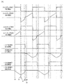
次に、関連形態のコンバータの動作の一例について説明する。まずは、図2から図6を用いてコンバータの第2回路2のスイッチング素子S5、S6をオンオフさせる動作を行う場合について説明する。図2は、第1回路1のスイッチング素子S1〜S4及び第2回路2のスイッチング素子S5、S6の駆動信号の一例を示す波形図である。図3は、第1回路1のスイッチング素子S1〜S4の電圧、電流及びトランス11の励磁電流の一例を示す波形図である。図4は、第2回路2のスイッチング素子S5、S6の電圧、電流及び一方向性素子D7、D8の電圧、電流の一例を示す波形図である。また、図5は、図3の波形図の一部の時間Tx部分を拡大した図である。図6は、各タイミングで形成される回路図である。なお、図3から図5に示す電流波形では、第1回路1のスイッチング素子S1〜S4、第2回路2のスイッチング素子S5、S6を順方向に流れる電流をプラスとし、第1回路1のスイッチング素子S1〜S4、第2回路2のスイッチング素子S5、S6を逆方向に流れる電流及び一方向性素子D7、D8を順方向に流れる電流をマイナスとしている。
Next, an example of the operation of the converter in the related form will be described. First, the case where the operation | movement which turns on / off switching element S5, S6 of the
時刻t1で、組となる第1回路1のスイッチング素子S1及びS4にオン信号を与えられたとする。第2回路2のスイッチング素子S6のオン信号は、時刻t1以前にすでに与えられているとする。そうすると、スイッチ素子Q1、Q4及びスイッチ素子Q6は順方向に導通する。この状態では、図6(a)に示されるように、第1端子T1及び第2端子T2側から供給される入力電力によって、電流が、第1端子T1側からスイッチ素子Q1、インダクタンス手段L、1次巻線11a、スイッチ素子Q4、第2端子T2側に流れる。トランス11の2次巻線11b側では、2次巻線11b、スイッチ素子Q6、一方向性素子D8を通じて電流が流れ、2次巻線11b側は短絡状態となる。このため、第1端子T1及び第2端子T2側から供給される入力電力によって、インダクタンス手段Lにエネルギーが蓄積される。また、コンデンサ17からは、第3端子T3、第4端子T4側へ電力が供給される。
Assume that an ON signal is given to the switching elements S1 and S4 of the
時刻t2で、例えば、第2回路の出力電圧検出手段18によって検出された第3端子T3、第4端子T4間の電圧検出値が目標値に近づくように制御回路3で決めたタイミングで第2回路2のスイッチング素子S6にオフ信号が与えられたとすると、インダクタンス手段Lに蓄積されたエネルギーによる第2回路2の出力側への供給が開始される。図6(b)に示すように、トランス11の1次巻線11a側は時刻t1から継続して同じ経路で電流が流れるが、2次巻線11b側ではスイッチ素子Q6がオフ状態となる。図4に示すように、この時刻t2では、第2回路2のスイッチング素子S6に大きな電流が流れる状態でスイッチ素子Q6をオフさせるのでスイッチング損失が問題となる。このスイッチング損失を減らす手段として、スイッチング素子S6のオフ時のスイッチング素子S6の両端電圧を低くさせることが考えられる。
At time t2, for example, the second timing is determined by the
本関連形態では、スイッチ素子Q6に対して並列コンデンサC6と第4コンデンサCdとを並列に接続してコンデンサの容量を大きくしている。同様に、スイッチ素子Q5に対して並列コンデンサC5と第3コンデンサCcとを並列に接続してコンデンサの容量を大きくしている。時刻t2でスイッチ素子Q6がオフすると、図6(b)に示すように、2次巻線11b側では、オフしたスイッチ素子Q6に並列に接続された並列コンデンサC6及び第4コンデンサCdを充電する方向に、電流が2次巻線11bから並列コンデンサC6及び第4コンデンサCd、一方向性素子D8を流れる。一方、並列コンデンサC5及び第4コンデンサCcからは、第3端子T3、第4端子T4側、一方向性素子D8、2次巻線11bを介して放電電流が流れる。コンデンサ容量を大きくしたことによって、並列コンデンサC6及び第4コンデンサCd、並列コンデンサC5及び第3コンデンサCcの充放電動作による第2回路2のスイッチング素子S6の両端電圧の上昇を緩やかにすることができる。このため、第2回路2のスイッチング素子S6のオフ時のスイッチング損失を低減させることができる。
In this related embodiment, the parallel capacitor C6 and the fourth capacitor Cd are connected in parallel to the switch element Q6 to increase the capacitance of the capacitor. Similarly, a parallel capacitor C5 and a third capacitor Cc are connected in parallel to the switch element Q5 to increase the capacitance of the capacitor. When the switch element Q6 is turned off at time t2, as shown in FIG. 6B, on the secondary winding 11b side, the parallel capacitor C6 and the fourth capacitor Cd connected in parallel to the turned off switch element Q6 are charged. In the direction, current flows from the secondary winding 11b through the parallel capacitor C6, the fourth capacitor Cd, and the unidirectional element D8. On the other hand, a discharge current flows from the parallel capacitor C5 and the fourth capacitor Cc through the third terminal T3, the fourth terminal T4 side, the unidirectional element D8, and the secondary winding 11b. By increasing the capacitor capacity, it is possible to moderate the rise in the voltage across the switching element S6 of the
時刻t3で第2回路2の並列コンデンサC6及び第4コンデンサCdと並列コンデンサC5及び第3コンデンサCcとの充放電が終わると、図6(c)に示すように、一方向性素子D5が導通する。2次巻線11b側の電流は、2次巻線11bから、一方向性素子D5、第3端子T3、第4端子T4側、一方向性素子D8を介して流れる。上述の時刻t1から時刻t2の間にインダクタンス手段Lに蓄積されたエネルギーが第2回路2の出力側へ供給される。なお、上述のインダクタンス手段Lに蓄積されたエネルギーによる第2回路2出力側へ供給では、第3端子T3、第4端子T4の先に接続される負荷への供給の他に、時刻t1から時刻t2の間に放電されたコンデンサ17を充電する。また、1次巻線11a側の電流は、時刻t1からスイッチ素子Q4がオフする時刻t4までの期間は同じ電流経路で流れ続ける。
When charging / discharging of the parallel capacitor C6 and the fourth capacitor Cd and the parallel capacitor C5 and the third capacitor Cc of the
時刻t4で、組となる第1回路1のスイッチング素子S1、S4のうち、先にオフさせる第1回路1のスイッチング素子S4に制御回路3からオフ信号が与えられる。このため、図3に示すように、電流値が比較的大きな状態でスイッチ素子Q4オフするため、第1回路1のスイッチング素子S4のオフ時にスイッチング損失が生じる。このスイッチング損失を減らす手段として、第1回路1のスイッチング素子S4のオフ時の第1回路1のスイッチング素子S4の両端電圧を低くさせることが考えられる。
At time t4, the
本関連形態では、スイッチ素子Q4に対して並列コンデンサC4の他に第2コンデンサCbも並列に接続してコンデンサの容量を大きくしている。同様に、スイッチ素子Q3に対して並列コンデンサC3の他に第1コンデンサCaも並列に接続してコンデンサの容量を大きくしている。このため、時刻t4でスイッチ素子Q4がオフすると、図6(d)に示すように、1次巻線11a側では、オフしたスイッチ素子Q4に並列に接続された並列コンデンサC4及び第2コンデンサCbを充電する方向に、電流がインダクタンス手段L、1次巻線11a、並列コンデンサC4及び第2コンデンサCb、第2端子T2、第1端子T1側からスイッチ素子Q1を通じて流れる。一方、並列コンデンサC3及び第1コンデンサCaからは、スイッチ素子Q1、インダクタンス手段L、1次巻線11aを通じて放電電流が流れる。コンデンサ容量を大きくしたことで、並列コンデンサC4及び第2コンデンサCb、並列コンデンサC3及び第1コンデンサCaの充放電動作によるスイッチング素子S4の両端電圧上昇を緩やかにさせることができる。よって、第1回路1のスイッチング素子S4のオフ時のスイッチング損失を低減させることができる。
In this related embodiment, in addition to the parallel capacitor C4, the second capacitor Cb is also connected in parallel to the switch element Q4 to increase the capacitance of the capacitor. Similarly, in addition to the parallel capacitor C3, the first capacitor Ca is connected in parallel to the switch element Q3 to increase the capacitance of the capacitor. Therefore, when the switch element Q4 is turned off at time t4, as shown in FIG. 6D, on the primary winding 11a side, the parallel capacitor C4 and the second capacitor Cb connected in parallel to the turned off switch element Q4. Current flows in the direction of charging the inductance means L, the primary winding 11a, the parallel capacitor C4 and the second capacitor Cb, the second terminal T2, and the first terminal T1 through the switch element Q1. On the other hand, a discharge current flows from the parallel capacitor C3 and the first capacitor Ca through the switch element Q1, the inductance means L, and the primary winding 11a. By increasing the capacitor capacity, it is possible to moderately increase the voltage across the switching element S4 due to the charge / discharge operation of the parallel capacitor C4 and the second capacitor Cb, the parallel capacitor C3 and the first capacitor Ca. Therefore, the switching loss when the switching element S4 of the
時刻t5で並列コンデンサC3及び第1コンデンサCaの放電、並列コンデンサC4及び第2コンデンサCbの充電が終わると、図6(e)に示すように、スイッチ素子Q3に並列に接続された逆並列ダイオードD3が導通する。1次巻線11a側では、インダクタンス手段Lに蓄積されたエネルギー及びトランス11の励磁電流によって、時刻t5の直前に1次巻線11a、インダクタンス手段Lに流れていた電流と同じ方向に、インダクタンス手段L、1次巻線11aから逆並列ダイオードD3、スイッチ素子Q1を通じて電流が流れる。なお、2次巻線11b側の電流は、時刻t3から継続して2次巻線11b、一方向性素子D5、第3端子T3側、第4端子T4側、一方向性素子D8を通じて流れている。この2次巻線11b側の電流経路に流れる期間は、一方向性素子D5の導通時から後に一方向性素子D5に流れる電流がほぼゼロになるまで続く。
When the discharge of the parallel capacitor C3 and the first capacitor Ca and the charge of the parallel capacitor C4 and the second capacitor Cb are finished at time t5, as shown in FIG. 6E, the antiparallel diode connected in parallel to the switch element Q3. D3 conducts. On the primary winding 11a side, due to the energy accumulated in the inductance means L and the exciting current of the
時刻t6では、組となる第1回路1のスイッチング素子S1、S4のうち、後にオフさせるスイッチング素子S1の駆動信号をオフ信号にする。スイッチ素子Q1がオフするため、時刻t6の直前に流れていたトランスの励磁電流によって、1次巻線11aから逆並列ダイオードD3、並列コンデンサC1、インダクタンス手段Lを通じて電流が流れ、並列コンデンサC1を充電する。一方、並列コンデンサC2からは、インダクタンス手段L、1次巻線11a、逆並列ダイオードD3、第1端子T1側、第2端子T2側を通じて放電電流が流れる。このとき、スイッチ素子Q1に電流がまだ流れている状態でオフさせることになるが、この電流を、非常に値の小さなトランス11の励磁電流にすることができる。よって、スイッチング素子S1は後からオフさせることでオフ時の電流値を小さくすることができるので、先にオフさせるスイッチ素子Q4のオフ時と比べて、スイッチング損失を小さくすることができる。
At time t6, among the switching elements S1 and S4 of the
時刻t7で並列コンデンサC1、C2の充放電が終わると、図6(g)に示すように、逆並列ダイオードD2が導通する。1次巻線11a側ではトランス11の励磁電流によって、時刻t7の直前に1次巻線11aに流れていた電流と同じ方向に、1次巻線11aから、逆並列ダイオードD3、第1端子T1側、第2端子T2側、逆並列ダイオードD2、インダクタンス手段Lを通じて電流が流れる。なお、2次巻線11b側の電流は、時刻t3から継続して2次巻線11b、一方向性素子D5、第3端子T3側、第4端子T4側、一方向性素子D8を通じて流れている。この2次巻線11b側の電流経路に流れる期間は、一方向性素子D5の導通時から後に一方向性素子D5に流れる電流がほぼゼロになるまで続く。
When the charging and discharging of the parallel capacitors C1 and C2 are completed at time t7, the antiparallel diode D2 is turned on as shown in FIG. On the primary winding 11a side, the anti-parallel diode D3 and the first terminal T1 from the primary winding 11a in the same direction as the current flowing in the primary winding 11a immediately before time t7 due to the exciting current of the
時刻t8で他方の組となる第1回路1のスイッチング素子S2、S3の駆動信号をオン信号にする。図6(h)に示すように、1次巻線11a側では、スイッチ素子Q2及びスイッチ素子Q3が順方向に導通し、第1端子T1側、スイッチ素子Q3、1次巻線11a、インダクタンス手段L、スイッチ素子Q2、第2端子T2側を通じて電流が流れる。2次巻線11b側では、時刻t8より以前に第2回路2のスイッチング素子S5の駆動信号にオン信号が与えられており、時刻t8にはスイッチ素子Q5が順方向に導通できる状態となっている。このため、スイッチ素子Q5が順方向に導通すると、2次巻線11bから、逆並列ダイオードD7、スイッチ素子Q5を通じて電流が流れ、2次巻線11b側は短絡状態となる。よって、第1端子T1、第2端子T2間から入力された電力によってインダクタンス手段Lにエネルギーが蓄積される。
At time t8, the drive signals of the switching elements S2 and S3 of the
本関連形態では、時刻t8の直前に、スイッチ素子Q2,Q3にそれぞれ並列に接続される逆並列ダイオードD2,D3が導通しているため、図5に示されるように、第1回路1のスイッチング素子S2,S3はオン時にゼロ電圧スイッチングを実現させることができる。
In this related embodiment, the anti-parallel diodes D2 and D3 connected in parallel to the switch elements Q2 and Q3, respectively, are conducting immediately before the time t8, so that the switching of the
また、時刻t8の直前にスイッチ素子Q5に並列の一方向性素子D5が導通しているため、スイッチ素子Q5はゼロ電圧でオンさせることができる。なお、スイッチ素子Q5のゼロ電圧スイッチングを実現させるためには、第2回路2のスイッチング素子S5の駆動信号であるオン信号は、一方向性素子D5が導通している期間である時刻t3から時刻t8の期間に与えておけばよい。
In addition, since the unidirectional element D5 in parallel with the switch element Q5 is conducted immediately before time t8, the switch element Q5 can be turned on with zero voltage. In order to realize the zero voltage switching of the switching element Q5, the ON signal that is the drive signal of the switching element S5 of the
時刻t8後の他方の組となる第1回路1のスイッチング素子S2、S3の動作については、上述の組となるスイッチング素子S1、S4の時刻t1から時刻t8と同様に動作させる。すなわち、スイッチ素子Q2及びスイッチ素子Q3が導通している期間に、例えば、第2回路2の出力側である第3端子T3、第4端子T4間の電圧検出値が所定値になるように制御回路3で決めたタイミングで第2回路2のスイッチング素子S5にオフ信号を与える。これにより、インダクタンス手段Lに蓄積されたエネルギーを第3端子T3、第4端子T4側に供給する。その後、組となるスイッチング素子S2、S3のうち第1コンデンサCaが並列に接続されたスイッチ素子Q3を先にオフさせ、後にスイッチ素子Q2をオフさせる。
The operations of the switching elements S2 and S3 of the
なお、本関連形態では、図1に示すように、後にオフさせる第1回路1のスイッチング素子S1、S2が直列に接続されている。この後にオフさせるスイッチング素子S1、S2についてゼロ電圧スイッチングを実現させるために、例えば、スイッチング素子S1をオフさせる場合、これと同じ第1レグにある他方の下アームのスイッチング素子S2の両端電圧をゼロに下げてからスイッチ素子Q2にオン信号を与える。ここで、スイッチ素子Q1にオフ信号を与えてからスイッチ素子Q2にオン信号を与えるまで期間、すなわちスイッチング素子S1、S2を共にオフさせる期間をTdとする。
In this related embodiment, as shown in FIG. 1, the switching elements S1 and S2 of the
このスイッチング素子S2の両端電圧をゼロに下げる、つまりコンデンサC2電圧がゼロになるまで放電させる放電動作は上述の励磁電流が流れることによる。よって、後にオフさせるスイッチング素子S2のゼロ電圧スイッチングを実現させるためには、まず励磁電流をスイッチング素子S2の両端電圧をゼロまで下げることができる大きさにする必要がある。さらに、励磁電流によってスイッチング素子S2の両端電圧をゼロまで下げることができるようなスイッチング素子S1、S2を共にオフさせる期間Tdを設ける必要がある。後にオフさせる第1回路1のスイッチング素子S1について、ゼロ電圧スイッチングを実現させる場合も同様である。スイッチング素子S1の両端電圧をゼロまで下げることができるような大きさの励磁電流とスイッチング素子S1、S2を共にオフさせる期間Tdを設ける必要がある。
The discharge operation for reducing the voltage across the switching element S2 to zero, that is, discharging until the capacitor C2 voltage becomes zero, is due to the above-described excitation current flowing. Therefore, in order to realize zero voltage switching of the switching element S2 to be turned off later, first, it is necessary to make the excitation current large enough to reduce the voltage across the switching element S2 to zero. Furthermore, it is necessary to provide a period Td during which both the switching elements S1 and S2 can be turned off so that the voltage across the switching element S2 can be reduced to zero by the excitation current. The same applies to the case where zero voltage switching is realized for the switching element S1 of the
なお、第1回路1のスイッチング素子S1、S2を共にオフさせる期間Tdを大きな値に設定すると、スイッチング素子S1又はS2の両端電圧がゼロまで下がった後に再度電圧が上昇してしまう、つまりコンデンサC1又はC2がゼロまで放電された後に充電されてしまうことがある。このため、スイッチング素子S1、S2を共にオフさせる期間Tdは、スイッチング素子S1又はS2の両端電圧がゼロまで下がる期間程度とするのが好ましい。また、後にオフさせるスイッチ素子Q1,Q2に並列に接続される並列コンデンサC1,C2は、スイッチング素子S1、S2内蔵の寄生容量を利用してもよい。ただし、寄生容量はもともと小さい容量の上、部品によってはバラツキがあり、本発明の動作として寄生容量だけでは不十分な場合もある。このような場合、スイッチング素子S1、S2内蔵の寄生容量に別付けのコンデンサを並列に接続させ、これらの合成容量を上記並列コンデンサC1,C2としてもよい。
If the period Td during which both the switching elements S1 and S2 of the
次に、図1のコンバータ回路図及び図7から図10を用いて、第3端子T3及び第4端子T4間側に出力される電圧を上述の第2回路2のスイッチング素子S5、S6をオンオフさせる動作で得られる出力電圧よりも低くさせる場合に、第2回路2をフルブリッジの整流回路として機能させる動作について説明する。図7は、この動作での第1回路1のスイッチング素子S1〜S4及び第2回路2のスイッチング素子S5、S6の駆動信号の一例を示す波形図である。図8は、この動作での第1回路1のスイッチング素子S1〜S4の電圧、電流及びトランス11の励磁電流の一例を示す波形図である。図9は、この動作での第2回路2の一方向性素子D5〜D8の電圧、電流の一例を示す波形図である。また、図10は、関連形態のコンバータのこの動作について各タイミングで形成される回路図である。なお、図8、図9に示す電流波形では、第1回路1のスイッチング素子S1〜S4を順方向に流れる電流をプラスとし、第1回路1のスイッチング素子S1〜S4を逆方向に流れる電流及び一方向性素子D5〜D8を順方向に流れる電流をマイナスとしている。
Next, referring to the converter circuit diagram of FIG. 1 and FIGS. 7 to 10, the voltage output to the side between the third terminal T3 and the fourth terminal T4 is turned on / off for the switching elements S5 and S6 of the
この動作の場合は、図1のコンバータ回路は、第2回路2のブリッジ接続回路は一方向性素子D5〜D8が導通するフルブリッジの整流回路として機能する。このため、実施形態1のコンバータは少なくとも第2回路2は一方向性素子D5〜D8があればよいので、図7に示すように、第2回路2のスイッチング素子S5及びS6の駆動信号にはオン信号は与えていない。
In the case of this operation, the converter circuit of FIG. 1 functions as a full-bridge rectifier circuit in which the bridge connection circuit of the
時刻t21は、組となる第1回路1のスイッチング素子S1及びS4にオン信号にオン信号を与える時点である。このとき、第2回路2のスイッチング素子S5及びS6にはオン信号は与えない。図10(a)に示すように、トランス11の1次巻線11a側では、電流が、第1端子T1側から、スイッチ素子Q1、インダクタンス手段L、1次巻線11a、スイッチ素子Q4、第2端子T2側に流れる。トランス11の2次巻線11b側では、2次巻線11bから、一方向性素子D5、第3端子T3、第4端子T4側から、一方向性素子D8を通じて電流が流れる。第1端子T1及び第2端子T2側から供給される入力電力は、インダクタンス手段Lを介して第3端子T3、第4端子T4側に供給される。
Time t21 is a time point at which an ON signal is given to the ON signal to the switching elements S1 and S4 of the
時刻t22で、例えば、第2回路の出力電圧検出手段18で検出された第3端子T3、第4端子T4間の電圧検出値が目標値に近づくように、制御回路3は、組となる第1回路1のスイッチング素子S1、S4のうち先にオフさせるスイッチング素子S4にオフ信号を与える。このため、図8に示すように、電流値が比較的大きな状態でスイッチ素子Q4がオフするため、スイッチング素子S4のオフ時にスイッチング損失が生じる。本関連形態では、上記の第2回路2のスイッチング素子S5、S6をオンオフさせる動作で説明したように、スイッチ素子Q4に対して並列コンデンサC4の他に第2コンデンサCbも並列に接続してコンデンサの容量を大きくしている。同様に、スイッチ素子Q3に対して並列コンデンサC3の他に第1コンデンサCaも並列に接続してコンデンサの容量を大きくしている。
At time t22, for example, the
このため、時刻t22でスイッチ素子Q4がオフすると、図10(b)に示すように、1次巻線11a側では、オフしたスイッチ素子Q4に並列に接続された並列コンデンサC4及び第2コンデンサCbを充電する方向に、インダクタンス手段L、1次巻線11a、並列コンデンサC4及び第2コンデンサCb、第2端子T2、第1端子T1側からスイッチ素子Q1を通じて電流が流れる。一方、並列コンデンサC3及び第1コンデンサCaからは、スイッチ素子Q1、インダクタンス手段L、1次巻線11aを通じて放電電流が流れる。先にオフさせる第1回路1のスイッチング素子S4、S3に並列に接続されるコンデンサの容量を大きくし、スイッチング素子S4の両端電圧の上昇を緩やかにさせることで、第1回路1のスイッチング素子S4のオフ時のスイッチング損失を低減させている。
Therefore, when the switch element Q4 is turned off at time t22, as shown in FIG. 10B, on the primary winding 11a side, the parallel capacitor C4 and the second capacitor Cb connected in parallel to the turned off switch element Q4. Current flows in the direction of charging the inductor L, the primary winding 11a, the parallel capacitor C4 and the second capacitor Cb, the second terminal T2, and the first terminal T1 through the switch element Q1. On the other hand, a discharge current flows from the parallel capacitor C3 and the first capacitor Ca through the switch element Q1, the inductance means L, and the primary winding 11a. The capacitance of the capacitor connected in parallel to the switching elements S4 and S3 of the
時刻t23で並列コンデンサC3及び第1コンデンサCaの放電、並列コンデンサC4及び第2コンデンサCbの充電が終わると、図10(c)に示すように、スイッチ素子Q3に並列に接続された逆並列ダイオードD3が導通する。1次巻線11a側ではインダクタンス手段Lに蓄積されたエネルギー及びトランス11の励磁電流によって、時刻t5の直前に1次巻線11a、インダクタンス手段Lに流れていた電流と同じ方向に、インダクタンス手段L、1次巻線11aから逆並列ダイオードD3、スイッチ素子Q1を通じて電流が流れる。なお、2次巻線11b側の電流は、時刻t21から継続して2次巻線11b、一方向性素子D5、第3端子T3側、第4端子T4側、一方向性素子D8を通じて流れている。
When the discharge of the parallel capacitor C3 and the first capacitor Ca and the charge of the parallel capacitor C4 and the second capacitor Cb are finished at time t23, as shown in FIG. 10C, the antiparallel diode connected in parallel to the switch element Q3. D3 conducts. On the primary winding 11a side, due to the energy accumulated in the inductance means L and the exciting current of the
時刻t24では、組となる第1回路1のスイッチング素子S1、S4のうち、後にオフさせるスイッチング素子S1の駆動信号をオフ信号にする。スイッチ素子Q1がオフするため、時刻t23の直前に流れていたトランスの励磁電流によって、図10(d)に示すように、1次巻線11aから逆並列ダイオードD3、並列コンデンサC1、インダクタンス手段Lを通じて電流が流れ、並列コンデンサC1を充電する。一方、並列コンデンサC2からは、インダクタンス手段L、1次巻線11a、逆並列ダイオードD3、第1端子T1、第2端子T2側を通じて放電電流が流れる。このとき、スイッチ素子Q1に電流がまだ流れている状態でオフさせることになるが、先にオフさせたスイッチ素子Q4のときよりも小さい値の電流にすることができる。よって、先にオフさせるスイッチ素子Q4のオフ時と比べて、後からオフさせるスイッチ素子Q1のスイッチング損失を小さくすることができる。
At time t24, the driving signal for the switching element S1 to be turned off later among the switching elements S1 and S4 of the
時刻t25で並列コンデンサC1、C2の充放電が終わると、図10(e)に示すように、逆並列ダイオードD2が導通する。1次巻線11a側ではトランス11の励磁電流によって、時刻t25の直前に1次巻線11aに流れていた電流と同じ方向に、1次巻線11aから、逆並列ダイオードD3、第1端子T1、第2端子T2側、逆並列ダイオードD2、インダクタンス手段Lを通じて電流が流れる。なお、2次巻線11b側の電流は、時刻t21から継続して2次巻線11b、一方向性素子D5、第3端子T3側、第4端子T4側、一方向性素子D8を通じて流れている。 When the charging and discharging of the parallel capacitors C1 and C2 are completed at time t25, the antiparallel diode D2 becomes conductive as shown in FIG. On the primary winding 11a side, the anti-parallel diode D3 and the first terminal T1 from the primary winding 11a in the same direction as the current flowing in the primary winding 11a immediately before time t25 due to the exciting current of the transformer 11 A current flows through the second terminal T2 side, the antiparallel diode D2, and the inductance means L. The current on the secondary winding 11b side continues from time t21 and flows through the secondary winding 11b, the unidirectional element D5, the third terminal T3 side, the fourth terminal T4 side, and the unidirectional element D8. Yes.
時刻t26で他方の組となる第1回路1のスイッチング素子S2、S3にオン信号を与える。図10(f)に示すように、1次巻線11a側では、スイッチ素子Q2及びスイッチ素子Q3が順方向に導通し、第1端子T1側、スイッチ素子Q3、1次巻線11a、インダクタンス手段L、スイッチ素子Q2、第2端子T2側を通じて電流が流れる。1次巻線11aに流れる電流が今までと逆向きになるので、2次巻線11b側では、一方向性素子D6、一方向性素子D7が順方向に導通し、2次巻線11bから、一方向性素子D7、第3端子T3、第4端子T4側から一方向性素子D6を通じて電流が流れる。図10(a)の場合と同様に、第1端子T1、第2端子T2間から入力された電力は、インダクタンス手段Lを介して第3端子T3、第4端子T4側に供給される。
At time t26, an ON signal is given to the switching elements S2 and S3 of the
上述の第2回路2のスイッチング素子S5、S6をオンオフさせる動作の場合と同様に、第2回路2のブリッジ接続回路をフルブリッジの整流回路として機能させる動作でも、時刻t26の直前に、スイッチ素子Q2,Q3にそれぞれ並列に接続される逆並列ダイオードD2,D3が導通しているため、図8に示されるように、第1回路1のスイッチング素子S2,S3はオン時にゼロ電圧スイッチングを実現させることができる。
As in the case of the operation of turning on and off the switching elements S5 and S6 of the
時刻t26後の他方の組となる第1回路1のスイッチング素子S2、S3の動作ついては、上述の組となるスイッチング素子S1、S4の時刻t21から時刻t26と同様に動作させる。すなわち、例えば、第3端子T3、第4端子T4間の出力電圧が所望の値となるように、制御回路3は、組となるスイッチング素子S2、S3のうち第1コンデンサCaが並列に接続されたスイッチ素子Q3を先にオフさせ、後にスイッチ素子Q2をオフさせる。
The operation of the switching elements S2 and S3 of the
上記の関連形態のコンバータでは、制御回路3は、上述の第2回路2のブリッジ接続回路をフルブリッジの整流回路として機能させる動作を行っている場合において、第1回路のスイッチング素子のパルス幅や周波数を変調させても前記第3端子T3、第4端子T4間側から出力される電圧の検出値が目標値に近づかない場合は、第2回路2のスイッチング素子S5、S6をオンオフさせる動作に切り替える。逆に、制御回路3は、上述の第2回路2のスイッチング素子S5、S6をオンオフさせる動作を行っている場合において、第2回路2のスイッチング素子S5、S6のパルス幅や周波数を変調させても第3端子T3、第4端子T4間側から出力される電圧の検出値が目標値に近づかない場合は、第2回路2のブリッジ接続回路をフルブリッジの整流回路として機能させる動作に切り替える。2つの動作を切り替えることで、トランス11の巻数比などの回路定数や負荷条件にとらわれずに、広範囲な入出力電圧電流に対応させることができる。
In the converter according to the related embodiment, the
なお、上述の第2回路2のスイッチング素子S5、S6をオンオフさせる動作の場合と同様に、第2回路2のブリッジ接続回路をフルブリッジの整流回路として機能させる動作でも、第1回路1の組となるスイッチ素子のうち、先にオフさせるスイッチ素子に並列に接続されるコンデンサの容量が、後にオフさせるスイッチ素子に並列に接続されるコンデンサの容量よりも大きくなるようにする。また、後にオフさせる第1回路1のスイッチング素子S1、S2についてゼロ電圧スイッチングを実現させるために、まず励磁電流をスイッチング素子S2又はS1の両端電圧をゼロまで下げることができる大きさにする必要がある。さらに、励磁電流によってスイッチング素子S2又はS1の両端電圧をゼロまで下げることができるようなスイッチング素子S1、S2を共にオフさせる期間Tdを設ける必要がある。
Note that, as in the case of the operation of turning on and off the switching elements S5 and S6 of the
第1回路1のスイッチング素子S1、S2を共にオフさせる期間Tdは、スイッチング素子S1又はS2の両端電圧がゼロまで下がる期間程度とするのが好ましい。
The period Td during which both the switching elements S1 and S2 of the
なお、図2、図7では、時刻t8、時刻t26に、第1回路1のスイッチング素子S2、S3の駆動信号であるオン信号を同時に与えており、かつ、スイッチ素子Q2及びスイッチ素子Q3が順方向に導通し始めている動作の一例を示した。しかし、上記の実施形態の動作の一例に限定されることなく、スイッチング素子S2、S3のオン信号を与える時点は同時でなくてもよい。また、スイッチング素子S2、S3のオン信号を与える時点は、逆並列ダイオードD2、D3が導通している期間であってもよい。この場合は、スイッチング素子S2、S3のオン信号を与える時点とスイッチ素子Q2及びスイッチ素子Q3が順方向に導通し始め時点は一致せず、例えば、逆並列ダイオードD2、D3を導通する電流がゼロになってからスイッチ素子Q2及びスイッチ素子Q3を順方向に電流が流れ始める。また、逆方向に電流を流したときのスイッチ素子Q2、Q3の電圧降下が順方向電流を流したときの逆並列ダイオードD2、D3の電圧降下である順電圧よりも小さい場合には、スイッチング素子S2、S3のオン信号を与え、スイッチ素子Q2、Q3を逆方向に導通させてスイッチング素子S2、S3の導通損失を低減させることができる。もう一方の組となる第1回路1のスイッチング素子S1、S4の場合についても同様である。
In FIG. 2 and FIG. 7, an ON signal that is a drive signal for the switching elements S2 and S3 of the
上記の関連形態では、組となる第1回路1のスイッチング素子S1及びS4、S2及びS3のうち第2レグ13の上下アームのスイッチング素子S4、S3を先にオフさせているが、第1レグ12の上下アームのスイッチング素子S1、S2を先にオフさせてもよい。この場合、第1コンデンサCa、第2コンデンサCbを、先にオフさせるスイッチング素子S1、S2にそれぞれ接続させる。また、先にオフさせる第1回路1のスイッチング素子を、第1レグ12と第2レグ13との上アームのスイッチング素子S1、S3、又は、第1レグ12と第2レグ13との下アームのスイッチング素子S2、S4としてもよい。この場合、第1コンデンサCa、第2コンデンサCbを、先にオフさせるスイッチング素子S1、S3又はスイッチング素子S2、S4にそれぞれ並列に接続させる。
In the above-mentioned related form, the switching elements S4 and S3 of the upper and lower arms of the
また、上記の関連形態において、図1に示した第2回路2のブリッジ接続回路内で、第3端子T3、第4端子T4間に接続されるスイッチング素子S5、S6の直列回路と一方向性素子D7,D8の直列回路との位置が入れ替わってもよい。この場合も、第3コンデンサCc、第4コンデンサCdは、オンオフさせる第2回路2のスイッチング素子S5、S6にそれぞれ並列に接続される。また、第2回路2において一方向性素子D7又はD8と第2回路2のスイッチング素子S5又はS6との直列回路をそれぞれ第3端子T3、第4端子T4間に接続する混合ブリッジ接続の回路構成にしてもよい。この場合も、第3コンデンサCc、第4コンデンサCdは、オンオフさせる第2回路2のスイッチング素子S5、S6にそれぞれ並列に接続させる。
Further, in the above-mentioned related form, the series circuit of the switching elements S5 and S6 connected between the third terminal T3 and the fourth terminal T4 in the bridge connection circuit of the
さらに、上記の実施形態1の説明では、第2回路2の一方向性素子D7、一方向性素子D8としてダイオードで示したが、この一例に限定されることなく電流を一方向へ導通させる素子であればよい。また、一方向性素子として、スイッチング素子S5、S6と同様にスイッチング素子の内部ダイオードを用いてもよい。上述の第2回路2のブリッジ接続回路をフルブリッジの整流回路として機能させる動作の説明において、一方向性素子D5、D6が導通する期間に、例えば、図1のスイッチング素子S5、S6にオン信号を与えて、スイッチ素子Q5、Q6を逆方向、すなわち一方向性素子D5、D6の順方向に導通させてもよい。逆方向に電流を流したときのスイッチ素子Q5、Q6の電圧降下が順方向電流を流したときの逆一方向性素子D5、D6の電圧降下である順電圧よりも小さい場合には、一方向性素子D5、D6の導通損失よりも低減させることができる。同様に、一方向性素子D7、D8を含むスイッチング素子S7、S8又は一方向性素子D7、D8と並列に接続したスイッチング素子S7、S8を用いた場合も、スイッチ素子Q7、Q8を逆方向に導通させて一方向性素子D7、D8の導通損失よりも低減させることができる。なお、上述のコンバータにおいて第3端子T3及び第4端子T4側間に出力される電圧を第2回路2のスイッチング素子S5、S6をオンオフさせる動作で得られる出力電圧よりも低くさせる動作のみに用いる場合は、第2回路2は少なくともフルブリッジの整流回路として動作する一方向性素子D5〜D8又は一方向性素子D5〜D8の順方向と同じ方向に電流を流せるスイッチング素子を有すればよい。
Furthermore, in the description of the first embodiment, the diode is shown as the unidirectional element D7 and the unidirectional element D8 of the
本関連形態のコンバータは、トランスの1次巻線又は2次巻線側に接続されるインダクタンス手段を用い、第2回路のスイッチング素子をオンオフさせる動作と第2回路のブリッジ接続回路をフルブリッジの整流回路として機能させる動作とを実現させることで広範囲な入出力電圧電流に対応させることができる。また、電流が流れている状態でスイッチング素子をオフさせたときに発生するスイッチング損失を低減することができ、組となる第1回路のスイッチング素子のうちの一方を後からオフさせたときに発生するスイッチング損失を低減することができる。さらに、ゼロ電圧スイッチングを実現させることでスイッチング損失の低減を図ることができる。 The converter according to this related embodiment uses inductance means connected to the primary winding or secondary winding side of the transformer, and turns on and off the switching element of the second circuit and the bridge connection circuit of the second circuit of the full bridge. By realizing the operation of functioning as a rectifier circuit, a wide range of input / output voltage currents can be handled. In addition, the switching loss that occurs when the switching element is turned off while the current is flowing can be reduced, and occurs when one of the switching elements of the first circuit to be paired is turned off later. Switching loss can be reduced. Furthermore, switching loss can be reduced by realizing zero voltage switching.
(第1の実施形態)
本実施形態及び以降の実施形態において、断りのない限り「第1回路1」とは「第1回路1−1」と「第1回路1−2」の双方に共通内容を説明するために使用する。
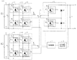
図11に、本発明の第1の実施形態に係る多入力コンバータの電気回路図を示す。図11に示される多入力コンバータは、N個(Nは2以上の整数)の1次巻線と1つの2次巻線とを有するトランス11tと、トランス11tの1次巻線11aのそれぞれに接続されるN個の第1回路1と、トランス11tの2次巻線11b側に接続される第2回路2と、インダクタンス手段Lと、制御回路3とを備える。この多入力コンバータは、各第1回路1の第1端子T1及び第2端子T2側から入力される直流を交流に変換させて第1回路1から出力し、トランス11tを介して第2回路2で交流を直流に変換して出力側の第3端子T3、第4端子T4側へ電力を供給する。図11の多入力コンバータではN=2の場合を説明しているが、Nが2より大きい場合も同様である。
(First embodiment)
In this embodiment and the following embodiments, “
FIG. 11 shows an electric circuit diagram of the multi-input converter according to the first embodiment of the present invention. The multi-input converter shown in FIG. 11 includes a
各第1回路1の構成及び第2回路の構成は、関連形態で説明した第1回路1の構成及び第2回路2の構成と同じである。トランス11tの1次巻線の数と第1回路1の数が多数であることが本実施形態と関連形態との回路構成上の相違点である。なお、トランス11tのそれぞれの1次巻線の巻き数は同じであっても異なっていてもよい。また、それぞれの第1回路1の第1端子T1及び第2端子T2側から入力される直流電圧は同じであっても異なっていてもよい。また、図11の多入力コンバータでは、インダクタンス手段Lが各第1回路1とトランス11tの1次巻線との間に配置されるが、第2回路2とトランス11tの2次巻線との間に配置してもよい。
The configuration of each
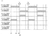
本実施形態の制御回路3は、それぞれの第1回路1のスイッチング素子S1〜S4、第2回路2のスイッチング素子S5、S6にそれぞれ駆動信号を与えて、各スイッチング素子のオンオフ制御をする。図12及び図13は、それぞれの第1回路1のスイッチング素子S1〜S4及び第2回路2のスイッチング素子S5、S6の駆動信号の一例を示す波形図である。図12は後述する「動作B」時の波形図、図13は後述する「動作A」の波形図である。1つの第1回路1と第2回路2に注視すれば、制御回路3が制御する第1回路1のスイッチング素子S1〜S4及び第2回路2のスイッチング素子S5、S6の駆動信号のタイミングは関連形態での説明通りである。
The
つまり、制御回路3が制御する駆動信号のタイミングとコンデンサ容量を大きくしたことによって、並列コンデンサC6及び第4コンデンサCd、並列コンデンサC5及び第3コンデンサCcの充放電動作による第2回路2のスイッチング素子S6及びS5の両端電圧の上昇を緩やかにすることができる。このため、第2回路2のスイッチング素子S6及びS5のオフ時のスイッチング損失を低減させることができる。また、制御回路3が制御する駆動信号のタイミングとコンデンサ容量を大きくしたことで、並列コンデンサC4及び第2コンデンサCb、並列コンデンサC3及び第1コンデンサCaの充放電動作によるスイッチング素子S4及びS3の両端電圧上昇を緩やかにさせることができる。よって、第1回路1のスイッチング素子S4及びS3のオフ時のスイッチング損失を低減させることができる。
That is, the switching element of the
また、制御回路3が制御する駆動信号のタイミングで、スイッチング素子S1及びS2を流れる電流が小さくなった後に後からオフするスイッチング素子S1及びS2をオフするので先にオフするスイッチング素子S4及びS3よりスイッチング損失を低減させることができる。
Also, since the switching elements S1 and S2 that are turned off later after the current flowing through the switching elements S1 and S2 becomes small at the timing of the drive signal controlled by the
さらに、制御回路3は、制御する駆動信号のタイミングで第1回路1毎に期間Tdを作り出している。このため、第1回路1のスイッチング素子(S1及びS2)に並列するダイオードが導通している間にスイッチング素子(S1及びS2)をオンさせるためゼロ電圧スイッチングを実現できる。
Further, the
なお、制御回路3が「前記組となる第1回路のスイッチング素子がオン状態にある期間に前記第1及び第2端子側から入力されるエネルギーを前記インダクタンス手段に蓄積させるように前記第3コンデンサ又は第4コンデンサが並列に接続された前記スイッチング素子を順方向に導通させ、前記先にオフさせる第1回路のスイッチング素子をオフする前に前記順方向に導通させていた第2回路のスイッチング素子をオフさせる」動作とは、図6のように各スイッチ素子をスイッチングさせる動作である。この動作は、第3端子T3と第4端子T4とに接続された負荷が大きな電力を要求しているときの動作であり、ここでは「動作B」と称する。
Note that the
また、制御回路3が「前記組となる第1回路のスイッチング素子がオン状態にある期間に前記第1及び第2端子側から入力されるエネルギーを前記インダクタンス手段を介して前記第3及び第4端子側に供給させるように前記第2回路のスイッチング素子を順方向に導通させない」動作とは、図10のように各スイッチ素子をスイッチングさせる動作である。この動作は、第3端子T3と第4端子T4とに接続された負荷が大きな電力を要求していないときの動作であり、ここでは「動作A」と称する。
Further, the
本実施形態の多入力コンバータは第1回路1を複数並列させている。それぞれの第1回路1で上記のスイッチング損失の低減やゼロ電圧スイッチングを可能とするために、本実施形態の多入力コンバータは第1回路1相互間で図12及び図13のようにスイッチ動作させる。
In the multi-input converter of this embodiment, a plurality of
まず、「動作B」について説明する。図12は、動作Bを行う場合の、それぞれの第1回路1のスイッチング素子S1〜S4及び第2回路2のスイッチング素子S5、S6の駆動信号の一例を示す波形図である。
制御回路3は、組となる第1回路1のスイッチ素子(例えば、Q1とQ4)がオン状態にある期間(例えば、図12のα)が、全ての第1回路1において重複するように第1回路1のスイッチング素子をパルス制御する。そして制御回路3は、第3端子T3及び第4端子T4間側から出力される電圧、電流もしくは電力の検出値又は第1端子T1及び第2端子T2間側から入力される電圧、電流又は電力の検出値が目標値に近づくように、第1回路1毎に動作Bをさせる。つまり、制御回路3は、第1回路1それぞれで組となる第1回路のスイッチング素子がオン状態にある期間に第1端子T1及び第2端子T2側から入力されるエネルギーをそれぞれのインダクタンス手段Lに蓄積させるようにスイッチ素子(例えばQ6)を順方向に導通させる(例えば図12のβ)。さらに制御回路3は、第1回路1のなかで最先に先にオフさせる第1回路1のスイッチ素子(例えば第1回路1−1のQ4)をオフする前に順方向に導通させていた第2回路2のスイッチ素子(例えばQ6)をオフさせる(例えば図12のγ)。
First, “Operation B” will be described. FIG. 12 is a waveform diagram showing an example of drive signals for the switching elements S1 to S4 of the
The
ここで、制御回路3は、第1回路1のスイッチング素子をパルス制御し、組となる第1回路のスイッチング素子がオン状態にある期間と第1回路のなかで最先に前記先にオフさせる第1回路(例えば、第1回路1−1)のスイッチング素子をオフする前に前記順方向に導通させていた第2回路のスイッチング素子(例えばS6)の導通期間との重複期間(例えば図12のδ)を、所望のエネルギーが第1端子T1及び第2端子T2側からそれぞれのインダクタンス手段Lを介して第3端子T3及び第4端子T4側に供給されるように第1回路1毎に調整することが好ましい。
Here, the
また、制御回路3は、第3端子T3及び第4端子T4間側から出力される電圧、電流もしくは電力の検出値又は第1端子T1及び第2端子T2間側から入力される電圧、電流又は電力の検出値が目標値に近づくように、第1回路毎に動作Aをさせることもできる。図13は、動作Aを行う場合の、それぞれの第1回路1のスイッチング素子S1〜S4及び第2回路2のスイッチング素子S5、S6の駆動信号の一例を示す波形図である。つまり、制御回路3は、第1回路1それぞれで組となる第1回路のスイッチング素子がオン状態にある期間(例えば、図13のα)に第1端子T1及び第2端子T2側から入力されるエネルギーをそれぞれのインダクタンス手段Lを介して第3端子T3及び第4端子T4側に供給させるように第2回路2のスイッチング素子を順方向に導通させない(第2回路2を短絡状態とし、インダクタンス手段Lにエネルギーを蓄積させない)。
Further, the
制御回路3は、第3端子T3及び第4端子T4間側から出力される電圧、電流もしくは電力の検出値又は第1端子T1及び第2端子T2間側から入力される電圧、電流又は電力の検出値が目標値に近づくように、動作Aと動作Bを適宜選択することができる。
The
制御回路3は、組となる第1回路1のスイッチング素子がオン状態にある期間に第1端子T1及び第2端子T2側から入力され、インダクタンス手段Lを介して第3端子T3及び第4端子T4側に供給させるエネルギーに比例して、第1回路1それぞれの、先にオフさせる第1回路のスイッチ素子(例えば図12のスイッチ素子Q3、Q4)をオフするタイミングを制御する(例えば図12のη)。
The
例えば、それぞれの第1回路1の第1端子T1及び第2端子T2に入力する直流電源の電圧(E1、E2)がE1>E2であったと仮定する。前述のように第1回路1のスイッチング素子(S11、S12、S21、S22)をゼロ電圧でオンさせるためにトランス11tで発生する励磁電流を利用するが、E1とE2に差がある場合、励磁電流は電圧が高い方(E1が入力される第1回路)に偏るため、他方(E2が入力される第1回路)ではゼロ電圧スイッチングに必要な励磁電流が不足することになる。このような不具合を防ぐために、制御回路3は、電圧が低い方(E2が入力される第1回路1−2)のスイッチ素子(Q3,Q4)がオフする前に電圧が高い方(E1が入力される第1回路1−1)のスイッチ素子(Q3,Q4)をオフさせる(例えば図12のη)。このようにスイッチングすることで、電圧が低い方(E2が入力される第1回路1−2)にも励磁電流が流れるようになり、ゼロ電圧スイッチングが可能になる。なお、電圧が高い方(E1が入力される第1回路1−1)のスイッチ素子(Q3,Q4)をオフしてから電圧が低い方(E2が入力される第1回路)のスイッチ素子(Q23,Q24)がオフするまでの時間は、E1とE2の電圧差に比例して長く設定する。
For example, it is assumed that the voltage (E1, E2) of the DC power source input to the first terminal T1 and the second terminal T2 of each
図14は、第1回路1の第1端子T1及び第2端子T2に入力する直流電源の電圧に差がある場合の各スイッチ素子に流れる電流と励磁電流の様子を説明する図である。電圧が低い方(E2が入力される第1回路1−2)のスイッチ素子Q4がオフする前に電圧が高い方(E1が入力される第1回路1−1)のスイッチ素子Q4をオフさせることで電圧が低い方(E2が入力される第1回路1−2)にも励磁電流が流れることが表れている。なお、破線は、電圧が低い方(E2が入力される第1回路1−2)のスイッチ素子Q4がオフする前に電圧が高い方(E1が入力される第1回路1−1)のスイッチ素子Q4をオフさせなかった場合の第1回路の電流を表している。励磁電流が電圧が高い方(E1が入力される第1回路1−1)に流れてしまい、電圧が低い方(E2が入力される第1回路1−2)は逆向きの電流となりゼロ電圧スイッチングができないことがわかる。
FIG. 14 is a diagram for explaining the state of the current flowing through each switch element and the excitation current when there is a difference in the voltage of the DC power supply input to the first terminal T1 and the second terminal T2 of the
なお、本実施形態では、トランス11tの各1次巻線の巻き数が同じ場合を説明したが、トランス11tの各1次巻線の巻き数が異なる場合も同様である。具体的には、第1回路に入力する電圧が同じであれば、トランス11tの巻き数が多い1次巻線に接続する第1回路のスイッチ素子をオフしてから巻き数が少ない1次巻線に接続する第1回路のスイッチ素子がオフするまでの時間を、1次巻線の巻き数差に応じて長く設定する。第1回路に入力する電圧が異なる場合は、第1回路に入力する電圧と1次巻線の巻き数との積に基づいて第1回路のスイッチ素子をオフする時間を決める。つまり、前記積が大きい第1回路のスイッチ素子をオフしてから前記積が小さい第1回路のスイッチ素子がオフするまでの時間を、前記積に応じて長く設定する。
In the present embodiment, the case where the number of turns of each primary winding of the
以上のように本実施形態は、図11のように簡単な回路構成で多入力可能なコンバータを実現でき、且つ図12や図13のようにスイッチング素子を制御することでスイッチング損失も低減することできる。つまり、本実施形態のコンバータは、トランスを1つとした簡単な回路構成の特許文献5や特許文献6の装置で実現できなかったスイッチング損失の低減を実現することができた。
As described above, this embodiment can realize a converter capable of multiple inputs with a simple circuit configuration as shown in FIG. 11, and can also reduce switching loss by controlling the switching elements as shown in FIGS. it can. That is, the converter according to the present embodiment can realize a reduction in switching loss that could not be realized by the devices of
(第2の実施形態)
図15に、本発明の第2の実施形態に係る双方向コンバータの電気回路図を示す。本発明の第2の実施形態に係る双方向コンバータにおいて、関連形態のコンバータと符号が同じ構成要素は、相互に同一のものを示すものとする。ここでは、主に第1の実施形態のコンバータと異なる構成及び動作について説明する。
(Second Embodiment)
FIG. 15 shows an electric circuit diagram of the bidirectional converter according to the second embodiment of the present invention. In the bidirectional converter according to the second embodiment of the present invention, components having the same reference numerals as those of the converter of the related embodiment indicate the same components. Here, the configuration and operation different from the converter of the first embodiment will be mainly described.
第2の実施形態に係る双方向コンバータでは、双方向で動作させるため、第2回路は、第1回路と同様の構成になるようにする。このため、図15では、第2回路22は、スイッチング素子を2つのレグの上下アームとした回路構造にする。また、第2回路22のスイッチング素子S7、S8にも駆動信号を与えることからも、ここでは、制御回路23とする。なお、第1回路1の第1レグ12、第2レグ13及び第2回路22の第3レグ14については、関連形態で述べた図1に示す構成と同様である。また、図1と同様に、図15では、インダクタンス手段Lは、1次巻線11a側に接続されているが、2次巻線11b側に接続させてもよい。
In the bidirectional converter according to the second embodiment, the second circuit is configured in the same manner as the first circuit in order to operate in both directions. For this reason, in FIG. 15, the
第1回路1で組となる第1回路1のスイッチング素子S1とS4、S2とS3のうち、先にオフさせる一方のレグの上下アーム、ここでは第1レグ12の上下アームのスイッチング素子S3、S4が直列に接続される。先にオフさせる第1回路1のスイッチング素子S3、S4には、それぞれ第1、第2コンデンサCa、Cbが並列に接続される。
Of the switching elements S1 and S4 and S2 and S3 of the
図15に示すように、第2回路22の第3レグ24、第4レグ25は、第3端子T3と第4端子T4との間にそれぞれ並列に接続される。第3レグ24、第4レグ25は、上下アームをスイッチング素子S5〜S8で構成したフルブリッジ接続の回路となる。また、スイッチング素子S5〜S8は、スイッチ素子Q5〜Q8と一方向性素子D5〜D8と並列コンデンサC5〜C8とがそれぞれ並列に接続される。なお、関連形態と同様に、一方向性素子D5〜D8は、図15に示したように第2回路22のスイッチング素子S5〜S8の内蔵ダイオードを用いてもよく、第2回路22のスイッチング素子S5〜S8とは別に外付けされたダイオードを用いてもよく、またはこれらの組み合わせであってもよい。同様に、並列コンデンサC5〜C8は、図15に示したように第2回路22のスイッチング素子S5〜S8の寄生容量を用いてもよく、第2回路22のスイッチング素子S5〜S8とは別に外付けされたコンデンサを用いてもよく、またはこれらの組み合わせであってもよい。
As shown in FIG. 15, the
第2回路22から第1回路1側へ電力を供給する場合に、第2回路22で組となるスイッチング素子S5とS8、S6とS7のうち、先にオフさせる一方のレグの上下アーム、ここでは第3レグ24の上下アームのスイッチング素子S5、S6が直列に接続される。先にオフさせるスイッチング素子S5、S6には、それぞれ第3、第4コンデンサCc、Cdが並列に接続される。
When supplying power from the
第1回路1から第2回路22側へ電力を供給する場合は、上記の実施形態1で述べたのと同様の動作を行う。また、第2回路22から第1回路1側へ電力を供給する場合、制御回路23は、第2回路22で組となるスイッチング素子S5とS8、S6とS7のうち、第3、第4コンデンサCc,Cdがそれぞれ並列に接続されたスイッチング素子S5、S6を先にオフさせる。
When power is supplied from the
第1回路1から第2回路22側へ電力を供給するときに、出力側となる第2回路2のスイッチング素子をオンオフさせる場合は、関連形態と同様に、制御回路23は、第2回路22の第3、第4コンデンサCc、Cdが並列に接続されたスイッチング素子S5,S6をオンオフさせる。また、第2回路22から第1回路1側へ電力を供給する場合ときに、出力側となる第1回路1のスイッチング素子をオンオフさせる場合は、制御回路23は、第1回路1のうち第1、第2コンデンサCa,Cbがそれぞれ並列に接続された第1回路1のスイッチング素子S3,S4をオンオフさせる。なお、出力側の電圧を第2回路又は第1回路のスイッチング素子をオンオフさせる動作で得られる出力電圧よりも低くさせる動作の場合は、関連形態で述べたように、出力側の第2回路22のスイッチング素子S5〜S8又は第1回路1のスイッチング素子S1〜S4は整流回路として機能する。
When the power is supplied from the
また、制御回路23は、出力側の第2回路22又は第1回路1を整流回路として機能させる動作を行っている場合において、第1回路1又は第2回路22のスイッチング素子のパルス幅や周波数を変調させても第3端子T3、第4端子T4間又は第1端子T1、第2端子T2間側から出力される電圧の検出値が目標値に近づかない場合は、出力側の第2回路22又は第1回路1のスイッチング素子をオンオフさせる動作に切り替える。
In addition, when the
具体的には、第1回路1から第2回路22側へ電力を供給する場合に、制御回路23は、組となる第1回路のスイッチング素子S1とS4又はS2とS4がオン状態にある期間に第1端子T1及び第2端子T2側から入力されるエネルギーをインダクタンス手段Lを介して第3端子T3及び第4端子T4側に供給させるように第1回路1のスイッチング素子S4又はS3をパルス制御する。このときに、第2回路22のスイッチング素子S5及びS6を順方向に導通させない。この状態から、組となる第1回路1のスイッチング素子S1とS4又はS2とS4がオン状態にある期間に第1端子T1及び第2端子T2側から入力されるエネルギーをインダクタンス手段Lに蓄積させるように第3コンデンサCc又は第4コンデンサCdが並列に接続された第2回路22のスイッチング素子S6又はS5を順方向に導通させる。そして、先にオフさせる第1回路1のスイッチング素子S4又はS3をオフする前に順方向に導通させている第2回路22のスイッチング素子S6又はS5をオフさせる動作に切り替える。
Specifically, when power is supplied from the
逆に、制御回路23は、出力側の第2回路22又は第1回路1のスイッチング素子をオンオフさせる動作を行っている場合において、第2回路22又は第1回路1のスイッチング素子のパルス幅や周波数を変調させても第3端子T3、第4端子T4間又は第1端子T1、第2端子T2間側から出力される電圧の検出値が目標値に近づかない場合は、出力側の第2回路22又は第1回路1を整流回路として機能させる動作に切り替える。
Conversely, when the
具体的には、第1回路1から第2回路22側へ電力を供給する場合に、制御回路23は、組となる第1回路1のスイッチング素子S1とS4又はS2とS3とがオン状態にある期間に第1端子T1及び第2端子T2側から入力されるエネルギーをインダクタンス手段Lに蓄積させるように第3コンデンサCc又は第4コンデンサCdが並列に接続された第2回路22のスイッチング素子S6又はS5を順方向に導通させる。このとき、先にオフさせる第1回路1のスイッチング素子S4又はS3をオフする前に順方向に導通させている第2回路22のスイッチング素子S6又はS5をオフさせる第2回路22のスイッチング素子S6又はS5のパルス制御を行っているとする。次に、この動作から、組となる第1回路1のスイッチング素子S1とS4又はS2とS4とがオン状態にある期間に第1端子T1及び第2端子T2側から入力されるエネルギーをインダクタンス手段Lを介して第3端子T3及び第4端子T4側に供給させるように第2回路22のスイッチング素子を順方向に導通させない動作に切り替える。
Specifically, when power is supplied from the
上述のように動作を切り替えて、第3、第4端子間又は第1、第2端子間側から出力される電圧の検出値を目標値に近づけさせるように、第1回路、第2回路のスイッチング素子のパルス制御を行う。2つの動作を切り替えることで、トランスの巻数比などの回路定数や負荷条件にとらわれずに、広範囲な入出力電圧電流に対応させることができる。 As described above, the operation of the first circuit and the second circuit is switched so that the detected value of the voltage output from the third and fourth terminals or between the first and second terminals is brought close to the target value. Performs pulse control of the switching element. By switching between the two operations, a wide range of input / output voltage currents can be handled without being limited by circuit constants such as the turns ratio of the transformer and load conditions.
上述のように本発明では、入力側の第1又は第2回路の組となるスイッチ素子のうち、先にオフさせるスイッチ素子に並列に接続されるコンデンサの容量が、後にオフさせるスイッチ素子に並列に接続されるコンデンサの容量よりも大きくなるようにする。同様に、オンオフさせる出力側の第2回路又は第1回路のスイッチング素子についても並列にコンデンサを接続する。このことにより、第1回路のスイッチング素子、第2回路のスイッチング素子のオン時、オフ時に生じるスイッチング損失を低減させている。 As described above, in the present invention, among the switch elements that form the first or second circuit set on the input side, the capacitance of the capacitor connected in parallel to the switch element that is turned off first is parallel to the switch element that is turned off later. It should be larger than the capacitance of the capacitor connected to. Similarly, a capacitor is connected in parallel to the switching element of the second circuit or the first circuit on the output side to be turned on / off. This reduces switching loss that occurs when the switching element of the first circuit and the switching element of the second circuit are turned on and off.
また、後にオフさせる第1回路1のスイッチング素子S1、S2又は第2回路22のスイッチング素子S7、S8についてゼロ電圧スイッチングを実現させるためには、例えば、第1回路1のスイッチング素子S1又は第2回路22のスイッチング素子S7をオフさせる場合、これと同じレグにある他方のアームの第1回路1のスイッチング素子S2又は第2回路22のスイッチング素子S8の両端電圧をゼロに下げてからスイッチ素子Q2又はQ8にオン信号を与える必要がある。この第1回路1のスイッチング素子S2又は第2回路22のスイッチング素子S8の両端電圧、つまりコンデンサC2又はC8電圧がゼロになるまで放電させる放電動作は上述の励磁電流が流れることによる。
In order to realize zero voltage switching for the switching elements S1 and S2 of the
よって、後にオフさせる第1回路1のスイッチング素子S2又は第2回路22のスイッチング素子S8のゼロ電圧スイッチングを実現させるためには、まず励磁電流を第1回路1のスイッチング素子S2又は第2回路22のスイッチング素子S8の両端電圧をゼロまで下げることができる大きさにする必要がある。さらに、励磁電流によって第1回路1のスイッチング素子S2又は第2回路22のスイッチング素子S8の両端電圧をゼロまで下げることができるような第1回路1のスイッチング素子S1、S2又は第2回路22のスイッチング素子S7、S8を共にオフさせる期間Tdを設ける必要がある。後にオフさせる第1回路1のスイッチング素子S1、第2回路22のスイッチング素子S7について、ゼロ電圧スイッチングを実現させる場合も同様である。第1回路1のスイッチング素子S1又は第2回路22のスイッチング素子S8の両端電圧をゼロまで下げることができるような大きさの励磁電流と第1回路1のスイッチング素子S1、S2又は第2回路22のスイッチング素子S7、S8を共にオフさせる期間Tdを設ける必要がある。
Therefore, in order to realize zero voltage switching of the switching element S2 of the
なお、第1回路1のスイッチング素子S1、S2を共にオフさせる期間Tdを大きな値に設定すると、スイッチング素子S1又はS2の両端電圧がゼロまで下がった後に再度電圧が上昇してしまう、つまりコンデンサC1又はC2がゼロまで放電された後に充電されてしまうことがある。このため、スイッチング素子S1、S2を共にオフさせる期間Tdは、スイッチング素子S1又はS2の両端電圧がゼロまで下がる期間程度とするのが好ましい。第2回路22のスイッチング素子S7、S8についても同様である。また、後にオフさせるスイッチ素子Q1,Q2に並列に接続される並列コンデンサC1,C2は、第1回路1のスイッチング素子S1、S2内蔵の寄生容量を利用してもよい。ただし、寄生容量はもともと小さい容量の上、部品によってはバラツキがあり、本発明の動作として寄生容量だけでは不十分な場合もある。このような場合、第1回路1のスイッチング素子S1、S2内蔵の寄生容量に別付けのコンデンサを並列に接続させ、これらの合成容量を上記並列コンデンサC1,C2としてもよい。第2回路22の並列コンデンサC7、C8についても同様である。
If the period Td during which both the switching elements S1 and S2 of the
以上のように本実施形態は、図15のように簡単な回路構成で多入力可能な双方向コンバータを実現でき、且つ図12や図13のようにスイッチング素子を制御することでスイッチング損失も低減することできる。つまり、本実施形態の双方向コンバータは、トランスを1つとした簡単な回路構成の特許文献5や特許文献6の装置で実現できなかったスイッチング損失の低減を実現することができた。
As described above, this embodiment can realize a bidirectional converter capable of multiple inputs with a simple circuit configuration as shown in FIG. 15, and also reduces switching loss by controlling the switching elements as shown in FIGS. Can do. That is, the bidirectional converter according to the present embodiment was able to realize a reduction in switching loss that could not be realized by the devices of
(他の実施形態)
本発明では、上述の説明において、励磁電流を適切な大きさにするためにトランス11tの1次巻線又は2次巻線に並列に設けられるインダクタンス成分も上述のトランスの励磁インダクタンスに含まれる。また、上述の説明において、トランス11tの励磁インダクタンスとこれに並列に設けられるインダクタンス成分とによる合成インダクタンスによって流れる電流も上述の励磁電流に含まれる。トランスの励磁インダクタンスは、トランスの構造において、例えば、コアのギャップ幅、巻線の巻数量、コアの材質などによって調整することができる。
(Other embodiments)
In the present invention, in the above description, an inductance component provided in parallel with the primary winding or the secondary winding of the
上記の第1、第2の実施形態では、制御回路3、23は、第2回路の出力電圧検出手段18、第1回路の出力電圧検出手段19によって検出された電圧値が目標値に近づくようにしているが、用いる検出値は出力電流値や出力電力の他にこれらの組み合わせであってもよい。同様に入力側の電圧、電流又は電力の検出値が目標値に近づくようにしてもよい。なお、一般的に、電力の検出値としては、検出された電圧及び電流を乗算した演算値を用いる。上述の出力される電圧、電流もしくは電力の検出値又は入力される電圧、電流又は電力の検出値には、これらの値にある係数を乗除算したり、ある値を加減算等したりといった演算をして得られた値も含まれる。
In the first and second embodiments described above, the
本発明は、トランスの1次巻線又は2次巻線側に接続されるインダクタンス手段を用いて、出力側の第2回路又は第1回路のスイッチング素子をオンオフさせる動作と出力側の第2回路又は第1回路を整流回路として機能させる動作とを実現させることで広範囲な入出力電圧電流に対応させることができる。また、電流が流れている状態でスイッチング素子をオフさせたときに発生するスイッチング損失を低減することができ、組となる第1回路のスイッチング素子のうちの一方を後からオフさせたときに発生するスイッチング損失を低減することができる。さらに、ゼロ電圧スイッチングを実現させることでスイッチング損失の低減を図ることができる。 The present invention uses an inductance means connected to the primary winding or secondary winding side of the transformer to turn on or off the second circuit on the output side or the switching element of the first circuit, and the second circuit on the output side. Alternatively, it is possible to cope with a wide range of input / output voltage currents by realizing the operation of causing the first circuit to function as a rectifier circuit. In addition, the switching loss that occurs when the switching element is turned off while the current is flowing can be reduced, and occurs when one of the switching elements of the first circuit to be paired is turned off later. Switching loss can be reduced. Furthermore, switching loss can be reduced by realizing zero voltage switching.
本発明の電気回路において、接続点とは電気的に接続されて同電位にある部位を言い、物理的に接続された点を言うものではない。また、本発明のコンバータ及び双方向コンバータにおける各部の構成、構造、数、配置、形状、材質などに関しては、上記具体例に限定されず、当業者が適宜選択的に採用したものも、本発明の要旨を包含する限り、本発明の範囲に包含される。 In the electric circuit of the present invention, the connection point refers to a portion that is electrically connected and at the same potential, and does not refer to a point that is physically connected. Further, the configuration, structure, number, arrangement, shape, material, and the like of each part in the converter and the bidirectional converter according to the present invention are not limited to the above-described specific examples, and those appropriately adopted by those skilled in the art are also included in the present invention. As long as the gist of the present invention is included, it is included in the scope of the present invention.
より具体的には、例えば、半導体素子として記号により例示したものなどは、これら特定の電気素子には限定されず、同様の機能または作用を有する単一の電気素子あるいは複数の電気素子を含む電気回路として構成することができ、これらすべての変形は、本発明の範囲に包含される。同様に、ダイオード、コンデンサ、スイッチング素子をはじめとする各回路素子の数や配置関係などについても、当業者が適宜設計変更したものは本発明の範囲に包含される。 More specifically, for example, the semiconductor elements illustrated by symbols are not limited to these specific electric elements, but include an electric element including a single electric element or a plurality of electric elements having the same function or action. All of these variations are included within the scope of the present invention. Similarly, the number and arrangement of circuit elements including diodes, capacitors, and switching elements that are appropriately designed by those skilled in the art are included in the scope of the present invention.
T1・・・第1端子、T2・・・第2端子、T3・・・第3端子、T4・・・第4端子、1、1−1、1−2・・・第1回路、2、22・・・第2回路、3、23・・・制御回路、11・・・トランス、12・・・第1レグ、13・・・第2レグ、24・・・第3レグ、25・・・第4レグ、16、17・・・コンデンサ、18・・・第2回路の出力電圧検出手段、19・・・第1回路の出力電圧検出手段、S1〜S4・・・第1回路のスイッチング素子、Q1〜Q4・・・スイッチ素子、D1〜D4・・・逆並列ダイオード、C1〜C4・・・並列コンデンサ、D5〜D8・・・一方向性素子(逆並列ダイオード)、S5〜S8・・・第2回路のスイッチング素子、Q5〜Q8・・・スイッチ素子、C5〜C8・・・並列コンデンサ、Ca〜Cd・・・第1〜第4コンデンサ、L・・・インダクタンス手段 T1 ... first terminal, T2 ... second terminal, T3 ... third terminal, T4 ... fourth terminal, 1, 1-1, 1-2 ... first circuit, 2, 22 ... 2nd circuit, 3, 23 ... Control circuit, 11 ... Transformer, 12 ... 1st leg, 13 ... 2nd leg, 24 ... 3rd leg, 25 ... 4th leg, 16, 17... Capacitor, 18... Output voltage detection means of second circuit, 19... Output voltage detection means of first circuit, S1 to S4. Elements, Q1 to Q4: Switch elements, D1 to D4: Antiparallel diodes, C1 to C4: Parallel capacitors, D5 to D8: Unidirectional elements (antiparallel diodes), S5 to S8. ..Switching elements of the second circuit, Q5 to Q8 ... switch elements, C5 to C8 ... parallel capacitors, Ca Cd · · · first to fourth capacitor, L · · · inductance means
Claims (8)
逆並列ダイオードと並列コンデンサとがそれぞれ並列に接続されたスイッチ素子を有するスイッチング素子を上下アームとして第1端子と第2端子との間にそれぞれ並列に接続された第1レグと第2レグと、前記第1レグもしくは第2レグの上下アームの一方のスイッチング素子又は前記第1レグ及び第2レグの上アームもしくは下アームの一方のスイッチング素子に並列に接続される第1コンデンサと、前記第1レグもしくは第2レグの上下アームの他方のスイッチング素子又は前記第1レグ及び第2レグの上アームもしくは下アームの他方のスイッチング素子に並列に接続される第2コンデンサとを有し、それぞれの前記1次巻線に接続されるN個の第1回路と、
ブリッジ接続される一方向性素子のうち少なくとも2つの前記一方向性素子は並列コンデンサがそれぞれ並列に接続されたスイッチ素子を含むスイッチング素子がそれぞれ並列に接続されるブリッジ接続回路と、少なくとも2つの前記スイッチング素子にそれぞれ並列に接続される第3コンデンサと第4コンデンサとを有し、前記2次巻線に接続される第2回路と、
前記第1回路それぞれで、前記第1レグの上下アームの接続点側と前記第2レグの上下アームの接続点側との間に前記1次巻線を介して接続される、又は前記第2回路の前記ブリッジ接続回路内で、前記一方向性素子同士が同じ極性で直列に接続される接続点側と前記一方向性素子同士が同じ極性で直列に接続される他方の接続点側との間に前記2次巻線を介して接続されるインダクタンス手段と、
前記第1又は第2レグの上アームのスイッチング素子と前記第2又は第1レグの下アームのスイッチング素子とを組にして交互にオンオフさせて前記第1、第2端子側から入力される直流を交流に変換させて前記第1回路から出力させ、前記組となるスイッチング素子を交互にオンオフ制御するにあたり、オン状態にある前記組となる前記第1又は第2レグの上アームのスイッチング素子と前記第2又は第1レグの下アームのスイッチング素子のうち、前記第1コンデンサ又は前記第2コンデンサが並列に接続された前記スイッチング素子を先にオフさせる制御回路とを備え、
前記制御回路は、前記第1回路それぞれの前記組となる第1回路のスイッチング素子がオン状態にある期間が重複するように前記第1回路のスイッチング素子の動作を制御し、かつ前記第3及び第4端子間側から出力される電圧、電流もしくは電力の検出値又は前記第1及び第2端子間側から入力される電圧、電流又は電力の検出値が目標値に近づくように、前記第1回路それぞれで前記組となる第1回路のスイッチング素子がオン状態にある期間に前記第1及び第2端子側から入力されるエネルギーを前記インダクタンス手段に蓄積させるように前記第3コンデンサ又は第4コンデンサが並列に接続された前記スイッチング素子を順方向に導通させ、前記第1回路のなかで最先に前記先にオフさせる第1回路のスイッチング素子をオフする前に前記順方向に導通させていた第2回路のスイッチング素子をオフさせることを特徴とする多入力コンバータ。 A transformer having N primary windings (N is an integer of 2 or more) and one secondary winding;
A first leg and a second leg connected in parallel between a first terminal and a second terminal, respectively, with a switching element having a switching element in which an anti-parallel diode and a parallel capacitor are connected in parallel; A first capacitor connected in parallel to one switching element of the upper and lower arms of the first leg or the second leg or one switching element of the upper arm or the lower arm of the first leg and the second leg; A second capacitor connected in parallel to the other switching element of the upper or lower arm of the leg or the second leg or the other switching element of the upper arm or the lower arm of the first leg and the second leg, N first circuits connected to the primary winding;
At least two of the unidirectional elements to be bridge-connected include a bridge connection circuit in which switching elements including switching elements each having a parallel capacitor connected in parallel are connected in parallel, and at least two of the unidirectional elements A second circuit connected to the secondary winding, having a third capacitor and a fourth capacitor respectively connected in parallel to the switching element;
Each of the first circuits is connected via the primary winding between the connection point side of the upper and lower arms of the first leg and the connection point side of the upper and lower arms of the second leg, or the second circuit In the bridge connection circuit of the circuit, a connection point side where the unidirectional elements are connected in series with the same polarity and a connection point side where the unidirectional elements are connected in series with the same polarity. Inductance means connected between the secondary windings,
Direct current input from the first and second terminal sides by alternately switching on and off the switching element of the upper arm of the first or second leg and the switching element of the lower arm of the second or first leg. Is converted into alternating current and output from the first circuit, and the switching elements in the set are alternately turned on and off, and the switching elements of the upper arm of the first or second leg in the set in the on state Among the switching elements of the lower arm of the second or first leg, a control circuit that first turns off the switching element to which the first capacitor or the second capacitor is connected in parallel,
The control circuit controls the operation of the switching element of the first circuit so that the periods in which the switching elements of the first circuit in the set of the first circuits are in the ON state overlap, and the third and The first value is such that the detected value of voltage, current or power output from the side between the fourth terminals or the detected value of voltage, current or power input from the side between the first and second terminals approaches the target value. The third capacitor or the fourth capacitor is configured so that energy input from the first and second terminal sides is accumulated in the inductance means during a period in which the switching elements of the first circuit forming the set in each circuit are in an ON state. Are connected in parallel to each other in the forward direction, and the first circuit switching element that is turned off first in the first circuit is turned off. Multiple input converter the forward direction is made conductive, characterized in that said switching element is turned off in the second circuit have to.
前記トランスは、全ての前記第1回路の、後にオフさせる前記第1回路のスイッチング素子のスイッチ素子と同じレグにある他の上又は下アームのスイッチング素子のスイッチ素子に並列に接続された前記並列コンデンサの両端電圧をゼロ近辺まで下げるように前記並列コンデンサの電荷を放電させる大きさの励磁電流を流す励磁インダクタンスを有し、
前記制御回路は、前記励磁電流によって後にオフさせる前記第1回路のスイッチング素子のスイッチ素子と同じレグにある他の上又は下アームのスイッチング素子のスイッチ素子に並列に接続された前記並列コンデンサの両端電圧がゼロ近辺まで下がるまで、前記後にオフさせる第1回路のスイッチング素子のスイッチ素子とそれと同じレグにある他の上又は下アームのスイッチング素子のスイッチ素子とを共にオフさせる期間を設けるとともに、前記組となる第1回路のスイッチング素子がオン状態にある期間に前記第1及び第2端子側から入力され、前記インダクタンス手段を介して前記第3及び第4端子側に供給させるエネルギーに比例して、前記第1回路それぞれの、前記先にオフさせる第1回路のスイッチング素子をオフするタイミングを制御することを特徴とする請求項1から5のいずれかに記載の多入力コンバータ。 The combined capacitance of the parallel capacitor and the first capacitor or the second capacitor connected in parallel to the switch element of the switching element of the first circuit that is turned off first among the switching elements of the first circuit that form a set is: Greater than the capacitance of the parallel capacitor connected in parallel to the switching element of the switching element of the first circuit to be turned off later;
The transformer is connected in parallel to the switch elements of other upper or lower arm switching elements in the same leg as the switching elements of the switching elements of the first circuit to be turned off later of all the first circuits. Having an exciting inductance for passing an exciting current of a magnitude that discharges the charge of the parallel capacitor so as to reduce the voltage across the capacitor to near zero,
The control circuit has both ends of the parallel capacitor connected in parallel to the switching elements of the other upper or lower arm switching elements in the same leg as the switching elements of the switching elements of the first circuit to be turned off later by the exciting current. A period for turning off both of the switching element of the switching element of the first circuit to be turned off later and the switching element of the switching element of the other upper or lower arm in the same leg until the voltage drops to near zero, and In proportion to the energy that is input from the first and second terminal sides and supplied to the third and fourth terminal sides via the inductance means during the period when the switching elements of the first circuit forming a set are in the ON state. , A tie for turning off a switching element of the first circuit to be turned off first of each of the first circuits. Multiple input converter according to any one of claims 1 to 5, characterized in that to control the ring.
前記第2回路の前記スイッチング素子のスイッチ素子に並列に接続された前記一方向性素子は、前記第2回路のスイッチング素子の内蔵ダイオード、前記第2回路のスイッチング素子とは別に外付けされるダイオード、又はこれらを組み合わせたものであり、前記第2回路の前記スイッチング素子のスイッチ素子に並列に接続された並列コンデンサは、前記第2回路のスイッチング素子の寄生容量、前記第2回路のスイッチング素子とに別に外付けされるコンデンサ、又はこれらを組み合わせたものであることを特徴とする請求項1から6のいずれかに記載の多入力コンバータ。 The anti-parallel diode connected in parallel to the switching element of the switching element of the first circuit includes a built-in diode of the switching element of the first circuit, a diode externally attached separately from the switching element of the first circuit, Or a combination thereof, and the parallel capacitor connected in parallel to the switching element of the switching element of the first circuit includes a parasitic capacitance of the switching element of the first circuit, and a switching element of the first circuit. Is a separate external capacitor, or a combination of these,
The unidirectional element connected in parallel to the switching element of the switching element of the second circuit includes a built-in diode of the switching element of the second circuit and an external diode separately from the switching element of the second circuit , or a combination of these, the second circuit and the parallel capacitor connected in parallel to the switching element of the switching elements of the parasitic capacitance of the switching elements of the second circuit, and the switching elements of the second circuit multiple input converter according to any one of claims 1 to 6, characterized in that a combination capacitors, or these are separately externally to.
前記第2回路の前記ブリッジ接続回路は前記一方向性素子と前記並列コンデンサとがそれぞれ並列に接続された前記スイッチ素子を有する前記第2回路のスイッチング素子を上下アームとして第3端子と第4端子との間にそれぞれ並列に接続された第3レグと第4レグで構成され、前記第3又は第4レグの上下アームとして前記第3コンデンサが並列に接続された前記第2回路のスイッチング素子と前記第4コンデンサが並列に接続された前記第2回路のスイッチング素子とが接続され、
前記制御回路は、前記第3又は第4レグの上アームの第2回路のスイッチング素子と前記第4又は第3レグの下アームの第2回路のスイッチング素子とを組にして交互にオンオフさせて前記第3、第4端子側から入力される直流を交流に変換させて前記第2回路から出力させ、前記組となる第2回路のスイッチング素子を交互にオンオフ制御するにあたり、オン状態にある前記組となる前記第3又は第4レグの上アームの第2回路のスイッチング素子と前記第4又は第3レグの下アームの第2回路のスイッチング素子とのうち、前記第3コンデンサ又は前記第4コンデンサが並列に接続された前記第2回路のスイッチング素子を先にオフさせることを特徴とする請求項1から7のいずれかに記載の多入力コンバータを備えた双方向コンバータ。 Switching of the first circuit in which the first capacitor is connected in parallel with the first capacitor as the upper and lower arms of the first or second leg of the first circuit and the second circuit in which the second capacitor is connected in parallel The device is connected,
The bridge connection circuit of the second circuit includes the switch element in which the unidirectional element and the parallel capacitor are connected in parallel, and the switching element of the second circuit is an upper and lower arm, and a third terminal and a fourth terminal And a switching element of the second circuit, wherein the third capacitor is connected in parallel as upper and lower arms of the third or fourth leg, respectively. A switching element of the second circuit to which the fourth capacitor is connected in parallel;
The control circuit alternately turns on and off a pair of switching elements of the second circuit of the upper arm of the third or fourth leg and switching elements of the second circuit of the lower arm of the fourth or third leg. The direct current input from the third and fourth terminal sides is converted into alternating current and output from the second circuit, and the on-off control is alternately performed on the switching elements of the second circuit in the set. Among the switching elements of the second circuit of the upper arm of the third or fourth leg and the switching elements of the second circuit of the lower arm of the fourth or third leg that form a pair, the third capacitor or the fourth 8. The bidirectional converter having a multi-input converter according to claim 1, wherein the switching element of the second circuit to which a capacitor is connected in parallel is turned off first.
Priority Applications (1)
| Application Number | Priority Date | Filing Date | Title |
|---|---|---|---|
| JP2017050794A JP6482009B2 (en) | 2017-03-16 | 2017-03-16 | Multi-input converter and bidirectional converter |
Applications Claiming Priority (1)
| Application Number | Priority Date | Filing Date | Title |
|---|---|---|---|
| JP2017050794A JP6482009B2 (en) | 2017-03-16 | 2017-03-16 | Multi-input converter and bidirectional converter |
Publications (2)
| Publication Number | Publication Date |
|---|---|
| JP2018157643A JP2018157643A (en) | 2018-10-04 |
| JP6482009B2 true JP6482009B2 (en) | 2019-03-13 |
Family
ID=63718377
Family Applications (1)
| Application Number | Title | Priority Date | Filing Date |
|---|---|---|---|
| JP2017050794A Active JP6482009B2 (en) | 2017-03-16 | 2017-03-16 | Multi-input converter and bidirectional converter |
Country Status (1)
| Country | Link |
|---|---|
| JP (1) | JP6482009B2 (en) |
Families Citing this family (3)
| Publication number | Priority date | Publication date | Assignee | Title |
|---|---|---|---|---|
| US11955904B2 (en) | 2019-05-07 | 2024-04-09 | Mitsubishi Electric Corporation | DC/DC converter and power conversion device |
| JP7262054B2 (en) * | 2019-09-18 | 2023-04-21 | パナソニックIpマネジメント株式会社 | power converter |
| JP7262055B2 (en) * | 2019-09-18 | 2023-04-21 | パナソニックIpマネジメント株式会社 | power converter |
Family Cites Families (5)
| Publication number | Priority date | Publication date | Assignee | Title |
|---|---|---|---|---|
| JP3775419B2 (en) * | 2004-02-13 | 2006-05-17 | 株式会社ニプロン | Power circuit |
| US8189351B2 (en) * | 2007-02-23 | 2012-05-29 | Astec International Limited | Multi-input DC/DC converters with zero-current switching |
| JP5552149B2 (en) * | 2012-10-05 | 2014-07-16 | オリジン電気株式会社 | Converter and bidirectional converter |
| US9337743B2 (en) * | 2013-10-11 | 2016-05-10 | Futurewei Technologies, Inc. | Apparatus and method for multiple primary bridge resonant converters |
| JP6050770B2 (en) * | 2014-02-10 | 2016-12-21 | オリジン電気株式会社 | DC-DC converter |
-
2017
- 2017-03-16 JP JP2017050794A patent/JP6482009B2/en active Active
Also Published As
| Publication number | Publication date |
|---|---|
| JP2018157643A (en) | 2018-10-04 |
Similar Documents
| Publication | Publication Date | Title |
|---|---|---|
| JP6067116B2 (en) | DC / DC converter | |
| JP5762617B2 (en) | DC / DC converter | |
| JP5906418B2 (en) | Power converter | |
| JP5929703B2 (en) | DC / DC converter | |
| JP5552149B2 (en) | Converter and bidirectional converter | |
| JP4715429B2 (en) | AC / DC converter | |
| US9780695B2 (en) | Control method of inverter circuit | |
| JP5396251B2 (en) | DC-DC bidirectional converter circuit | |
| EP2001113A2 (en) | Isolated high power bi-directional DC-DC converter | |
| JP4391496B2 (en) | DC-DC converter | |
| CN105991021B (en) | Bidirectional DC-DC converter | |
| JP6482009B2 (en) | Multi-input converter and bidirectional converter | |
| JP2008072856A (en) | Dc/dc power conversion system | |
| JP6065753B2 (en) | DC / DC converter and battery charge / discharge device | |
| KR102211454B1 (en) | Isolated DC-DC converter and driving method thereof | |
| WO2015072009A1 (en) | Bidirectional converter | |
| JP5535290B2 (en) | Bidirectional converter | |
| JP5992820B2 (en) | Converter and bidirectional converter | |
| JP2008048484A (en) | Driving method of dc/ac converter | |
| JP6029619B2 (en) | Converter and converter control method | |
| JP7441368B1 (en) | DC/DC converter | |
| JP6088869B2 (en) | DC-DC converter | |
| JP6484654B2 (en) | Converter and converter control method | |
| JP6612482B1 (en) | AC output power supply | |
| JP2003348834A (en) | Single-phase step-up/down converter |
Legal Events
| Date | Code | Title | Description |
|---|---|---|---|
| A977 | Report on retrieval |
Free format text: JAPANESE INTERMEDIATE CODE: A971007 Effective date: 20180905 |
|
| A131 | Notification of reasons for refusal |
Free format text: JAPANESE INTERMEDIATE CODE: A131 Effective date: 20180911 |
|
| A521 | Request for written amendment filed |
Free format text: JAPANESE INTERMEDIATE CODE: A523 Effective date: 20181106 |
|
| TRDD | Decision of grant or rejection written | ||
| A01 | Written decision to grant a patent or to grant a registration (utility model) |
Free format text: JAPANESE INTERMEDIATE CODE: A01 Effective date: 20190108 |
|
| A61 | First payment of annual fees (during grant procedure) |
Free format text: JAPANESE INTERMEDIATE CODE: A61 Effective date: 20190205 |
|
| R150 | Certificate of patent or registration of utility model |
Ref document number: 6482009 Country of ref document: JP Free format text: JAPANESE INTERMEDIATE CODE: R150 |
|
| S533 | Written request for registration of change of name |
Free format text: JAPANESE INTERMEDIATE CODE: R313533 |
|
| R350 | Written notification of registration of transfer |
Free format text: JAPANESE INTERMEDIATE CODE: R350 |
|
| R250 | Receipt of annual fees |
Free format text: JAPANESE INTERMEDIATE CODE: R250 |
|
| R250 | Receipt of annual fees |
Free format text: JAPANESE INTERMEDIATE CODE: R250 |
|
| R250 | Receipt of annual fees |
Free format text: JAPANESE INTERMEDIATE CODE: R250 |