JP6088234B2 - Power receiving device, wireless power feeding system - Google Patents
Power receiving device, wireless power feeding system Download PDFInfo
- Publication number
- JP6088234B2 JP6088234B2 JP2012273214A JP2012273214A JP6088234B2 JP 6088234 B2 JP6088234 B2 JP 6088234B2 JP 2012273214 A JP2012273214 A JP 2012273214A JP 2012273214 A JP2012273214 A JP 2012273214A JP 6088234 B2 JP6088234 B2 JP 6088234B2
- Authority
- JP
- Japan
- Prior art keywords
- antenna
- power
- function
- circuit
- voltage
- Prior art date
- Legal status (The legal status is an assumption and is not a legal conclusion. Google has not performed a legal analysis and makes no representation as to the accuracy of the status listed.)
- Active
Links
- 230000008878 coupling Effects 0.000 claims description 24
- 238000010168 coupling process Methods 0.000 claims description 24
- 238000005859 coupling reaction Methods 0.000 claims description 24
- 230000005674 electromagnetic induction Effects 0.000 claims description 17
- 230000005540 biological transmission Effects 0.000 description 46
- 230000005284 excitation Effects 0.000 description 24
- 239000003990 capacitor Substances 0.000 description 23
- 238000000034 method Methods 0.000 description 14
- 230000004907 flux Effects 0.000 description 6
- 238000009774 resonance method Methods 0.000 description 5
- 239000004020 conductor Substances 0.000 description 4
- 230000005684 electric field Effects 0.000 description 4
- HBBGRARXTFLTSG-UHFFFAOYSA-N Lithium ion Chemical compound [Li+] HBBGRARXTFLTSG-UHFFFAOYSA-N 0.000 description 3
- 238000006243 chemical reaction Methods 0.000 description 3
- 238000004891 communication Methods 0.000 description 3
- 229910001416 lithium ion Inorganic materials 0.000 description 3
- 230000008054 signal transmission Effects 0.000 description 3
- 238000007599 discharging Methods 0.000 description 2
- 238000005516 engineering process Methods 0.000 description 2
- 230000007246 mechanism Effects 0.000 description 2
- 230000010355 oscillation Effects 0.000 description 2
- 230000001360 synchronised effect Effects 0.000 description 2
- HEZMWWAKWCSUCB-PHDIDXHHSA-N (3R,4R)-3,4-dihydroxycyclohexa-1,5-diene-1-carboxylic acid Chemical compound O[C@@H]1C=CC(C(O)=O)=C[C@H]1O HEZMWWAKWCSUCB-PHDIDXHHSA-N 0.000 description 1
- OJIJEKBXJYRIBZ-UHFFFAOYSA-N cadmium nickel Chemical compound [Ni].[Cd] OJIJEKBXJYRIBZ-UHFFFAOYSA-N 0.000 description 1
- 230000008859 change Effects 0.000 description 1
- 238000010586 diagram Methods 0.000 description 1
- 238000002474 experimental method Methods 0.000 description 1
- 238000003872 feeding technique Methods 0.000 description 1
- 229910052987 metal hydride Inorganic materials 0.000 description 1
- 238000012544 monitoring process Methods 0.000 description 1
- 229910052759 nickel Inorganic materials 0.000 description 1
- PXHVJJICTQNCMI-UHFFFAOYSA-N nickel Substances [Ni] PXHVJJICTQNCMI-UHFFFAOYSA-N 0.000 description 1
- -1 nickel metal hydride Chemical class 0.000 description 1
- 238000006479 redox reaction Methods 0.000 description 1
- 238000011160 research Methods 0.000 description 1
- 238000012546 transfer Methods 0.000 description 1
Images


Classifications
-
- H—ELECTRICITY
- H02—GENERATION; CONVERSION OR DISTRIBUTION OF ELECTRIC POWER
- H02J—CIRCUIT ARRANGEMENTS OR SYSTEMS FOR SUPPLYING OR DISTRIBUTING ELECTRIC POWER; SYSTEMS FOR STORING ELECTRIC ENERGY
- H02J50/00—Circuit arrangements or systems for wireless supply or distribution of electric power
- H02J50/005—Mechanical details of housing or structure aiming to accommodate the power transfer means, e.g. mechanical integration of coils, antennas or transducers into emitting or receiving devices
-
- H—ELECTRICITY
- H02—GENERATION; CONVERSION OR DISTRIBUTION OF ELECTRIC POWER
- H02J—CIRCUIT ARRANGEMENTS OR SYSTEMS FOR SUPPLYING OR DISTRIBUTING ELECTRIC POWER; SYSTEMS FOR STORING ELECTRIC ENERGY
- H02J50/00—Circuit arrangements or systems for wireless supply or distribution of electric power
- H02J50/10—Circuit arrangements or systems for wireless supply or distribution of electric power using inductive coupling
- H02J50/12—Circuit arrangements or systems for wireless supply or distribution of electric power using inductive coupling of the resonant type
-
- H—ELECTRICITY
- H02—GENERATION; CONVERSION OR DISTRIBUTION OF ELECTRIC POWER
- H02J—CIRCUIT ARRANGEMENTS OR SYSTEMS FOR SUPPLYING OR DISTRIBUTING ELECTRIC POWER; SYSTEMS FOR STORING ELECTRIC ENERGY
- H02J50/00—Circuit arrangements or systems for wireless supply or distribution of electric power
- H02J50/40—Circuit arrangements or systems for wireless supply or distribution of electric power using two or more transmitting or receiving devices
-
- H—ELECTRICITY
- H02—GENERATION; CONVERSION OR DISTRIBUTION OF ELECTRIC POWER
- H02J—CIRCUIT ARRANGEMENTS OR SYSTEMS FOR SUPPLYING OR DISTRIBUTING ELECTRIC POWER; SYSTEMS FOR STORING ELECTRIC ENERGY
- H02J50/00—Circuit arrangements or systems for wireless supply or distribution of electric power
- H02J50/80—Circuit arrangements or systems for wireless supply or distribution of electric power involving the exchange of data, concerning supply or distribution of electric power, between transmitting devices and receiving devices
-
- H—ELECTRICITY
- H02—GENERATION; CONVERSION OR DISTRIBUTION OF ELECTRIC POWER
- H02J—CIRCUIT ARRANGEMENTS OR SYSTEMS FOR SUPPLYING OR DISTRIBUTING ELECTRIC POWER; SYSTEMS FOR STORING ELECTRIC ENERGY
- H02J50/00—Circuit arrangements or systems for wireless supply or distribution of electric power
- H02J50/90—Circuit arrangements or systems for wireless supply or distribution of electric power involving detection or optimisation of position, e.g. alignment
-
- H—ELECTRICITY
- H02—GENERATION; CONVERSION OR DISTRIBUTION OF ELECTRIC POWER
- H02J—CIRCUIT ARRANGEMENTS OR SYSTEMS FOR SUPPLYING OR DISTRIBUTING ELECTRIC POWER; SYSTEMS FOR STORING ELECTRIC ENERGY
- H02J7/00—Circuit arrangements for charging or depolarising batteries or for supplying loads from batteries
- H02J7/0047—Circuit arrangements for charging or depolarising batteries or for supplying loads from batteries with monitoring or indicating devices or circuits
- H02J7/0048—Detection of remaining charge capacity or state of charge [SOC]
- H02J7/0049—Detection of fully charged condition
-
- F—MECHANICAL ENGINEERING; LIGHTING; HEATING; WEAPONS; BLASTING
- F02—COMBUSTION ENGINES; HOT-GAS OR COMBUSTION-PRODUCT ENGINE PLANTS
- F02P—IGNITION, OTHER THAN COMPRESSION IGNITION, FOR INTERNAL-COMBUSTION ENGINES; TESTING OF IGNITION TIMING IN COMPRESSION-IGNITION ENGINES
- F02P3/00—Other installations
- F02P3/02—Other installations having inductive energy storage, e.g. arrangements of induction coils
-
- H—ELECTRICITY
- H02—GENERATION; CONVERSION OR DISTRIBUTION OF ELECTRIC POWER
- H02J—CIRCUIT ARRANGEMENTS OR SYSTEMS FOR SUPPLYING OR DISTRIBUTING ELECTRIC POWER; SYSTEMS FOR STORING ELECTRIC ENERGY
- H02J2207/00—Indexing scheme relating to details of circuit arrangements for charging or depolarising batteries or for supplying loads from batteries
- H02J2207/50—Charging of capacitors, supercapacitors, ultra-capacitors or double layer capacitors
-
- H—ELECTRICITY
- H02—GENERATION; CONVERSION OR DISTRIBUTION OF ELECTRIC POWER
- H02J—CIRCUIT ARRANGEMENTS OR SYSTEMS FOR SUPPLYING OR DISTRIBUTING ELECTRIC POWER; SYSTEMS FOR STORING ELECTRIC ENERGY
- H02J7/00—Circuit arrangements for charging or depolarising batteries or for supplying loads from batteries
- H02J7/0029—Circuit arrangements for charging or depolarising batteries or for supplying loads from batteries with safety or protection devices or circuits
- H02J7/00302—Overcharge protection
-
- H—ELECTRICITY
- H02—GENERATION; CONVERSION OR DISTRIBUTION OF ELECTRIC POWER
- H02J—CIRCUIT ARRANGEMENTS OR SYSTEMS FOR SUPPLYING OR DISTRIBUTING ELECTRIC POWER; SYSTEMS FOR STORING ELECTRIC ENERGY
- H02J7/00—Circuit arrangements for charging or depolarising batteries or for supplying loads from batteries
- H02J7/0068—Battery or charger load switching, e.g. concurrent charging and load supply
-
- H—ELECTRICITY
- H02—GENERATION; CONVERSION OR DISTRIBUTION OF ELECTRIC POWER
- H02M—APPARATUS FOR CONVERSION BETWEEN AC AND AC, BETWEEN AC AND DC, OR BETWEEN DC AND DC, AND FOR USE WITH MAINS OR SIMILAR POWER SUPPLY SYSTEMS; CONVERSION OF DC OR AC INPUT POWER INTO SURGE OUTPUT POWER; CONTROL OR REGULATION THEREOF
- H02M1/00—Details of apparatus for conversion
- H02M1/12—Arrangements for reducing harmonics from ac input or output
-
- H—ELECTRICITY
- H02—GENERATION; CONVERSION OR DISTRIBUTION OF ELECTRIC POWER
- H02M—APPARATUS FOR CONVERSION BETWEEN AC AND AC, BETWEEN AC AND DC, OR BETWEEN DC AND DC, AND FOR USE WITH MAINS OR SIMILAR POWER SUPPLY SYSTEMS; CONVERSION OF DC OR AC INPUT POWER INTO SURGE OUTPUT POWER; CONTROL OR REGULATION THEREOF
- H02M3/00—Conversion of dc power input into dc power output
- H02M3/02—Conversion of dc power input into dc power output without intermediate conversion into ac
- H02M3/04—Conversion of dc power input into dc power output without intermediate conversion into ac by static converters
- H02M3/06—Conversion of dc power input into dc power output without intermediate conversion into ac by static converters using resistors or capacitors, e.g. potential divider
Landscapes
- Engineering & Computer Science (AREA)
- Power Engineering (AREA)
- Computer Networks & Wireless Communication (AREA)
- Charge And Discharge Circuits For Batteries Or The Like (AREA)
- Near-Field Transmission Systems (AREA)
- Rectifiers (AREA)
- Inverter Devices (AREA)
Description
本発明は、無線にて電力を受ける受電装置と、当該受電装置を用いた無線給電システム、及び無線給電方法に関する。 The present invention relates to a power receiving device that receives power wirelessly, a wireless power feeding system using the power receiving device, and a wireless power feeding method.
電磁誘導方式を利用して給電装置から受電装置に無線で電力を供給する無線給電の技術は、以前から研究が進められており、実用化にまで至っている。近年は、電磁誘導方式の場合よりも長い伝送距離での電力の伝送が可能である、電磁共鳴(電磁界共振結合)方式を利用した無線給電の技術に注目が集まっている。電磁共鳴方式は、電磁誘導方式とは異なり、伝送距離が数m程度でも高い電力伝送効率を維持することができ、なおかつ、給電装置のアンテナと受電装置のアンテナの位置ずれによる、電力損失を小さく抑えることができる。 Research on wireless power feeding technology that wirelessly supplies power from a power feeding device to a power receiving device using an electromagnetic induction method has been conducted and has been put to practical use. In recent years, attention has been focused on a wireless power feeding technique using an electromagnetic resonance (electromagnetic resonance coupling) system that can transmit electric power over a longer transmission distance than in the case of an electromagnetic induction system. Unlike the electromagnetic induction method, the electromagnetic resonance method can maintain high power transmission efficiency even when the transmission distance is about several meters, and also reduces power loss due to the positional deviation between the antenna of the power feeding device and the antenna of the power receiving device. Can be suppressed.
下記の特許文献1及び非特許文献1には、電磁共鳴方式を採用した無線給電の技術について開示されている。
The following
特許文献1及び非特許文献1に記載されている電磁共鳴方式の無線給電では、給電装置と受電装置のそれぞれが、アンテナを2つ有している。具体的には、電力源から接点を介して電力が与えられる励振用アンテナと、上記励振用アンテナと電磁誘導により結合する共鳴用アンテナとを、給電装置が有する。さらに、負荷に接点を介して電力を与える受電用アンテナと、上記励振用アンテナと電磁誘導により結合する共鳴用アンテナとを、受電装置が有する。そして、給電装置の共鳴用アンテナと、受電装置の共鳴用アンテナとが、磁界共鳴または電界共鳴により結合することで、給電装置から受電装置へ無線にて電力の供給を行う。
In the electromagnetic resonance wireless power feeding described in
ところで、電磁共鳴方式では、上述したように伝送距離が長く、共鳴用アンテナ間の位置ずれの許容範囲が広い。よって、電磁共鳴方式では、給電装置と受電装置の間の位置関係における制約が電磁誘導方式の場合よりも小さく、そのことは、複数の受電装置へ電力の供給を行う上で有利に働く。しかし、受電装置が複数になると、給電装置と受電装置の共振周波数が合致していたとしても、給電装置から複数の受電装置のそれぞれに送られる総電力の電力伝送効率は、複数の受電装置の共鳴用アンテナが干渉し合うために、給電装置と受電装置が一対一である場合に比べて低くなる。また、充電が完了して電力の供給が不要となった受電装置においても、受電用アンテナに接続された回路素子や配線などが充放電することで、電力が消費される。そして、給電装置から、充電が完了した受電装置への電力の供給が停止されないことにより、充電中の受電装置に供給される電力の電力伝送効率は低いままとなる。 By the way, in the electromagnetic resonance system, as described above, the transmission distance is long and the allowable range of positional deviation between the resonance antennas is wide. Therefore, in the electromagnetic resonance method, restrictions on the positional relationship between the power feeding device and the power receiving device are smaller than those in the case of the electromagnetic induction method, which works advantageously in supplying power to a plurality of power receiving devices. However, when there are a plurality of power receiving devices, even if the resonance frequencies of the power feeding device and the power receiving device match, the power transmission efficiency of the total power sent from the power feeding device to each of the plurality of power receiving devices is Since the resonance antennas interfere with each other, it is lower than when the power feeding device and the power receiving device are one-to-one. Further, even in a power receiving device in which charging is completed and power supply is no longer necessary, power is consumed by charging and discharging circuit elements and wirings connected to the power receiving antenna. Then, since the supply of power from the power supply device to the power receiving device that has been charged is not stopped, the power transmission efficiency of the power supplied to the power receiving device that is being charged remains low.
電力伝送効率を高めるためには、複数の受電装置のうち、充電が完了した受電装置において、共鳴用アンテナが有するコイルの一対の給電点を、スイッチにより短絡させることが有効な方法の一つである。コイルの一対の給電点が短絡されると、給電装置の共鳴用アンテナと当該受電装置の共鳴用アンテナの間に形成されていた磁界共鳴または電界共鳴による結合を、解除させることができる。そのため、充電が完了した受電装置により、給電装置と他の受電装置との間の磁界共鳴または電界共鳴による結合が阻害されにくくなり、電力電送効率を高めることができる。 In order to increase the power transmission efficiency, one of the effective methods is to short-circuit the pair of feeding points of the coil of the resonance antenna with a switch in a power receiving device that has been charged among a plurality of power receiving devices. is there. When the pair of feeding points of the coil is short-circuited, the coupling caused by magnetic field resonance or electric field resonance formed between the resonance antenna of the power feeding device and the resonance antenna of the power receiving device can be released. Therefore, the power receiving device that has been charged is less likely to inhibit the coupling between the power feeding device and another power receiving device due to magnetic field resonance or electric field resonance, and the power transmission efficiency can be increased.
しかし、この方法では、共鳴用アンテナに、短絡を行うためのスイッチや、当該スイッチのオンまたはオフを選択するための配線、回路素子などを設ける必要があり、共鳴用アンテナ全体の抵抗が大きくなる。そして、電磁共鳴方式では、共鳴用アンテナ全体の抵抗が増大することでQ値が下がると電力伝送効率が低下するため、上記方法は好ましいとは言えない。 However, in this method, it is necessary to provide the resonance antenna with a switch for short-circuiting, wiring for selecting ON / OFF of the switch, circuit elements, and the like, and the resistance of the entire resonance antenna increases. . In the electromagnetic resonance method, if the Q value is lowered by increasing the resistance of the entire resonance antenna, the power transmission efficiency is lowered, so that the above method is not preferable.
上述したような技術的背景のもと、本発明は、Q値の低下を抑えつつ、給電装置からの電力の供給を停止することができる受電装置の提供を、課題の一つとする。また、本発明は、当該受電装置を用いた、電力伝送効率の高い無線給電システム、または無線給電方法の提案を、課題の一とする。 Based on the technical background as described above, an object of the present invention is to provide a power receiving device that can stop the supply of power from the power feeding device while suppressing a decrease in the Q value. Another object of the present invention is to propose a wireless power feeding system or a wireless power feeding method with high power transmission efficiency using the power receiving device.
本発明の一態様では、受電装置が有する整流回路を用いて、受電装置の受電用アンテナが有するアンテナ素子の一対の給電点を短絡させる。具体的に、上記整流回路は、上記一対の給電点を電気的に接続するための単数または複数のスイッチを有する。単数または複数のスイッチのいずれかを導通状態(オン)とすることで、アンテナ素子の一対の給電点を短絡させることができる。また、上記整流回路では、給電装置の交流電源が生成する交流電圧に合わせて、上記単数または複数のスイッチを導通状態(オン)または非導通状態(オフ)とすることで、アンテナ素子のいずれか一方の給電点の電位を、整流回路から出力する。 In one embodiment of the present invention, a pair of feeding points of an antenna element included in a power receiving antenna of a power receiving device is short-circuited using a rectifier circuit included in the power receiving device. Specifically, the rectifier circuit has one or a plurality of switches for electrically connecting the pair of feeding points. A pair of feeding points of the antenna element can be short-circuited by turning on either the single switch or the plurality of switches. In the rectifier circuit, any one of the antenna elements can be provided by turning on or off the one or more switches in accordance with the AC voltage generated by the AC power supply of the power feeding device. The potential of one feeding point is output from the rectifier circuit.
具体的に、本発明の一態様に係る受電装置は、給電装置が有するアンテナとの間で磁界共鳴または電界共鳴(以下、まとめて共鳴とする)による結合が形成される第1アンテナと、第1アンテナとの間で電磁誘導による結合が形成される第2アンテナと、複数のスイッチを有し、なおかつ、上記複数のスイッチがオンまたはオフになることにより、第2アンテナから与えられる電圧を整流して出力する第1の動作を行うか、或いは第2アンテナが有するアンテナ素子の一対の給電点を短絡させる第2の動作を行う整流回路と、整流回路から出力された電圧が与えられる負荷と、整流回路の第1の動作及び第2の動作において、複数のスイッチのオンまたはオフを選択する信号を生成する制御回路と、を有する。 Specifically, a power receiving device according to one embodiment of the present invention includes: a first antenna in which coupling by magnetic field resonance or electric field resonance (hereinafter collectively referred to as resonance) is formed with an antenna included in a power feeding device; A second antenna having electromagnetic induction coupling with one antenna and a plurality of switches, and the plurality of switches are turned on or off to rectify a voltage applied from the second antenna. A rectifier circuit that performs a first operation for performing a first operation to be output or a second operation for short-circuiting a pair of feeding points of antenna elements of the second antenna, and a load to which a voltage output from the rectifier circuit is applied And a control circuit for generating a signal for selecting on or off of the plurality of switches in the first operation and the second operation of the rectifier circuit.
また、本発明の一態様に係る受電装置は、給電装置で生成される交流電圧の周期を情報として含む信号を、無線で受け取る受信回路を有していても良い。受信回路には、アンテナ、整流回路、復調回路などが含まれる。交流電圧の周期を情報として含む信号を用いることで、制御回路は、上記第1の動作において、給電装置で生成される交流電圧の周期に合うように、整流回路が有する複数のスイッチのオンまたはオフを選択する信号を生成する。 In addition, the power receiving device according to one embodiment of the present invention may include a receiving circuit that wirelessly receives a signal including, as information, the period of the AC voltage generated by the power feeding device. The reception circuit includes an antenna, a rectifier circuit, a demodulation circuit, and the like. By using a signal including the cycle of the AC voltage as information, the control circuit can turn on or off a plurality of switches of the rectifier circuit so as to match the cycle of the AC voltage generated by the power supply device in the first operation. Generate a signal to select off.
また、本発明の一態様に係る受電装置は、負荷として、二次電池やキャパシタなどの蓄電装置が用いられていても良い。そして、蓄電装置への充電が行われている間、整流回路が第1の動作を行うよう、制御回路は、複数のスイッチのオンまたはオフを選択する信号を生成する。また、蓄電装置への充電が行われない間、整流回路が第2の動作を行うよう、制御回路は、複数のスイッチのオンまたはオフを選択する信号を生成する。 In the power receiving device according to one embodiment of the present invention, a power storage device such as a secondary battery or a capacitor may be used as a load. Then, the control circuit generates a signal for selecting ON or OFF of the plurality of switches so that the rectifier circuit performs the first operation while the power storage device is being charged. Further, the control circuit generates a signal for selecting on or off of the plurality of switches so that the rectifier circuit performs the second operation while the power storage device is not charged.
本発明の一態様に係る受電装置では、受電用アンテナが有するアンテナ素子の一対の給電点を短絡させる。上記構成により、受電用アンテナに接続された回路素子や配線などへの電力の供給が停止されるため、受電装置の共鳴用アンテナは、給電装置の共鳴用アンテナから電力を実質的に受け取らなくなる。したがって、本発明の一態様に係る受電装置では、共鳴用アンテナが有するアンテナ素子の一対の給電点を短絡させなくとも、給電装置からの電力の供給を停止することができる。そして、本発明の一態様に係る無線給電システム、または無線給電方法では、給電装置から、充電の完了した受電装置への電力の供給が停止されることで、給電装置から他の受電装置への電力伝送効率を高めることができる。 In the power receiving device according to one embodiment of the present invention, the pair of feeding points of the antenna element included in the power receiving antenna is short-circuited. With the above configuration, power supply to the circuit elements and wirings connected to the power receiving antenna is stopped, so that the resonance antenna of the power receiving apparatus substantially does not receive power from the resonance antenna of the power feeding apparatus. Therefore, in the power receiving device according to one embodiment of the present invention, power supply from the power feeding device can be stopped without short-circuiting the pair of power feeding points of the antenna elements included in the resonance antenna. In the wireless power feeding system or the wireless power feeding method according to one embodiment of the present invention, the supply of power from the power feeding device to the power receiving device that has been charged is stopped, so that the power feeding device can transmit power to the other power receiving devices. Power transmission efficiency can be increased.
本発明の一態様では、上記構成により、Q値の低下を抑えつつ、給電装置からの電力の供給を停止することができる受電装置を提供できる。また、本発明の一態様では、当該受電装置を用いた、電力伝送効率の高い無線給電システム、または無線給電方法を提供することができる。 In one embodiment of the present invention, the above structure can provide a power receiving device that can stop supply of power from a power feeding device while suppressing a decrease in Q value. In one embodiment of the present invention, a wireless power feeding system or a wireless power feeding method with high power transmission efficiency using the power receiving device can be provided.
以下では、本発明の実施の形態について図面を用いて詳細に説明する。ただし、本発明は以下の説明に限定されず、本発明の趣旨及びその範囲から逸脱することなくその形態及び詳細を様々に変更し得ることは、当業者であれば容易に理解される。したがって、本発明は、以下に示す実施の形態の記載内容に限定して解釈されるものではない。 Hereinafter, embodiments of the present invention will be described in detail with reference to the drawings. However, the present invention is not limited to the following description, and it will be easily understood by those skilled in the art that modes and details can be variously changed without departing from the spirit and scope of the present invention. Therefore, the present invention should not be construed as being limited to the description of the embodiments below.
(実施の形態1)
図1に、本発明の一態様に係る無線給電システムの一例を示す。図1に示す無線給電システムは、受電装置100と、給電装置200とを有する。
(Embodiment 1)
FIG. 1 illustrates an example of a wireless power feeding system according to one embodiment of the present invention. The wireless power feeding system illustrated in FIG. 1 includes a
受電装置100は、共鳴用アンテナ101と、受電用アンテナ102と、整流回路103と、制御回路104と、負荷105と、受信回路106とを有する。また、給電装置200は、共鳴用アンテナ201と、励振用アンテナ202と、交流電源203と、制御回路204と、送信回路205とを有する。
The
まず、給電装置200の具体的な構成について、説明する。
First, a specific configuration of the
共鳴用アンテナ201は、インダクターであるアンテナ素子206と、上記アンテナ素子206に内在する容量とを有する。また、アンテナ素子206に内在する上記容量に加えて、共鳴用アンテナ201の共振周波数を調整するために、別途、容量素子をアンテナ素子206に接続しても良い。図1では、アンテナ素子206に内在する上記容量と、共振周波数を調整するための容量素子とを併せて、容量素子207として示す。図1において共鳴用アンテナ201は、アンテナ素子206と容量素子207とが接続された等価回路で示される。
The
アンテナ素子206は、渦巻き状、ループ状、螺旋状などの形状を有する導体を用いることができる。共鳴用アンテナ201は、受電装置100の共鳴用アンテナ101と、共振周波数が揃うように、アンテナ素子206のインダクタンス値と容量素子207の容量値を設定する。上記構成により、共鳴用アンテナ201は、共鳴用アンテナ101との間において、共鳴による結合を形成することができる。なお、共鳴による結合とは、共鳴により無線で電力または信号の授受が行われる状態を意味する。
As the
励振用アンテナ202は、インダクターであるアンテナ素子208を有する。アンテナ素子208は、容量が内在していても良いし、別途、容量素子が接続されていても良い。図1では、上記アンテナ素子208に内在する容量と、共振周波数を調整するための容量素子とを併せて、容量素子209として示す。図1において励振用アンテナ202は、アンテナ素子208と容量素子209とが接続された等価回路で示される。
The
また、アンテナ素子208は、アンテナ素子206と同様に、渦巻き状、ループ状、螺旋状などの形状を有する導体を用いることができる。ただし、励振用アンテナ202は、励振用アンテナ202から出力される磁束のうち、共鳴用アンテナ201に鎖交し、共鳴用アンテナ201における誘導起電力に寄与する磁束、すなわち主磁束が大きくなるように、アンテナ素子208の径などの形状と、アンテナ素子206とアンテナ素子208の位置関係とを設定する。具体的には、アンテナ素子206とアンテナ素子208間の距離よりも、アンテナ素子208の径を大きくすることが、共鳴用アンテナ201と励振用アンテナ202間の電力伝送効率を高める上で、望ましい。上記構成により、励振用アンテナ202は、共鳴用アンテナ201との間において、電磁誘導による結合を形成することができる。なお、電磁誘導による結合とは、電磁誘導により無線で電力または信号の授受が行われる状態を意味する。
The
交流電源203は、励振用アンテナ202に交流電圧を供給する機能を有している。そして、交流電源203から励振用アンテナ202に供給される交流電圧の周期は、制御回路204により制御される。送信回路205は、上記周期を情報として含む信号が制御回路204から与えられると、受電装置100に上記信号を無線で送る機能を有する。具体的に、送信回路205は、変調回路などを有し、励振用アンテナ202に印加される交流電圧に変調をかけることで、周期を情報として含む信号を、励振用アンテナ202から発信される電波に乗せる機能を有する。
The
次いで、受電装置100の具体的な構成について、説明する。
Next, a specific configuration of the
共鳴用アンテナ101は、インダクターであるアンテナ素子107と、上記アンテナ素子107に内在する容量とを有する。また、アンテナ素子107に内在する上記容量に加えて、共鳴用アンテナ101の共振周波数を調整するために、別途、容量素子をアンテナ素子107に接続しても良い。図1では、アンテナ素子107に内在する上記容量と、共振周波数を調整するための容量素子とを併せて、容量素子108として示す。図1において共鳴用アンテナ101は、アンテナ素子107と容量素子108とが接続された等価回路で示される。
The
アンテナ素子107は、渦巻き状、ループ状、螺旋状などの形状を有する導体を用いることができる。共鳴用アンテナ101は、給電装置200が有する共鳴用アンテナ201と、共振周波数が揃うように、アンテナ素子107のインダクタンス値と容量素子108の容量値を設定する。共鳴用アンテナ101は、共鳴用アンテナ201との間において、共鳴による結合を形成することができる。
As the
受電用アンテナ102は、インダクターであるアンテナ素子109を有する。アンテナ素子109は、アンテナ素子107と同様に、容量が内在していても良いし、別途、容量素子が接続されていても良い。また、アンテナ素子109は、アンテナ素子107と同様に、渦巻き状、ループ状、螺旋状などの形状を有する導体を用いることができる。ただし、受電用アンテナ102は、共鳴用アンテナ101から出力される磁束のうち、受電用アンテナ102に鎖交し、受電用アンテナ102における誘導起電力に寄与する磁束、すなわち主磁束が大きくなるように、アンテナ素子109の径などの形状と、アンテナ素子107とアンテナ素子109の位置関係とを設定する。具体的には、アンテナ素子107とアンテナ素子109間の距離よりも、アンテナ素子109の径を大きくすることが、共鳴用アンテナ101と受電用アンテナ102間の電力伝送効率を高める上で、望ましい。上記構成により、受電用アンテナ102は、共鳴用アンテナ101との間において、電磁誘導による結合を形成することができる。
The
受電用アンテナ102が有する給電点A1及び給電点A2は、整流回路103が有する入力端子B1及び入力端子B2に、それぞれ接続されている。よって、給電点A1の電位は、入力端子B1に与えられ、給電点A2の電位は、入力端子B2に与えられる。
A feeding point A1 and a feeding point A2 included in the
なお、本明細書において接続とは、接点を介した電気的な接続を意味しており、電流、電圧または電位が、接点を介して供給可能、或いは伝送可能な状態に相当する。従って、接続している状態とは、直接接続している状態を必ずしも指すわけではなく、電流、電圧または電位が、供給可能、或いは伝送可能であるように、配線、抵抗、ダイオード、トランジスタなどの回路素子を介して間接的に接続している状態も、その範疇に含む。 In this specification, the connection means an electrical connection through a contact, and corresponds to a state where current, voltage, or potential can be supplied or transmitted through the contact. Therefore, the connected state does not necessarily indicate a directly connected state, and a wiring, a resistor, a diode, a transistor, or the like is provided so that current, voltage, or potential can be supplied or transmitted. The state of being indirectly connected through a circuit element is also included in the category.
また、整流回路103は複数のスイッチを有する。具体的に、図1では、整流回路103がスイッチ110とスイッチ111とを有する場合を例示している。また、図1において整流回路103は、容量素子112を有する。なお、整流回路103は、必要に応じて、トランジスタ、ダイオード、抵抗素子、容量素子、インダクターなどのその他の回路素子を、さらに有していても良い。
The
スイッチ110は、整流回路103が有する入力端子B1と出力端子C1の接続を制御する機能を有する。すなわち、スイッチ110においてオンであることが選択されると、スイッチ110を介して、入力端子B1に与えられた給電点A1の電位が、出力端子C1に与えられる。スイッチ110においてオフであることが選択されると、入力端子B1に与えられた給電点A1の電位は、出力端子C1に与えられない。
The
また、スイッチ111は、整流回路103が有する入力端子B2と出力端子C1の接続を制御する機能を有する。すなわち、スイッチ111においてオンであることが選択されると、スイッチ111を介して、入力端子B2に与えられた給電点A2の電位が、出力端子C1に与えられる。スイッチ111においてオフであることが選択されると、スイッチ111を介して、入力端子B2に与えられた給電点A2の電位は、出力端子C1に与えられない。
The
そして、本発明の一態様において、整流回路103は、上記複数のスイッチのオンまたはオフの選択により、2つの動作を行うことができる。
In one embodiment of the present invention, the
まず、第1の動作では、スイッチ110及びスイッチ111の一方をオン、他方をオフとする動作を交互に繰り返すことで、給電点A1及び給電点A2の間に与えられる交流電圧を整流する。スイッチ110及びスイッチ111のオンとオフの切り替えのタイミングは、給電点A1及び給電点A2の間に与えられる交流電圧の周期に合わせて行われる。交流電圧を整流することで得られる直流電圧は、出力端子C1と出力端子C2の間に与えられる。
First, in the first operation, the AC voltage applied between the feeding point A1 and the feeding point A2 is rectified by alternately repeating the operation of turning on one of the
容量素子112が有する一対の電極は、一方が出力端子C1に接続され、他方が出力端子C2に接続されている。また、出力端子C2は、グラウンドなどの基準電位が与えられており、出力端子C1と出力端子C2の電位差は、容量素子112により平滑化される。よって、平滑化された出力端子C1と出力端子C2の電位差が、直流電圧として負荷105に与えられる。
One of the pair of electrodes included in the capacitor 112 is connected to the output terminal C1, and the other is connected to the output terminal C2. The output terminal C2 is given a reference potential such as ground, and the potential difference between the output terminal C1 and the output terminal C2 is smoothed by the capacitor 112. Therefore, the smoothed potential difference between the output terminal C1 and the output terminal C2 is applied to the
また、第2の動作では、スイッチ110及びスイッチ111を共にオンとすることで、給電点A1と給電点A2を短絡させる。給電点A1と給電点A2が短絡すると、給電点A1と給電点A2の電位は共に、出力端子C2に与えられる基準電位にほぼ等しくなる。よって、本発明の一態様では、整流回路103において第2の動作が行われることで、受電用アンテナ102に接続された整流回路103、負荷105、及びその他の回路素子や配線などへの電力の供給を停止することができる。それにより、受電装置100の共鳴用アンテナ101と、給電装置200の共鳴用アンテナ201との共鳴による結合が実質的に生じなくなる。
In the second operation, the power supply point A1 and the power supply point A2 are short-circuited by turning on both the
そして、整流回路103が有する複数のスイッチの制御は、制御回路104から送られてくる、オンまたはオフを選択する信号に従って行われる。従って、制御回路104により、整流回路103が有する複数のスイッチの制御が行われることで、整流回路103において第1の動作が行われるか、第2の動作が行われるかが選択される。具体的に、給電装置200から受電装置100への無線給電が行われる場合に、制御回路104からの信号に従い、整流回路103において上記第1の動作が行われる。また、給電装置200から受電装置100への無線給電が停止される場合に、制御回路104からの信号に従い、整流回路103において上記第2の動作が行われる。
Control of the plurality of switches included in the
なお、制御回路104において、複数のスイッチを制御するための上記信号の生成は、入力装置などから入力される命令に従って行われても良いし、負荷105からの信号に従って行われても良い。入力装置からの命令の入力は、人為的に行われても良いし、他の電子機器と受電装置100との間の距離を感知する機構を入力装置に持たせ、上記距離に従って行われても良い。
In the
受信回路106は、送信回路205から送られてきた、周期を情報として含む信号を受信する。具体的に、受信回路106は、復調回路などを有し、受電用アンテナ102で受信した交流電圧から、周期を情報として含む信号を抽出する機能を有する。
The
そして、受信回路106において受信された上記信号は、制御回路104に与えられる。制御回路104では、上述した第1の動作において、交流電圧を整流する際に、受信回路106からの信号を用いて、スイッチ110及びスイッチ111のオンとオフの切り替えのタイミングを定める。
Then, the signal received by the receiving
なお、図1では、電力の供給を行うためのアンテナ群、すなわち、励振用アンテナ202、共鳴用アンテナ201、共鳴用アンテナ101、及び受電用アンテナ102を介して、送信回路205と受信回路106の間における信号の授受が行われる場合を例示している。しかし、本発明の一態様では、送信回路205と受信回路106の間における信号の授受を、電力の供給を行うためのアンテナ群とは異なるアンテナ群を用いることで、行っても良い。
In FIG. 1, the transmitting
図2に、電力の供給を行うためのアンテナ群とは異なるアンテナ群を用い、送信回路205と受信回路106の間における信号の授受を行う場合の、本発明の一態様に係る無線給電システムの一例を示す。図2に示す無線給電システムの場合、送信回路205に接続されたアンテナ210と、受信回路106に接続されたアンテナ113とが追加されている点において、図1に示す無線給電システムと異なる。
FIG. 2 illustrates a wireless power feeding system according to one embodiment of the present invention in the case where an antenna group different from an antenna group for supplying power is used and signals are transmitted and received between a
そして、図2では、送信回路205が変調回路に加えて、発振回路を少なくとも有する。送信回路205において、発振回路から出力される交流電圧に変調回路が変調をかけることで、周期を情報として含む信号が、アンテナ210から出力される電波に乗せられる。当該電波をアンテナ113が受信すると、当該電波の受信により生成された交流電圧が、受信回路106に送られる。図2における受信回路106は、図1の場合と同様に、復調回路などを有する。そして、受信回路106では、アンテナ113から送られる交流電圧から、周期を情報として含む信号を抽出する機能を有する。
In FIG. 2, the
なお、図2において、アンテナ210とアンテナ113は、単数のアンテナをそれぞれ有していても良いし、複数のアンテナをそれぞれ有していても良い。
Note that in FIG. 2, the
また、アンテナ210により、受電装置100の共鳴用アンテナ101と、給電装置200の共鳴用アンテナ201との間の搬送波に変調をかけることで、送信回路205から受信回路106への信号の送信を行うようにしても良い。この場合、受電用アンテナ102から受信回路106に信号が送られるため、アンテナ113は不要となる。
In addition, the
また、本発明の一態様では、送信回路205から受信回路106への信号の送信方式には、既存の通信規格に沿った通信方式、例えば赤外線通信方式、近距離無線通信方式などを用いることができる。
In one embodiment of the present invention, a transmission method in accordance with an existing communication standard, for example, an infrared communication method, a short-range wireless communication method, or the like is used as a signal transmission method from the
図1及び図2において例示した、本発明の一態様に係る無線給電システムでは、給電装置200において、励振用アンテナ202を設けることで、共鳴用アンテナ201と交流電源203とを、非接触の構成にしている。上記構成により、給電装置200においては、交流電源203の内部抵抗から共鳴用アンテナ201を電気的に切り離すことができる。また、受電装置100において、受電用アンテナ102を設けることで、共鳴用アンテナ101と整流回路103や負荷105とを、非接触の構成にしている。上記構成により、受電装置100においては、整流回路103や負荷105の内部抵抗から共鳴用アンテナ101を電気的に切り離すことができる。よって、共鳴用アンテナ201を交流電源203に接続する場合や、共鳴用アンテナ101を整流回路103や負荷105に接続する場合に比べて、共鳴用アンテナ201と、共鳴用アンテナ101のQ値を高め、それにより、電力伝送効率を高めることができる。
In the wireless power feeding system according to one embodiment of the present invention illustrated in FIGS. 1 and 2, the
次いで、図1に示す無線給電システムを例に挙げて、本発明の一態様に係る受電装置100の、第1の動作と第2の動作について、具体的に説明する。
Next, the first operation and the second operation of the
まず、給電装置200において、交流電源203から交流電圧が出力されると、励振用アンテナ202と共鳴用アンテナ201の間の電磁誘導による結合を介して、上記電力は無線で共鳴用アンテナ201に供給される。そして、共鳴用アンテナ201に与えられた上記電力は、共鳴用アンテナ201と共鳴用アンテナ101の間の共鳴による結合を介して、無線で共鳴用アンテナ101に供給される。また、共鳴用アンテナ101に与えられた上記電力は、共鳴用アンテナ101と受電用アンテナ102の間の電磁誘導による結合を介して受電用アンテナ102に与えられる。
First, in the
受電装置100の整流回路103において第1の動作が行われている場合、図3(A)に示すタイミングチャートに従って、スイッチ110及びスイッチ111は動作を行う。図3(A)では、受電用アンテナ102において、給電点A2における電位を基準としたときの、給電点A1と給電点A2の電位差を、電圧Vpとして示している。
When the first operation is performed in the
図3(A)に示すタイミングチャートに従うと、電圧Vpがローレベルの場合、すなわち、給電点A2の電位が給電点A1の電位よりも高い場合に、スイッチ110はオフ、スイッチ111はオンである。よって、より高い電位である給電点A2の電位が、スイッチ111を介して出力端子C1に与えられる。また、図3(A)に示すタイミングチャートに従うと、電圧Vpがハイレベルの場合、すなわち、給電点A1の電位が給電点A2の電位よりも高い場合に、スイッチ110はオン、スイッチ111はオフである。よって、より高い電位である給電点A1の電位が、スイッチ110を介して出力端子C1に与えられる。
According to the timing chart shown in FIG. 3A, when the voltage Vp is at a low level, that is, when the potential at the feeding point A2 is higher than the potential at the feeding point A1, the
上記第1の動作により、出力端子C1には出力端子C2よりも高い電位が与えられる。すなわち、上記第1の動作により、給電点A1と給電点A2の間に印加される交流の電圧Vpが整流され、出力端子C1及び出力端子C2間に印加されることとなる。出力端子C1及び出力端子C2間に印加された直流電圧は、負荷105に供給される。
By the first operation, a higher potential than the output terminal C2 is applied to the output terminal C1. That is, by the first operation, the AC voltage Vp applied between the feeding point A1 and the feeding point A2 is rectified and applied between the output terminal C1 and the output terminal C2. The DC voltage applied between the output terminal C1 and the output terminal C2 is supplied to the
上記第1の動作において、スイッチ110及びスイッチ111のオンとオフの切り替えのタイミングは、給電装置200の交流電源203において出力される交流電圧の周期に従って、制御回路104において定めることができる。
In the first operation, the switching timing of the
上述した第1の動作を行った場合の、無線給電システムにおける電力の流れを、図4(A)に模式的に示す。なお、図4(A)では、整流回路103が有するスイッチ110及びスイッチ111を、単極双投型である一のスイッチとして図示している。図4(A)に示すように、整流回路103が第1の動作を行っている場合、給電装置200から無線で送られてきた電力は、負荷105に供給される。
FIG. 4A schematically shows the flow of power in the wireless power feeding system when the above-described first operation is performed. Note that in FIG. 4A, the
なお、上記第1の動作において、整流回路103において交流電圧が整流されているかどうかを確認するために、整流回路103から出力される電圧をモニターするための機構を、受電装置100が有していても良い。この場合、例えば、整流回路103から出力される電圧値をアナログデジタル変換するためのアナログデジタルコンバータを、受電装置100に設ければよい。そして、制御回路104において、アナログデジタルコンバータによりデジタル化された実測の電圧値と、基準となる電圧値との比較を行うことで、スイッチ110及びスイッチ111の動作が、給電装置200から与えられる交流電圧の周期に同期しているかどうかを判断することができる。そして、スイッチ110及びスイッチ111の動作が、交流電圧の周期に同期していないと判断された場合、交流電圧の周期に同期するように、スイッチ110及びスイッチ111のオンとオフの切り替えのタイミングを、制御回路104において調整すればよい。
Note that, in the first operation, the
また、本発明の一態様では、整流回路103において、スイッチ110及びスイッチ111のいずれか一方をオンにする期間の長さを調整することで、整流回路103から出力される電圧の高さを制御することができる。そして、例えば、負荷105が有するインピーダンスの変化に合わせて、上記電圧の高さの制御を行うようにしても良い。
In one embodiment of the present invention, the height of the voltage output from the
次いで、受電装置100の整流回路103において第2の動作が行われている場合、図3(B)に示すタイミングチャートに従って、スイッチ110及びスイッチ111は動作を行う。図3(B)では、図3(A)と同様に、受電用アンテナ102において、給電点A2における電位を基準としたときの、給電点A1と給電点A2の電位差を、電圧Vpとして示している。
Next, when the second operation is performed in the
図3(B)に示すタイミングチャートに従うと、スイッチ110及びスイッチ111は共にオンの状態を維持する。よって、上記第2の動作により、給電点A1と給電点A2は短絡されるので、電圧Vpは0にほぼ等しくなる。そして、受電用アンテナ102に接続された回路素子や配線、具体的には、整流回路103が有する容量素子112、負荷105を構成する回路素子、整流回路103や負荷105に設けられた配線などへの、電力の供給が停止される。そのため、受電装置100の共鳴用アンテナ101は、給電装置200の共鳴用アンテナ201から電力を実質的に受け取らなくなる。
According to the timing chart shown in FIG. 3B, both the
上述した第2の動作を行った場合の、無線給電システムにおける電力の流れを、図4(B)に模式的に示す。なお、図4(B)では、整流回路103において、受電用アンテナ102が有するアンテナ素子109の一対の給電点が、配線により接続されている様子を図示している。図4(B)に示すように、整流回路103が第2の動作を行っている場合、受電装置100の共鳴用アンテナ101と、給電装置200の共鳴用アンテナ201との共鳴による結合が実質的に生じなくなる。よって、給電装置200から無線で送られてきた電力は、負荷105に供給されない。
FIG. 4B schematically shows the flow of power in the wireless power feeding system when the above-described second operation is performed. Note that FIG. 4B illustrates a state in the
したがって、本発明の一態様では、受電装置100において、共鳴用アンテナ101が有するアンテナ素子107の一対の給電点を短絡させなくとも、給電装置200からの電力の供給を停止することができる。そして、給電装置200から、充電の完了した受電装置100への電力の供給が停止されることで、給電装置200から他の受電装置への電力伝送効率を高めることができる。
Therefore, in one embodiment of the present invention, in the
(実施の形態2)
本実施の形態では、負荷105として、蓄電装置を用いた場合の、受電装置100の構成について説明する。
(Embodiment 2)
In this embodiment, a structure of
図5に、本発明の一態様に係る受電装置100の構成を示す。図5に示す受電装置100は、図1及び図2に示す受電装置100と、負荷105の構成が異なる。図5では、負荷105が、蓄電装置114と、充電制御回路115とを有する。なお、負荷105が、蓄電装置114及び充電制御回路115に加えて、別の負荷を有していても良い。
FIG. 5 illustrates a configuration of the
整流回路103から送られてきた電圧を用いて、蓄電装置114に電流が供給されることにより、蓄電装置114に電荷が蓄積し、電力が蓄電装置114に蓄えられる。蓄電装置114は、少なくとも一対の入力端子を有しており、一方の入力端子から電荷が供給され、他方の入力端子にはグラウンドなどの基準電位が与えられている。充電が完了して、蓄電装置114に十分に電荷が蓄えられた状態、すなわち満充電の状態になると、入力端子間における電圧が所定の値Vosに達する。
When current is supplied to the
なお、満充電の状態か否かの判断は、実施者によって異なることも想定される。電圧Vosの値は、実施者によって適宜設定すればよい。 Note that it is assumed that the determination of whether or not the battery is fully charged varies depending on the practitioner. The value of the voltage Vos may be set as appropriate by the practitioner.
蓄電装置114には、二次電池やキャパシタなどを用いることができる。二次電池として、例えば、鉛蓄電池、ニッケルカドミウム電池、ニッケル水素電池、リチウムイオン電池等を用いることができる。また、キャパシタとして、例えば、電気二重層キャパシタや、一対の電極のいずれか一方が電気二重層を構成し、他方が酸化還元反応を使用したハイブリッドキャパシタを用いることができる。ハイブリッドキャパシタには、例えば、正極が電気二重層を構成し、負極がリチウムイオン二次電池を構成している、リチウムイオンキャパシタが含まれる。
For the
充電制御回路115は、蓄電装置114が満充電となった後も、蓄電装置114への充電が行われる状態、すなわち過充電の状態を防ぐ機能を有する。具体的に、充電制御回路115は、上記一対の入力端子間の電圧が所定の値Vosに達すると、蓄電装置114が満充電の状態であると判断し、蓄電装置114への電流の供給を停止する。
The
そして、本発明の一態様では、蓄電装置114が満充電の状態であるという情報を用いて、整流回路103を第1の動作から第2の動作に切り替えることができる。具体的には、充電制御回路115において、蓄電装置114が満充電の状態であるという情報を、制御回路104に通知する。制御回路104では、上記情報が通知されると、整流回路103が第1の動作から第2の動作に切り替わるよう、スイッチ110及びスイッチ111の動作を制御する信号を生成する。そして、整流回路103において第2の動作が行われると、受電装置100の共鳴用アンテナ101は、給電装置200の共鳴用アンテナ201から電力を実質的に受け取らなくなる。
In one embodiment of the present invention, the
したがって、本発明の一態様では、受電装置100において、共鳴用アンテナ101が有するアンテナ素子107の一対の給電点を短絡させなくとも、給電装置200からの電力の供給を停止することができる。よって、充電が完了して電力の供給が不要となった受電装置100において、受電用アンテナ102に接続された回路素子や配線などが充放電することで、電力が消費されるのを防ぐことができる。そして、給電装置200から、充電が完了した受電装置100への電力の供給が停止されることで、充電中の他の受電装置に供給される電力の電力伝送効率を高めることができる。
Therefore, in one embodiment of the present invention, in the
なお、負荷105は、整流回路103から出力された電力を、蓄電装置114の充電に適した電圧または電流を有する電力に変換するための電力変換回路を有していても良い。電力変換回路として、DCDCコンバータなどを用いることができる。
Note that the
また、図5に示す受電装置100では、図1に示す無線給電システムのように、受信回路106が、電力の供給を行うためのアンテナ群を介して、送信回路205から、周期を情報として含む信号を受け取る形態を有していても良い。或いは、図5に示す受電装置100では、図2に示す無線給電システムのように、受信回路106が、電力の供給を行うためのアンテナ群とは異なるアンテナ群を介して、送信回路205から、周期を情報として含む信号を受け取る形態を有していても良い。或いは、一部のアンテナが、電力の供給を行うためのアンテナ群と、信号の授受を行うためのアンテナ群の両方に、属していても良い。
Further, in the
本実施の形態は、他の実施の形態と適宜組み合わせて実施することが可能である。 This embodiment can be implemented in appropriate combination with any of the other embodiments.
(実施の形態3)
本発明者は、給電装置から受電装置への無線給電における、電力伝送損失について調べた。本実施の形態では、その結果について説明する。
(Embodiment 3)
The inventor has investigated the power transmission loss in the wireless power feeding from the power feeding device to the power receiving device. In this embodiment, the result will be described.
電力伝送損失は、互いに異なる3つの条件を用いて調べた。第1の条件では、図6(A)に示すように、給電装置301と、受電装置303とを用いた。受電装置303は、整流回路において第1の動作が行われているものとする。そして、第1の条件では、給電装置301から出力される電波が受信可能な範囲内に、受電装置303を配置する。
The power transmission loss was examined using three different conditions. In the first condition, as shown in FIG. 6A, a
第2の条件では、図6(B)に示すように、給電装置301と、受電装置303及び受電装置304とを用いた。受電装置303及び受電装置304は、共に、整流回路において第1の動作が行われているものとする。そして、第2の条件では、給電装置301から出力される電波が受信可能な範囲内に、受電装置303及び受電装置304を配置する。
In the second condition, as illustrated in FIG. 6B, a
第3の条件では、図6(C)に示すように、給電装置301と、受電装置303及び受電装置304とを用いた。受電装置303は、整流回路において第1の動作が行われているものとする。受電装置304は、整流回路において第2の動作が行われているものとする。そして、第3の条件では、給電装置301から出力される電波が受信可能な範囲内に、受電装置303及び受電装置304を配置する。
In the third condition, as shown in FIG. 6C, a
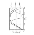
そして、第1の条件乃至第3の条件では、給電装置301の交流電源302から出力される交流電圧の周波数fを、11.56MHzから15.56MHzまで変化させ、給電装置301から受電装置303への無線給電における電力伝送損失を調べた。
In the first to third conditions, the frequency f of the AC voltage output from the
図7に、周波数f(MHz)に対する、電力伝送損失(dB)の測定値を示す。図7において、パターン1で示される実線は、条件1における周波数f(MHz)と電力伝送損失(dB)の関係を示している。パターン2で示される実線は、条件2における周波数f(MHz)と電力伝送損失(dB)の関係を示している。パターン3で示される実線は、条件3における周波数f(MHz)と電力伝送損失(dB)の関係を示している。
FIG. 7 shows measured values of power transmission loss (dB) with respect to frequency f (MHz). In FIG. 7, the solid line indicated by the
図7では、周波数fが13.56MHzである場合に、条件1の電力伝送損失(パターン1で示す実線)と、条件3の電力伝送損失(パターン3で示す実線)とが、ほぼ同等の値を示している。よって、給電装置301から出力される電波が受信可能な範囲内に、整流回路において第2の動作が行われている受電装置304が存在する場合としない場合とで、給電装置301から受電装置303への電力伝送効率は、大きく変わらないことが、証明された。
In FIG. 7, when the frequency f is 13.56 MHz, the power transmission loss of condition 1 (solid line indicated by pattern 1) and the power transmission loss of condition 3 (solid line indicated by pattern 3) are substantially equal values. Is shown. Therefore, the
また、図7では、周波数fが13.56MHzである場合に、条件2の電力伝送損失(パターン2で示す実線)が、他の条件の場合よりも低い値を示している。よって、給電装置301から出力される電波が受信可能な範囲内に、整流回路において第1の動作が行われている受電装置304が存在すると、給電装置301から受電装置303への電力伝送効率が大きく低下することが、証明された。
In FIG. 7, when the frequency f is 13.56 MHz, the power transmission loss of condition 2 (solid line indicated by pattern 2) shows a lower value than in the other conditions. Therefore, when the
本実施の形態は、他の実施の形態と適宜組み合わせて実施することが可能である。 This embodiment can be implemented in appropriate combination with any of the other embodiments.
(実施の形態4)
本実施の形態では、本発明の一態様に係る受電装置100と、給電装置200の、より具体的な構成について説明する。
(Embodiment 4)
In this embodiment, more specific structures of the
図8に、受電装置100の具体的な構成の一例を示す。受電装置100は、共鳴用アンテナ101と、受電用アンテナ102と、整流回路103と、制御回路104と、負荷105と、受信回路106とを有する。
FIG. 8 illustrates an example of a specific configuration of the
共鳴用アンテナ101は、アンテナ素子107と容量素子108とが接続された等価回路で示される。
The
受電用アンテナ102が有する給電点A1及び給電点A2は、整流回路103が有する入力端子B1及び入力端子B2に、それぞれ接続されている。よって、給電点A1の電位は、入力端子B1に与えられ、給電点A2の電位は、入力端子B2に与えられる。
A feeding point A1 and a feeding point A2 included in the
また、整流回路103は、スイッチ110として機能するトランジスタ110tと、スイッチ111として機能するトランジスタ111tとを有する。また、図8において整流回路103は、容量素子112を有する。
The
図8では、スイッチ110として一のトランジスタ110tを用いる場合を例示しているが、スイッチ110として複数のトランジスタを用いても良いし、トランジスタ以外の回路素子を用いても良い。また、図8では、スイッチ111として一のトランジスタ111tを用いる場合を例示しているが、スイッチ111として複数のトランジスタを用いても良いし、トランジスタ以外の回路素子を用いても良い。
Although FIG. 8 illustrates the case where one
トランジスタ110tが有するソース端子またはドレイン端子は、一方が入力端子B1に接続され、他方が出力端子C1に接続されている。トランジスタ111tが有するソース端子またはドレイン端子は、一方が入力端子B2に接続され、他方が出力端子C1に接続されている。
One of a source terminal and a drain terminal of the
なお、トランジスタのソース端子とは、活性層の一部であるソース領域、或いは活性層に接続されたソース電極を意味する。同様に、トランジスタのドレイン端子とは、活性層の一部であるドレイン領域、或いは活性層に接続されたドレイン電極を意味する。 Note that a source terminal of a transistor means a source region that is part of an active layer or a source electrode connected to the active layer. Similarly, the drain terminal of a transistor means a drain region that is part of an active layer or a drain electrode connected to the active layer.
そして、制御回路104は、トランジスタ110tが有するゲート電極への電位の供給と、トランジスタ111tが有するゲート電極への電位の供給とを行う。よって、制御回路104から、トランジスタ110tが有するゲート電極と、トランジスタ111tが有するゲート電極とに与えられる電位に従って、整流回路103は、第1の動作と第2の動作のいずれかを行うことができる。
The
容量素子112が有する一対の電極は、一方が出力端子C1に接続され、他方が出力端子C2に接続されている。また、出力端子C2は、グラウンドなどの基準電位が与えられており、出力端子C1と出力端子C2の電位差は、容量素子112により平滑化される。よって、平滑化された出力端子C1と出力端子C2の電位差が、直流電圧として負荷105に与えられる。
One of the pair of electrodes included in the capacitor 112 is connected to the output terminal C1, and the other is connected to the output terminal C2. The output terminal C2 is given a reference potential such as ground, and the potential difference between the output terminal C1 and the output terminal C2 is smoothed by the capacitor 112. Therefore, the smoothed potential difference between the output terminal C1 and the output terminal C2 is applied to the
次いで、図9に、給電装置200の具体的な構成の一例を示す。給電装置200は、共鳴用アンテナ201と、励振用アンテナ202と、交流電源203と、制御回路204と、送信回路205とを有する。
Next, FIG. 9 illustrates an example of a specific configuration of the
共鳴用アンテナ201は、アンテナ素子206と容量素子207とが接続された等価回路で示される。励振用アンテナ202は、アンテナ素子208と容量素子209とが接続された等価回路で示される。
The
交流電源203は、スイッチとして機能するトランジスタ211t、トランジスタ212t、トランジスタ213t、及びトランジスタ214tと、直流電源215とを有する。トランジスタ211tが有するソース端子またはドレイン端子は、一方に直流電源215からの電圧が与えられ、他方は交流電源203の出力端子D2に接続されている。直流電源215からの電位は、グラウンドなどの基準電位よりも高いものとする。トランジスタ212tが有するソース端子またはドレイン端子は、一方が交流電源203の出力端子D1に接続されており、他方にグラウンドなどの基準電位が与えられている。トランジスタ213tが有するソース端子またはドレイン端子は、一方が交流電源203の出力端子D2に接続されており、他方にグラウンドなどの基準電位が与えられている。トランジスタ214tが有するソース端子またはドレイン端子は、一方に直流電源215からの電位が与えられ、他方は交流電源203の出力端子D1に接続されている。
The
そして、制御回路204は、トランジスタ211t、トランジスタ212t、トランジスタ213t、及びトランジスタ214tがそれぞれ有するゲート電極への、電位の供給を行う。トランジスタ211t、トランジスタ212t、トランジスタ213t、及びトランジスタ214tがそれぞれオンまたはオフになることで、直流電源215からの電位と基準電位とが、交互に出力端子D1と出力端子D2に与えられ、出力端子D1と出力端子D2の間に交流電圧が印加される。そして、当該交流電圧は、励振用アンテナ202に供給される。
The
そして、制御回路204が上記ゲート電極に与える電位を制御することで、交流電源203から励振用アンテナ202に供給される交流電圧の周期が、制御される。
The cycle of the AC voltage supplied from the
次いで、図8に示した受電装置100及び図9に示した給電装置200の動作の一例について、図10に示すタイミングチャートを用いて説明する。ただし、図10では、トランジスタ110t及びトランジスタ111tと、トランジスタ211t乃至トランジスタ214tとが、全てnチャネル型である場合を例に挙げて説明する。
Next, an example of operation of the
受電装置100の整流回路103において第1の動作が行われている場合、図10(A)に示すタイミングチャートに従って、トランジスタ110t及びトランジスタ111tと、トランジスタ211t乃至トランジスタ214tとは、動作を行う。図10(A)では、受電用アンテナ102において、給電点A2における電位を基準としたときの、給電点A1と給電点A2の電位差を、電圧Vpとして示している。
When the first operation is performed in the
図10(A)に示すタイミングチャートに従うと、トランジスタ211t及びトランジスタ212tのゲート電極に与えられる電位がハイレベルである場合に、トランジスタ213t及びトランジスタ214tのゲート電極に与えられる電位がローレベルとなる。すなわち、トランジスタ211t及びトランジスタ212tがオンである場合に、トランジスタ213t及びトランジスタ214tがオフとなる。
According to the timing chart shown in FIG. 10A, when the potentials applied to the gate electrodes of the
上記動作により、出力端子D1に基準電位が与えられ、出力端子D2に直流電源215からの電位が与えられる。よって、出力端子D2における電位を基準としたときの、出力端子D1と出力端子D2の間の電圧は、ローレベルとなる。そして、出力端子D1と出力端子D2の間の電圧が励振用アンテナ202、共鳴用アンテナ201、共鳴用アンテナ101、及び受電用アンテナ102を介して、給電点A1と給電点A2に与えられるため、電圧Vpはローレベルとなる。
Through the above operation, the reference potential is applied to the output terminal D1, and the potential from the
また、図10(A)に示すタイミングチャートに従うと、トランジスタ211t及びトランジスタ212tのゲート電極に与えられる電位がローレベルである場合に、トランジスタ213t及びトランジスタ214tのゲート電極に与えられる電位がハイレベルとなる。すなわち、トランジスタ211t及びトランジスタ212tがオフである場合に、トランジスタ213t及びトランジスタ214tがオンとなる。
Further, according to the timing chart shown in FIG. 10A, when the potentials applied to the gate electrodes of the
上記動作により、出力端子D1に直流電源215からの電位が与えられ、基準電位が出力端子D2に与えられる。よって、出力端子D2における電位を基準としたときの、出力端子D1と出力端子D2の間の電圧は、ハイレベルとなる。そして、出力端子D1と出力端子D2の間の電圧が励振用アンテナ202、共鳴用アンテナ201、共鳴用アンテナ101、及び受電用アンテナ102を介して、給電点A1と給電点A2に与えられるため、電圧Vpはハイレベルとなる。
Through the above operation, the potential from the
そして、図10(A)に示すタイミングチャートに従うと、電圧Vpがローレベルの場合、すなわち、給電点A2の電位が給電点A1の電位よりも高い場合に、トランジスタ110tのゲート電極に与えられる電位がローレベル、トランジスタ111tのゲート電極に与えられる電位がハイレベルとなる。すなわち、トランジスタ110tはオフ、トランジスタ111tはオンとなる。よって、より高い電位である給電点A2の電位が、トランジスタ111tを介して出力端子C1に与えられる。
Then, according to the timing chart shown in FIG. 10A, when the voltage Vp is at a low level, that is, when the potential at the feeding point A2 is higher than the potential at the feeding point A1, the potential applied to the gate electrode of the
また、図10(A)に示すタイミングチャートに従うと、電圧Vpがハイレベルの場合、すなわち、給電点A1の電位が給電点A2の電位よりも高い場合に、トランジスタ110tのゲート電極に与えられる電位がハイレベル、トランジスタ111tのゲート電極に与えられる電位がローレベルとなる。すなわち、トランジスタ110tはオン、トランジスタ111tはオフとなる。よって、より高い電位である給電点A1の電位が、トランジスタ110tを介して出力端子C1に与えられる。
Further, according to the timing chart shown in FIG. 10A, when the voltage Vp is at a high level, that is, when the potential at the feeding point A1 is higher than the potential at the feeding point A2, the potential applied to the gate electrode of the
上記第1の動作により、出力端子C1には出力端子C2よりも高い電位が与えられる。すなわち、上記第1の動作により、給電点A1と給電点A2の間に印加される交流の電圧Vpが整流され、出力端子C1及び出力端子C2間に印加されることとなる。出力端子C1及び出力端子C2間に印加された直流電圧は、負荷105に供給される。
By the first operation, a higher potential than the output terminal C2 is applied to the output terminal C1. That is, by the first operation, the AC voltage Vp applied between the feeding point A1 and the feeding point A2 is rectified and applied between the output terminal C1 and the output terminal C2. The DC voltage applied between the output terminal C1 and the output terminal C2 is supplied to the
上記第1の動作において、トランジスタ110t及びトランジスタ111tのオンとオフの切り替えのタイミングは、給電装置200の交流電源203において出力される交流電圧の周期に従って、制御回路104において定めることができる。
In the first operation, the timing for switching on and off of the
また、受電装置100の整流回路103において第2の動作が行われている場合、図10(B)に示すタイミングチャートに従って、トランジスタ110t及びトランジスタ111tと、トランジスタ211t乃至トランジスタ214tとは、動作を行う。図10(B)でも、受電用アンテナ102において、給電点A2における電位を基準としたときの、給電点A1と給電点A2の電位差を、電圧Vpとして示している。
In addition, when the second operation is performed in the
第1の動作の場合と第2の動作の場合とで、給電装置200におけるトランジスタ211t乃至トランジスタ214tの動作は、同じである。よって、図10(B)に示すタイミングチャートに従い、トランジスタ211t乃至トランジスタ214tが動作を行うことで、出力端子D1と出力端子D2の間に、ローレベルの電圧とハイレベルの電圧とが交互に与えられる。
The operation of the
そして、図10(B)に示すタイミングチャートに従うと、トランジスタ110t及びトランジスタ111tのゲート電極に与えられる電位は、連続してハイレベルである。すなわち、トランジスタ110t及びトランジスタ111tは連続してオンとなる。よって、給電点A1と給電点A2は短絡されるので、電圧Vpは0にほぼ等しくなる。そして、出力端子D1と出力端子D2の間にローレベルの電圧とハイレベルの電圧とが交互に与えられていても、受電用アンテナ102に接続された回路素子や配線、具体的には、整流回路103が有する容量素子112、負荷105を構成する回路素子、整流回路103や負荷105に設けられた配線などへの、電力の供給は停止される。そのため、受電装置100の共鳴用アンテナ101は、給電装置200の共鳴用アンテナ201から電力を実質的に受け取らなくなる。
Then, according to the timing chart shown in FIG. 10B, the potentials applied to the gate electrodes of the
したがって、本発明の一態様では、受電装置100において、共鳴用アンテナ101が有するアンテナ素子107の一対の給電点を短絡させなくとも、給電装置200からの電力の供給を停止することができる。そして、給電装置200から、充電の完了した受電装置100への電力の供給が停止されることで、給電装置200から他の受電装置への電力伝送効率を高めることができる。
Therefore, in one embodiment of the present invention, in the
なお、図8に示す受電装置100及び図9に示す給電装置200では、図1に示す無線給電システムのように、受信回路106が、電力の供給を行うためのアンテナ群を介して、送信回路205から、周期を情報として含む信号を受け取る形態を有していても良い。或いは、図8に示す受電装置100及び図9に示す給電装置200では、図2に示す無線給電システムのように、受信回路106が、電力の供給を行うためのアンテナ群とは異なるアンテナ群を介して、送信回路205から、周期を情報として含む信号を受け取る形態を有していても良い。或いは、一部のアンテナが、電力の供給を行うためのアンテナ群と、信号の授受を行うためのアンテナ群の両方に、属していても良い。
Note that, in the
本実施の形態は、他の実施の形態と適宜組み合わせて実施することが可能である。 This embodiment can be implemented in appropriate combination with any of the other embodiments.
(実施の形態5)
本発明の一態様に係る受電装置は、外部からの電力の供給を無線で受けられる電子機器である。本発明の一態様に係る受電装置の具体例として、表示装置、ノート型パーソナルコンピュータ、記録媒体を備えた画像再生装置(代表的にはDVD:Digital Versatile Disc等の記録媒体を再生し、その画像を表示しうるディスプレイを有する装置)、携帯電話、携帯型ゲーム機、携帯情報端末、電子書籍、ビデオカメラ、デジタルスチルカメラなどのカメラ、ゴーグル型ディスプレイ(ヘッドマウントディスプレイ)、ナビゲーションシステム、音響再生装置(カーオーディオ、デジタルオーディオプレイヤー等)、複写機、ファクシミリ、プリンター、プリンター複合機、現金自動預け入れ払い機(ATM)、自動販売機などが挙げられる。
(Embodiment 5)
A power receiving device according to one embodiment of the present invention is an electronic device that can receive power from the outside wirelessly. Specific examples of a power receiving device according to one embodiment of the present invention include a display device, a notebook personal computer, and an image reproducing device including a recording medium (typically, a recording medium such as a DVD: Digital Versatile Disc). Device having a display capable of displaying a mobile phone, a portable game machine, a portable information terminal, a camera such as an electronic book, a video camera, a digital still camera, a goggle-type display (head-mounted display), a navigation system, and a sound reproducing device. (Car audio, digital audio player, etc.), copier, facsimile, printer, printer multifunction device, automatic teller machine (ATM), vending machine, and the like.
また、本発明の一態様に係る受電装置は、電力を用いて電動機により推進する移動体であっても良い。上記移動体には、自動車(自動二輪車、三輪以上の普通自動車)、電動アシスト自転車を含む原動機付自転車、航空機、船舶、鉄道車両などが、その範疇に含まれる。 Further, the power receiving device according to one embodiment of the present invention may be a moving body that is propelled by an electric motor using electric power. Examples of the moving body include automobiles (motorcycles, ordinary automobiles of three or more wheels), motorbikes including electric assist bicycles, airplanes, ships, and railway vehicles.
本実施の形態では、外部からの電力の供給を無線で受けられる複数の移動体に、給電装置から無線給電を行う場合について説明する。 In this embodiment, a case will be described in which wireless power feeding is performed from a power feeding device to a plurality of moving bodies that can receive power from the outside wirelessly.
まず、図11(A)に示すように、電磁共鳴方式を用いた無線給電により、給電装置500から、普通自動車501、普通自動車502、及び電動車いす503に電力を供給する。普通自動車501、普通自動車502、及び電動車いす503には、それぞれ負荷として蓄電装置及び充電制御回路が設けられている。給電装置500から供給された電力の一部は、普通自動車501、普通自動車502、及び電動車いす503がそれぞれ有する蓄電装置に蓄えられる。
First, as illustrated in FIG. 11A, electric power is supplied from the
図11(A)に示すように、無線給電による電力の供給が行われている間、普通自動車501、普通自動車502、及び電動車いす503が有する整流回路は、第1の動作を行う。
As illustrated in FIG. 11A, the rectifier circuit included in the
そして、例えば、電動車いす503が有する蓄電装置が満充電になると、電動車いす503が有する整流回路の動作は、充電制御回路からの信号に従って、第1の動作から第2の動作に切り換わる。そして、給電装置500から充電の完了した電動車いす503への、電力の供給が停止することで、給電装置500から普通自動車501及び普通自動車502への電力伝送効率が高まる(図11(B)参照)。
For example, when the power storage device included in the
本実施の形態は、他の実施の形態と適宜組み合わせて実施することが可能である。 This embodiment can be implemented in appropriate combination with any of the other embodiments.
100 受電装置
101 共鳴用アンテナ
102 受電用アンテナ
103 整流回路
104 制御回路
105 負荷
106 受信回路
107 アンテナ素子
108 容量素子
109 アンテナ素子
110 スイッチ
110t トランジスタ
111 スイッチ
111t トランジスタ
112 容量素子
113 アンテナ
114 蓄電装置
115 充電制御回路
200 給電装置
201 共鳴用アンテナ
202 励振用アンテナ
203 交流電源
204 制御回路
205 送信回路
206 アンテナ素子
207 容量素子
208 アンテナ素子
209 容量素子
210 アンテナ
211t トランジスタ
212t トランジスタ
213t トランジスタ
214t トランジスタ
215 直流電源
301 給電装置
302 交流電源
303 受電装置
304 受電装置
500 給電装置
501 普通自動車
502 普通自動車
DESCRIPTION OF
Claims (4)
前記第1アンテナとの間で電磁誘導による結合を形成する機能を有する第2アンテナと、
前記第1アンテナ及び前記第2アンテナを介して前記給電装置から与えられる交流電圧を整流して直流電圧を生成する第1の機能と、前記第2アンテナが有するアンテナ素子の一対の給電点を短絡させる第2の機能と、を有する整流回路と、
前記交流電圧から周期の情報を含む第1信号を抽出する機能を有する受信回路と、
制御回路と、を有し、
前記制御回路は、前記整流回路における前記第1の機能と前記第2の機能とを選択する機能を有し、
前記制御回路は、前記第1の機能が選択されている間、前記整流回路が有する複数のスイッチを制御するための第2信号を前記第1信号に従って生成する機能を有する受電装置。 A first antenna having a function of forming a resonance coupling with the antenna of the power feeding device;
A second antenna having a function of forming a coupling by electromagnetic induction with the first antenna;
A first function of rectifying an AC voltage supplied from the power feeding device via the first antenna and the second antenna to generate a DC voltage, and a pair of feeding points of antenna elements of the second antenna are short-circuited. A rectifier circuit having a second function of:
A receiving circuit having a function of extracting a first signal including period information from the AC voltage;
A control circuit,
The control circuit has a function of selecting the first function and the second function in the rectifier circuit;
The control circuit has a function of generating a second signal for controlling a plurality of switches included in the rectifier circuit according to the first signal while the first function is selected.
前記第1アンテナとの間で電磁誘導による結合を形成する機能を有する第2アンテナと、
前記給電装置からの電波を受信して第2の交流電圧を生成する機能を有する第3のアンテナと、
前記第1アンテナ及び前記第2アンテナを介して前記給電装置から与えられる交流電圧を整流して直流電圧を生成する第1の機能と、前記第2アンテナが有するアンテナ素子の一対の給電点を短絡させる第2の機能と、を有する整流回路と、
前記第2の交流電圧から周期の情報を含む第1信号を抽出する機能を有する受信回路と、
制御回路と、を有し、
前記制御回路は、前記整流回路における前記第1の機能と前記第2の機能とを選択する機能を有し、
前記制御回路は、前記第1の機能が選択されている間、前記整流回路が有する複数のスイッチを制御するための第2信号を前記第1信号に従って生成する機能を有する受電装置。 A first antenna having a function of forming a resonance coupling with the antenna of the power feeding device;
A second antenna having a function of forming a coupling by electromagnetic induction with the first antenna;
A third antenna having a function of receiving a radio wave from the power feeding device and generating a second AC voltage;
A first function of rectifying an AC voltage supplied from the power feeding device via the first antenna and the second antenna to generate a DC voltage, and a pair of feeding points of antenna elements of the second antenna are short-circuited. A rectifier circuit having a second function of:
A receiving circuit having a function of extracting a first signal including period information from the second AC voltage;
A control circuit,
The control circuit has a function of selecting the first function and the second function in the rectifier circuit;
The control circuit has a function of generating a second signal for controlling a plurality of switches included in the rectifier circuit according to the first signal while the first function is selected.
受電装置と、を有し、
前記受電装置は、前記給電装置が有するアンテナとの間で共鳴による結合を形成する機能を有する第1アンテナと、
前記第1アンテナとの間で電磁誘導による結合を形成する機能を有する第2アンテナと、
前記第1アンテナ及び前記第2アンテナを介して前記給電装置から与えられる交流電圧を整流して直流電圧を生成する第1の機能と、前記第2アンテナが有するアンテナ素子の一対の給電点を短絡させる第2の機能と、を有する整流回路と、
前記交流電圧から周期の情報を含む第1信号を抽出する機能を有する受信回路と、
制御回路と、を有し、
前記制御回路は、前記整流回路における前記第1の機能と前記第2の機能とを選択する機能を有し、
前記制御回路は、前記第1の機能が選択されている間、前記整流回路が有する複数のスイッチを制御するための第2信号を前記第1信号に従って生成する機能を有する無線給電システム。 A power supply device;
A power receiving device,
The power receiving device includes a first antenna having a function of forming a resonance coupling with an antenna of the power feeding device;
A second antenna having a function of forming a coupling by electromagnetic induction with the first antenna;
A first function of rectifying an AC voltage supplied from the power feeding device via the first antenna and the second antenna to generate a DC voltage, and a pair of feeding points of antenna elements of the second antenna are short-circuited. A rectifier circuit having a second function of:
A receiving circuit having a function of extracting a first signal including period information from the AC voltage;
A control circuit,
The control circuit has a function of selecting the first function and the second function in the rectifier circuit;
The wireless power feeding system, wherein the control circuit has a function of generating, according to the first signal, a second signal for controlling a plurality of switches included in the rectifier circuit while the first function is selected.
受電装置と、を有し、
前記受電装置は、前記給電装置が有するアンテナとの間で共鳴による結合を形成する機能を有する第1アンテナと、
前記第1アンテナとの間で電磁誘導による結合を形成する機能を有する第2アンテナと、
前記給電装置からの電波を受信して第2の交流電圧を生成する機能を有する第3のアンテナと、
前記第1アンテナ及び前記第2アンテナを介して前記給電装置から与えられる交流電圧を整流して直流電圧を生成する第1の機能と、前記第2アンテナが有するアンテナ素子の一対の給電点を短絡させる第2の機能と、を有する整流回路と、
前記第2の交流電圧から周期の情報を含む第1信号を抽出する機能を有する受信回路と、
制御回路と、を有し、
前記制御回路は、前記整流回路における前記第1の機能と前記第2の機能とを選択する機能を有し、
前記制御回路は、前記第1の機能が選択されている間、前記整流回路が有する複数のスイッチを制御するための第2信号を前記第1信号に従って生成する機能を有する無線給電システム。 A power supply device;
A power receiving device,
The power receiving device includes a first antenna having a function of forming a resonance coupling with an antenna of the power feeding device;
A second antenna having a function of forming a coupling by electromagnetic induction with the first antenna;
A third antenna having a function of receiving a radio wave from the power feeding device and generating a second AC voltage;
A first function of rectifying an AC voltage supplied from the power feeding device via the first antenna and the second antenna to generate a DC voltage, and a pair of feeding points of antenna elements of the second antenna are short-circuited. A rectifier circuit having a second function of:
A receiving circuit having a function of extracting a first signal including period information from the second AC voltage;
A control circuit,
The control circuit has a function of selecting the first function and the second function in the rectifier circuit;
The wireless power feeding system, wherein the control circuit has a function of generating, according to the first signal, a second signal for controlling a plurality of switches included in the rectifier circuit while the first function is selected.
Priority Applications (1)
| Application Number | Priority Date | Filing Date | Title |
|---|---|---|---|
| JP2012273214A JP6088234B2 (en) | 2011-12-23 | 2012-12-14 | Power receiving device, wireless power feeding system |
Applications Claiming Priority (3)
| Application Number | Priority Date | Filing Date | Title |
|---|---|---|---|
| JP2011282434 | 2011-12-23 | ||
| JP2011282434 | 2011-12-23 | ||
| JP2012273214A JP6088234B2 (en) | 2011-12-23 | 2012-12-14 | Power receiving device, wireless power feeding system |
Related Child Applications (1)
| Application Number | Title | Priority Date | Filing Date |
|---|---|---|---|
| JP2017018683A Division JP6285585B2 (en) | 2011-12-23 | 2017-02-03 | Power receiving apparatus and wireless power feeding system |
Publications (3)
| Publication Number | Publication Date |
|---|---|
| JP2013150542A JP2013150542A (en) | 2013-08-01 |
| JP2013150542A5 JP2013150542A5 (en) | 2016-01-21 |
| JP6088234B2 true JP6088234B2 (en) | 2017-03-01 |
Family
ID=48653861
Family Applications (6)
| Application Number | Title | Priority Date | Filing Date |
|---|---|---|---|
| JP2012273214A Active JP6088234B2 (en) | 2011-12-23 | 2012-12-14 | Power receiving device, wireless power feeding system |
| JP2017018683A Active JP6285585B2 (en) | 2011-12-23 | 2017-02-03 | Power receiving apparatus and wireless power feeding system |
| JP2017212616A Withdrawn JP2018027015A (en) | 2011-12-23 | 2017-11-02 | Power reception device |
| JP2019087010A Withdrawn JP2019162028A (en) | 2011-12-23 | 2019-04-29 | Power reception device |
| JP2019087011A Active JP6715989B2 (en) | 2011-12-23 | 2019-04-29 | Power receiving device |
| JP2021033195A Withdrawn JP2021093910A (en) | 2011-12-23 | 2021-03-03 | Power reception device |
Family Applications After (5)
| Application Number | Title | Priority Date | Filing Date |
|---|---|---|---|
| JP2017018683A Active JP6285585B2 (en) | 2011-12-23 | 2017-02-03 | Power receiving apparatus and wireless power feeding system |
| JP2017212616A Withdrawn JP2018027015A (en) | 2011-12-23 | 2017-11-02 | Power reception device |
| JP2019087010A Withdrawn JP2019162028A (en) | 2011-12-23 | 2019-04-29 | Power reception device |
| JP2019087011A Active JP6715989B2 (en) | 2011-12-23 | 2019-04-29 | Power receiving device |
| JP2021033195A Withdrawn JP2021093910A (en) | 2011-12-23 | 2021-03-03 | Power reception device |
Country Status (2)
| Country | Link |
|---|---|
| US (2) | US9231429B2 (en) |
| JP (6) | JP6088234B2 (en) |
Families Citing this family (29)
| Publication number | Priority date | Publication date | Assignee | Title |
|---|---|---|---|---|
| US9246357B2 (en) * | 2011-12-07 | 2016-01-26 | Semiconductor Energy Laboratory Co., Ltd. | Contactless power feeding system |
| JP6088234B2 (en) * | 2011-12-23 | 2017-03-01 | 株式会社半導体エネルギー研究所 | Power receiving device, wireless power feeding system |
| US9673867B2 (en) | 2012-03-14 | 2017-06-06 | Semiconductor Energy Laboratory Co., Ltd. | Power transmission device and power feeding system |
| FR2996372B1 (en) * | 2012-10-01 | 2015-05-15 | Renault Sa | NON-CONTACT CHARGING SYSTEM OF A MOTOR VEHICLE BATTERY |
| US9414309B2 (en) * | 2012-11-16 | 2016-08-09 | Intel Deutschland Gmbh | Mobile terminal |
| KR20140097628A (en) * | 2013-01-28 | 2014-08-07 | 삼성에스디아이 주식회사 | temperature controlling system of battery and controlling method thereof |
| TWI482389B (en) * | 2013-03-01 | 2015-04-21 | Luxx Lighting Technology Taiwan Ltd | Inductive power transfer system, and transmitter and receiver devices thereof |
| TWI486788B (en) * | 2013-04-03 | 2015-06-01 | Univ Nat Taiwan | Transmission interface device and system thereof |
| JP2014204348A (en) * | 2013-04-05 | 2014-10-27 | 帝人株式会社 | Antenna device |
| JP5939314B2 (en) * | 2013-06-05 | 2016-06-22 | 株式会社村田製作所 | Electronic device and wireless power transmission system |
| JP5832672B2 (en) * | 2013-10-31 | 2015-12-16 | 三菱電機エンジニアリング株式会社 | Resonant type high frequency power supply |
| CN103633748B (en) * | 2013-11-12 | 2015-09-09 | 天津工业大学 | Electromagnetic resonance type railway locomotive wireless power supply system |
| JP6188820B2 (en) * | 2013-12-10 | 2017-08-30 | 三菱電機エンジニアリング株式会社 | Rectifier circuit for high frequency power supply |
| WO2015118945A1 (en) * | 2014-02-07 | 2015-08-13 | 株式会社村田製作所 | Power transmission system |
| CN104882973B (en) * | 2014-02-28 | 2017-10-27 | 广东美的生活电器制造有限公司 | Combined electrical apparatus system |
| JP6172088B2 (en) * | 2014-08-19 | 2017-08-02 | 株式会社デンソー | Resonant current limiter |
| JP6179730B2 (en) * | 2014-09-19 | 2017-08-16 | パナソニックIpマネジメント株式会社 | Power receiving device, non-contact power transmission system, and charging method |
| GB2531379A (en) * | 2014-10-10 | 2016-04-20 | Zwipe As | Power load management |
| US20160118805A1 (en) * | 2014-10-24 | 2016-04-28 | Motorola Solutions, Inc | Wireless power transfer system and method thereof |
| US10250804B2 (en) | 2015-04-07 | 2019-04-02 | Vivint, Inc. | Induction-powered camera |
| WO2017123190A1 (en) * | 2016-01-11 | 2017-07-20 | Daramic, Llc | Improved battery separators for e-rickshaw and similar vehicle lead acid batteries |
| SG10201700633QA (en) * | 2016-02-03 | 2017-09-28 | Gen Electric | System and method for protecting a wireless power transfer system |
| US10954911B2 (en) * | 2016-10-19 | 2021-03-23 | Walbro Llc | Control and communication module for light-duty combustion engine |
| GB2558672B (en) * | 2017-01-17 | 2022-02-02 | Stannah Stairlifts Ltd | Improvements in or relating to stairlifts |
| TWI674727B (en) * | 2018-07-12 | 2019-10-11 | 鑫東龍安防股份有限公司 | Wireless energy acquisition device and power supply control method thereof |
| GB2575685B (en) * | 2018-07-20 | 2020-11-18 | Drayson Tech Europe Ltd | Circuitry for use in smart cards and other applications |
| KR20200054614A (en) * | 2018-11-12 | 2020-05-20 | 삼성전자주식회사 | Accessory device |
| CN112509782B (en) * | 2020-11-27 | 2022-07-01 | 兰州空间技术物理研究所 | Electromagnetic lock working power reduction circuit |
| CN115693979A (en) * | 2021-07-22 | 2023-02-03 | 北京小米移动软件有限公司 | Wireless charging receiving circuit and method, electronic equipment and wireless charging system |
Family Cites Families (69)
| Publication number | Priority date | Publication date | Assignee | Title |
|---|---|---|---|---|
| NL8901659A (en) | 1989-06-30 | 1991-01-16 | Nedap Nv | MULTIPASS SYSTEM. |
| JP2803943B2 (en) | 1992-10-21 | 1998-09-24 | アルプス電気株式会社 | Non-contact power supply |
| US5790946A (en) | 1993-07-15 | 1998-08-04 | Rotzoll; Robert R. | Wake up device for a communications system |
| JPH1127870A (en) * | 1997-07-03 | 1999-01-29 | Toyota Autom Loom Works Ltd | Charge method, charging equipment, charger, and vehicle |
| US6837438B1 (en) | 1998-10-30 | 2005-01-04 | Hitachi Maxell, Ltd. | Non-contact information medium and communication system utilizing the same |
| US6509217B1 (en) | 1999-10-22 | 2003-01-21 | Damoder Reddy | Inexpensive, reliable, planar RFID tag structure and method for making same |
| US20020049714A1 (en) | 2000-05-11 | 2002-04-25 | Shunpei Yamazaki | Communication system |
| JP4200257B2 (en) | 2000-09-26 | 2008-12-24 | パナソニック電工株式会社 | Non-contact power transmission device |
| US7209771B2 (en) | 2000-12-22 | 2007-04-24 | Terahop Networks, Inc. | Battery powered wireless transceiver having LPRF component and second wake up receiver |
| US6850080B2 (en) | 2001-03-19 | 2005-02-01 | Semiconductor Energy Laboratory Co., Ltd. | Inspection method and inspection apparatus |
| SG142160A1 (en) | 2001-03-19 | 2008-05-28 | Semiconductor Energy Lab | Method of manufacturing a semiconductor device |
| US6944424B2 (en) | 2001-07-23 | 2005-09-13 | Intermec Ip Corp. | RFID tag having combined battery and passive power source |
| US6737302B2 (en) | 2001-10-31 | 2004-05-18 | Semiconductor Energy Laboratory Co., Ltd. | Manufacturing method for field-effect transistor |
| US7215976B2 (en) | 2001-11-30 | 2007-05-08 | Symbol Technologies, Inc. | RFID device, system and method of operation including a hybrid backscatter-based RFID tag protocol compatible with RFID, bluetooth and/or IEEE 802.11x infrastructure |
| JP3866594B2 (en) | 2002-03-15 | 2007-01-10 | Necエレクトロニクス株式会社 | Delay circuit, semiconductor memory device, and control method of semiconductor memory device |
| WO2004036482A2 (en) | 2002-10-18 | 2004-04-29 | Symbol Technologies, Inc. | System and method for minimizing unwanted re-negotiation of a passive rfid tag |
| US7072697B2 (en) | 2002-10-22 | 2006-07-04 | Nokia Corporation | Method and device for transponder aided wake-up of a low power radio device by a wake-up event |
| US7652359B2 (en) | 2002-12-27 | 2010-01-26 | Semiconductor Energy Laboratory Co., Ltd. | Article having display device |
| US7603144B2 (en) | 2003-01-02 | 2009-10-13 | Cymbet Corporation | Active wireless tagging system on peel and stick substrate |
| JP2005235615A (en) | 2004-02-20 | 2005-09-02 | Hitachi Maxell Ltd | Adapter panel, electronic equipment and cable connector recognition system |
| JP4611093B2 (en) | 2004-05-12 | 2011-01-12 | セイコーインスツル株式会社 | Radio power generation circuit |
| KR20070067675A (en) | 2004-07-01 | 2007-06-28 | 파워아이디 리미티드 | Battery-assisted backscatter rfid transponder |
| JP2006024087A (en) | 2004-07-09 | 2006-01-26 | Nec Corp | Radio device, its manufacturing method, its inspecting method and inspecting device, radio apparatus, and its manufacturing method |
| US8045947B2 (en) * | 2004-09-17 | 2011-10-25 | Massachusetts Institute Of Technology | RF power extracting circuit and related techniques |
| US20060103533A1 (en) | 2004-11-15 | 2006-05-18 | Kourosh Pahlavan | Radio frequency tag and reader with asymmetric communication bandwidth |
| JP2006180073A (en) | 2004-12-21 | 2006-07-06 | Okayama Prefecture | Wireless ic tag |
| JP4677859B2 (en) * | 2005-08-25 | 2011-04-27 | 東芝ライテック株式会社 | LED lighting device |
| CN101401112B (en) | 2006-03-10 | 2013-01-02 | 株式会社半导体能源研究所 | Semiconductor device |
| CN101395617B (en) | 2006-03-10 | 2012-05-30 | 株式会社半导体能源研究所 | Semiconductor device and method for operating the same |
| WO2007108371A1 (en) | 2006-03-15 | 2007-09-27 | Semiconductor Energy Laboratory Co., Ltd. | Semiconductor device |
| KR101433306B1 (en) | 2006-03-15 | 2014-08-22 | 가부시키가이샤 한도오따이 에네루기 켄큐쇼 | Electric power supply system and electric power supply system for motor vehicle |
| EP2002383B1 (en) | 2006-03-15 | 2012-04-25 | Semiconductor Energy Laboratory Co., Ltd. | Semiconductor device |
| KR101435966B1 (en) | 2006-05-31 | 2014-08-29 | 가부시키가이샤 한도오따이 에네루기 켄큐쇼 | Semiconductor device and ic label, ic tag, and ic card having the same |
| US8132026B2 (en) | 2006-06-02 | 2012-03-06 | Semiconductor Energy Laboratory Co., Ltd. | Power storage device and mobile electronic device having the same |
| JP2008035637A (en) * | 2006-07-28 | 2008-02-14 | Kokusan Denki Co Ltd | Battery charge control device |
| EP1895450B1 (en) | 2006-08-31 | 2014-03-05 | Semiconductor Energy Laboratory Co., Ltd. | Semiconductor device and power receiving device |
| US20090160261A1 (en) | 2007-12-19 | 2009-06-25 | Nokia Corporation | Wireless energy transfer |
| JP4544339B2 (en) * | 2008-04-28 | 2010-09-15 | ソニー株式会社 | Power transmission device, power transmission method, program, and power transmission system |
| US8278784B2 (en) * | 2008-07-28 | 2012-10-02 | Qualcomm Incorporated | Wireless power transmission for electronic devices |
| US8947041B2 (en) * | 2008-09-02 | 2015-02-03 | Qualcomm Incorporated | Bidirectional wireless power transmission |
| JP5258521B2 (en) | 2008-11-14 | 2013-08-07 | トヨタ自動車株式会社 | Power supply system |
| JP4759610B2 (en) | 2008-12-01 | 2011-08-31 | 株式会社豊田自動織機 | Non-contact power transmission device |
| JP2010193598A (en) | 2009-02-17 | 2010-09-02 | Nippon Soken Inc | Noncontact power supply facility and noncontact power supply system |
| JP5365276B2 (en) | 2009-03-17 | 2013-12-11 | ソニー株式会社 | Power transmission system and power output device |
| DK2409548T3 (en) * | 2009-03-19 | 2018-05-22 | Greengage Lighting Ltd | ELECTRICAL SYSTEM FOR HIGH FREQUENCY AC AND WITH INACTIVATELY CONNECTED LOADS AND SIMILAR POWER SUPPLIES AND LIGHTING FITTINGS |
| JP2010226890A (en) * | 2009-03-24 | 2010-10-07 | Panasonic Electric Works Co Ltd | Non-contact power transmission apparatus |
| JP5621203B2 (en) | 2009-03-30 | 2014-11-12 | 富士通株式会社 | Wireless power supply system and wireless power supply method |
| JP5365306B2 (en) | 2009-03-31 | 2013-12-11 | 富士通株式会社 | Wireless power supply system |
| JP4865001B2 (en) | 2009-04-13 | 2012-02-01 | 株式会社日本自動車部品総合研究所 | Non-contact power supply equipment, non-contact power receiving device and non-contact power supply system |
| JP2010252468A (en) | 2009-04-14 | 2010-11-04 | Sony Corp | Power transmission device and method, power receiving device and method, and power transmission system |
| JP5499534B2 (en) * | 2009-07-07 | 2014-05-21 | ソニー株式会社 | Non-contact power receiving apparatus, power receiving method in non-contact power receiving apparatus, and non-contact power feeding system |
| JP2011029799A (en) | 2009-07-23 | 2011-02-10 | Sony Corp | Contactless power supplying communication apparatus, contactless power receiving communication device, power-supplying communication control method, and power receiving communication control method |
| JP5499955B2 (en) | 2009-10-05 | 2014-05-21 | Tdk株式会社 | Wireless power supply apparatus and wireless power transmission system |
| JP5664019B2 (en) | 2009-10-28 | 2015-02-04 | Tdk株式会社 | Wireless power feeder, wireless power transmission system, and table and table lamp using the same |
| JP5664018B2 (en) | 2009-10-30 | 2015-02-04 | Tdk株式会社 | Wireless power feeder, wireless power transmission system, and table and table lamp using the same |
| JP2011114985A (en) * | 2009-11-27 | 2011-06-09 | Sanyo Electric Co Ltd | Apparatus with built-in battery and charging pad |
| US8410637B2 (en) * | 2009-11-30 | 2013-04-02 | Broadcom Corporation | Wireless power system with selectable control channel protocols |
| JP2011182506A (en) * | 2010-02-26 | 2011-09-15 | Mitsuba Corp | Electric motor, and motor device |
| CN102823109B (en) * | 2010-04-13 | 2015-01-28 | 富士通株式会社 | Power supply system, power transmitter, and power receiver |
| JP5139469B2 (en) | 2010-04-27 | 2013-02-06 | 株式会社日本自動車部品総合研究所 | Coil unit and wireless power supply system |
| US20110285211A1 (en) | 2010-05-20 | 2011-11-24 | Advantest Corporation | Wireless power supply system |
| KR101854420B1 (en) | 2010-11-26 | 2018-05-03 | 가부시키가이샤 한도오따이 에네루기 켄큐쇼 | Power transmission device and wireless power transmission system including the same |
| US9054544B2 (en) | 2010-12-22 | 2015-06-09 | Semiconductor Energy Laboratory Co., Ltd. | Power feeding device, power receiving device, and wireless power feed system |
| JP2013078171A (en) | 2011-09-29 | 2013-04-25 | Semiconductor Energy Lab Co Ltd | Power receiving device and non-contact power supply system |
| US9502920B2 (en) | 2011-11-16 | 2016-11-22 | Semiconductor Energy Laboratory Co., Ltd. | Power receiving device, power transmission device, and power feeding system |
| US9246357B2 (en) | 2011-12-07 | 2016-01-26 | Semiconductor Energy Laboratory Co., Ltd. | Contactless power feeding system |
| TWI566508B (en) | 2011-12-16 | 2017-01-11 | 半導體能源研究所股份有限公司 | Dc-dc converter, power receiving device, and power feeding system |
| US9847675B2 (en) | 2011-12-16 | 2017-12-19 | Semiconductor Energy Laboratory Co., Ltd. | Power receiving device and power feeding system |
| JP6088234B2 (en) * | 2011-12-23 | 2017-03-01 | 株式会社半導体エネルギー研究所 | Power receiving device, wireless power feeding system |
-
2012
- 2012-12-14 JP JP2012273214A patent/JP6088234B2/en active Active
- 2012-12-21 US US13/723,491 patent/US9231429B2/en not_active Expired - Fee Related
-
2015
- 2015-12-29 US US14/982,331 patent/US10020670B2/en not_active Expired - Fee Related
-
2017
- 2017-02-03 JP JP2017018683A patent/JP6285585B2/en active Active
- 2017-11-02 JP JP2017212616A patent/JP2018027015A/en not_active Withdrawn
-
2019
- 2019-04-29 JP JP2019087010A patent/JP2019162028A/en not_active Withdrawn
- 2019-04-29 JP JP2019087011A patent/JP6715989B2/en active Active
-
2021
- 2021-03-03 JP JP2021033195A patent/JP2021093910A/en not_active Withdrawn
Also Published As
| Publication number | Publication date |
|---|---|
| JP2018027015A (en) | 2018-02-15 |
| US20160111896A1 (en) | 2016-04-21 |
| US10020670B2 (en) | 2018-07-10 |
| JP2017099285A (en) | 2017-06-01 |
| US20130162203A1 (en) | 2013-06-27 |
| JP2013150542A (en) | 2013-08-01 |
| JP2019162029A (en) | 2019-09-19 |
| JP6285585B2 (en) | 2018-02-28 |
| US9231429B2 (en) | 2016-01-05 |
| JP2019162028A (en) | 2019-09-19 |
| JP6715989B2 (en) | 2020-07-01 |
| JP2021093910A (en) | 2021-06-17 |
Similar Documents
| Publication | Publication Date | Title |
|---|---|---|
| JP6285585B2 (en) | Power receiving apparatus and wireless power feeding system | |
| US11843259B2 (en) | Power feeding device, power receiving device, and wireless power feed system | |
| JP6559761B2 (en) | Contactless power supply system | |
| KR101391487B1 (en) | Power receiving device and power receiving method | |
| JP6053297B2 (en) | Power receiving device, wireless power feeding system | |
| US10014725B2 (en) | Hybrid wireless power transmitting system and method therefor | |
| JP5804052B2 (en) | Wireless power receiving and receiving device and wireless power transmission system | |
| US11296556B2 (en) | Power relay device and system | |
| WO2015035924A1 (en) | Wireless charging device and mobile terminal using same | |
| JP2010284066A (en) | Communication device, communication terminal and communication system | |
| JP6310846B2 (en) | Non-contact power transmission system and secondary battery pack | |
| CN102651568A (en) | Wireless charging device |
Legal Events
| Date | Code | Title | Description |
|---|---|---|---|
| A521 | Request for written amendment filed |
Free format text: JAPANESE INTERMEDIATE CODE: A523 Effective date: 20151201 |
|
| A621 | Written request for application examination |
Free format text: JAPANESE INTERMEDIATE CODE: A621 Effective date: 20151201 |
|
| A977 | Report on retrieval |
Free format text: JAPANESE INTERMEDIATE CODE: A971007 Effective date: 20160822 |
|
| A131 | Notification of reasons for refusal |
Free format text: JAPANESE INTERMEDIATE CODE: A131 Effective date: 20160830 |
|
| A521 | Request for written amendment filed |
Free format text: JAPANESE INTERMEDIATE CODE: A523 Effective date: 20161005 |
|
| A131 | Notification of reasons for refusal |
Free format text: JAPANESE INTERMEDIATE CODE: A131 Effective date: 20161129 |
|
| A521 | Request for written amendment filed |
Free format text: JAPANESE INTERMEDIATE CODE: A523 Effective date: 20161216 |
|
| TRDD | Decision of grant or rejection written | ||
| A01 | Written decision to grant a patent or to grant a registration (utility model) |
Free format text: JAPANESE INTERMEDIATE CODE: A01 Effective date: 20170124 |
|
| A61 | First payment of annual fees (during grant procedure) |
Free format text: JAPANESE INTERMEDIATE CODE: A61 Effective date: 20170203 |
|
| R150 | Certificate of patent or registration of utility model |
Ref document number: 6088234 Country of ref document: JP Free format text: JAPANESE INTERMEDIATE CODE: R150 |
|
| R250 | Receipt of annual fees |
Free format text: JAPANESE INTERMEDIATE CODE: R250 |
|
| R250 | Receipt of annual fees |
Free format text: JAPANESE INTERMEDIATE CODE: R250 |
|
| R250 | Receipt of annual fees |
Free format text: JAPANESE INTERMEDIATE CODE: R250 |
|
| R250 | Receipt of annual fees |
Free format text: JAPANESE INTERMEDIATE CODE: R250 |
|
| R250 | Receipt of annual fees |
Free format text: JAPANESE INTERMEDIATE CODE: R250 |