JP2010252468A - Power transmission device and method, power receiving device and method, and power transmission system - Google Patents
Power transmission device and method, power receiving device and method, and power transmission system Download PDFInfo
- Publication number
- JP2010252468A JP2010252468A JP2009097661A JP2009097661A JP2010252468A JP 2010252468 A JP2010252468 A JP 2010252468A JP 2009097661 A JP2009097661 A JP 2009097661A JP 2009097661 A JP2009097661 A JP 2009097661A JP 2010252468 A JP2010252468 A JP 2010252468A
- Authority
- JP
- Japan
- Prior art keywords
- power
- power transmission
- resonance
- side resonance
- frequency
- Prior art date
- Legal status (The legal status is an assumption and is not a legal conclusion. Google has not performed a legal analysis and makes no representation as to the accuracy of the status listed.)
- Pending
Links
Images


Classifications
-
- H—ELECTRICITY
- H02—GENERATION; CONVERSION OR DISTRIBUTION OF ELECTRIC POWER
- H02J—CIRCUIT ARRANGEMENTS OR SYSTEMS FOR SUPPLYING OR DISTRIBUTING ELECTRIC POWER; SYSTEMS FOR STORING ELECTRIC ENERGY
- H02J50/00—Circuit arrangements or systems for wireless supply or distribution of electric power
- H02J50/10—Circuit arrangements or systems for wireless supply or distribution of electric power using inductive coupling
- H02J50/12—Circuit arrangements or systems for wireless supply or distribution of electric power using inductive coupling of the resonant type
-
- H—ELECTRICITY
- H02—GENERATION; CONVERSION OR DISTRIBUTION OF ELECTRIC POWER
- H02J—CIRCUIT ARRANGEMENTS OR SYSTEMS FOR SUPPLYING OR DISTRIBUTING ELECTRIC POWER; SYSTEMS FOR STORING ELECTRIC ENERGY
- H02J50/00—Circuit arrangements or systems for wireless supply or distribution of electric power
- H02J50/80—Circuit arrangements or systems for wireless supply or distribution of electric power involving the exchange of data, concerning supply or distribution of electric power, between transmitting devices and receiving devices
-
- H—ELECTRICITY
- H02—GENERATION; CONVERSION OR DISTRIBUTION OF ELECTRIC POWER
- H02J—CIRCUIT ARRANGEMENTS OR SYSTEMS FOR SUPPLYING OR DISTRIBUTING ELECTRIC POWER; SYSTEMS FOR STORING ELECTRIC ENERGY
- H02J7/00—Circuit arrangements for charging or depolarising batteries or for supplying loads from batteries
- H02J7/00032—Circuit arrangements for charging or depolarising batteries or for supplying loads from batteries characterised by data exchange
- H02J7/00034—Charger exchanging data with an electronic device, i.e. telephone, whose internal battery is under charge
Landscapes
- Engineering & Computer Science (AREA)
- Power Engineering (AREA)
- Computer Networks & Wireless Communication (AREA)
- Near-Field Transmission Systems (AREA)
- Charge And Discharge Circuits For Batteries Or The Like (AREA)
- Dc-Dc Converters (AREA)
Abstract
Description
本発明は、送電装置および方法、受電装置および方法、並びに、電力伝送システムに関し、非接触で電力を安定に伝送できるようになった、送電装置および方法、受電装置および方法、並びに、電力伝送システムに関する。 The present invention relates to a power transmission device and method, a power reception device and method, and a power transmission system, and more specifically to a power transmission device and method, a power reception device and method, and a power transmission system that can stably transmit power without contact. About.
近年、非接触で電力を伝送するシステムの研究開発が行われている(例えば特許文献1参照)。なお、以下、このようなシステムを、非接触電力伝送システムと称する。 In recent years, research and development of systems that transmit electric power in a non-contact manner have been performed (see, for example, Patent Document 1). Hereinafter, such a system is referred to as a non-contact power transmission system.
かかる非接触電力伝送システムの電力伝送手法としては、例えば、電磁誘導型電力伝送手法が存在する。また、近年、MIT(Massachusetts Institute of Technology)のSoljacic教授のグループにより開発された電力伝送手法として、磁界共鳴型電力伝送手法が存在する。磁界共鳴型電力伝送手法は、電磁誘導型電力伝送手法に比べ、長距離伝送が可能であるという特長を有している。 As a power transmission method of such a non-contact power transmission system, for example, there is an electromagnetic induction power transmission method. In recent years, a magnetic field resonance type power transmission method exists as a power transmission method developed by a group of Prof. Soljacic of MIT (Massachusetts Institute of Technology). The magnetic field resonance type power transmission method has a feature that long-distance transmission is possible compared to the electromagnetic induction type power transmission method.
しかしながら、従来の磁界共鳴型電力伝送手法では、非接触電力伝送システムの構成要素であるコイルの周囲に、例えば送電コイル、共振コイル、受電コイル等の周囲に、金属や人間などが近接すると、共振周波数が変化することがあった。従来の磁界共鳴型電力伝送手法では、特に、共振コイルのQ値が非常に高いため、その共振周波数のわずかな周波数変化で伝送効率が低下していた。 However, in the conventional magnetic field resonance type power transmission method, if a metal or a person approaches the coil that is a component of the non-contact power transmission system, for example, around a power transmission coil, a resonance coil, a power reception coil, etc., resonance occurs. The frequency sometimes changed. In the conventional magnetic field resonance type power transmission method, in particular, since the Q value of the resonance coil is very high, the transmission efficiency is lowered by a slight frequency change of the resonance frequency.
このように、従来の磁界共鳴型電力伝送手法では、電力を安定に伝送することは困難であった。 As described above, it is difficult to stably transmit power with the conventional magnetic field resonance type power transmission method.
本発明は、このような状況に鑑みてなされたものであり、非接触で電力を安定に伝送できるようにするものである。 This invention is made | formed in view of such a condition, and enables it to transmit electric power stably without contact.
本発明の第1の側面の送電装置は、発振手段と共振手段を少なくとも含み、磁界共鳴型電力伝送手法に従って受電装置に電力を送電する送電手段と、前記発振手段の発振周波数と、前記共振手段の共振周波数とのうち少なくとも一方を変化させることで、前記受電装置の受電電力を最大とするように制御する制御手段とを備える。 The power transmission device according to the first aspect of the present invention includes at least an oscillation unit and a resonance unit, and transmits a power to the power reception device according to a magnetic field resonance type power transmission method, an oscillation frequency of the oscillation unit, and the resonance unit And a control means for controlling the received power of the power receiving apparatus to be maximized by changing at least one of the resonance frequency of the power receiving apparatus.
前記制御手段は、前記受電装置によって、前記受電電力に基づいて、前記発振周波数と前記共振周波数のうちの少なくとも一方を変更させる変更命令が生成され、送信されてきた場合、前記変更命令を受信して、前記変更命令に従って、前記発振周波数と前記共振周波数とのうち少なくとも一方を変化させる制御を行うことができる。 The control means receives the change command when a change command for changing at least one of the oscillation frequency and the resonance frequency is generated and transmitted by the power receiving device based on the received power. In accordance with the change command, control for changing at least one of the oscillation frequency and the resonance frequency can be performed.
前記共振手段は、前記共振周波数が可変できるように構成されており、前記変更命令は、前記共振周波数を変更させる命令であり、前記制御手段は、前記変更命令に従って、前記共振周波数を変化させることができる。 The resonance means is configured to change the resonance frequency, the change command is a command to change the resonance frequency, and the control means changes the resonance frequency according to the change command. Can do.
前記共振手段は、バリキャップを有し、前記制御手段は、前記バリキャップの印加電圧を変化させることで、前記共振周波数を変化させることができる。 The resonance means has a varicap, and the control means can change the resonance frequency by changing the voltage applied to the varicap.
前記発振手段は、前記発振周波数が可変できるように構成されており、前記変更命令は、前記発振周波数を変更させる命令であり、前記制御手段は、前記変更命令に従って、前記発振周波数を変化させることができる。 The oscillation means is configured to change the oscillation frequency, the change command is a command to change the oscillation frequency, and the control device changes the oscillation frequency according to the change command. Can do.
本発明の第1の側面の送電方法は、本発明の第1の側面の送電装置に対応する方法である。 The power transmission method according to the first aspect of the present invention is a method corresponding to the power transmission device according to the first aspect of the present invention.
本発明の第1の側面の受電装置は、発振手段と送電側共振手段を少なくとも含み、磁界共鳴型電力伝送手法に従って電力を送電する送電装置から、前記電力が送電されてきた場合、少なくとも受電側共振手段を用いて前記電力を受電する受電手段と、前記発振手段の発振周波数、前記送電側共振手段の送電側共振周波数、および、前記受電側共振手段の受電側共振周波数のうち少なくともひとつを変化させることで、前記受電手段における受電電力を最大とするように制御する制御手段とを備える。 The power receiving device according to the first aspect of the present invention includes at least an oscillation unit and a power transmission side resonance unit. When the power is transmitted from a power transmission device that transmits power according to a magnetic resonance power transmission method, at least the power reception side A power receiving unit that receives the power using a resonance unit, and at least one of an oscillation frequency of the oscillation unit, a power transmission side resonance frequency of the power transmission side resonance unit, and a power reception side resonance frequency of the power reception side resonance unit is changed. Control means for controlling the received power in the power receiving means to be maximized.
前記受電側共振手段は、前記受電側共振周波数が可変できるように構成されており、前記制御手段は、前記受電電力を計測し、その計測値に基づいて、前記受電側共振周波数を変化させることができる。 The power receiving side resonance means is configured to vary the power receiving side resonance frequency, and the control means measures the power receiving power and changes the power receiving side resonance frequency based on the measured value. Can do.
前記受電側共振手段は、バリキャップを有し、前記制御手段は、前記バリキャップの印加電圧を変化させることで、前記受電側共振周波数を変化させることができる。 The power-receiving-side resonance means has a varicap, and the control means can change the power-receiving-side resonance frequency by changing the voltage applied to the varicap.
前記送電装置の前記送電側共振手段は、前記送電側共振周波数が可変できるように構成されており、前記制御手段は、さらに、前記受電電力の計測値に基づいて、前記送電側共振周波数を変更させる変更命令を生成して、前記送電装置に送信する制御を行うことができる。 The power transmission side resonance means of the power transmission device is configured such that the power transmission side resonance frequency can be varied, and the control means further changes the power transmission side resonance frequency based on a measured value of the received power. It is possible to control to generate a change command to be transmitted and to transmit the change command to the power transmission device.
前記送電装置の前記発振手段は、前記発振周波数が可変できるように構成されており、前記制御手段は、さらに、前記受電電力の計測値に基づいて、前記発振周波数を変更させる変更命令を生成して、前記送電装置に送信する制御を行うことができる。 The oscillating means of the power transmission device is configured such that the oscillation frequency can be varied, and the control means further generates a change command for changing the oscillating frequency based on a measured value of the received power. Thus, control for transmission to the power transmission device can be performed.
本発明の第1の側面の受電方法は、本発明の第1の側面の受電装置に対応する方法である。 The power receiving method according to the first aspect of the present invention is a method corresponding to the power receiving device according to the first aspect of the present invention.
本発明の第1の側面の電力伝送システムは、発振手段と送電側共振手段を少なくとも含み、磁界共鳴型電力伝送手法に従って電力を送電する送電装置と、前記送電装置から送電されてきた前記電力を、少なくとも受電側共振手段を用いて受電する受電装置とを備え、前記発振手段の発振周波数、前記送電側共振手段の送電側共振周波数、および、前記受電側共振手段の受電側共振周波数のうち少なくともひとつを変化させることで、前記受電装置における受電電力を最大とするように制御することができる。 A power transmission system according to a first aspect of the present invention includes at least an oscillating unit and a power transmission side resonance unit, and transmits a power according to a magnetic field resonance type power transmission method, and the power transmitted from the power transmission device. A power receiving device that receives power using at least the power receiving side resonance means, and at least of the oscillation frequency of the oscillation means, the power transmission side resonance frequency of the power transmission side resonance means, and the power reception side resonance frequency of the power reception side resonance means By changing one, it is possible to control to maximize the received power in the power receiving apparatus.
本発明の第2の側面の送電装置は、磁界共鳴型電力伝送手法に従って受電装置に電力を送電する送電手段と、前記送電手段の送電電力を変化させることで、前記受電装置の受電電力を制御する制御手段とを備える。 A power transmission device according to a second aspect of the present invention controls power reception power of the power reception device by changing power transmission means for transmitting power to the power reception device according to a magnetic field resonance type power transmission method, and power transmission power of the power transmission means. Control means.
本発明の第2の側面の送電方法は、本発明の第2の側面の送電装置に対応する方法である。 The power transmission method according to the second aspect of the present invention is a method corresponding to the power transmission device according to the second aspect of the present invention.
本発明の第2の側面の受電装置は、磁界共鳴型電力伝送手法に従って電力を送電する送電装置から、前記電力が送電されてきた場合、前記電力を受電する受電手段と、前記送電装置の送電電力を変化させることで、前記受電装置の受電電力を制御する制御手段とを備える。 A power receiving device according to a second aspect of the present invention includes a power receiving unit that receives power when the power is transmitted from a power transmitting device that transmits power according to a magnetic resonance power transmission method, and power transmission of the power transmitting device. Control means for controlling the received power of the power receiving device by changing the power.
本発明の第2の側面の受電方法は、本発明の第2の側面の受電装置に対応する方法である。 The power receiving method according to the second aspect of the present invention is a method corresponding to the power receiving device according to the second aspect of the present invention.
本発明の第2の側面の電力伝送システムは、磁界共鳴型電力伝送手法に従って電力を送電する送電装置と、前記送電装置から送電されてきた前記電力を受電する受電装置とを備え、前記送電装置の送電電力を変化させることで、前記受電装置の受電電力を制御することができる。 A power transmission system according to a second aspect of the present invention includes: a power transmission device that transmits power according to a magnetic resonance power transmission method; and a power reception device that receives the power transmitted from the power transmission device. The received power of the power receiving device can be controlled by changing the transmitted power.
本発明の第1の側面においては、発振手段と送電側共振手段を少なくとも用いて、磁界共鳴型電力伝送手法に従って電力を送電する送電装置と、前記送電装置から送電されてきた前記電力を、少なくとも受電側共振手段を用いて受電する受電装置とによって、次のような処理が実行される。即ち、前記発振手段の発振周波数、前記送電側共振手段の送電側共振周波数、および、前記受電側共振手段の受電側共振周波数のうち少なくともひとつが変化されることで、前記受電装置における受電電力が最大とするように制御される。 In the first aspect of the present invention, at least the power transmitted from the power transmission device, the power transmission device transmitting power according to the magnetic field resonance type power transmission method using at least the oscillation means and the power transmission side resonance means, The following processing is executed by the power receiving device that receives power using the power receiving side resonance means. That is, at least one of the oscillation frequency of the oscillation means, the power transmission side resonance frequency of the power transmission side resonance means, and the power reception side resonance frequency of the power reception side resonance means is changed, so that the received power in the power reception device is Controlled to maximize.
本発明の第2の側面においては、磁界共鳴型電力伝送手法に従って電力を送電する送電装置と、前記送電装置から送電されてきた前記電力を受電する受電装置とによって、次のような処理が実行される。前記送電装置の送電電力が変化されることで、前記受電装置の受電電力が制御される。 In the second aspect of the present invention, the following processing is executed by a power transmission device that transmits power according to a magnetic resonance power transmission method and a power reception device that receives the power transmitted from the power transmission device. Is done. The received power of the power receiving device is controlled by changing the transmitted power of the power transmitting device.
本発明によれば、電力を安定に伝送できる。 According to the present invention, power can be stably transmitted.
まず、本発明の理解を容易にし、且つ、背景を明らかにするため、基本となる磁界共鳴型電力伝送手法について説明する。次に、本発明が適用される電力伝送システムの実施形態として、3つの実施形態(以下、それぞれ第1実施形態乃至第3実施形態と称する)について説明する。よって、説明は以下の順序で行う。
1.基本電力伝送手法
2.第1実施形態(共振周波数可変手法が適用された例)
3.第2実施形態(発振周波数可変手法が適用された例)
4.第3実施形態(送電電力可変手法が適用された例)
First, in order to facilitate understanding of the present invention and to clarify the background, a basic magnetic field resonance type power transmission method will be described. Next, three embodiments (hereinafter referred to as the first embodiment to the third embodiment, respectively) will be described as embodiments of the power transmission system to which the present invention is applied. Therefore, description will be given in the following order.
1. 1. Basic power transmission method First embodiment (example in which a resonant frequency variable technique is applied)
3. Second embodiment (example in which an oscillation frequency variable technique is applied)
4). Third embodiment (example in which transmission power variable method is applied)
<1.基本電力伝送手法>
[基本電力伝送手法が適用された電力伝送システムの構成例]
<1. Basic power transmission method>
[Configuration example of power transmission system to which basic power transmission method is applied]
図1は、基本電力伝送手法が適用された電力伝送システム(以下、基本電力伝送システムと称する)の構成例を示している。 FIG. 1 shows a configuration example of a power transmission system to which a basic power transmission method is applied (hereinafter referred to as a basic power transmission system).
基本電力伝送システム11は、送電装置21と受電装置22とから構成されている。
The basic
送電装置21は、発振回路31、送電コイル32、および送電側共振回路33から構成されている。
The
発振回路31には、例えば1ループ程度の送電コイル32が接続されている。発振回路31と送電コイル32との近傍には、例えば数ループ程度のコイルから構成される送電側共振回路33が配置されている。
For example, a
また、受電装置22は、受電側共振回路51、受電コイル52、ブリッジ整流回路53、および平滑コンデンサ54から構成されている。
The
受電側共振回路51は、送電側共振回路33と同様に、例えば数ループ程度のコイルから構成される。受電側共振回路51の近傍には、受電コイル52が配置されている。受電コイル52は、例えば、1ループ程度のコイルにより構成される。
Similarly to the power transmission
受電コイル52には、ブリッジ整流回路53が接続されている。ブリッジ整流回路53に流れる交流の周波数は比較的高いため、ブリッジ整流回路53には、ファーストリカバリダイオードなどを採用すると好適である。
A
ブリッジ整流回路53の出力の両端には、平滑コンデンサ54が接続されている。平滑コンデンサ54は、例えば、電解コンデンサにより構成される。
このような構成を有する基本電力伝送システム11の動作は次のようになる。
The operation of the basic
即ち、送電装置21の発振回路31は、発振動作を開始すると、所定の周波数f31(以下、発振周波数f31と称する)の交流を出力する。発振回路31から出力された交流が送電コイル32に流れ、その結果、発振周波数f31の振動電磁場が送電コイル32の周囲に発生する。
That is, when the
送電側共振回路33には、送電コイル32の振動電磁場に誘導されて交流が流れる。その結果、次の式(1)に示される共振周波数f33の振動電磁場が送電側共振回路33の周囲に発生する。
An alternating current flows through the power transmission
即ち、送電側共振回路33の等価回路は、図1に示されるように、コイルのインダクタンスLsと浮遊容量CsからなるLC回路となっている。この場合、送電側共振回路33の共振周波数f33は、次の式(1)のように示される。
That is, as shown in FIG. 1, the equivalent circuit of the power transmission

受電側共振回路51には、送電側共振回路33の振動電磁場に誘導されて交流が流れ、その結果、次の式(2)に示される共振周波数f51の振動電磁場が受電側共振回路51の周囲に発生する。
In the power reception
即ち、受電側共振回路51の等価回路は、図1に示されるように、コイルのインダクタンスLrと浮遊容量CrからなるLC回路となっている。この場合、受電側共振回路51の共振周波数f51は、次の式(2)のように示される。
That is, the equivalent circuit of the power receiving
なお、理想的には、送電側共振回路33の共振周波数f33と、受電側共振回路51の共振周波数f51とは、それぞれ発振周波数f31と同一になる。ここで、「理想的に」と記述した理由は、実際の使用中に、共振周波数f33,f51は、発振周波数f31と異なってしまうことがあり得るからである。ただし、このことの詳細については、[基本電力伝送手法の伝送効率について]の項目にて後述する。
Ideally, the resonance frequency f33 of the power transmission
受電側共振回路51の振動電磁場に誘導されて、受電コイル52からブリッジ整流回路53に交流が流れる。この交流は、ブリッジ整流回路53において全波整流される。全波整流された電流(脈流電流)は、平滑コンデンサ54によって、直流となり、図示せぬ後段の回路に供給される。
An alternating current flows from the
このようにして、基本電力伝送システム11においては、送電装置21から受電装置22に対して非接触で電力が供給される。
In this manner, in the basic
[基本電力伝送手法の伝送効率について] [Transmission efficiency of basic power transmission method]
ところで、基本電力伝送手法では、共振回路のQ値を高くしないと、伝送効率を上げることができない。即ち、図1の例では、送信側の共振回路33や、受電側の共振回路51のQ値を高くする必要がある。
By the way, in the basic power transmission method, the transmission efficiency cannot be increased unless the Q value of the resonance circuit is increased. That is, in the example of FIG. 1, it is necessary to increase the Q value of the
なお、基本電力伝送手法で利用される程度の周波数では、共振回路のQ値は、コイルの特性に依存するため、次の式(3)のように示される。 Note that, at a frequency that is used in the basic power transmission method, the Q value of the resonance circuit depends on the characteristics of the coil, and is expressed as the following equation (3).
式(3)において、ωは角振動数を、Lは共振回路のコイルのインダクタンス値、Rは共振回路の抵抗値を、それぞれ示している。即ち、ωやLとしては、送電側の共振回路33については、上述した式(1)のパラメータが用いられ、受電側の共振回路51については、上述した式(2)のパラメータが用いられる。
In equation (3), ω represents the angular frequency, L represents the inductance value of the coil of the resonance circuit, and R represents the resistance value of the resonance circuit. That is, as ω and L, the parameter of the above-described equation (1) is used for the
しかしながら、Q値が高い共振回路33,51の共振周波数f33,f51は、一般的に、周囲の金属や人間、温度、湿度などの影響を受け易くなる。
However, the resonance frequencies f33 and f51 of the
また、上述の如く、理想的には、共振周波数f33,f51が発振周波数f31と一致するように共振回路33,51は設計される。しかしながら、共振周波数f33,f51が発振周波数f31と精度良く一致するような共振回路33,51を量産化することは困難である。
As described above, ideally, the
以上のことから、共振回路33,51の使用中の共振周波数f33,f51は、発振周波数f31とは異なっている場合がある。このような場合、伝送効率は悪化してしまうことになる。このことについて、図2を参照して詳しく説明する。
From the above, the resonance frequencies f33 and f51 during use of the
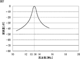
図2は、基本電力伝送システム11の伝送効率の変化の一例を示す図である。
FIG. 2 is a diagram illustrating an example of a change in transmission efficiency of the basic
図2において、縦軸は、伝送効率としての最大伝送効率に対する減衰量[dB]を示し、横軸は、発振周波数f31[MHz]を示している。 In FIG. 2, the vertical axis represents the attenuation [dB] with respect to the maximum transmission efficiency as the transmission efficiency, and the horizontal axis represents the oscillation frequency f31 [MHz].
なお、図2の例では、共振周波数f33,f51は、ISM(Industry Science Medical)バンドである13.56MHzに固定されている。また、試作実験では共振回路33,51のQ値は、いずれも、400程度になった。即ち、Q値は、いずれも、非常に高い値に設定されている。
In the example of FIG. 2, the resonance frequencies f33 and f51 are fixed to 13.56 MHz which is an ISM (Industry Science Medical) band. In the prototype experiment, the Q values of the
図2に示されるように、発振周波数f31が、共振周波数f33,f51(=13.56MHz)から0.5MHz程度とわずかにずれるだけでも、伝送効率が20dB程度と大幅に低下しまうことがわかる。このことは、逆の観点からすると、発振周波数f31が固定されている場合に、金属や人間などが近接して共振周波数f33,f51がわずかでも変化してしまうと、伝送効率が大幅に低下してしまうことを意味している。伝送効率の大幅な低下は、電力の伝送がほとんどできなくなることを意味する。 As can be seen from FIG. 2, even if the oscillation frequency f31 is slightly shifted from the resonance frequencies f33 and f51 (= 13.56 MHz) to about 0.5 MHz, the transmission efficiency is significantly reduced to about 20 dB. From the opposite viewpoint, when the oscillation frequency f31 is fixed, if the resonance frequency f33, f51 changes even slightly due to the proximity of metal or humans, the transmission efficiency is greatly reduced. It means to end up. A significant decrease in transmission efficiency means that almost no power can be transmitted.
<2.第1実施形態> <2. First Embodiment>
そこで、本発明人は、基本電力伝送手法を基礎として、共振周波数を変化させる手法を発明した。なお、以下、かかる手法を共振周波数可変手法と称する。本発明が適用された電力伝送システムのうち、このような共振周波数可変手法が適用された実施形態が、第1実施形態である。 Accordingly, the present inventors have invented a method for changing the resonance frequency based on the basic power transmission method. Hereinafter, this method is referred to as a resonance frequency variable method. Of the power transmission system to which the present invention is applied, an embodiment to which such a resonance frequency variable technique is applied is the first embodiment.
即ち、第1実施形態では、共振周波数可変手法が適用されて、電力伝送システムの使用中でも共振周波数が発振周波数に一致するように制御される。その結果、伝送効率の低下を防止すること、即ち、非接触で電力を安定に伝送することができるようになる。 That is, in the first embodiment, the resonance frequency variable method is applied, and the resonance frequency is controlled to coincide with the oscillation frequency even when the power transmission system is used. As a result, it is possible to prevent a decrease in transmission efficiency, that is, to stably transmit power without contact.
以下、第1実施形態の詳細についてさらに説明する。 Hereinafter, details of the first embodiment will be further described.
[電力伝送システムの第1実施形態の構成例] [Configuration Example of First Embodiment of Power Transmission System]
図3は、本発明が適用された電力伝送システムの第1実施形態の構成例を示している。 FIG. 3 shows a configuration example of the first embodiment of the power transmission system to which the present invention is applied.
図3において、図1の場合と対応する部分には同一の符号を付してあり、その説明は適宜省略する。 3, parts corresponding to those in FIG. 1 are denoted by the same reference numerals, and description thereof will be omitted as appropriate.
図3の例の電力伝送システム81は、送電装置91と受電装置92とを含むように構成される。
The
送電装置91には、図1の場合と同様に、発振回路31および送電コイル32が設けられている。送電装置91にはまた、図1の送電側共振回路33に代えて、送電側共振回路101が設けられている。
As in the case of FIG. 1, the
送電側共振回路101は、図1の送電側共振回路33(数ループ程度のコイル)に対して並列に、バリキャップ112とコンデンサ113とからなる直列回路が接続されている。
The power transmission
ここで、バリキャップ112の容量値をCvsと記述し、コンデンサ113の容量値をCcsと記述すると、送電側共振回路101の共振周波数f101は、次の式(4)のように示される。
Here, when the capacitance value of the
式(4)において、コンデンサ113の容量値Ccsは所定の固定値であるのに対して、バリキャップ112の容量値Cvsは可変値である。バリキャップ112は、バラクタや可変容量ダイオードなどとも称される素子であって、印加電圧が増加するに連れて容量値Cvsが減少するという特性を有しているからである。
In Expression (4), the capacitance value Ccs of the
即ち、バリキャップ112の印加電圧を変化させることで、その容量値Cvsが変化するので、結果として、送電側共振回路101の共振周波数f101を変化させることができる。従って、送電側共振回路101の共振周波数f101を発振周波数f33に一致させるように変化させることで、伝送効率の低下を防止すること、即ち、非接触で電力を安定に伝送することができるようになる。
That is, since the capacitance value Cvs is changed by changing the voltage applied to the
換言すると、送電側共振回路101の共振周波数f101を発振周波数f33に一致させるように変化させるためには、バリキャップ112の容量値Cvsの適切な制御、即ち、バリキャップ112の印加電圧の適切な制御を行うと好適である。そこで、かかる制御(以下、送電側共振周波数可変制御と称する)を実現すべく、送電装置91にはさらに、アンテナ102、受信回路103、およびD/A(Digital to Analog)変換回路104が設けられている。
In other words, in order to change the resonance frequency f101 of the power transmission
受信回路103は、受電装置92から送信されてきた制御データを、アンテナ102を介して受信する。詳細については後述するが、この制御データには、バリキャップ112の印加電圧の変更命令等が含まれている。
The receiving
そこで、受信回路103は、制御データに基づいて、バリキャップ112の印加電圧の指令(デジタルデータ)を生成し、D/A変換回路104に供給する。D/A変換回路104は、受信回路103からの指令に従って、バリキャップ112の印加電圧を変化させる。即ち、D/A変換回路104は、受信回路103からのデジタルデータ(指令)に対応するアナログ電圧を、バリキャップ112に印加する。
Therefore, the receiving
これにより、バリキャップ112の容量値Cvsは変更され、その結果、送電側共振回路101の共振周波数f101は変化することになる。
Thereby, the capacitance value Cvs of the
このように、送電側共振周波数可変制御は、受電装置92から送信されてきた制御データに基づいて実行される。なお、送電側共振周波数可変制御の詳細については、図5を用いて後述する。
As described above, the power transmission side resonance frequency variable control is executed based on the control data transmitted from the
このような送電装置91に対して、受電装置92には、図1の場合と同様に、受電コイル52、ブリッジ整流回路53、および平滑コンデンサ54が設けられている。受電装置92にはまた、その前段に、図1の受電側共振回路51に代えて、受電側共振回路121が設けられている。
For such a
受電側共振回路121は、図1の受電側共振回路51(数ループ程度のコイル)に対して並列に、バリキャップ132とコンデンサ133とからなる直列回路が接続されている。
The power receiving
ここで、バリキャップ132の容量値をCvrと記述し、コンデンサ133の容量値をCcrと記述すると、受電側共振回路121の共振周波数f121は、次の式(5)のように示される。
Here, when the capacitance value of the
式(5)において、上述の式(4)と同様の理由により、コンデンサ133の容量値Ccrは所定の固定値であるのに対して、バリキャップ132の容量値Cvrは可変値である。バリキャップ132は、バラクタや可変容量ダイオードなどとも称される素子であって、印加電圧が増加するに連れて容量値Cvrが減少するという特性を有しているからである。
In the equation (5), for the same reason as the above equation (4), the capacitance value Ccr of the
即ち、バリキャップ132の印加電圧を変化させることで、その容量値Cvrは変化するので、結果として、受電側共振回路121の共振周波数f121を変化させることができる。これにより、受電側共振回路121の共振周波数f121を発振周波数f33に一致させるように変化させることで、伝送効率の低下を防止すること、即ち、非接触で電力を安定に伝送することができるようになる。
That is, by changing the voltage applied to the
換言すると、受電側共振回路121の共振周波数f121を発振周波数f33に一致させるように変化させるためには、バリキャップ132の容量値Cvrの適切な制御、即ち、バリキャップ132の印加電圧の適切な制御を行うと好適である。そこで、かかる制御(以下、受電側共振周波数可変制御と称する)を実現すべく、受電装置92にはさらに、A/D変換回路122、マイクロコンピュータ123、およびD/A変換回路124が設けられている。
In other words, in order to change the resonance frequency f121 of the power reception
A/D変換回路122は、平滑コンデンサ54の両端のアナログ電圧を、デジタルデータである出力電圧値Vに変換して、マイクロコンピュータ123に供給する。
The A /
マイクロコンピュータ123は、受電装置92の動作全体を制御する。
The
例えば、マイクロコンピュータ123は、A/D変換回路12の出力電圧値Vに基づいて、受電側のバリキャップ132の印加電圧の指令(デジタルデータ)を生成し、D/A変換回路124に供給する。
For example, the
D/A変換回路124は、マイクロコンピュータ123からの指令に従って、バリキャップ132の印加電圧を変化させる。即ち、D/A変換回路124は、マイクロコンピュータ123からのデジタルデータ(指令)に対応するアナログ電圧を、バリキャップ132に印加する。
The D /
これにより、バリキャップ132の容量値Cvrは変更され、その結果、受電側共振回路121の共振周波数f121は変化することになる。
As a result, the capacitance value Cvr of the
このように、受電側共振周波数可変制御は、A/D変換回路12の出力電圧値Vに基づいて実行される。なお、受電側共振周波数可変制御の詳細については、図4を用いて後述する。
Thus, the power receiving side resonance frequency variable control is executed based on the output voltage value V of the A /
また例えば、マイクロコンピュータ123は、A/D変換回路12の出力電圧値Vに基づいて、送信側のバリキャップ112の印加電圧の変更命令等を含む制御データを生成する。
Further, for example, the
この制御データは、上述したように、送電側共振周波数可変制御に用いられる。よって、この制御データは、送電装置91に転送される必要がある。このため、受電装置92にはさらに、送信回路125およびアンテナ126が設けられている。
As described above, this control data is used for power transmission side resonance frequency variable control. Therefore, this control data needs to be transferred to the
即ち、マイクロコンピュータ123により生成された制御データは、送信回路125に供給される。そこで、送信回路125は、マイクロコンピュータ123からの制御データを、アンテナ126を介して送電装置91に送信する。すると、上述したように、送電装置91は、この制御データを用いて、送電側のバリキャップ112の印加電圧を変化させる。これにより、その容量値Cvsが変化して、送電側共振回路101の共振周波数f101が変化することになる。このようにして、送電側共振周波数可変制御を実行する。なお、送電側共振周波数可変制御のさらなる詳細については、図4を用いて後述する。
That is, the control data generated by the
[電力伝送システムの第1実施形態の動作例] [Operation Example of First Embodiment of Power Transmission System]
次に、図3の例の電力伝送システム81の動作例について説明する。
Next, an operation example of the
ただし、電力伝送システム81の動作のうち、送電装置91から受電装置92への電力伝送の動作自体は、図1の基本電力伝送システム11の動作と基本的に同様であるので、ここではその説明は省略する。
However, among the operations of the
そこで、以下、電力伝送システム81の動作のうち、受電側共振周波数可変制御と送電側共振周波数可変制御とを実現する処理(以下、共振周波数制御処理と称する)について説明する。
Therefore, a process (hereinafter referred to as a resonance frequency control process) for realizing the power receiving side resonance frequency variable control and the power transmission side resonance frequency variable control in the operation of the
送電装置91から受電装置92に供給された電力を、以下、受電電力と称し、受電電力をPと記述すると、受電電力Pは、次の式(6)により示される。
The power supplied from the
なお、式(6)において、Rは、受電装置92の負荷の抵抗値を示している。
In Equation (6), R represents the resistance value of the load of the
ここで、送電側共振周波数可変制御や受電側共振周波数可変制御とは、共振周波数f101,f121を変化させて発振周波数f33に一致させる制御である。上述した図2を用いて説明したように、共振周波数f101,f121が発振周波数f33に一致しているときが、伝送効率が最も高いので、受電電力Pが最大となる。即ち、送電側共振周波数可変制御や受電側共振周波数可変制御として、受電電力Pが最大となるように、共振周波数f101,f121を変化させる制御を採用すればよい。さらに言えば、式(6)に示されるように、固定負荷であれば負荷の抵抗値Rは一定であり、受電電力Pは、出力電圧値Vの自乗に比例する。従って、受電側共振周波数可変制御として、出力電圧値Vが最大となるように、共振周波数f101,f121を変化させる制御を採用すればよい。このような受電側共振周波数可変制御と送電側共振周波数可変制御とを実現する共振周波数制御処理の一例が図4に示されている。 Here, the power transmission side resonance frequency variable control and the power reception side resonance frequency variable control are controls in which the resonance frequencies f101 and f121 are changed to coincide with the oscillation frequency f33. As described with reference to FIG. 2 described above, when the resonance frequencies f101 and f121 match the oscillation frequency f33, the transmission efficiency is the highest, and thus the received power P is maximum. That is, as power transmission side resonance frequency variable control and power reception side resonance frequency variable control, control for changing the resonance frequencies f101 and f121 so as to maximize the received power P may be employed. Furthermore, as shown in the equation (6), if the load is fixed, the resistance value R of the load is constant, and the received power P is proportional to the square of the output voltage value V. Therefore, as power reception-side resonance frequency variable control, control for changing the resonance frequencies f101 and f121 so as to maximize the output voltage value V may be employed. An example of a resonance frequency control process for realizing such a power receiving side resonance frequency variable control and a power transmission side resonance frequency variable control is shown in FIG.
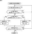
図4は、共振周波数制御処理の一例を説明するフローチャートである。 FIG. 4 is a flowchart for explaining an example of the resonance frequency control process.
ステップS11において、マイクロコンピュータ123は、受電側のバリキャップ132の印加電圧の指令を1ステップずつ増加させ、ステップ毎の各出力電圧値Vを計測する。
In step S11, the
ステップS12において、マイクロコンピュータ123は、出力電圧値Vが最大となったときの指令を、受電側のバリキャップ132の最適指令として設定する。
In step S <b> 12, the
その後、マイクロコンピュータ123は、その最適指令(デジタルデータ)を、D/A変換回路124に出力し続ける。これにより、受電側共振回路121の共振周波数f121は、出力電圧値Vが最大となる周波数、即ち、発振周波数f33にほぼ一致した周波数になる。
Thereafter, the
より具体的には例えば、バリキャップ132の印加電圧が上昇すると、上述したように、バリキャップ132の容量値Cvrは減少し、上述した式(5)に示されるように、受電側共振回路121の共振周波数f121は高くなる。逆に、バリキャップ132の印加電圧が下降すると、上述したように、バリキャップ132の容量値Cvrは増加し、上述した式(5)に示されるように、受電側共振回路121の共振周波数f121は低くなる。
More specifically, for example, when the applied voltage of the
従って、受電側共振回路121の共振周波数f121を発振周波数f33にほぼ一致させるためには、共振周波数f121を高い方向にも低い方向にも調整できるようにしておく必要がある。即ち、金属や人間などが近接した場合でも、受電電力Pが最大となるバリキャップ132の容量値Cvrが、その可変範囲内に入るように、バリキャップ132の容量値Cvrを増加方向にも減少方向にも調整できるようにしておく必要がある。さらにいえば、バリキャップ132は特性のバラつきがあるので、そのようなバラつきも考慮した上で調整できるようにしておく必要がある。
Therefore, in order to make the resonance frequency f121 of the power reception
このような調整を可能にすべく、バリキャップ132の容量値Cvrがその可変範囲のうち中間容量値となったときに、金属や人間などが近接していない理想的な状態における共振周波数f121が、目的の周波数(発振周波数f33)となると好適である。そこで、例えば本実施形態では、そうなるように、受電側共振回路121のコイルのインダクタンスLrや、コンデンサ133の容量Ccrが調整されている。
In order to enable such adjustment, when the capacitance value Cvr of the
従って、例えば本実施形態では、ステップS11の処理で、受電側のバリキャップ132の印加電圧の指令が1ステップずつ増加された場合、最高のステップの指令に至るまでの特定のステップで、出力電圧値Vが最大になるはずである。例えば、金属や人間などが近接していない理想的な状態では、受電側のバリキャップ132の印加電圧の指令の可変範囲のうちほぼ中間のステップで、出力電圧値Vが最大になるはずである。また例えば、金属や人間などが近接している状態では、中間のステップの前後に若干ずれたステップで、出力電圧値Vが最大になるはずである。
Therefore, for example, in this embodiment, when the command of the voltage applied to the power receiving
例えば、図5は、受電側のバリキャップ132の印加電圧と、出力電圧値Vとの関係を示している。
For example, FIG. 5 shows the relationship between the voltage applied to the
図5において、縦軸は出力電圧値Vを示している。また、横軸は、受電側のバリキャップ132の印加電圧を示している。
In FIG. 5, the vertical axis represents the output voltage value V. The horizontal axis represents the voltage applied to the
図5の例では、出力電圧値Vは山型の形状で変化し、受電側のバリキャップ132の印加電圧が約10Vで、山の頂上になっていること、即ち出力電圧値Vが最大になっていることがわかる。
In the example of FIG. 5, the output voltage value V changes in a mountain shape, the applied voltage of the
そこで、ステップS12の処理では、出力電圧値Vが最大となったときの指令(デジタルデータ)、図5の例では約10V前後のステップの指令が、受電側のバリキャップ132の最適指令として設定されるのである。
Therefore, in the process of step S12, a command (digital data) when the output voltage value V is maximum, and a command of a step of about 10 V in the example of FIG. 5 is set as the optimum command for the
このように、ステップS11,S12の処理で、受電側共振周波数可変制御が実現されることになる。 Thus, the power receiving side resonance frequency variable control is realized by the processing of steps S11 and S12.
次に、ステップS13以降の処理で、送電側共振周波数可変制御が実現されることになる。 Next, power transmission side resonance frequency variable control is realized by the processing after step S13.
即ち、ステップS13において、マイクロコンピュータ123は、送電側のバリキャップ112の印加電圧の指令を1ステップずつ増加させ、ステップ毎の各出力電圧値Vを計測する。
That is, in step S13, the
具体的には例えば、マイクロコンピュータ123は、送電側のバリキャップ112の印加電圧の指令を1ステップ増加させる変更命令等を含む制御データを生成し、送信回路125およびアンテナ126を介して送電装置91に送信する。すると、送電装置91は、上述したように、その制御データに従って、送電側のバリキャップ112の印加電圧を1ステップ増加させる。これにより、その容量値Cvsが変化して、送電側共振回路101の共振周波数f101が変化するので、その結果として、受電装置92の出力電圧値Vが変化する。そこで、マイクロコンピュータ123は、変化した出力電圧値Vを計測する。ステップS13の処理として、このような一連の処理が、各ステップ毎に実行される。
Specifically, for example, the
なお、送電側のバリキャップ132と同様の理由により、バリキャップ112の容量値Cvsがその可変範囲のうち中間容量値となったときに、金属や人間などが近接していない理想的な状態における共振周波数f101が、目的の周波数(発振周波数f33)となると好適である。そこで、例えば本実施形態では、そうなるように、送電側共振回路101のコイルのインダクタンスLsや、コンデンサ133の容量Ccsが調整されている。
Note that, for the same reason as the
ステップS14において、マイクロコンピュータ123は、出力電圧値Vが最大となったときの指令を、送電側のバリキャップ112の最適指令として設定する。
In step S <b> 14, the
具体的には例えば、マイクロコンピュータ123は、送電側のバリキャップ112の印加電圧の最適指令の設定命令等を含む制御データを生成し、送信回路125やおよびアンテナ126を介して送電装置91に送信する。
Specifically, for example, the
すると、送電装置91は、その最適指令に従った印加電圧を、送電側のバリキャップ112に印加し続ける。これにより、送電側共振回路101の共振周波数f101は、出力電圧値Vが最大となる周波数、即ち、発振周波数f33にほぼ一致した周波数になる。
Then, the
このように、第1実施形態の電力伝送システム81では、共振周波数制御処理が実行される。これにより、受電電力Pが最大となるように共振周波数が自動的に制御されることになる。その結果、送電装置91から受電装置92に対して、安定して電力を供給することができるようになる。
Thus, in the
このことは、共振周波数f101,f121がばらついたとしても、何ら変わりはない。即ち、第1実施形態の電力伝送システム81では、共振周波数制御処理が実行されるので、共振周波数f101,f121のばらつきが許容されることになる。その結果、従来の磁界共鳴型電力伝送手法が適用された非接触電力システムと比較すると、第1実施形態の電力伝送システム81を量産することが容易に可能になる。即ち、従来の磁界共鳴型電力伝送手法が適用された非接触電力システムでは、共振周波数制御処理は実行できないので、共振周波数のばらつきは許容できないことになる。しかしながら、共振周波数の製造上のばらつきを抑えることが困難であり、その結果、従来の磁界共鳴型電力伝送手法が適用された非接触電力システムを量産することは困難であった。この困難性が、第1実施形態の電力伝送システム81では共振周波数f101,f121のばらつきが許容されるので、解消されるのである。
This does not change even if the resonance frequencies f101 and f121 vary. That is, in the
なお、図4の共振周波数制御処理の開始タイミングは、特に限定されない。例えば、開始タイミングとしては、受電装置92が通電されるタイミングを採用することができる。また例えば、出力電圧値Vが低下したタイミング、所定時間が経過したタイミング、ユーザにより指示されたタイミング等を開始タイミングとして採用することができる。
Note that the start timing of the resonance frequency control process of FIG. 4 is not particularly limited. For example, a timing at which the
また、共振周波数制御処理では、受電側共振周波数可変制御と送電側共振周波数可変制御との2つの制御が実現された。しかしながら、これらの2つの制御のうち、いずれか一方のみが行われるようにすることができる。例えば、送電側共振回路101と受電側共振回路121のうち、一方が人や金属が近接しない離れた場所に配置されていてそれらの影響を受けない場合、他方の共振周波数のみを制御するようにしてもよい。
Also, in the resonance frequency control process, two controls of the power receiving side resonance frequency variable control and the power transmission side resonance frequency variable control are realized. However, only one of these two controls can be performed. For example, when one of the power transmission
また、受電側共振周波数可変制御と送電側共振周波数可変制御を実現するという視点では、それらの制御手法は、受電電力Pが最大となるように共振周波数を制御できる手法であれば足り、上述の手法に特に限定されない。 Further, from the viewpoint of realizing the power receiving side resonance frequency variable control and the power transmission side resonance frequency variable control, those control methods may be any methods that can control the resonance frequency so that the received power P is maximized. The method is not particularly limited.
例えば、共振周波数を変化させる手法(以下、共振周波数可変手法と称する)として、上述の例では、バリキャップ112,113の印加電圧を変化させる手法が採用された。しかしながら、共振周波数可変手法は、上述の例に特に限定されず、例えばバリキャップ以外の素子、モータ駆動のバリコン(可変抵抗器)を用いて、共振回路のインダクタンスLやキャパシタンスCを変化させる手法を採用することができる。また例えば、共振回路を構成するコイルのコアの出し入れやコイルの間隔を変えたり、コイルのタップ出しを電気的切り換えることで、インダクタンスLを変化させる手法を採用することができる。
For example, as a method for changing the resonance frequency (hereinafter referred to as a resonance frequency variable method), in the above-described example, a method of changing the voltage applied to the
<3.第2実施形態> <3. Second Embodiment>
さらにいえば、伝送効率を最大にするという視点、即ち、受電電力Pを最大にするという視点からすれば、共振周波数と発振周波数とを一致させるような制御をすれば足りる。 Furthermore, from the viewpoint of maximizing the transmission efficiency, that is, from the viewpoint of maximizing the received power P, it is sufficient to perform control so that the resonance frequency and the oscillation frequency coincide with each other.
即ち、第1実施形態では、発振周波数を固定して、共振周波数を変化させることで、共振周波数と発振周波数f31とを一致させる制御として、受電側共振周波数可変制御と送電側共振周波数可変制御が採用された。 In other words, in the first embodiment, as the control for matching the resonance frequency and the oscillation frequency f31 by changing the resonance frequency while fixing the oscillation frequency, the power receiving side resonance frequency variable control and the power transmission side resonance frequency variable control are performed. Adopted.
しかしながら、受電電力Pを最大にするという視点からすれば、共振周波数の方を固定して、発振周波数を変化させることで、共振周波数と発振周波数とを一致させる制御も実現可能である。以下、かかる制御を、発振周波数可変制御と称する。 However, from the viewpoint of maximizing the received power P, it is also possible to realize a control for matching the resonance frequency and the oscillation frequency by fixing the resonance frequency and changing the oscillation frequency. Hereinafter, such control is referred to as oscillation frequency variable control.
換言すると、本発明人は、基本電力伝送手法を基礎とした手法として、共振周波数変化手法に加えてさらに、発振周波数可変制御を実現させる手法(以下、発振周波数可変手法と称する)を発明した。本発明が適用された電力伝送システムのうち、このような発振周波数可変手法が適用された実施形態が、第2実施形態である。 In other words, the present inventors have invented a technique (hereinafter referred to as an oscillation frequency variable technique) that realizes an oscillation frequency variable control in addition to the resonance frequency change technique as a technique based on the basic power transmission technique. Of the power transmission system to which the present invention is applied, an embodiment to which such an oscillation frequency variable technique is applied is a second embodiment.
即ち、第2実施形態では、発振周波数可変手法が適用されて、電力伝送システムの使用中でも発振周波数f31が共振周波数に一致するように制御される。その結果、伝送効率の低下を防止すること、即ち、非接触で電力を安定に伝送することができるようになる。 That is, in the second embodiment, the oscillation frequency variable method is applied, and the oscillation frequency f31 is controlled to coincide with the resonance frequency even during use of the power transmission system. As a result, it is possible to prevent a decrease in transmission efficiency, that is, to stably transmit power without contact.
以下、第2実施形態の詳細についてさらに説明する。 The details of the second embodiment will be further described below.
[電力伝送システムの第2実施形態の構成例] [Configuration Example of Second Embodiment of Power Transmission System]
図6は、本発明が適用された電力伝送システムの第2実施形態の構成例を示している。 FIG. 6 shows a configuration example of the second embodiment of the power transmission system to which the present invention is applied.
図6において、図1または図3の場合と対応する部分には同一の符号を付してあり、その説明は適宜省略する。 In FIG. 6, the same reference numerals are given to the portions corresponding to those in FIG. 1 or FIG.
図6の例の電力伝送システム161は、送電装置171と受電装置172とを含むように構成される。
The
図1との比較の視点からすると、送電装置171には、図1の場合と同様に、送電コイル32および送電側共振回路33が設けられている。送電装置171にはまた、図1の発振回路31に代えて、発振回路181が設けられている。送電装置171にはさらに、アンテナ102と受信回路103が設けられている。
From the viewpoint of comparison with FIG. 1, the
図3との比較の視点からすると、送電装置171には、図3の発振回路31に代えて発振回路181が設けられ、図3の送電側共振回路101に代えて、図1の場合と同様の送電側共振回路33が設けられている。送電装置171にはまた、図3の場合と同様に、送電コイル32、アンテナ102、および受信回路103が設けられている。一方、送電装置171の構成要素としては、図3の送電装置91の構成要素の1つであるD/A変換回路104は省略されている。
From the viewpoint of comparison with FIG. 3, the
発振回路181は、その発振周波数f181を可変すべく、基準周波数発生回路191、位相同期回路192、および増幅回路193を含むように構成されている。
The
基準周波数発生回路191は、基準周波数の電気信号を発生し、位相同期回路192に供給する。位相同期回路192は、例えば、PLL(Phase-locked loop)回路により構成される。位相同期回路192には、基準周波数の倍率N(Nは1以上の数値)が設定されている。即ち、位相同期回路192は、基準周波数の電気信号に対して所定の処理を施すことで、基準周波数のN倍の周波数の電気信号を生成し、増幅回路193に供給する。増幅回路193は、位相同期回路192の出力信号を増幅して、増幅後の電気信号を出力する。この増幅回路193の出力信号が、発振回路181の出力信号である。
The reference
このようにして、発振回路181の発振周波数f181は、基準周波数のN倍の周波数となる。即ち、位相同期回路192のN値の設定を変化させることで、発振周波数f181を変化させることができるようになる。
In this way, the oscillation frequency f181 of the
位相同期回路192のN値の設定は、受信回路103によりなされる。即ち、受信回路103は、受電装置172から送信されてきた制御データを、アンテナ102を介して受信する。詳細については後述するが、この制御データには、N値の変更命令等が含まれている。そこで、受信回路103は、制御データに基づいて、位相同期回路192のN値の設定を変更する。
The N value of the
このように、発振周波数可変制御は、受電装置172から送信されてきた制御データに基づいて実行される。なお、発振周波数可変制御のさらなる詳細については、図7を用いて後述する。
As described above, the oscillation frequency variable control is executed based on the control data transmitted from the
このような構成の送電装置171に対して、受電装置172の構成は、図1との比較の視点からすると次のようになる。即ち、受電装置172には、図1の場合と同様に、受電側共振回路51、受電コイル52、ブリッジ整流回路53、および平滑コンデンサ54が設けられている。受電装置172にはさらに、A/D変換回路122、マイクロコンピュータ123、D/A変換回路124、送信回路125、および、アンテナ126が設けられている。
With respect to the
図3との比較の視点からすると、受電装置172には、図3の受電側共振回路121に代えて、図1の場合と同様の受電側共振回路51が設けられている。また、受電装置172の構成要素としては、図3の受電装置92の構成要素の1つであるD/A変換回路124は省略されている。その他の受電装置172の構成は、図3の場合と同様である。
From the viewpoint of comparison with FIG. 3, the
[電力伝送システムの第2実施形態の動作例] [Operation Example of Second Embodiment of Power Transmission System]
次に、図6の例の電力伝送システム161の動作例について説明する。
Next, an operation example of the
ただし、電力伝送システム161の動作のうち、送電装置171から受電装置172への電力伝送の動作自体は、図1の基本電力伝送システム11の動作と基本的に同様であるので、ここではその説明は省略する。
However, among the operations of the
そこで、以下、電力伝送システム161の動作のうち、発振周波数可変制御を実現する処理(以下、発振周波数制御処理と称する)について説明する。
Therefore, a process for realizing the oscillation frequency variable control (hereinafter referred to as an oscillation frequency control process) in the operation of the
図7は、発振周波数制御処理の一例を説明するフローチャートである。 FIG. 7 is a flowchart for explaining an example of the oscillation frequency control process.
ステップS31において、マイクロコンピュータ123は、送電側のN値を1ステップずつ増加させ、ステップ毎の各出力電圧値Vを計測する。
In step S31, the
具体的には例えば、マイクロコンピュータ123は、送電側のN値を1ステップ増加させる変更命令等を含む制御データを生成し、送信回路125やおよびアンテナ126を介して送電装置171に送信する。すると、送電装置171は、上述したように、その制御データに従って、位相同期回路192のN値を1ステップ増加させる。これにより、発振回路181の発振周波数f181が変化するので、その結果として、受電装置172の出力電圧値Vが変化する。そこで、マイクロコンピュータ123は、変化した出力電圧値Vを計測する。ステップS31の処理として、このような一連の処理が、各ステップ毎に実行される。
Specifically, for example, the
ステップS32において、マイクロコンピュータ123は、出力電圧値Vが最大となったときの指令を、送電側のN値の最適指令として設定する。
In step S <b> 32, the
具体的には例えば、マイクロコンピュータ123は、送電側のN値の最適指令の設定命令等を含む制御データを生成し、送信回路125やおよびアンテナ126を介して送電装置171に送信する。
Specifically, for example, the
すると、送電装置171は、位相同期回路192のN値として、その最適指令に従ったステップの値を設定する。これにより、発振回路181の発振周波数f181は、出力電圧値Vが最大となる周波数、即ち、送信側共振回路33の共振周波数f33や受電側共振回路51の共振周波数f51にほぼ一致した周波数になる。
Then, the
このように、第2実施形態の電力伝送システム161では、発振周波数制御処理が実行される。これにより、受電電力Pが最大となるように発振周波数が自動的に制御されることになる。その結果、送電装置171から受電装置172に対して、安定して電力を供給することができるようになる。また、第1実施形態の場合と同様の理由により、第2実施形態の電力伝送システム161もまた量産することが容易に可能になる。
Thus, in the
<4.第3実施形態> <4. Third Embodiment>
ところで、上述した第1実施形態と第2実施形態においては、送電側と受電側の間の距離(以下、伝送距離と称する)は固定されていた。しかしながら、例えば受電装置が携帯端末などで構成されて持ち運び自在になる場合などには、伝送距離が変わってしまう場合もあり得る。 By the way, in 1st Embodiment and 2nd Embodiment mentioned above, the distance (henceforth a transmission distance) between the power transmission side and the power receiving side was fixed. However, for example, when the power receiving device is configured by a portable terminal or the like and is portable, the transmission distance may change.
この場合、伝送距離に反比例して受電電力Pが変化する。よって、伝送距離が可変する場合に何ら対策を施さないと、例えば、伝送距離が短い場合、受電電力Pが、受電側で必要とされる電力(以下、必要電力と称する)以上となってしまい、不要輻射が増大したり無駄な電力が消費されるおそれもある。一方、伝送距離が長い場合、受電電力Pが必要電力未満となってしまい、受電側の動作に支障をきたすおそれもある。 In this case, the received power P changes in inverse proportion to the transmission distance. Therefore, if no measures are taken when the transmission distance is variable, for example, when the transmission distance is short, the received power P is greater than or equal to the power required on the power receiving side (hereinafter referred to as necessary power). Unnecessary radiation may increase or wasteful power may be consumed. On the other hand, when the transmission distance is long, the received power P becomes less than the required power, which may hinder the operation on the power receiving side.
即ち、受電電力Pを必要電力で維持することが好適であるところ、伝送距離が可変する場合に何ら対策を施さないと、受電電力Pは必要電力で維持することは困難になる。 That is, it is preferable to maintain the received power P with the required power. However, if no measures are taken when the transmission distance varies, it is difficult to maintain the received power P with the required power.
そこで、本発明人は、受電電力Pを必要電力で維持すべく、基本電力伝送手法を基礎として、送電装置91の出力電力(以下、送電電力と称する)を制御する手法を発明した。なお、以下、かかる制御を送電電力可変制御と称し、かかる手法を送電電力可変手法と称する。
Therefore, the present inventors have invented a method for controlling the output power (hereinafter referred to as transmitted power) of the
[送電電力可変手法] [Transmission power variable method]
図8は、送電電力可変手法を説明する図である。 FIG. 8 is a diagram illustrating a transmission power variable method.
図8において、縦軸は、受電電力Pを示し、横軸は、伝送距離を示している。 In FIG. 8, the vertical axis represents the received power P, and the horizontal axis represents the transmission distance.
図8の例では、説明の簡略上、送電電力が、「低」、「中」、「高」の3段階に可変できるとする。この場合、送電電圧が「低」の場合の伝送距離に対する受電電力Pの変化が、曲線PP1により示されている。送電電力が「中」の場合の伝送距離に対する受電電力Pの変化が、曲線PP2により示されている。送電電力が「高」の場合の伝送距離に対する受電電力Pの変化が、曲線PP3により示されている。 In the example of FIG. 8, for the sake of simplicity, it is assumed that the transmission power can be varied in three stages of “low”, “medium”, and “high”. In this case, a change in the received power P with respect to the transmission distance when the transmission voltage is “low” is indicated by a curve PP1. A change in the received power P with respect to the transmission distance when the transmitted power is “medium” is indicated by a curve PP2. A change in the received power P with respect to the transmission distance when the transmitted power is “high” is indicated by a curve PP3.
いま、例えば、伝送距離が距離D2であり、送電電力が「中」であるとする。この場合、受電電力Pは必要電力となっている。即ち、伝送距離が距離D2の場合には、送電電力が「中」となるように制御されると好適である。 Now, for example, assume that the transmission distance is the distance D2 and the transmitted power is “medium”. In this case, the received power P is required power. That is, when the transmission distance is the distance D2, it is preferable that the transmission power is controlled to be “medium”.
しかしながら、例えば、その後、伝送距離が比較的短い距離D1に変化した場合、送電電力が「中」のまま維持されていると、受電電力Pは必要電力を超えてしまうことになる。そこで、このような場合、送電電力可変制御として、送電電力を「中」から「低」に変化させる制御が実行され、その結果、受電電力Pを必要電力のまま維持させることができる。 However, for example, when the transmission distance subsequently changes to a relatively short distance D1, if the transmission power is maintained at “medium”, the received power P exceeds the required power. Therefore, in such a case, as the transmission power variable control, control for changing the transmission power from “medium” to “low” is executed, and as a result, the received power P can be maintained as it is.
また例えば、その後、伝送距離が比較的長い距離D3に変化した場合、送電電力が「小」のまま維持されていると、受電電力Pは必要電力未満になってしまうことになる。そこで、このような場合、送電電力可変制御として、送電電力を「低」から「高」に変化させる制御が実行され、その結果、受電電力Pを必要電力のまま維持させることができる。 Further, for example, when the transmission distance subsequently changes to a relatively long distance D3, the received power P will be less than the required power if the transmitted power is kept “low”. Therefore, in such a case, control for changing the transmission power from “low” to “high” is executed as the transmission power variable control, and as a result, the received power P can be maintained as it is.
本発明が適用された電力伝送システムのうち、このような送電電力可変手法が適用された実施形態が、第3実施形態である。 Of the power transmission system to which the present invention is applied, an embodiment to which such a variable transmission power technique is applied is a third embodiment.
即ち、第3実施形態では、送電電力可変手法が適用されて、伝送距離によらず、受電電力Pが必要電力を維持するように制御される。その結果、非接触で電力を安定に伝送することができるようになる。 That is, in the third embodiment, the transmission power variable method is applied, and the received power P is controlled to maintain the required power regardless of the transmission distance. As a result, power can be stably transmitted without contact.
以下、第3実施形態の詳細についてさらに説明する。 Hereinafter, details of the third embodiment will be further described.
[電力伝送システムの第1実施形態の構成例] [Configuration Example of First Embodiment of Power Transmission System]
図9は、本発明が適用された電力伝送システムの第3実施形態の構成例を示している。 FIG. 9 shows a configuration example of a third embodiment of the power transmission system to which the present invention is applied.
図9において、図1の場合と対応する部分には同一の符号を付してあり、その説明は適宜省略する。 9, parts corresponding to those in FIG. 1 are denoted by the same reference numerals, and description thereof will be omitted as appropriate.
図9の例の電力伝送システム221は、送電装置231と受電装置232とを含むように構成される。
The
送電装置231には、図1の場合と同様に、発振回路31、送電コイル32、および、送電側共振回路33が設けられている。さらに、送電装置91には、発振回路31と送電コイル32の間に増幅回路241が設けられている。さらにまた、送電装置91には、送電電力制御回路242、マイクロコンピュータ243、受信回路244、およびアンテナ245が設けられている。
As in the case of FIG. 1, the
受電装置232には、図1の場合と同様に、受電側共振回路51、受電コイル52、ブリッジ整流回路53、および平滑コンデンサ54が設けられている。さらに、受電装置232には、その後段に、A/D変換回路251が設けられている。さらにまた、受電装置232には、マイクロコンピュータ252、送信回路253、およびアンテナ254が設けられている。
As in the case of FIG. 1, the
受電装置232側のA/D変換回路251は、平滑コンデンサ54の両端のアナログ電圧を、デジタルデータである出力電圧値Vに変換して、マイクロコンピュータ123に供給する。
The A /
受電装置232側のマイクロコンピュータ252は、受電装置232の動作全体を制御する。例えば、マイクロコンピュータ252は、A/D変換回路251の出力電圧値Vに基づいて、送電電力の変更命令等を含む制御データを生成し、送信回路253に供給する。
The
受電装置232側の送信回路125は、マイクロコンピュータ252からの制御データを、アンテナ254を介して送電装置231に送信する。
The
送電装置231側の受信回路244は、受電装置232から送信されてきた制御データを、アンテナ245を介して受信して、マイクロコンピュータ243に供給する。
The
送電装置231側のマイクロコンピュータ243は、送電装置231の動作全体を制御する。例えば、マイクロコンピュータ243は、制御データに基づいて、送電電力の変更命令を生成して、送電電力制御回路242に供給する。
The
送電電力制御回路242は、送電電力の変更命令に従って、増幅回路241のゲイン(増幅率)を設定する。増幅回路241は、発振回路31の出力信号を、設定されたゲイン分だけ増幅する。
The transmission
なお、ゲインとして、設定前の値より低い値が設定された場合には、「設定されたゲイン分だけ増幅する」とは、発振回路31の出力信号のレベルが下降して、その分だけ、送電電力が低くなることになることを意味する。これに対して、ゲインとして、設定前の値より高い値が設定された場合には、「設定されたゲイン分だけ増幅する」とは、発振回路31の出力信号のレベルが上昇して、その分だけ、送電電力が高くなることを意味する。また、ゲインとして、設定前の値と同一値が設定された場合(ゲインの設定変更がなされない場合)には、「設定されたゲイン分だけ増幅する」とは、発振回路31の出力信号のレベルは維持されて、その結果、送電電力も現状のまま維持されることを意味する。
When a value lower than the pre-setting value is set as the gain, “amplify by the set gain” means that the level of the output signal of the
[電力伝送システムの第3実施形態の動作例] [Example of Operation of Third Embodiment of Power Transmission System]
次に、図9の例の電力伝送システム221の動作例について説明する。
Next, an operation example of the
ただし、電力伝送システム221の動作のうち、送電装置231から受電装置232への電力伝送の動作自体は、図1の基本電力伝送システム11の動作と基本的に同様であるので、ここではその説明は省略する。
However, among the operations of the
そこで、以下、電力伝送システム221の動作のうち、送電電力可変制御を実現する処理(以下、送電電力制御処理と称する)について説明する。
Therefore, a process for realizing the transmission power variable control (hereinafter referred to as a transmission power control process) in the operation of the
図10は、送電電力制御処理の一例を説明するフローチャートである。 FIG. 10 is a flowchart illustrating an example of the transmission power control process.
ステップS51において、マイクロコンピュータ252は、出力電圧値Vを計測する。
In step S51, the
ステップS52において、マイクロコンピュータ252は、出力電圧値Vが、必要電力に対応する適切な値(以下、適切値と称する)となっているか否かを判定する。
In step S52, the
出力電圧値Vが適切値となっている場合には、ステップS52においてYESであると判定され、処理はステップS51に戻され、それ以降の処理が繰り返される。即ち、出力電圧値Vが適切値となっている限り、ステップS51,S52のループ処理が繰り返し実行されて、送電電力は現状のまま維持されることになる。 If the output voltage value V is an appropriate value, it is determined as YES in step S52, the process returns to step S51, and the subsequent processes are repeated. That is, as long as the output voltage value V is an appropriate value, the loop processing of steps S51 and S52 is repeatedly executed, and the transmission power is maintained as it is.
その後、伝送距離が変化する等して出力電圧Vが適切値を上回ったり下回たりすると、ステップS52において、出力電圧値Vが適切値となっていないと判定されて、処理はステップS53に進む。 Thereafter, when the output voltage V exceeds or falls below an appropriate value due to a change in the transmission distance or the like, it is determined in step S52 that the output voltage value V is not an appropriate value, and the process proceeds to step S53. .
ステップS53において、マイクロコンピュータ252は、出力電圧値Vが適切値を上回っているか否かを判定する。
In step S53, the
出力電圧値Vが適切値を下回っている場合、ステップS53においてNOであると判定されて、処理はステップS54に進む。ステップS54において、マイクロコンピュータ252は、送電電力を1ステップだけ高くする。
When the output voltage value V is below the appropriate value, it is determined as NO in Step S53, and the process proceeds to Step S54. In step S54, the
これに対して、出力電圧値Vが適切値を上回っている場合、ステップS53においてYESであると判定されて、処理はステップS55に進む。ステップS55において、マイクロコンピュータ252は、送電電力を1ステップだけ低くする。
On the other hand, when the output voltage value V exceeds the appropriate value, it is determined as YES in Step S53, and the process proceeds to Step S55. In step S55, the
具体的には例えば、ステップS54またはS55の処理として、次のような一連の処理が実行される。即ち、マイクロコンピュータ252は、送電電力を1ステップ高く/低くさせる変更命令等を含む制御データを生成し、送信回路253やおよびアンテナ254を介して送電装置231に送信する。すると、送電装置231は、上述したように、その制御データに従って、増幅回路241のゲインを増加/下降させることで、送電電力を1ステップ高く/低くさせる。
Specifically, for example, the following series of processes is executed as the process of step S54 or S55. That is, the
ステップS54またはS55の処理として、このような一連の処理が実行されると、処理はステップS56に進む。 When such a series of processes is executed as the process of step S54 or S55, the process proceeds to step S56.
ステップS56において、マイクロコンピュータ252は、処理の終了が指示されたか否かを判定する。
In step S56, the
処理の終了がまだ指示されていない場合、ステップS56においてNOであると判定されて、処理はステップS51に戻され、それ以降の処理が繰り返される。即ち、処理の終了が指示されるまでの間、ステップS51乃至S56のループ処理が繰り返し実行されて、送電電力可変制御が実現される。 If the end of the process has not been instructed yet, it is determined as NO in step S56, the process returns to step S51, and the subsequent processes are repeated. That is, until the end of the process is instructed, the loop process of steps S51 to S56 is repeatedly executed to realize the transmission power variable control.
その後、処理の終了が指示されると、ステップS56においてYESであると判定されて、送電電力制御処理が終了することになる。 Thereafter, when the end of the process is instructed, it is determined as YES in step S56, and the transmission power control process is ended.
このように、第3実施形態の電力伝送システム221では、送電電力制御処理が実行される。これにより、受電電力Pが適値(必要電力)となるように送電電力が自動的に制御される。その結果、受電側では、不要輻射や無駄な電力の消費を防ぐことができ、また、電力不足による悪影響も除去することができる。
Thus, in the
また、送電側と受電側の間に障害物が入り、伝送ロスが生じた場合には、送電電力が一定のままでは、伝送距離が変わらなくても、受電電力Pは低下してしまい、電力不足による悪影響が生じてしまうおそれもある。そこで、このような場合の対策としても、第3実施形態の電力伝送システム221を採用して、送電電力制御処理を実行させると好適である。
In addition, when an obstacle enters between the power transmission side and the power reception side and a transmission loss occurs, even if the transmission distance does not change if the transmission power remains constant, the received power P decreases, There is also a possibility that an adverse effect due to shortage may occur. Therefore, as a countermeasure in such a case, it is preferable that the
<本発明の他の適用> <Other applications of the present invention>
以上、本発明が適用される電力伝送システムとして、第1実施形態乃至第3実施形態について説明した。しかしながら、本発明の実施形態は、第1実施形態乃至第3実施形態に特に限定されず、基本電力伝送手法が適用された電力伝送システムの形態であれば足りる。 The first to third embodiments have been described above as the power transmission system to which the present invention is applied. However, the embodiment of the present invention is not particularly limited to the first to third embodiments, and may be any power transmission system to which the basic power transmission technique is applied.
例えば、本発明の実施形態としては、共振周波数可変手法、発振周波数可変手法、および送電電力可変手法のうち任意の2つ以上が組み合わされて適用された電力伝送システムを採用することができる。 For example, as an embodiment of the present invention, a power transmission system to which any two or more of a resonance frequency variable technique, an oscillation frequency variable technique, and a transmission power variable technique are combined and applied can be employed.
また例えば、第1実施形態乃至第3実施形態では、送電側と受電側の間の制御データの送受信手法として、電波を用いる手法が採用された。しかしながら、送受信手法は、特に限定されず、その他、例えば、赤外線を用いる手法等を採用することができる。即ち、本発明の実施形態として、任意の送受信手法が適用された電力伝送システムを採用することができる。 Further, for example, in the first to third embodiments, a method using radio waves is adopted as a method for transmitting and receiving control data between the power transmission side and the power reception side. However, the transmission / reception method is not particularly limited, and other methods such as a method using infrared rays can be employed. That is, as an embodiment of the present invention, a power transmission system to which an arbitrary transmission / reception technique is applied can be adopted.
さらにまた、上述した一連の処理は、ハードウェアにより実行することもできるし、ソフトウエアにより実行することもできる。一連の処理をソフトウエアにより実行する場合には、そのソフトウエアを構成するプログラムが、プログラム記録媒体からインストールされる。このプログラムは、例えば、専用のハードウェアに組み込まれているコンピュータにインストールされる。または、このプログラムは、各種のプログラムをインストールすることで各種の機能を実行することが可能な、例えば汎用のパーソナルコンピュータなどにインストールされる。 Furthermore, the series of processes described above can be executed by hardware or can be executed by software. When a series of processing is executed by software, a program constituting the software is installed from a program recording medium. This program is installed in, for example, a computer incorporated in dedicated hardware. Alternatively, this program is installed in, for example, a general-purpose personal computer that can execute various functions by installing various programs.
図11は、上述した一連の処理をプログラムにより実行するコンピュータのハードウェアの構成例を示すブロック図である。 FIG. 11 is a block diagram illustrating a hardware configuration example of a computer that executes the above-described series of processing by a program.
コンピュータにおいて、CPU301,ROM(Read Only Memory)302,RAM(Random Access Memory)303は、バス304により相互に接続されている。バス304には、さらに、入出力インタフェース305が接続されている。入出力インタフェース305には、キーボード、マウス、マイクロフォンなどよりなる入力部306、ディスプレイ、スピーカなどよりなる出力部307、ハードディスクや不揮発性のメモリなどよりなる記憶部308が接続されている。さらに、入出力インタフェース305には、ネットワークインタフェースなどよりなる通信部309、磁気ディスク、光ディスク、光磁気ディスク、或いは半導体メモリなどのリムーバブルメディア311を駆動するドライブ310が接続されている。
In a computer, a
以上のように構成されるコンピュータでは、CPU301が、例えば、記憶部308に記憶されているプログラムを、入出力インタフェース305及びバス304を介して、RAM303にロードして実行することにより、上述した一連の処理が行われる。コンピュータ(CPU301)が実行するプログラムは、例えば、磁気ディスク(フレキシブルディスクを含む)であるリムーバブルメディア311に記録して提供される。プログラムは、パッケージメディアであるリムーバブルメディア311に記録して提供される。なお、パッケージメディアとしては、光ディスク(CD−ROM(Compact Disc−Read Only Memory),DVD(Digital Versatile Disc)等)、光磁気ディスク、もしくは半導体メモリなどが用いられる。あるいは、プログラムは、ローカルエリアネットワーク、インターネット、デジタル衛星放送といった、有線または無線の伝送媒体を介して提供される。そして、プログラムは、リムーバブルメディア311をドライブ310に装着することにより、入出力インタフェース305を介して、記憶部308にインストールすることができる。また、プログラムは、有線または無線の伝送媒体を介して、通信部309で受信し、記憶部308にインストールすることができる。その他、プログラムは、ROM302や記憶部308に、あらかじめインストールしておくことができる。
In the computer configured as described above, the
なお、コンピュータが実行するプログラムは、本明細書で説明する順序に沿って時系列に処理が行われるプログラムであっても良いし、並列に、あるいは呼び出しが行われたとき等の必要なタイミングで処理が行われるプログラムであっても良い。 The program executed by the computer may be a program that is processed in time series in the order described in this specification, or in parallel or at a necessary timing such as when a call is made. It may be a program for processing.
本明細書において、システムの用語は、複数の装置、手段などより構成される全体的な装置を意味するものとする。 In the present specification, the term “system” means an overall apparatus composed of a plurality of apparatuses and means.
本発明の実施形態は、上述した実施形態に限定されるものではなく、本発明の要旨を逸脱しない範囲において種々の変更が可能である。 Embodiments of the present invention are not limited to the above-described embodiments, and various modifications can be made without departing from the scope of the present invention.
11 電力伝送システム, 21 送電装置, 22 受電装置, 31 発振回路 ,32 送電コイル, 33 送電側共振回路, 51 受電側共振回路, 52 受電コイル, 53 ブリッジ整流回路, 54 平滑コンデンサ, 81 電力伝送システム, 91 送電装置, 92 受電装置, 101 送電共振回路, 112 バリキャップ, 121 受電側共振回路, 123 マイクロコンピュータ, 132 バリキャップ, 161 電力伝送システム, 171 送電装置, 172 受電装置, 192 位相同期回路, 221 電力伝送システム, 231 送電装置, 232 受電装置, 241 増幅回路, 242 送電電力制御回路, 243 マイクロコンピュータ, 244 受信回路, 252 マイクロコンピュータ, 253 送信回路, 301 CPU, 302 ROM, 303 RAM, 308 記憶部, 311 リムーバブルメディア
DESCRIPTION OF
Claims (18)
前記発振手段の発振周波数と、前記共振手段の共振周波数とのうち少なくとも一方を変化させることで、前記受電装置の受電電力を最大とするように制御する制御手段と
を備える送電装置。 A power transmission unit that includes at least an oscillation unit and a resonance unit, and transmits power to the power receiving device according to a magnetic field resonance type power transmission method;
A power transmission apparatus comprising: control means for controlling at least one of the oscillation frequency of the oscillation means and the resonance frequency of the resonance means to maximize received power of the power reception apparatus.
前記受電装置によって、前記受電電力に基づいて、前記発振周波数と前記共振周波数のうちの少なくとも一方を変更させる変更命令が生成され、送信されてきた場合、
前記変更命令を受信して、
前記変更命令に従って、前記発振周波数と前記共振周波数とのうち少なくとも一方を変化させる制御を行う
請求項1に記載の送電装置。 The control means includes
When a change command for changing at least one of the oscillation frequency and the resonance frequency is generated and transmitted by the power receiving device based on the received power,
Receiving the change instruction;
The power transmission device according to claim 1, wherein control is performed to change at least one of the oscillation frequency and the resonance frequency in accordance with the change command.
前記変更命令は、前記共振周波数を変更させる命令であり、
前記制御手段は、前記変更命令に従って、前記共振周波数を変化させる
請求項2に記載の送電装置。 The resonance means is configured so that the resonance frequency can be varied,
The change command is a command to change the resonance frequency,
The power transmission apparatus according to claim 2, wherein the control unit changes the resonance frequency in accordance with the change command.
前記制御手段は、前記バリキャップの印加電圧を変化させることで、前記共振周波数を変化させる
請求項3に記載の送電装置。 The resonance means has a varicap.
The power transmission device according to claim 3, wherein the control unit changes the resonance frequency by changing a voltage applied to the varicap.
前記変更命令は、前記発振周波数を変更させる命令であり、
前記制御手段は、前記変更命令に従って、前記発振周波数を変化させる
請求項2に記載の送電装置。 The oscillation means is configured such that the oscillation frequency can be varied,
The change command is a command to change the oscillation frequency,
The power transmission device according to claim 2, wherein the control unit changes the oscillation frequency in accordance with the change command.
前記発振手段の発振周波数と、前記共振手段の共振周波数とのうち少なくとも一方を変化させることで、前記受電装置の受電電力を最大とするように制御する
ステップを含む送電方法。 A power transmission device that includes at least an oscillation unit and a resonance unit, and transmits power to the power reception device according to a magnetic field resonance type power transmission method,
A power transmission method including a step of controlling the received power of the power receiving device to be maximized by changing at least one of an oscillation frequency of the oscillation means and a resonance frequency of the resonance means.
前記発振手段の発振周波数、前記送電側共振手段の送電側共振周波数、および、前記受電側共振手段の受電側共振周波数のうち少なくともひとつを変化させることで、前記受電手段における受電電力を最大とするように制御する制御手段と
を備える受電装置。 Power receiving means for receiving the power using at least the power receiving side resonance means when the power is transmitted from a power transmission device that includes at least the oscillation means and the power transmission side resonance means and transmits power according to the magnetic field resonance type power transmission method When,
By changing at least one of the oscillation frequency of the oscillation means, the power transmission side resonance frequency of the power transmission side resonance means, and the power reception side resonance frequency of the power reception side resonance means, the received power in the power reception means is maximized. A power receiving device comprising:
前記制御手段は、前記受電電力を計測し、その計測値に基づいて、前記受電側共振周波数を変化させる
請求項7に記載の受電装置。 The power receiving side resonance means is configured to be able to vary the power receiving side resonance frequency,
The power receiving device according to claim 7, wherein the control unit measures the received power and changes the power receiving resonance frequency based on the measured value.
前記制御手段は、前記バリキャップの印加電圧を変化させることで、前記受電側共振周波数を変化させる
請求項8に記載の受電装置。 The power receiving side resonance means has a varicap.
The power receiving device according to claim 8, wherein the control unit changes the power receiving side resonance frequency by changing a voltage applied to the varicap.
前記制御手段は、さらに、前記受電電力の計測値に基づいて、前記送電側共振周波数を変更させる変更命令を生成して、前記送電装置に送信する制御を行う
請求項8に記載の受電装置。 The power transmission side resonance means of the power transmission device is configured such that the power transmission side resonance frequency can be varied,
The power receiving device according to claim 8, wherein the control unit further performs control to generate a change command for changing the power transmission side resonance frequency based on the measured value of the received power and transmit the change command to the power transmitting device.
前記制御手段は、さらに、前記受電電力の計測値に基づいて、前記発振周波数を変更させる変更命令を生成して、前記送電装置に送信する制御を行う
請求項7に記載の受電装置。 The oscillating means of the power transmission device is configured such that the oscillation frequency can be varied,
The power receiving device according to claim 7, wherein the control unit further performs control to generate a change command for changing the oscillation frequency based on the measured value of the received power and transmit the change command to the power transmitting device.
前記発振手段の発振周波数、前記送電側共振手段の送電側共振周波数、および、前記受電側共振手段の受電側共振周波数のうち少なくともひとつを変化させることで、前記受電装置における受電電力を最大とするように制御する
ステップを含む受電方法。 A power receiving device that includes at least an oscillation unit and a power transmission side resonance unit, and that receives the power using at least a power reception side resonance unit when the power is transmitted from a power transmission device that transmits power according to a magnetic field resonance type power transmission method But,
By changing at least one of the oscillation frequency of the oscillation means, the power transmission side resonance frequency of the power transmission side resonance means, and the power reception side resonance frequency of the power reception side resonance means, the received power in the power reception device is maximized. A power receiving method including the step of controlling.
前記送電装置から送電されてきた前記電力を、少なくとも受電側共振手段を用いて受電する受電装置と
を備え、
前記発振手段の発振周波数、前記送電側共振手段の送電側共振周波数、および、前記受電側共振手段の受電側共振周波数のうち少なくともひとつを変化させることで、前記受電装置における受電電力を最大とするように制御する
電力伝送システム。 A power transmission device including at least an oscillation unit and a power transmission side resonance unit, and transmitting power according to a magnetic field resonance type power transmission method;
A power receiving device that receives the power transmitted from the power transmitting device using at least a power receiving side resonance means; and
By changing at least one of the oscillation frequency of the oscillation means, the power transmission side resonance frequency of the power transmission side resonance means, and the power reception side resonance frequency of the power reception side resonance means, the received power in the power reception device is maximized. To control the power transmission system.
前記送電手段の送電電力を変化させることで、前記受電装置の受電電力を制御する制御手段と
を備える送電装置。 Power transmission means for transmitting power to the power receiving device according to the magnetic field resonance type power transmission method;
A power transmission apparatus comprising: control means for controlling the power received by the power receiving apparatus by changing the power transmitted by the power transmission means.
前記送電装置の送電電力を変化させることで、前記受電装置の受電電力を制御する
ステップを含む送電方法。 A power transmission device that transmits power to a power receiving device according to a magnetic resonance power transmission method,
A power transmission method including a step of controlling the received power of the power receiving device by changing the transmitted power of the power transmitting device.
前記送電装置の送電電力を変化させることで、前記受電装置の受電電力を制御する制御手段と
を備える受電装置。 When the power has been transmitted from a power transmission device that transmits power according to a magnetic field resonance type power transmission method, power receiving means for receiving the power,
A power receiving apparatus comprising: control means for controlling the received power of the power receiving apparatus by changing the transmitted power of the power transmitting apparatus.
前記送電装置の送電電力を変化させることで、前記受電装置の受電電力を制御する
ステップを含む受電方法。 When the power has been transmitted from a power transmission device that transmits power according to the magnetic field resonance type power transmission method, a power reception device that receives the power,
A power receiving method including a step of controlling the received power of the power receiving device by changing the transmitted power of the power transmitting device.
前記送電装置から送電されてきた前記電力を受電する受電装置と
を備え、
前記送電装置の送電電力を変化させることで、前記受電装置の受電電力を制御する
電力伝送システム。 A power transmission device that transmits power according to a magnetic field resonance type power transmission method;
A power receiving device that receives the power transmitted from the power transmitting device,
A power transmission system that controls the received power of the power receiving device by changing the transmitted power of the power transmitting device.
Priority Applications (3)
| Application Number | Priority Date | Filing Date | Title |
|---|---|---|---|
| JP2009097661A JP2010252468A (en) | 2009-04-14 | 2009-04-14 | Power transmission device and method, power receiving device and method, and power transmission system |
| US12/755,005 US9825490B2 (en) | 2009-04-14 | 2010-04-06 | Power transmission device, power transmission method, power reception device, power reception method, and power transmission system |
| CN2010101512460A CN101867229B (en) | 2009-04-14 | 2010-04-07 | Power transmission device, power transmission method, power reception device, power reception method, and power transmission system |
Applications Claiming Priority (1)
| Application Number | Priority Date | Filing Date | Title |
|---|---|---|---|
| JP2009097661A JP2010252468A (en) | 2009-04-14 | 2009-04-14 | Power transmission device and method, power receiving device and method, and power transmission system |
Publications (2)
| Publication Number | Publication Date |
|---|---|
| JP2010252468A true JP2010252468A (en) | 2010-11-04 |
| JP2010252468A5 JP2010252468A5 (en) | 2012-04-05 |
Family
ID=42933802
Family Applications (1)
| Application Number | Title | Priority Date | Filing Date |
|---|---|---|---|
| JP2009097661A Pending JP2010252468A (en) | 2009-04-14 | 2009-04-14 | Power transmission device and method, power receiving device and method, and power transmission system |
Country Status (3)
| Country | Link |
|---|---|
| US (1) | US9825490B2 (en) |
| JP (1) | JP2010252468A (en) |
| CN (1) | CN101867229B (en) |
Cited By (23)
| Publication number | Priority date | Publication date | Assignee | Title |
|---|---|---|---|---|
| JP2012130237A (en) * | 2010-11-26 | 2012-07-05 | Semiconductor Energy Lab Co Ltd | Power supply device, and non-contact power supply system equipped with power supply device |
| JP2012143146A (en) * | 2011-01-03 | 2012-07-26 | Samsung Electronics Co Ltd | Wireless power transmission apparatus and wireless power transmission system thereof |
| JP2012200085A (en) * | 2011-03-22 | 2012-10-18 | Toshiba Corp | Wireless power transmission device and wireless power transmission system |
| JP2012257374A (en) * | 2011-06-08 | 2012-12-27 | Toyota Industries Corp | Non-contact power transmission device |
| JP2013215066A (en) * | 2012-04-04 | 2013-10-17 | Ihi Corp | Power transmission system |
| WO2014038167A1 (en) * | 2012-09-05 | 2014-03-13 | パナソニック株式会社 | Contactless charging device, program therefor, and automobile having contactless charging device mounted therein |
| JP2015505664A (en) * | 2012-02-07 | 2015-02-23 | ザ ジレット カンパニー | Wireless power transfer device using separately tunable resonators |
| US8981599B2 (en) | 2010-12-24 | 2015-03-17 | Semiconductor Energy Laboratory Co., Ltd. | Power feeding device and contactless power feeding system provided with power feeding device |
| US9024482B2 (en) | 2011-01-20 | 2015-05-05 | Semiconductor Energy Laboratory Co., Ltd. | Power feeding device and wireless power feeding system |
| US9054544B2 (en) | 2010-12-22 | 2015-06-09 | Semiconductor Energy Laboratory Co., Ltd. | Power feeding device, power receiving device, and wireless power feed system |
| US9054548B2 (en) | 2011-09-16 | 2015-06-09 | Semiconductor Energy Laboratory Co., Ltd. | Contactless power feeding system |
| US9065302B2 (en) | 2010-12-24 | 2015-06-23 | Semiconductor Energy Laboratory Co., Ltd. | Wireless power feeding system |
| US9099885B2 (en) | 2011-06-17 | 2015-08-04 | Semiconductor Energy Laboratory Co., Ltd. | Wireless power feeding system |
| US9143011B2 (en) | 2011-09-29 | 2015-09-22 | Semiconductor Energy Laboratory Co., Ltd. | Power receiving device and contactless power feeding system |
| US9231429B2 (en) | 2011-12-23 | 2016-01-05 | Semiconductor Energy Laboratory Co., Ltd. | Power receiving device and wireless power supply system |
| US9246357B2 (en) | 2011-12-07 | 2016-01-26 | Semiconductor Energy Laboratory Co., Ltd. | Contactless power feeding system |
| JP2016039749A (en) * | 2014-08-11 | 2016-03-22 | ユニパルス株式会社 | Non-contact power transmission device |
| US9325205B2 (en) | 2011-03-04 | 2016-04-26 | Semiconductor Energy Laboratory Co., Ltd. | Method for driving power supply system |
| US9477249B2 (en) | 2011-12-16 | 2016-10-25 | Semiconductor Energy Laboratory Co., Ltd. | DC-DC converter, power receiving device, and power feeding system |
| US9641223B2 (en) | 2012-03-26 | 2017-05-02 | Semiconductor Enegry Laboratory Co., Ltd. | Power receiving device and power feeding system |
| US9847675B2 (en) | 2011-12-16 | 2017-12-19 | Semiconductor Energy Laboratory Co., Ltd. | Power receiving device and power feeding system |
| US9887583B2 (en) | 2011-03-10 | 2018-02-06 | Semiconductor Energy Laboratory Co., Ltd. | Power-receiving device, wireless power-feeding system including power-receiving device, and wireless communication system including power-receiving device |
| US10065510B2 (en) | 2013-07-11 | 2018-09-04 | Ihi Corporation | Power transmission system |
Families Citing this family (121)
| Publication number | Priority date | Publication date | Assignee | Title |
|---|---|---|---|---|
| US7825543B2 (en) | 2005-07-12 | 2010-11-02 | Massachusetts Institute Of Technology | Wireless energy transfer |
| US9421388B2 (en) | 2007-06-01 | 2016-08-23 | Witricity Corporation | Power generation for implantable devices |
| US8805530B2 (en) | 2007-06-01 | 2014-08-12 | Witricity Corporation | Power generation for implantable devices |
| AU2009246310B9 (en) | 2008-05-14 | 2015-04-02 | Massachusetts Institute Of Technology | Wireless energy transfer, including interference enhancement |
| US8643326B2 (en) | 2008-09-27 | 2014-02-04 | Witricity Corporation | Tunable wireless energy transfer systems |
| US8587155B2 (en) | 2008-09-27 | 2013-11-19 | Witricity Corporation | Wireless energy transfer using repeater resonators |
| US8487480B1 (en) | 2008-09-27 | 2013-07-16 | Witricity Corporation | Wireless energy transfer resonator kit |
| US8471410B2 (en) | 2008-09-27 | 2013-06-25 | Witricity Corporation | Wireless energy transfer over distance using field shaping to improve the coupling factor |
| US8901778B2 (en) | 2008-09-27 | 2014-12-02 | Witricity Corporation | Wireless energy transfer with variable size resonators for implanted medical devices |
| US8410636B2 (en) | 2008-09-27 | 2013-04-02 | Witricity Corporation | Low AC resistance conductor designs |
| US8692410B2 (en) | 2008-09-27 | 2014-04-08 | Witricity Corporation | Wireless energy transfer with frequency hopping |
| US9601266B2 (en) | 2008-09-27 | 2017-03-21 | Witricity Corporation | Multiple connected resonators with a single electronic circuit |
| US9105959B2 (en) | 2008-09-27 | 2015-08-11 | Witricity Corporation | Resonator enclosure |
| US8587153B2 (en) | 2008-09-27 | 2013-11-19 | Witricity Corporation | Wireless energy transfer using high Q resonators for lighting applications |
| US9577436B2 (en) | 2008-09-27 | 2017-02-21 | Witricity Corporation | Wireless energy transfer for implantable devices |
| US9544683B2 (en) | 2008-09-27 | 2017-01-10 | Witricity Corporation | Wirelessly powered audio devices |
| US9601261B2 (en) | 2008-09-27 | 2017-03-21 | Witricity Corporation | Wireless energy transfer using repeater resonators |
| US8497601B2 (en) * | 2008-09-27 | 2013-07-30 | Witricity Corporation | Wireless energy transfer converters |
| US8963488B2 (en) | 2008-09-27 | 2015-02-24 | Witricity Corporation | Position insensitive wireless charging |
| US8569914B2 (en) | 2008-09-27 | 2013-10-29 | Witricity Corporation | Wireless energy transfer using object positioning for improved k |
| US8901779B2 (en) | 2008-09-27 | 2014-12-02 | Witricity Corporation | Wireless energy transfer with resonator arrays for medical applications |
| US8461719B2 (en) | 2008-09-27 | 2013-06-11 | Witricity Corporation | Wireless energy transfer systems |
| US9601270B2 (en) | 2008-09-27 | 2017-03-21 | Witricity Corporation | Low AC resistance conductor designs |
| US9065423B2 (en) | 2008-09-27 | 2015-06-23 | Witricity Corporation | Wireless energy distribution system |
| US8400017B2 (en) | 2008-09-27 | 2013-03-19 | Witricity Corporation | Wireless energy transfer for computer peripheral applications |
| US8304935B2 (en) | 2008-09-27 | 2012-11-06 | Witricity Corporation | Wireless energy transfer using field shaping to reduce loss |
| US9093853B2 (en) | 2008-09-27 | 2015-07-28 | Witricity Corporation | Flexible resonator attachment |
| US9318922B2 (en) | 2008-09-27 | 2016-04-19 | Witricity Corporation | Mechanically removable wireless power vehicle seat assembly |
| US8461720B2 (en) | 2008-09-27 | 2013-06-11 | Witricity Corporation | Wireless energy transfer using conducting surfaces to shape fields and reduce loss |
| US9106203B2 (en) | 2008-09-27 | 2015-08-11 | Witricity Corporation | Secure wireless energy transfer in medical applications |
| US8937408B2 (en) | 2008-09-27 | 2015-01-20 | Witricity Corporation | Wireless energy transfer for medical applications |
| US8907531B2 (en) | 2008-09-27 | 2014-12-09 | Witricity Corporation | Wireless energy transfer with variable size resonators for medical applications |
| US9184595B2 (en) | 2008-09-27 | 2015-11-10 | Witricity Corporation | Wireless energy transfer in lossy environments |
| US8552592B2 (en) | 2008-09-27 | 2013-10-08 | Witricity Corporation | Wireless energy transfer with feedback control for lighting applications |
| US8461721B2 (en) | 2008-09-27 | 2013-06-11 | Witricity Corporation | Wireless energy transfer using object positioning for low loss |
| US9396867B2 (en) | 2008-09-27 | 2016-07-19 | Witricity Corporation | Integrated resonator-shield structures |
| US9035499B2 (en) | 2008-09-27 | 2015-05-19 | Witricity Corporation | Wireless energy transfer for photovoltaic panels |
| US8692412B2 (en) | 2008-09-27 | 2014-04-08 | Witricity Corporation | Temperature compensation in a wireless transfer system |
| US9744858B2 (en) | 2008-09-27 | 2017-08-29 | Witricity Corporation | System for wireless energy distribution in a vehicle |
| US9515494B2 (en) | 2008-09-27 | 2016-12-06 | Witricity Corporation | Wireless power system including impedance matching network |
| US8686598B2 (en) | 2008-09-27 | 2014-04-01 | Witricity Corporation | Wireless energy transfer for supplying power and heat to a device |
| US9160203B2 (en) | 2008-09-27 | 2015-10-13 | Witricity Corporation | Wireless powered television |
| US8723366B2 (en) | 2008-09-27 | 2014-05-13 | Witricity Corporation | Wireless energy transfer resonator enclosures |
| US8946938B2 (en) | 2008-09-27 | 2015-02-03 | Witricity Corporation | Safety systems for wireless energy transfer in vehicle applications |
| US8461722B2 (en) | 2008-09-27 | 2013-06-11 | Witricity Corporation | Wireless energy transfer using conducting surfaces to shape field and improve K |
| US8629578B2 (en) | 2008-09-27 | 2014-01-14 | Witricity Corporation | Wireless energy transfer systems |
| US8912687B2 (en) | 2008-09-27 | 2014-12-16 | Witricity Corporation | Secure wireless energy transfer for vehicle applications |
| US8482158B2 (en) | 2008-09-27 | 2013-07-09 | Witricity Corporation | Wireless energy transfer using variable size resonators and system monitoring |
| US8772973B2 (en) | 2008-09-27 | 2014-07-08 | Witricity Corporation | Integrated resonator-shield structures |
| US8598743B2 (en) | 2008-09-27 | 2013-12-03 | Witricity Corporation | Resonator arrays for wireless energy transfer |
| US8922066B2 (en) | 2008-09-27 | 2014-12-30 | Witricity Corporation | Wireless energy transfer with multi resonator arrays for vehicle applications |
| US9246336B2 (en) | 2008-09-27 | 2016-01-26 | Witricity Corporation | Resonator optimizations for wireless energy transfer |
| US8669676B2 (en) | 2008-09-27 | 2014-03-11 | Witricity Corporation | Wireless energy transfer across variable distances using field shaping with magnetic materials to improve the coupling factor |
| US8957549B2 (en) | 2008-09-27 | 2015-02-17 | Witricity Corporation | Tunable wireless energy transfer for in-vehicle applications |
| US8928276B2 (en) | 2008-09-27 | 2015-01-06 | Witricity Corporation | Integrated repeaters for cell phone applications |
| US8466583B2 (en) | 2008-09-27 | 2013-06-18 | Witricity Corporation | Tunable wireless energy transfer for outdoor lighting applications |
| US8933594B2 (en) | 2008-09-27 | 2015-01-13 | Witricity Corporation | Wireless energy transfer for vehicles |
| US8441154B2 (en) | 2008-09-27 | 2013-05-14 | Witricity Corporation | Multi-resonator wireless energy transfer for exterior lighting |
| US8476788B2 (en) | 2008-09-27 | 2013-07-02 | Witricity Corporation | Wireless energy transfer with high-Q resonators using field shaping to improve K |
| US8324759B2 (en) | 2008-09-27 | 2012-12-04 | Witricity Corporation | Wireless energy transfer using magnetic materials to shape field and reduce loss |
| US8947186B2 (en) | 2008-09-27 | 2015-02-03 | Witricity Corporation | Wireless energy transfer resonator thermal management |
| US8362651B2 (en) | 2008-10-01 | 2013-01-29 | Massachusetts Institute Of Technology | Efficient near-field wireless energy transfer using adiabatic system variations |
| JP2010250460A (en) * | 2009-04-14 | 2010-11-04 | Sony Corp | Information processing apparatus, method, and information processing system |
| US9602168B2 (en) | 2010-08-31 | 2017-03-21 | Witricity Corporation | Communication in wireless energy transfer systems |
| US9634733B2 (en) | 2010-12-24 | 2017-04-25 | Toyota Jidosha Kabushiki Kaisha | Contactless power feeding system, vehicle, power feeding facility and method of controlling contactless power feeding system |
| JP5703822B2 (en) * | 2011-02-21 | 2015-04-22 | ソニー株式会社 | Power transmission device, power transmission method, and power transmission system |
| KR101813131B1 (en) | 2011-05-11 | 2017-12-28 | 삼성전자주식회사 | Wireless power transmission system and method for controlling of resonance frequency and resonance impedance of wireless power transmission system |
| US9124122B2 (en) * | 2011-05-18 | 2015-09-01 | Samsung Electronics Co., Ltd. | Wireless power transmission and charging system, and impedance control method thereof |
| US9270124B2 (en) | 2011-06-30 | 2016-02-23 | Semiconductor Energy Laboratory Co., Ltd. | Contactless power supply device |
| US9948145B2 (en) | 2011-07-08 | 2018-04-17 | Witricity Corporation | Wireless power transfer for a seat-vest-helmet system |
| CN108418314A (en) | 2011-08-04 | 2018-08-17 | 韦特里西提公司 | Tunable radio source framework |
| AU2012305688B2 (en) | 2011-09-09 | 2017-06-01 | Witricity Corporation | Foreign object detection in wireless energy transfer systems |
| US20130062966A1 (en) | 2011-09-12 | 2013-03-14 | Witricity Corporation | Reconfigurable control architectures and algorithms for electric vehicle wireless energy transfer systems |
| KR101241481B1 (en) | 2011-09-27 | 2013-03-11 | 엘지이노텍 주식회사 | A wireless power transmission apparatus and method thereof |
| US9318257B2 (en) | 2011-10-18 | 2016-04-19 | Witricity Corporation | Wireless energy transfer for packaging |
| WO2013067484A1 (en) | 2011-11-04 | 2013-05-10 | Witricity Corporation | Wireless energy transfer modeling tool |
| WO2013098931A1 (en) * | 2011-12-27 | 2013-07-04 | 富士機械製造株式会社 | Wireless power feed system |
| JP2015508987A (en) | 2012-01-26 | 2015-03-23 | ワイトリシティ コーポレーションWitricity Corporation | Wireless energy transmission with reduced field |
| KR101882754B1 (en) * | 2012-06-20 | 2018-07-27 | 삼성전자주식회사 | Method for controlling power trasnmitting in wireless charging device and the wireless charging device therefor |
| US9343922B2 (en) | 2012-06-27 | 2016-05-17 | Witricity Corporation | Wireless energy transfer for rechargeable batteries |
| KR101848303B1 (en) | 2012-07-10 | 2018-04-13 | 삼성전자주식회사 | Method for controlling power trasnmitting of wireless power transmitter and the wireless power transmitter thereof |
| US9287607B2 (en) | 2012-07-31 | 2016-03-15 | Witricity Corporation | Resonator fine tuning |
| JP5801268B2 (en) * | 2012-09-03 | 2015-10-28 | 株式会社東芝 | Power transmission device, power reception device, and wireless power transmission system |
| US9595378B2 (en) | 2012-09-19 | 2017-03-14 | Witricity Corporation | Resonator enclosure |
| JP6397417B2 (en) | 2012-10-19 | 2018-09-26 | ワイトリシティ コーポレーションWitricity Corporation | Foreign object detection in wireless energy transmission systems |
| US9842684B2 (en) | 2012-11-16 | 2017-12-12 | Witricity Corporation | Systems and methods for wireless power system with improved performance and/or ease of use |
| JP5761232B2 (en) | 2013-03-01 | 2015-08-12 | ソニー株式会社 | Receiving device and electronic device |
| US9781375B2 (en) | 2013-06-13 | 2017-10-03 | Sony Corporation | Television receiving apparatus and television receiving method |
| CN103346625B (en) * | 2013-07-31 | 2015-05-20 | 哈尔滨工业大学 | Multi-load wireless energy transmission device with auxiliary terminal inductance frequency selection |
| JP2016534698A (en) | 2013-08-14 | 2016-11-04 | ワイトリシティ コーポレーションWitricity Corporation | Impedance tuning |
| US9780573B2 (en) | 2014-02-03 | 2017-10-03 | Witricity Corporation | Wirelessly charged battery system |
| US9952266B2 (en) | 2014-02-14 | 2018-04-24 | Witricity Corporation | Object detection for wireless energy transfer systems |
| US9892849B2 (en) | 2014-04-17 | 2018-02-13 | Witricity Corporation | Wireless power transfer systems with shield openings |
| US9842687B2 (en) | 2014-04-17 | 2017-12-12 | Witricity Corporation | Wireless power transfer systems with shaped magnetic components |
| US9837860B2 (en) | 2014-05-05 | 2017-12-05 | Witricity Corporation | Wireless power transmission systems for elevators |
| JP2017518018A (en) | 2014-05-07 | 2017-06-29 | ワイトリシティ コーポレーションWitricity Corporation | Foreign object detection in wireless energy transmission systems |
| WO2015196123A2 (en) | 2014-06-20 | 2015-12-23 | Witricity Corporation | Wireless power transfer systems for surfaces |
| CN107258046B (en) | 2014-07-08 | 2020-07-17 | 无线电力公司 | Resonator equalization in wireless power transfer systems |
| US10574091B2 (en) | 2014-07-08 | 2020-02-25 | Witricity Corporation | Enclosures for high power wireless power transfer systems |
| US10512553B2 (en) | 2014-07-30 | 2019-12-24 | The Alfred E. Mann Foundation For Scientific Research | Inductive link coil de-tuning compensation and control |
| KR101530491B1 (en) * | 2014-08-18 | 2015-06-22 | 숭실대학교산학협력단 | Wireless chip for chip-to-chip wireless transfer |
| US9985694B2 (en) | 2014-09-23 | 2018-05-29 | Motorola Solutions, Inc. | Methods and systems for contactless battery discharging |
| DE102014118040B4 (en) * | 2014-12-05 | 2017-08-24 | Fraunhofer-Gesellschaft zur Förderung der angewandten Forschung e.V. | Control circuit for a base station for transmitting energy to a receiver by means of an electrical resonant circuit, evaluation device, method and computer program |
| US9843217B2 (en) | 2015-01-05 | 2017-12-12 | Witricity Corporation | Wireless energy transfer for wearables |
| CN107408842B (en) * | 2015-02-04 | 2021-06-29 | 艾尔弗雷德·伊·曼科学研究基金会 | Inductive link coil detuning compensation and control |
| SE1550340A1 (en) | 2015-03-23 | 2016-06-21 | Nok9 Ab | A testing device for wireless power transfer, and an associated method |
| US10291036B2 (en) * | 2015-07-17 | 2019-05-14 | Mediatek Inc. | Multi-mode resonant wireless power transmitter |
| KR101637411B1 (en) * | 2015-07-31 | 2016-07-08 | (주)파워리퍼블릭얼라이언스 | Transmitter for Magnetic Resonance Wireless Power Trasnfer System in Metalic Environment |
| US10248899B2 (en) | 2015-10-06 | 2019-04-02 | Witricity Corporation | RFID tag and transponder detection in wireless energy transfer systems |
| EP3362804B1 (en) | 2015-10-14 | 2024-01-17 | WiTricity Corporation | Phase and amplitude detection in wireless energy transfer systems |
| WO2017070227A1 (en) | 2015-10-19 | 2017-04-27 | Witricity Corporation | Foreign object detection in wireless energy transfer systems |
| WO2017070009A1 (en) | 2015-10-22 | 2017-04-27 | Witricity Corporation | Dynamic tuning in wireless energy transfer systems |
| US10075019B2 (en) | 2015-11-20 | 2018-09-11 | Witricity Corporation | Voltage source isolation in wireless power transfer systems |
| JP6956728B2 (en) | 2016-02-02 | 2021-11-02 | ワイトリシティ コーポレーションWitricity Corporation | Control of wireless power transfer system |
| CN109075614B (en) | 2016-02-08 | 2021-11-02 | 韦特里西提公司 | Variable capacitance device, impedance matching system, transmission system, and impedance matching network |
| USD876628S1 (en) | 2016-07-20 | 2020-02-25 | Nyxoah S.A. | Medical implant |
| USD988519S1 (en) | 2016-09-12 | 2023-06-06 | Nyxoah S.A. | Patch |
| US11707623B2 (en) | 2017-02-28 | 2023-07-25 | Nyxoah S.A. | Surgical implant system |
| WO2018222758A1 (en) | 2017-05-30 | 2018-12-06 | Wireless Advanced Vehicle Electrification, Inc. | Single feed multi-pad wireless charging |
| US11043848B2 (en) | 2017-06-29 | 2021-06-22 | Witricity Corporation | Protection and control of wireless power systems |
| US11462943B2 (en) | 2018-01-30 | 2022-10-04 | Wireless Advanced Vehicle Electrification, Llc | DC link charging of capacitor in a wireless power transfer pad |
Citations (9)
| Publication number | Priority date | Publication date | Assignee | Title |
|---|---|---|---|---|
| JPH1084304A (en) * | 1996-04-12 | 1998-03-31 | Philips Electron Nv | Operating method for system consisting of base station and responder and system proper to the method |
| JPH10187916A (en) * | 1996-12-27 | 1998-07-21 | Rohm Co Ltd | Responder for contactless ic card communication system |
| JPH11188113A (en) * | 1997-12-26 | 1999-07-13 | Nec Corp | Power transmission system, power transmission method and electric stimulation device provided with the power transmission system |
| JP2003111312A (en) * | 2001-10-01 | 2003-04-11 | Sharp Corp | Radio wave power supply system |
| JP2005006396A (en) * | 2003-06-11 | 2005-01-06 | Seiko Epson Corp | Charging system |
| JP2006141170A (en) * | 2004-11-15 | 2006-06-01 | Sharp Corp | Power supply system and transmission device and receiving device for use in the system |
| WO2008118178A1 (en) * | 2007-03-27 | 2008-10-02 | Massachusetts Institute Of Technology | Wireless energy transfer |
| JP2008283792A (en) * | 2007-05-10 | 2008-11-20 | Olympus Corp | Radio power feeding system |
| JP2009106136A (en) * | 2007-10-25 | 2009-05-14 | Toyota Motor Corp | Electric vehicle and power feeding device for vehicle |
Family Cites Families (29)
| Publication number | Priority date | Publication date | Assignee | Title |
|---|---|---|---|---|
| US4234952A (en) * | 1979-06-07 | 1980-11-18 | Ford Motor Company | Conflict resolution by retransmission delay on shared communication medium |
| ES2163409T3 (en) * | 1992-05-10 | 2002-02-01 | Auckland Uniservices Ltd | SYSTEM OF DISTRIBUTION OF ENERGY UNPROVISED OF CONTACTS. |
| US5568469A (en) * | 1994-09-27 | 1996-10-22 | 3Com Corporation | Method and apparatus for controlling latency and jitter in a local area network which uses a CSMA/CD protocol |
| US5991308A (en) * | 1995-08-25 | 1999-11-23 | Terayon Communication Systems, Inc. | Lower overhead method for data transmission using ATM and SCDMA over hybrid fiber coax cable plant |
| DE19621076C2 (en) * | 1996-05-24 | 2001-06-28 | Siemens Ag | Device and method for the contactless transmission of energy or data |
| US5974312A (en) * | 1997-07-10 | 1999-10-26 | Ericsson Inc. | System and method for updating a memory in an electronic device via wireless data transfer |
| US7385357B2 (en) * | 1999-06-21 | 2008-06-10 | Access Business Group International Llc | Inductively coupled ballast circuit |
| JP3885663B2 (en) * | 2002-05-28 | 2007-02-21 | 株式会社村田製作所 | Voltage controlled oscillator, high frequency module and communication device |
| KR100909308B1 (en) * | 2005-01-21 | 2009-07-24 | 올림푸스 가부시키가이샤 | Wireless type subject information acquisition system |
| US7825543B2 (en) * | 2005-07-12 | 2010-11-02 | Massachusetts Institute Of Technology | Wireless energy transfer |
| US7989986B2 (en) * | 2006-03-23 | 2011-08-02 | Access Business Group International Llc | Inductive power supply with device identification |
| JP4308858B2 (en) * | 2007-02-16 | 2009-08-05 | セイコーエプソン株式会社 | Power transmission control device, power reception control device, non-contact power transmission system, power transmission device, power reception device, and electronic equipment |
| US7602142B2 (en) * | 2007-04-02 | 2009-10-13 | Visteon Global Technologies, Inc. | System for inductive power transfer |
| JP5075455B2 (en) * | 2007-04-11 | 2012-11-21 | オリンパス株式会社 | Wireless power supply system |
| JP5110966B2 (en) | 2007-05-24 | 2012-12-26 | ソニーモバイルコミュニケーションズ株式会社 | Non-contact charging device and non-contact power transmission system |
| US7917251B2 (en) * | 2007-09-05 | 2011-03-29 | Consolidated Edison Company Of New York, Inc. | Metering system and method of operation |
| JP4600454B2 (en) * | 2007-09-26 | 2010-12-15 | セイコーエプソン株式会社 | Power transmission control device, power transmission device, non-contact power transmission system, secondary coil positioning method |
| CN101316053B (en) * | 2008-06-04 | 2011-05-11 | 哈尔滨工业大学 | Magnetic coupling resonance vibration type wireless energy transform device |
| US8626249B2 (en) * | 2008-08-12 | 2014-01-07 | T-Mobile Usa, Inc. | Charging station that operates as an intermediary device between mobile devices and other devices |
| US8461719B2 (en) * | 2008-09-27 | 2013-06-11 | Witricity Corporation | Wireless energy transfer systems |
| US8553743B1 (en) * | 2008-10-17 | 2013-10-08 | Honeywell International Inc. | System, apparatus and method for communicating messages using multiple frequency hopping sequences |
| JP2010250460A (en) * | 2009-04-14 | 2010-11-04 | Sony Corp | Information processing apparatus, method, and information processing system |
| CN102474660B (en) | 2009-07-13 | 2015-04-29 | 索尼公司 | Receiver |
| JP5488116B2 (en) | 2010-03-30 | 2014-05-14 | ソニー株式会社 | Receiver |
| JP5761232B2 (en) | 2013-03-01 | 2015-08-12 | ソニー株式会社 | Receiving device and electronic device |
| JP2014171058A (en) | 2013-03-01 | 2014-09-18 | Sony Corp | Receiver |
| JP6204455B2 (en) | 2013-03-18 | 2017-09-27 | ソニーセミコンダクタソリューションズ株式会社 | Receiving apparatus and receiving method |
| JP5974944B2 (en) | 2013-03-21 | 2016-08-23 | ソニー株式会社 | Mobile device |
| US9781375B2 (en) | 2013-06-13 | 2017-10-03 | Sony Corporation | Television receiving apparatus and television receiving method |
-
2009
- 2009-04-14 JP JP2009097661A patent/JP2010252468A/en active Pending
-
2010
- 2010-04-06 US US12/755,005 patent/US9825490B2/en active Active
- 2010-04-07 CN CN2010101512460A patent/CN101867229B/en not_active Expired - Fee Related
Patent Citations (9)
| Publication number | Priority date | Publication date | Assignee | Title |
|---|---|---|---|---|
| JPH1084304A (en) * | 1996-04-12 | 1998-03-31 | Philips Electron Nv | Operating method for system consisting of base station and responder and system proper to the method |
| JPH10187916A (en) * | 1996-12-27 | 1998-07-21 | Rohm Co Ltd | Responder for contactless ic card communication system |
| JPH11188113A (en) * | 1997-12-26 | 1999-07-13 | Nec Corp | Power transmission system, power transmission method and electric stimulation device provided with the power transmission system |
| JP2003111312A (en) * | 2001-10-01 | 2003-04-11 | Sharp Corp | Radio wave power supply system |
| JP2005006396A (en) * | 2003-06-11 | 2005-01-06 | Seiko Epson Corp | Charging system |
| JP2006141170A (en) * | 2004-11-15 | 2006-06-01 | Sharp Corp | Power supply system and transmission device and receiving device for use in the system |
| WO2008118178A1 (en) * | 2007-03-27 | 2008-10-02 | Massachusetts Institute Of Technology | Wireless energy transfer |
| JP2008283792A (en) * | 2007-05-10 | 2008-11-20 | Olympus Corp | Radio power feeding system |
| JP2009106136A (en) * | 2007-10-25 | 2009-05-14 | Toyota Motor Corp | Electric vehicle and power feeding device for vehicle |
Cited By (46)
| Publication number | Priority date | Publication date | Assignee | Title |
|---|---|---|---|---|
| DE112011103929T5 (en) | 2010-11-26 | 2013-08-22 | Semiconductor Energy Laboratory Co.,Ltd. | Power transmission device and system for wireless transmission of power containing them |
| KR101854420B1 (en) * | 2010-11-26 | 2018-05-03 | 가부시키가이샤 한도오따이 에네루기 켄큐쇼 | Power transmission device and wireless power transmission system including the same |
| US9461476B2 (en) | 2010-11-26 | 2016-10-04 | Semiconductor Energy Laboratory Co., Ltd. | Power transmission device and wireless power transmission system including the same |
| JP2012130237A (en) * | 2010-11-26 | 2012-07-05 | Semiconductor Energy Lab Co Ltd | Power supply device, and non-contact power supply system equipped with power supply device |
| KR20210082416A (en) | 2010-12-22 | 2021-07-05 | 가부시키가이샤 한도오따이 에네루기 켄큐쇼 | Power feeding device, power receiving device, and wireless power feed system |
| US11843259B2 (en) | 2010-12-22 | 2023-12-12 | Semiconductor Energy Laboratory Co., Ltd. | Power feeding device, power receiving device, and wireless power feed system |
| KR20220166767A (en) | 2010-12-22 | 2022-12-19 | 가부시키가이샤 한도오따이 에네루기 켄큐쇼 | Power feeding device, power receiving device, and wireless power feed system |
| US11424622B2 (en) | 2010-12-22 | 2022-08-23 | Semiconductor Energy Laboratory Co., Ltd. | Power feeding device, power receiving device, and wireless power feed system |
| KR20190010699A (en) | 2010-12-22 | 2019-01-30 | 가부시키가이샤 한도오따이 에네루기 켄큐쇼 | Power feeding device, power receiving device, and wireless power feed system |
| US9912170B2 (en) | 2010-12-22 | 2018-03-06 | Semiconductor Energy Laboratory Co., Ltd. | Power feeding device, power receiving device, and wireless power feed system |
| US9054544B2 (en) | 2010-12-22 | 2015-06-09 | Semiconductor Energy Laboratory Co., Ltd. | Power feeding device, power receiving device, and wireless power feed system |
| KR20180041102A (en) | 2010-12-22 | 2018-04-23 | 가부시키가이샤 한도오따이 에네루기 켄큐쇼 | Power feeding device, power receiving device, and wireless power feed system |
| US8981599B2 (en) | 2010-12-24 | 2015-03-17 | Semiconductor Energy Laboratory Co., Ltd. | Power feeding device and contactless power feeding system provided with power feeding device |
| US9876395B2 (en) | 2010-12-24 | 2018-01-23 | Semiconductor Energy Laboratory Co., Ltd. | Power feeding device and contactless power feeding system provided with power feeding device |
| US9065302B2 (en) | 2010-12-24 | 2015-06-23 | Semiconductor Energy Laboratory Co., Ltd. | Wireless power feeding system |
| US10374463B2 (en) | 2010-12-24 | 2019-08-06 | Semiconductor Energy Laboratory Co., Ltd. | Power feeding device and contactless power feeding system provided with power feeding device |
| JP2012143146A (en) * | 2011-01-03 | 2012-07-26 | Samsung Electronics Co Ltd | Wireless power transmission apparatus and wireless power transmission system thereof |
| US9306633B2 (en) | 2011-01-03 | 2016-04-05 | Samsung Electronics Co., Ltd. | Wireless power transmission apparatus and system for wireless power transmission thereof |
| US10491183B2 (en) | 2011-01-20 | 2019-11-26 | Semiconductor Energy Laboratory Co., Ltd. | Power feeding device and wireless power feeding system |
| US9837977B2 (en) | 2011-01-20 | 2017-12-05 | Semiconductor Energy Laboratory Co., Ltd. | Power feeding device and wireless power feeding system |
| US9024482B2 (en) | 2011-01-20 | 2015-05-05 | Semiconductor Energy Laboratory Co., Ltd. | Power feeding device and wireless power feeding system |
| US9325205B2 (en) | 2011-03-04 | 2016-04-26 | Semiconductor Energy Laboratory Co., Ltd. | Method for driving power supply system |
| US10461585B2 (en) | 2011-03-10 | 2019-10-29 | Semiconductor Energy Laboratory Co., Ltd. | Power-receiving device, wireless power-feeding system including power-receiving device, and wireless communication system including power-receiving device |
| US9887583B2 (en) | 2011-03-10 | 2018-02-06 | Semiconductor Energy Laboratory Co., Ltd. | Power-receiving device, wireless power-feeding system including power-receiving device, and wireless communication system including power-receiving device |
| JP2012200085A (en) * | 2011-03-22 | 2012-10-18 | Toshiba Corp | Wireless power transmission device and wireless power transmission system |
| JP2012257374A (en) * | 2011-06-08 | 2012-12-27 | Toyota Industries Corp | Non-contact power transmission device |
| US9099885B2 (en) | 2011-06-17 | 2015-08-04 | Semiconductor Energy Laboratory Co., Ltd. | Wireless power feeding system |
| US9923417B2 (en) | 2011-06-17 | 2018-03-20 | Semiconductor Energy Laboratory Co., Ltd. | Wireless power feeding system |
| US9054548B2 (en) | 2011-09-16 | 2015-06-09 | Semiconductor Energy Laboratory Co., Ltd. | Contactless power feeding system |
| US9143011B2 (en) | 2011-09-29 | 2015-09-22 | Semiconductor Energy Laboratory Co., Ltd. | Power receiving device and contactless power feeding system |
| US9564760B2 (en) | 2011-12-07 | 2017-02-07 | Semiconductor Energy Laboratory Co., Ltd. | Contactless power feeding system |
| US9246357B2 (en) | 2011-12-07 | 2016-01-26 | Semiconductor Energy Laboratory Co., Ltd. | Contactless power feeding system |
| JP2017225349A (en) * | 2011-12-07 | 2017-12-21 | 株式会社半導体エネルギー研究所 | Non-contact power transmission device |
| US9477249B2 (en) | 2011-12-16 | 2016-10-25 | Semiconductor Energy Laboratory Co., Ltd. | DC-DC converter, power receiving device, and power feeding system |
| US9998003B2 (en) | 2011-12-16 | 2018-06-12 | Semiconductor Energy Laboratory Co., Ltd. | DC-DC converter, power receiving device, and power feeding system |
| US9847675B2 (en) | 2011-12-16 | 2017-12-19 | Semiconductor Energy Laboratory Co., Ltd. | Power receiving device and power feeding system |
| US10020670B2 (en) | 2011-12-23 | 2018-07-10 | Semiconductor Energy Laboratory Co., Ltd. | Power receiving device and wireless power supply system |
| US9231429B2 (en) | 2011-12-23 | 2016-01-05 | Semiconductor Energy Laboratory Co., Ltd. | Power receiving device and wireless power supply system |
| US9634495B2 (en) | 2012-02-07 | 2017-04-25 | Duracell U.S. Operations, Inc. | Wireless power transfer using separately tunable resonators |
| JP2015505664A (en) * | 2012-02-07 | 2015-02-23 | ザ ジレット カンパニー | Wireless power transfer device using separately tunable resonators |
| US9641223B2 (en) | 2012-03-26 | 2017-05-02 | Semiconductor Enegry Laboratory Co., Ltd. | Power receiving device and power feeding system |
| US10615849B2 (en) | 2012-03-26 | 2020-04-07 | Semiconductor Energy Laboratory Co., Ltd. | Power receiving device and power feeding system |
| JP2013215066A (en) * | 2012-04-04 | 2013-10-17 | Ihi Corp | Power transmission system |
| WO2014038167A1 (en) * | 2012-09-05 | 2014-03-13 | パナソニック株式会社 | Contactless charging device, program therefor, and automobile having contactless charging device mounted therein |
| US10065510B2 (en) | 2013-07-11 | 2018-09-04 | Ihi Corporation | Power transmission system |
| JP2016039749A (en) * | 2014-08-11 | 2016-03-22 | ユニパルス株式会社 | Non-contact power transmission device |
Also Published As
| Publication number | Publication date |
|---|---|
| US9825490B2 (en) | 2017-11-21 |
| CN101867229B (en) | 2013-05-01 |
| US20100259109A1 (en) | 2010-10-14 |
| CN101867229A (en) | 2010-10-20 |
Similar Documents
| Publication | Publication Date | Title |
|---|---|---|
| JP2010252468A (en) | Power transmission device and method, power receiving device and method, and power transmission system | |
| JP5728612B2 (en) | Adaptive impedance tuning in wireless power transfer | |
| US9461481B2 (en) | Systems and methods for controlling output power of a wireless power transmitter | |
| JP6114340B2 (en) | Detuning in wireless power reception | |
| KR102091950B1 (en) | Devices, systems, and methods for adjusting output power using synchronous rectifier control | |
| JP6110296B2 (en) | Resonance detection and control in wireless power systems | |
| JP5743226B2 (en) | Optimizing wireless power devices to charge batteries | |
| CN105896750B (en) | Wireless power transmission for electronic devices including parasitic resonant tank circuits | |
| US20120223590A1 (en) | Reducing heat dissipation in a wireless power receiver | |
| US20140080409A1 (en) | Static tuning of wireless transmitters | |
| EP2652864B1 (en) | Wireless power receiver circuitry | |
| US10381879B2 (en) | Wireless power transmission system and driving method therefor | |
| KR20140036188A (en) | Wireless power transmitter tuning | |
| EP3364521A1 (en) | Wireless power transfer system and driving method therefor | |
| TW201112568A (en) | Parasitic devices for wireless power transfer | |
| JP2012516131A (en) | Adaptive power control for wireless charging | |
| US20170149282A1 (en) | Wireless power transfer receiver having synchronous rectifier synchronized to wireless power transfer signal | |
| US9773609B2 (en) | Power supply apparatus and power control method thereof | |
| TW201218569A (en) | Wireless power receiver | |
| JP6525775B2 (en) | Power transmission device and control method thereof | |
| JP5674013B2 (en) | Power supply device and power supply system | |
| JP2014121108A (en) | Wireless power supply system, power transmission device, and power transmission method | |
| KR20190135661A (en) | Wireless Power Transmission Method and Apparatus | |
| EP3692621B1 (en) | Wireless power receiver having transfer optimization and method thereof |
Legal Events
| Date | Code | Title | Description |
|---|---|---|---|
| A521 | Request for written amendment filed |
Free format text: JAPANESE INTERMEDIATE CODE: A523 Effective date: 20120220 |
|
| A621 | Written request for application examination |
Free format text: JAPANESE INTERMEDIATE CODE: A621 Effective date: 20120220 |
|
| A977 | Report on retrieval |
Free format text: JAPANESE INTERMEDIATE CODE: A971007 Effective date: 20130719 |
|
| A131 | Notification of reasons for refusal |
Free format text: JAPANESE INTERMEDIATE CODE: A131 Effective date: 20130730 |
|
| A521 | Request for written amendment filed |
Free format text: JAPANESE INTERMEDIATE CODE: A523 Effective date: 20130924 |
|
| A131 | Notification of reasons for refusal |
Free format text: JAPANESE INTERMEDIATE CODE: A131 Effective date: 20131017 |
|
| A521 | Request for written amendment filed |
Free format text: JAPANESE INTERMEDIATE CODE: A523 Effective date: 20131209 |
|
| A02 | Decision of refusal |
Free format text: JAPANESE INTERMEDIATE CODE: A02 Effective date: 20140128 |