JP5443999B2 - Common mode and differential mode filters for variable speed drives - Google Patents
Common mode and differential mode filters for variable speed drives Download PDFInfo
- Publication number
- JP5443999B2 JP5443999B2 JP2009546584A JP2009546584A JP5443999B2 JP 5443999 B2 JP5443999 B2 JP 5443999B2 JP 2009546584 A JP2009546584 A JP 2009546584A JP 2009546584 A JP2009546584 A JP 2009546584A JP 5443999 B2 JP5443999 B2 JP 5443999B2
- Authority
- JP
- Japan
- Prior art keywords
- inductor
- phase
- output
- input
- voltage
- Prior art date
- Legal status (The legal status is an assumption and is not a legal conclusion. Google has not performed a legal analysis and makes no representation as to the accuracy of the status listed.)
- Active
Links
- 239000003990 capacitor Substances 0.000 claims description 77
- 238000004804 winding Methods 0.000 claims description 27
- 230000004907 flux Effects 0.000 claims description 17
- 239000003507 refrigerant Substances 0.000 claims description 15
- 238000001816 cooling Methods 0.000 claims description 10
- 238000001914 filtration Methods 0.000 claims description 10
- 239000004020 conductor Substances 0.000 claims description 6
- 238000004891 communication Methods 0.000 claims description 4
- 239000007788 liquid Substances 0.000 description 13
- 230000008901 benefit Effects 0.000 description 7
- 238000000034 method Methods 0.000 description 7
- 238000010586 diagram Methods 0.000 description 5
- 238000012986 modification Methods 0.000 description 4
- 230000004048 modification Effects 0.000 description 4
- 230000002028 premature Effects 0.000 description 4
- 230000001066 destructive effect Effects 0.000 description 3
- 238000005516 engineering process Methods 0.000 description 3
- 230000007704 transition Effects 0.000 description 3
- FAPWRFPIFSIZLT-UHFFFAOYSA-M Sodium chloride Chemical compound [Na+].[Cl-] FAPWRFPIFSIZLT-UHFFFAOYSA-M 0.000 description 2
- 239000012267 brine Substances 0.000 description 2
- 239000012530 fluid Substances 0.000 description 2
- 230000006870 function Effects 0.000 description 2
- 230000006698 induction Effects 0.000 description 2
- 230000001939 inductive effect Effects 0.000 description 2
- 230000008569 process Effects 0.000 description 2
- 230000005855 radiation Effects 0.000 description 2
- 230000002441 reversible effect Effects 0.000 description 2
- HPALAKNZSZLMCH-UHFFFAOYSA-M sodium;chloride;hydrate Chemical compound O.[Na+].[Cl-] HPALAKNZSZLMCH-UHFFFAOYSA-M 0.000 description 2
- XLYOFNOQVPJJNP-UHFFFAOYSA-N water Substances O XLYOFNOQVPJJNP-UHFFFAOYSA-N 0.000 description 2
- UXVMQQNJUSDDNG-UHFFFAOYSA-L Calcium chloride Chemical compound [Cl-].[Cl-].[Ca+2] UXVMQQNJUSDDNG-UHFFFAOYSA-L 0.000 description 1
- VGGSQFUCUMXWEO-UHFFFAOYSA-N Ethene Chemical compound C=C VGGSQFUCUMXWEO-UHFFFAOYSA-N 0.000 description 1
- 239000005977 Ethylene Substances 0.000 description 1
- 238000004378 air conditioning Methods 0.000 description 1
- 239000001110 calcium chloride Substances 0.000 description 1
- 229910001628 calcium chloride Inorganic materials 0.000 description 1
- 238000012937 correction Methods 0.000 description 1
- 238000013461 design Methods 0.000 description 1
- 238000004146 energy storage Methods 0.000 description 1
- 230000017525 heat dissipation Effects 0.000 description 1
- 238000010438 heat treatment Methods 0.000 description 1
- 238000002955 isolation Methods 0.000 description 1
- 230000007774 longterm Effects 0.000 description 1
- 239000000463 material Substances 0.000 description 1
- 230000003071 parasitic effect Effects 0.000 description 1
- 239000011780 sodium chloride Substances 0.000 description 1
- 238000006467 substitution reaction Methods 0.000 description 1
- 230000001360 synchronised effect Effects 0.000 description 1
- 238000009423 ventilation Methods 0.000 description 1
- 239000011800 void material Substances 0.000 description 1
Images


Classifications
-
- H—ELECTRICITY
- H02—GENERATION; CONVERSION OR DISTRIBUTION OF ELECTRIC POWER
- H02P—CONTROL OR REGULATION OF ELECTRIC MOTORS, ELECTRIC GENERATORS OR DYNAMO-ELECTRIC CONVERTERS; CONTROLLING TRANSFORMERS, REACTORS OR CHOKE COILS
- H02P27/00—Arrangements or methods for the control of AC motors characterised by the kind of supply voltage
- H02P27/04—Arrangements or methods for the control of AC motors characterised by the kind of supply voltage using variable-frequency supply voltage, e.g. inverter or converter supply voltage
- H02P27/06—Arrangements or methods for the control of AC motors characterised by the kind of supply voltage using variable-frequency supply voltage, e.g. inverter or converter supply voltage using dc to ac converters or inverters
- H02P27/08—Arrangements or methods for the control of AC motors characterised by the kind of supply voltage using variable-frequency supply voltage, e.g. inverter or converter supply voltage using dc to ac converters or inverters with pulse width modulation
-
- H—ELECTRICITY
- H02—GENERATION; CONVERSION OR DISTRIBUTION OF ELECTRIC POWER
- H02M—APPARATUS FOR CONVERSION BETWEEN AC AND AC, BETWEEN AC AND DC, OR BETWEEN DC AND DC, AND FOR USE WITH MAINS OR SIMILAR POWER SUPPLY SYSTEMS; CONVERSION OF DC OR AC INPUT POWER INTO SURGE OUTPUT POWER; CONTROL OR REGULATION THEREOF
- H02M1/00—Details of apparatus for conversion
- H02M1/12—Arrangements for reducing harmonics from ac input or output
- H02M1/123—Suppression of common mode voltage or current
-
- H—ELECTRICITY
- H02—GENERATION; CONVERSION OR DISTRIBUTION OF ELECTRIC POWER
- H02M—APPARATUS FOR CONVERSION BETWEEN AC AND AC, BETWEEN AC AND DC, OR BETWEEN DC AND DC, AND FOR USE WITH MAINS OR SIMILAR POWER SUPPLY SYSTEMS; CONVERSION OF DC OR AC INPUT POWER INTO SURGE OUTPUT POWER; CONTROL OR REGULATION THEREOF
- H02M1/00—Details of apparatus for conversion
- H02M1/44—Circuits or arrangements for compensating for electromagnetic interference in converters or inverters
-
- H—ELECTRICITY
- H02—GENERATION; CONVERSION OR DISTRIBUTION OF ELECTRIC POWER
- H02P—CONTROL OR REGULATION OF ELECTRIC MOTORS, ELECTRIC GENERATORS OR DYNAMO-ELECTRIC CONVERTERS; CONTROLLING TRANSFORMERS, REACTORS OR CHOKE COILS
- H02P25/00—Arrangements or methods for the control of AC motors characterised by the kind of AC motor or by structural details
- H02P25/02—Arrangements or methods for the control of AC motors characterised by the kind of AC motor or by structural details characterised by the kind of motor
- H02P25/04—Single phase motors, e.g. capacitor motors
-
- H—ELECTRICITY
- H02—GENERATION; CONVERSION OR DISTRIBUTION OF ELECTRIC POWER
- H02P—CONTROL OR REGULATION OF ELECTRIC MOTORS, ELECTRIC GENERATORS OR DYNAMO-ELECTRIC CONVERTERS; CONTROLLING TRANSFORMERS, REACTORS OR CHOKE COILS
- H02P29/00—Arrangements for regulating or controlling electric motors, appropriate for both AC and DC motors
- H02P29/50—Reduction of harmonics
Description
関連出願の相互参照
本特許出願は、優先権が主張される2007年1月22日出願の米国仮特許出願第60/885,932号の利益を主張した2007年10月31日出願の米国特許出願第11/931,993号の利益を主張する。
CROSS REFERENCE TO RELATED APPLICATIONS This patent application is a U.S. patent filed Oct. 31, 2007 claiming the benefit of U.S. Provisional Patent Application No. 60 / 885,932 filed Jan. 22, 2007, claiming priority Claims the benefit of application No. 11 / 931,993.
本出願は一般に、可変速駆動装置に関する。本出願は、より具体的には、アクティブコンバータを組み込む可変速駆動装置用のコモンモードおよび微分モードフィルタに関する。 The present application relates generally to variable speed drives. The present application more specifically relates to common mode and differential mode filters for variable speed drives incorporating an active converter.
暖房、換気、空調、および冷却(HVAC&R)の適用分野向けの可変速駆動装置(VSD)は通常、整流器またはコンバータ、直流リンク、およびインバータを含む。力率補正および入力電流高調波の低減を提供するためにアクティブコンバータ技術を組み込むVSDはまた、従来のVSDと比較すると、モータ固定子巻線に対して著しく高いレベルのコモンモード実効値および波高値電圧を生成する。このコモンモード電圧は、モータおよび圧縮器のベアリングのフルーティングを生じさせる可能性があり、これらのコモンモード電圧の結果、機械のベアリングに電流が流れ、それによって、モータおよび/または圧縮器内で早期ベアリング故障を発生させる恐れがある。 A variable speed drive (VSD) for heating, ventilation, air conditioning, and cooling (HVAC & R) applications typically includes a rectifier or converter, a DC link, and an inverter. A VSD that incorporates active converter technology to provide power factor correction and reduced input current harmonics also has significantly higher levels of common-mode rms and peak values for motor stator windings compared to conventional VSD. Generate voltage. This common mode voltage can cause fluting of the motor and compressor bearings, and as a result of these common mode voltages, current flows through the bearings of the machine and thereby within the motor and / or compressor. There is a risk of premature bearing failure.
同期d−q座標系を使用するアクティブコンバータ制御方法論の適切な操作には、入力線間電圧の瞬時位相角に関する知識を必要とする。座標系角が誤っているまたは不明である場合、アクティブコンバータを備える可変速駆動装置(VSD)への入力電流の入力力率および高調波歪率を、正しく制御することができない。VSDが、入力線間電圧の長期間にわたる損失をライドスルーし、かつ電力が回復されたときに入力電源に再同期する必要がある場合、予想されるd−q座標系角を電源の損失中に保持する手段が必要とされる。さらに、入力電源の線間電圧を再び迅速に追尾し、かつ線間電圧の実際の位相角を生成する手段が必要とされる。これらの必要性のうちの1つもしくは複数を満たしまたは他の有利な特徴を提供するシステムおよび/または方法が、必要とされている。本発明は特に、アクティブコンバータ型の交流から直流へのコンバータトポロジを組み込むVSDを対象とするが、本発明はまた、従来の交流から直流への整流器コンバータを利用するVSDにも効果的である。 Proper operation of an active converter control methodology that uses a synchronous dq coordinate system requires knowledge of the instantaneous phase angle of the input line voltage. If the coordinate system angle is incorrect or unknown, the input power factor and harmonic distortion factor of the input current to the variable speed drive (VSD) including the active converter cannot be controlled correctly. If the VSD rides through a long term loss of input line voltage and needs to resynchronize to the input power source when power is restored, the expected dq coordinate system angle is being A means of holding is required. Furthermore, a means is required for quickly tracking the line voltage of the input power supply again and generating the actual phase angle of the line voltage. What is needed is a system and / or method that satisfies one or more of these needs or provides other advantageous features. Although the present invention is particularly directed to VSDs that incorporate active converter type AC to DC converter topologies, the present invention is also effective for VSDs that utilize conventional AC to DC rectifier converters.
他の特徴および利点は、本明細書から明らかになるであろう。開示する教示は、前述の必要性のうちの1つまたは複数を実現するかどうかにかかわらず、特許請求の範囲の範囲に属する実施形態に及ぶ。 Other features and advantages will be apparent from the description. The disclosed teachings extend to embodiments that fall within the scope of the claims, whether or not they achieve one or more of the aforementioned needs.
本発明は、3相パルス幅変調(PWM)可変速駆動装置(VSD)の適用分野向け、好ましくはアクティブコンバータトポロジを有するPWM VSDの適用分野向けの回路を対象とする。 The present invention is directed to a circuit for a three phase pulse width modulation (PWM) variable speed drive (VSD) application, preferably for a PWM VSD application having an active converter topology.
一実施形態では、可変速駆動システムは、固定の交流入力電圧の大きさおよび周波数で入力交流電力を受け取り、かつ可変電圧および可変周波数で出力交流電力を供給するように構成される。可変速駆動装置は、入力交流電圧を供給する交流電源に接続されたコンバータ段を含む。コンバータ段は、入力交流電圧をブースト直流電圧に変換するように構成される。コンバータ段には、コンバータ段からのブースト直流電圧をフィルタリングしかつ蓄積するように構成された、直流リンクが接続される。直流リンクには、直流リンクからのブースト直流電圧を、可変電圧および可変周波数を有する出力交流電力に変換するように構成された、インバータ段が接続される。最後に、コンバータ段への入力でVSDには、交流電源に存在する伝導電磁妨害または無線周波妨害によって誘導されるコモンモード成分および微分モード成分をフィルタリングするための入力フィルタが接続される。 In one embodiment, the variable speed drive system is configured to receive input AC power at a fixed AC input voltage magnitude and frequency and supply output AC power at a variable voltage and variable frequency. The variable speed drive includes a converter stage connected to an AC power source that supplies an input AC voltage. The converter stage is configured to convert the input AC voltage to a boost DC voltage. Connected to the converter stage is a DC link configured to filter and store the boost DC voltage from the converter stage. Connected to the DC link is an inverter stage configured to convert the boost DC voltage from the DC link into output AC power having a variable voltage and a variable frequency. Finally, an input filter for filtering common mode components and differential mode components induced by conducted electromagnetic interference or radio frequency interference present in the AC power supply is connected to the VSD at the input to the converter stage.
別の実施形態は、コモンモードおよび微分モード電流をフィルタリングするための入力フィルタに関する。入力フィルタは、3つの巻線を有する3相インダクタを含む。3相インダクタの各巻線は、各巻線を1対のインダクタ部に分割するセンタタップを含む。3つのコンデンサからなる3相入力コンデンサバンクは、Y形で、一方の端部で3つのセンタタップに接続され、かつ反対端で共通点に接続される。3相入力コンデンサバンクは、所定の基本周波数を電源へ通過させる間に、3相コンデンサバンクを通じて所定の基本周波数を超える周波数を分流するための、所定の基本周波数を超える周波数に対して実質上短絡回路を提供するように構成される。 Another embodiment relates to an input filter for filtering common mode and differential mode currents. The input filter includes a three-phase inductor having three windings. Each winding of the three-phase inductor includes a center tap that divides each winding into a pair of inductor portions. A three-phase input capacitor bank consisting of three capacitors is Y-shaped, connected to three center taps at one end and connected to a common point at the opposite end. The three-phase input capacitor bank is substantially short-circuited with respect to the frequency exceeding the predetermined basic frequency for diverting the frequency exceeding the predetermined basic frequency through the three-phase capacitor bank while passing the predetermined basic frequency to the power source. Configured to provide a circuit.
さらなる実施形態は、可変速駆動装置に関連するコモンモードおよび微分モード電流をフィルタリングするための出力フィルタに関する。出力フィルタは、3つのコンデンサからなる第1の出力コンデンサバンクを含む。第1の出力コンデンサバンクの各コンデンサは、Y形で、インバータ段の出力相に接続される。第1の出力コンデンサバンクの3つのコンデンサはそれぞれ、出力相接続の反対端で、共通コンデンサ接続で共通に接続される。共通コンデンサ接続はまた、接地に接続される。 A further embodiment relates to an output filter for filtering common mode and differential mode currents associated with variable speed drives. The output filter includes a first output capacitor bank consisting of three capacitors. Each capacitor of the first output capacitor bank is Y-shaped and connected to the output phase of the inverter stage. Each of the three capacitors of the first output capacitor bank is connected in common with a common capacitor connection at the opposite end of the output phase connection. The common capacitor connection is also connected to ground.
さらに別の実施形態は、冷却器システムを対象とする。冷却器システムは、閉冷媒ループ内に接続された圧縮器、凝縮器、および蒸発器を備える冷媒回路を含む。圧縮器には、圧縮器に電力供給するようにモータが接続される。モータには、可変速駆動装置が接続される。可変速駆動装置は、固定の交流入力電圧の大きさおよび周波数で入力交流電力を受け取り、かつ可変電圧および可変周波数で出力交流電力を供給するように構成される。可変速駆動装置は、入力交流電圧を供給する交流電源に接続されたコンバータ段を含む。コンバータ段は、入力交流電圧をブースト直流電圧に変換するように構成される。コンバータ段には、コンバータ段からのブースト直流電圧をフィルタリングしかつ蓄積するように構成された、直流リンクが接続される。直流リンクには、直流リンクからのブースト直流電圧を、可変電圧および可変周波数を有する出力交流電力に変換するように構成される、インバータ段が接続される。最後に、コンバータ段への入力で可変速駆動装置には、コモンモードおよび微分モード電流をフィルタリングするための入力フィルタが接続される。入力フィルタは、3つの巻線を有する3相インダクタであって、3相インダクタの各巻線が、各巻線を1対のインダクタ部に分割するセンタタップを有する、3相インダクタと、3つのコンデンサを有する3相入力コンデンサバンクであって、Y形で、一方の端部で3つのセンタタップに接続され、かつ反対端で共通点に接続された、3相入力コンデンサバンクとを含む。3相入力コンデンサバンクは、3相コンデンサバンクを通じて所定の基本周波数を超える周波数を分流しながら、所定の基本周波数をコンバータ段へ通過させるために、所定の基本周波数を超える周波数に対して実質上短絡を発生させるように構成される。 Yet another embodiment is directed to a chiller system. The chiller system includes a refrigerant circuit comprising a compressor, a condenser, and an evaporator connected in a closed refrigerant loop. A motor is connected to the compressor to power the compressor. A variable speed drive is connected to the motor. The variable speed drive is configured to receive input AC power at a fixed AC input voltage magnitude and frequency and supply output AC power at a variable voltage and variable frequency. The variable speed drive includes a converter stage connected to an AC power source that supplies an input AC voltage. The converter stage is configured to convert the input AC voltage to a boost DC voltage. Connected to the converter stage is a DC link configured to filter and store the boost DC voltage from the converter stage. Connected to the DC link is an inverter stage configured to convert the boost DC voltage from the DC link into output AC power having a variable voltage and a variable frequency. Finally, an input filter for filtering common mode and differential mode currents is connected to the variable speed drive at the input to the converter stage. The input filter is a three-phase inductor having three windings, each winding of the three-phase inductor having a center tap that divides each winding into a pair of inductor sections, and a three-phase inductor and three capacitors. A three-phase input capacitor bank that is Y-shaped, connected to three center taps at one end and connected to a common point at the opposite end. The three-phase input capacitor bank is substantially short-circuited with respect to the frequency exceeding the predetermined fundamental frequency in order to pass the predetermined basic frequency to the converter stage while diverting the frequency exceeding the predetermined basic frequency through the three-phase capacitor bank. Is configured to generate
利点の1つは、VSDの動作の結果として交流電源に存在する伝導電磁妨害および無線周波妨害に関連するコモンモードおよび微分モード電流を低減させることである。 One advantage is to reduce common mode and differential mode currents associated with conducted electromagnetic interference and radio frequency interference present in AC power supplies as a result of VSD operation.
第2の利点は、実効値とピーク値の両方の点でモータ固定子に現れるコモンモード電圧歪みを低減させ、それによって、早期機械ベアリング故障および早期対地絶縁故障に関連する問題を軽減させることである。 The second advantage is that it reduces the common mode voltage distortion that appears in the motor stator both in terms of rms and peak values, thereby reducing problems associated with premature mechanical bearing failures and premature ground isolation failures. is there.
別の利点は、RMSとピーク期間の両方でモータ固定子に現れる微分モード電圧歪みを低減させ、それによって、早期の機械ターン・ツウ・ターン固定子巻線故障に関連する問題を解決することである。 Another advantage is that it reduces the differential mode voltage distortion that appears in the motor stator in both RMS and peak periods, thereby solving problems associated with premature mechanical turn-to-turn stator winding failures. is there.
例示的な代替実施形態は、特許請求の範囲内に通常記載されうる他の特徴および特徴の組合せに関する。 Exemplary alternative embodiments relate to other features and combinations of features that may be commonly described within the scope of the claims.
本出願は、添付の図と併せて、以下の詳細な説明からさらに詳しく理解されるであろう。図では、同じ参照番号が、同じ要素を参照する。 The present application will be further understood from the following detailed description in conjunction with the accompanying figures. In the figures, the same reference numbers refer to the same elements.
例示的な実施形態を詳細に示す図に移る前に、本出願は、以下の説明に記載しまたはこれらの図に示す細部または方法論に限定されるものではないことを理解されたい。本明細書で使用する用語および術語は、説明のみを目的とし、限定的なものとして見なされるべきではないことも理解されたい。 Before moving to the detailed illustrations of the exemplary embodiments, it is to be understood that this application is not limited to the details or methodology set forth in the following description or illustrated in these figures. It should also be understood that the terms and terminology used herein are for illustrative purposes only and are not to be considered as limiting.
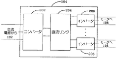
図1Aおよび1Bは、システム構成を全体的に示す。交流電源102は、可変速駆動装置(VSD)104に供給し、VSD104は、1つのモータ106(図1A参照)または複数のモータ106(図1B参照)に電力供給する。モータ(複数可)106を使用して、冷却または冷却器システム(全体は図3参照)の対応する圧縮器を駆動することが好ましい。交流電源102は、単相または多相(たとえば、3相)で、定電圧、かつ固定周波数の交流電力を、その場所に存在する交流電力網または配電システムからVSD104に供給する。交流電源102は、対応する交流電力網に応じて、200V、230V、380V、460V、または600Vの交流電圧または線間電圧を、50Hzまたは60Hzの線周波数で、VSD104に供給できることが好ましい。
1A and 1B show the overall system configuration. The
VSD104は、特定の固定線間電圧および固定線周波数を有する交流電力を交流電源102から受け取り、かつ所望の電圧および所望の周波数で、モータ(複数可)106に交流電力を供給する。所望の電圧と所望の周波数はどちらも、特定の要件を満たすように変化させることができる。VSD104は、モータ(複数可)106の定格電圧および周波数より高い電圧および周波数ならびにより低い電圧および周波数を有する交流電力を、モータ(複数可)106に供給できることが好ましい。別の実施形態では、VSD104は、モータ(複数可)106の定格電圧および周波数に比べて、この場合もより高い周波数およびより低い周波数を供給できるが、それと同じまたはそれより低い電圧を供給する。モータ(複数可)106は、誘導モータであることが好ましいが、可変速で動作させることが可能な任意のタイプのモータを含むことができる。誘導モータは、2極、4極、または6極を含む任意の適切な極構成を有することができる。
The
図2Aおよび2Bは、VSD104の異なる実施形態を示す。VSD104は、コンバータ段202、直流リンク段204、および1つのインバータ206(図2A参照)または複数のインバータ206(図2B参照)を有する出力段という3つの段を有することができる。コンバータ202は、交流電源102からの固定線周波数、固定線間電圧の交流電力を、直流電力に変換する。直流リンク204は、コンバータ202からの直流電力をフィルタリングし、かつエネルギー蓄積構成要素を提供する。直流リンク204は、高い信頼率および非常に低い故障率を示す受動デバイスであるコンデンサ、インダクタ、またはそれらの組合せから構成することができる。最後に、図2Aの実施形態では、インバータ206は、直流リンク204からの直流電力を、モータ106のための可変周波数、可変電圧の交流電力に変換し、また図2Bの実施形態では、複数のインバータ206は、直流リンク204上で並列に接続され、各インバータ206は、直流リンク204からの直流電力を、対応するモータ106のための可変周波数、可変電圧の交流電力に変換する。インバータ(複数可)206は、ワイアボンド技術で相互接続された電力トランジスタと、絶縁ゲートバイポーラトランジスタ(IGBT)電力スイッチと、逆ダイオードとを含むことができる電力モジュールとすることができる。さらに、VSD104の直流リンク204およびインバータ(複数可)206が適切な出力電圧および周波数をモータ106に供給することができる限り、VSD104の直流リンク204およびインバータ(複数可)206は、上に論じた構成要素とは異なる構成要素を組み込むことができることを理解されたい。
2A and 2B show different embodiments of the
図1Bおよび2Bに関しては、複数のインバータ206は、インバータ206それぞれに供給される共通の制御信号または制御命令に基づいて、各インバータ206が同じ所望の電圧および周波数で対応するモータに交流電力を供給するように、制御システムによって共同で制御される。別の実施形態では、複数のインバータ206は、各インバータ206に供給される別個の制御信号または制御命令に基づいて、各インバータ206が異なる所望の電圧および周波数で対応するモータ106に交流電力を供給できるように、制御システムによって個別に制御される。この特性により、VSD104の複数のインバータ206は、他のインバータ206に接続された他のモータ106およびシステムの要件にかかわらず、より効果的に、モータ106およびシステムの要求および負荷を満たすことができる。たとえば、あるインバータ206は、別のインバータ206が別のモータ106に電力の2分の1を供給している間に、全電力をモータ106に供給している可能性がある。複数のインバータ206の制御は、どちらの実施形態でも、制御パネルまたは他の適切な制御デバイスによって行うことができる。
With respect to FIGS. 1B and 2B, a plurality of
各モータ106がVSD104によって電力供給されるように、VSD104の出力段には対応するインバータ206が存在する。VSD104によって電力供給できるモータ106の数は、VSD104内に組み込まれたインバータ206の数に依存する。一実施形態では、直流リンク204と並列に接続され、かつ対応するモータ106に電力供給するために使用される2つまたは3ついずれかのインバータ206を、VSD104内に組み込むことができる。VSD104は、2つと3つの間のインバータ206を有することができるが、直流リンク204がインバータ206それぞれに適切な直流電圧を供給しかつそれを維持できる限り、4つ以上のインバータ206を使用できることを理解されたい。
There is a
図3は、図1Aおよび2Aのシステム構成およびVSD104を使用する冷却または冷却器システムの一実施形態を全体的に示す。図3に示すように、HVAC、冷却、または液体冷却器システム300は、圧縮器302と、凝縮器構成304と、液体冷却器または蒸発器構成306と、制御パネル308とを含む。圧縮器302は、VSD104によって電力供給されるモータ106によって駆動される。VSD104は、特定の固定線間電圧および固定線周波数を有する交流電力を交流電源102から受け取り、かつ所望の電圧および所望の周波数で、モータ106に交流電力を供給する。所望の電圧と所望の周波数はどちらも、特定の要件を満たすように変化させることができる。制御パネル308は、冷却システム300の動作を制御するために、アナログ−デジタル(A/D)コンバータ、マイクロプロセッサ、不揮発性メモリ、およびインターフェース基板などの様々な異なる構成要素を含むことができる。また、制御パネル308を使用して、VSD104およびモータ106の動作を制御することもできる。
FIG. 3 generally illustrates one embodiment of a cooling or chiller system using the system configuration and
圧縮器302は、冷媒蒸気を圧縮し、かつ吐出ラインを通ってこの蒸気を凝縮器304へ送る。圧縮器302は、任意の適切なタイプの圧縮器、たとえばスクリュー圧縮器、遠心圧縮器、往復動圧縮器、スクロール圧縮器とすることができる。圧縮器302によって凝縮器304へ送られる冷媒蒸気は、流体、たとえば空気または水との熱交換関係に入り、かつ流体との熱交換関係の結果、冷媒液への相転移を受ける。凝縮器304からの凝縮された液体の冷媒は、膨張デバイス(図示せず)を通って蒸発器306へ流れる。
The
蒸発器306は、冷却負荷の供給ラインおよび戻りラインのための接続を含むことができる。二次液、たとえば水、エチレン、塩化カルシウムブライン、または塩化ナトリウムブラインが、戻りラインを介して蒸発器306内へ移動し、かつ供給ラインを介して蒸発器306を出る。蒸発器306内の液体の冷媒は、二次液との熱交換関係に入って、二次液の温度を下げる。蒸発器306内の冷媒液は、二次液との熱交換関係の結果、冷媒蒸気への相転移を受ける。蒸発器306内の蒸気の冷媒は、蒸発器306を出て、吸込ラインによって圧縮器302に戻り、サイクルを完成する。凝縮器304および蒸発器306内で冷媒の適切な相転移が得られることを条件として、任意の適切な構成の凝縮器304および蒸発器306をシステム300内で使用できることを理解されたい。
The
HVAC、冷却、または液体冷却器システム300は、図3に図示しない多くの他の特徴を含むことができる。これらの特徴は、説明を簡単にするために図面を簡略化する目的で意図的に省略した。さらに、図3は、HVAC、冷却、または液体冷却器システム300を、単一の冷媒回路内に接続された1つの圧縮器を有するものとして示すが、システム300は、図1Bおよび2Bに示すように単一のVSDによって電力供給され、または1つもしくは複数の冷媒回路それぞれに接続された複数のVSD(全体は図1Aおよび2Aに示す実施形態参照)によって電力供給される、複数の圧縮器を有することができることを理解されたい。
The HVAC, cooling, or liquid
次に図4を参照すると、入力フィルタ10の素子の概略図を示す。アクティブコンバータ202によって生成されるEMI/RFI源は、3相交流入力インダクタ16を位相ごとに線側インダクタ26と負荷側インダクタ28とに分割することによって、コンバータ202より前方でフィルタリングされる。線側インダクタ26と負荷側インダクタ28は、インダクタタップ部分18によって接続される。容量性3相フィルタ素子20は、インダクタタップ部分18間でY接続される。任意選択の接地接続22を、Y接続されたフィルタ素子20の共通点21に接続することができる。別法として、接地接続22は、接地コンデンサ23を含むことができる。線側インダクタ26および負荷側インダクタ28、ならびに容量性フィルタ素子20は、EMI/RFI源、すなわちコンバータ202によって伝導される入力電流の高周波スイッチング成分の減衰をもたらすようなインダクタンスおよび静電容量値で設計される。入力フィルタは、インダクタンス26および28の微分モード誘導成分を介して高インピーダンスを提供し、かつEMI/RFI源への3相Y接続された静電容量20を介して低インピーダンスを提供しながら、電力電流の基本成分、たとえば60Hzには、最小のインピーダンスでネットワークを通過させる。4脚または5脚(4/5)入力インダクタ16を利用することによって、インダクタンス26および28を介してコモンモード誘導成分が形成され、任意選択の接地接続22または接地コンデンサ23とともにフィルタ10の容量まで増大し、かつコンバータ202によって生成されるコモンモード電流が電源102内に流れるのを防止するように作用する。入力フィルタ10のY接続点21は、直接接地させることができ、または別法として、より多くの高周波電流を接地へ分流するために、別個のコンデンサ23を通って接地させることもできる。一実施形態では、インダクタ16には、低い巻線間静電容量を与えることができる。
Referring now to FIG. 4, a schematic diagram of the elements of the
線側インダクタ26は、Y接続されたコンデンサ20と交流電源102との間に、VSD104の所定のスイッチング周波数でインピーダンスを与える。線側インダクタ26のインピーダンスは、入力交流電源102とVSD104との間に大きなインピーダンスをもたないシステムより、Y接続されたコンデンサ20を効果的にすることができるように設計される。インダクタ26はまた、逆方向に高周波インピーダンスを与えて、コンバータ202から交流電源102への高周波電流の流れを制約する。したがってインダクタ26は、高周波放射が元の交流電源102に反射するのを制約または制限する。
The line-
インダクタ28は、コンデンサ20とVSD104への入力との間にインピーダンスを与える。インダクタ28は、交流電源102とVSD104のアクティブコンバータ202部分との間に高インピーダンスを与える。別法として、VSD104が受動整流器コンバータを有する従来のVSDである場合、インダクタ28のインピーダンスは、VSD104を入力交流電源102から分離し、かつVSD104から電源102へ伝導される高周波放射を低減させる。
Y接続されたコンデンサバンク20は、VSD104の少なくとも1つのスイッチング周波数に対して相導体A、B、およびCの間に低インピーダンスを与え、かつ微分モード電流の流れに対して低インピーダンスを与える。Y接続されたコンデンサバンク20はまた、接地接続が供給されるものとすると、コモンモード電流の流れを低減させるために、少なくとも1つのスイッチング周波数の流れに対して接地接続22への低インピーダンス経路を提供する。
Y-connected
次に図5および6を参照すると、一実施形態では、コモンモード入力フィルタ10は、アクティブコンバータ技術を有するVSD104の入力に適用される4脚交流インダクタ516’(たとえば、図8、プライム符号で指定した4脚インダクタの実施形態参照)または5脚交流インダクタ516(集合的に4/5インダクタと呼ぶ)のいずれかを使用して、実施することができる。従来のフィルタは、3脚インダクタを使用して、力率および高調波入力電流の制御を提供する。4/5インダクタ516は、コモンモードと微分モードの両方のインダクタンスを提供する。図5および6は、3相電力システムにおいてさらなる幾何学的対称性を提供する5脚インダクタ516を示す。コモンモードインダクタンスは、矢印502で示す磁束経路504を提供することによって生成される。磁束経路504は、それぞれ3相入力電力102の位相のうちの1つに接続された3つのコア脚部510、512、および514と磁気的に連通する。磁束経路は、内側の3つのコア脚部510、512、および514を囲む連続した磁気透過性の磁気ループである。コア脚部510、512、および514はそれぞれ、それぞれのコア脚部510、512、および514の実質上表面積全体に巻き付けたコイル巻線または導体26(たとえば、図4参照)を有する。磁束経路内の磁束の方向は、コイル巻線内の電流の方向および大きさに依存し、したがって、実際には磁束はインダクタ516の周囲の周りを一方の方向または別の方向に流れる可能性があるが、どちらの方向にも流れるものとして示す。コモンモードの磁束は、3つのインダクタコイル16すべてに共通の電流によって誘導される。この共通の磁束経路504は、インダクタコイルの中を流れるコモンモード電流成分によってのみ励磁させることができる。そのようなインダクタの断面の絵画図を、図5に示す。このインダクタ516は、熱放散を改善しかつインダクタ516の電力容量を増大させるための液体冷却されたコアを有する。
Referring now to FIGS. 5 and 6, in one embodiment, the common
図6を参照すると、5脚インダクタ516の正面断面図は、コア飽和を防止しかつインダクタ516の作用する磁束密度範囲を増大させるために脚部510、512、および514内に挿入された空隙520を示す。インダクタ516では、空隙520は、磁束経路504の水平部間に配置される。また、コア脚部510、512、および514それぞれの中間に2つの空隙520が挿入されて、各コア脚部510、512、および514を3つの個別の部分に分割する。他の空隙構成を使用して、同じ結果を実現することもできる。
Referring to FIG. 6, a front cross-sectional view of a five-
次に図7を参照すると、コモンモード/微分モード入力フィルタ回路とともに出力フィルタを有する可変速駆動装置の一実施形態を示す。図4に関連して前述したEMI/RFI入力フィルタが、コンバータ202の入力で接続され、前述のものと同じフィルタリング機能を実行する。VSD104への入力でインダクタ16を有する入力フィルタを追加することで、交流電力電源102とVSD104との間に高インピーダンス回路を効果的に提供する。コモンモード電流の流れに対して低インピーダンス経路を提供するように、3つのコモンモードコンデンサ32を含む3相Y接続されたコンデンサバンク30が、VSDのモータ接続端子38と接地22との間に接続される。コンデンサバンク30は、高周波数での短絡、すなわち低インピーダンスと同等であり、3つのVSD出力端子34上に存在する破壊的な高周波交流成分を効果的に接地し、かつ破壊的な交流成分が、VSDに接続されたモータまたは他のタイプの負荷に到達しないように分流し、したがってコモンモード電圧から生じる電流をフィルタリング除去する。コンデンサバンク30により、高周波交流成分をモータの寄生容量性接地素子へバイパスさせることができ、コモンモード電圧および電流によって生じるベアリング損傷をなくす。
Referring now to FIG. 7, one embodiment of a variable speed drive apparatus having an output filter with a common mode / differential mode input filter circuit is shown. The EMI / RFI input filter described above in connection with FIG. 4 is connected at the input of
インバータ出力端子34は、システム負荷、たとえばモータ106に接続された出力端子38と直列に接続された3相インダクタ36を含む第2のフィルタ構成に供給する。第2の3相コンデンサバンク42は、3相インダクタ36の負荷側間で出力電力位相L1、L2、およびL3にY接続され、微分モード電流をコンデンサバンク42の中へ流すための低インピーダンス経路を提供する。3相インダクタ36の負荷側にY接続された第2の3相コンデンサバンクを組み合わせることにより、L−C微分モード出力フィルタを提供する。コモンモードフィルタコンデンサバンク30を、L−C微分モードインダクタ36およびコンデンサバンク42と組み合わせることによって、両方の破壊的条件、すなわちコモンモードおよび微分モード電流が、VSD104によって電力供給される負荷に到達するのを防止する。
The
図に示しかつ本明細書に説明した例示的な実施形態は、現在好ましいが、これらの実施形態は例示のみを目的として提供されることを理解されたい。したがって、本出願は、特定の実施形態に限定されるものではなく、やはり添付の特許請求の範囲の範囲内に入る様々な修正形態に及ぶ。あらゆる工程または方法ステップの順番または順序は、代替実施形態によって変更しまたは並べなおすことができる。 While the exemplary embodiments shown in the figures and described herein are presently preferred, it should be understood that these embodiments are provided for illustrative purposes only. Accordingly, the present application is not limited to a particular embodiment, but extends to various modifications that still fall within the scope of the appended claims. The order or sequence of any process or method steps can be changed or re-sequenced according to alternative embodiments.
様々な例示的な実施形態に示す可変速駆動装置用のコモンモードおよび微分モードフィルタの構造および構成は、例示にすぎないことに留意することが重要である。本開示では、2、3の実施形態のみについて詳細に説明してきたが、特許請求の範囲に記載の主題の新規な教示および利点から実質的に逸脱することなく、多くの修正形態(たとえば、様々な要素のサイズ、寸法、構造、形状、および割合、パラメータの値、取付け構成、材料の使用法、色、向きなどの変形形態)が可能であることが、本開示を検討する当業者であれば容易に理解されるであろう。たとえば、一体形成されるものとして示す要素を複数の部分または要素から構築することができ、要素の位置を逆にしまたは他の形で変更することができ、また個別の要素の性質もしくは数または位置を変えまたは変更することができる。したがって、そのような修正形態はすべて、本出願の範囲内に含まれるものとする。あらゆる工程または方法ステップの順番または順序は、代替実施形態によって変更しまたは並べなおすことができる。特許請求の範囲では、あらゆるミーンズ−プラス−ファンクション節は、記載の機能を実行するものとして本明細書に説明した構造を包含し、かつ構造上の等価物だけでなく同等の構造も包含するものとする。本出願の範囲から逸脱することなく、他の置換え、修正、変更、および省略を、例示的な実施形態の設計、動作条件、および構成に加えることができる。 It is important to note that the structure and configuration of common mode and differential mode filters for variable speed drives shown in the various exemplary embodiments is exemplary only. Although only a few embodiments have been described in detail in this disclosure, many modifications (e.g., various types) have been described without substantially departing from the novel teachings and advantages of the claimed subject matter. Anyone skilled in the art reviewing this disclosure will be able to modify the size, dimensions, structure, shape, and proportions of various elements, parameter values, mounting configurations, material usage, color, orientation, etc. Will be easily understood. For example, an element shown as being integrally formed can be constructed from multiple parts or elements, the position of elements can be reversed or otherwise changed, and the nature or number or position of individual elements Can be changed or changed. Accordingly, all such modifications are intended to be included within the scope of this application. The order or sequence of any process or method steps can be changed or re-sequenced according to alternative embodiments. In the claims, every means-plus-function section includes the structures described herein as performing the described functions, and includes not only structural equivalents, but also equivalent structures. And Other substitutions, modifications, changes, and omissions may be made to the design, operating conditions, and configuration of the exemplary embodiments without departing from the scope of this application.
Claims (22)
前記交流入力電圧を供給する交流電源に接続され、前記交流入力電圧をブースト直流電圧に変換するように構成された、コンバータ段と、
前記コンバータ段に接続され、前記コンバータ段からの前記ブースト直流電圧をフィルタリングしかつ蓄積するように構成された、直流リンクと、
前記直流リンクに接続され、前記直流リンクからの前記ブースト直流電圧を、前記可変電圧および前記可変周波数を有する前記出力交流電力に変換するように構成された、インバータ段と、
前記コンバータ段の入力で前記可変速駆動システムに接続され、前記交流電源に存在する伝導電磁妨害または無線周波妨害によって誘導されるコモンモード電流成分および微分モード電流成分をフィルタリングするための入力フィルタと、
前記入力フィルタは、
各巻線が各巻線を1対のインダクタ部に分割するセンタタップを有する、3つの巻線をもつ3相インダクタと、
一方の端部で前記3つのセンタタップに、かつ反対端で共通点にY形に接続された3つのコンデンサを有する3相入力コンデンサバンクと、を備え、
前記3相入力コンデンサバンクは、前記所定の基本周波数を前記コンバータ段へ通過させる間に、前記3相コンデンサバンクを通じて所定の基本周波数を超える周波数を分流するための、所定の基本周波数を超える周波数に対する短絡回路を実質的に提供するように構成され、
前記3相インダクタは、少なくとも3つの脚部分を有するコア要素を含む5脚インダクタであり、各前記脚部分は1対の電流を伝えるコイルで巻かれ、前記3つの脚部分を連続した磁気経路に接続する磁束部分であり、前記磁束部分は、実質上方形のフレーム部分を形成するために、上端部で上脚部によって接続されかつ下端部で下脚部によって接続された1対の垂直脚部を有し、前記3つの脚部分は、前記フレーム部分と磁気的に連通し前記フレーム部分内に配置されている、
可変速駆動システム。 A variable speed drive system configured to receive input AC power at a fixed AC input voltage magnitude and frequency and to provide output AC power at a variable voltage and variable frequency,
A converter stage connected to an AC power source for supplying the AC input voltage and configured to convert the AC input voltage to a boost DC voltage;
A DC link connected to the converter stage and configured to filter and store the boost DC voltage from the converter stage;
An inverter stage connected to the DC link and configured to convert the boost DC voltage from the DC link into the output AC power having the variable voltage and the variable frequency;
An input filter connected to the variable speed drive system at the input of the converter stage for filtering common mode and differential mode current components induced by conducted electromagnetic interference or radio frequency interference present in the AC power supply;
The input filter is
A three-phase inductor with three windings, each winding having a center tap that divides each winding into a pair of inductor sections;
A three-phase input capacitor bank having three capacitors connected to the three center taps at one end and in a Y-shape to the common point at the opposite end;
The three-phase input capacitor bank is configured to shunt a frequency exceeding a predetermined fundamental frequency through the three-phase capacitor bank while passing the predetermined fundamental frequency to the converter stage. Configured to substantially provide a short circuit;
The three-phase inductor is a five-leg inductor that includes a core element having at least three leg portions, each leg portion being wound with a coil carrying a pair of currents, and the three leg portions in a continuous magnetic path. A pair of vertical legs connected by an upper leg at an upper end and connected by a lower leg at a lower end to form a substantially upper frame portion. The three leg portions are in magnetic communication with the frame portion and disposed within the frame portion;
Variable speed drive system.
前記第1の出力コンデンサバンクの各前記3つのコンデンサは、前記出力相接続の反対端に共通して接続され、前記共通コンデンサ接続がまた、接地に接続されている、
請求項1に記載の可変速駆動システム。 Each capacitor further comprising a first output capacitor bank consisting of three capacitors connected in Y-shape to the output phase of the inductor;
Each of the three capacitors of the first output capacitor bank is connected in common to the opposite end of the output phase connection, and the common capacitor connection is also connected to ground;
The variable speed drive system according to claim 1.
各コンデンサが、Y形に前記出力インダクタの負荷側に接続されている3つのコンデンサからなる第2の出力コンデンサバンクと、をさらに備え、
微分モード電圧成分によって誘導される電流が、前記出力インダクタの前記負荷側から実質上除去され、かつ前記出力インダクタに接続された負荷へ流れるのを防止する、
請求項6に記載の可変速駆動システム。 An output inductor having three output phase windings connected in series with the output phase of the inverter stage;
Each capacitor further comprises a second output capacitor bank consisting of three capacitors connected in a Y shape to the load side of the output inductor;
Preventing current induced by the differential mode voltage component from being substantially removed from the load side of the output inductor and flowing to a load connected to the output inductor;
The variable speed drive system according to claim 6.
Y形で、一方の端部で前記3つのセンタタップに接続され、かつ反対端で共通点に接続されている3つのコンデンサを有する3相入力コンデンサバンクと、を備え、
前記3相入力コンデンサバンクは、前記所定の基本周波数を入力交流電源へ通過させる間に、前記3相コンデンサバンクを通じて所定の基本周波数を超える周波数を分流するための所定の基本周波数を超える周波数に対して実質上短絡回路を提供するように構成され、
前記3相インダクタは、少なくとも3つの脚部分を有するコア要素を含む5脚インダクタであり、各前記脚部分は1対の電流を伝えるコイルで巻かれ、前記3つの脚部分を連続した磁気経路に接続する磁束部分であり、前記磁束部分は、実質上方形のフレーム部分を形成するために、上端部で上脚部によって接続されかつ下端部で下脚部によって接続された1対の垂直脚部を有し、前記3つの脚部分は、前記フレーム部分と磁気的に連通し前記フレーム部分内に配置されている、
コモンモードおよび微分モード電流をフィルタリングするための入力フィルタ。 A three-phase inductor having three windings, each winding having a center tap that divides each winding into a pair of inductor sections;
A three-phase input capacitor bank having three capacitors in Y form, connected to the three center taps at one end and connected to a common point at the opposite end;
The three-phase input capacitor bank has a frequency exceeding a predetermined basic frequency for diverting a frequency exceeding the predetermined basic frequency through the three-phase capacitor bank while passing the predetermined basic frequency to the input AC power source. Configured to provide a substantially short circuit,
The three-phase inductor is a five-leg inductor that includes a core element having at least three leg portions, each leg portion being wound with a coil carrying a pair of currents, and the three leg portions in a continuous magnetic path. A pair of vertical legs connected by an upper leg at an upper end and connected by a lower leg at a lower end to form a substantially upper frame portion. The three leg portions are in magnetic communication with the frame portion and disposed within the frame portion;
Input filter for filtering common mode and differential mode currents.
前記圧縮器に電力供給するように前記圧縮器に接続されたモータと、
前記モータに接続され、固定の交流入力電圧の大きさおよび周波数で入力交流電力を受け取り、かつ可変電圧および可変周波数で出力交流電力を供給するように構成されている可変速駆動装置とを備え、前記可変速駆動装置は、
前記交流入力電圧を供給する交流電源に接続され、前記交流入力電圧をブースト直流電圧に変換するように構成されているコンバータ段と、
前記コンバータ段に接続され、前記コンバータ段からの前記ブースト直流電圧をフィルタリングしかつ蓄積するように構成されている直流リンクと、
前記直流リンクに接続され、前記直流リンクからの前記ブースト直流電圧を、前記可変電圧および前記可変周波数を有する前記出力交流電力に変換するように構成されているインバータ段と、
コモンモードおよび微分モード電流をフィルタリングするための入力フィルタと、を備え、
前記入力フィルタは、
各巻線は各巻線を1対のインダクタ部に分割するセンタタップを有する、3つの巻線を有する3相インダクタと、
Y形で、一方の端部で前記3つのセンタタップに接続され、かつ反対端で共通点に接続されている、3つのコンデンサを有する3相入力コンデンサバンクと、を備え、
前記3相入力コンデンサバンクは、前記所定の基本周波数を前記コンバータ段へ通過させる間に、前記3相コンデンサバンクを通じて所定の基本周波数を超える周波数を分流するための所定の基本周波数を超える周波数に対して実質上短絡回路を提供するように構成され、
前記3相インダクタは、少なくとも3つの脚部分を有するコア要素を含む5脚インダクタであり、各前記脚部分は1対の電流を伝えるコイルで巻かれ、前記3つの脚部分を連続した磁気経路に接続する磁束部分であり、前記磁束部分は、実質上方形のフレーム部分を形成するために、上端部で上脚部によって接続されかつ下端部で下脚部によって接続された1対の垂直脚部を有し、前記3つの脚部分は、前記フレーム部分と磁気的に連通し前記フレーム部分内に配置されている、
冷却器システム。 A refrigerant circuit comprising a compressor, a condenser, and an evaporator connected to a closed refrigerant loop;
A motor connected to the compressor to power the compressor;
A variable speed drive connected to the motor and configured to receive input AC power at a fixed AC input voltage magnitude and frequency and to supply output AC power at a variable voltage and variable frequency; The variable speed drive is
A converter stage connected to an AC power source for supplying the AC input voltage and configured to convert the AC input voltage to a boost DC voltage;
A DC link connected to the converter stage and configured to filter and store the boost DC voltage from the converter stage;
An inverter stage connected to the DC link and configured to convert the boost DC voltage from the DC link to the output AC power having the variable voltage and the variable frequency;
An input filter for filtering common mode and differential mode currents,
The input filter is
Each winding has a three-phase inductor with three windings, with a center tap that divides each winding into a pair of inductor sections;
A three-phase input capacitor bank having three capacitors, Y-shaped, connected to the three center taps at one end and connected to a common point at the opposite end;
The three-phase input capacitor bank is used for a frequency exceeding a predetermined fundamental frequency for diverting a frequency exceeding a predetermined fundamental frequency through the three-phase capacitor bank while passing the predetermined fundamental frequency to the converter stage. Configured to provide a substantially short circuit,
The three-phase inductor is a five-leg inductor that includes a core element having at least three leg portions, each leg portion being wound with a coil carrying a pair of currents, and the three leg portions in a continuous magnetic path. A pair of vertical legs connected by an upper leg at an upper end and connected by a lower leg at a lower end to form a substantially upper frame portion. The three leg portions are in magnetic communication with the frame portion and disposed within the frame portion;
Chiller system.
各コンデンサがY形で前記インダクタの出力相に接続されている、3つのコンデンサからなる第1の出力コンデンサバンクを備え、
前記第1の出力コンデンサバンクの各前記3つのコンデンサは、前記出力相接続の反対端で共通して接続され、前記共通のコンデンサ接続はまた、接地に接続される、請求項20に記載の冷却器システム。 An output filter for filtering common mode and differential mode currents associated with the variable speed drive, the output filter comprising:
Comprising a first output capacitor bank of three capacitors, each capacitor being Y-shaped and connected to the output phase of the inductor;
21. The cooling of claim 20 , wherein each of the three capacitors of the first output capacitor bank is connected in common at the opposite end of the output phase connection, and the common capacitor connection is also connected to ground. System.
前記インバータ段の前記出力相と直列に接続された3つの出力相巻線を有する出力インダクタと、
各コンデンサがY形で前記出力インダクタの負荷側に接続されている、3つのコンデンサからなる第2の出力コンデンサバンクと、をさらに備え、
微分モード電圧成分によって誘導される電流が、前記出力インダクタの前記負荷側から実質上除去され、かつ前記出力インダクタに接続された負荷へ流れるのを防止する、請求項21に記載の冷却器システム。 The output filter is
An output inductor having three output phase windings connected in series with the output phase of the inverter stage;
A second output capacitor bank consisting of three capacitors, each capacitor being Y-shaped and connected to the load side of the output inductor,
The cooler system of claim 21 , wherein a current induced by a differential mode voltage component is substantially removed from the load side of the output inductor and prevented from flowing to a load connected to the output inductor.
Applications Claiming Priority (3)
| Application Number | Priority Date | Filing Date | Title |
|---|---|---|---|
| US11/931,993 US7746020B2 (en) | 2007-01-22 | 2007-10-31 | Common mode & differential mode filter for variable speed drive |
| US11/931,993 | 2007-10-31 | ||
| PCT/US2008/052203 WO2008092152A2 (en) | 2007-01-22 | 2008-01-28 | Common mode and differential mode filter for variable speed drive |
Publications (3)
| Publication Number | Publication Date |
|---|---|
| JP2011502457A JP2011502457A (en) | 2011-01-20 |
| JP2011502457A5 JP2011502457A5 (en) | 2011-05-26 |
| JP5443999B2 true JP5443999B2 (en) | 2014-03-19 |
Family
ID=42751670
Family Applications (1)
| Application Number | Title | Priority Date | Filing Date |
|---|---|---|---|
| JP2009546584A Active JP5443999B2 (en) | 2007-10-31 | 2008-01-28 | Common mode and differential mode filters for variable speed drives |
Country Status (2)
| Country | Link |
|---|---|
| JP (1) | JP5443999B2 (en) |
| KR (1) | KR101265738B1 (en) |
Families Citing this family (4)
| Publication number | Priority date | Publication date | Assignee | Title |
|---|---|---|---|---|
| KR20120060271A (en) * | 2010-12-01 | 2012-06-12 | 한국전기연구원 | Inverter parallel operation using current balancer in wind power generation system |
| KR102061066B1 (en) | 2014-12-09 | 2020-02-11 | 존슨 컨트롤스 테크놀러지 컴퍼니 | Electromagnetic Compatibility Filter |
| WO2016182911A1 (en) * | 2015-05-08 | 2016-11-17 | Johnson Controls Technology Company | Variable speed drive with active converter |
| CN109792214B (en) | 2016-10-05 | 2021-03-19 | 江森自控科技公司 | Variable speed drive with secondary winding |
Family Cites Families (8)
| Publication number | Priority date | Publication date | Assignee | Title |
|---|---|---|---|---|
| JP3596694B2 (en) * | 1995-09-19 | 2004-12-02 | 株式会社安川電機 | Filter circuit for PWM inverter |
| JP4209100B2 (en) * | 2001-09-13 | 2009-01-14 | 三菱電機株式会社 | Noise reduction device for power converter |
| JP2003169495A (en) * | 2001-11-30 | 2003-06-13 | Nippon Reliance Kk | Ac variable speed driver |
| JP3780949B2 (en) * | 2002-01-21 | 2006-05-31 | 株式会社日立製作所 | Power converter |
| US6850426B2 (en) * | 2002-04-30 | 2005-02-01 | Honeywell International Inc. | Synchronous and bi-directional variable frequency power conversion systems |
| JP2004364492A (en) * | 2003-05-09 | 2004-12-24 | Sanyo Electric Co Ltd | Motor-driving device and air-conditioning equipment |
| DE102005005688A1 (en) * | 2005-02-08 | 2006-08-10 | Siemens Ag | Filter for backfeedable rectifier, has capacitor connected at each connection point of winding portions, which are arranged on common core in such a manner that their ampere turns mutually compensate during flow |
| JP4404029B2 (en) * | 2005-08-09 | 2010-01-27 | 三菱電機株式会社 | Noise filter |
-
2008
- 2008-01-28 JP JP2009546584A patent/JP5443999B2/en active Active
- 2008-01-28 KR KR1020097014775A patent/KR101265738B1/en active IP Right Grant
Also Published As
| Publication number | Publication date |
|---|---|
| KR20100075773A (en) | 2010-07-05 |
| KR101265738B1 (en) | 2013-05-21 |
| JP2011502457A (en) | 2011-01-20 |
Similar Documents
| Publication | Publication Date | Title |
|---|---|---|
| US7746020B2 (en) | Common mode & differential mode filter for variable speed drive | |
| JP6738456B2 (en) | Electromagnetic compatibility filter | |
| JP6212571B2 (en) | Hybrid pulse width modulation method for variable speed drive | |
| US8174853B2 (en) | Variable speed drive | |
| US7957166B2 (en) | Variable speed drive | |
| US7724549B2 (en) | Integrated power conditioning system and housing for delivering operational power to a motor | |
| JP5308474B2 (en) | Refrigeration equipment | |
| US10530239B2 (en) | Filter systems for reducing bearing current in high-frequency motor control systems | |
| JP5443999B2 (en) | Common mode and differential mode filters for variable speed drives | |
| Wu et al. | An integrated DC link choke for elimination of motor common-mode voltage in medium voltage drives | |
| US11512885B2 (en) | Variable speed drive with secondary windings | |
| JP2012124985A (en) | Refrigeration apparatus | |
| JP2011502457A5 (en) | ||
| CN114208007B (en) | Circuit body and refrigeration cycle device |
Legal Events
| Date | Code | Title | Description |
|---|---|---|---|
| A521 | Request for written amendment filed |
Free format text: JAPANESE INTERMEDIATE CODE: A523 Effective date: 20110406 |
|
| A131 | Notification of reasons for refusal |
Free format text: JAPANESE INTERMEDIATE CODE: A131 Effective date: 20120912 |
|
| A521 | Request for written amendment filed |
Free format text: JAPANESE INTERMEDIATE CODE: A523 Effective date: 20121212 |
|
| A131 | Notification of reasons for refusal |
Free format text: JAPANESE INTERMEDIATE CODE: A131 Effective date: 20130627 |
|
| A601 | Written request for extension of time |
Free format text: JAPANESE INTERMEDIATE CODE: A601 Effective date: 20130927 |
|
| A602 | Written permission of extension of time |
Free format text: JAPANESE INTERMEDIATE CODE: A602 Effective date: 20131004 |
|
| A521 | Request for written amendment filed |
Free format text: JAPANESE INTERMEDIATE CODE: A523 Effective date: 20131018 |
|
| TRDD | Decision of grant or rejection written | ||
| A01 | Written decision to grant a patent or to grant a registration (utility model) |
Free format text: JAPANESE INTERMEDIATE CODE: A01 Effective date: 20131121 |
|
| A61 | First payment of annual fees (during grant procedure) |
Free format text: JAPANESE INTERMEDIATE CODE: A61 Effective date: 20131220 |
|
| R150 | Certificate of patent or registration of utility model |
Ref document number: 5443999 Country of ref document: JP Free format text: JAPANESE INTERMEDIATE CODE: R150 Free format text: JAPANESE INTERMEDIATE CODE: R150 |
|
| R250 | Receipt of annual fees |
Free format text: JAPANESE INTERMEDIATE CODE: R250 |
|
| R250 | Receipt of annual fees |
Free format text: JAPANESE INTERMEDIATE CODE: R250 |
|
| R250 | Receipt of annual fees |
Free format text: JAPANESE INTERMEDIATE CODE: R250 |
|
| R250 | Receipt of annual fees |
Free format text: JAPANESE INTERMEDIATE CODE: R250 |
|
| R250 | Receipt of annual fees |
Free format text: JAPANESE INTERMEDIATE CODE: R250 |
|
| R250 | Receipt of annual fees |
Free format text: JAPANESE INTERMEDIATE CODE: R250 |
|
| R250 | Receipt of annual fees |
Free format text: JAPANESE INTERMEDIATE CODE: R250 |
|
| R250 | Receipt of annual fees |
Free format text: JAPANESE INTERMEDIATE CODE: R250 |