JP5380376B2 - Power semiconductor device - Google Patents
Power semiconductor device Download PDFInfo
- Publication number
- JP5380376B2 JP5380376B2 JP2010140723A JP2010140723A JP5380376B2 JP 5380376 B2 JP5380376 B2 JP 5380376B2 JP 2010140723 A JP2010140723 A JP 2010140723A JP 2010140723 A JP2010140723 A JP 2010140723A JP 5380376 B2 JP5380376 B2 JP 5380376B2
- Authority
- JP
- Japan
- Prior art keywords
- connection terminal
- power semiconductor
- terminal
- power
- wiring
- Prior art date
- Legal status (The legal status is an assumption and is not a legal conclusion. Google has not performed a legal analysis and makes no representation as to the accuracy of the status listed.)
- Active
Links
Images


Classifications
-
- H—ELECTRICITY
- H05—ELECTRIC TECHNIQUES NOT OTHERWISE PROVIDED FOR
- H05K—PRINTED CIRCUITS; CASINGS OR CONSTRUCTIONAL DETAILS OF ELECTRIC APPARATUS; MANUFACTURE OF ASSEMBLAGES OF ELECTRICAL COMPONENTS
- H05K5/00—Casings, cabinets or drawers for electric apparatus
- H05K5/02—Details
- H05K5/0247—Electrical details of casings, e.g. terminals, passages for cables or wiring
-
- H—ELECTRICITY
- H01—ELECTRIC ELEMENTS
- H01L—SEMICONDUCTOR DEVICES NOT COVERED BY CLASS H10
- H01L23/00—Details of semiconductor or other solid state devices
- H01L23/34—Arrangements for cooling, heating, ventilating or temperature compensation ; Temperature sensing arrangements
- H01L23/46—Arrangements for cooling, heating, ventilating or temperature compensation ; Temperature sensing arrangements involving the transfer of heat by flowing fluids
- H01L23/473—Arrangements for cooling, heating, ventilating or temperature compensation ; Temperature sensing arrangements involving the transfer of heat by flowing fluids by flowing liquids
-
- H—ELECTRICITY
- H01—ELECTRIC ELEMENTS
- H01L—SEMICONDUCTOR DEVICES NOT COVERED BY CLASS H10
- H01L23/00—Details of semiconductor or other solid state devices
- H01L23/48—Arrangements for conducting electric current to or from the solid state body in operation, e.g. leads, terminal arrangements ; Selection of materials therefor
- H01L23/488—Arrangements for conducting electric current to or from the solid state body in operation, e.g. leads, terminal arrangements ; Selection of materials therefor consisting of soldered or bonded constructions
- H01L23/495—Lead-frames or other flat leads
- H01L23/49541—Geometry of the lead-frame
- H01L23/49562—Geometry of the lead-frame for devices being provided for in H01L29/00
-
- H—ELECTRICITY
- H01—ELECTRIC ELEMENTS
- H01L—SEMICONDUCTOR DEVICES NOT COVERED BY CLASS H10
- H01L23/00—Details of semiconductor or other solid state devices
- H01L23/48—Arrangements for conducting electric current to or from the solid state body in operation, e.g. leads, terminal arrangements ; Selection of materials therefor
- H01L23/488—Arrangements for conducting electric current to or from the solid state body in operation, e.g. leads, terminal arrangements ; Selection of materials therefor consisting of soldered or bonded constructions
- H01L23/495—Lead-frames or other flat leads
- H01L23/49575—Assemblies of semiconductor devices on lead frames
-
- H—ELECTRICITY
- H01—ELECTRIC ELEMENTS
- H01L—SEMICONDUCTOR DEVICES NOT COVERED BY CLASS H10
- H01L24/00—Arrangements for connecting or disconnecting semiconductor or solid-state bodies; Methods or apparatus related thereto
- H01L24/01—Means for bonding being attached to, or being formed on, the surface to be connected, e.g. chip-to-package, die-attach, "first-level" interconnects; Manufacturing methods related thereto
- H01L24/34—Strap connectors, e.g. copper straps for grounding power devices; Manufacturing methods related thereto
- H01L24/36—Structure, shape, material or disposition of the strap connectors prior to the connecting process
-
- H—ELECTRICITY
- H01—ELECTRIC ELEMENTS
- H01L—SEMICONDUCTOR DEVICES NOT COVERED BY CLASS H10
- H01L24/00—Arrangements for connecting or disconnecting semiconductor or solid-state bodies; Methods or apparatus related thereto
- H01L24/01—Means for bonding being attached to, or being formed on, the surface to be connected, e.g. chip-to-package, die-attach, "first-level" interconnects; Manufacturing methods related thereto
- H01L24/34—Strap connectors, e.g. copper straps for grounding power devices; Manufacturing methods related thereto
- H01L24/39—Structure, shape, material or disposition of the strap connectors after the connecting process
- H01L24/40—Structure, shape, material or disposition of the strap connectors after the connecting process of an individual strap connector
-
- H—ELECTRICITY
- H01—ELECTRIC ELEMENTS
- H01L—SEMICONDUCTOR DEVICES NOT COVERED BY CLASS H10
- H01L24/00—Arrangements for connecting or disconnecting semiconductor or solid-state bodies; Methods or apparatus related thereto
- H01L24/73—Means for bonding being of different types provided for in two or more of groups H01L24/10, H01L24/18, H01L24/26, H01L24/34, H01L24/42, H01L24/50, H01L24/63, H01L24/71
-
- H—ELECTRICITY
- H02—GENERATION; CONVERSION OR DISTRIBUTION OF ELECTRIC POWER
- H02M—APPARATUS FOR CONVERSION BETWEEN AC AND AC, BETWEEN AC AND DC, OR BETWEEN DC AND DC, AND FOR USE WITH MAINS OR SIMILAR POWER SUPPLY SYSTEMS; CONVERSION OF DC OR AC INPUT POWER INTO SURGE OUTPUT POWER; CONTROL OR REGULATION THEREOF
- H02M7/00—Conversion of ac power input into dc power output; Conversion of dc power input into ac power output
- H02M7/42—Conversion of dc power input into ac power output without possibility of reversal
- H02M7/44—Conversion of dc power input into ac power output without possibility of reversal by static converters
- H02M7/48—Conversion of dc power input into ac power output without possibility of reversal by static converters using discharge tubes with control electrode or semiconductor devices with control electrode
- H02M7/53—Conversion of dc power input into ac power output without possibility of reversal by static converters using discharge tubes with control electrode or semiconductor devices with control electrode using devices of a triode or transistor type requiring continuous application of a control signal
- H02M7/537—Conversion of dc power input into ac power output without possibility of reversal by static converters using discharge tubes with control electrode or semiconductor devices with control electrode using devices of a triode or transistor type requiring continuous application of a control signal using semiconductor devices only, e.g. single switched pulse inverters
-
- H—ELECTRICITY
- H05—ELECTRIC TECHNIQUES NOT OTHERWISE PROVIDED FOR
- H05K—PRINTED CIRCUITS; CASINGS OR CONSTRUCTIONAL DETAILS OF ELECTRIC APPARATUS; MANUFACTURE OF ASSEMBLAGES OF ELECTRICAL COMPONENTS
- H05K7/00—Constructional details common to different types of electric apparatus
- H05K7/14—Mounting supporting structure in casing or on frame or rack
- H05K7/1422—Printed circuit boards receptacles, e.g. stacked structures, electronic circuit modules or box like frames
- H05K7/1427—Housings
- H05K7/1432—Housings specially adapted for power drive units or power converters
- H05K7/14322—Housings specially adapted for power drive units or power converters wherein the control and power circuits of a power converter are arranged within the same casing
-
- H—ELECTRICITY
- H05—ELECTRIC TECHNIQUES NOT OTHERWISE PROVIDED FOR
- H05K—PRINTED CIRCUITS; CASINGS OR CONSTRUCTIONAL DETAILS OF ELECTRIC APPARATUS; MANUFACTURE OF ASSEMBLAGES OF ELECTRICAL COMPONENTS
- H05K7/00—Constructional details common to different types of electric apparatus
- H05K7/20—Modifications to facilitate cooling, ventilating, or heating
- H05K7/20845—Modifications to facilitate cooling, ventilating, or heating for automotive electronic casings
-
- H—ELECTRICITY
- H05—ELECTRIC TECHNIQUES NOT OTHERWISE PROVIDED FOR
- H05K—PRINTED CIRCUITS; CASINGS OR CONSTRUCTIONAL DETAILS OF ELECTRIC APPARATUS; MANUFACTURE OF ASSEMBLAGES OF ELECTRICAL COMPONENTS
- H05K7/00—Constructional details common to different types of electric apparatus
- H05K7/20—Modifications to facilitate cooling, ventilating, or heating
- H05K7/2089—Modifications to facilitate cooling, ventilating, or heating for power electronics, e.g. for inverters for controlling motor
- H05K7/20927—Liquid coolant without phase change
-
- H—ELECTRICITY
- H01—ELECTRIC ELEMENTS
- H01L—SEMICONDUCTOR DEVICES NOT COVERED BY CLASS H10
- H01L21/00—Processes or apparatus adapted for the manufacture or treatment of semiconductor or solid state devices or of parts thereof
- H01L21/02—Manufacture or treatment of semiconductor devices or of parts thereof
- H01L21/04—Manufacture or treatment of semiconductor devices or of parts thereof the devices having at least one potential-jump barrier or surface barrier, e.g. PN junction, depletion layer or carrier concentration layer
- H01L21/50—Assembly of semiconductor devices using processes or apparatus not provided for in a single one of the subgroups H01L21/06 - H01L21/326, e.g. sealing of a cap to a base of a container
- H01L21/56—Encapsulations, e.g. encapsulation layers, coatings
- H01L21/565—Moulds
-
- H—ELECTRICITY
- H01—ELECTRIC ELEMENTS
- H01L—SEMICONDUCTOR DEVICES NOT COVERED BY CLASS H10
- H01L2224/00—Indexing scheme for arrangements for connecting or disconnecting semiconductor or solid-state bodies and methods related thereto as covered by H01L24/00
- H01L2224/01—Means for bonding being attached to, or being formed on, the surface to be connected, e.g. chip-to-package, die-attach, "first-level" interconnects; Manufacturing methods related thereto
- H01L2224/02—Bonding areas; Manufacturing methods related thereto
- H01L2224/04—Structure, shape, material or disposition of the bonding areas prior to the connecting process
- H01L2224/06—Structure, shape, material or disposition of the bonding areas prior to the connecting process of a plurality of bonding areas
- H01L2224/0601—Structure
- H01L2224/0603—Bonding areas having different sizes, e.g. different heights or widths
-
- H—ELECTRICITY
- H01—ELECTRIC ELEMENTS
- H01L—SEMICONDUCTOR DEVICES NOT COVERED BY CLASS H10
- H01L2224/00—Indexing scheme for arrangements for connecting or disconnecting semiconductor or solid-state bodies and methods related thereto as covered by H01L24/00
- H01L2224/01—Means for bonding being attached to, or being formed on, the surface to be connected, e.g. chip-to-package, die-attach, "first-level" interconnects; Manufacturing methods related thereto
- H01L2224/02—Bonding areas; Manufacturing methods related thereto
- H01L2224/04—Structure, shape, material or disposition of the bonding areas prior to the connecting process
- H01L2224/06—Structure, shape, material or disposition of the bonding areas prior to the connecting process of a plurality of bonding areas
- H01L2224/061—Disposition
- H01L2224/0618—Disposition being disposed on at least two different sides of the body, e.g. dual array
- H01L2224/06181—On opposite sides of the body
-
- H—ELECTRICITY
- H01—ELECTRIC ELEMENTS
- H01L—SEMICONDUCTOR DEVICES NOT COVERED BY CLASS H10
- H01L2224/00—Indexing scheme for arrangements for connecting or disconnecting semiconductor or solid-state bodies and methods related thereto as covered by H01L24/00
- H01L2224/01—Means for bonding being attached to, or being formed on, the surface to be connected, e.g. chip-to-package, die-attach, "first-level" interconnects; Manufacturing methods related thereto
- H01L2224/26—Layer connectors, e.g. plate connectors, solder or adhesive layers; Manufacturing methods related thereto
- H01L2224/28—Structure, shape, material or disposition of the layer connectors prior to the connecting process
- H01L2224/29—Structure, shape, material or disposition of the layer connectors prior to the connecting process of an individual layer connector
- H01L2224/29001—Core members of the layer connector
- H01L2224/29099—Material
- H01L2224/291—Material with a principal constituent of the material being a metal or a metalloid, e.g. boron [B], silicon [Si], germanium [Ge], arsenic [As], antimony [Sb], tellurium [Te] and polonium [Po], and alloys thereof
- H01L2224/29138—Material with a principal constituent of the material being a metal or a metalloid, e.g. boron [B], silicon [Si], germanium [Ge], arsenic [As], antimony [Sb], tellurium [Te] and polonium [Po], and alloys thereof the principal constituent melting at a temperature of greater than or equal to 950°C and less than 1550°C
- H01L2224/29139—Silver [Ag] as principal constituent
-
- H—ELECTRICITY
- H01—ELECTRIC ELEMENTS
- H01L—SEMICONDUCTOR DEVICES NOT COVERED BY CLASS H10
- H01L2224/00—Indexing scheme for arrangements for connecting or disconnecting semiconductor or solid-state bodies and methods related thereto as covered by H01L24/00
- H01L2224/01—Means for bonding being attached to, or being formed on, the surface to be connected, e.g. chip-to-package, die-attach, "first-level" interconnects; Manufacturing methods related thereto
- H01L2224/26—Layer connectors, e.g. plate connectors, solder or adhesive layers; Manufacturing methods related thereto
- H01L2224/31—Structure, shape, material or disposition of the layer connectors after the connecting process
- H01L2224/32—Structure, shape, material or disposition of the layer connectors after the connecting process of an individual layer connector
- H01L2224/321—Disposition
- H01L2224/32151—Disposition the layer connector connecting between a semiconductor or solid-state body and an item not being a semiconductor or solid-state body, e.g. chip-to-substrate, chip-to-passive
- H01L2224/32221—Disposition the layer connector connecting between a semiconductor or solid-state body and an item not being a semiconductor or solid-state body, e.g. chip-to-substrate, chip-to-passive the body and the item being stacked
- H01L2224/32225—Disposition the layer connector connecting between a semiconductor or solid-state body and an item not being a semiconductor or solid-state body, e.g. chip-to-substrate, chip-to-passive the body and the item being stacked the item being non-metallic, e.g. insulating substrate with or without metallisation
-
- H—ELECTRICITY
- H01—ELECTRIC ELEMENTS
- H01L—SEMICONDUCTOR DEVICES NOT COVERED BY CLASS H10
- H01L2224/00—Indexing scheme for arrangements for connecting or disconnecting semiconductor or solid-state bodies and methods related thereto as covered by H01L24/00
- H01L2224/01—Means for bonding being attached to, or being formed on, the surface to be connected, e.g. chip-to-package, die-attach, "first-level" interconnects; Manufacturing methods related thereto
- H01L2224/26—Layer connectors, e.g. plate connectors, solder or adhesive layers; Manufacturing methods related thereto
- H01L2224/31—Structure, shape, material or disposition of the layer connectors after the connecting process
- H01L2224/32—Structure, shape, material or disposition of the layer connectors after the connecting process of an individual layer connector
- H01L2224/321—Disposition
- H01L2224/32151—Disposition the layer connector connecting between a semiconductor or solid-state body and an item not being a semiconductor or solid-state body, e.g. chip-to-substrate, chip-to-passive
- H01L2224/32221—Disposition the layer connector connecting between a semiconductor or solid-state body and an item not being a semiconductor or solid-state body, e.g. chip-to-substrate, chip-to-passive the body and the item being stacked
- H01L2224/32245—Disposition the layer connector connecting between a semiconductor or solid-state body and an item not being a semiconductor or solid-state body, e.g. chip-to-substrate, chip-to-passive the body and the item being stacked the item being metallic
-
- H—ELECTRICITY
- H01—ELECTRIC ELEMENTS
- H01L—SEMICONDUCTOR DEVICES NOT COVERED BY CLASS H10
- H01L2224/00—Indexing scheme for arrangements for connecting or disconnecting semiconductor or solid-state bodies and methods related thereto as covered by H01L24/00
- H01L2224/01—Means for bonding being attached to, or being formed on, the surface to be connected, e.g. chip-to-package, die-attach, "first-level" interconnects; Manufacturing methods related thereto
- H01L2224/26—Layer connectors, e.g. plate connectors, solder or adhesive layers; Manufacturing methods related thereto
- H01L2224/31—Structure, shape, material or disposition of the layer connectors after the connecting process
- H01L2224/33—Structure, shape, material or disposition of the layer connectors after the connecting process of a plurality of layer connectors
- H01L2224/331—Disposition
- H01L2224/3318—Disposition being disposed on at least two different sides of the body, e.g. dual array
- H01L2224/33181—On opposite sides of the body
-
- H—ELECTRICITY
- H01—ELECTRIC ELEMENTS
- H01L—SEMICONDUCTOR DEVICES NOT COVERED BY CLASS H10
- H01L2224/00—Indexing scheme for arrangements for connecting or disconnecting semiconductor or solid-state bodies and methods related thereto as covered by H01L24/00
- H01L2224/01—Means for bonding being attached to, or being formed on, the surface to be connected, e.g. chip-to-package, die-attach, "first-level" interconnects; Manufacturing methods related thereto
- H01L2224/34—Strap connectors, e.g. copper straps for grounding power devices; Manufacturing methods related thereto
- H01L2224/39—Structure, shape, material or disposition of the strap connectors after the connecting process
- H01L2224/40—Structure, shape, material or disposition of the strap connectors after the connecting process of an individual strap connector
- H01L2224/401—Disposition
- H01L2224/40135—Connecting between different semiconductor or solid-state bodies, i.e. chip-to-chip
- H01L2224/40137—Connecting between different semiconductor or solid-state bodies, i.e. chip-to-chip the bodies being arranged next to each other, e.g. on a common substrate
-
- H—ELECTRICITY
- H01—ELECTRIC ELEMENTS
- H01L—SEMICONDUCTOR DEVICES NOT COVERED BY CLASS H10
- H01L2224/00—Indexing scheme for arrangements for connecting or disconnecting semiconductor or solid-state bodies and methods related thereto as covered by H01L24/00
- H01L2224/01—Means for bonding being attached to, or being formed on, the surface to be connected, e.g. chip-to-package, die-attach, "first-level" interconnects; Manufacturing methods related thereto
- H01L2224/42—Wire connectors; Manufacturing methods related thereto
- H01L2224/44—Structure, shape, material or disposition of the wire connectors prior to the connecting process
- H01L2224/45—Structure, shape, material or disposition of the wire connectors prior to the connecting process of an individual wire connector
- H01L2224/45001—Core members of the connector
- H01L2224/4501—Shape
- H01L2224/45012—Cross-sectional shape
- H01L2224/45015—Cross-sectional shape being circular
-
- H—ELECTRICITY
- H01—ELECTRIC ELEMENTS
- H01L—SEMICONDUCTOR DEVICES NOT COVERED BY CLASS H10
- H01L2224/00—Indexing scheme for arrangements for connecting or disconnecting semiconductor or solid-state bodies and methods related thereto as covered by H01L24/00
- H01L2224/01—Means for bonding being attached to, or being formed on, the surface to be connected, e.g. chip-to-package, die-attach, "first-level" interconnects; Manufacturing methods related thereto
- H01L2224/42—Wire connectors; Manufacturing methods related thereto
- H01L2224/47—Structure, shape, material or disposition of the wire connectors after the connecting process
- H01L2224/48—Structure, shape, material or disposition of the wire connectors after the connecting process of an individual wire connector
- H01L2224/481—Disposition
- H01L2224/48151—Connecting between a semiconductor or solid-state body and an item not being a semiconductor or solid-state body, e.g. chip-to-substrate, chip-to-passive
- H01L2224/48221—Connecting between a semiconductor or solid-state body and an item not being a semiconductor or solid-state body, e.g. chip-to-substrate, chip-to-passive the body and the item being stacked
- H01L2224/48245—Connecting between a semiconductor or solid-state body and an item not being a semiconductor or solid-state body, e.g. chip-to-substrate, chip-to-passive the body and the item being stacked the item being metallic
- H01L2224/48247—Connecting between a semiconductor or solid-state body and an item not being a semiconductor or solid-state body, e.g. chip-to-substrate, chip-to-passive the body and the item being stacked the item being metallic connecting the wire to a bond pad of the item
-
- H—ELECTRICITY
- H01—ELECTRIC ELEMENTS
- H01L—SEMICONDUCTOR DEVICES NOT COVERED BY CLASS H10
- H01L2224/00—Indexing scheme for arrangements for connecting or disconnecting semiconductor or solid-state bodies and methods related thereto as covered by H01L24/00
- H01L2224/73—Means for bonding being of different types provided for in two or more of groups H01L2224/10, H01L2224/18, H01L2224/26, H01L2224/34, H01L2224/42, H01L2224/50, H01L2224/63, H01L2224/71
- H01L2224/732—Location after the connecting process
- H01L2224/73201—Location after the connecting process on the same surface
- H01L2224/73215—Layer and wire connectors
-
- H—ELECTRICITY
- H01—ELECTRIC ELEMENTS
- H01L—SEMICONDUCTOR DEVICES NOT COVERED BY CLASS H10
- H01L2224/00—Indexing scheme for arrangements for connecting or disconnecting semiconductor or solid-state bodies and methods related thereto as covered by H01L24/00
- H01L2224/73—Means for bonding being of different types provided for in two or more of groups H01L2224/10, H01L2224/18, H01L2224/26, H01L2224/34, H01L2224/42, H01L2224/50, H01L2224/63, H01L2224/71
- H01L2224/732—Location after the connecting process
- H01L2224/73201—Location after the connecting process on the same surface
- H01L2224/73221—Strap and wire connectors
-
- H—ELECTRICITY
- H01—ELECTRIC ELEMENTS
- H01L—SEMICONDUCTOR DEVICES NOT COVERED BY CLASS H10
- H01L2224/00—Indexing scheme for arrangements for connecting or disconnecting semiconductor or solid-state bodies and methods related thereto as covered by H01L24/00
- H01L2224/73—Means for bonding being of different types provided for in two or more of groups H01L2224/10, H01L2224/18, H01L2224/26, H01L2224/34, H01L2224/42, H01L2224/50, H01L2224/63, H01L2224/71
- H01L2224/732—Location after the connecting process
- H01L2224/73251—Location after the connecting process on different surfaces
- H01L2224/73265—Layer and wire connectors
-
- H—ELECTRICITY
- H01—ELECTRIC ELEMENTS
- H01L—SEMICONDUCTOR DEVICES NOT COVERED BY CLASS H10
- H01L2224/00—Indexing scheme for arrangements for connecting or disconnecting semiconductor or solid-state bodies and methods related thereto as covered by H01L24/00
- H01L2224/80—Methods for connecting semiconductor or other solid state bodies using means for bonding being attached to, or being formed on, the surface to be connected
- H01L2224/83—Methods for connecting semiconductor or other solid state bodies using means for bonding being attached to, or being formed on, the surface to be connected using a layer connector
- H01L2224/838—Bonding techniques
- H01L2224/83801—Soldering or alloying
-
- H—ELECTRICITY
- H01—ELECTRIC ELEMENTS
- H01L—SEMICONDUCTOR DEVICES NOT COVERED BY CLASS H10
- H01L2224/00—Indexing scheme for arrangements for connecting or disconnecting semiconductor or solid-state bodies and methods related thereto as covered by H01L24/00
- H01L2224/80—Methods for connecting semiconductor or other solid state bodies using means for bonding being attached to, or being formed on, the surface to be connected
- H01L2224/83—Methods for connecting semiconductor or other solid state bodies using means for bonding being attached to, or being formed on, the surface to be connected using a layer connector
- H01L2224/838—Bonding techniques
- H01L2224/8384—Sintering
-
- H—ELECTRICITY
- H01—ELECTRIC ELEMENTS
- H01L—SEMICONDUCTOR DEVICES NOT COVERED BY CLASS H10
- H01L2224/00—Indexing scheme for arrangements for connecting or disconnecting semiconductor or solid-state bodies and methods related thereto as covered by H01L24/00
- H01L2224/80—Methods for connecting semiconductor or other solid state bodies using means for bonding being attached to, or being formed on, the surface to be connected
- H01L2224/84—Methods for connecting semiconductor or other solid state bodies using means for bonding being attached to, or being formed on, the surface to be connected using a strap connector
-
- H—ELECTRICITY
- H01—ELECTRIC ELEMENTS
- H01L—SEMICONDUCTOR DEVICES NOT COVERED BY CLASS H10
- H01L23/00—Details of semiconductor or other solid state devices
- H01L23/28—Encapsulations, e.g. encapsulating layers, coatings, e.g. for protection
- H01L23/31—Encapsulations, e.g. encapsulating layers, coatings, e.g. for protection characterised by the arrangement or shape
- H01L23/3107—Encapsulations, e.g. encapsulating layers, coatings, e.g. for protection characterised by the arrangement or shape the device being completely enclosed
-
- H—ELECTRICITY
- H01—ELECTRIC ELEMENTS
- H01L—SEMICONDUCTOR DEVICES NOT COVERED BY CLASS H10
- H01L24/00—Arrangements for connecting or disconnecting semiconductor or solid-state bodies; Methods or apparatus related thereto
- H01L24/01—Means for bonding being attached to, or being formed on, the surface to be connected, e.g. chip-to-package, die-attach, "first-level" interconnects; Manufacturing methods related thereto
- H01L24/26—Layer connectors, e.g. plate connectors, solder or adhesive layers; Manufacturing methods related thereto
- H01L24/28—Structure, shape, material or disposition of the layer connectors prior to the connecting process
- H01L24/29—Structure, shape, material or disposition of the layer connectors prior to the connecting process of an individual layer connector
-
- H—ELECTRICITY
- H01—ELECTRIC ELEMENTS
- H01L—SEMICONDUCTOR DEVICES NOT COVERED BY CLASS H10
- H01L24/00—Arrangements for connecting or disconnecting semiconductor or solid-state bodies; Methods or apparatus related thereto
- H01L24/01—Means for bonding being attached to, or being formed on, the surface to be connected, e.g. chip-to-package, die-attach, "first-level" interconnects; Manufacturing methods related thereto
- H01L24/26—Layer connectors, e.g. plate connectors, solder or adhesive layers; Manufacturing methods related thereto
- H01L24/31—Structure, shape, material or disposition of the layer connectors after the connecting process
- H01L24/32—Structure, shape, material or disposition of the layer connectors after the connecting process of an individual layer connector
-
- H—ELECTRICITY
- H01—ELECTRIC ELEMENTS
- H01L—SEMICONDUCTOR DEVICES NOT COVERED BY CLASS H10
- H01L24/00—Arrangements for connecting or disconnecting semiconductor or solid-state bodies; Methods or apparatus related thereto
- H01L24/01—Means for bonding being attached to, or being formed on, the surface to be connected, e.g. chip-to-package, die-attach, "first-level" interconnects; Manufacturing methods related thereto
- H01L24/26—Layer connectors, e.g. plate connectors, solder or adhesive layers; Manufacturing methods related thereto
- H01L24/31—Structure, shape, material or disposition of the layer connectors after the connecting process
- H01L24/33—Structure, shape, material or disposition of the layer connectors after the connecting process of a plurality of layer connectors
-
- H—ELECTRICITY
- H01—ELECTRIC ELEMENTS
- H01L—SEMICONDUCTOR DEVICES NOT COVERED BY CLASS H10
- H01L24/00—Arrangements for connecting or disconnecting semiconductor or solid-state bodies; Methods or apparatus related thereto
- H01L24/01—Means for bonding being attached to, or being formed on, the surface to be connected, e.g. chip-to-package, die-attach, "first-level" interconnects; Manufacturing methods related thereto
- H01L24/42—Wire connectors; Manufacturing methods related thereto
- H01L24/47—Structure, shape, material or disposition of the wire connectors after the connecting process
- H01L24/48—Structure, shape, material or disposition of the wire connectors after the connecting process of an individual wire connector
-
- H—ELECTRICITY
- H01—ELECTRIC ELEMENTS
- H01L—SEMICONDUCTOR DEVICES NOT COVERED BY CLASS H10
- H01L25/00—Assemblies consisting of a plurality of individual semiconductor or other solid state devices ; Multistep manufacturing processes thereof
- H01L25/03—Assemblies consisting of a plurality of individual semiconductor or other solid state devices ; Multistep manufacturing processes thereof all the devices being of a type provided for in the same subgroup of groups H01L27/00 - H01L33/00, or in a single subclass of H10K, H10N, e.g. assemblies of rectifier diodes
- H01L25/10—Assemblies consisting of a plurality of individual semiconductor or other solid state devices ; Multistep manufacturing processes thereof all the devices being of a type provided for in the same subgroup of groups H01L27/00 - H01L33/00, or in a single subclass of H10K, H10N, e.g. assemblies of rectifier diodes the devices having separate containers
- H01L25/11—Assemblies consisting of a plurality of individual semiconductor or other solid state devices ; Multistep manufacturing processes thereof all the devices being of a type provided for in the same subgroup of groups H01L27/00 - H01L33/00, or in a single subclass of H10K, H10N, e.g. assemblies of rectifier diodes the devices having separate containers the devices being of a type provided for in group H01L29/00
- H01L25/112—Mixed assemblies
-
- H—ELECTRICITY
- H01—ELECTRIC ELEMENTS
- H01L—SEMICONDUCTOR DEVICES NOT COVERED BY CLASS H10
- H01L2924/00—Indexing scheme for arrangements or methods for connecting or disconnecting semiconductor or solid-state bodies as covered by H01L24/00
- H01L2924/0001—Technical content checked by a classifier
- H01L2924/00014—Technical content checked by a classifier the subject-matter covered by the group, the symbol of which is combined with the symbol of this group, being disclosed without further technical details
-
- H—ELECTRICITY
- H01—ELECTRIC ELEMENTS
- H01L—SEMICONDUCTOR DEVICES NOT COVERED BY CLASS H10
- H01L2924/00—Indexing scheme for arrangements or methods for connecting or disconnecting semiconductor or solid-state bodies as covered by H01L24/00
- H01L2924/10—Details of semiconductor or other solid state devices to be connected
- H01L2924/11—Device type
- H01L2924/12—Passive devices, e.g. 2 terminal devices
- H01L2924/1203—Rectifying Diode
-
- H—ELECTRICITY
- H01—ELECTRIC ELEMENTS
- H01L—SEMICONDUCTOR DEVICES NOT COVERED BY CLASS H10
- H01L2924/00—Indexing scheme for arrangements or methods for connecting or disconnecting semiconductor or solid-state bodies as covered by H01L24/00
- H01L2924/10—Details of semiconductor or other solid state devices to be connected
- H01L2924/11—Device type
- H01L2924/13—Discrete devices, e.g. 3 terminal devices
- H01L2924/1304—Transistor
- H01L2924/1305—Bipolar Junction Transistor [BJT]
- H01L2924/13055—Insulated gate bipolar transistor [IGBT]
-
- H—ELECTRICITY
- H01—ELECTRIC ELEMENTS
- H01L—SEMICONDUCTOR DEVICES NOT COVERED BY CLASS H10
- H01L2924/00—Indexing scheme for arrangements or methods for connecting or disconnecting semiconductor or solid-state bodies as covered by H01L24/00
- H01L2924/10—Details of semiconductor or other solid state devices to be connected
- H01L2924/11—Device type
- H01L2924/13—Discrete devices, e.g. 3 terminal devices
- H01L2924/1304—Transistor
- H01L2924/1306—Field-effect transistor [FET]
- H01L2924/13091—Metal-Oxide-Semiconductor Field-Effect Transistor [MOSFET]
-
- H—ELECTRICITY
- H01—ELECTRIC ELEMENTS
- H01L—SEMICONDUCTOR DEVICES NOT COVERED BY CLASS H10
- H01L2924/00—Indexing scheme for arrangements or methods for connecting or disconnecting semiconductor or solid-state bodies as covered by H01L24/00
- H01L2924/15—Details of package parts other than the semiconductor or other solid state devices to be connected
- H01L2924/181—Encapsulation
-
- H—ELECTRICITY
- H01—ELECTRIC ELEMENTS
- H01L—SEMICONDUCTOR DEVICES NOT COVERED BY CLASS H10
- H01L2924/00—Indexing scheme for arrangements or methods for connecting or disconnecting semiconductor or solid-state bodies as covered by H01L24/00
- H01L2924/20—Parameters
- H01L2924/207—Diameter ranges
-
- H—ELECTRICITY
- H01—ELECTRIC ELEMENTS
- H01L—SEMICONDUCTOR DEVICES NOT COVERED BY CLASS H10
- H01L2924/00—Indexing scheme for arrangements or methods for connecting or disconnecting semiconductor or solid-state bodies as covered by H01L24/00
- H01L2924/30—Technical effects
- H01L2924/301—Electrical effects
- H01L2924/30107—Inductance
-
- H—ELECTRICITY
- H01—ELECTRIC ELEMENTS
- H01L—SEMICONDUCTOR DEVICES NOT COVERED BY CLASS H10
- H01L2924/00—Indexing scheme for arrangements or methods for connecting or disconnecting semiconductor or solid-state bodies as covered by H01L24/00
- H01L2924/30—Technical effects
- H01L2924/301—Electrical effects
- H01L2924/3025—Electromagnetic shielding
-
- H—ELECTRICITY
- H01—ELECTRIC ELEMENTS
- H01L—SEMICONDUCTOR DEVICES NOT COVERED BY CLASS H10
- H01L2924/00—Indexing scheme for arrangements or methods for connecting or disconnecting semiconductor or solid-state bodies as covered by H01L24/00
- H01L2924/30—Technical effects
- H01L2924/35—Mechanical effects
- H01L2924/351—Thermal stress
Description
本発明は、直流電力を交流電力に、または交流電力を直流電力に変換するためのスイッチング動作を行うパワー半導体素子を有するパワー半導体装置及びそれを用いた電力変換装置に関する。 The present invention relates to a power semiconductor device having a power semiconductor element that performs a switching operation for converting DC power into AC power or converting AC power into DC power, and a power converter using the power semiconductor device.
電力変換装置は、直流電源から供給された直流電力を回転電機などの交流電気負荷に供給するための交流電力に変換する機能、あるいは回転電機により発電された交流電力を直流電源に供給するための直流電力に変換する機能を備えている。この変換機能を果すため、電力変換装置はスイッチング動作を行うパワー半導体素子を有するパワー半導体装置を有している。パワー半導体素子が導通動作や遮断動作を繰り返すことにより、直流電力から交流電力へ、あるいは交流電力から直流電力への電力変換が行われる。 The power converter is a function for converting DC power supplied from a DC power source into AC power for supplying an AC electric load such as a rotating electrical machine, or for supplying AC power generated by the rotating electrical machine to a DC power source. It has a function to convert to DC power. In order to perform this conversion function, the power conversion device includes a power semiconductor device having a power semiconductor element that performs a switching operation. When the power semiconductor element repeats the conduction operation and the interruption operation, power conversion from DC power to AC power or from AC power to DC power is performed.
上記のようなパワー半導体装置には、パワー半導体素子へ直流電力を供給するための正極側端子および負極側端子が設けられている。特許文献1には、正極側端子と負極側端子とが積層された状態でパワー半導体素子を樹脂材料で封止し、CAN状のケース内に収納したパワー半導体装置が記載されている。
The power semiconductor device as described above is provided with a positive electrode side terminal and a negative electrode side terminal for supplying DC power to the power semiconductor element.
パワー半導体素子を封止する工程では、例えば、正極側端子および負極側端子を上下の金型で押さえて型締めを行い、金型空間内に樹脂を充填する必要がある。しかし、上記特許文献1に記載されたように正極側端子と負極側端子が積層された状態であると、その部分だけ他の端子と比べて厚みが異なるため、型締めの際にパワー半導体素子と当該端子との接続部分への過大な応力や金型の隙間が生じるおそれがある。接続部分への過大な応力はパワー半導体素子の破損につながる。
本発明の目的は、生産工程におけるパワー半導体素子の破損を低減することである。
In the step of sealing the power semiconductor element, for example, it is necessary to perform clamping by pressing the positive electrode side terminal and the negative electrode side terminal with upper and lower molds, and to fill the mold space with resin. However, when the positive electrode side terminal and the negative electrode side terminal are in a stacked state as described in
The object of the present invention is to reduce the damage of the power semiconductor element in the production process.
本発明によるパワー半導体装置の一態様は、インバータ回路の上下アームを構成する複数のパワー半導体素子と、多面体形状を有し、複数のパワー半導体素子を封止する第1封止部材と、複数のパワー半導体素子のいずれかと接続され、第1封止部材から突出する正極側端子と、複数のパワー半導体素子のいずれかと接続され、前記第1封止部材から突出する負極側端子と、正極側端子の少なくとも一部及び負極側端子の少なくとも一部を封止する第2封止部材と、第1封止部材で封止されたパワー半導体素子を収納するケースと、を備え、正極側端子及び負極側端子は、第1封止部材から突出する部分が第1封止部材の一つの面に沿って一列に並べられ、さらに、正極側端子及び負極側端子は、第2封止部材から積層状態で突出しておりかつケースの外に延出しているものである。 One aspect of the power semiconductor device according to the present invention includes a plurality of power semiconductor elements constituting upper and lower arms of an inverter circuit, a first sealing member having a polyhedral shape and sealing the plurality of power semiconductor elements, and a plurality of power semiconductor elements A positive terminal connected to one of the power semiconductor elements and protruding from the first sealing member, a negative terminal connected to one of the plurality of power semiconductor elements and protruding from the first sealing member, and a positive terminal A second sealing member that seals at least a part of the negative electrode side terminal and at least a part of the negative electrode side terminal; and a case that houses the power semiconductor element sealed by the first sealing member. The side terminal has a portion protruding from the first sealing member arranged in a line along one surface of the first sealing member, and the positive terminal and the negative terminal are stacked from the second sealing member. Is it protruding at One in which extends to the outside of the case.
本発明によれば、パワーモジュールの生産工程におけるパワー半導体素子の破損を防ぐことができる。 ADVANTAGE OF THE INVENTION According to this invention, the failure | damage of the power semiconductor element in the production process of a power module can be prevented.
以下に記載の実施の形態では、発明が解決しようとする課題の欄や発明の効果の欄に記載した課題や効果以外にも製品として望ましい課題を解決し、また効果を奏している。これらに付いては実施の形態の中で説明する。 In the embodiments described below, other than the problems and effects described in the column of problems to be solved by the invention and the column of effects of the invention, problems desired as products are solved and effective. These will be described in the embodiment.
以下、図を参照して本発明を実施するための形態について説明する。図1は、ハイブリッド自動車(以下「HEV」と記述する)の制御ブロックを示す図である。エンジンEGNおよびモータジェネレータMG1は車両の走行用トルクを発生する。また、モータジェネレータMG1は回転トルクを発生するだけでなく、モータジェネレータMG1に外部から加えられる機械エネルギーを電力に変換する機能を有する。 Hereinafter, embodiments for carrying out the present invention will be described with reference to the drawings. FIG. 1 is a diagram showing a control block of a hybrid vehicle (hereinafter referred to as “HEV”). Engine EGN and motor generator MG1 generate vehicle running torque. Motor generator MG1 not only generates rotational torque but also has a function of converting mechanical energy applied from the outside to motor generator MG1 into electric power.
モータジェネレータMG1は、例えば同期機あるいは誘導機であり、上述のごとく、運転方法によりモータとしても発電機としても動作する。モータジェネレータMG1を自動車に搭載する場合には、小型で高出力を得ることが望ましく、ネオジウムなどの磁石を使用した永久磁石型の同期電動機が適している。また、永久磁石型の同期電動機は誘導電動機に比べて回転子の発熱が少なく、この観点でも自動車用として優れている。 The motor generator MG1 is, for example, a synchronous machine or an induction machine, and operates as a motor or a generator depending on the operation method as described above. When motor generator MG1 is mounted on an automobile, it is desirable to obtain a small and high output, and a permanent magnet type synchronous motor using a magnet such as neodymium is suitable. Further, the permanent magnet type synchronous motor generates less heat from the rotor than the induction motor, and is excellent for automobiles from this viewpoint.
エンジンEGNの出力側の出力トルクは動力分配機構TSMを介してモータジェネレータMG1に伝達され、動力分配機構TSMからの回転トルクあるいはモータジェネレータMG1が発生する回転トルクは、トランスミッションTMおよびデファレンシャルギアDEFを介して車輪に伝達される。一方、回生制動の運転時には、車輪から回転トルクがモータジェネレータMG1に伝達され、供給されてきた回転トルクに基づいて交流電力を発生する。発生した交流電力は後述するように電力変換装置200により直流電力に変換され、高電圧用のバッテリ136を充電し、充電された電力は再び走行エネルギーとして使用される。
The output torque on the output side of the engine EGN is transmitted to the motor generator MG1 via the power distribution mechanism TSM, and the rotation torque from the power distribution mechanism TSM or the rotation torque generated by the motor generator MG1 is transmitted via the transmission TM and the differential gear DEF. Transmitted to the wheels. On the other hand, during regenerative braking operation, rotational torque is transmitted from the wheels to motor generator MG1, and AC power is generated based on the supplied rotational torque. The generated AC power is converted to DC power by the
次に電力変換装置200について説明する。インバータ回路140は、バッテリ136と直流コネクタ138を介して電気的に接続されており、バッテリ136とインバータ回路140との相互において電力の授受が行われる。モータジェネレータMG1をモータとして動作させる場合には、インバータ回路140は直流コネクタ138を介してバッテリ136から供給された直流電力に基づき交流電力を発生し、交流端子188を介してモータジェネレータMG1に供給する。モータジェネレータMG1とインバータ回路140からなる構成は第1電動発電ユニットとして動作する。
Next, the
なお、本実施形態では、バッテリ136の電力によって第1電動発電ユニットを電動ユニットとして作動させることにより、モータジェネレータMG1の動力のみによって車両の駆動ができる。さらに、本実施形態では、第1電動発電ユニットを発電ユニットとしてエンジン120の動力或いは車輪からの動力によって作動させて発電させることにより、バッテリ136の充電ができる。
In the present embodiment, the first motor generator unit is operated as the electric unit by the electric power of the
また、図1では省略したが、バッテリ136はさらに補機用のモータを駆動するための電源としても使用される。補機用のモータとしては例えば、エアコンディショナーのコンプレッサを駆動するモータ、あるいは制御用の油圧ポンプを駆動するモータである。バッテリ136から直流電力が補機用パワーモジュールに供給され、補機用パワーモジュールは交流電力を発生して補機用のモータに供給する。補機用パワーモジュールはインバータ回路140と基本的には同様の回路構成および機能を持ち、補機用のモータに供給する交流の位相や周波数、電力を制御する。なお、電力変換装置200は、インバータ回路140に供給される直流電力を平滑化するためのコンデンサモジュール500を備えている。
Although omitted in FIG. 1, the
電力変換装置200は、上位の制御装置から指令を受けたりあるいは上位の制御装置に状態を表すデータを送信したりするための通信用のコネクタ21を備えている。電力変換装置200は、コネクタ21から入力される指令に基づいて制御回路172でモータジェネレータMG1の制御量を演算し、さらにモータとして運転するか発電機として運転するかを演算し、演算結果に基づいて制御パルスを発生し、その制御パルスをドライバ回路174へ供給する。ドライバ回路174は、供給された制御パルスに基づいて、インバータ回路140を制御するための駆動パルスを発生する。
The
次に、図2を用いてインバータ回路140の電気回路の構成を説明する。なお、以下で半導体素子として絶縁ゲート型バイポーラトランジスタを使用しており、以下略してIGBTと記す。上アームとして動作するIGBT328及びダイオード156と、下アームとして動作するIGBT330及びダイオード166とで、上下アームの直列回路150が構成される。インバータ回路140は、この直列回路150を、出力しようとする交流電力のU相、V相、W相の3相に対応して備えている。
Next, the configuration of the electric circuit of the
これらの3相は、この実施の形態ではモータジェネレータMG1の電機子巻線の3相の各相巻線に対応している。3相のそれぞれの上下アームの直列回路150は、直列回路の中点部分である中間電極169から交流電流を出力する。この中間電極169は、交流端子159及び交流端子188を通して、モータジェネレータMG1への交流電力線である以下に説明の交流バスバー802や804と接続される。
In this embodiment, these three phases correspond to the three-phase windings of the armature winding of motor generator MG1. The
上アームのIGBT328のコレクタ電極153は、正極端子157を介してコンデンサモジュール500の正極側のコンデンサ端子506に電気的に接続されている。また、下アームのIGBT330のエミッタ電極は、負極端子158を介してコンデンサモジュール500の負極側のコンデンサ端子504に電気的に接続されている。
The
上述のように、制御回路172は上位の制御装置からコネクタ21を介して制御指令を受け、これに基づいてインバータ回路140を構成する各相の直列回路150の上アームあるいは下アームを構成するIGBT328やIGBT330を制御するための制御信号である制御パルスを発生し、ドライバ回路174に供給する。
As described above, the
ドライバ回路174は、上記制御パルスに基づき、各相の直列回路150の上アームあるいは下アームを構成するIGBT328やIGBT330を制御するための駆動パルスを各相のIGBT328やIGBT330に供給する。IGBT328やIGBT330は、ドライバ回路174からの駆動パルスに基づき、導通あるいは遮断動作を行い、バッテリ136から供給された直流電力を三相交流電力に変換し、この変換された電力はモータジェネレータMG1に供給される。
Based on the control pulse, the driver circuit 174 supplies a drive pulse for controlling the
IGBT328は、コレクタ電極153と、信号用エミッタ電極155と、ゲート電極154を備えている。また、IGBT330は、コレクタ電極163と、信号用のエミッタ電極165と、ゲート電極164を備えている。ダイオード156が、コレクタ電極153とエミッタ電極155との間に電気的に接続されている。また、ダイオード166が、コレクタ電極163とエミッタ電極165との間に電気的に接続されている。
The
スイッチング用パワー半導体素子としては金属酸化物半導体型電界効果トランジスタ(以下略してMOSFETと記す)を用いてもよい、この場合はダイオード156やダイオード166は不要となる。スイッチング用パワー半導体素子としては、IGBTは直流電圧が比較的高い場合に適していて、MOSFETは直流電圧が比較的低い場合に適している。
As the switching power semiconductor element, a metal oxide semiconductor field effect transistor (hereinafter abbreviated as MOSFET) may be used. In this case, the
コンデンサモジュール500は、正極側のコンデンサ端子506と負極側のコンデンサ端子504と正極側の電源端子509と負極側の電源端子508とを備えている。バッテリ136からの高電圧の直流電力は、直流コネクタ138を介して、正極側の電源端子509や負極側の電源端子508に供給され、コンデンサモジュール500の正極側のコンデンサ端子506および負極側のコンデンサ端子504から、インバータ回路140へ供給される。
The
一方、交流電力からインバータ回路140によって変換された直流電力は、正極側のコンデンサ端子506や負極側のコンデンサ端子504からコンデンサモジュール500に供給され、正極側の電源端子509や負極側の電源端子508から直流コネクタ138を介してバッテリ136に供給され、バッテリ136に蓄積される。
On the other hand, the DC power converted from the AC power by the
制御回路172は、IGBT328及びIGBT330のスイッチングタイミングを演算処理するためのマイクロコンピュータ(以下、「マイコン」と記述する)を備えている。マイコンへの入力情報としては、モータジェネレータMG1に対して要求される目標トルク値、直列回路150からモータジェネレータMG1に供給される電流値、及びモータジェネレータMG1の回転子の磁極位置がある。
The
目標トルク値は、不図示の上位の制御装置から出力された指令信号に基づくものである。電流値は、電流センサ180による検出信号に基づいて検出されたものである。磁極位置は、モータジェネレータMG1に設けられたレゾルバなどの回転磁極センサ(不図示)から出力された検出信号に基づいて検出されたものである。本実施形態では、電流センサ180は3相の電流値を検出する場合を例に挙げているが、2相分の電流値を検出するようにし、演算により3相分の電流を求めても良い。
The target torque value is based on a command signal output from a host controller (not shown). The current value is detected based on a detection signal from the
制御回路172内のマイコンは、目標トルク値に基づいてモータジェネレータMG1のd軸,q軸の電流指令値を演算し、この演算されたd軸,q軸の電流指令値と、検出されたd軸,q軸の電流値との差分に基づいてd軸,q軸の電圧指令値を演算し、この演算されたd軸,q軸の電圧指令値を、検出された磁極位置に基づいてU相、V相、W相の電圧指令値に変換する。そして、マイコンは、U相、V相、W相の電圧指令値に基づく基本波(正弦波)と搬送波(三角波)との比較に基づいてパルス状の変調波を生成し、この生成された変調波をPWM(パルス幅変調)信号としてドライバ回路174に出力する。
The microcomputer in the
ドライバ回路174は、下アームを駆動する場合、PWM信号を増幅したドライブ信号を、対応する下アームのIGBT330のゲート電極に出力する。また、ドライバ回路174は、上アームを駆動する場合、PWM信号の基準電位のレベルを上アームの基準電位のレベルにシフトしてからPWM信号を増幅し、これをドライブ信号として、対応する上アームのIGBT328のゲート電極にそれぞれ出力する。
When driving the lower arm, the driver circuit 174 outputs a drive signal obtained by amplifying the PWM signal to the gate electrode of the
また、制御回路172内のマイコンは、異常検知(過電流、過電圧、過温度など)を行い、直列回路150を保護している。このため、制御回路172にはセンシング情報が入力されている。例えば、各アームの信号用のエミッタ電極155及び信号用のエミッタ電極165からは各IGBT328とIGBT330のエミッタ電極に流れる電流の情報が、対応する駆動部(IC)に入力されている。これにより、各駆動部(IC)は過電流検知を行い、過電流が検知された場合には対応するIGBT328,IGBT330のスイッチング動作を停止させ、対応するIGBT328,IGBT330を過電流から保護する。
In addition, the microcomputer in the
直列回路150に設けられた温度センサ(不図示)からは直列回路150の温度の情報がマイコンに入力されている。また、マイコンには直列回路150の直流正極側の電圧の情報が入力されている。マイコンは、それらの情報に基づいて過温度検知及び過電圧検知を行い、過温度或いは過電圧が検知された場合には全てのIGBT328,IGBT330のスイッチング動作を停止させる。
Information on the temperature of the
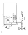
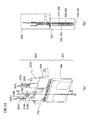
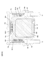
図3,4は本発明に係る実施の形態としての電力変換装置200の外観斜視図であり、図4は交流コネクタ187および直流コネクタ138を外した状態を示す。本実施の形態の電力変換装置200は、平面形状がほぼ正方形の直方体形状としたことにより小型化が図れ、また、車両への取り付けが容易となるという効果を有している。8は蓋、10はハウジング、12は流路形成体、13は冷却媒体の入口配管、14は出口配管、420は下カバーである。コネクタ21は、外部との接続のために設けられた信号用のコネクタである。
3 and 4 are external perspective views of the
蓋8は、電力変換装置200を構成する回路部品が収納されるハウジング10の上部開口部に固定される。ハウジング10の下部に固定される流路形成体12は、後述するパワーモジュール300及びコンデンサモジュール500を保持するとともに、冷却媒体によってこれらを冷却する。冷却媒体としては、例えば水が用いられる場合が多く、以下では冷却水として説明する。入口配管13および出口配管14は流路形成体12の一側面に設けられ、入口配管13から供給された冷却水は流路形成体12内の後述する流路19に流入し、出口配管14から排出される。
The
交流コネクタ187が装着される交流インターフェイス185および直流コネクタ138が装着される直流インターフェイス137は、ハウジング10の側面に設けられている。交流インターフェイス185は配管13,14が設けられている側面に設けられており、交流インターフェイス185に装着された交流コネクタ187の交流配線187aは配管13,14の間を通って下方に延びている。直流インターフェイス137は交流インターフェイス185が設けられた側面に隣接する側面に設けられており、直流インターフェイス137に装着された直流コネクタ138の直流配線138aも電力変換装置200の下方に延びている。
An
このように、交流インターフェイス185と配管13,14とが同一側面12dの側に配置され、交流配線187aが配管13,14の間を通るように下方に引き出されているので、配管13,14、交流コネクタ187および交流配線187aの占める空間を小さくでき、装置全体の大型化を低減できる。また、配管13,14に対して交流配線187aを下方に引き出しているので、交流配線187aの取り回しが容易になり生産性が向上する。
In this way, the
図5は、図4に示す電力変換装置200から蓋8、直流インターフェイス137および交流インターフェイス185を外した状態を示す図である。ハウジング10の一側面には交流インターフェイス185が固定される開口10aが形成され、隣接する他の側面には直流インターフェイス137が固定される開口10bが形成されている。開口10aからは3本の交流バスバー802、すなわち、U相交流バスバー802U、V相交流バスバー802VおよびW相交流バスバー802Wが突出し、開口10bからは直流電源端子508,509が突出している。
FIG. 5 is a diagram showing a state in which
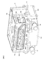
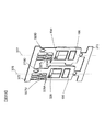
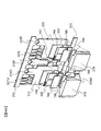
図6は、図5において流路形成体12からハウジング10を外した状態を示す図である。ハウジング10は2つの収納空間を有しており、隔壁10cによって上部収納空間と下部収納空間とに区画されている。上部収納空間にはコネクタ21が固定された制御回路基板20が収納され、下部収納空間にはドライバ回路基板22および後述するバスバーアッセンブリ800が収納される。制御回路基板20には図2に示した制御回路172が実装され、ドライバ回路基板22にはドライバ回路基板174が実装されている。制御回路基板20とドライバ回路基板22とは不図示のフラットケーブル(後述する図7参照)によって接続されるが、そのフラットケーブルは隔壁10cに形成されたスリット状の開口10dを通って下部収納空間から上部収納空間へと引き出される。
6 is a view showing a state where the
図7は電力変換装置200の分解斜視図である。蓋8の内側の、すなわちハウジング10の上部収納空間には、上述したように制御回路172を実装した制御回路基板20が配置されている。蓋8には、コネクタ21用の開口8aが形成されている。電力変換装置200内の制御回路を動作させる低電圧の直流電力は、コネクタ21から供給される。
FIG. 7 is an exploded perspective view of the
詳細は後述するが、流路形成体12には、入口配管13から流入した冷却水が流れる流路が形成されている。流路は、流路形成体12の3つの側面に沿って流れるようなコの字形状の流路を形成している。入口配管13から流入した冷却水はコの字形状流路の一端から流路内に流入し、流路内を流れた後に、流路の他端に接続されている出口配管14から流出される。
Although details will be described later, the flow
流路の上面には3つの開口部400a〜400cが形成されており、直列回路150(図1参照)を内蔵したパワーモジュール300U,300V,300Wがそれらの開口部400a〜400cから流路内に挿入される。パワーモジュール300UにはU相の直列回路150が内蔵され、パワーモジュール300VにはV相の直列回路150が内蔵され、パワーモジュール300WにはW相の直列回路150が内蔵されている。これらパワーモジュール300U〜300Wは同一構成になっており、外観形状も同一形状である。開口部400a〜400cは、挿入されたパワーモジュール300U〜300Wのフランジ部によって塞がれる。
Three openings 400a to 400c are formed on the upper surface of the flow path, and the
流路形成体12には、コの字形状の流路によって囲まれるように、電装部品を収納するための収納空間405が形成されている。本実施形態では、この収納空間405にコンデンサモジュール500が収納されている。収納空間405に収納されたコンデンサモジュール500は、流路内を流れる冷却水によって冷却される。コンデンサモジュール500の上方には、交流バスバー802U〜802Wが装着されたバスバーアッセンブリ800が配置される。バスバーアッセンブリ800は、流路形成体12の上面に固定される。バスバーアッセンブリ800には、電流センサモジュール180が固定されている。
A
ドライバ回路基板22は、バスバーアッセンブリ800に設けられた支持部材807aに固定されることにより、バスバーアッセンブリ800の上方に配置される。上述したように、制御回路基板20とドライバ回路基板22とはフラットケーブル23によって接続される。フラットケーブル23は隔壁10cに形成されたスリット状の開口10dを通って下部収納空間から上部収納空間へと引き出される。
The
このように、パワーモジュール300U〜300Wとドライバ回路基板22と制御回路基板20とが高さ方向に階層的に配置され、制御回路基板20が強電系のパワーモジュール300U〜300Wから最も遠い場所に配置されるので、制御回路基板20側にスイッチングノイズ等が混入するのを低減することができる。さらに、ドライバ回路基板22と制御回路基板20とは隔壁10cによって区画された別の収納空間に配置されるため、隔壁10cが電磁シールドとして機能し、ドライバ回路基板22から制御回路基板20に混入するノイズを低減することができる。なお、ハウジング10はアルミ等の金属材で形成されている。
As described above, the
さらに、ハウジング10に一体に形成された隔壁10cに制御回路基板20が固定されるため、外部からの振動に対して制御回路基板20の機械的な共振周波数が高くなる。そのため、車両側からの振動の影響を受け難く、信頼性が向上する。
Furthermore, since the
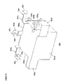
以下では、流路形成体12と、流路形成体12に固定されるパワーモジュール300U〜300W、コンデンサモジュール500およびスバーアッセンブリ800についてより詳しく説明する。図8は、流路形成体12にパワーモジュール300U〜300W、コンデンサモジュール500、バスバーアッセンブリ800を組み付けた外観斜視図である。また、図9は、流路形成体12からバスバーアッセンブリ800を外した状態を示す。バスバーアッセンブリ800は、流路形成体12にボルト固定される。
Hereinafter, the flow
まず、図10,11を参照しながら流路形成体12について説明する。図10は流路形成体12の斜視図であり、図11は流路形成体12を裏面側から見た分解斜視図である。図10に示すように、流路形成体12は平面形状が略正方形の直方体を成し、その側面12dに入口配管13および出口配管14が設けられている。なお、側面12dは、配管13,14が設けられている部分が段差状に形成されている。図11に示すように、流路19は、残りの3つの側面12a〜12cに沿うようにコの字形状に形成されている。そして、流路形成体12の裏面側には、流路19の横断面形状とほぼ同一形状を有する、1つに繋がったコの字形状の開口部404が形成されている。この開口部404は、コの字形状の下カバー420によって塞がれる。下カバー420と流路形成体12との間にはシール部材409aが設けられ、気密性が保たれている。
First, the flow
コの字形状を成す流路19は、冷却水の流れる方向によって3つの流路区間19a,19b,19cに分けられる。詳細は後述するが、第1の流路区間19aは、配管13,14が設けられた側面12dと対向する位置の側面12aに沿って設けられ、第2の流路区間19bは側面12aの一方の側に隣接する側面12bに沿って設けられ、第3の流路区間19cは側面12aの他方の側に隣接する側面12cに沿って設けられている。冷却水は入口配管13から流路区間19bに流入し、破線矢印で示すように流路区間19b、流路区間19a、流路区間19cの順に流れ、出口配管14から流出される。
The
図10に示すように、流路形成体12の上面側には、流路区間19aに対向する位置に側面12aに平行な長方形の開口部402aが形成され、流路区間19bに対向する位置に側面12bに平行な長方形の開口部402bが形成され、流路区間19cに対向する位置に側面12cに平行な長方形の開口部402cが形成されている。これらの開口部402a〜402cを通して、パワーモジュール300U〜300Wが流路19内に挿入される。
As shown in FIG. 10, on the upper surface side of the flow
図11に示すように、下カバー420には、上述した開口部402a〜402cと対向する位置に、流路19の下側に向かって突出する凸部406がそれぞれ形成されている。これらの凸部406は流路19側から見ると窪みとなっており、開口部402a〜402cから挿入されたパワーモジュール300U〜300Wの下端部分が、これらの窪みに入り込む。流路形成体12は、開口部404と開口部402a〜402cとが対向するように形成されているので、アルミ鋳造により製造し易い構成になっている。
As shown in FIG. 11, the
図10に示すように、流路形成体12には、3辺を流路19で囲まれるように形成され矩形状の収納空間405が設けられている。この収納空間405にコンデンサモジュール500が収納される。流路19で囲まれた収納空間405は直方体形状であるため、コンデンサモジュール500を直方体形状にすることができ、コンデンサモジュール500の生産性が良くなる。
As shown in FIG. 10, the flow
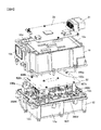
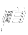
図12乃至図26を用いてインバータ回路140に使用されるパワーモジュール300U〜300Wおよびパワーモジュール301U〜301Wの詳細構成を説明する。上記パワーモジュール300U〜300Wおよびパワーモジュール301U〜301Wはいずれも同じ構造であり、代表してパワーモジュール300Uの構造を説明する。尚、図12乃至図26において信号端子325Uは、図2に開示したゲート電極154および信号用エミッタ電極155に対応し、信号端子325Lは、図2に開示したゲート電極164およびエミッタ電極165に対応する。また直流正極端子315Bは、図2に開示した正極端子157と同一のものであり、直流負極端子319Bは、図2に開示した負極端子158と同一のものである。また交流端子320Bは、図2に開示した交流端子159と同じものである。
Detailed configurations of the
図12(a)は、本実施形態のパワーモジュール300Uの斜視図である。図12(b)は、本実施形態のパワーモジュール300Uを断面Dで切断して方向Eから見たときの断面図である。
FIG. 12A is a perspective view of the
図13は、理解を助けるために、図12に示す状態からネジ309および第二封止樹脂351を取り除いたパワーモジュール300Uを示す図である。図13(a)は斜視図であり、図13(b)は図12(b)と同様に断面Dで切断して方向Eから見たときの断面図である。また、図13(c)はフィン305が加圧されて湾曲部304Aが変形される前の断面図を示している。
FIG. 13 is a diagram showing a
図14は、図13に示す状態からさらにモジュールケース304を取り除いたパワーモジュール300Uを示す図である。図14(a)は斜視図であり、図14(b)は図12(b)、図13(b)と同様に断面Dで切断して方向Eから見たときの断面図である。
FIG. 14 is a diagram showing a
図15は、図14に示す状態からさらに第一封止樹脂348および配線絶縁部608を取り除いたパワーモジュール300Uの斜視図である。
FIG. 15 is a perspective view of the
図16は、パワーモジュール300Uのうちの補助モールド体600を示す図である。図16(a)は斜視図であり、図16(b)は図12(b)、図13(b)および図14(b)と同様に断面Dで切断して方向Eから見たときの断面図である。
FIG. 16 is a diagram showing an
上下アームの直列回路150を構成するパワー半導体素子(IGBT328、IGBT330、ダイオード156、ダイオード166)が、図14および15に示す如く、導体板315や導体板318によって、あるいは導体板320や導体板319によって、両面から挟んで固着される。導体板315等は、その放熱面が露出した状態で第一封止樹脂348によって封止され、当該放熱面に絶縁シート333が熱圧着される。第一封止樹脂348は図14に示すように、多面体形状(ここでは略直方体形状)を有している。
As shown in FIGS. 14 and 15, the power semiconductor elements (
第一封止樹脂348により封止されたモジュール一次封止体302は、モジュールケース304の中に挿入して絶縁シート333を挟んで、CAN型冷却器であるモジュールケース304の内面に熱圧着される。ここで、CAN型冷却器とは、一面に挿入口306と他面に底を有する筒形状をした冷却器である。モジュールケース304の内部に残存する空隙には、第二封止樹脂351を充填される。
The module
モジュールケース304は、電気伝導性を有する部材、例えばアルミ合金材料(Al,AlSi,AlSiC,Al−C等)で構成され、かつ、つなぎ目の無い状態で一体に成形される。モジュールケース304は、挿入口306以外に開口を設けない構造であり、挿入口306は、フランジ304Bよって、その外周を囲まれている。また、図12(a)に示されるように、他の面より広い面を有する第1放熱面307A及び第2放熱面307Bがそれぞれ対向した状態で配置され、これらの放熱面に対向するようにして、各パワー半導体素子(IGBT328、IGBT330、ダイオード156、ダイオード166)が配置されている。当該対向する第1放熱面307Aと第2放熱面307Bと繋ぐ3つの面は、当該第1放熱面307A及び第2放熱面307Bより狭い幅で密閉された面を構成し、残りの一辺の面に挿入口306が形成される。モジュールケース304の形状は、正確な直方体である必要が無く、角が図12(a)に示す如く曲面を成していても良い。
The
このような形状の金属製のケースを用いることで、モジュールケース304を水や油などの冷媒が流れる流路19内に挿入しても、冷媒に対するシールをフランジ304Bにて確保できるため、冷却媒体がモジュールケース304の内部に侵入するのを簡易な構成で防ぐことができる。また、対向した第1放熱面307Aと第2放熱面307Bに、フィン305がそれぞれ均一に形成される。さらに、第1放熱面307A及び第2放熱面307Bの外周には、厚みが極端に薄くなっている湾曲部304Aが形成されている。湾曲部304Aは、フィン305を加圧することで簡単に変形する程度まで厚みを極端に薄くしてあるため、モジュール一次封止体302が挿入された後の生産性が向上する。
By using the metal case having such a shape, even when the
上述のように導体板315等を絶縁シート333を介してモジュールケース304の内壁に熱圧着することにより、導体板315等とモジュールケース304の内壁の間の空隙を少なくすることができ、パワー半導体素子の発生熱を効率良くフィン305へ伝達できる。さらに絶縁シート333にある程度の厚みと柔軟性を持たせることにより、熱応力の発生を絶縁シート333で吸収することができ、温度変化の激しい車両用の電力変換装置に使用するのに良好となる。
As described above, the gap between the
モジュールケース304の外には、コンデンサモジュール500と電気的に接続するための金属製の直流正極配線315Aおよび直流負極配線319Aが設けられており、その先端部に直流正極端子315B(157)と直流負極端子319B(158)がそれぞれ形成されている。また、モータジェネレータMG1あるいはMG2に交流電力を供給するための金属製の交流配線320Aが設けられており、その先端に交流端子320B(159)が形成されている。本実施形態では、図15に示す如く、直流正極配線315Aは導体板315と接続され、直流負極配線319Aは導体板319と接続され、交流配線320Aは導体板320と接続される。
Outside the
モジュールケース304の外にはさらに、ドライバ回路174と電気的に接続するための金属製の信号配線324Uおよび324Lが設けられており、その先端部に信号端子325U(154,155)と信号端子325L(164,165)がそれぞれ形成されている。本実施形態では、図15に示す如く、信号配線324UはIGBT328と接続され、信号配線324LはIGBT328と接続される。
In addition to the
直流正極配線315A、直流負極配線319A、交流配線320A、信号配線324Uおよび信号配線324Lは、樹脂材料で成形された配線絶縁部608によって相互に絶縁された状態で、補助モールド体600として一体に成型される。配線絶縁部608は、各配線を支持するための支持部材としても作用し、これに用いる樹脂材料は、絶縁性を有する熱硬化性樹脂かあるいは熱可塑性樹脂が適している。これにより、直流正極配線315A、直流負極配線319A、交流配線320A、信号配線324Uおよび信号配線324Lの間の絶縁性を確保でき、高密度配線が可能となる。補助モールド体600は、モジュール一次封止体302と接続部370において金属接合された後に、配線絶縁部608に設けられたネジ穴を貫通するネジ309によってモジュールケース304に固定される。接続部370におけるモジュール一次封止体302と補助モールド体600との金属接合には、たとえばTIG溶接などを用いることができる。
The DC
直流正極配線315Aと直流負極配線319Aは、配線絶縁部608を間に挟んで対向した状態で互いに積層され、略平行に延びる形状を成している。こうした配置および形状とすることで、パワー半導体素子のスイッチング動作時に瞬間的に流れる電流が、対向してかつ逆方向に流れる。これにより、電流が作る磁界が互いに相殺する作用をなし、この作用により低インダクタンス化が可能となる。なお、交流配線320Aや信号端子325U,325Lも、直流正極配線315A及び直流負極配線319Aと同様の方向に向かって延びている。
The direct current
モジュール一次封止体302と補助モールド体600が金属接合により接続されている接続部370は、第二封止樹脂351によりモジュールケース304内で封止される。これにより、接続部370とモジュールケース304との間で必要な絶縁距離を安定的に確保することができるため、封止しない場合と比較してパワーモジュール300Uの小型化が実現できる。
The
図15、図16に示されるように、接続部370の補助モジュール600側には、補助モジュール側直流正極接続端子315C、補助モジュール側直流負極接続端子319C、補助モジュール側交流接続端子320C、補助モジュール側信号接続端子326Uおよび補助モジュール側信号接続端子326Lが一列に並べて配置される。一方、接続部370のモジュール一次封止体302側には、多面体形状を有する第一封止樹脂348の一つの面に沿って、素子側直流正極接続端子315D、素子側直流負極接続端子319D、素子側交流接続端子320D、素子側信号接続端子327Uおよび素子側信号接続端子327Lが一列に並べて配置される。こうして接続部370において各端子が一列に並ぶような構造とすることで、トランスファーモールドによるモジュール一次封止体302の製造が容易となる。
As shown in FIGS. 15 and 16, the
ここで、モジュール一次封止体302の第一封止樹脂348から外側に延出している部分をその種類ごとに一つの端子として見た時の各端子の位置関係について述べる。以下の説明では、直流正極配線315A(直流正極端子315Bと補助モジュール側直流正極接続端子315Cを含む)および素子側直流正極接続端子315Dにより構成される端子を正極側端子と称し、直流負極配線319A(直流負極端子319Bと補助モジュール側直流負極接続端子319Cを含む)および素子側直流負極接続端子315Dにより構成される端子を負極側端子と称し、交流配線320A(交流端子320Bと補助モジュール側交流接続端子320Cを含む)および素子側交流接続端子320Dにより構成される端子を出力端子と称し、信号配線324U(信号端子325Uと補助モジュール側信号接続端子326Uを含む)および素子側信号接続端子327Uにより構成される端子を上アーム用信号端子と称し、信号配線324L(信号端子325Lと補助モジュール側信号接続端子326Lを含む)および素子側信号接続端子327Lにより構成される端子を下アーム用信号端子と称する。
Here, the positional relationship of each terminal when the portion extending outward from the
上記の各端子は、いずれも第一封止樹脂348および第二封止樹脂351から接続部370を通して突出しており、その第一封止樹脂348からの各突出部分(素子側直流正極接続端子315D、素子側直流負極接続端子319D、素子側交流接続端子320D、素子側信号接続端子327Uおよび素子側信号接続端子327L)は、上記のように多面体形状を有する第一封止樹脂348の一つの面に沿って一列に並べられている。また、正極側端子と負極側端子は、第二封止樹脂351から積層状態で突出しており、モジュールケース304の外に延出している。このような構成としたことで、第一封止樹脂348でパワー半導体素子を封止してモジュール一次封止体302を製造する時の型締めの際に、パワー半導体素子と当該端子との接続部分への過大な応力や金型の隙間が生じるのを防ぐことができる。また、積層された正極側端子と負極側端子の各々を流れる反対方向の電流により、互いに打ち消しあう方向の磁束が発生されるため、低インダクタンス化を図ることができる。
Each of the above terminals protrudes from the
補助モジュール600側において、補助モジュール側直流正極接続端子315C、補助モジュール側直流負極接続端子319Cは、直流正極端子315B、直流負極端子319Bとは反対側の直流正極配線315A、直流負極配線319Aの先端部にそれぞれ形成されている。また、補助モジュール側交流接続端子320Cは、交流配線320Aにおいて交流端子320Bとは反対側の先端部に形成されている。補助モジュール側信号接続端子326U、326Lは、信号配線324U、324Lにおいて信号端子325U、325Lとは反対側の先端部にそれぞれ形成されている。
On the
一方、モジュール一次封止体302側において、素子側直流正極接続端子315D、素子側直流負極接続端子319D、素子側交流接続端子320Dは、導体板315、319、320にそれぞれ形成されている。また、素子側信号接続端子327U、327Lは、ボンディングワイヤ371によりIGBT328、330とそれぞれ接続されている。
On the other hand, on the module
次に、図17乃至図21を用いてモジュール一次封止体302の組立工程を説明する。
Next, the assembly process of the module
図17に示すように、直流正極側の導体板315および交流出力側の導体板320と、素子側信号接続端子327Uおよび327Lとは、共通のタイバー372に繋がれた状態で、これらが略同一平面状の配置となるように一体的に加工される。導体板315には、上アーム側のIGBT328のコレクタ電極と上アーム側のダイオード156のカソード電極が固着される。導体板320には、下アーム側のIGBT330のコレクタ電極と下アーム側のダイオード166のカソード電極が固着される。IGBT328,330およびダイオード155,166の上には、導体板318と導体板319が略同一平面状に配置される。導体板318には、上アーム側のIGBT328のエミッタ電極と上アーム側のダイオード156のアノード電極が固着される。導体板319には、下アーム側のIGBT330のエミッタ電極と下アーム側のダイオード166のアノード電極が固着される。各パワー半導体素子は、各導体板に設けられた素子固着部322に、金属接合材160を介してそれぞれ固着される。金属接合材160は、例えばはんだ材や銀シート及び微細金属粒子を含んだ低温焼結接合材、等である。
As shown in FIG. 17, the DC positive electrode
各パワー半導体素子は板状の扁平構造であり、当該パワー半導体素子の各電極は表裏面に形成されている。図17に示されるように、パワー半導体素子の各電極は、導体板315と導体板318、または導体板320と導体板319によって挟まれる。つまり、導体板315と導体板318は、IGBT328及びダイオード156を介して略平行に対向した積層配置となる。同様に、導体板320と導体板319は、IGBT330及びダイオード166を介して略平行に対向した積層配置となる。また、導体板320と導体板318は中間電極329を介して接続されている。この接続により上アーム回路と下アーム回路が電気的に接続され、上下アーム直列回路が形成される。
Each power semiconductor element has a flat plate-like structure, and each electrode of the power semiconductor element is formed on the front and back surfaces. As shown in FIG. 17, each electrode of the power semiconductor element is sandwiched between a
上述したように、導体板315と導体板318の間にIGBT328及びダイオード156を挟み込むと共に、導体板320と導体板319の間にIGBT330及びダイオード166を挟み込み、導体板320と導体板318を中間電極329を介して接続することで、図18のようになる。その後、IGBT328の制御電極328Aと素子側信号接続端子327Uとをボンディングワイヤ371により接続すると共に、IGBT330の制御電極330Aと素子側信号接続端子327Lとをボンディングワイヤ371により接続することで、図19のようになる。
As described above, the
図19に示す状態まで組み立てられたら、パワー半導体素子およびボンディングワイヤ371を含む部分を第一封止樹脂348により図20のように封止する。このとき、金型押圧面373において上下から金型で押さえ、トランスファーモールドにより第一封止樹脂348を金型内に充填して成形する。
When assembled to the state shown in FIG. 19, the portion including the power semiconductor element and the
第一封止樹脂348により封止したら、タイバー372を切除して、素子側直流正極接続端子315D、素子側交流接続端子320D、素子側信号接続端子327U、327Lをそれぞれ分離する。そして、モジュール一次封止体302の一辺側に一列に並べられている素子側直流正極接続端子315D、素子側直流負極接続端子319D、素子側交流接続端子320D、素子側信号接続端子327U、327Lの各端部を、図21のようにそれぞれ同一方向に折り曲げる。これにより、接続部370においてモジュール一次封止体302と補助モールド体600とを金属接合する際の作業を容易化して生産性を向上すると共に、金属接合の信頼性を向上することができる。
After sealing with the
図22は、第一封止樹脂348のトランスファーモールド工程を説明するための図である。図22(a)は型締め前の縦断面図を示しており、(b)は型締め後の縦断面図を示している。
FIG. 22 is a view for explaining the transfer molding process of the
図22(a)に示すように、図19に示した封止前のモジュール一次封止体302は、上側金型374Aと下側金型374Bの間に設置される。上側金型374Aおよび下側金型374Bがモジュール一次封止体302を上下から金型押圧面373において挟み込んで型締めすることで、図22(b)に示すように金型空間375が金型内に形成される。この金型空間375に第一封止樹脂348を充填して成形することで、モジュール一次封止体302においてパワー半導体素子(IGBT328,330およびダイオード155,166)が第一封止樹脂348により封止される。
As shown in FIG. 22A, the module
なお、図20に示したように、金型押圧面373では、素子側直流正極接続端子315D、素子側直流負極接続端子319D、素子側交流接続端子320D、素子側信号接続端子327Uおよび素子側信号接続端子327Lが一列に並べて配置されている。こうした端子配置とすることで、上側金型374Aおよび下側金型374Bを用いて、各端子とパワー半導体素子との接続部において余分な応力を発生させずに、かつ隙間なく型締めを行うことができる。したがって、パワー半導体素子の破損を招いたり、あるいは第一封止樹脂348が隙間から漏出したりすることなく、パワー半導体素子の封止を行うことができる。
As shown in FIG. 20, on the
次に、モジュール一次封止体302におけるパワー半導体素子の制御電極と各端子との配置関係について、図23を参照して説明する。図23では、理解を容易にするため、図18の状態から導体板318,319および中間電極329を除いた様子を示している。図23において、IGBT328,330の一辺側(図中の上辺側)には、制御電極328A,330Aが中心線376,377に対して図中左側に偏った位置にそれぞれ配置されている。中心線376,377は、素子側直流正極接続端子315D、素子側直流負極接続端子319D、素子側交流接続端子320D、素子側信号接続端子327Uおよび素子側信号接続端子327Lの配列方向に直交している。
Next, the arrangement relationship between the control electrode and each terminal of the power semiconductor element in the module
IGBT328を中心線376で二分して考えると、制御電極328Aが配置されている一方側には素子側信号接続端子327Uが配置されており、他方側には素子側直流正極接続端子315Dが配置されている。同様に、IGBT330を中心線377で二分して考えると、制御電極330Aが配置されている一方側には素子側信号接続端子327Lが配置されており、他方側には素子側交流接続端子320Dが配置されている。また図18に示すように、素子側直流正極接続端子315Dと素子側信号接続端子327Lの間には、素子側直流負極接続端子319Dが配置される。こうした配置とすることで、制御電極328A,330Aと素子側信号接続端子327U,327Lとをそれぞれ接続するボンディングワイヤ371の長さを最小化し、接続の信頼性を向上することができる。また、各端子を集約化してモジュール一次封止体302、ひいてはパワーモジュール300Uの小型化を図ることができる。
When the
なお、図23に示すように、素子側直流正極接続端子315D、素子側交流接続端子320D、素子側信号接続端子327Uおよび素子側信号接続端子327Lは、共通のタイバー372に繋がれた状態で一体的に加工される。これにより、これら各端子の間では平面度や厚さのばらつきを非常に小さく抑えることができる。その一方で、素子側直流負極接続端子319Dは、上記の各端子とは別体に加工されたものが組み合わされるため、平面度や厚さのばらつきが他の各端子と比べて大きくなり、型締め時に当該端子とパワー半導体素子との接続部において余分な応力を生じてしまう可能性がある。
As shown in FIG. 23, the element-side DC positive
図24は、上述したような不都合を回避するための変形例を示す図である。この変形例では、素子側直流負極接続端子319Dが設けられている導体板319において、型締め時の応力を吸収して緩和するための応力緩和部319Eが設けられている。応力緩和部319Eの位置は、パワー半導体素子が実装される部分(はんだ付け部分)から金型押圧面373の間とすることが好ましい。なお、応力緩和部319Eとして単に導体板319の一部の厚みを他の部分より薄くすることも考えられるが、その場合は当該部分において電流密度が増加することになるため、電気的性能が低下するおそれがある。したがって、図24に示すように導体板319の一部を屈曲させて応力緩和部319Eとすることが好ましい。このようにすれば、応力緩和部319Eにおいて電流密度が増加することもなく、さらに屈曲による折り返し部分において電流の向きが対向することになるため、インダクタンスの抑制にも寄与することができる。
FIG. 24 is a diagram illustrating a modification for avoiding the above-described inconvenience. In this modification, the
図25は、パワーモジュール300Uの回路構成を示す回路図である。上アーム側のIGBT328のコレクタ電極と上アーム側のダイオード156のカソード電極は、導体板315を介して接続される。同様に、下アーム側のIGBT330のコレクタ電極と下アーム側のダイオード166のカソード電極は、導体板320を介して接続される。また、上アーム側のIGBT328のエミッタ電極と上アーム側のダイオード156のアノード電極は、導体板318を介して接続される。同様に、下アーム側のIGBT330のエミッタ電極と下アーム側のダイオード166のアノード電極は、導体板319を介して接続される。導体板318と320は中間電極329によって接続される。こうした回路構成により上下アーム直列回路が形成される。
FIG. 25 is a circuit diagram showing a circuit configuration of the
次に、低インダクタンス化が生じる作用について、図26を参照して説明する。図26(a)はリカバリ電流が流れる際の等価回路を示す図であり、図26(b)はリカバリ電流の経路を示す図である。 Next, the action of reducing the inductance will be described with reference to FIG. FIG. 26A is a diagram showing an equivalent circuit when a recovery current flows, and FIG. 26B is a diagram showing a path of the recovery current.
図26(a)において、下アーム側のダイオード166が順方向バイアス状態で導通している状態とする。この状態で、上アーム側のIGBT328がON状態になると、下アーム側のダイオード166が逆方向バイアスとなりキャリア移動に起因するリカバリ電流が上下アームを貫通する。このとき、各導体板315,318,319,320には、図26(b)に示されるリカバリ電流360が流れる。リカバリ電流360は、点線で示されるとおり、直流負極端子319B(158)と対向に配置された直流正極端子315B(157)を通り、続いて各導体板315,318,319,320により形成されるループ形状の経路を流れ、再び直流正極端子315B(157)と対向に配置された直流負極端子319B(158)を介して実線に示すように流れる。ループ形状経路を電流が流れることによって、モジュールケース304の第1放熱面307A及び第2放熱面307Bに渦電流361が流れる。この渦電流361の電流経路に等価回路362が発生する磁界相殺効果によって、ループ形状経路における配線インダクタンス363が低減する。
In FIG. 26A, it is assumed that the
なお、リカバリ電流360の電流経路がループ形状に近いほど、インダクタンス低減作用が増大する。本実施形態では、ループ形状の電流経路は点線で示す如く、導体板315の直流正極端子315B(157)側に近い経路を流れ、IGBT328及びダイオード156内を通る。そしてループ形状の電流経路は実線で示す如く、導体板318の直流正極端子315B(157)側より遠い経路を流れ、その後、点線で示す如く導体板320の直流正極端子315B(157)側より遠い経路を流れ、IGBT330及びダイオード166内を通る。さらにループ形状の電流経路は実線で示す如く、導体板319の直流負極配線319A側に近い経路を流れる。このようにループ形状の電流経路が、直流正極端子315B(157)や直流負極端子319B(158)に対して、近い側や遠い側の経路を通ることで、よりループ形状に近い電流経路が形成される。
Note that the closer the current path of the recovery current 360 is to the loop shape, the greater the inductance reduction action. In the present embodiment, the loop-shaped current path flows through a path close to the DC
図38は、直流負極配線を分割した場合の変形例を示す図である。なお、前述した符号と同一符号の構成は、同一の機能を有する。図18にて示された素子側直流負極接続端子319Dは、上記の各端子とは別体に加工されたものが組み合わされるため、平面度や厚さのばらつきが他の各端子と比べて大きくなり、型締め時に当該端子とパワー半導体素子との接続部において余分な応力を生じてしまう可能性がある。
FIG. 38 is a diagram illustrating a modification in the case where the DC negative electrode wiring is divided. In addition, the structure of the same code | symbol as the code | symbol mentioned above has the same function. The element-side DC negative
そこで、図38に示されるように、図18にて示された素子側直流負極接続端子319Dを分割して、の負極側接続端子319Fが素子側交流接続端子320Dや素子側直流正極接続端子315Dと略同一面上に配置される。
Therefore, as shown in FIG. 38, the element-side DC
また、図39に示されるように、素子側直流負極接続端子319Gが導体319の縁辺から負極側接続端子319Fの一部と対向する位置まで延ばされている。そして、素子側直流負極接続端子319Gの端部は、負極側接続端子319F側に折り曲げられる。
As shown in FIG. 39, the element-side DC negative
そして、図40に示されるように、素子側直流負極接続端子319Gの端部が、金属接合材161を介して負極側接続端子319Fと接続される。各種の半導体素子及び端子を金属接合材により接合した後に、図22に示される製造方法により、図40に示されたモジュール体を第1封止樹脂348によって封止すると、図41に示されるモジュール1次封止体303が完成する。図41に示されるように、負極側接続端子319Fは、素子側直流正極接続端子315Dや素子側交流接続端子320Dや素子側信号接続端子327Uとともに、タイバー372と一体に形成される。そして、タイバー372の切断は、負極側接続端子319Fとの接続部分を含めて一括して行うことが出来る。
As shown in FIG. 40, the end of the element-side DC negative
これにより、これら各端子の間では平面度や厚さのばらつきを非常に小さく抑えることができる。 As a result, variations in flatness and thickness between these terminals can be minimized.
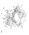
図27は、コンデンサモジュール500の外観斜視図である。コンデンサモジュール500内には複数のコンデンサセルが設けられている。コンデンサモジュール500の上面には、コンデンサモジュール500の流路19に対向する面に近接して、コンデンサ端子503a〜503cが突出するように設けられている。コンデンサ端子503a〜503cは、各パワーモジュール300の正極端子157及び負極端子158に対応して形成される。コンデンサ端子503a〜503cは同一形状を成し、コンデンサ端子503a〜503cを構成する負極側コンデンサ端子504と正極側コンデンサ端子506との間には絶縁シートが設けられ、端子間の絶縁が確保されている。
FIG. 27 is an external perspective view of the
コンデンサモジュール500の側面500dの側の上部には、突出部500e,500fが形成されている。突出部500e内には放電抵抗が実装され、突出部500f内にはコモンモードノイズ対策用のYコンデンサが実装されている。また、突出部500fの上面から突出した端子500g,500hに、図5に示した電源端子508,509が取り付けられる。図10に示すように、開口402b,402cと側面12dとの間には凹部405a,405bが形成されており、コンデンサモジュール500を流路形成体12の収納空間405に収納すると、突出部500eは凹部405aに収納され、突出部500fは凹部405bに収納される。
突出部500e内に実装された放電抵抗は、インバータ停止時にコンデンサモジュール500内のコンデンサセルに溜まった電荷を放電するための抵抗である。突出部500eが収納される凹部405aは、入口配管13から流入した冷却水の流路の直上に設けられているので、放電時の放電抵抗の温度上昇を抑えることができる。
The discharge resistor mounted in the
図28は、バスバーアッセンブリ800の斜視図である。バスバーアッセンブリ800は、U,V,W相の交流バスバー802U,802V,802Wと、交流バスバー802U〜802Wを保持し固定するための保持部材803と、交流バスバー802U〜802Wを流れる交流電流を検出するための電流センサモジュール180と、を備えている。交流バスバー802U〜802Wは、それぞれ幅広導体で形成されている。樹脂等の絶縁材料で形成された保持部材803には、ドライバ回路基板22を保持するための複数の支持部材807aが、保持部材803から上方に突出するように形成されている。
FIG. 28 is a perspective view of the
電流センサモジュール180は、前述した図8に示すようにバスバーアッセンブリ800を流路形成体12上に固体したときに、流路形成体12の側面12dに近接した位置で側面12dに平行となるように、バスバーアッセンブリ800に配置されている。図28に示すように、電流センサモジュール180の側面には、交流バスバー802U〜802Wを貫通させるための貫通孔181がそれぞれ形成されている。電流センサモジュール180の貫通孔181が形成されている部分にはセンサ素子が設けられており、電流センサモジュール180の上面から各センサ素子の信号線182aが突出している。各センサ素子は、電流センサモジュール180の延在方向、すなわち流路形成体12の側面12dの延在方向に並んで配置されている。交流バスバー802U〜802Wは各貫通孔181を貫通し、その先端部分が平行に突出している。
The
保持部材803には、位置決め用の突起部806a,806bが上方に向かって突出するように形成されている。電流センサモジュール180はネジ止めにより保持部材803に固定されるが、その際に突起部806a,806bと電流センサモジュール180の枠体に形成された位置決め孔とを係合させることで、電流センサモジュール180の位置決めが行われる。さらに、ドライバ回路基板22を支持部材807aに固定する際に、ドライバ回路基板22側に形成された位置決め孔に位置決め用突起部806a,806bを係合させることで、電流センサモジュール180の信号線182aがドライバ回路基板22のスルーホールに位置決めされる。信号線182aは、ドライバ回路基板22の配線パターンと半田によって接合される。
On the holding
本実施形態では、保持部材803、支持部材807a及び突起部806a,806bは、樹脂で一体に形成される。 このように、保持部材803が電流センサモジュール180とドライバ回路基板22との位置決め機能を備えることになるので、信号線182aとドライバ回路基板22との間の組み付け及び半田接続作業が容易になる。また、電流センサモジュール180とドライバ回路基板22を保持する機構を保持部材803に設けることで、電力変換装置全体としての部品点数を削減できる。
In the present embodiment, the holding
交流バスバー802U〜802Wは幅広面が水平となるように保持部材803に固定され、パワーモジュール300U〜300Wの交流端子159に接続される接続部805が垂直に立ち上がっている。接続部805は先端が凹凸形状をしており、溶接時にこの凹凸部分に熱が集中するような形状となっている。
The
上述したように電流センサモジュール180は流路形成体12の側面12dに平行に配置されているので、電流センサモジュール180の貫通孔181から突出した各交流バスバー802U〜802Wは、流路形成体12の側面12dに配置されることになる。各パワーモジュール300U〜300Wは、流路形成体12の側面12a,12b,12cに沿って形成された流路区間19a,19b,19cに配置されるので、交流バスバー802U〜802Wの接続部805は、バスバーアッセンブリ800の側面12a〜12bに対応する位置に配置される。その結果、図8に示すように、U相交流バスバー802Uは側面12bの近傍に配置されたパワーモジュール300Uから側面12dまで延接され、V相交流バスバー802Vは側面12aの近傍に配置されたパワーモジュール300Vから側面12dまで延接され、W相交流バスバー802Wは側面12cの近傍に配置されたパワーモジュール300Wから側面12dまで延設される。
Since the
図29は、開口部402a〜402cにパワーモジュール300U〜300Wが固定され、収納空間405にコンデンサモジュール500が収納された流路形成体12を示す図である。図29に示す例では、開口部402bにU相のパワーモジュール300Uが固定され、開口部402aにV相のパワーモジュール300Vが固定され、開口部402cにW相のパワーモジュール300Wが固定される。その後、コンデンサモジュール500が収納空間405に収納され、コンデンサ側の端子と各パワーモジュールの端子とが溶接等により接続される。各端子は、流路形成体12の上端面から突出しており、上方から溶接機をアプローチして溶接作業が行われる。
FIG. 29 is a diagram illustrating the flow
なお、コの字形状に配置された各パワーモジュール300U〜300Wの正極及び負極端子157,158は、コンデンサモジュール500の上面に突出して設けられたコンデンサ端子503a〜503cと接続される。3つのパワーモジュール300U〜300Wはコンデンサモジュール500を囲むように設けられているため、コンデンサモジュール500に対する各パワーモジュール300U〜300Wの位置的関係が同等となり、同一形状のコンデンサ端子503a〜503cを用いてバランス良くコンデンサモジュール500に接続することができる。そのため、コンデンサモジュール500とパワーモジュール300U〜300Wとの回路定数が3相の各相においてバランスし易くなり、電流の出し入れがし易い構造となっている。
The positive and
図30は、図29に示すようにパワーモジュール300U〜300Wおよびコンデンサモジュール500が配置された流路形成体12を、水平に断面した図である。上述したように、流路形成体12にはコの字形状の流路19が形成されており、図示左側の側面12bに沿って形成された流路区間19bには、U相パワーモジュール300Uが配置されている。同様に、配管13,14が設けられた側面12dと反対側の側面12aに沿って形成された流路区間19aには、V相パワーモジュール300Vが配置され、右側の側面12に沿って形成された流路区間19cにはW相パワーモジュール300Wが配置されている。
FIG. 30 is a horizontal cross-sectional view of the flow
流路形成体12の側面12dには、開口12g、12hが形成されている。開口12gは連通路12eを介して流路区間19bと連通している。開口12hは連通路12fを介して流路区間19cと連通している。開口12g、12hに配置される配管13,14は、連通路12e,12fに圧入されるように取り付けられている。
図37は、図30のAA断面の矢印方向から見た流路形成体12の断面図を示す。連通路12fは、冷却水の流れ方向に沿った流路断面の形状は大きく変化している。また、本実施形態の冷却水は、パワーモジュール300Uの側面によって、その流れが2つに分岐され、一方の流れはモジュールケース304の第1放熱面307A側に向かい、かつ他方の流れはモジュールケース304の第2放熱面307B側に向かう。なお、第1放熱面307Aは図37に示す第2放熱面307Bと逆側の放熱面であり、図37では見えていない。よって、本実施形態の冷却水がパワーモジュール300Uの側面と衝突することにより、当該冷却水を流す為の圧力損失が大きくなる傾向がある。この圧力損失の増大を抑制するために、パワーモジュール300Uの側面部の近傍において、冷却水の流れを整える必要がある。そこで、助走区間12jは、入口配管13側からパワーモジュール300Uに向かう方向に、段階的に高さ方向の幅が大きくなるように形成されている。なお、助走区間12jの形状は、図37のように階段状に形成されるのではなく、滑らかなスロープ状であってもよい。
FIG. 37 shows a cross-sectional view of the flow
本実施の形態では、平面形状が略正方形の流路形成体12の3つの側面12a〜12cに沿ってコの字形状の流路19を形成し、パワーモジュール300U〜300Wを各流路区間19a〜19cに配置する際に、扁平なパワーモジュール300U〜300Wを各側面12a〜12cに平行に配置するようにした。そして、流路19によって囲まれた中央領域(収納空間405)に、電装部品であるコンデンサモジュール500を収納するようにした。このようなモジュール配置とすることにより、パワーモジュール300U〜300Wおよびコンデンサモジュール500が収納される流路形成体12の小型化が図れる。
In the present embodiment, the
なお、3つのパワーモジュール300U〜300Wをコの字形状に配置する場合、図30に示すように、平行に配置された一対のパワーモジュール300U,300Wの間に配置されるパワーモジュール300Vの少なくとも一部が、パワーモジュール300Uと300Wとで挟まれた領域に入り込むように配置することで、より小型化を図ることができる。
When the three
図31は、3つのパワーモジュール300U〜300Wの配置を説明するための模式図である。なお、パワーモジュール300U〜300Wは同一構造、同一形状を有している。流路形成体の側面12b、12cの幅は、少なくともパワーモジュール300U〜300Wの流路に沿った長さL1と連通路の長さL2との合計程度が必要である。一方、側面12aに関しては、少なくとも寸法L1程度が必要になる。もちろん、実際上は、図30に示すように、流路区間の接続部分など冷却水の流れを考慮して寸法を若干調整する必要がある。
FIG. 31 is a schematic diagram for explaining the arrangement of the three
そのため、電力変換装置20の設置面積をなるべく小さくしようとした場合、平面視で見たときの形状(平面形状)を略正方形とすることで、電力変換装置200の小型化を図ることが考えられる。上述のように側面12b,12cに沿った方向に関しては連通路が必要であるため、小型化の観点から、図31に示すように、一対のパワーモジュール300U,300Wの間の領域S1にパワーモジュール300Vの一部が含まれるように、パワーモジュール300Vを配置するのが好ましい。
Therefore, when trying to reduce the installation area of the
図31における配置スペースの図示横方向の寸法(側面12aの幅寸法)は、パワーモジュールの厚さをL3とすると、少なくともL1+2・L3程度となる。そこで、縦方向の寸法L1+L2+(L3−L4)がL1+L3と同程度となるように、L3およびL4を設定すれば、平面視における面積をより小さくすることができ、略正方形とすることも可能となる。このとき流路区間19aは、図30に示すようにパワーモジュール300U,300Wの間の領域を通るように形成される。なお、図30に示す例では、コンデンサモジュール500の寸法による制約のために、パワーモジュール300U,300Wの間隔は、パワーモジュール300Vの寸法L1よりも若干大きくなっている。
The horizontal dimension (width dimension of the
配管13,14およびそれらが圧入される孔12e,孔12fの上部領域は空きスペースとなる。そこで、図10に示すように、このスペースに凹部405a,405bを形成し、図29のようにコンデンサモジュール500の放電抵抗実装部である突出部500eと、Yコンデンサ実装部である突出部500fとを配置することで、空きスペースの有効利用が図れ、電力変換装置200の小型化に寄与する。配管13,14の位置を一つの側面12dに集約することで、入口配管13から流路区間19bまで、および流路区間19cから出口配管14までの冷却水の流れが直線状になるので、圧損を極力小さくすることができる。また、配管の突出による装置の設置スペースが大きくなるのを抑えることができると共に、車載性の向上を図ることができる。さらに、配管13,14を孔12e,12fに圧入する際に、筐体の一面のみでの圧入作業であるため、作業性および生産性が向上する。
The upper areas of the
また、コンデンサモジュール500の3辺を囲むように流路19が設けられているため、コンデンサモジュール500を効果的に冷却することができる。ところで、本実施の形態における電力変換装置200は車載用であって、一般的にエンジンルーム内に配置される場合が多い。エンジンルーム内はエンジンや走行用モータなどからの熱により比較的高温となるため、電力変換装置200に対する周囲からの熱侵入が問題となる。しかし、図30に示すように、コンデンサモジュール500は冷却水が流れる流路19によって3辺を囲まれているので、装置周囲からの熱侵入を効果的に遮断することができる。
Further, since the
図29に示すように流路形成体12にパワーモジュール300U〜300Wおよびコンデンサモジュール500を配置したならば、図8に示すようにコンデンサモジュール500の上方にバスバーアッセンブリ800を固定し、端子の溶接作業を行う。本実施の形態では、コの字形状に配置されたパワーモジュール300U〜300Wの端子に接続されるバスバー802U〜802Wを、各接続部から離れるようにコンデンサモジュール500の上方に引き回し、流路形成体12の側面12d側から引き出すようにしている。そのため、バスバーがパワーモジュールを跨ぐようなことが無く、十分な絶縁性を確保しつつバスバー802U〜802Wを一箇所、すなわち、交流インターフェイス185が取り付けられるハウジング10の開口10aの領域(図5参照)に集約することができる。
29, if the
このようなバスバー構造とすることで、熱が発生して温度の上昇しやすい交流コネクタ部からパワーモジュール300U〜300Wを遠ざけることができ、バスバー802U〜802Wを介してパワーモジュール300U〜300Wに伝熱されるのを抑制することができる。また、流路19の上方を避けるようにバスバー802U〜802Wを配置することにより、流路19からの漏水が発生した場合でも、漏水に起因する漏電の可能性を低くすることができる。
By adopting such a bus bar structure, the
また、バスバーアッセンブリ800を冷却水が流れる流路形成体12に固定する構造としたので、バスバーアッセンブリ800の温度上昇を抑えることができるのみならず、バスバーアッセンブリ800に保持された電流センサ180の温度上昇を抑えることができる。電流センサ180に設けられたセンサ素子は熱に弱い特性を有しており、上記のような構造とすることにより電流センサ180の信頼性を向上させることができる。
In addition, since the
図8に示すようにバスバーアッセンブリ800を流路形成体12に固定して端子溶接作業を行った後に、図6に示すように、バスバーアッセンブリ800の保持部材803に形成された支持部材807aに、ドライバ回路基板22を固定する。車両に搭載される電力変換装置200は、車両からの振動の影響を受けやすい。そのため、保持部材803に形成された複数の支持部材807aによって、ドライバ回路基板22の周辺部だけでなく中央部付近も支持する構成とし、ドライバ回路基板22に加わる振動の影響を低減している。
After the
例えば、支持部材807aによってドライバ回路基板22の中央部を支持することで、ドライバ回路基板22の共振周波数を車両側から伝達されてくる振動の周波数より高くすることができ、ドライバ回路基板22への振動の影響を低減できる。なお、ドライバ回路基板22は、支持部材807aにネジ止めされる。
For example, by supporting the central portion of the
ドライバ回路基板22をバスバーアッセンブリ800の上方に固定した後に、図6に示すようにハウジング10を流路形成体12にボルト固定し、さらに、ハウジング10の上部収納空間と下部収納空間とを区画する隔壁10c上に制御回路基板20を固定する。下部収納空間のドライバ回路基板22と上部収納空間の制御回路基板20とは、図7に示したようにフラットケーブル23によって接続される。前述したように、隔壁10cには、フラットケーブル23を下部収納空間から上部収納空間に引き出すためのスリット状開口10dが形成されている。
After the
パワーモジュール300U〜300Wは、流路形成体12の3つの側面12b,12a,12cに沿ってコの字形状に配置されているため、ドライバ回路基板22に接続される各パワーモジュール300U〜300Wからの制御端子も、図6に示すようにドライバ回路基板22の側面12b,12a,12cに対応する辺に沿ってコの字形状に並んでいる。パワーモジュール300U〜300Wを駆動制御するための制御信号は高電圧であり、一方、電流センサ180のセンサ信号やフラットケーブル23による信号は低電圧である。そして、低電圧系に対する高電圧系のノイズの影響を低減するために、高電圧系の配線と低電圧系の配線とを離して配置するのが好ましい。
Since the
本実施の形態では、パワーモジュール300U〜300Wを側面12b,12a,12cに沿ってコの字形状に配置しているため、ドライバ回路基板22上の側面12dに対応する辺付近の領域を、制御端子から離れているスペースとして利用することができる。本実施形態では、電流センサ180の検出対象であるバスバー802U〜802Wを側面12d側に集約しているため、電流センサ180が側面12dの近傍に平行に配置される。そのため、信号端子182aは上述したドライバ回路基板22の側面12dに対応する辺付近の領域に配置され、高電圧系の制御端子から十分な距離を保つことができる。なお、ドライバ回路基板22において、フラットケーブル23はドライバ回路基板22の側面12cに対応する辺に配置されるが、制御端子からの影響が少なくなるように、制御端子から離れた側面12d近傍の基板上に接続されている。これにより、ドライバ回路基板22上において、低電圧信号用のパターンと高電圧信号用のパターンとを容易に分離させることができる。
In the present embodiment, since the
また、低電圧系の制御回路基板20を、隔壁10cで分離した上部収納空間に配置すると共に、フラットケーブル23を細長いスリット状の開口10dを介して下部収納空間から引き込むことにより、制御回路基板20へのノイズの影響を低減している。このように、本実施の形態の電力変換装置200では、ノイズ対策が十分に図られている。
Further, the low-voltage
また、本実施の形態の電力変換装置200は、流路形成体12にコンデンサモジュール500およびパワーモジュール300U〜300Wを配置し、バスバーアッセンブリ800、基板等の必要な部品を固定する作業を下から順に行えるように構成となっているため、生産性と信頼性が向上する。
Moreover, the
図32は電力変換装置200の断面を示す図であり、電力変換装置200を配管13,14方向から見た断面図である。流路形成体12に形成された開口402a〜402cは、パワーモジュール300U〜300Wのモジュールケース304に設けられたフランジ304bによって塞がれる。なお、図示は省略したが、フランジ304bと流路形成体12との間にはシール材が設けられ、気密性が確保されている。パワーモジュール300U〜300Wは、放熱用のフィン305が設けられた放熱面領域が流路19内に配置され、フィン305が設けられていない下端部分は、下カバー420に形成された凸部406の内側窪みの内部に収納されている。これにより、フィン305が形成されていない空間に冷却水が流れ込むのを、防止することができる。本実施の形態の電力変換装置200では、図32に示すように比較的に重量の重いコンデンサモジュール500を電力変換装置200の下部中央に配置しているため、電力変換装置200の重心バランスが良く、振動が加わった際に電力変換装置200が暴れ難い。
FIG. 32 is a view showing a cross section of the
図33は、本実施の形態の電力変換装置200を車両に搭載した場合の配置を説明する図である。図33は、エンジンルーム1000内における配置を示したものであり、同一図内においてA〜Cの3つのレイアウトパターンについて示した。図示下側は車両前方に対応しており、エンジンルーム1000の前方側にはラジエータ1001が配置されている。ラジエータ1001の後方には、モータジェネレータMG1を内蔵するトランスミッションTMが配置されている。また、信号用のコネクタ21は、エンジンルーム1000内の車両信号ハーネスに接続される。なお、図33ではバッテリ136は図示されていないが、バッテリ136は重量物であるため一般的に車両中央付近、すなわちエンジンルーム1000よりも車両後方に配置される。
FIG. 33 is a diagram illustrating an arrangement when
電力変換装置200と車両側との接続については、冷却水に関する配管13,14、モータジェネレータMG1へ交流電力を供給するための交流コネクタ187、および車両側に設けられた上位制御回路に接続される通信用コネクタ21の配置が関係してくる。本実施の形態では、流路形成体12の側面12dの側に交流コネクタ187および配管13,14を配置し、側面12bに信号用コネクタ21を配置し、側面12cに直流コネクタ138を配置するようにした。また、交流コネクタ187から引き出される交流配線187aは、配管13,14の間を通って電力変換装置200の下側に引き出されている。同様に、直流コネクタ138の直流配線138aも電力変換装置200の下側に引き出されている。
Connection between
図33のレイアウトパターンA〜Cのいずれの場合も、電力変換装置200はトランスミッションTMよりも上方に配置される。また、流路形成体12の流路19にはラジエータ1001の冷却水が供給される。そのため、電力変換装置200の配置を考える際には、冷却配管および交流配線187aの作業性を考慮すると、配管13,14および交流コネクタ187が設けられている側面12dを、ラジエータ1001またはトランスミッションTMの方向に向けて配置するのが好ましい。さらに、直流電源であるバッテリ136はエンジンルーム1000よりも後方に設けられているので、直流配線138aの引き回しを考慮すると、直流コネクタ138が装着される側面12cを後方に向けて配置するのが好ましい。
In any case of layout patterns A to C in FIG. 33,
電力変換装置200をエンジンルーム1000内に配置する場合、図33に示す3つのレイアウトパターンA〜Cが考えられる。そして、上述したラジエータ1001,バッテリ136およびトランスミッションTMとの接続関係を考慮すると、レイアウトパターンAでは側面12dをトランスミッションTMの方向に向けて配置するのが良く、レイアウトパターンB,Cでは、側面12dをラジエータ1001の方向に向けて配置するのが良い。
When the
レイアウトパターンAでは、直流コネクタ138、交流コネクタ187および信号用コネクタ21は配線レイアウトの点で好ましい方向に向いている。また、配管13,14はトランスミッションTMの方向を向いているので、冷却配管をラジエータ1001の方向に曲げる必要があるが、交流配線187aが交流コネクタ187から下方に引き出されているので、冷却配管と交流配線187aとの干渉を避けることができ、作業性の悪化も防止できる。
In the layout pattern A, the
レイアウトパターンBの場合には、配管13,14、交流コネクタ187および信号用コネクタ21は好ましい方向に向いている。また、直流コネクタ138は車両側方を向いているが、直流コネクタ138から下方に引き出された直流配線138aを後方に引き回すだけで良いので、作業性の低下は避けられる。
In the case of the layout pattern B, the
レイアウトパターンCの場合には、冷却配管のレイアウトを優先し、側面12dをラジエータ1001の方向に向けて配置されている。この場合、交流配線187aをトランスミッションTMの方向に引き回すが、交流配線187aは配管13,14の間を通って下方に引き出されているので、交流配線187aと冷却配管とが干渉するようなことはない。そのため、配管作業および配線作業に支障が出ることはない。
In the case of the layout pattern C, priority is given to the layout of the cooling pipe, and the
このように、本実施の形態の電力変換装置200では、配管13,14、直流コネクタ138、交流コネクタ187および信号用コネクタ21の配置が、エンジンルーム1000に配置する上で好ましい配置となっている。そのため、レイアウトパターンA〜Cのように種々の状況に対応でき、車載性に優れた電力変換装置200を提供することができる。
As described above, in the
なお、上述した実施の形態では、パワーモジュール300U〜300Wは、パワー半導体素子を導体板で挟持したユニットを、フィン305が形成された放熱面を表裏両面に有するモジュールケース304に収納した構成となっている。そのため、パワーモジュール300U〜300Wを流路19に設ける際には、流路の中央に配置するようにした。しかし、パワーモジュールの配置方法は上述したものに限らず種々の配置が可能である。
In the above-described embodiment, the
図34および図35に示す例は、モジュールケースの片面のみが放熱面を構成するパワーモジュールの場合の配置方法を示したものである。パワーモジュール301U〜301Wは上述したパワーモジュール300U〜300Wに対応するものであり、扁平状のパワーモジュールの片面のみに放熱用のフィン305が形成されている。
The example shown in FIGS. 34 and 35 shows an arrangement method in the case of a power module in which only one side of the module case constitutes a heat radiating surface. The
図34の場合には、流路区間19a〜19cの内周面、すなわちコンデンサモジュール500を囲む壁面に密着するように配置されている。冷却水はフィン305が形成されている放熱面に沿って流れる。一方、図35に示す例では、図34の場合とは逆に、流路区間19a〜19cの外周面に密着するように配置されている。
In the case of FIG. 34, it arrange | positions so that it may closely_contact | adhere to the inner peripheral surface of flow-
なお、図34,35ではパワーモジュール301U〜301Wの全体を流路19内に配置したが、図36のように放熱面のみを流路19内に露出するように配置するようにしても良い。図36に示す例では、放熱板3010上にパワー半導体素子が設けられ、その放熱板3010の裏面側にフィン305が形成されるような構成となっているが、図34,35に示すようにケーシングで覆われた構成でも同じように配置することができる。
34 and 35, the
以上説明した実施の形態によれば、次の作用効果を奏する。 According to the embodiment described above, the following operational effects are obtained.
(1)パワーモジュール300Uは、インバータ回路140の上下アームを構成するパワー半導体素子であるIGBT328,330およびダイオード156,166と、多面体形状を有し、IGBT328,330およびダイオード156,166を封止する第一封止樹脂348と、これらパワー半導体素子のいずれかと接続され、第一封止樹脂348からそれぞれ突出する正極側端子(直流正極配線315A、素子側直流正極接続端子315D)および負極側端子(直流負極配線319A、素子側直流負極接続端子319D)と、これらの少なくとも一部を封止する第二封止樹脂351と、第一封止樹脂348で封止されたIGBT328,330およびダイオード156,166を収納するモジュールケース304と、を備える。このパワーモジュール300Uにおいて、正極側端子および負極側端子は、第一封止樹脂348から突出する部分が第一封止樹脂348の一つの面に沿って一列に並べられ、さらに、第二封止樹脂351から積層状態で突出しておりかつモジュールケース304の外に延出している構成とした。これにより、第一封止樹脂348によるパワー半導体素子の封止時に行う型締めの際に、パワー半導体素子と正極側端子および負極側端子との接続部分への過大な応力や金型の隙間が生じるのを防ぐことができる。
(1) The
(2)パワーモジュール300Uは、インバータ回路140の上アームおよび下アーム用のIGBT328,330およびダイオード156,166の直列回路150と、直列回路150を封止する第一封止樹脂348と、第一封止樹脂348から突出しており、直列回路150に直流電力を供給するための素子側直流正極接続端子315Dおよび素子側直流負極接続端子319Dと、素子側直流正極接続端子315Dおよび素子側直流負極接続端子319Dに接続された積層構造の直流正極配線315A(直流正極端子315B、補助モジュール側直流正極接続端子315C)および直流負極配線319A(直流負極端子319B、補助モジュール側直流負極接続端子319C)と、これらの接続部370を封止する第二封止樹脂351と、第一封止樹脂348で封止された直列回路150と素子側直流正極接続端子315Dおよび素子側直流負極接続端子319Dとを収納するモジュールケース304と、を備える。このパワーモジュール300Uにおいて、直流正極配線315Aおよび直流負極配線319Aがモジュールケース304の外に延出する構造を成しており、また、各層の直流正極配線315Aおよび直流負極配線319Aを流れる電流により互いに相殺し合う方向の磁束を発生するようにした。これにより、低インダクタンス化を図ることができる。
(2) The
(3)モジュールケース304は電気伝導性を有する部材で形成され、素子側直流正極接続端子315Dおよび素子側直流負極接続端子319Dに接続された直列回路150を流れるリカバリ電流360によりモジュールケース304に渦電流361が誘起されるようにした。これにより、リカバリ電流360が流れる際のループ形状経路における配線インダクタンス363を低減することができる。
(3) The
(4)モジュールケース304は、その外側に放熱用のフィン305を有する第1放熱面307Aおよび第2放熱面307Bが形成されている。このモジュールケース304の内側に第1放熱面307Aおよび第2放熱面307Bに対向するようにして、第一封止樹脂348で封止された直列回路150を構成するIGBT328,330およびダイオード156,166が配置されるようにした。これにより、IGBT328,330およびダイオード156,166の放熱を効率的に行うことができる。
(4) The
(5)パワーモジュール300Uは、ドライバ回路174から出力されるIGBT328,330の駆動信号を伝達する素子側信号接続端子327U,327Lと、素子側信号接続端子327U,327Lと金属接合により接続される信号配線324U,324Lと、をさらに備える。このパワーモジュール300Uにおいて、第二封止樹脂351は、素子側信号接続端子327U,327Lと信号配線324U,324Lとの接続部370をさらに封止する。このようにして、各配線および端子の接続部370をまとめて封止するようにしたので、製造工程を単純化して生産性を向上させることができる。
(5) The
(6)素子側信号接続端子327U,327Lと、素子側直流正極接続端子315Dおよび素子側直流負極接続端子319Dとは、第一封止樹脂348から同一方向にそれぞれ突出しており、これらの各端部は同一方向にそれぞれ折り曲げられる。こうして折り曲げられた各端部が、それぞれ信号配線324U,324Lまたは直流正極配線315A、直流負極配線319Aと金属接合されるようにした。これにより、金属接合時の作業を容易化して生産性を向上すると共に、金属接合の信頼性を向上することができる。
(6) The element-side
(7)素子側信号接続端子327U,327Lと、素子側直流正極接続端子315Dおよび素子側直流負極接続端子319Dとは、第一封止樹脂348から突出する部分が一列に配置されるようにした。これにより、第一封止樹脂348による封止を容易化することができる。
(7) The element-side
(8)パワーモジュール300Uは、第一封止樹脂348から突出しており、直列回路150により直流電力から変換された交流電力を出力するための素子側交流接続端子320Dと、素子側交流接続端子320Dと金属接合により接続される交流配線320A(交流端子320B、補助モジュール側交流接続端子320C)と、をさらに備える。このパワーモジュール300Uにおいて、第二封止樹脂351は、素子側交流接続端子320Dと交流配線320Aとの接続部370をさらに封止する。このようにしたので、製造工程をさらに単純化して生産性を向上させることができる。
(8) The
(9)モジュールケース304は、挿入口306が形成された一つの開口面を有している。そして、接続部370は開口面よりもモジュールケース304の内側に配置され、直流正極配線315Aおよび直流負極配線319Aは開口面からモジュールケース304の外に延出するような構造とした。これにより、接続部370をモジュールケース304によって保護することができる。
(9) The
(10)パワーモジュール300Uは、直流正極配線315Aおよび直流負極配線319Aを支持する配線絶縁部608をさらに備え、この配線絶縁部608はモジュールケース304に固定されるようにした。これにより、パワーモジュール300Uをインバータ回路140に組み込んで直流正極配線315Aおよび直流負極配線319Aを他の装置と接続する際に生じる応力から接続部370を保護することができる。
(10) The
(11)第二封止樹脂351は、モジュールケース304の内側と第一封止樹脂348との間の空間に充填されるようにした。これにより、モジュール一次封止体302をモジュールケース304内に確実に固定することができる。
(11) The
(12)パワーモジュール300Uは、インバータ回路140の上下アームをそれぞれ構成し、制御電極328A,330Aをそれぞれ有するIGBT328,330と、IGBT328,330が有する制御電極328A,330Aとそれぞれ接続される素子側信号接続端子327U,327Lと、IGBT328,330により構成される直列回路150の正極側および負極側とそれぞれ接続され、直列回路150に直流電力を供給する素子側直流正極接続端子315Dおよび素子側直流負極接続端子319Dと、直列回路150により直流電力から変換された交流電力を出力するための素子側交流接続端子320Dと、を備える。このパワーモジュール300Uにおいて、素子側信号接続端子327U、素子側信号接続端子327L、素子側直流正極接続端子315D、素子側直流負極接続端子319Dおよび素子側交流接続端子320Dの各端子は、一列に並べて配置されている。また、IGBT328,330が有する制御電極328A,330Aは、各端子の配列方向に直交する中心線376,377に対していずれか一方に偏った位置にそれぞれ配置されている。さらに、素子側信号接続端子327U,327Lは、IGBT328,330において制御電極328A,330Aが配置されている一方側にそれぞれ配置されており、素子側直流正極接続端子315Dは、IGBT328において制御電極328Aが配置されていない他方側に配置されており、素子側交流接続端子320Dは、IGBT330において制御電極330Aが配置されていない他方側に配置されており、素子側直流負極接続端子319Dは、素子側交流接続端子320Dと素子側信号接続端子327Lの間に配置されていることとした。これにより、制御電極328A,330Aと素子側信号接続端子327U,327Lとをそれぞれ接続するボンディングワイヤ371の長さを最小化し、接続の信頼性を向上することができる。また、各端子を集約化してモジュール一次封止体302、ひいてはパワーモジュール300Uの小型化を図ることができる。
(12) The
以上の説明はあくまで一例であり、本発明は上記実施形態の構成に何ら限定されるものではない。 The above description is merely an example, and the present invention is not limited to the configuration of the above embodiment.
150:直列回路、156,166:ダイオード、300U:パワーモジュール、302:モジュール一次封止体、304:モジュールケース、305:フィン、315A:直流正極配線、315B:直流正極端子、315C:補助モジュール側直流正極接続端子、315D:素子側直流正極接続端子、319A:直流負極配線、319B:直流負極端子、319C:補助モジュール側直流負極接続端子、319D:素子側直流負極接続端子、320A:交流配線、320B:交流端子、320C:補助モジュール側交流接続端子、320D:素子側交流接続端子、324U,324L:信号配線、325U,325L:信号端子、326U,326L:補助モジュール側信号接続端子、327U,327L:素子側信号接続端子、328,330:IGBT、348:第一封止樹脂、351:第二封止樹脂、370:接続部、600:補助モールド体、608:配線絶縁部 150: series circuit, 156, 166: diode, 300U: power module, 302: module primary sealing body, 304: module case, 305: fin, 315A: DC positive wiring, 315B: DC positive terminal, 315C: auxiliary module side DC positive electrode connection terminal, 315D: element side DC positive electrode connection terminal, 319A: DC negative electrode wiring, 319B: DC negative electrode terminal, 319C: auxiliary module side DC negative electrode connection terminal, 319D: element side DC negative electrode connection terminal, 320A: AC wiring, 320B: AC terminal, 320C: Auxiliary module side AC connection terminal, 320D: Element side AC connection terminal, 324U, 324L: Signal wiring, 325U, 325L: Signal terminal, 326U, 326L: Auxiliary module side signal connection terminal, 327U, 327L : Element side signal connection terminal, 328, 30: IGBT, 348: first sealing resin, 351: second sealing resin, 370: connection portion, 600: additional mold body 608: wire insulating portion
Claims (11)
多面体形状を有し、前記複数のパワー半導体素子を封止する第1封止部材と、
前記複数のパワー半導体素子のいずれかと接続され、前記第1封止部材から突出する正極側端子と、
前記複数のパワー半導体素子のいずれかと接続され、前記第1封止部材から突出する負極側端子と、
前記正極側端子の少なくとも一部及び前記負極側端子の少なくとも一部を封止する第2封止部材と、
前記第1封止部材で封止された前記パワー半導体素子を収納するケースと、を備え、
前記正極側端子及び前記負極側端子は、前記第1封止部材から突出する部分が前記第1封止部材の一つの面に沿って一列に並べられ、
さらに、前記正極側端子及び前記負極側端子は、前記第2封止部材から積層状態で突出しておりかつ前記ケースの外に延出していることを特徴とするパワー半導体装置。 A plurality of power semiconductor elements constituting the upper and lower arms of the inverter circuit;
A first sealing member having a polyhedral shape and sealing the plurality of power semiconductor elements;
A positive terminal connected to any one of the plurality of power semiconductor elements and protruding from the first sealing member;
A negative electrode terminal connected to any one of the plurality of power semiconductor elements and protruding from the first sealing member;
A second sealing member that seals at least part of the positive terminal and at least part of the negative terminal;
A case for storing the power semiconductor element sealed with the first sealing member,
The positive electrode side terminal and the negative electrode side terminal are arranged in a line along the one surface of the first sealing member, the portion protruding from the first sealing member,
Furthermore, the positive electrode side terminal and the negative electrode side terminal protrude in a stacked state from the second sealing member and extend outside the case.
前記正極側端子及び前記負極側端子の各層を流れる電流により互いに相殺し合う方向の磁束を発生することを特徴とするパワー半導体装置。 The power semiconductor device according to claim 1,
A power semiconductor device that generates magnetic fluxes in directions that cancel each other out by currents flowing through the layers of the positive electrode side terminal and the negative electrode side terminal .
前記ケースは、電気伝導性を有する部材で形成され、
前記上下アームの直列回路を流れる電流により前記ケースに渦電流が誘起されることを特徴とするパワー半導体装置。 The power semiconductor device according to claim 1 or 2 ,
The case is formed of a member having electrical conductivity,
An eddy current is induced in the case by a current flowing through a series circuit of the upper and lower arms .
前記ケースは、その外側に放熱用のフィンを有する放熱面が形成され、
前記ケースの内側に前記放熱面に対向するようにして、前記第1封止部材で封止された前記複数のパワー半導体素子が配置されることを特徴とするパワー半導体装置。 In the power semiconductor device according to any one of claims 1 to 3 ,
The case is formed with a heat radiating surface having heat radiating fins on the outside thereof,
The power semiconductor device, wherein the plurality of power semiconductor elements sealed with the first sealing member are arranged inside the case so as to face the heat dissipation surface.
前記パワー半導体素子の駆動信号を伝達する信号接続端子と、
前記信号接続端子と金属接合により接続される信号配線と、をさらに備え、
前記正極側端子は、前記上下アームの直列回路に直流電力を供給するための直流正極接続端子と、前記直流正極接続端子と金属接合により接続される直流正極配線と、を含み、
前記負極側端子は、前記上下アームの直列回路に直流電力を供給するための直流負極接続端子と、前記直流負極接続端子と金属接合により接続される直流負極配線と、を含み、
前記第2封止部材は、前記信号接続端子と前記信号配線との接続部、前記直流正極接続端子と前記直流正極配線との接続部、及び前記直流負極接続端子と前記直流負極配線との接続部を封止することを特徴とするパワー半導体装置。 In the power semiconductor device according to any one of claims 1 to 4 ,
A signal connection terminal for transmitting a drive signal of the power semiconductor element ;
A signal wiring connected to the signal connection terminal by metal bonding, and
The positive electrode side terminal includes a direct current positive electrode connection terminal for supplying direct current power to the series circuit of the upper and lower arms, and a direct current positive electrode wiring connected to the direct current positive electrode connection terminal by a metal junction,
The negative electrode side terminal includes a DC negative electrode connection terminal for supplying DC power to the series circuit of the upper and lower arms, and a DC negative electrode wiring connected to the DC negative electrode connection terminal by a metal junction,
The second sealing member includes a connection portion between the signal connection terminal and the signal wiring , a connection portion between the DC positive electrode connection terminal and the DC positive electrode wiring, and a connection between the DC negative electrode connection terminal and the DC negative electrode wiring. Power semiconductor device characterized by sealing part .
前記信号接続端子、前記直流正極接続端子及び前記直流負極接続端子は、前記第1封止部材から同一方向にそれぞれ突出し、
前記信号接続端子、前記直流正極接続端子及び前記直流負極接続端子のそれぞれの端部は、同一方向にそれぞれ折り曲げられ、
前記信号接続端子、前記直流正極接続端子及び前記直流負極接続端子の折り曲げられた端部が、それぞれ前記信号配線、前記直流正極配線または前記直流負極配線と金属接続されることを特徴とするパワー半導体装置。 The power semiconductor device according to claim 5,
The signal connection terminal , the direct current positive electrode connection terminal and the direct current negative electrode connection terminal protrude from the first sealing member in the same direction, respectively.
Each end of the signal connection terminal , the DC positive connection terminal and the DC negative connection terminal is bent in the same direction,
The power semiconductor , wherein the bent ends of the signal connection terminal , the DC positive electrode connection terminal, and the DC negative electrode connection terminal are metal-connected to the signal wiring, the DC positive wiring, or the DC negative wiring , respectively. apparatus.
前記信号接続端子、前記直流正極接続端子及び前記直流負極接続端子は、前記第1封止部材から突出する部分が一列に配置されることを特徴とするパワー半導体装置。 The power semiconductor device according to claim 5 or 6,
In the power semiconductor device , the signal connection terminal , the direct current positive electrode connection terminal, and the direct current negative electrode connection terminal are arranged in a line in a portion protruding from the first sealing member.
前記第1封止部材から突出しており、前記上下アームの直列回路により直流電力から変換された交流電力を出力するための交流接続端子と、
前記交流接続端子と金属接合により接続される交流配線と、をさらに備え、
前記第2封止部材は、前記交流接続端子と前記交流配線との接続部をさらに封止することを特徴とするパワー半導体装置。 The power semiconductor device according to any one of claims 1 to 7 ,
An AC connection terminal that protrudes from the first sealing member and outputs AC power converted from DC power by a series circuit of the upper and lower arms ;
An AC wiring connected to the AC connection terminal by metal bonding, and
The power semiconductor device, wherein the second sealing member further seals a connection portion between the AC connection terminal and the AC wiring .
前記ケースは、一つの開口面を有しており、
前記直流正極接続端子と前記直流正極配線との接続部、及び前記直流負極接続端子と前記直流負極配線との接続部は、前記開口面よりも前記ケースの内側に配置され、
前記直流正極配線及び前記直流負極配線は、前記開口面から前記ケースの外に延出することを特徴とするパワー半導体装置。 In the power semiconductor device according to any one of claims 5 to 7 ,
The case has one opening surface,
The connection part between the DC positive electrode connection terminal and the DC positive electrode wiring, and the connection part between the DC negative electrode connection terminal and the DC negative electrode wiring are arranged inside the case from the opening surface,
The power semiconductor device, wherein the DC positive electrode wiring and the DC negative electrode wiring extend from the opening surface to the outside of the case.
前記直流正極配線及び前記直流負極配線を支持する支持部材をさらに備え、
前記支持部材は、前記ケースに固定されることを特徴とするパワー半導体装置。 The power semiconductor device according to any one of claims 5 to 7 and 9 ,
A support member for supporting the DC positive electrode wiring and the DC negative electrode wiring ;
The power semiconductor device is characterized in that the support member is fixed to the case.
前記第2封止部材は、前記ケースの内側と前記第1封止部材との間の空間に充填されることを特徴とするパワー半導体装置。
In the power semiconductor device according to any one of claims 1 to 10 ,
The power semiconductor device, wherein the second sealing member is filled in a space between the inside of the case and the first sealing member.
Priority Applications (13)
| Application Number | Priority Date | Filing Date | Title |
|---|---|---|---|
| JP2010140723A JP5380376B2 (en) | 2010-06-21 | 2010-06-21 | Power semiconductor device |
| EP11169980.7A EP2416483B1 (en) | 2010-06-21 | 2011-06-15 | Power semiconductor device and power conversion device |
| EP19175045.4A EP3562020B1 (en) | 2010-06-21 | 2011-06-15 | Power semiconductor device and power conversion device |
| US13/163,950 US9179581B2 (en) | 2010-06-21 | 2011-06-20 | Power semiconductor device and power conversion device |
| CN201110176325.1A CN102332831B (en) | 2010-06-21 | 2011-06-21 | Power semiconductor device and power conversion device |
| JP2013205250A JP5744999B2 (en) | 2010-06-21 | 2013-09-30 | Power semiconductor device and method for manufacturing power semiconductor device |
| JP2015089935A JP5973026B2 (en) | 2010-06-21 | 2015-04-27 | Power semiconductor device |
| US14/856,819 US10034401B2 (en) | 2010-06-21 | 2015-09-17 | Power semiconductor device and power conversion device |
| JP2016138115A JP6663810B2 (en) | 2010-06-21 | 2016-07-13 | Power semiconductor device and power conversion device using the same |
| US16/017,827 US10512181B2 (en) | 2010-06-21 | 2018-06-25 | Power semiconductor device and power conversion device |
| JP2019011798A JP6818785B6 (en) | 2010-06-21 | 2019-01-28 | Power semiconductor device and power conversion device using it |
| US16/671,872 US11432419B2 (en) | 2010-06-21 | 2019-11-01 | Power semiconductor device and power conversion device |
| JP2020211955A JP7012813B2 (en) | 2010-06-21 | 2020-12-22 | Power semiconductor device and power conversion device using it |
Applications Claiming Priority (1)
| Application Number | Priority Date | Filing Date | Title |
|---|---|---|---|
| JP2010140723A JP5380376B2 (en) | 2010-06-21 | 2010-06-21 | Power semiconductor device |
Related Child Applications (1)
| Application Number | Title | Priority Date | Filing Date |
|---|---|---|---|
| JP2013205250A Division JP5744999B2 (en) | 2010-06-21 | 2013-09-30 | Power semiconductor device and method for manufacturing power semiconductor device |
Publications (3)
| Publication Number | Publication Date |
|---|---|
| JP2012005322A JP2012005322A (en) | 2012-01-05 |
| JP2012005322A5 JP2012005322A5 (en) | 2012-11-01 |
| JP5380376B2 true JP5380376B2 (en) | 2014-01-08 |
Family
ID=44720535
Family Applications (6)
| Application Number | Title | Priority Date | Filing Date |
|---|---|---|---|
| JP2010140723A Active JP5380376B2 (en) | 2010-06-21 | 2010-06-21 | Power semiconductor device |
| JP2013205250A Active JP5744999B2 (en) | 2010-06-21 | 2013-09-30 | Power semiconductor device and method for manufacturing power semiconductor device |
| JP2015089935A Active JP5973026B2 (en) | 2010-06-21 | 2015-04-27 | Power semiconductor device |
| JP2016138115A Active JP6663810B2 (en) | 2010-06-21 | 2016-07-13 | Power semiconductor device and power conversion device using the same |
| JP2019011798A Active JP6818785B6 (en) | 2010-06-21 | 2019-01-28 | Power semiconductor device and power conversion device using it |
| JP2020211955A Active JP7012813B2 (en) | 2010-06-21 | 2020-12-22 | Power semiconductor device and power conversion device using it |
Family Applications After (5)
| Application Number | Title | Priority Date | Filing Date |
|---|---|---|---|
| JP2013205250A Active JP5744999B2 (en) | 2010-06-21 | 2013-09-30 | Power semiconductor device and method for manufacturing power semiconductor device |
| JP2015089935A Active JP5973026B2 (en) | 2010-06-21 | 2015-04-27 | Power semiconductor device |
| JP2016138115A Active JP6663810B2 (en) | 2010-06-21 | 2016-07-13 | Power semiconductor device and power conversion device using the same |
| JP2019011798A Active JP6818785B6 (en) | 2010-06-21 | 2019-01-28 | Power semiconductor device and power conversion device using it |
| JP2020211955A Active JP7012813B2 (en) | 2010-06-21 | 2020-12-22 | Power semiconductor device and power conversion device using it |
Country Status (4)
| Country | Link |
|---|---|
| US (4) | US9179581B2 (en) |
| EP (2) | EP3562020B1 (en) |
| JP (6) | JP5380376B2 (en) |
| CN (1) | CN102332831B (en) |
Cited By (1)
| Publication number | Priority date | Publication date | Assignee | Title |
|---|---|---|---|---|
| JP2015156800A (en) * | 2010-06-21 | 2015-08-27 | 日立オートモティブシステムズ株式会社 | Power semiconductor device and power converter using the same |
Families Citing this family (94)
| Publication number | Priority date | Publication date | Assignee | Title |
|---|---|---|---|---|
| JP4848187B2 (en) * | 2006-01-17 | 2011-12-28 | 日立オートモティブシステムズ株式会社 | Power converter |
| JP4657329B2 (en) * | 2008-07-29 | 2011-03-23 | 日立オートモティブシステムズ株式会社 | Power converter and electric vehicle |
| US10321585B2 (en) * | 2008-07-29 | 2019-06-11 | Hitachi, Ltd. | Power conversion apparatus and electric vehicle |
| JP5557585B2 (en) * | 2010-04-26 | 2014-07-23 | 日立オートモティブシステムズ株式会社 | Power module |
| JP5581131B2 (en) * | 2010-06-30 | 2014-08-27 | 日立オートモティブシステムズ株式会社 | Power module and power conversion device using the same |
| WO2012105611A1 (en) * | 2011-02-02 | 2012-08-09 | ローム株式会社 | Semiconductor power device and method for producing same |
| JP5506740B2 (en) | 2011-05-31 | 2014-05-28 | 日立オートモティブシステムズ株式会社 | Power converter |
| JP5502805B2 (en) | 2011-06-08 | 2014-05-28 | 日立オートモティブシステムズ株式会社 | Power module and power converter using the same |
| JP5520889B2 (en) | 2011-06-24 | 2014-06-11 | 日立オートモティブシステムズ株式会社 | Power semiconductor module and power converter using the same |
| JP5651552B2 (en) * | 2011-07-22 | 2015-01-14 | 日立オートモティブシステムズ株式会社 | Power converter |
| JP5338932B2 (en) * | 2011-07-26 | 2013-11-13 | 株式会社デンソー | Power converter |
| JP5508357B2 (en) | 2011-07-29 | 2014-05-28 | 日立オートモティブシステムズ株式会社 | Power converter |
| JP5567530B2 (en) | 2011-08-19 | 2014-08-06 | 日立オートモティブシステムズ株式会社 | Friction stir welding structure and power semiconductor device |
| US9048721B2 (en) * | 2011-09-27 | 2015-06-02 | Keihin Corporation | Semiconductor device |
| CN103023279B (en) * | 2011-09-27 | 2015-05-13 | 株式会社京浜 | Semiconductor control device |
| US9236324B2 (en) * | 2011-12-26 | 2016-01-12 | Mitsubishi Electric Corporation | Electric power semiconductor device and method for producing same |
| WO2013140502A1 (en) * | 2012-03-19 | 2013-09-26 | 三菱電機株式会社 | Power conversion apparatus |
| JP5835466B2 (en) * | 2012-03-28 | 2015-12-24 | 富士電機株式会社 | Semiconductor device |
| JP5838918B2 (en) * | 2012-06-13 | 2016-01-06 | 株式会社デンソー | Power converter |
| JP5747869B2 (en) * | 2012-06-18 | 2015-07-15 | 株式会社デンソー | Power converter |
| JP5699995B2 (en) * | 2012-07-02 | 2015-04-15 | 株式会社デンソー | Power converter |
| JP2014027797A (en) * | 2012-07-27 | 2014-02-06 | Yazaki Corp | Electric connection box |
| JP5941787B2 (en) * | 2012-08-09 | 2016-06-29 | 日立オートモティブシステムズ株式会社 | Power module and method for manufacturing power module |
| JP5879233B2 (en) * | 2012-08-31 | 2016-03-08 | 日立オートモティブシステムズ株式会社 | Power semiconductor module |
| WO2014046072A1 (en) * | 2012-09-19 | 2014-03-27 | 日産自動車株式会社 | Power electric unit mount structure for electric vehicle |
| JP5851372B2 (en) * | 2012-09-28 | 2016-02-03 | 日立オートモティブシステムズ株式会社 | Power converter |
| JP2014074678A (en) * | 2012-10-05 | 2014-04-24 | Tokai Rika Co Ltd | Current detector |
| KR101890752B1 (en) | 2012-11-01 | 2018-08-22 | 삼성전자 주식회사 | Substrate for power module having uniform parallel switching characteristic and power module comprising the same |
| ITMO20120321A1 (en) * | 2012-12-21 | 2014-06-22 | Meta System Spa | PROCEDURE FOR THE REALIZATION AND ASSEMBLY OF ELECTRONIC BOARDS AND ELECTRONIC DEVICE SO OBTAINABLE |
| WO2014106051A1 (en) * | 2012-12-30 | 2014-07-03 | General Electric Company | Heat sink apparatus and method for power semiconductor device module |
| JP5701412B2 (en) * | 2013-02-21 | 2015-04-15 | 株式会社デンソー | Power converter |
| JP5932704B2 (en) * | 2013-04-04 | 2016-06-08 | 株式会社日本自動車部品総合研究所 | Power converter |
| JP6364704B2 (en) * | 2013-04-30 | 2018-08-01 | 株式会社明電舎 | Automotive power converter |
| WO2015053140A1 (en) * | 2013-10-07 | 2015-04-16 | 日立オートモティブシステムズ株式会社 | Power conversion device |
| US9160825B2 (en) * | 2013-10-30 | 2015-10-13 | Taiyo Yuden Co., Ltd. | Communication module |
| JP5505915B1 (en) * | 2013-10-30 | 2014-05-28 | 太陽誘電株式会社 | Communication module |
| JP6102691B2 (en) * | 2013-11-15 | 2017-03-29 | 株式会社デンソー | Power converter |
| US20150138734A1 (en) * | 2013-11-18 | 2015-05-21 | Magna Electronics Inc. | 360 degree direct cooled power module |
| JP6112003B2 (en) * | 2013-12-18 | 2017-04-12 | トヨタ自動車株式会社 | Electronic device with cooling function |
| JP5991345B2 (en) * | 2013-12-26 | 2016-09-14 | 株式会社デンソー | Power converter |
| US10080313B2 (en) * | 2014-01-27 | 2018-09-18 | Hitachi, Ltd. | Power module and method for manufacturing the same |
| KR20150111422A (en) * | 2014-03-21 | 2015-10-06 | 엘에스산전 주식회사 | Electronic component case for a vehicle |
| JP6256145B2 (en) * | 2014-03-26 | 2018-01-10 | 株式会社デンソー | Semiconductor device and manufacturing method thereof |
| CA2889839C (en) * | 2014-04-30 | 2023-07-11 | Onbalance Technologies Inc. | Energy monitoring and analysis system |
| JP6245075B2 (en) * | 2014-05-28 | 2017-12-13 | アイシン・エィ・ダブリュ株式会社 | Vehicle drive device |
| JP6354392B2 (en) * | 2014-07-03 | 2018-07-11 | 株式会社デンソー | Semiconductor device |
| US9829516B1 (en) * | 2014-09-23 | 2017-11-28 | Amazon Technologies, Inc. | Non-intrusive transient power detection system |
| KR101961575B1 (en) * | 2014-11-04 | 2019-03-25 | 미쓰비시덴키 가부시키가이샤 | Motor drive device and air conditioner |
| CN107155397B (en) * | 2014-11-04 | 2019-12-10 | 三菱电机株式会社 | Motor drive device and air conditioner |
| US10128625B2 (en) | 2014-11-18 | 2018-11-13 | General Electric Company | Bus bar and power electronic device with current shaping terminal connector and method of making a terminal connector |
| JP6382097B2 (en) * | 2014-12-24 | 2018-08-29 | 株式会社 日立パワーデバイス | Semiconductor power module and power converter using the same |
| JP6415605B2 (en) * | 2015-01-19 | 2018-10-31 | 三菱電機株式会社 | controller |
| JPWO2016181516A1 (en) | 2015-05-13 | 2017-08-03 | 三菱電機株式会社 | Semiconductor module |
| DE102015209279A1 (en) * | 2015-05-21 | 2016-11-24 | Robert Bosch Gmbh | Electrical contact arrangement |
| US10312801B2 (en) * | 2015-07-09 | 2019-06-04 | Ce+T Power Luxembourg S.A. | High power density inverter (II) |
| US9584061B1 (en) * | 2015-09-17 | 2017-02-28 | Toyota Motor Engineering & Manufacturing North America, Inc. | Electric drive systems including smoothing capacitor cooling devices and systems |
| FR3043880B1 (en) * | 2015-11-13 | 2017-12-29 | Valeo Systemes De Controle Moteur | HOUSING FOR ELECTRICAL EQUIPMENT |
| KR101629397B1 (en) * | 2015-12-03 | 2016-06-13 | 연세대학교 산학협력단 | Apparatus and Method for Controlling of Asymmetric Modular Multilevel Converter |
| WO2017094370A1 (en) * | 2015-12-04 | 2017-06-08 | ローム株式会社 | Power module apparatus, cooling structure, and electric car or hybrid car |
| JP6544222B2 (en) * | 2015-12-11 | 2019-07-17 | 住友電気工業株式会社 | Semiconductor module and semiconductor module unit |
| USD811437S1 (en) * | 2016-03-30 | 2018-02-27 | Siemens Aktiengesellschaft | Motor controller |
| JP6209644B1 (en) * | 2016-04-27 | 2017-10-04 | カルソニックカンセイ株式会社 | Semiconductor device cooling system |
| JP6575930B2 (en) * | 2016-06-02 | 2019-09-18 | 株式会社オートネットワーク技術研究所 | Board unit |
| WO2017221456A1 (en) * | 2016-06-21 | 2017-12-28 | 三菱電機株式会社 | Power conversion device |
| DE112016005574B4 (en) * | 2016-07-15 | 2023-03-30 | Shindengen Electric Manufacturing Co., Ltd. | semiconductor modules |
| DE102016120778B4 (en) | 2016-10-31 | 2024-01-25 | Infineon Technologies Ag | Assembly with vertically spaced, partially encapsulated contact structures |
| JP6702155B2 (en) * | 2016-11-22 | 2020-05-27 | トヨタ自動車株式会社 | In-vehicle structure of inverter |
| JP6594916B2 (en) * | 2017-01-12 | 2019-10-23 | 日立オートモティブシステムズ株式会社 | Current detector |
| US10944332B2 (en) * | 2017-01-13 | 2021-03-09 | Hitachi Automotive Systems, Ltd. | Power converter with shield plate and resin support member |
| JP6750514B2 (en) | 2017-01-18 | 2020-09-02 | 株式会社デンソー | Semiconductor device |
| JP2019033628A (en) * | 2017-08-09 | 2019-02-28 | 株式会社デンソー | Power conversion device |
| JP6640165B2 (en) * | 2017-09-29 | 2020-02-05 | 三菱電機株式会社 | Power converter |
| CN110164858B (en) * | 2018-02-16 | 2023-05-05 | 株式会社电装 | Semiconductor device with a semiconductor layer having a plurality of semiconductor layers |
| KR102532313B1 (en) * | 2018-03-07 | 2023-05-15 | 현대자동차주식회사 | Hybrid power control unit for vehicle |
| KR102554431B1 (en) | 2018-09-05 | 2023-07-13 | 삼성전자주식회사 | Semiconductor device and manufacturing method of the same |
| JP7116178B2 (en) * | 2018-09-05 | 2022-08-09 | 日立Astemo株式会社 | power semiconductor equipment |
| FR3091137B1 (en) * | 2018-12-21 | 2021-01-15 | Valeo Siemens Eautomotive France Sas | Method of assembling electrical equipment, in particular an inverter |
| FR3091138B1 (en) * | 2018-12-21 | 2022-07-22 | Valeo Siemens Eautomotive France Sas | Electrical assembly comprising integrated electromagnetic shielding means |
| US11855528B2 (en) * | 2018-12-26 | 2023-12-26 | Panasonic Intellectual Property Management Co., Ltd. | Power conversion apparatus |
| EP3687059A1 (en) * | 2019-01-22 | 2020-07-29 | Siemens Aktiengesellschaft | Operation of switching elements of a multi-level energy converter |
| JP7120083B2 (en) * | 2019-03-06 | 2022-08-17 | 株式会社デンソー | semiconductor equipment |
| JP7003964B2 (en) * | 2019-04-05 | 2022-01-21 | 株式会社デンソー | Power converter |
| JP7180540B2 (en) * | 2019-05-28 | 2022-11-30 | 株式会社デンソー | power conversion unit |
| US10667413B1 (en) * | 2019-07-01 | 2020-05-26 | Sumitomo Wiring Systems, Ltd. | Power distribution box assembly with terminal tower |
| DE102019214789A1 (en) | 2019-09-26 | 2021-04-01 | Zf Friedrichshafen Ag | Control device for operating an electric drive for a vehicle and method for producing such a control device |
| DE102019216679A1 (en) * | 2019-10-29 | 2021-04-29 | Zf Friedrichshafen Ag | Electronic module for an electric drive of a vehicle with current paths of equal length for a high-side switch and a low-side switch |
| DE112021000077T5 (en) * | 2020-03-05 | 2022-04-14 | Fuji Electric Co., Ltd. | POWER CONVERTER |
| US20210367526A1 (en) * | 2020-05-22 | 2021-11-25 | Marel Power Solutions, Inc. | Packaged power module |
| EP3951851A1 (en) * | 2020-08-05 | 2022-02-09 | Siemens Aktiengesellschaft | Power semiconductor module system and method for manufacturing a power semiconductor module system |
| CN112706631B (en) * | 2020-12-21 | 2022-04-26 | 中车永济电机有限公司 | High power density water-cooling bidirectional charger device |
| GB2602338B (en) * | 2020-12-23 | 2023-03-15 | Yasa Ltd | A Method and Apparatus for Cooling One or More Power Devices |
| WO2022248427A1 (en) | 2021-05-27 | 2022-12-01 | Valeo Eautomotive Germany Gmbh | Cooling structure, power module comprising such a cooling structure, electrical power converter, such as an inverter, comprising such a power module |
| WO2023113824A1 (en) * | 2021-12-17 | 2023-06-22 | Vishay SIliconix, LLC | Semiconductor device and method of forming components for semiconductor device |
| CN115038312A (en) * | 2022-06-24 | 2022-09-09 | 中国第一汽车股份有限公司 | Power packaging module of motor controller |
Family Cites Families (40)
| Publication number | Priority date | Publication date | Assignee | Title |
|---|---|---|---|---|
| US5202578A (en) * | 1989-09-11 | 1993-04-13 | Kabushiki Kaisha Toshiba | Module-type semiconductor device of high power capacity |
| JP3129020B2 (en) | 1992-04-09 | 2001-01-29 | 富士電機株式会社 | Semiconductor device |
| JP2912526B2 (en) * | 1993-07-05 | 1999-06-28 | 三菱電機株式会社 | Semiconductor power module and composite board |
| DE69535775D1 (en) * | 1994-10-07 | 2008-08-07 | Hitachi Ltd | Semiconductor arrangement with a plurality of semiconductor elements |
| JPH1010508A (en) * | 1996-06-25 | 1998-01-16 | Toshiba Corp | Liquid crystal cell assembling device |
| JP3674333B2 (en) * | 1998-09-11 | 2005-07-20 | 株式会社日立製作所 | Power semiconductor module and electric motor drive system using the same |
| JP3642012B2 (en) * | 2000-07-21 | 2005-04-27 | 株式会社日立製作所 | Semiconductor device, power conversion device and automobile |
| JP2002315357A (en) * | 2001-04-16 | 2002-10-25 | Hitachi Ltd | Inverter device |
| JP3910383B2 (en) | 2001-07-17 | 2007-04-25 | 株式会社日立製作所 | Power module and inverter |
| JP3740117B2 (en) * | 2002-11-13 | 2006-02-01 | 三菱電機株式会社 | Power semiconductor device |
| JP2004208411A (en) | 2002-12-25 | 2004-07-22 | Denso Corp | Semiconductor module for half bridge circuit |
| JP2004265931A (en) * | 2003-02-14 | 2004-09-24 | Hitachi Ltd | Semiconductor device driving integrated circuit and power conversion apparatus |
| US6933593B2 (en) * | 2003-08-14 | 2005-08-23 | International Rectifier Corporation | Power module having a heat sink |
| WO2005020276A2 (en) * | 2003-08-21 | 2005-03-03 | Denso Corporation | Power converter and semiconductor device mounting structure |
| US7358442B2 (en) * | 2003-09-30 | 2008-04-15 | Rockwell Automation Technologies, Inc. | Bus structure for power switching circuits |
| US7301755B2 (en) * | 2003-12-17 | 2007-11-27 | Siemens Vdo Automotive Corporation | Architecture for power modules such as power inverters |
| JP4566678B2 (en) * | 2004-10-04 | 2010-10-20 | 日立オートモティブシステムズ株式会社 | Power module |
| JP4547231B2 (en) * | 2004-10-22 | 2010-09-22 | 日立オートモティブシステムズ株式会社 | Power converter |
| JP2006120970A (en) * | 2004-10-25 | 2006-05-11 | Toyota Motor Corp | Semiconductor module and its manufacturing method |
| JP4569766B2 (en) * | 2005-05-31 | 2010-10-27 | トヨタ自動車株式会社 | Semiconductor device |
| JP4581885B2 (en) * | 2005-07-22 | 2010-11-17 | 株式会社デンソー | Semiconductor device |
| JP4979909B2 (en) | 2005-08-19 | 2012-07-18 | 株式会社日立製作所 | Power converter |
| JP4603956B2 (en) | 2005-08-26 | 2010-12-22 | 日立オートモティブシステムズ株式会社 | Power converter |
| EP2028692A4 (en) * | 2006-06-09 | 2009-12-23 | Honda Motor Co Ltd | Semiconductor device |
| JP2008118067A (en) * | 2006-11-08 | 2008-05-22 | Hitachi Ltd | Power module and motor-integrated controlling device |
| JP4909712B2 (en) * | 2006-11-13 | 2012-04-04 | 日立オートモティブシステムズ株式会社 | Power converter |
| JP2008227131A (en) | 2007-03-13 | 2008-09-25 | Renesas Technology Corp | Semiconductor device and its manufacturing method |
| JP5227532B2 (en) | 2007-04-02 | 2013-07-03 | 日立オートモティブシステムズ株式会社 | Semiconductor module for inverter circuit |
| JP4452952B2 (en) * | 2007-06-20 | 2010-04-21 | 日立オートモティブシステムズ株式会社 | Power converter |
| JP4567029B2 (en) * | 2007-06-22 | 2010-10-20 | 日立オートモティブシステムズ株式会社 | Power converter |
| JP4452953B2 (en) * | 2007-08-09 | 2010-04-21 | 日立オートモティブシステムズ株式会社 | Power converter |
| JP4580997B2 (en) | 2008-03-11 | 2010-11-17 | 日立オートモティブシステムズ株式会社 | Power converter |
| JP5067267B2 (en) * | 2008-06-05 | 2012-11-07 | 三菱電機株式会社 | Resin-sealed semiconductor device and manufacturing method thereof |
| JP4666185B2 (en) * | 2008-06-26 | 2011-04-06 | 三菱電機株式会社 | Semiconductor device |
| JP4988665B2 (en) * | 2008-08-06 | 2012-08-01 | 日立オートモティブシステムズ株式会社 | Semiconductor device and power conversion device using the semiconductor device |
| JP5098951B2 (en) * | 2008-10-22 | 2012-12-12 | 富士電機株式会社 | Semiconductor device |
| JP5002568B2 (en) * | 2008-10-29 | 2012-08-15 | 日立オートモティブシステムズ株式会社 | Power converter |
| JP5557441B2 (en) * | 2008-10-31 | 2014-07-23 | 日立オートモティブシステムズ株式会社 | Power converter and electric vehicle |
| JP2010140723A (en) | 2008-12-10 | 2010-06-24 | Autonetworks Technologies Ltd | Switching system for vehicle |
| JP5380376B2 (en) * | 2010-06-21 | 2014-01-08 | 日立オートモティブシステムズ株式会社 | Power semiconductor device |
-
2010
- 2010-06-21 JP JP2010140723A patent/JP5380376B2/en active Active
-
2011
- 2011-06-15 EP EP19175045.4A patent/EP3562020B1/en active Active
- 2011-06-15 EP EP11169980.7A patent/EP2416483B1/en active Active
- 2011-06-20 US US13/163,950 patent/US9179581B2/en active Active
- 2011-06-21 CN CN201110176325.1A patent/CN102332831B/en active Active
-
2013
- 2013-09-30 JP JP2013205250A patent/JP5744999B2/en active Active
-
2015
- 2015-04-27 JP JP2015089935A patent/JP5973026B2/en active Active
- 2015-09-17 US US14/856,819 patent/US10034401B2/en active Active
-
2016
- 2016-07-13 JP JP2016138115A patent/JP6663810B2/en active Active
-
2018
- 2018-06-25 US US16/017,827 patent/US10512181B2/en active Active
-
2019
- 2019-01-28 JP JP2019011798A patent/JP6818785B6/en active Active
- 2019-11-01 US US16/671,872 patent/US11432419B2/en active Active
-
2020
- 2020-12-22 JP JP2020211955A patent/JP7012813B2/en active Active
Cited By (2)
| Publication number | Priority date | Publication date | Assignee | Title |
|---|---|---|---|---|
| JP2015156800A (en) * | 2010-06-21 | 2015-08-27 | 日立オートモティブシステムズ株式会社 | Power semiconductor device and power converter using the same |
| JP2019071784A (en) * | 2010-06-21 | 2019-05-09 | 日立オートモティブシステムズ株式会社 | Power semiconductor device and electric power conversion system using the same |
Also Published As
| Publication number | Publication date |
|---|---|
| JP6818785B2 (en) | 2021-01-20 |
| JP2015156800A (en) | 2015-08-27 |
| EP2416483B1 (en) | 2019-08-07 |
| EP3562020A1 (en) | 2019-10-30 |
| CN102332831A (en) | 2012-01-25 |
| US10512181B2 (en) | 2019-12-17 |
| JP6818785B6 (en) | 2021-03-17 |
| US9179581B2 (en) | 2015-11-03 |
| JP5973026B2 (en) | 2016-08-17 |
| CN102332831B (en) | 2014-08-20 |
| JP7012813B2 (en) | 2022-01-28 |
| US20180303001A1 (en) | 2018-10-18 |
| US11432419B2 (en) | 2022-08-30 |
| JP2021052587A (en) | 2021-04-01 |
| US20110310585A1 (en) | 2011-12-22 |
| EP2416483A2 (en) | 2012-02-08 |
| EP3562020B1 (en) | 2022-04-20 |
| EP2416483A3 (en) | 2017-06-28 |
| US20160007492A1 (en) | 2016-01-07 |
| JP2012005322A (en) | 2012-01-05 |
| JP2019071784A (en) | 2019-05-09 |
| JP2016182037A (en) | 2016-10-13 |
| JP5744999B2 (en) | 2015-07-08 |
| JP2014027877A (en) | 2014-02-06 |
| US10034401B2 (en) | 2018-07-24 |
| JP6663810B2 (en) | 2020-03-13 |
| US20200068735A1 (en) | 2020-02-27 |
Similar Documents
| Publication | Publication Date | Title |
|---|---|---|
| JP7012813B2 (en) | Power semiconductor device and power conversion device using it | |
| JP5563383B2 (en) | Power converter | |
| JP5592496B2 (en) | Power converter | |
| JP5422466B2 (en) | Power converter | |
| JP5455888B2 (en) | Power converter for vehicle | |
| JP5422468B2 (en) | Power converter | |
| JP5588895B2 (en) | Power semiconductor module, power semiconductor module manufacturing method, and power conversion device | |
| JP5508357B2 (en) | Power converter | |
| JP5651552B2 (en) | Power converter | |
| WO2012165341A1 (en) | Power conversion apparatus | |
| JP2013115903A (en) | Mechano-electric integration type electrically driven driving device | |
| JP2014113053A (en) | Power converter | |
| JP2013138609A (en) | Semiconductor module and electric power conversion apparatus including the same | |
| JP5857092B2 (en) | Power converter |
Legal Events
| Date | Code | Title | Description |
|---|---|---|---|
| A521 | Request for written amendment filed |
Free format text: JAPANESE INTERMEDIATE CODE: A523 Effective date: 20120912 |
|
| A621 | Written request for application examination |
Free format text: JAPANESE INTERMEDIATE CODE: A621 Effective date: 20120912 |
|
| A977 | Report on retrieval |
Free format text: JAPANESE INTERMEDIATE CODE: A971007 Effective date: 20130830 |
|
| TRDD | Decision of grant or rejection written | ||
| A01 | Written decision to grant a patent or to grant a registration (utility model) |
Free format text: JAPANESE INTERMEDIATE CODE: A01 Effective date: 20130903 |
|
| A61 | First payment of annual fees (during grant procedure) |
Free format text: JAPANESE INTERMEDIATE CODE: A61 Effective date: 20130930 |
|
| R150 | Certificate of patent or registration of utility model |
Ref document number: 5380376 Country of ref document: JP Free format text: JAPANESE INTERMEDIATE CODE: R150 Free format text: JAPANESE INTERMEDIATE CODE: R150 |
|
| S533 | Written request for registration of change of name |
Free format text: JAPANESE INTERMEDIATE CODE: R313533 |
|
| R350 | Written notification of registration of transfer |
Free format text: JAPANESE INTERMEDIATE CODE: R350 |