JP4886487B2 - Multi-input / output power converter and fuel cell vehicle - Google Patents
Multi-input / output power converter and fuel cell vehicle Download PDFInfo
- Publication number
- JP4886487B2 JP4886487B2 JP2006325694A JP2006325694A JP4886487B2 JP 4886487 B2 JP4886487 B2 JP 4886487B2 JP 2006325694 A JP2006325694 A JP 2006325694A JP 2006325694 A JP2006325694 A JP 2006325694A JP 4886487 B2 JP4886487 B2 JP 4886487B2
- Authority
- JP
- Japan
- Prior art keywords
- input
- switch
- electrode side
- capacitor
- output unit
- Prior art date
- Legal status (The legal status is an assumption and is not a legal conclusion. Google has not performed a legal analysis and makes no representation as to the accuracy of the status listed.)
- Expired - Fee Related
Links
Images


Classifications
-
- H—ELECTRICITY
- H02—GENERATION; CONVERSION OR DISTRIBUTION OF ELECTRIC POWER
- H02M—APPARATUS FOR CONVERSION BETWEEN AC AND AC, BETWEEN AC AND DC, OR BETWEEN DC AND DC, AND FOR USE WITH MAINS OR SIMILAR POWER SUPPLY SYSTEMS; CONVERSION OF DC OR AC INPUT POWER INTO SURGE OUTPUT POWER; CONTROL OR REGULATION THEREOF
- H02M3/00—Conversion of dc power input into dc power output
- H02M3/02—Conversion of dc power input into dc power output without intermediate conversion into ac
- H02M3/04—Conversion of dc power input into dc power output without intermediate conversion into ac by static converters
- H02M3/10—Conversion of dc power input into dc power output without intermediate conversion into ac by static converters using discharge tubes with control electrode or semiconductor devices with control electrode
- H02M3/145—Conversion of dc power input into dc power output without intermediate conversion into ac by static converters using discharge tubes with control electrode or semiconductor devices with control electrode using devices of a triode or transistor type requiring continuous application of a control signal
- H02M3/155—Conversion of dc power input into dc power output without intermediate conversion into ac by static converters using discharge tubes with control electrode or semiconductor devices with control electrode using devices of a triode or transistor type requiring continuous application of a control signal using semiconductor devices only
- H02M3/156—Conversion of dc power input into dc power output without intermediate conversion into ac by static converters using discharge tubes with control electrode or semiconductor devices with control electrode using devices of a triode or transistor type requiring continuous application of a control signal using semiconductor devices only with automatic control of output voltage or current, e.g. switching regulators
- H02M3/158—Conversion of dc power input into dc power output without intermediate conversion into ac by static converters using discharge tubes with control electrode or semiconductor devices with control electrode using devices of a triode or transistor type requiring continuous application of a control signal using semiconductor devices only with automatic control of output voltage or current, e.g. switching regulators including plural semiconductor devices as final control devices for a single load
-
- B—PERFORMING OPERATIONS; TRANSPORTING
- B60—VEHICLES IN GENERAL
- B60L—PROPULSION OF ELECTRICALLY-PROPELLED VEHICLES; SUPPLYING ELECTRIC POWER FOR AUXILIARY EQUIPMENT OF ELECTRICALLY-PROPELLED VEHICLES; ELECTRODYNAMIC BRAKE SYSTEMS FOR VEHICLES IN GENERAL; MAGNETIC SUSPENSION OR LEVITATION FOR VEHICLES; MONITORING OPERATING VARIABLES OF ELECTRICALLY-PROPELLED VEHICLES; ELECTRIC SAFETY DEVICES FOR ELECTRICALLY-PROPELLED VEHICLES
- B60L50/00—Electric propulsion with power supplied within the vehicle
- B60L50/50—Electric propulsion with power supplied within the vehicle using propulsion power supplied by batteries or fuel cells
- B60L50/51—Electric propulsion with power supplied within the vehicle using propulsion power supplied by batteries or fuel cells characterised by AC-motors
-
- B—PERFORMING OPERATIONS; TRANSPORTING
- B60—VEHICLES IN GENERAL
- B60L—PROPULSION OF ELECTRICALLY-PROPELLED VEHICLES; SUPPLYING ELECTRIC POWER FOR AUXILIARY EQUIPMENT OF ELECTRICALLY-PROPELLED VEHICLES; ELECTRODYNAMIC BRAKE SYSTEMS FOR VEHICLES IN GENERAL; MAGNETIC SUSPENSION OR LEVITATION FOR VEHICLES; MONITORING OPERATING VARIABLES OF ELECTRICALLY-PROPELLED VEHICLES; ELECTRIC SAFETY DEVICES FOR ELECTRICALLY-PROPELLED VEHICLES
- B60L58/00—Methods or circuit arrangements for monitoring or controlling batteries or fuel cells, specially adapted for electric vehicles
- B60L58/40—Methods or circuit arrangements for monitoring or controlling batteries or fuel cells, specially adapted for electric vehicles for controlling a combination of batteries and fuel cells
-
- B—PERFORMING OPERATIONS; TRANSPORTING
- B60—VEHICLES IN GENERAL
- B60L—PROPULSION OF ELECTRICALLY-PROPELLED VEHICLES; SUPPLYING ELECTRIC POWER FOR AUXILIARY EQUIPMENT OF ELECTRICALLY-PROPELLED VEHICLES; ELECTRODYNAMIC BRAKE SYSTEMS FOR VEHICLES IN GENERAL; MAGNETIC SUSPENSION OR LEVITATION FOR VEHICLES; MONITORING OPERATING VARIABLES OF ELECTRICALLY-PROPELLED VEHICLES; ELECTRIC SAFETY DEVICES FOR ELECTRICALLY-PROPELLED VEHICLES
- B60L2210/00—Converter types
- B60L2210/10—DC to DC converters
- B60L2210/12—Buck converters
-
- B—PERFORMING OPERATIONS; TRANSPORTING
- B60—VEHICLES IN GENERAL
- B60L—PROPULSION OF ELECTRICALLY-PROPELLED VEHICLES; SUPPLYING ELECTRIC POWER FOR AUXILIARY EQUIPMENT OF ELECTRICALLY-PROPELLED VEHICLES; ELECTRODYNAMIC BRAKE SYSTEMS FOR VEHICLES IN GENERAL; MAGNETIC SUSPENSION OR LEVITATION FOR VEHICLES; MONITORING OPERATING VARIABLES OF ELECTRICALLY-PROPELLED VEHICLES; ELECTRIC SAFETY DEVICES FOR ELECTRICALLY-PROPELLED VEHICLES
- B60L2210/00—Converter types
- B60L2210/10—DC to DC converters
- B60L2210/14—Boost converters
-
- B—PERFORMING OPERATIONS; TRANSPORTING
- B60—VEHICLES IN GENERAL
- B60L—PROPULSION OF ELECTRICALLY-PROPELLED VEHICLES; SUPPLYING ELECTRIC POWER FOR AUXILIARY EQUIPMENT OF ELECTRICALLY-PROPELLED VEHICLES; ELECTRODYNAMIC BRAKE SYSTEMS FOR VEHICLES IN GENERAL; MAGNETIC SUSPENSION OR LEVITATION FOR VEHICLES; MONITORING OPERATING VARIABLES OF ELECTRICALLY-PROPELLED VEHICLES; ELECTRIC SAFETY DEVICES FOR ELECTRICALLY-PROPELLED VEHICLES
- B60L2210/00—Converter types
- B60L2210/30—AC to DC converters
-
- B—PERFORMING OPERATIONS; TRANSPORTING
- B60—VEHICLES IN GENERAL
- B60L—PROPULSION OF ELECTRICALLY-PROPELLED VEHICLES; SUPPLYING ELECTRIC POWER FOR AUXILIARY EQUIPMENT OF ELECTRICALLY-PROPELLED VEHICLES; ELECTRODYNAMIC BRAKE SYSTEMS FOR VEHICLES IN GENERAL; MAGNETIC SUSPENSION OR LEVITATION FOR VEHICLES; MONITORING OPERATING VARIABLES OF ELECTRICALLY-PROPELLED VEHICLES; ELECTRIC SAFETY DEVICES FOR ELECTRICALLY-PROPELLED VEHICLES
- B60L2210/00—Converter types
- B60L2210/40—DC to AC converters
-
- B—PERFORMING OPERATIONS; TRANSPORTING
- B60—VEHICLES IN GENERAL
- B60L—PROPULSION OF ELECTRICALLY-PROPELLED VEHICLES; SUPPLYING ELECTRIC POWER FOR AUXILIARY EQUIPMENT OF ELECTRICALLY-PROPELLED VEHICLES; ELECTRODYNAMIC BRAKE SYSTEMS FOR VEHICLES IN GENERAL; MAGNETIC SUSPENSION OR LEVITATION FOR VEHICLES; MONITORING OPERATING VARIABLES OF ELECTRICALLY-PROPELLED VEHICLES; ELECTRIC SAFETY DEVICES FOR ELECTRICALLY-PROPELLED VEHICLES
- B60L2240/00—Control parameters of input or output; Target parameters
- B60L2240/40—Drive Train control parameters
- B60L2240/54—Drive Train control parameters related to batteries
- B60L2240/545—Temperature
-
- B—PERFORMING OPERATIONS; TRANSPORTING
- B60—VEHICLES IN GENERAL
- B60L—PROPULSION OF ELECTRICALLY-PROPELLED VEHICLES; SUPPLYING ELECTRIC POWER FOR AUXILIARY EQUIPMENT OF ELECTRICALLY-PROPELLED VEHICLES; ELECTRODYNAMIC BRAKE SYSTEMS FOR VEHICLES IN GENERAL; MAGNETIC SUSPENSION OR LEVITATION FOR VEHICLES; MONITORING OPERATING VARIABLES OF ELECTRICALLY-PROPELLED VEHICLES; ELECTRIC SAFETY DEVICES FOR ELECTRICALLY-PROPELLED VEHICLES
- B60L2240/00—Control parameters of input or output; Target parameters
- B60L2240/40—Drive Train control parameters
- B60L2240/54—Drive Train control parameters related to batteries
- B60L2240/547—Voltage
-
- B—PERFORMING OPERATIONS; TRANSPORTING
- B60—VEHICLES IN GENERAL
- B60L—PROPULSION OF ELECTRICALLY-PROPELLED VEHICLES; SUPPLYING ELECTRIC POWER FOR AUXILIARY EQUIPMENT OF ELECTRICALLY-PROPELLED VEHICLES; ELECTRODYNAMIC BRAKE SYSTEMS FOR VEHICLES IN GENERAL; MAGNETIC SUSPENSION OR LEVITATION FOR VEHICLES; MONITORING OPERATING VARIABLES OF ELECTRICALLY-PROPELLED VEHICLES; ELECTRIC SAFETY DEVICES FOR ELECTRICALLY-PROPELLED VEHICLES
- B60L2240/00—Control parameters of input or output; Target parameters
- B60L2240/40—Drive Train control parameters
- B60L2240/54—Drive Train control parameters related to batteries
- B60L2240/549—Current
-
- H—ELECTRICITY
- H02—GENERATION; CONVERSION OR DISTRIBUTION OF ELECTRIC POWER
- H02J—CIRCUIT ARRANGEMENTS OR SYSTEMS FOR SUPPLYING OR DISTRIBUTING ELECTRIC POWER; SYSTEMS FOR STORING ELECTRIC ENERGY
- H02J1/00—Circuit arrangements for dc mains or dc distribution networks
- H02J1/10—Parallel operation of dc sources
- H02J1/102—Parallel operation of dc sources being switching converters
-
- H—ELECTRICITY
- H02—GENERATION; CONVERSION OR DISTRIBUTION OF ELECTRIC POWER
- H02M—APPARATUS FOR CONVERSION BETWEEN AC AND AC, BETWEEN AC AND DC, OR BETWEEN DC AND DC, AND FOR USE WITH MAINS OR SIMILAR POWER SUPPLY SYSTEMS; CONVERSION OF DC OR AC INPUT POWER INTO SURGE OUTPUT POWER; CONTROL OR REGULATION THEREOF
- H02M1/00—Details of apparatus for conversion
- H02M1/0083—Converters characterised by their input or output configuration
- H02M1/009—Converters characterised by their input or output configuration having two or more independently controlled outputs
-
- Y—GENERAL TAGGING OF NEW TECHNOLOGICAL DEVELOPMENTS; GENERAL TAGGING OF CROSS-SECTIONAL TECHNOLOGIES SPANNING OVER SEVERAL SECTIONS OF THE IPC; TECHNICAL SUBJECTS COVERED BY FORMER USPC CROSS-REFERENCE ART COLLECTIONS [XRACs] AND DIGESTS
- Y02—TECHNOLOGIES OR APPLICATIONS FOR MITIGATION OR ADAPTATION AGAINST CLIMATE CHANGE
- Y02T—CLIMATE CHANGE MITIGATION TECHNOLOGIES RELATED TO TRANSPORTATION
- Y02T10/00—Road transport of goods or passengers
- Y02T10/60—Other road transportation technologies with climate change mitigation effect
- Y02T10/70—Energy storage systems for electromobility, e.g. batteries
-
- Y—GENERAL TAGGING OF NEW TECHNOLOGICAL DEVELOPMENTS; GENERAL TAGGING OF CROSS-SECTIONAL TECHNOLOGIES SPANNING OVER SEVERAL SECTIONS OF THE IPC; TECHNICAL SUBJECTS COVERED BY FORMER USPC CROSS-REFERENCE ART COLLECTIONS [XRACs] AND DIGESTS
- Y02—TECHNOLOGIES OR APPLICATIONS FOR MITIGATION OR ADAPTATION AGAINST CLIMATE CHANGE
- Y02T—CLIMATE CHANGE MITIGATION TECHNOLOGIES RELATED TO TRANSPORTATION
- Y02T10/00—Road transport of goods or passengers
- Y02T10/60—Other road transportation technologies with climate change mitigation effect
- Y02T10/72—Electric energy management in electromobility
-
- Y—GENERAL TAGGING OF NEW TECHNOLOGICAL DEVELOPMENTS; GENERAL TAGGING OF CROSS-SECTIONAL TECHNOLOGIES SPANNING OVER SEVERAL SECTIONS OF THE IPC; TECHNICAL SUBJECTS COVERED BY FORMER USPC CROSS-REFERENCE ART COLLECTIONS [XRACs] AND DIGESTS
- Y02—TECHNOLOGIES OR APPLICATIONS FOR MITIGATION OR ADAPTATION AGAINST CLIMATE CHANGE
- Y02T—CLIMATE CHANGE MITIGATION TECHNOLOGIES RELATED TO TRANSPORTATION
- Y02T90/00—Enabling technologies or technologies with a potential or indirect contribution to GHG emissions mitigation
- Y02T90/40—Application of hydrogen technology to transportation, e.g. using fuel cells
Landscapes
- Engineering & Computer Science (AREA)
- Power Engineering (AREA)
- Life Sciences & Earth Sciences (AREA)
- Sustainable Development (AREA)
- Sustainable Energy (AREA)
- Transportation (AREA)
- Mechanical Engineering (AREA)
- Electric Propulsion And Braking For Vehicles (AREA)
- Dc-Dc Converters (AREA)
- Fuel Cell (AREA)
Description
本発明は、電力を変換する多入出力電力変換器及び当該多入出力電力変換器を備えた燃料電池車に関する。 The present invention relates to a multi-input / output power converter for converting power and a fuel cell vehicle including the multi-input / output power converter.
一般に、燃料電池車、ハイブリッド車等では、燃料電池(FC、Fuel Cell)、バッテリの電源電圧、モータのPDU、エアーポンプのPDU、エアコンのPDU等の様々な電源系のユニットにおいて、必要な電圧が異なっており、これらの電圧を合わせるため、さらに、バッテリの充放電の制御のために、複数のDC−DCコンバータが必要である。 In general, in fuel cell vehicles, hybrid vehicles, etc., the required voltage in various power system units such as fuel cells (FC), battery power supply voltage, motor PDU, air pump PDU, air conditioner PDU, etc. Are different from each other, and a plurality of DC-DC converters are required to adjust these voltages and to control charging and discharging of the battery.
DC−DCコンバータは、入力された入力電圧を、所望の出力電圧に変換するもので、このDC−DCコンバータの基本的な構成として、コンデンサ等による蓄電機能が備えられている。このコンデンサ等では、大電力(高電圧大電流)になるほど大容量の蓄電機能が必要となり、それに伴って、コンデンサ等も大きくなり、結果として単体のDC−DCコンバータでも重量が上がり、多くのスペースが必要となる。また、コストも多くかかることになる。 The DC-DC converter converts an inputted input voltage into a desired output voltage. As a basic configuration of the DC-DC converter, a power storage function using a capacitor or the like is provided. In this capacitor, etc., the larger the power (high voltage, large current), the greater the capacity of the power storage function is required. As a result, the capacitor and the like also increase in size, and as a result, even a single DC-DC converter increases in weight and a lot of space. Is required. In addition, the cost is high.
そして、このようなDC−DCコンバータが、燃料電池車、ハイブリッド車等では、複数必要となるので、従来、スペースや重量を減らし、コストを削減するために、電源系のユニット間の接続の仕方が工夫されている(例えば、特許文献1、2、3、4参照)。
しかしながら、電源系ユニットの接続の仕方を工夫するだけでは、スペースや重量の削減に限界があり、DC−DCコンバータの小型軽量化を図ることが十分にできないという問題がある。 However, simply devising how to connect the power supply units has limitations in reducing space and weight, and there is a problem that the DC-DC converter cannot be sufficiently reduced in size and weight.
そこで、本発明では、前記した問題を解決し、DC−DCコンバータの小型軽量化を図ることができる多入出力電力変換器及び燃料電池車を提供することを目的とする。 Therefore, an object of the present invention is to provide a multi-input / output power converter and a fuel cell vehicle capable of solving the above-described problems and reducing the size and weight of a DC-DC converter.
前記課題を解決するため、請求項1に記載の多入出力電力変換器は、少なくとも3つの入出力部を備え、予め設定した動作モードに従ったスイッチのスイッチングにより、複数のインダクタ及び複数のキャパシタを選択して機能させることで、昇圧、降圧、導通のいずれかの動作を行う電力変換回路を複数備えた多入出力電力変換器であって、前記キャパシタは、直列に接続された第一キャパシタと第二キャパシタとにより構成され、前記複数の電力変換回路は、直列に接続された前記第一キャパシタ及び前記第二キャパシタを共有した一塊のものであり、前記電力変換回路の少なくとも2つは昇降圧回路であり、前記入出力部が第一入出力部と第二入出力部と第三入出力部とを有し、前記第二入出力部の正極側又は負極側に接続された少なくとも一つの前記インダクタと、前記第三入出力部の正極側又は負極側に接続された少なくとも一つの前記インダクタと、を有し、一方の前記昇降圧回路は、前記第二入出力部の正極側を、前記第一キャパシタの正極側及び前記第一入出力部の正極側に接続する第一スイッチと、前記第二入出力部の正極側を、前記第一キャパシタの負極側及び前記第二キャパシタの正極側に接続する第二スイッチと、前記第二入出力部の負極側を、前記第一キャパシタの負極側及び前記第二キャパシタの正極側に接続する第三スイッチと、前記第二入出力部の負極側を、前記第二キャパシタの負極側及び前記第一入出力部の負極側に接続する第四スイッチとを有し、他方の前記昇降圧回路は、前記第三入出力部の正極側を、前記第一キャパシタの正極側及び前記第一入出力部の正極側に接続する第五スイッチと、前記第三入出力部の正極側を、前記第一キャパシタの負極側及び前記第二キャパシタの正極側に接続する第六スイッチと、前記第三入出力部の負極側を、前記第一キャパシタの負極側及び前記第二キャパシタの正極側に接続する第七スイッチと、前記第三入出力部の負極側を、前記第二キャパシタの負極側及び前記第一入出力部の負極側に接続する第八スイッチとを有する、ことを特徴とする。
In order to solve the above-described problem, the multiple input / output power converter according to
かかる構成によれば、多入出力電力変換器は、複数の電力変換回路によって、キャパシタを共有して、スイッチングによって、当該キャパシタにおいて電荷の充放電がなされ、動作モードを切り替えることで、いずれかの電力変換回路が昇圧、降圧、導通、回生のいずれかの動作を行う。なお、動作モードは、いずれかの入出力部の出力電圧を昇圧又は降圧するように設定されたものである。さらに、各電力変換回路におけるスイッチングは、複数のスイッチ同士のオン時間が重なるようにすることもできる。これにより、2倍超の昇圧動作、又は、降圧率が高い場合(0.5〜1.0)における降圧動作時においても電流の断続なく、且つ、従来よりもリプル電流の振幅が小さい昇降圧動作が可能となる。
また、多入出力電力変換器は、複数の電力変換回路の中の少なくとも2つが昇降圧回路であり、一方の昇降圧回路は4つのスイッチである第一スイッチ、第二スイッチ、第三スイッチ及び第四スイッチのスイッチングによって、他方の昇降圧回路は、4つのスイッチである第五スイッチ、第六スイッチ、第七スイッチ及び第八スイッチのスイッチングによって、第一キャパシタ及び第二キャパシタにおいて電荷の充放電がなされ、動作モードを切り替えることで、当該昇降圧回路が昇圧、導通、回生(降圧)のいずれかの動作を行う。
According to such a configuration, the multi-input / output power converter shares a capacitor by a plurality of power conversion circuits, and charges and discharges are performed in the capacitor by switching. The power conversion circuit performs any one of step-up, step-down, conduction, and regeneration. The operation mode is set to step up or step down the output voltage of any of the input / output units. Further, the switching in each power conversion circuit can be made such that the ON times of a plurality of switches overlap. As a result, the step-up / step-down voltage is less than the conventional one, and the amplitude of the ripple current is smaller than that in the conventional case, even during the step-up operation more than twice or the step-down operation when the step-down rate is high (0.5 to 1.0). Operation is possible.
In the multi-input / output power converter, at least two of the plurality of power conversion circuits are step-up / step-down circuits, and one step-up / step-down circuit has four switches, a first switch, a second switch, a third switch, By switching the fourth switch, the other step-up / down circuit is charged / discharged in the first capacitor and the second capacitor by switching the four switches, the fifth switch, the sixth switch, the seventh switch, and the eighth switch. By switching the operation mode, the step-up / step-down circuit performs any one of step-up, conduction, and regeneration (step-down) operations.
請求項2に記載の多入出力電力変換器は、少なくとも3つの入出力部を備え、予め設定した動作モードに従ったスイッチのスイッチングにより、複数のインダクタ及び複数のキャパシタを選択して機能させることで、昇圧、降圧、導通のいずれかの動作を行う電力変換回路を複数備えた多入出力電力変換器であって、前記キャパシタは、直列に接続された第一キャパシタと第二キャパシタとにより構成され、前記複数の電力変換回路は、直列に接続された前記第一キャパシタ及び前記第二キャパシタを共有した一塊のものであり、前記電力変換回路の少なくとも1つは昇圧回路であり、少なくとも一つは昇降圧回路であって、前記入出力部が第一入出力部と第二入出力部と第三入出力部とを有し、前記第二入出力部の正極側又は負極側に接続された少なくとも一つの前記インダクタと、前記第三入出力部の正極側又は負極側に接続された少なくとも一つの前記インダクタと、を有し、前記昇降圧回路は、前記第二入出力部の正極側を、前記第一キャパシタの正極側及び前記第一入出力部の正極側に接続する第一スイッチと、前記第二入出力部の正極側を、前記第一キャパシタの負極側及び前記第二キャパシタの正極側に接続する第二スイッチと、前記第二入出力部の負極側を、前記第一キャパシタの負極側及び前記第二キャパシタの正極側に接続する第三スイッチと、前記第二入出力部の負極側を、前記第二キャパシタの負極側及び前記第一入出力部の負極側に接続する第四スイッチとを有し、前記昇圧回路は、前記第三入出力部の正極側を、前記第一キャパシタの負極側及び前記第二キャパシタの正極側に接続する第五スイッチと、前記第三入出力部の負極側を、前記第一キャパシタの負極側及び前記第二キャパシタの正極側に接続する第六スイッチとを有することを特徴とする。
The multi-input / output power converter according to
かかる構成によれば、多入出力電力変換器は、複数の電力変換回路の中の少なくとも1つが昇降圧回路であり、4つのスイッチである第一スイッチ、第二スイッチ、第三スイッチ及び第四スイッチのスイッチングによって、第一キャパシタ及び第二キャパシタにおいて電荷の充放電がなされ、動作モードを切り替えることで、当該昇降圧回路が昇圧、導通、回生(降圧)のいずれかの動作を行う。
また、多入出力電力変換器は、複数の電力変換回路の中の少なくとも1つが昇圧回路であって、2つのスイッチである第五スイッチ及び第六スイッチのスイッチングによって、第一キャパシタ及び第二キャパシタにおいて電荷の充放電がなされ、動作モードを切り替えることで、当該昇圧回路が昇圧、導通のいずれかの動作を行う。
According to this configuration, in the multi-input / output power converter, at least one of the plurality of power conversion circuits is a step-up / step-down circuit, and the first switch, the second switch, the third switch, and the fourth switch that are four switches. By switching the switch, charge and discharge are performed in the first capacitor and the second capacitor, and by switching the operation mode, the step-up / step-down circuit performs any operation of step-up, conduction, and regeneration (step-down).
The multi-input / output power converter includes at least one of a plurality of power conversion circuits that is a booster circuit, and the first capacitor and the second capacitor are switched by switching a fifth switch and a sixth switch that are two switches. The charge is discharged and charged, and the operation mode is switched, whereby the booster circuit performs either boosting or conduction.
請求項3に記載の多入出力電力変換器は、少なくとも3つの入出力部を備え、予め設定した動作モードに従ったスイッチのスイッチングにより、複数のインダクタ及び複数のキャパシタを選択して機能させることで、昇圧、降圧、導通のいずれかの動作を行う電力変換回路を複数備えた多入出力電力変換器であって、前記キャパシタは、直列に接続された第一キャパシタと第二キャパシタとにより構成され、前記複数の電力変換回路は、直列に接続された前記第一キャパシタ及び前記第二キャパシタを共有した一塊のものであり、前記電力変換回路の少なくとも1つは降圧回路であり、少なくとも一つは昇降圧回路であって、前記入出力部が第一入出力部と第二入出力部と第三入出力部とを有し、前記第二入出力部の正極側又は負極側に接続された少なくとも一つの前記インダクタと、前記第三入出力部の正極側又は負極側に接続された少なくとも一つの前記インダクタと、を有し、前記昇降圧回路は、前記第二入出力部の正極側を、前記第一キャパシタの正極側及び前記第一入出力部の正極側に接続する第一スイッチと、前記第二入出力部の正極側を、前記第一キャパシタの負極側及び前記第二キャパシタの正極側に接続する第二スイッチと、前記第二入出力部の負極側を、前記第一キャパシタの負極側及び前記第二キャパシタの正極側に接続する第三スイッチと、前記第二入出力部の負極側を、前記第二キャパシタの負極側及び前記第一入出力部の負極側に接続する第四スイッチとを有し、前記降圧回路は、前記第三入出力部の正極側を、前記第一キャパシタの正極側及び前記第一入出力部の正極側に接続する第五スイッチと、前記第三入出力部の負極側を、前記第二キャパシタの負極側及び前記第一入出力部の負極側に接続する第六スイッチとを有することを特徴とする。
The multi-input / output power converter according to
かかる構成によれば、多入出力電力変換器は、複数の電力変換回路の中の少なくとも1つが昇降圧回路であり、4つのスイッチである第一スイッチ、第二スイッチ、第三スイッチ及び第四スイッチのスイッチングによって、第一キャパシタ及び第二キャパシタにおいて電荷の充放電がなされ、動作モードを切り替えることで、当該昇降圧回路が昇圧、導通、回生(降圧)のいずれかの動作を行う。
また、多入出力電力変換器は、複数の電力変換回路の中の少なくとも1つが降圧回路であり、2つのスイッチである第五スイッチ及び第六スイッチのスイッチングによって、第一キャパシタ及び第二キャパシタにおいて電荷の充放電がなされ、動作モードを切り替えることで、当該降圧回路が降圧、導通のいずれかの動作を行う。
According to this configuration, in the multi-input / output power converter , at least one of the plurality of power conversion circuits is a step-up / step-down circuit, and the first switch, the second switch, the third switch, and the fourth switch that are four switches. By switching the switch, charge and discharge are performed in the first capacitor and the second capacitor, and by switching the operation mode, the step-up / step-down circuit performs any operation of step-up, conduction, and regeneration (step-down).
Further, the multi-output power converter, at least one of the plurality of power conversion circuit is a descending pressure circuit, the fifth switch and the switching of the sixth switch is a two switches, the first capacitor and a second capacitor charging and discharging of the charge made in, by switching the operation mode, it performs the descending pressure circuit is buck, one of the operations of the conduction.
請求項4に記載の多入出力電力変換器は、請求項1から請求項3のいずれか一項に記載の多入出力電力変換器において、昇圧動作、降圧動作を行う際に動作の制御を行う制御部を備え、この制御部は、前記第一キャパシタ及び前記第二キャパシタに対する各電力変換回路の動作タイミングをずらして行うことを特徴とする。
The multi-input / output power converter according to
かかる構成によれば、多入出力電力変換器は、制御部によって、前記第一キャパシタ及び前記第二キャパシタに対する各電力変換回路の動作のタイミングをずらして行うことで、共有するキャパシタに対する負荷を低減することができる。 According to this configuration, the multi-input / output power converter reduces the load on the shared capacitor by shifting the operation timing of each power conversion circuit with respect to the first capacitor and the second capacitor by the control unit. can do.
請求項5に記載の多入出力電力変換器は、請求項1から請求項3のいずれか一項に記載の多入出力電力変換器において、昇圧動作、降圧動作を行う際に動作の制御を行う制御部を備え、この制御部は、前記昇降圧回路が、昇圧モード時には、前記第二スイッチ及び第三スイッチを交互にオン又はオフに切り換える際、前記第二スイッチ及び第三スイッチを同時にオンとする期間を有し、降圧モード時には、前記第一スイッチ及び第四スイッチを交互にオン又はオフに切り換える際、前記第一スイッチ及び第四スイッチを同時にオンとする期間を有するように制御することを特徴とする。
The multi-input / output power converter according to
かかる構成によれば、多入出力電力変換器は、昇圧モード時に昇降圧回路によって、2倍以上の昇圧比で昇圧することができる。 According to such a configuration, the multi-input / output power converter can be boosted at a boost ratio of 2 or more by the step-up / down circuit in the boost mode.
請求項6に記載の多入出力電力変換器は、請求項2に記載の多入出力電力変換器において、昇圧動作、降圧動作を行う際に動作の制御を行う制御部を備え、この制御部は、前記昇圧回路が昇圧モード時には、前記第五スイッチ及び第六スイッチを交互にオン又はオフに切り換える際、前記第五スイッチ及び第六スイッチを同時にオンとする期間を有するように制御することを特徴とする。
かかる構成によれば、多入出力電力変換器は、昇圧モード時に昇圧回路によって、2倍以上の昇圧比で昇圧することができる。
The multi-input / output power converter according to claim 6 is provided with a control unit that controls the operation when performing the step-up operation and the step-down operation in the multi-input / output power converter according to
According to such a configuration, the multi-input / output power converter can be boosted at a boost ratio of 2 or more by the booster circuit in the boost mode.
請求項7に記載の多入出力電力変換器は、請求項3に記載の多入出力電力変換器において、昇圧動作、降圧動作を行う際に動作の制御を行う制御部を備え、この制御部は、前記降圧回路が降圧モード時には、前記第五スイッチ及び第六スイッチを交互にオン又はオフに切り換える際、前記第五スイッチ及び第六スイッチを同時にオンとする期間を有するように制御することを特徴とする。
かかる構成によれば、多入出力電力変換器は、降圧モード時に昇圧回路によって、第五スイッチ及び第六スイッチが同時にオンでない期間に、断続することなく電流を流し続けることができる。
The multi-input / output power converter according to
According to such a configuration, the multi-input / output power converter can continue to flow current without being interrupted by the booster circuit in the step-down mode during a period in which the fifth switch and the sixth switch are not simultaneously turned on.
請求項8に記載の燃料電池車は、請求項1から請求項7のいずれか一項に記載の多入出力電力変換器を搭載し、電動機を備えた燃料電池車であって、前記電動機が、前記第一入出力部につながれることを特徴とする。
The fuel cell vehicle according to claim 8, equipped with a multi-input multi-output power converter as claimed in any one of
かかる構成によれば、燃料電池車は、燃料電池から電動機への駆動電力のやりとりと、バッテリから電動機への駆動電力又は電動機からバッテリへの回生電力のやりとりが頻繁に行われるため、電動機がその他の負荷と電力のやりとりをする際に電力変換器の一つだけを経由する構成とすることで、変換損失を抑えることができる。 According to such a configuration, the fuel cell vehicle frequently exchanges drive power from the fuel cell to the motor and drive power from the battery to the motor or regenerative power from the motor to the battery. The conversion loss can be suppressed by using only one power converter when exchanging power with the other load.
本発明によれば、動作モードに従ったスイッチのスイッチングにより、電流(電荷)をキャパシタ(第一キャパシタ及び第二キャパシタ)に充放電させることで、出力電圧を昇降させており、複数の入出力部に対し当該キャパシタを兼用しているため、DC−DCコンバータの小型軽量化を図ることができる。 According to the present invention, the output voltage is raised and lowered by charging / discharging the capacitor (the first capacitor and the second capacitor) with the current (charge) by switching the switch in accordance with the operation mode. Since the capacitor is also used for the part, the DC-DC converter can be reduced in size and weight.
また、本発明によれば、燃料電池車に多入出力電力変換器を有効活用することで、システムの小型化及び変換損失の少ないシステムを実現することができる。 In addition, according to the present invention, it is possible to reduce the size of the system and realize a system with less conversion loss by effectively using the multi-input / output power converter in the fuel cell vehicle.
次に、本発明の実施形態について、適宜、図面を参照しながら詳細に説明する。
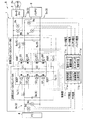
(多入出力電圧変換システムの構成)
図1は多入出力電圧変換システム(多入出力電力変換器を包含)の回路図である。この図1に示すように、多入出力電圧変換システムSは、多入出力電力変換器1にモータINV2と、FC4と、バッテリ6とを接続したものである。多入出力電力変換器1の説明に先立ち、モータINV2、FC4及びバッテリ6について触れておく。
Next, embodiments of the present invention will be described in detail with reference to the drawings as appropriate.
(Configuration of multi-input / output voltage conversion system)
FIG. 1 is a circuit diagram of a multiple input / output voltage conversion system (including a multiple input / output power converter). As shown in FIG. 1, the multi-input / output voltage conversion system S includes a multi-input /
モータINV2は、モータ2aに接続され、このモータ2aに電力を供給するものである。FC4は、車載用の燃料電池であり、後記する動作モードによって、高速運転時と低速運転時とで異なる電圧に昇圧される。バッテリ6は、車載用のバッテリであり、直流12Vの電圧を供給している。
The motor INV2 is connected to the
多入出力電力変換器1は、FC4からバッテリ6に、バッテリ6からFC4に、FC4からモータINV2に、バッテリ6からモータINV2に、モータINV2からバッテリ6に、電圧の昇降を自在に行うものである。なお、昇圧の場合、出力電圧を入力電圧の1倍〜2倍超に昇圧し、降圧の場合、出力電圧を入力電圧の0〜1倍に降圧する。
The multi-input /
この多入出力電力変換器1は、モータINV2に接続される入出力部3a(3)と、FCに接続される入出力部3b(3)と、バッテリ6に接続される入出力部3c(3)と、モータINV2に並列接続される平滑用のコンデンサ5a(5)と、FC4に並列接続される平滑用のコンデンサ(キャパシタ)5b(5)と、バッテリ6に並列接続される平滑用のコンデンサ5c(5)と、FC4に接続されるコイル(インダクタ)L1と、バッテリ6に接続されるコイルL2とを備えている。
The multi-input /
なお、この多入出力電力変換器1は、単に単体DC−DCコンバータを複数組みこんだものではなく、入出力部3に接続されたそれぞれの負荷に対して、昇降圧動作を行う際に、相互依存する複数のコンバータ(電力変換器)から構成されており、これらの電力変換器は切り離せない一塊のものである。
The multi-input /
また、この多入出力電力変換器1は、直列に接続されて共有されているコンデンサ(キャパシタ)C1及びコンデンサC2と、4個のIGBT部7a(7)、IGBT部7b(7)、IGBT部7c(7)及びIGBT部7d(7)とを備えている。
The multi-input /
さらに、この多入出力電力変換器1は、入出力部3aの電流を検出する電流計(電流を検出する検出手段)9a、入出力部3aの電圧を検出する電圧検出器(電圧を検出する検出手段)9b、入出力部3bの電流を検出する電流計9c、入出力部3bの電圧を検出する電圧検出器9d、入出力部3cの電流を検出する電流計9e及び入出力部3cの電圧を検出する電圧検出器9fと、制御部11とを備えている。なお、電流計9a、9c、9e及び電圧検出器9b、9d、9fを一括して、検出手段9と称呼する。
The multi-input /
入出力部3は、入力電圧を印加又は出力電圧を出力する正極側端子(単に、正極側ともいう)と、負極側端子(単に、負極側ともいう)とから構成されている。
平滑用のコンデンサ5は、入出力部3に入力電圧を供給する電源のインピーダンスを下げるために設けられていると共に、入出力部3からの出力電圧が昇圧、回生、導通する際の動作を安定するために取り付けるものである。この実施形態では、この平滑用コンデンサ5は、ケミカルコンデンサとして構成されているが、フィルムコンデンサであってもよい。
The input /
The smoothing
コイルL1、L2は、入出力部3b又は入出力部3cの正極側(又は負極側)に接続されており、IGBT部7のスイッチングにより、入出力部3b又は入出力部3cから供給される電流を、磁気エネルギとして蓄積して、放出電流としてコンデンサC1、C2に供給するものである。
The coils L1 and L2 are connected to the positive electrode side (or negative electrode side) of the input /
コンデンサC1、C2は、入出力部3で共有されており、電荷(電流及び放出電流)を蓄積・放電するものである。このコンデンサC1、C2に蓄積された電荷が入出力部3に放電されることで、入力電圧が昇圧されることになる。
The capacitors C1 and C2 are shared by the input /
IGBT部7は、2個(一対)のIGBT素子(スイッチG1〜G8、フライホイールダイオードD1〜D8を包含)が内蔵されたトランジスタスイッチで、動作モードに従ったスイッチング(オン/オフ)を繰り返すものである。これらIGBT部7は、それぞれ2個(一対)のスイッチ及び2個のフライホイールダイオードを有しており、IGBT部7aはスイッチG1及びスイッチG2とフライホイールダイオードD1及びフライホイールダイオードD2とを、IGBT部7bはスイッチG3及びスイッチG4とフライホイールダイオードD3及びフライホイールダイオードD4とを、IGBT部7cはスイッチG5及びスイッチG6とフライホイールダイオードD5及びフライホイールダイオードD6とを、IGBT部7dはスイッチG7及びスイッチG8とフライホイールダイオードD7及びフライホイールダイオードD8とを有している。なお、この実施形態では、トランジスタスイッチは、IGBT素子であるがこれに限定されるものではない。
The
スイッチG1は、第二入出力部3bの正極側に接続されたコイルL1と、コンデンサC1の正極側とを結ぶ経路に配置されており、この経路の通電をオンオフするものである。
スイッチG2は、第二入出力部3bの正極側に接続されたコイルL1と、コンデンサC1の負極側及びコンデンサC2の正極側とを結ぶ経路に配置されており、この経路の通電をオンオフするものである。
The switch G1 is disposed in a path connecting the coil L1 connected to the positive electrode side of the second input /
The switch G2 is disposed in a path connecting the coil L1 connected to the positive electrode side of the second input /
スイッチG3は、第二入出力部3bの負極側と、コンデンサC1の負極側及びコンデンサC2の正極側とを結ぶ経路に配置されており、この経路の通電をオンオフするものである。
スイッチG4は、第二入出力部3bの負極側と、コンデンサC2の負極側とを結ぶ経路に配置されており、この経路の通電をオンオフするものである。
The switch G3 is disposed in a path connecting the negative electrode side of the second input /
The switch G4 is disposed in a path connecting the negative electrode side of the second input /
スイッチG5は、第三入出力部3cの正極側に接続されたコイルL2と、コンデンサC1の正極側とを結ぶ経路に配置されており、この経路の通電をオンオフするものである。
スイッチG6は、第三入出力部3cの正極側に接続されたコイルL2と、コンデンサC1の負極側及びコンデンサC2の正極側とを結ぶ経路に配置されており、この経路の通電をオンオフするものである。
The switch G5 is disposed in a path connecting the coil L2 connected to the positive electrode side of the third input /
The switch G6 is arranged in a path connecting the coil L2 connected to the positive electrode side of the third input /
スイッチG7は、第三入出力部3cの負極側と、コンデンサC1の負極側及びコンデンサC2の正極側とを結ぶ経路に配置されており、この経路の通電をオンオフするものである。
スイッチG8は、第三入出力部3cの負極側と、コンデンサC2の負極側とを結ぶ経路に配置されており、この経路の通電をオンオフするものである。
The switch G7 is disposed in a path connecting the negative electrode side of the third input /
The switch G8 is disposed in a path connecting the negative electrode side of the third input /
以下、FC4に接続されている入出力部3b、コイルL1、コンデンサ5b、IGBT7a(スイッチG1、スイッチG2)、IGBT7b(スイッチG3、スイッチG4)、コンデンサC1、C2からなる電力変換回路を昇降圧DC−DCコンバータAと称呼し、バッテリ6に接続されている入出力部3c、コイルL2、コンデンサ5c、IGBT7c(スイッチG5、スイッチG6)、IGBT7d(スイッチG7、スイッチG8)、コンデンサC1、C2からなる電力変換回路を昇降圧DC−DCコンバータBと称呼することとする。
Hereinafter, the power conversion circuit including the input /
検出手段9は、入出力部3における電流値及び電圧値を検出するものである。この検出手段9で検出された電流値及び電圧値(検出結果)は、制御部11に入力される。
制御部11は、多入出力電力変換器1の制御を司るもので、検出結果受取手段11aと、検出結果比較手段11bと、動作モード蓄積手段11cと、スイッチング制御手段11dとを備えている。
The detection means 9 detects a current value and a voltage value in the input /
The
検出結果受取手段11aは、検出手段9で検出された電流値及び電圧値(検出結果)を受け取るものである。この検出結果は、モータ電流、モータ電圧、FC電流、FC電圧、バッテリ電流及びバッテリ電圧である。
The detection
検出結果比較手段11bは、検出結果受取手段11aで受け取られた検出結果を比較するもので、比較した結果がスイッチング制御手段11dに出力される。
The detection
動作モード蓄積手段11cは、予め設定した動作モードを蓄積しておくもので、一般的なメモリ等によって構成されている。
スイッチング制御手段11dは、検出結果比較手段11bで比較した結果に基づいて、動作モード蓄積手段11cに蓄積されている動作モード(動作パターン)を読み出してIGBT部7のスイッチングを実行させるものである。
The operation
The switching
この多入出力電力変換器1によれば、制御部11のスイッチング制御手段11dによって、動作モードに従ったIGBT部7(スイッチG1〜G8)のスイッチングが実行され、このスイッチングにより、電流(電荷)をキャパシタに充放電させることで、出力電圧を昇降させており、複数の入出力部3に対し当該コンデンサC1、C2を兼用しているため、当該変換器1の小型軽量化を図ることができる。
According to the multi-input /
また、この多入出力電力変換器1によれば、検出手段9によって、入出力部3それぞれで電圧及び電流を検出し、この検出された電圧及び電流に基づいて、出力電圧の昇降を制御することができる。
Further, according to the multi-input /
次に、多入出力電力変換器1の動作について、図2〜図11を参照して説明する。この多入出力電力変換器1は、IGBT部7の各スイッチG1〜G8のスイッチングによって、昇圧、回生(降圧)、導通の動作を行っている。この場合、昇降圧DC−DCコンバータA、Bは、昇圧回路、降圧回路の役割を果たしている。以下、多入出力電力変換器1の動作の4パターン(その1〜その4)について説明する。
Next, the operation of the multi-input /
(多入出力電力変換器の動作 その1 FCを昇圧[バッテリを昇圧する場合も同様の動作原理])
まず、図2〜図4を参照して、FC4の電圧をモータINV2の電圧に昇圧する動作について説明する。
このFC4の電圧をモータINV2の電圧に昇圧する動作では、IGBT部7aのスイッチG1、IGBT部7bのスイッチG4、IGBT部7c、7dを常時オフとしている。
(Operation of multi-input / output power converter,
First, an operation for boosting the voltage of FC4 to the voltage of motor INV2 will be described with reference to FIGS.
In the operation of boosting the voltage of FC4 to the voltage of the motor INV2, the switch G1 of the
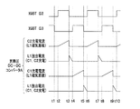
図2は、IGBT部7aのスイッチG2、IGBT部7bのスイッチG3のゲート電圧波形と、コンデンサC1、C2、コイルL1の電流波形とを示した図である。図3(a)は、スイッチG3がオフの状態で、スイッチG2がオンからオフになった際の電流を回路図に示した図である。図3(b)は、スイッチG2がオフの状態で、スイッチG3がオンからオフになった際の電流を回路図に示した図である。図4(a)は、多入出力電力変換器1の電流電圧の実測波形を示した図である。図4(b)は、図4(a)で示した電流電圧の実測波形を計測した箇所を示した図である。
FIG. 2 is a diagram illustrating the gate voltage waveforms of the switch G2 of the
図2に示したように、IGBT部7aのスイッチG2のゲート電圧波形の一周期はt2からt6までであり、IGBT部7bのスイッチG3のゲート電圧波形の一周期はt4からt8までである。
As shown in FIG. 2, one cycle of the gate voltage waveform of the switch G2 of the
そして、IGBT部7aのスイッチG2がオフからオンに切り替わってから、オンからオフに切り替わるまでの期間(t2〜t3、t6〜t7)に、昇降圧DC−DCコンバータAのコンデンサC2において、充電電流が観測され、その際、コイルL1に磁気エネルギが蓄積し、IGBT部7aのスイッチG2がオンからオフに切り替わってから、IGBT部7bのスイッチG3がオフからオンに切り替わるまでの期間(t3〜t4、t7〜t8)に、コイルL1において、放出電流が観測され、それにより、コンデンサC1、C2が充電される。
In the capacitor C2 of the step-up / step-down DC-DC converter A during a period (t2-t3, t6-t7) from when the switch G2 of the
また、IGBT部7bのスイッチG3がオフからオンに切り替わってから、オンからオフに切り替わるまでの期間(t4〜t5、t8〜t9)に、昇降圧DC−DCコンバータAのコンデンサC1において、充電電流が観測され、その際、コイルL1に磁気エネルギが蓄積し、IGBT部7bのスイッチG3がオンからオフに切り替わってから、IGBT部7aのスイッチG2がオフからオンに切り替わるまでの期間(t5〜t6、t9〜t10)に、コイルL1において、放出電流が観測され、それにより、コンデンサC1、C2が充電される。
Further, in the capacitor C1 of the step-up / step-down DC-DC converter A during the period (t4 to t5, t8 to t9) from when the switch G3 of the
つまり、IGBT部7aのスイッチG2がオフからオン又はIGBT部7bのスイッチG3がオフからオンに切り替わることで、コンデンサC1とコンデンサC2とがFC4により交互に充電されると共に、この際にコイルL1に蓄積された磁気エネルギによる放出電流もコンデンサC1及びコンデンサC2に充電されるという昇圧動作がなされ、FC4の電圧(入力電圧)がモータINV2の電圧(出力電圧)に昇圧されることになる。
That is, when the switch G2 of the
なお、ここでは、昇降圧DC−DCコンバータAによって昇圧動作を行って、FC4の電圧をモータINV2の電圧に昇圧させているが、昇降圧DC−DCコンバータBによって昇圧動作を行えば、バッテリ6の電圧をモータINV2の電圧に昇圧させることも可能である。ちなみに、これらスイッチG2とスイッチG3のオン時間のデューティー比を50%以上にすれば、FC電圧とモータ電圧との昇圧比を2倍以上にすることができる。 Here, the step-up / step-down DC-DC converter A boosts the voltage of the FC4 to boost the voltage of the motor INV2, but if the step-up / step-down DC-DC converter B boosts the voltage, the battery 6 Can be boosted to the voltage of the motor INV2. Incidentally, if the duty ratio of the ON time of these switches G2 and G3 is set to 50% or more, the step-up ratio between the FC voltage and the motor voltage can be doubled or more.
この場合、図3(a)、図3(b)に示したように、多入出力電力変換器1の各経路で電流が流れる。この図3(a)、図3(b)において、点線I1(C2充電電流)、I2(L1放出電流)及びI3(C1充電電流)がFC電流を表し、点線I4がモータ電流を表している。
In this case, current flows through each path of the multi-input /
図3(a)に示した点線I1(C2充電電流)は、IGBT部7aのスイッチG2がオンの期間(t2〜t3、t6〜t7)に、入出力部3bの正極側からコイルL1、IGBT部7aのスイッチG2に流れ、このIGBT部7aのスイッチG2を経由して、コンデンサC2にて蓄積される。
The dotted line I1 (C2 charging current) shown in FIG. 3A indicates that the coil L1 and IGBT from the positive electrode side of the input /
図3(a)に示した点線I2(L1放出電流)は、IGBT部7aのスイッチG2がオフ及びIGBT部7bのスイッチG3がオフの期間(t3〜t4、t7〜t8)に、入出力部3bの正極側からコイルL1、IGBT部7aのフライホイールダイオードD1に流れ、このIGBT部7aのフライホイールダイオードD1を経由して、コンデンサC1、コンデンサC2にて一挙に蓄積される。
The dotted line I2 (L1 emission current) shown in FIG. 3A indicates the input / output unit during a period (t3 to t4, t7 to t8) in which the switch G2 of the
図3(b)に示した点線I3(C1充電電流)は、IGBT部7bのスイッチG3がオンの期間(t4〜t5、t8〜t9)に、入出力部3bの正極側からコイルL1、IGBT部7aのフライホイールダイオードD1に流れ、このIGBT部7aのフライホイールダイオードD1を経由して、コンデンサC1にて蓄積される。
The dotted line I3 (C1 charging current) shown in FIG. 3B indicates that the coil L1 and IGBT from the positive electrode side of the input /
図3(a)に示した点線I4(モータ電流)は、コンデンサC1及びコンデンサC2に蓄積された電荷がモータINV2に流れる電流を表している。
そして、図4(a)に示したように、電流電圧の実測波形が得られる。この図4(a)の符号a1が示す実測波形は、スイッチG2をオンオフするためのゲート電圧波形であり、符号a2が示す実測波形は、入出力部3bの正極側に流れる電流波形である。また、図4(a)の符号a3が示す実測波形は、スイッチG2を流れる電流波形であり、符号a4が示す実測波形は、スイッチG1とコンデンサC1とを結ぶ経路に流れる電流波形である。
A dotted line I4 (motor current) shown in FIG. 3A represents a current in which charges accumulated in the capacitor C1 and the capacitor C2 flow to the motor INV2.
Then, as shown in FIG. 4A, a measured waveform of the current voltage is obtained. The measured waveform indicated by reference sign a1 in FIG. 4A is a gate voltage waveform for turning on / off the switch G2, and the measured waveform indicated by reference sign a2 is a current waveform flowing on the positive electrode side of the input /
なお、図4(b)では、V1がFC電圧を、V2がモータ電圧を示しており、図4(a)に対応した符号a1、a2、a3、a4を付している。これらの実測波形から、前記したように、FC電圧が昇圧されることを確認することができる。 In FIG. 4B, V1 indicates the FC voltage and V2 indicates the motor voltage, and reference numerals a1, a2, a3, and a4 corresponding to FIG. From these measured waveforms, as described above, it can be confirmed that the FC voltage is boosted.
(多入出力電力変換器の動作 その2 モータINVを降圧[回生])
次に、図5〜図7を参照して、モータINV2の電圧をバッテリ6の電圧に降圧(回生)する動作について説明する。
このモータINV2の電圧をバッテリ6の電圧に降圧する動作では、IGBT部7a、IGBT部7b、IGBT部7cのスイッチG6、IGBT部7dのスイッチG7を常時オフとしている。また、この場合、IGBT部7cのフライホイールダイオードD6及びIGBT部7dのフライホイールダイオードD7が順方向の電流を流す作用をしている。この動作は、降圧率が低い(0.5〜1倍)場合(回生負荷が小さい場合)のものである。
(Operation of multi-input / output
Next, the operation of stepping down (regenerating) the voltage of the motor INV2 to the voltage of the battery 6 will be described with reference to FIGS.
In the operation of stepping down the voltage of the motor INV2 to the voltage of the battery 6, the
図5は、IGBT部7cのスイッチG5、IGBT部7dのスイッチG8のゲート電圧波形と、コンデンサC1、C2、コイルL2の電流波形とを示した図である。図6(a)は、スイッチG5及びスイッチG8がオンの状態から、スイッチG8がオンからオフになった際の電流を回路図に示した図である。図6(b)は、スイッチG5及びスイッチG8がオンの状態から、スイッチG5がオンからオフになった際の電流を回路図に示した図である。図7(a)は、多入出力電力変換器1の電流電圧の実測波形を示した図である。図7(b)は、図7(a)で示した電流電圧の実測波形を計測した箇所を示した図である。
FIG. 5 is a diagram showing the gate voltage waveforms of the switch G5 of the
図5に示したように、IGBT部7cのスイッチG5のゲート電圧波形の一周期はt1からt5までであり、IGBT部7dのスイッチG8のゲート電圧波形の一周期はt3からt7までである。そして、これらのゲート電圧波形のt1〜t2、t3〜t4、t5〜t6、t7〜t8、t9〜t10はIGBT部7cのスイッチG5及びIGBT部7dのスイッチG8が同時にオンになる期間(同時オン期間)である。
As shown in FIG. 5, one cycle of the gate voltage waveform of the switch G5 of the
また、ゲート電圧波形のt2〜t3、t6〜t7は、IGBT部7cのスイッチG5のみがオンの期間である。さらに、ゲート電圧波形のt4〜t5、t8〜t9は、IGBT部7dのスイッチG8のみがオンの期間である。このように、IGBT部7cのスイッチG5及びIGBT部7dのスイッチG8が交互にオンオフされる間に、同時オン期間が介在するように、制御部11(図1参照)がゲート電圧を制御する。
Also, t2 to t3 and t6 to t7 of the gate voltage waveform are periods in which only the switch G5 of the
同時オン期間では、IGBT部7cのスイッチG5及びIGBT部7dのスイッチG8が同時にオンになり、モータINV2からコンデンサC1及びコンデンサC2に充電電流(図6、I4)が流れ、一方、モータINV2とコンデンサC1及びコンデンサC2からコイルL2に電流(図6、I5)が流れることにより、コイル2にエネルギが蓄積される。これによって、モータINV2からコンデンサC1及びコンデンサC2の直列放電によりコイルL2に大きな電流を流すことができ、コイルL2の開放電流を同時オンでない期間に断続することなく流すことができる。
In the simultaneous ON period, the switch G5 of the
そして、ゲート電圧波形のt2〜t3、t6〜t7は、IGBT部7cのスイッチG5のみがオンの期間(IGBT部7dのスイッチG8はオフ、コンデンサC1の放出期間)では、IGBT部7dのフライホイールダイオードD7が導通状態となって、コイルL2に蓄積されていた磁気エネルギの放出電流(図6、I6)がコンデンサ5cを充電するとともに、バッテリ6を充電する。また、コイルL2の磁気エネルギの放出時にコイルL2の両端には電圧が発生し、この電圧により、バッテリ電圧とコンデンサC1との電圧差を補い、電流を流し続けることができる。
The gate voltage waveforms t2 to t3 and t6 to t7 are flywheels of the
そして、ゲート電圧波形のt4〜t5、t8〜t9は、IGBT部7dのスイッチG8のみがオンの期間(IGBT部7cのスイッチG5はオフ、コンデンサC2の放出期間)では、IGBT部7cのフライホイールダイオードD6が導通状態となって、コイルL2に蓄積されていた磁気エネルギの放出電流(図6、I7)がコンデンサ5cを充電するとともに、バッテリ6を充電する。また、コイルL2の磁気エネルギの放出時にコイルL2の両端には電圧が発生し、この電圧により、バッテリ電圧とコンデンサC2との電圧差を補い、電流を流し続けることができる。
Then, t4 to t5 of the gate voltage waveform, T8~t 9 is, in the period only the switch G8 is on of the
そして、図7(a)に示したように、電流電圧の実測波形が得られる。この図7(a)の符号a1が示す実測波形は、スイッチG8をオンオフするためのゲート電圧波形であり、符号a2が示す実測波形は、入出力部3cの正極側に流れる電流波形である。また、図7(a)の符号a3が示す実測波形は、スイッチG5を流れる電流波形であり、符号a4が示す実測波形は、コンデンサC1とコンデンサC2の接続部を流れる電流波形である。
Then, as shown in FIG. 7A, a measured waveform of the current voltage is obtained. The measured waveform indicated by reference sign a1 in FIG. 7A is a gate voltage waveform for turning on / off the switch G8, and the measured waveform indicated by reference sign a2 is a current waveform flowing on the positive electrode side of the input /
(多入出力電力変換器の動作 その3 FCを昇圧、モータINVを降圧、バッテリを充電)
次に、図8、図9を参照して、FC4の電圧をモータINV2の電圧に昇圧し、モータINV2の電圧を降圧して、バッテリ6を充電する動作について説明する。
このFC4の昇圧、モータINV2を降圧、バッテリ6を充電する動作では、IGBT部7aのスイッチG1、IGBT部7bのスイッチG4、IGBT部7cのスイッチG6、IGBT部7dのスイッチG7を常時オフとしている。
(Operation of multi-input / output
Next, an operation for charging the battery 6 by boosting the voltage of the FC4 to the voltage of the motor INV2 and lowering the voltage of the motor INV2 will be described with reference to FIGS.
In the operation of boosting FC4, stepping down the motor INV2, and charging the battery 6, the switch G1 of the
図8は、IGBT部7aのスイッチG2、IGBT部7bのスイッチG3、IGBT7cのスイッチG5、IGBT7dのスイッチG8のゲート電圧波形と、昇降圧DC−DCコンバータAのC2充電電流、L1放出電流、C1充電電流の波形と、昇降圧DC−DCコンバータBのC1、C2充電電流、C1放出電流、C2放出電流の波形とを示した図である。
FIG. 8 shows the gate voltage waveform of the switch G2 of the
図9(a)は、スイッチG3がオフの状態で、スイッチG2がオンからオフになった際、且つ、スイッチG5及びスイッチG8がオンの状態で、スイッチG8がオフになった際の電流を回路図に示した図である。図9(b)は、スイッチG2がオフの状態で、スイッチG3がオンからオフになった際、且つ、スイッチG5及びスイッチG8がオンの状態で、スイッチG5がオフになった際の電流を回路図に示した図である。 FIG. 9A shows the current when the switch G3 is turned off and the switch G2 is turned off, and when the switch G5 and the switch G8 are turned on and the switch G8 is turned off. It is the figure shown to the circuit diagram. FIG. 9B shows the current when the switch G2 is turned off while the switch G3 is turned off, and when the switch G5 and the switch G8 are turned on and the switch G5 is turned off. It is the figure shown to the circuit diagram.
図8に示したように、IGBT部7aのスイッチG2のゲート電圧波形の一周期はt2からt10までであり、IGBT部7bのスイッチG3のゲート電圧波形の一周期はt6からt14までであり、IGBT部7cのスイッチG5のゲート電圧波形の一周期はt3からt11までであり、IGBT部7dのスイッチG8のゲート電圧波形の一周期はt7からt15までである。
As shown in FIG. 8, one cycle of the gate voltage waveform of the switch G2 of the
そして、IGBT部7aのスイッチG2がオフからオンに切り替わってから、オンからオフに切り替わるまでの期間(t2〜t5、t10〜t13)に、昇降圧DC−DCコンバータAのコンデンサC2において、充電電流が観測され、その際、コイルL1に磁気エネルギが蓄積し、IGBT部7aのスイッチG2がオンからオフに切り替わってから、IGBT部7bのスイッチG3がオフからオンに切り替わるまでの期間(t5〜t6、t13〜t14)に、コイルL1において、放出電流が観測され、それにより、コンデンサC1、C2が充電される。
Then, in the capacitor C2 of the step-up / step-down DC-DC converter A during the period (t2-t5, t10-t13) from when the switch G2 of the
また、IGBT部7bのスイッチG3がオンからオフに切り替わってから、オンからオフに切り替わるまでの期間(〜t1、t6〜t9、t14〜t17)に、昇降圧DC−DCコンバータAのコンデンサC1において、充電電流が観測され、その際、コイルL1に磁気エネルギが蓄積し、IGBT部7bのスイッチG3がオンからオフに切り替わってから、IGBT部7aのスイッチG2がオフからオンに切り替わるまでの期間(t1〜t2、t9〜t10、t17〜t18)に、コイルL1において、放出電流が観測され、それにより、コンデンサC1、C2が充電される。
Further, in the capacitor C1 of the step-up / step-down DC-DC converter A during the period from when the switch G3 of the
つまり、IGBT部7aのスイッチG2がオフからオン又はIGBT部7bのスイッチG3がオフからオンに切り替わることで、コンデンサC1とコンデンサC2とがFC4により交互に充電されると共に、この際にコイルL1に蓄積された磁気エネルギによる放出電流もコンデンサC1とコンデンサC2とに充電されるという昇圧動作がなされ、FC4の電圧(入力電圧)がモータINV2の電圧(出力電圧)に昇圧されることになる。すなわち、IGBT部7aのスイッチG2及びIGBT部7bのスイッチG3のスイッチングを交互に行うことにより、FC4によりコンデンサC1及びコンデンサC2を交互に充電すると共に、コイルL1の開放電流によりコンデンサC1及びコンデンサC2を充電することができるので、電流の断続なく昇圧動作を行うことができる。
That is, when the switch G2 of the
また、IGBT部7cのスイッチG5及びIGBT部7dのスイッチG8が同時にオンになっている期間(同時オン期間、t3〜t4、t7〜t8、t11〜t12、t15〜t16)は、昇降圧DC−DCコンバータBのコンデンサC1、コンデンサC2において、充電電流が観測され、その際、コイルL2に磁気エネルギが蓄積し、IGBT部7cのスイッチG5がオンからオフに切り替わった場合(t8、t16)、昇降圧DC−DCコンバータBのコンデンサC2において、放出電流が観測され、IGBT部7dのスイッチG8がオンからオフに切り替わった場合(t4、t12)、昇降圧DC−DCコンバータBのコンデンサC1において、放出電流が観測される。
Further, during the period in which the switch G5 of the
このようにして、コンデンサC1及びコンデンサC2の放出電流(回生電力)がバッテリ6側に返還され、コンデンサC1及びコンデンサC2の電圧が降下する。つまり、モータINV2の電圧(入力電圧)がバッテリ6の電圧(出力電圧)に降圧されることになる。 In this way, the discharge current (regenerative power) of the capacitors C1 and C2 is returned to the battery 6 side, and the voltages of the capacitors C1 and C2 drop. That is, the voltage (input voltage) of the motor INV2 is stepped down to the voltage (output voltage) of the battery 6.
図9(a)に示した点線I1(C2充電電流)は、IGBT部7aのスイッチG2がオンの期間(t2〜t5、t10〜t13)に、入出力部3bの正極側からコイルL1、IGBT部7aのスイッチG2に流れ、このIGBT部7aのスイッチG2を経由して、コンデンサC2にて蓄積される。
The dotted line I1 (C2 charging current) shown in FIG. 9A indicates that the coil L1 and IGBT from the positive electrode side of the input /
図9(a)に示した点線I2(L1放出電流)は、IGBT部7aのスイッチG2がオフ及びIGBT部7bのスイッチG3がオフの期間(t1〜t2、t5〜t6、t9〜t10、t13〜t14、t17〜t18)に、入出力部3bの正極側からコイルL1、IGBT部7aのフライホイールダイオードD1に流れ、このIGBT部7aのフライホイールダイオードD1を経由して、コンデンサC1、コンデンサC2にて一挙に蓄積される。
A dotted line I2 (L1 emission current) shown in FIG. 9A indicates a period (t1-t2, t5-t6, t9-t10, t13) in which the switch G2 of the
図9(b)に示した点線I3(C1充電電流)は、IGBT部7bのスイッチG3がオンの期間(t6〜t9、t14〜t17)に、入出力部3bの正極側からコイルL1、IGBT部7aのフライホイールダイオードD1に流れ、このIGBT部7aのフライホイールダイオードD1を経由して、コンデンサC1にて蓄積される。
The dotted line I3 (C1 charging current) shown in FIG. 9B indicates that the coil L1 and IGBT from the positive electrode side of the input /
図9(a)に示した点線I4(モータ電流)は、コンデンサC1及びコンデンサC2に蓄積された電荷がモータINV2に流れる電流を表している。 A dotted line I4 (motor current) shown in FIG. 9A represents a current in which charges accumulated in the capacitor C1 and the capacitor C2 flow to the motor INV2.
図9(a)に示した点線I5(C1、C2放電電流)は、IGBT部7cのスイッチG5及びIGBT部7dのスイッチG8がオンの期間(t3〜t4、t7〜t8、t11〜t12、t15〜t16)に、コンデンサC1からIGBT部7cのスイッチG5を経由して、コイルL2に磁気エネルギを蓄積しながら、コンデンサ5c、IGBT部7dのスイッチG8を経由して、コンデンサC2に流れる。
A dotted line I5 (C1, C2 discharge current) shown in FIG. 9A indicates a period (t3 to t4, t7 to t8, t11 to t12, and the switch G5 of the
図9(a)に示した点線I6(C1放出電流)は、IGBT部7cのスイッチG5及びIGBT部7dのスイッチG8がオンの期間において、IGBT部7dのスイッチG8がオンからオフに切り替わった瞬間から再びスイッチG8がオンになるまでの期間(t4〜t7、t12〜t15)に、コンデンサC1からIGBT部7cのスイッチG5、コイルL2、コンデンサ5c、IGBT部7dのフライホイールダイオードD7を経由して、コンデンサC1に流れる。
The dotted line I6 (C1 emission current) shown in FIG. 9A represents the moment when the switch G8 of the
図9(b)に示した点線I7(C2放出電流)は、IGBT部7cのスイッチG5及びIGBT部7dのスイッチG8がオンの期間において、IGBT部7cのスイッチG5がオンからオフに切り替わった瞬間から再びスイッチG5がオンになるまでの期間(〜t3、t8〜t11、t16〜)に、コンデンサC2からIGBT部7cのフライホイールダイオードD6、コイルL2、コンデンサ5c、IGBT部7dのスイッチG8を経由して、コンデンサC2に流れる。
The dotted line I7 (C2 emission current) shown in FIG. 9B indicates the moment when the switch G5 of the
(多入出力電力変換器の動作 その4 FCを昇圧、バッテリを昇圧)
次に、図10、図11を参照して、FC4の電圧をモータINV2の電圧に昇圧し、バッテリ6の電圧を昇圧する動作について説明する。
このFC4の昇圧、バッテリ6の昇圧をする動作では、IGBT部7aのスイッチG1、IGBT部7bのスイッチG4、IGBT部7cのスイッチG5、IGBT部7dのスイッチG8を常時オフとしている。
(Operation of multi-input / output power converter, Part 4: Boost FC and boost battery)
Next, an operation for boosting the voltage of the FC4 to the voltage of the motor INV2 and boosting the voltage of the battery 6 will be described with reference to FIGS.
In the operation of boosting the FC4 and boosting the battery 6, the switch G1 of the
図10は、IGBT部7aのスイッチG2、IGBT部7bのスイッチG3、IGBT7cのスイッチG6、IGBT7dのスイッチG7のゲート電圧波形と、昇降圧DC−DCコンバータAのC2充電電流、L1放出電流、C1充電電流の波形と、昇降圧DC−DCコンバータBのC2充電電流、L2放出電流、C1充電電流の波形とを示した図である。
FIG. 10 shows the gate voltage waveform of the switch G2 of the
図11(a)は、スイッチG3がオフの状態で、スイッチG2がオンからオフになった際、且つ、スイッチG7がオフの状態で、スイッチG6がオンからオフになった際の電流を回路図に示した図である。図11(b)は、スイッチG2がオフの状態で、スイッチG3がオンからオフになった際、且つ、スイッチG6がオフの状態で、スイッチG7がオンからオフになった際の電流を回路図に示した図である。 FIG. 11A is a circuit diagram illustrating the current when the switch G3 is turned off from the on state when the switch G3 is turned off, and when the switch G6 is turned off from the on state when the switch G7 is turned off. It is the figure shown in the figure. FIG. 11B shows the current when the switch G2 is turned off and the switch G3 is turned off, and when the switch G6 is turned off and the switch G7 is turned off. It is the figure shown in the figure.
図10に示したように、IGBT部7aのスイッチG2のゲート電圧波形の一周期はt3からt11までであり、IGBT部7bのスイッチG3のゲート電圧波形の一周期はt7からt15までであり、IGBT部7cのスイッチG6のゲート電圧波形の一周期はt6からt14までであり、IGBT部7dのスイッチG7のゲート電圧波形の一周期はt2からt10までである。
As shown in FIG. 10, one period of the gate voltage waveform of the switch G2 of the
そして、IGBT部7aのスイッチG2がオフからオンに切り替わってから、オンからオフに切り替わるまでの期間(t3〜t6、t11〜t14)に、昇降圧DC−DCコンバータAのコンデンサC2において、充電電流が観測され、その際、コイルL1に磁気エネルギが蓄積し、IGBT部7aのスイッチG2がオンからオフに切り替わってから、IGBT部7bのスイッチG3がオフからオンに切り替わるまでの期間(t6〜t7、t14〜t15)に、コイルL1において、放出電流が観測され、それにより、コンデンサC1、C2が充電される。
Then, during the period (t3 to t6, t11 to t14) from when the switch G2 of the
また、IGBT部7bのスイッチG3がオフからオンに切り替わってから、オンからオフに切り替わるまでの期間(t7〜t10、t15〜t18)に、昇降圧DC−DCコンバータAのコンデンサC1において、充電電流が観測され、その際、コイルL1に磁気エネルギが蓄積し、IGBT部7bのスイッチG3がオンからオフに切り替わってから、IGBT部7aのスイッチG2がオフからオンに切り替わるまでの期間(t2〜t3、t10〜t11、t18〜t19)に、コイルL1において、放出電流が観測され、それにより、コンデンサC1、C2が充電される。
Further, in the capacitor C1 of the step-up / step-down DC-DC converter A during a period (t7 to t10, t15 to t18) from when the switch G3 of the
つまり、IGBT部7aのスイッチG2がオフからオン又はIGBT部7bのスイッチG3がオフからオンに切り替わることで、コンデンサC1とコンデンサC2とがFC4により交互に充電されると共に、この際にコイルL1に蓄積された磁気エネルギによる放出電流もコンデンサC1及びコンデンサC2に充電されるという昇圧動作がなされ、FC4の電圧(入力電圧)がモータINV2の電圧(出力電圧)に昇圧されることになる。
That is, when the switch G2 of the
同様に、IGBT部7cのスイッチG6がオフからオンに切り替わってから、オンからオフに切り替わるまでの期間(t6〜t9、t14〜t17)に、昇降圧DC−DCコンバータBのコンデンサC2において、充電電流が観測され、その際、コイルL2に磁気エネルギが蓄積し、IGBT部7cのスイッチG6がオンからオフに切り替わってから、IGBT部7dのスイッチG7がオフからオンに切り替わるまでの期間(t9〜t10、t17〜t18)に、コイルL2において、放出電流が観測され、それにより、コンデンサC1、C2が充電される。
Similarly, charging is performed in the capacitor C2 of the step-up / step-down DC-DC converter B during a period (t6 to t9, t14 to t17) from when the switch G6 of the
また、IGBT部7dのスイッチG7がオフからオンに切り替わってから、オンからオフに切り替わるまでの期間(t2〜t5、t10〜t13)に、昇降圧DC−DCコンバータBのコンデンサC1において、充電電流が観測され、その際、コイルL2に磁気エネルギが蓄積し、IGBT部7dのスイッチG7がオンからオフに切り替わってから、IGBT部7cのスイッチG6がオフからオンに切り替わるまでの期間(t5〜t6、t13〜t14)に、コイルL2において、放出電流が観測され、それにより、コンデンサC1、C2が充電される。
Further, in the capacitor C1 of the step-up / step-down DC-DC converter B during a period (t2-t5, t10-t13) from when the switch G7 of the
つまり、IGBT部7cのスイッチG6がオフからオン又はIGBT部7dのスイッチG7がオフからオンに切り替わることで、コンデンサC1とコンデンサC2とがFC4により交互に充電されると共に、この際にコイルL2に蓄積された磁気エネルギによる放出電流もコンデンサC1及びコンデンサC2に充電されるという昇圧動作がなされ、バッテリ6の電圧(入力電圧)がモータINV2の電圧(出力電圧)に昇圧されることになる。
That is, when the switch G6 of the
図11(a)に示した点線I1(C2充電電流)は、IGBT部7aのスイッチG2がオンの期間(t3〜t6、t11〜t14)に、入出力部3bの正極側からコイルL1、IGBT部7aのスイッチG2に流れ、このIGBT部7aのスイッチG2を経由して、コンデンサC2にて蓄積される。
The dotted line I1 (C2 charging current) shown in FIG. 11A indicates that the coil L1 and IGBT from the positive electrode side of the input /
図11(a)に示した点線I2(L1放出電流)は、IGBT部7aのスイッチG2がオフ及びIGBT部7bのスイッチG3がオフの期間(t2〜t3、t6〜t7、t10〜t11、t14〜t15、t18〜t19)に、入出力部3bの正極側からコイルL1、IGBT部7aのフライホイールダイオードD1に流れ、このIGBT部7aのフライホイールダイオードD1を経由して、コンデンサC1、コンデンサC2にて一挙に蓄積される。
A dotted line I2 (L1 emission current) shown in FIG. 11A indicates a period (t2 to t3, t6 to t7, t10 to t11, t14) in which the switch G2 of the
図11(b)に示した点線I3(C1充電電流)は、IGBT部7bのスイッチG3がオンの期間(〜t2、t7〜t10、t15〜t18)に、入出力部3bの正極側からコイルL1、IGBT部7aのフライホイールダイオードD1に流れ、このIGBT部7aのフライホイールダイオードD1を経由して、コンデンサC1にて蓄積される。
The dotted line I3 (C1 charging current) shown in FIG. 11 (b) indicates that the coil from the positive electrode side of the input /
図11(a)に示した点線I4(モータ電流:交流電流)は、入出力部3aの上側からコンデンサC1及びコンデンサC2を経由して、入出力部3aの下側に流れる。図11(b)に示した点線I4(モータ電流:交流電流)は、入出力部3aの下側からコンデンサC2及びコンデンサC1を経由して、入出力部3aの上側に流れる。
A dotted line I4 (motor current: alternating current) shown in FIG. 11A flows from the upper side of the input /
図11(a)に示した点線I8(C2充電電流)は、IGBT部7cのスイッチG6がオンの期間(t6〜t9、t14〜t17)に、入出力部3cの正極側からコイルL2、IGBT部7cのスイッチG6に流れ、このIGBT部7cのスイッチG6を経由して、コンデンサC2にて蓄積される。
A dotted line I8 (C2 charging current) shown in FIG. 11A indicates that the coil L2 and the IGBT L2 from the positive electrode side of the input /
図11(a)に示した点線I9(L1放出電流)は、IGBT部7cのスイッチG6がオフ及びIGBT部7dのスイッチG7がオフの期間(t5〜t6、t9〜t10、t13〜t14、t17〜t18)に、入出力部3cの正極側からコイルL2、IGBT部7cのフライホイールダイオードD5に流れ、このIGBT部7cのフライホイールダイオードD5を経由して、コンデンサC1、コンデンサC2にて一挙に蓄積される。
A dotted line I9 (L1 emission current) shown in FIG. 11A indicates a period (t5 to t6, t9 to t10, t13 to t14, t17) in which the switch G6 of the
図11(b)に示した点線I10(C1充電電流)は、IGBT部7dのスイッチG7がオンの期間(t2〜t5、t10〜t13、t18〜)に、入出力部3cの正極側からコイルL2、IGBT部7cのフライホイールダイオードD5に流れ、このIGBT部7cのフライホイールダイオードD5を経由して、コンデンサC1にて蓄積される。
The dotted line I10 (C1 charging current) shown in FIG. 11B is a coil from the positive electrode side of the input /
なお、この図11において、昇降圧DC−DCコンバータAと昇降圧DC−DCコンバータBを、タイミングをずらして動作させると、I1、I2、I8、I9とI2、I3、I9、I10の電流が同時に流れないので、コンデンサC1及びコンデンサC2に対する負荷を低減でき、容量を小さくすることができる。 In FIG. 11, when the step-up / step-down DC-DC converter A and the step-up / step-down DC-DC converter B are operated at different timings, the currents I1, I2, I8, I9 and I2, I3, I9, I10 are Since they do not flow at the same time, the load on the capacitor C1 and the capacitor C2 can be reduced, and the capacitance can be reduced.
(多入出力電力変換器の動作、導通)
多入出力電力変換器1のIGBT部7a及びIGBT7bのすべてのスイッチG1〜スイッチG4を常時オフ(停止)にしIGBT部7c及びIGBT7dのすべてのスイッチG5〜スイッチG8を常時オンにする(又はIGBT部7a及びIGBT7bのすべてのスイッチG1〜スイッチG4を常時オンにしIGBT部7c及びIGBT7dのすべてのスイッチG5〜スイッチG8を常時オフ(停止)にする)と、通常の整流回路(導通回路:1倍の昇圧回路)として動作することになる。
(Operation of multi-input / output power converter, conduction)
All the switches G1 to G4 of the
この場合、入出力部3bの正極側からコイルL1、IGBT部7aのフライホイールダイオードD1、IGBT部7cのスイッチG5、コイルL2を経由して、入出力部3cに電流が流れ、さらに、入出力部3cの正極側から負極側、IGBT7dのスイッチG8、IGBT部7bのフライホイールダイオードD4を経由して、入出力部3bの負極側に電流が流れ、コンデンサC1、コンデンサC2は昇圧(降圧)には寄与しない。
In this case, a current flows from the positive electrode side of the input /
(多入出力電力変換器の応用例)
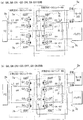
次に、図12を参照して、多入出力電力変換器1の応用例について説明する。
図12に示したように、多入出力電力変換器1の応用例は、電力変換回路(DC−DCコンバータC、D)が共有されている直列コンデンサ(キャパシタ)C1及びコンデンサC2を、さらに他の電力変換回路(DC−DCコンバータE、F)と共有し、一方(上側)の一つの電力変換器(DC−DCコンバータC)のスイッチG1及びスイッチG4を省略すると共に、他方(下側)の電力変換回路(DC−DCコンバータE、F)の入出力部3aを省略したものである。
(Application example of multi-input / output power converter)
Next, an application example of the multi-input /
As shown in FIG. 12, the application example of the multi-input /
電力変換回路(DC−DCコンバータC)は、スイッチG1及びスイッチG4を省略しており、昇圧動作のみが可能であり、電力変換回路(DC−DCコンバータD)は、昇降圧動作が可能である。また、電力変換回路(DC−DCコンバータE、F)は、降圧動作のみが可能である。それぞれの負荷(A/C:エアコン、A/P:補機)に対して、降圧動作のみを行うことができる。 The power conversion circuit (DC-DC converter C) omits the switch G1 and the switch G4, and can perform only a boosting operation. The power conversion circuit (DC-DC converter D) can perform a step-up / step-down operation. . Further, the power conversion circuit (DC-DC converters E and F) can only perform a step-down operation. Only the step-down operation can be performed for each load (A / C: air conditioner, A / P: auxiliary machine).
このように、多入出力電力変換器1の応用例では、複数の電力変換回路(DC−DCコンバータC、D、E、F)に、直列に接続させたコンデンサC1及びコンデンサC2が共有されることで、電力変換回路をコンパクトにし、複数の入出力の電力制御を行うことが可能である。
As described above, in the application example of the multi-input /
また、この応用例に限らず、本発明は、太陽電池システムのように、複数の電源負荷と接続する場合も一つの多入出力電力変換器1により昇降圧動作が行えるため、当該システムの小型化の面で好適である。この場合、共有されているコンデンサの容量は接続する太陽電池の容量・数量等に応じて適宜設定される。
Further, the present invention is not limited to this application example, and the present invention can perform a step-up / step-down operation by a single multi-input /
以上、本発明の実施形態について説明したが、本発明は前記実施形態には限定されない。例えば、昇圧動作又は降圧動作のみしか行わない負荷を接続する場合等、昇降圧動作に関係しないスイッチを常時停止としているが、動作に関係していないスイッチを省略することも可能である。また、複数の電力変換回路(昇降圧DC−DCコンバータA、B、DC−DCコンバータC、D、E、F)において、個々の昇降圧動作をさせるときに、共有しているキャパシタ(コンデンサC1及びコンデンサC2)に対する電力変換回路の動作タイミング(スイッチング)をずらすことが望ましい。ただし、2倍超の昇圧動作、降圧率が0.5〜1の降圧動作の場合には、各電力変換回路のスイッチを同時にスイッチングさせることも可能である。 As mentioned above, although embodiment of this invention was described, this invention is not limited to the said embodiment. For example, when a load that performs only a boosting operation or a step-down operation is connected, a switch not related to the step-up / step-down operation is always stopped, but a switch not related to the operation can be omitted. In addition, when a plurality of power conversion circuits (step-up / step-down DC-DC converters A and B, DC-DC converters C, D, E, and F) perform individual step-up / step-down operations, a shared capacitor (capacitor C1) It is desirable to shift the operation timing (switching) of the power conversion circuit with respect to the capacitor C2). However, in the case of a step-up operation exceeding twice and a step-down operation with a step-down rate of 0.5 to 1, it is possible to simultaneously switch the switches of each power conversion circuit.
なお、動作タイミングをずらすのは、共有している直列のコンデンサC1及びコンデンサC2(共有コンデンサ)への負担を減らすためである。すなわち、複数の電力変換回路の個々の昇降圧動作のスイッチングタイミングをずらすことにより、共有コンデンサに対する負担が低減でき、容量の小さいコンデンサを用いることができる。 The reason for shifting the operation timing is to reduce the burden on the shared series capacitor C1 and capacitor C2 (shared capacitor). That is, by shifting the switching timing of each step-up / step-down operation of the plurality of power conversion circuits, the burden on the shared capacitor can be reduced, and a capacitor having a small capacity can be used.
また、この多入出力電力変換器1を、モータ駆動電力を供給する電動機、燃料電池及びバッテリを備えた燃料電池車に搭載し、当該電動機と多入出力電力変換器1の入出力部3aとを接続することも可能である。この場合、モータ駆動電力と燃料電池又はバッテリの回生電力とのやりとりが頻繁に行われるため、多入出力電力変換器1を利用することで、変換損失の少ないシステムを実現することができる。
The multi-input /
1 多入出力電力変換器
3(3a、3b、3c) 入出力部
5(5a、5b、5c) コンデンサ(平滑用のコンデンサ)
7(7a、7b、7c、7d) IGBT部
9(9a、9b、9c、9d、9e、9f) 検出手段
11 制御部
G1〜G8 スイッチ
D1〜D8 フライホイールダイオード
L1、L2 コイル(インダクタ)
C1,C2 コンデンサ(キャパシタ)
1 Multi-input / output power converter 3 (3a, 3b, 3c) Input / output unit 5 (5a, 5b, 5c) Capacitor (capacitor for smoothing)
7 (7a, 7b, 7c, 7d) IGBT unit 9 (9a, 9b, 9c, 9d, 9e, 9f) Detection means 11 Control unit G1-G8 Switch D1-D8 Flywheel diode L1, L2 Coil (inductor)
C1, C2 capacitors (capacitors)
Claims (8)
前記キャパシタは、直列に接続された第一キャパシタと第二キャパシタとにより構成され、
前記複数の電力変換回路は、直列に接続された前記第一キャパシタ及び前記第二キャパシタを共有した一塊のものであり、
前記電力変換回路の少なくとも2つは昇降圧回路であり、
前記入出力部が第一入出力部と第二入出力部と第三入出力部とを有し、
前記第二入出力部の正極側又は負極側に接続された少なくとも一つの前記インダクタと、
前記第三入出力部の正極側又は負極側に接続された少なくとも一つの前記インダクタと、を有し、
一方の前記昇降圧回路は、
前記第二入出力部の正極側を、前記第一キャパシタの正極側及び前記第一入出力部の正極側に接続する第一スイッチと、
前記第二入出力部の正極側を、前記第一キャパシタの負極側及び前記第二キャパシタの正極側に接続する第二スイッチと、
前記第二入出力部の負極側を、前記第一キャパシタの負極側及び前記第二キャパシタの正極側に接続する第三スイッチと、
前記第二入出力部の負極側を、前記第二キャパシタの負極側及び前記第一入出力部の負極側に接続する第四スイッチとを有し、
他方の前記昇降圧回路は、
前記第三入出力部の正極側を、前記第一キャパシタの正極側及び前記第一入出力部の正極側に接続する第五スイッチと、
前記第三入出力部の正極側を、前記第一キャパシタの負極側及び前記第二キャパシタの正極側に接続する第六スイッチと、
前記第三入出力部の負極側を、前記第一キャパシタの負極側及び前記第二キャパシタの正極側に接続する第七スイッチと、
前記第三入出力部の負極側を、前記第二キャパシタの負極側及び前記第一入出力部の負極側に接続する第八スイッチとを有する、
ことを特徴とする多入出力電力変換器。 It is equipped with at least three input / output units, and by switching the switch according to a preset operation mode, a plurality of inductors and a plurality of capacitors are selected and functioned so as to perform any operation of step-up, step-down and conduction. A multi-input / output power converter having a plurality of power conversion circuits,
The capacitor includes a first capacitor and a second capacitor connected in series,
The plurality of power conversion circuits are a single block sharing the first capacitor and the second capacitor connected in series,
At least two of the power conversion circuits are buck-boost circuits,
The input / output unit includes a first input / output unit, a second input / output unit, and a third input / output unit;
At least one inductor connected to the positive electrode side or the negative electrode side of the second input / output unit;
And at least one inductor connected to the positive electrode side or the negative electrode side of the third input / output unit,
One step-up / down circuit is
A first switch for connecting a positive electrode side of the second input / output unit to a positive electrode side of the first capacitor and a positive electrode side of the first input / output unit;
A second switch for connecting the positive electrode side of the second input / output unit to the negative electrode side of the first capacitor and the positive electrode side of the second capacitor;
A third switch for connecting the negative electrode side of the second input / output unit to the negative electrode side of the first capacitor and the positive electrode side of the second capacitor;
A fourth switch for connecting the negative electrode side of the second input / output unit to the negative electrode side of the second capacitor and the negative electrode side of the first input / output unit;
The other step-up / down circuit is
A fifth switch for connecting the positive electrode side of the third input / output unit to the positive electrode side of the first capacitor and the positive electrode side of the first input / output unit;
A sixth switch connecting the positive electrode side of the third input / output unit to the negative electrode side of the first capacitor and the positive electrode side of the second capacitor;
A seventh switch for connecting the negative side of the third input / output unit to the negative side of the first capacitor and the positive side of the second capacitor;
An eighth switch for connecting the negative electrode side of the third input / output unit to the negative electrode side of the second capacitor and the negative electrode side of the first input / output unit;
A multi-input / output power converter characterized by that.
前記キャパシタは、直列に接続された第一キャパシタと第二キャパシタとにより構成され、
前記複数の電力変換回路は、直列に接続された前記第一キャパシタ及び前記第二キャパシタを共有した一塊のものであり、
前記電力変換回路の少なくとも1つは昇圧回路であり、少なくとも一つは昇降圧回路であって、
前記入出力部が第一入出力部と第二入出力部と第三入出力部とを有し、
前記第二入出力部の正極側又は負極側に接続された少なくとも一つの前記インダクタと、
前記第三入出力部の正極側又は負極側に接続された少なくとも一つの前記インダクタと、を有し、
前記昇降圧回路は、
前記第二入出力部の正極側を、前記第一キャパシタの正極側及び前記第一入出力部の正極側に接続する第一スイッチと、
前記第二入出力部の正極側を、前記第一キャパシタの負極側及び前記第二キャパシタの正極側に接続する第二スイッチと、
前記第二入出力部の負極側を、前記第一キャパシタの負極側及び前記第二キャパシタの正極側に接続する第三スイッチと、
前記第二入出力部の負極側を、前記第二キャパシタの負極側及び前記第一入出力部の負極側に接続する第四スイッチとを有し、
前記昇圧回路は、
前記第三入出力部の正極側を、前記第一キャパシタの負極側及び前記第二キャパシタの正極側に接続する第五スイッチと、
前記第三入出力部の負極側を、前記第一キャパシタの負極側及び前記第二キャパシタの正極側に接続する第六スイッチとを有することを特徴とする多入出力電力変換器。 It is equipped with at least three input / output units, and by switching the switch according to a preset operation mode, a plurality of inductors and a plurality of capacitors are selected and functioned so as to perform any operation of step-up, step-down and conduction. A multi-input / output power converter having a plurality of power conversion circuits,
The capacitor includes a first capacitor and a second capacitor connected in series,
The plurality of power conversion circuits are a single block sharing the first capacitor and the second capacitor connected in series,
At least one of the power conversion circuits is a boost circuit, and at least one is a buck-boost circuit,
The input / output unit includes a first input / output unit, a second input / output unit, and a third input / output unit;
At least one inductor connected to the positive electrode side or the negative electrode side of the second input / output unit;
And at least one inductor connected to the positive electrode side or the negative electrode side of the third input / output unit,
The step-up / down circuit is
A first switch for connecting a positive electrode side of the second input / output unit to a positive electrode side of the first capacitor and a positive electrode side of the first input / output unit;
A second switch for connecting the positive electrode side of the second input / output unit to the negative electrode side of the first capacitor and the positive electrode side of the second capacitor;
A third switch for connecting the negative electrode side of the second input / output unit to the negative electrode side of the first capacitor and the positive electrode side of the second capacitor;
A fourth switch for connecting the negative electrode side of the second input / output unit to the negative electrode side of the second capacitor and the negative electrode side of the first input / output unit;
The booster circuit includes:
A fifth switch for connecting the positive electrode side of the third input / output unit to the negative electrode side of the first capacitor and the positive electrode side of the second capacitor;
A multi-input / output power converter comprising: a sixth switch for connecting a negative electrode side of the third input / output unit to a negative electrode side of the first capacitor and a positive electrode side of the second capacitor.
前記キャパシタは、直列に接続された第一キャパシタと第二キャパシタとにより構成され、
前記複数の電力変換回路は、直列に接続された前記第一キャパシタ及び前記第二キャパシタを共有した一塊のものであり、
前記電力変換回路の少なくとも1つは降圧回路であり、少なくとも一つは昇降圧回路であって、
前記入出力部が第一入出力部と第二入出力部と第三入出力部とを有し、
前記第二入出力部の正極側又は負極側に接続された少なくとも一つの前記インダクタと、
前記第三入出力部の正極側又は負極側に接続された少なくとも一つの前記インダクタと、を有し、
前記昇降圧回路は、
前記第二入出力部の正極側を、前記第一キャパシタの正極側及び前記第一入出力部の正極側に接続する第一スイッチと、
前記第二入出力部の正極側を、前記第一キャパシタの負極側及び前記第二キャパシタの正極側に接続する第二スイッチと、
前記第二入出力部の負極側を、前記第一キャパシタの負極側及び前記第二キャパシタの正極側に接続する第三スイッチと、
前記第二入出力部の負極側を、前記第二キャパシタの負極側及び前記第一入出力部の負極側に接続する第四スイッチとを有し、
前記降圧回路は、
前記第三入出力部の正極側を、前記第一キャパシタの正極側及び前記第一入出力部の正極側に接続する第五スイッチと、
前記第三入出力部の負極側を、前記第二キャパシタの負極側及び前記第一入出力部の負極側に接続する第六スイッチとを有することを特徴とする多入出力電力変換器。 It is equipped with at least three input / output units, and by switching the switch according to a preset operation mode, a plurality of inductors and a plurality of capacitors are selected and functioned so as to perform any operation of step-up, step-down and conduction. A multi-input / output power converter having a plurality of power conversion circuits,
The capacitor includes a first capacitor and a second capacitor connected in series,
The plurality of power conversion circuits are a single block sharing the first capacitor and the second capacitor connected in series,
At least one of the power conversion circuits is a step-down circuit, and at least one is a step-up / down circuit,
The input / output unit includes a first input / output unit, a second input / output unit, and a third input / output unit;
At least one inductor connected to the positive electrode side or the negative electrode side of the second input / output unit;
And at least one inductor connected to the positive electrode side or the negative electrode side of the third input / output unit,
The step-up / down circuit is
A first switch for connecting a positive electrode side of the second input / output unit to a positive electrode side of the first capacitor and a positive electrode side of the first input / output unit;
A second switch for connecting the positive electrode side of the second input / output unit to the negative electrode side of the first capacitor and the positive electrode side of the second capacitor;
A third switch for connecting the negative electrode side of the second input / output unit to the negative electrode side of the first capacitor and the positive electrode side of the second capacitor;
A fourth switch for connecting the negative electrode side of the second input / output unit to the negative electrode side of the second capacitor and the negative electrode side of the first input / output unit;
The step-down circuit is
A fifth switch for connecting the positive electrode side of the third input / output unit to the positive electrode side of the first capacitor and the positive electrode side of the first input / output unit;
A multi-input / output power converter comprising a sixth switch for connecting a negative electrode side of the third input / output unit to a negative electrode side of the second capacitor and a negative electrode side of the first input / output unit.
この制御部は、前記第一キャパシタ及び前記第二キャパシタに対する各電力変換回路の動作タイミングをずらして行うことを特徴とする請求項1から請求項3のいずれか一項に記載の多入出力電力変換器。 Provided with a control unit that controls the operation when performing step-up and step-down operations,
4. The multi-input / output power according to claim 1, wherein the control unit shifts an operation timing of each power conversion circuit with respect to the first capacitor and the second capacitor. 5. converter.
この制御部は、
前記昇降圧回路が、
昇圧モード時には、前記第二スイッチ及び第三スイッチを交互にオン又はオフに切り換える際、前記第二スイッチ及び第三スイッチを同時にオンとする期間を有し、
降圧モード時には、前記第一スイッチ及び第四スイッチを交互にオン又はオフに切り換える際、前記第一スイッチ及び第四スイッチを同時にオンとする期間を有するように制御することを特徴とする請求項1から請求項3のいずれか一項に記載の多入出力電力変換器。 Provided with a control unit that controls the operation when performing step-up and step-down operations,
This control unit
The step-up / down circuit is
In the step-up mode, when the second switch and the third switch are alternately turned on or off, the second switch and the third switch are simultaneously turned on,
2. In the step-down mode, when the first switch and the fourth switch are alternately turned on or off, the first switch and the fourth switch are controlled to have a period during which the first switch and the fourth switch are simultaneously turned on. The multi-input / output power converter according to claim 3.
この制御部は、
前記昇圧回路が昇圧モード時には、前記第五スイッチ及び第六スイッチを交互にオン又はオフに切り換える際、前記第五スイッチ及び第六スイッチを同時にオンとする期間を有するように制御することを特徴とする請求項2に記載の多入出力電力変換器。 Provided with a control unit that controls the operation when performing step-up and step-down operations,
This control unit
When the step-up circuit is in step-up mode, when the fifth switch and the sixth switch are alternately turned on or off, the fifth switch and the sixth switch are controlled to have a period of turning on at the same time. The multi-input / output power converter according to claim 2.
この制御部は、
前記降圧回路が降圧モード時には、前記第五スイッチ及び第六スイッチを交互にオン又はオフに切り換える際、前記第五スイッチ及び第六スイッチを同時にオンとする期間を有するように制御することを特徴とする請求項3に記載の多入出力電力変換器。 Provided with a control unit that controls the operation when performing step-up and step-down operations,
This control unit
When the step-down circuit is in the step-down mode, when the fifth switch and the sixth switch are alternately turned on or off, the fifth switch and the sixth switch are controlled so as to have a period of turning on at the same time. The multi-input / output power converter according to claim 3.
前記電動機は、前記第一入出力部につながれることを特徴とする燃料電池車。 A fuel cell vehicle equipped with the multi-input / output power converter according to any one of claims 1 to 7 and including an electric motor,
The fuel cell vehicle, wherein the electric motor is connected to the first input / output unit.
Priority Applications (3)
| Application Number | Priority Date | Filing Date | Title |
|---|---|---|---|
| JP2006325694A JP4886487B2 (en) | 2006-12-01 | 2006-12-01 | Multi-input / output power converter and fuel cell vehicle |
| US11/987,567 US7804196B2 (en) | 2006-12-01 | 2007-11-30 | Multiple input/output power converter and fuel cell vehicle with same |
| EP07121998.4A EP1928078B1 (en) | 2006-12-01 | 2007-11-30 | Multiple input/output power converter and fuel cell vehicle with same |
Applications Claiming Priority (1)
| Application Number | Priority Date | Filing Date | Title |
|---|---|---|---|
| JP2006325694A JP4886487B2 (en) | 2006-12-01 | 2006-12-01 | Multi-input / output power converter and fuel cell vehicle |
Publications (3)
| Publication Number | Publication Date |
|---|---|
| JP2008141872A JP2008141872A (en) | 2008-06-19 |
| JP2008141872A5 JP2008141872A5 (en) | 2009-12-17 |
| JP4886487B2 true JP4886487B2 (en) | 2012-02-29 |
Family
ID=39204527
Family Applications (1)
| Application Number | Title | Priority Date | Filing Date |
|---|---|---|---|
| JP2006325694A Expired - Fee Related JP4886487B2 (en) | 2006-12-01 | 2006-12-01 | Multi-input / output power converter and fuel cell vehicle |
Country Status (3)
| Country | Link |
|---|---|
| US (1) | US7804196B2 (en) |
| EP (1) | EP1928078B1 (en) |
| JP (1) | JP4886487B2 (en) |
Cited By (1)
| Publication number | Priority date | Publication date | Assignee | Title |
|---|---|---|---|---|
| JP7492276B2 (en) | 2022-06-23 | 2024-05-29 | 株式会社サンセイアールアンドディ | Gaming Machines |
Families Citing this family (22)
| Publication number | Priority date | Publication date | Assignee | Title |
|---|---|---|---|---|
| JP4886562B2 (en) * | 2007-03-19 | 2012-02-29 | 本田技研工業株式会社 | Power converter and multi-input / output power converter |
| JP4618814B2 (en) * | 2007-12-07 | 2011-01-26 | 本田技研工業株式会社 | Vehicle power supply |
| JP2009232556A (en) * | 2008-03-21 | 2009-10-08 | Toyota Industries Corp | Fuel cell type industrial vehicle |
| JP5199730B2 (en) * | 2008-05-21 | 2013-05-15 | 本田技研工業株式会社 | Power converter |
| ES2856002T3 (en) * | 2008-12-19 | 2021-09-27 | General Electric Technology Gmbh | Current source element |
| JP2010268536A (en) * | 2009-05-12 | 2010-11-25 | Yokogawa Electric Corp | Power supply and semiconductor testing device using the same |
| DE112009004880T5 (en) | 2009-06-08 | 2012-10-25 | Toyota Jidosha K.K. | Fuel cell system and power control method for the same |
| TWI407672B (en) * | 2009-11-30 | 2013-09-01 | Ind Tech Res Inst | Buck-store and boost-restore converter |
| US8492922B2 (en) | 2009-12-01 | 2013-07-23 | Honda Motor Co., Ltd. | Power supply apparatus activating method |
| EP2395639B1 (en) * | 2010-05-31 | 2020-04-01 | SEMIKRON Elektronik GmbH & Co. KG | Circuit assembly and method for generating alternating current from at least one power supply units with output DC voltage which varies over time |
| JP2013013171A (en) * | 2011-06-28 | 2013-01-17 | Toyota Motor Corp | Fuel cell system |
| DE102011051783A1 (en) | 2011-07-12 | 2013-01-17 | Sma Solar Technology Ag | Method for defining electric potential of direct voltage intermediate circuit midpoint between lead lines of inverter of circuitry, involves actuating controllable switches of synchronous transducer under asymmetric loading of inverter |
| WO2014125821A1 (en) * | 2013-02-13 | 2014-08-21 | パナソニック株式会社 | Power supply device, on-board power supply device, and electric automobile |
| JP5941084B2 (en) * | 2014-03-18 | 2016-06-29 | トヨタ自動車株式会社 | Power system |
| US9369113B2 (en) * | 2014-06-20 | 2016-06-14 | Steve Yang | Impedance adjusting device |
| WO2016019744A1 (en) * | 2014-08-08 | 2016-02-11 | 清华大学 | Integrated dc/dc converter and electrochemical energy storage system as well as alternating-current impedance analytical method for electrochemical energy storage device and analytical method for working state of electrochemical energy storage device |
| JP2018521620A (en) * | 2015-06-30 | 2018-08-02 | コーニンクレッカ フィリップス エヌ ヴェKoninklijke Philips N.V. | Multi-input multi-output converter control |
| JP6278007B2 (en) * | 2015-07-14 | 2018-02-14 | トヨタ自動車株式会社 | Power system |
| EP3252939B1 (en) | 2016-05-31 | 2020-05-13 | GE Energy Power Conversion Technology Ltd | Power converters |
| KR102091614B1 (en) * | 2018-03-07 | 2020-03-20 | 인하대학교 산학협력단 | Power conversion apparatus with fuel cell and battery for electric vehicle |
| CN110949186B (en) * | 2019-12-12 | 2020-10-27 | 清华大学 | Hierarchical coordination control method and system for fuel cell power system |
| CN113054875A (en) * | 2021-03-15 | 2021-06-29 | 珠海格力节能环保制冷技术研究中心有限公司 | Motor drive control device and method and motor |
Family Cites Families (18)
| Publication number | Priority date | Publication date | Assignee | Title |
|---|---|---|---|---|
| US5373195A (en) * | 1992-12-23 | 1994-12-13 | General Electric Company | Technique for decoupling the energy storage system voltage from the DC link voltage in AC electric drive systems |
| US5875103A (en) * | 1995-12-22 | 1999-02-23 | Electronic Measurements, Inc. | Full range soft-switching DC-DC converter |
| JP3763501B2 (en) * | 1997-11-05 | 2006-04-05 | Tdk株式会社 | Switching power supply |
| JP2001204106A (en) | 2000-01-18 | 2001-07-27 | Matsushita Electric Ind Co Ltd | Electric power system and electric vehicle |
| JP2001275205A (en) * | 2000-03-24 | 2001-10-05 | Nissan Motor Co Ltd | Controller for combination system of secondary battery and generator |
| JP4206630B2 (en) | 2000-10-04 | 2009-01-14 | トヨタ自動車株式会社 | DC power supply with fuel cell |
| JP4218202B2 (en) | 2000-10-04 | 2009-02-04 | トヨタ自動車株式会社 | DC power supply with fuel cell |
| JP2003009313A (en) * | 2001-06-22 | 2003-01-10 | Nissan Motor Co Ltd | Control device for electric vehicle |
| JP2003134842A (en) * | 2001-10-17 | 2003-05-09 | Tdk Corp | Step-up/step-down converter and system interconnecting inverter using the same |
| US7019502B2 (en) * | 2002-09-06 | 2006-03-28 | Intersil America's Inc. | Synchronization of multiphase synthetic ripple voltage regulator |
| JP2004248432A (en) * | 2003-02-14 | 2004-09-02 | Toyota Motor Corp | Driving apparatus and automobile having the same |
| JP2005151662A (en) * | 2003-11-13 | 2005-06-09 | Sharp Corp | Inverter device and distributed power supply system |
| JP4286680B2 (en) * | 2004-02-06 | 2009-07-01 | 本田技研工業株式会社 | DC / DC converter and program |
| JP4308035B2 (en) * | 2004-02-06 | 2009-08-05 | 本田技研工業株式会社 | DC / DC converter and program. |
| EP1562279A3 (en) * | 2004-02-06 | 2005-11-02 | HONDA MOTOR CO., Ltd. | DC/DC converter and program |
| JP4397739B2 (en) * | 2004-06-03 | 2010-01-13 | 本田技研工業株式会社 | Method for setting voltage state of fuel cell vehicle |
| CN100505501C (en) * | 2004-08-26 | 2009-06-24 | Abb瑞士有限公司 | Device for feeding auxiliary operating devices for a fuel electric vehicle |
| JP4587117B2 (en) * | 2005-01-21 | 2010-11-24 | トヨタ自動車株式会社 | Voltage converter |
-
2006
- 2006-12-01 JP JP2006325694A patent/JP4886487B2/en not_active Expired - Fee Related
-
2007
- 2007-11-30 EP EP07121998.4A patent/EP1928078B1/en not_active Expired - Fee Related
- 2007-11-30 US US11/987,567 patent/US7804196B2/en not_active Expired - Fee Related
Cited By (1)
| Publication number | Priority date | Publication date | Assignee | Title |
|---|---|---|---|---|
| JP7492276B2 (en) | 2022-06-23 | 2024-05-29 | 株式会社サンセイアールアンドディ | Gaming Machines |
Also Published As
| Publication number | Publication date |
|---|---|
| US7804196B2 (en) | 2010-09-28 |
| EP1928078B1 (en) | 2019-11-06 |
| US20080136260A1 (en) | 2008-06-12 |
| JP2008141872A (en) | 2008-06-19 |
| EP1928078A1 (en) | 2008-06-04 |
Similar Documents
| Publication | Publication Date | Title |
|---|---|---|
| JP4886487B2 (en) | Multi-input / output power converter and fuel cell vehicle | |
| US7292462B2 (en) | DC/DC converter having transistor switches with flywheel diodes and program for controlling the transistor switches | |
| US7948221B2 (en) | Electric power converter | |
| US7965069B2 (en) | Power converter and multiport power converter | |
| JP5374210B2 (en) | DC / DC converter and power supply system using the same | |
| JP5674301B2 (en) | Device for energy transfer using a transducer and method of manufacturing the same | |
| JP4440936B2 (en) | Electric vehicle control device | |
| JP4308035B2 (en) | DC / DC converter and program. | |
| JP2017163833A (en) | On-board power supply device | |
| JP3552087B2 (en) | Electric vehicle power system | |
| JP4828593B2 (en) | DC / DC converter and program | |
| JP2007236064A (en) | Energy storage device | |
| CN102474176A (en) | Converter control device and multi-phase converter | |
| CN102474177A (en) | Converter controller | |
| JP2004056995A (en) | Hybrid power supply system | |
| JP2008079436A (en) | Power supply control unit | |
| JP5931366B2 (en) | Power converter | |
| JP5332214B2 (en) | Motor drive device | |
| JP2015149801A (en) | Battery control apparatus and control method | |
| CN212137360U (en) | Regenerative braking electric energy feedback system with main control module | |
| JP2008061364A (en) | Power storage device | |
| JP5347594B2 (en) | Power supply | |
| JP2004236384A (en) | Power supply system for fuel cell vehicle | |
| WO2009104577A1 (en) | Power supply unit for moving vehicle | |
| JP5310184B2 (en) | Bidirectional buck-boost chopper circuit |
Legal Events
| Date | Code | Title | Description |
|---|---|---|---|
| A521 | Written amendment |
Free format text: JAPANESE INTERMEDIATE CODE: A523 Effective date: 20091028 |
|
| A621 | Written request for application examination |
Free format text: JAPANESE INTERMEDIATE CODE: A621 Effective date: 20091028 |
|
| A977 | Report on retrieval |
Free format text: JAPANESE INTERMEDIATE CODE: A971007 Effective date: 20110601 |
|
| A131 | Notification of reasons for refusal |
Free format text: JAPANESE INTERMEDIATE CODE: A131 Effective date: 20110607 |
|
| A521 | Written amendment |
Free format text: JAPANESE INTERMEDIATE CODE: A523 Effective date: 20110808 |
|
| A131 | Notification of reasons for refusal |
Free format text: JAPANESE INTERMEDIATE CODE: A131 Effective date: 20110913 |
|
| A521 | Written amendment |
Free format text: JAPANESE INTERMEDIATE CODE: A523 Effective date: 20111114 |
|
| TRDD | Decision of grant or rejection written | ||
| A01 | Written decision to grant a patent or to grant a registration (utility model) |
Free format text: JAPANESE INTERMEDIATE CODE: A01 Effective date: 20111206 |
|
| A01 | Written decision to grant a patent or to grant a registration (utility model) |
Free format text: JAPANESE INTERMEDIATE CODE: A01 |
|
| A61 | First payment of annual fees (during grant procedure) |
Free format text: JAPANESE INTERMEDIATE CODE: A61 Effective date: 20111209 |
|
| FPAY | Renewal fee payment (event date is renewal date of database) |
Free format text: PAYMENT UNTIL: 20141216 Year of fee payment: 3 |
|
| R150 | Certificate of patent or registration of utility model |
Ref document number: 4886487 Country of ref document: JP Free format text: JAPANESE INTERMEDIATE CODE: R150 Free format text: JAPANESE INTERMEDIATE CODE: R150 |
|
| R250 | Receipt of annual fees |
Free format text: JAPANESE INTERMEDIATE CODE: R250 |
|
| LAPS | Cancellation because of no payment of annual fees |