JP4487682B2 - Capacitor and installation method - Google Patents
Capacitor and installation method Download PDFInfo
- Publication number
- JP4487682B2 JP4487682B2 JP2004236948A JP2004236948A JP4487682B2 JP 4487682 B2 JP4487682 B2 JP 4487682B2 JP 2004236948 A JP2004236948 A JP 2004236948A JP 2004236948 A JP2004236948 A JP 2004236948A JP 4487682 B2 JP4487682 B2 JP 4487682B2
- Authority
- JP
- Japan
- Prior art keywords
- capacitor
- terminal
- igbt
- module
- conductor
- Prior art date
- Legal status (The legal status is an assumption and is not a legal conclusion. Google has not performed a legal analysis and makes no representation as to the accuracy of the status listed.)
- Expired - Fee Related
Links
Images


Description
この発明は、電力変換装置や信号回路などに適用されるコンデンサの構造およびその設置方法に関する。 The present invention relates to a capacitor structure applied to a power converter, a signal circuit, and the like, and a method for installing the capacitor.
図5に、電力変換装置の代表的な回路としてインバータ主回路の一般的な例を示す。
11は直流電源回路、12はモータなどの負荷、13は電力用半導体素子からなるインバータ部で、電圧と周波数の可変出力が可能である。直流電源回路11は通常、図示していない交流電源とダイオード整流器を介して、大容量の直流電解コンデンサで構成されるのが一般的である。また、インバータ部13の、符号14はIGBT(絶縁ゲートバイポーラトランジスタ)などのスイッチング素子、15はこれに逆並列に接続されるダイオードであり、これらが6回路で構成されている。電力用半導体モジュール16a〜16cは通常、上下アーム2素子分を1組としている。
FIG. 5 shows a general example of an inverter main circuit as a typical circuit of the power converter.
Reference numeral 11 is a DC power supply circuit, 12 is a load such as a motor, and 13 is an inverter unit made of a power semiconductor element, which can output a variable voltage and frequency. The DC power supply circuit 11 is generally constituted by a large-capacity DC electrolytic capacitor via an AC power supply (not shown) and a diode rectifier. In addition,
図6に、IGBTモジュールの外観図を示す。
IGBTモジュールは図示のように、正側直流出力端子(P端子)と、負側直流出力端子(N端子)と、交流出力端子(U端子)とを備えている。また、3相出力のインバータ構成とする場合に、ある程度の容量以上の装置では図示のモジュールを並列接続し、3の倍数台適用して構成することが多い。また、図5の17a〜17cはスナバコンデンサで、IGBTがスイッチングする際、直流電源回路1とIGBTモジュール16a〜16c間の配線インダクタンス(L3)18の電流エネルギ吸収用(サージ電圧の抑制用)として、各IGBTモジュール毎に1ないし2個接続されており、ある程度の容量以上の装置には必須である。
図7にIGBTモジュールにスナバコンデンサモジュールを接続した例を示す。これは、IGBTモジュールを2並列構成で合計6モジュール構成とし、スナバコンデンサモジュール3を各IGBTモジュール毎に1個接続した例である。
FIG. 6 shows an external view of the IGBT module.
As shown in the figure, the IGBT module includes a positive DC output terminal (P terminal), a negative DC output terminal (N terminal), and an AC output terminal (U terminal). In the case of a three-phase output inverter configuration, an apparatus having a certain capacity or more is often configured by connecting the illustrated modules in parallel and applying multiples of three. Further,
FIG. 7 shows an example in which a snubber capacitor module is connected to an IGBT module. This is an example in which two IGBT modules are configured in parallel with a total of six modules, and one
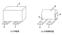
図8に、例えば特許文献1に開示されているスナバコンデンサの外観と内部構成例を示す。
先の図7に示すように、IGBTモジュール上のP端子とN端子間に設置され、P側引出し端子1とN側引出し端子2と樹脂モールドされ、外観が例えば図8(a)のように示されるスナバコンデンサモジュール3の内部は、図8(b)のようにP側導体板4と、N側導体板5とコンデンサ自身となるフィルムエレメント6とから構成される(フィルムコンデンサには極性はないが、ここではIGBT側の極性と合わせて記載した)。
FIG. 8 shows an external appearance and an internal configuration example of a snubber capacitor disclosed in
As shown in the previous FIG. 7, it is installed between the P terminal and the N terminal on the IGBT module, resin-molded with the P
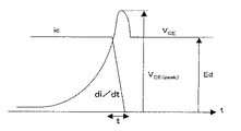
図9に、IGBTがターンオフする際のコレクタ−エミッタ間電圧VCEとコレクタ電流icの波形を示す。
図示の期間tにおいて、コレクタ電流icのdi/dtにより、高いサージ電圧が発生する。このサージ電圧VCE(PEAK)は、次の(1)式により概略計算できる。
VCE(PEAK)=Ed+L1・di/dt+L2・di/dt …(1)
Ed:直流電圧
L1:スナバコンデンサの内部配線などのインダクタンス値
L2:IGBTモジュール内部の配線インダクタンス値(図示なし)
di/dt:IGBTターンオフ時の電流変化率
上記(1)式から、スナバコンデンサの内部インダクタンス値が大きいとVCE(PEAK)が高くなり、そのため耐圧の高いIGBTが必要となる。
FIG. 9 shows waveforms of the collector-emitter voltage V CE and the collector current ic when the IGBT is turned off.
In the illustrated period t, a high surge voltage is generated due to di / dt of the collector current ic . This surge voltage V CE (PEAK) can be roughly calculated by the following equation (1).
V CE (PEAK) = Ed + L1 · di / dt + L2 · di / dt (1)
Ed: DC voltage
L1: Inductance value such as internal wiring of snubber capacitor
L2: Wiring inductance value inside the IGBT module (not shown)
di / dt: Current change rate at IGBT turn-off From the above equation (1), if the internal inductance value of the snubber capacitor is large, V CE (PEAK) becomes high, so that an IGBT with a high withstand voltage is required.
図10にスナバコンデンサの内部に基く等価回路を示す。上記(1)式のL1はP,Nの引出し端子,各導体板およびフィルムエレメント(L1p,L1n,L1pp,L1nn,L1e)よりなるが、配線長からL1eが最も支配的となる。
L1p:P側引出し端子部インダクタンス,L1n:N側引出し端子部インダクタンス
L1pp:P側導体板インダクタンス
L1nn:N側導体板インダクタンス
L1e:フィルムエレメントのインダクタンス
FIG. 10 shows an equivalent circuit based on the inside of the snubber capacitor. L1 in the above formula (1) is composed of P and N lead terminals, conductor plates and film elements (L1p, L1n, L1pp, L1nn, L1e), and L1e is the most dominant from the wiring length.
L1p: P-side lead terminal inductance, L1n: N-side lead terminal inductance L1pp: P-side conductor plate inductance L1nn: N-side conductor plate inductance L1e: Film element inductance
また、別の問題として、IGBTがスイッチングする際、スナバコンデンサ自身の容量と配線インダクタンス18(図5参照)との共振現象(通常数100kHz)や、スナバコンデンサとIGBTモジュール内部の浮遊容量と、その間の配線インダクタンスによって発生する共振現象(通常数10MHz)により、スナバコンデンサ自身がノイズ源となり、周辺回路が誤動作するという問題も生じる。
したがって、この発明の課題は、スイッチ素子によるスイッチング時のサージ電圧の低減、自身がノイズ源となることによる周辺回路誤動作の低減を図ることが可能なコンデンサとその設置方法を提供することにある。
As another problem, when the IGBT switches, the resonance phenomenon (usually several hundred kHz) between the capacitance of the snubber capacitor itself and the wiring inductance 18 (see FIG. 5), the stray capacitance inside the snubber capacitor and the IGBT module, Due to the resonance phenomenon (usually several tens of MHz) caused by the wiring inductance, the snubber capacitor itself becomes a noise source, causing a problem that the peripheral circuit malfunctions.
Accordingly, an object of the present invention is to provide a capacitor capable of reducing a surge voltage at the time of switching by a switch element and reducing malfunction of a peripheral circuit due to itself being a noise source, and an installation method thereof.
このような課題を解決するため、請求項1の発明では、正側電位用端子と負側電位用端子の引き出し端子と、容量成分となるエレメントを支持するそれぞれの導体板とが、前記正側電位用端子と負側電位用端子とを挟む中心線に対し反対側に位置するように、内部または外部に電位極性反転用導体を設けることを特徴とする。
In order to solve such a problem, in the invention of
上記請求項1に記載のコンデンサと従来タイプのコンデンサとを、隣り合わせにして電子機器またはプリント基板上に設置することができる(請求項2の発明)。
また、請求項1に記載のコンデンサと従来タイプのコンデンサとを、1つのモジュール内に収納することができる(請求項3の発明)。
The capacitor according to
Further, the capacitor according to
この発明によれば、特に従来タイプのコンデンサと隣り合わせで用いることで、両コンデンサから発生する漏洩磁界を低減させ、スイッチ素子によるスイッチング時のサージ電圧の低減、自身がノイズ源となることによる周辺回路誤動作の低減を図れるようにする。その結果、スイッチ素子の電圧定格の低減化によるコストダウンや、周辺回路を誤動作させない高信頼の装置を提供することができる。 According to the present invention, particularly when used adjacent to a conventional type capacitor, the leakage magnetic field generated from both capacitors is reduced, the surge voltage at the time of switching by the switch element is reduced, and the peripheral circuit by itself becoming a noise source Reduce malfunctions. As a result, the cost can be reduced by reducing the voltage rating of the switch element, and a highly reliable device that does not malfunction the peripheral circuit can be provided.
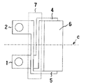
図1はこの発明の第1の実施の形態を示す構成図である。
これは、P側引出し端子1とN側引出し端子2に対し、P側の導体板5とN側の導体板4が、中心線cに対して反対側に位置するように、導体7を追加して構成される。フィルムエレメント6に着目した場合、図1のものと従来タイプのコンデンサとでは、流れる電流が互いに逆になる。
FIG. 1 is a block diagram showing a first embodiment of the present invention.
The
図2は図1の変形例を示す構成図である。
図2(a)は図1に示すものに対し、導体7をコンデンサモジュール3内(コンデンサチップ内部)に収めた例であり、図2(b)は導体7をコンデンサモジュール3内に収めず、外付け(コンデンサチップ外部)とした例である。なお、図1では導体7を端子1や端子2と同一導体を想定しているが、別の導体をねじ留めや半田付けで接続するようにしても良い。
FIG. 2 is a block diagram showing a modification of FIG.
FIG. 2A is an example in which the
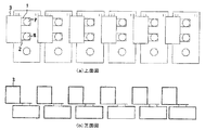
図3はこの発明の第2の実施の形態を説明するための説明図である。
これは、例えば3相出力インバータで、IGBTモジュール20aと20b,21aと21b,22aと22bを2並列接続した例である。つまり、従来タイプのコンデンサ91,92,93をIGBTモジュール20b,21b,22b上にそれぞれ配置するとともに、この発明によるコンデンサ95,96,97をIGBTモジュール20a,21a,22a上にそれぞれ配置して構成する。これにより、隣り合うコンデンサのフィルムエレメント内に流れる電流の向きは、図の矢印で示すように互いに反対方向となる。
FIG. 3 is an explanatory diagram for explaining a second embodiment of the present invention.
This is an example in which two
図4にこの発明の第3の実施の形態を示す。
図3では、コンデンサ91と95、コンデンサ92と96およびコンデンサ93と97はそれぞれ別のコンデンサであるが、ここでは同一のモジュール8内に収めて構成される。こうすることで、図3のものより一層低インダクタンス化や低ノイズ化が図られ、小型化,低コスト化も可能となる。
FIG. 4 shows a third embodiment of the present invention.
In FIG. 3,
以上では、電力変換装置に用いるスナバコンデンサを例に説明したが、この発明はプリント板上に設置されるフィルムコンデンサや積層チップコンデンサ等にも、同様にして適用することができる。例えば、バイパスコンデンサ用のチップコンデンサにおいて、隣り合って設置する場合などに用いることができる。 In the above description, the snubber capacitor used in the power converter is described as an example. However, the present invention can be similarly applied to a film capacitor, a multilayer chip capacitor, and the like installed on a printed board. For example, in a chip capacitor for a bypass capacitor, it can be used when installed adjacent to each other.
1…P側引出し端子、2…N側引出し端子、3…スナバコンデンサモジュール、4…P側導体板、5…N側導体板、6…フィルムエレメント、7…導体、8…モジュール、91,92,93,95,96,97…コンデンサ、20a,20b,21a,21b,22a,22b…IGBTモジュール。
DESCRIPTION OF
Claims (3)
A capacitor comprising the capacitor according to claim 1 and a conventional type capacitor accommodated in one module.
Priority Applications (1)
| Application Number | Priority Date | Filing Date | Title |
|---|---|---|---|
| JP2004236948A JP4487682B2 (en) | 2004-08-17 | 2004-08-17 | Capacitor and installation method |
Applications Claiming Priority (1)
| Application Number | Priority Date | Filing Date | Title |
|---|---|---|---|
| JP2004236948A JP4487682B2 (en) | 2004-08-17 | 2004-08-17 | Capacitor and installation method |
Publications (2)
| Publication Number | Publication Date |
|---|---|
| JP2006060876A JP2006060876A (en) | 2006-03-02 |
| JP4487682B2 true JP4487682B2 (en) | 2010-06-23 |
Family
ID=36107902
Family Applications (1)
| Application Number | Title | Priority Date | Filing Date |
|---|---|---|---|
| JP2004236948A Expired - Fee Related JP4487682B2 (en) | 2004-08-17 | 2004-08-17 | Capacitor and installation method |
Country Status (1)
| Country | Link |
|---|---|
| JP (1) | JP4487682B2 (en) |
Cited By (1)
| Publication number | Priority date | Publication date | Assignee | Title |
|---|---|---|---|---|
| CN110168903A (en) * | 2016-12-13 | 2019-08-23 | 日立汽车系统株式会社 | Busbar construction and the power-converting device using it |
Families Citing this family (3)
| Publication number | Priority date | Publication date | Assignee | Title |
|---|---|---|---|---|
| JP6102668B2 (en) * | 2013-10-03 | 2017-03-29 | 三菱電機株式会社 | Power converter |
| WO2018043002A1 (en) * | 2016-09-02 | 2018-03-08 | 三菱電機株式会社 | Bus bar structure and power conversion device using same |
| JP2020088888A (en) | 2018-11-15 | 2020-06-04 | 株式会社日立製作所 | Voltage filter and power conversion device |
Family Cites Families (5)
| Publication number | Priority date | Publication date | Assignee | Title |
|---|---|---|---|---|
| JPS6112665Y2 (en) * | 1981-01-09 | 1986-04-19 | ||
| JP2001251845A (en) * | 2000-03-06 | 2001-09-14 | Matsushita Electric Ind Co Ltd | Snubber capacitor |
| JP4476465B2 (en) * | 2000-10-04 | 2010-06-09 | 三菱電機株式会社 | Power converter |
| JP2003318066A (en) * | 2002-04-25 | 2003-11-07 | Taiyo Yuden Co Ltd | Capacitor module |
| JP3780975B2 (en) * | 2002-05-22 | 2006-05-31 | 松下電器産業株式会社 | Capacitor manufacturing method and capacitor |
-
2004
- 2004-08-17 JP JP2004236948A patent/JP4487682B2/en not_active Expired - Fee Related
Cited By (2)
| Publication number | Priority date | Publication date | Assignee | Title |
|---|---|---|---|---|
| CN110168903A (en) * | 2016-12-13 | 2019-08-23 | 日立汽车系统株式会社 | Busbar construction and the power-converting device using it |
| CN110168903B (en) * | 2016-12-13 | 2020-11-13 | 日立汽车系统株式会社 | Busbar structure and power conversion device using same |
Also Published As
| Publication number | Publication date |
|---|---|
| JP2006060876A (en) | 2006-03-02 |
Similar Documents
| Publication | Publication Date | Title |
|---|---|---|
| EP2264894B1 (en) | Power module with additional transient current path and power module system | |
| JP6041862B2 (en) | Power converter | |
| JP5369922B2 (en) | 3-level power converter | |
| US8901602B2 (en) | Power semiconductor device and power conversion system using the device | |
| US20180205309A1 (en) | High Power Density Inverter (I) | |
| JP2009022062A (en) | Wiring structure of 3-level power conversion circuit | |
| JP2006197735A (en) | Inverter | |
| JP2011254672A (en) | Power semiconductor module and power conversion device using the same | |
| JP2005065412A (en) | Stack structure in power converter | |
| JP5571013B2 (en) | Semiconductor switch and power conversion device | |
| JP2007181351A (en) | Inverter module of power converter | |
| JP4487682B2 (en) | Capacitor and installation method | |
| JP2010199473A (en) | Power conversion unit | |
| US10165701B2 (en) | Electric power conversion device for providing a stabilized potential to a cooler | |
| CN111527684A (en) | Power module with built-in driving circuit | |
| JP6289577B2 (en) | Power converter | |
| JP2020005411A (en) | Electric power conversion device | |
| JP5307370B2 (en) | Power conversion circuit | |
| JP5516623B2 (en) | Power converter | |
| JPH01209951A (en) | Power conversion device | |
| JP2015089185A (en) | Three-level power conversion device | |
| JP2005197433A (en) | Power semiconductor module | |
| JP6344054B2 (en) | Series connection capacitor placement and wiring structure | |
| CN115514188A (en) | Power conversion device | |
| JP2008236855A (en) | Power conversion device |
Legal Events
| Date | Code | Title | Description |
|---|---|---|---|
| A621 | Written request for application examination |
Free format text: JAPANESE INTERMEDIATE CODE: A621 Effective date: 20070614 |
|
| TRDD | Decision of grant or rejection written | ||
| A01 | Written decision to grant a patent or to grant a registration (utility model) |
Free format text: JAPANESE INTERMEDIATE CODE: A01 Effective date: 20100309 |
|
| A01 | Written decision to grant a patent or to grant a registration (utility model) |
Free format text: JAPANESE INTERMEDIATE CODE: A01 |
|
| A61 | First payment of annual fees (during grant procedure) |
Free format text: JAPANESE INTERMEDIATE CODE: A61 Effective date: 20100322 |
|
| FPAY | Renewal fee payment (prs date is renewal date of database) |
Free format text: PAYMENT UNTIL: 20130409 Year of fee payment: 3 |
|
| R150 | Certificate of patent (=grant) or registration of utility model |
Free format text: JAPANESE INTERMEDIATE CODE: R150 |
|
| FPAY | Renewal fee payment (prs date is renewal date of database) |
Free format text: PAYMENT UNTIL: 20130409 Year of fee payment: 3 |
|
| S533 | Written request for registration of change of name |
Free format text: JAPANESE INTERMEDIATE CODE: R313533 |
|
| FPAY | Renewal fee payment (prs date is renewal date of database) |
Free format text: PAYMENT UNTIL: 20130409 Year of fee payment: 3 |
|
| R350 | Written notification of registration of transfer |
Free format text: JAPANESE INTERMEDIATE CODE: R350 |
|
| LAPS | Cancellation because of no payment of annual fees |