JP4085976B2 - Inverter control device and control method - Google Patents
Inverter control device and control method Download PDFInfo
- Publication number
- JP4085976B2 JP4085976B2 JP2003431112A JP2003431112A JP4085976B2 JP 4085976 B2 JP4085976 B2 JP 4085976B2 JP 2003431112 A JP2003431112 A JP 2003431112A JP 2003431112 A JP2003431112 A JP 2003431112A JP 4085976 B2 JP4085976 B2 JP 4085976B2
- Authority
- JP
- Japan
- Prior art keywords
- frequency
- carrier
- inverter
- carrier wave
- value
- Prior art date
- Legal status (The legal status is an assumption and is not a legal conclusion. Google has not performed a legal analysis and makes no representation as to the accuracy of the status listed.)
- Expired - Fee Related
Links
Images


Classifications
-
- H—ELECTRICITY
- H02—GENERATION; CONVERSION OR DISTRIBUTION OF ELECTRIC POWER
- H02M—APPARATUS FOR CONVERSION BETWEEN AC AND AC, BETWEEN AC AND DC, OR BETWEEN DC AND DC, AND FOR USE WITH MAINS OR SIMILAR POWER SUPPLY SYSTEMS; CONVERSION OF DC OR AC INPUT POWER INTO SURGE OUTPUT POWER; CONTROL OR REGULATION THEREOF
- H02M7/00—Conversion of ac power input into dc power output; Conversion of dc power input into ac power output
- H02M7/42—Conversion of dc power input into ac power output without possibility of reversal
- H02M7/44—Conversion of dc power input into ac power output without possibility of reversal by static converters
- H02M7/48—Conversion of dc power input into ac power output without possibility of reversal by static converters using discharge tubes with control electrode or semiconductor devices with control electrode
- H02M7/53—Conversion of dc power input into ac power output without possibility of reversal by static converters using discharge tubes with control electrode or semiconductor devices with control electrode using devices of a triode or transistor type requiring continuous application of a control signal
- H02M7/537—Conversion of dc power input into ac power output without possibility of reversal by static converters using discharge tubes with control electrode or semiconductor devices with control electrode using devices of a triode or transistor type requiring continuous application of a control signal using semiconductor devices only, e.g. single switched pulse inverters
- H02M7/5387—Conversion of dc power input into ac power output without possibility of reversal by static converters using discharge tubes with control electrode or semiconductor devices with control electrode using devices of a triode or transistor type requiring continuous application of a control signal using semiconductor devices only, e.g. single switched pulse inverters in a bridge configuration
- H02M7/53871—Conversion of dc power input into ac power output without possibility of reversal by static converters using discharge tubes with control electrode or semiconductor devices with control electrode using devices of a triode or transistor type requiring continuous application of a control signal using semiconductor devices only, e.g. single switched pulse inverters in a bridge configuration with automatic control of output voltage or current
- H02M7/53875—Conversion of dc power input into ac power output without possibility of reversal by static converters using discharge tubes with control electrode or semiconductor devices with control electrode using devices of a triode or transistor type requiring continuous application of a control signal using semiconductor devices only, e.g. single switched pulse inverters in a bridge configuration with automatic control of output voltage or current with analogue control of three-phase output
-
- H—ELECTRICITY
- H02—GENERATION; CONVERSION OR DISTRIBUTION OF ELECTRIC POWER
- H02M—APPARATUS FOR CONVERSION BETWEEN AC AND AC, BETWEEN AC AND DC, OR BETWEEN DC AND DC, AND FOR USE WITH MAINS OR SIMILAR POWER SUPPLY SYSTEMS; CONVERSION OF DC OR AC INPUT POWER INTO SURGE OUTPUT POWER; CONTROL OR REGULATION THEREOF
- H02M7/00—Conversion of ac power input into dc power output; Conversion of dc power input into ac power output
- H02M7/42—Conversion of dc power input into ac power output without possibility of reversal
- H02M7/44—Conversion of dc power input into ac power output without possibility of reversal by static converters
- H02M7/48—Conversion of dc power input into ac power output without possibility of reversal by static converters using discharge tubes with control electrode or semiconductor devices with control electrode
- H02M7/53—Conversion of dc power input into ac power output without possibility of reversal by static converters using discharge tubes with control electrode or semiconductor devices with control electrode using devices of a triode or transistor type requiring continuous application of a control signal
- H02M7/537—Conversion of dc power input into ac power output without possibility of reversal by static converters using discharge tubes with control electrode or semiconductor devices with control electrode using devices of a triode or transistor type requiring continuous application of a control signal using semiconductor devices only, e.g. single switched pulse inverters
- H02M7/539—Conversion of dc power input into ac power output without possibility of reversal by static converters using discharge tubes with control electrode or semiconductor devices with control electrode using devices of a triode or transistor type requiring continuous application of a control signal using semiconductor devices only, e.g. single switched pulse inverters with automatic control of output wave form or frequency
- H02M7/5395—Conversion of dc power input into ac power output without possibility of reversal by static converters using discharge tubes with control electrode or semiconductor devices with control electrode using devices of a triode or transistor type requiring continuous application of a control signal using semiconductor devices only, e.g. single switched pulse inverters with automatic control of output wave form or frequency by pulse-width modulation
-
- H—ELECTRICITY
- H02—GENERATION; CONVERSION OR DISTRIBUTION OF ELECTRIC POWER
- H02P—CONTROL OR REGULATION OF ELECTRIC MOTORS, ELECTRIC GENERATORS OR DYNAMO-ELECTRIC CONVERTERS; CONTROLLING TRANSFORMERS, REACTORS OR CHOKE COILS
- H02P21/00—Arrangements or methods for the control of electric machines by vector control, e.g. by control of field orientation
- H02P21/05—Arrangements or methods for the control of electric machines by vector control, e.g. by control of field orientation specially adapted for damping motor oscillations, e.g. for reducing hunting
-
- H—ELECTRICITY
- H02—GENERATION; CONVERSION OR DISTRIBUTION OF ELECTRIC POWER
- H02M—APPARATUS FOR CONVERSION BETWEEN AC AND AC, BETWEEN AC AND DC, OR BETWEEN DC AND DC, AND FOR USE WITH MAINS OR SIMILAR POWER SUPPLY SYSTEMS; CONVERSION OF DC OR AC INPUT POWER INTO SURGE OUTPUT POWER; CONTROL OR REGULATION THEREOF
- H02M1/00—Details of apparatus for conversion
- H02M1/44—Circuits or arrangements for compensating for electromagnetic interference in converters or inverters
Description
本発明は、直流電源の出力をPWM(Pulse Wide Modulation)変調することによりモータに供給する正弦波状の交流電圧を出力するインバータの制御装置及び制御方法に関し、より詳しくは、モータ効率を悪化させることなく、搬送波に起因する不具合の発生を防止する技術に係わる。 The present invention relates to a control device and control method for an inverter that outputs a sinusoidal AC voltage supplied to a motor by PWM (Pulse Wide Modulation) modulation of the output of the DC power supply, and more specifically, to deteriorate motor efficiency. In particular, the present invention relates to a technique for preventing the occurrence of defects caused by carrier waves.
従来より、3相ブラシレス直流モータ(以下、モータと略記)のU相,V相,W相の各相の電流値を検出し、正弦波状の電流指令値に従うように検出値をPID(比例・積分・微分)制御してPID制御値を生成し、PID制御値を変調するためにPID制御値と三角波状搬送波(以下、搬送波と略記)の大小関係に応じてインバータを構成するスイッチング素子のオン/オフを切り換える制御装置が知られている。そして、このような制御装置によれば、モータのU相,V相,W相の各相に正弦波状の電流が流れるようにフィードバック制御を行うことが可能となる。 Conventionally, the current value of each of the U-phase, V-phase, and W-phase of a three-phase brushless DC motor (hereinafter abbreviated as “motor”) is detected, and the detected value is set to PID (proportional / Integral / differential) control is performed to generate a PID control value, and in order to modulate the PID control value, the switching elements constituting the inverter are turned on according to the magnitude relationship between the PID control value and the triangular wave carrier wave (hereinafter abbreviated as carrier wave) Control devices for switching between on and off are known. According to such a control device, it is possible to perform feedback control so that a sinusoidal current flows in each phase of the U phase, V phase, and W phase of the motor.
ところで、上記インバータは、一般に、三角波比較型正弦波PWMインバータと呼ばれているが、この三角波比較型正弦波PWMインバータは、スイッチング動作に伴い、機械的/電気的振動,雑音,騒音,EMI(ElectroMagnetic Interference)等、搬送波の周波数に起因する不具合を発生することが知られている。このため、従来までの制御装置は、搬送波の周波数に起因する機械的/電気的振動を低減するために、搬送波の周波数をランダムに切り換え、搬送波のスペクトラムを拡散させることにより、スペクトラムのピーク値を低く抑えている(例えば、特許文献1を参照)。
しかしながら、一般に、PID制御を行う際の積分定数は搬送波の周波数に依存しているために、上記従来までの制御装置のように搬送波の周波数をランダムに切り換えた場合には、積分定数の計算が複雑になり、PID制御の遅れ時間が増大する。さらに、インバータを制御する際は、通常、各相電流をサンプリングするために発生する遅れ時間,PID制御の遅れ時間,制御周期による遅れ時間等の制御遅れ時間を補償するために、制御遅れ時間を予測し、フィードフォワードによる遅れ補償が行われるが、上記従来までの制御装置のように搬送波の周波数をランダムに切り換えた場合には、制御遅れを予測することが困難になるので、制御遅れを補償することができない。これらの理由から、従来までの制御装置によれば、電流を十分な精度で正弦波状に制御することができず、モータ効率が悪化することがある。 However, in general, since the integration constant when performing PID control depends on the frequency of the carrier wave, when the carrier frequency is switched at random as in the conventional control device, the calculation of the integration constant is not possible. It becomes complicated and the delay time of PID control increases. Further, when controlling the inverter, the control delay time is usually set to compensate for the control delay time such as the delay time generated for sampling each phase current, the delay time of the PID control, and the delay time due to the control cycle. Prediction and feedforward delay compensation is performed, but when the carrier frequency is switched randomly as in the conventional control device, it is difficult to predict the control delay, so the control delay is compensated. Can not do it. For these reasons, according to the conventional control device, the current cannot be controlled in a sine wave shape with sufficient accuracy, and the motor efficiency may deteriorate.
本発明は、上記課題を解決するためになされたものであり、モータ効率を悪化させることなく、搬送波に起因する不具合の発生を防止可能なインバータの制御装置及び制御方法を提供することにある。 The present invention has been made to solve the above-described problems, and it is an object of the present invention to provide an inverter control device and control method capable of preventing the occurrence of problems caused by a carrier wave without deteriorating motor efficiency.
上記課題を解決するために、精力的な研究を重ねてきた結果、発明者は、搬送波の周波数が所定の波形状で変化するように搬送波の周波数を変調することにより、モータ効率を悪化させることなく、搬送波に起因する不具合の発生を防止できることを知見した。 As a result of intensive research to solve the above problems, the inventors have deteriorated motor efficiency by modulating the frequency of the carrier so that the frequency of the carrier changes with a predetermined wave shape. It has been found that it is possible to prevent the occurrence of defects due to carrier waves.
上記知見に基づいた本発明に係るインバータの制御装置の一態様は、スイッチング素子のオン/オフを切り換えることにより負荷に接続する直流電源の正極/負極を切り換え、負荷に対して正弦波状の交流電流を供給するインバータの制御装置であって、正弦波状の電流指令値を生成する電流指令生成部と、三角状の搬送波を生成する三角状搬送波生成部と、電流指令値に従うようにインバータの出力値をPID制御するPID制御部と、PID制御部の出力値と搬送波の大小関係に従ってスイッチング素子のオン/オフ動作を制御する比較器と、搬送波の周波数が所定の波形状で変化するように周波数を変調する搬送波周波数生成部とを備える。 One aspect of the inverter control device according to the present invention based on the above knowledge is to switch a positive / negative polarity of a DC power source connected to a load by switching on / off of a switching element, and a sinusoidal AC current with respect to the load. A current command generator for generating a sinusoidal current command value, a triangular carrier wave generator for generating a triangular carrier wave, and an inverter output value in accordance with the current command value A PID control unit that performs PID control, a comparator that controls the on / off operation of the switching element according to the magnitude relationship between the output value of the PID control unit and the carrier wave, and the frequency so that the frequency of the carrier wave changes in a predetermined waveform A carrier frequency generation unit for modulation.
また、上記知見に基づいた本発明に係るインバータの制御方法の一態様は、スイッチング素子のオン/オフを切り換えることにより負荷に接続する直流電源の正極/負極を切り換え、負荷に対して正弦波状の交流電流を供給するインバータの制御方法であって、正弦波状の電流指令値を生成するステップと、三角状の搬送波を生成するステップと、電流指令値に従うようにインバータの出力値をPID制御するステップと、PID制御後のインバータの出力値と搬送波の大小関係に従ってスイッチング素子のオン/オフ動作を制御するステップと、搬送波の周波数が所定の波形状で変化するように周波数を変調するステップとを有する。 Also, one aspect of the inverter control method according to the present invention based on the above knowledge is to switch the positive / negative polarity of the DC power supply connected to the load by switching on / off of the switching element, A method for controlling an inverter for supplying an alternating current, the step of generating a sinusoidal current command value, the step of generating a triangular carrier wave, and the step of PID controlling the output value of the inverter so as to follow the current command value And a step of controlling the on / off operation of the switching element according to the magnitude relationship between the output value of the inverter after PID control and the carrier wave, and a step of modulating the frequency so that the frequency of the carrier wave changes in a predetermined waveform. .
本発明に係るインバータの制御装置及び制御方法によれば、搬送波の周波数が所定の波形状で変化するので、モータ効率を悪化させることなく、搬送波の周波数に起因する不具合の発生を防止することができる。 According to the control device and the control method for an inverter according to the present invention, since the frequency of the carrier wave changes with a predetermined waveform, it is possible to prevent the occurrence of a malfunction due to the frequency of the carrier wave without deteriorating the motor efficiency. it can.
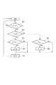
本発明は、図1に示すような、直流電源の出力をPWM変調することにより正弦波状の交流電流をモータに供給するインバータを備えるインバータシステムに適用することができる。以下、図面を参照して、本発明の第1,第2,第3の実施形態となるインバータシステムの構成と動作について説明する。 The present invention can be applied to an inverter system including an inverter that supplies a sinusoidal AC current to a motor by PWM-modulating the output of a DC power source as shown in FIG. Hereinafter, the configuration and operation of the inverter system according to the first, second, and third embodiments of the present invention will be described with reference to the drawings.
始めに、図1〜図8を参照して、本発明の第1の実施形態となるインバータシステムの構成と動作について説明する。 First, the configuration and operation of the inverter system according to the first embodiment of the present invention will be described with reference to FIGS.
[インバータシステムの構成]
本発明の第1の実施形態となるインバータシステム1は、図1に示すように、PWMインバータ2、3相ブラシレス直流モータ(以下、モータと略記)3、電流センサ4a,4b,4c、電流指令生成部5、PID制御部6a,6b,6c、三角波状搬送波生成部7、比較器8a,8b,8c、及び搬送波周波数生成部9を主な構成要素として備える。
[Inverter system configuration]
As shown in FIG. 1, an
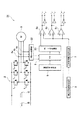
上記PWMインバータ2は、比較器8a,8b,8cの制御に従って電池B及びコンデンサCから成る直流電源の正極又は負極を選択し、選択した電極をモータ3のU相,V相,W相の各電極に接続する6個のスイッチング素子Tu+,Tu−,Tv+,Tv−,Tw+,Tw−を備え、これらのスイッチング素子はIGBT(Insulated Gate Bipolar Transistor)等の半導体素子により構成されている。
The
上記電流センサ4a,4b,4cはそれぞれ、PWMインバータ2からモータ3に供給されるU相,V相,W相の電流値を検出し、上記電流指令生成部5は、電流センサ4a,4b,4cの検出値が正弦波状の交流電流に変換されるように、正弦波状の電流指令値を生成する。上記PID制御部6a,6b,6cは、電流センサ4a,4b,4cの検出値が電流指令生成部5が生成した電流指令値に従うように、電流センサ4a,4b,4cの検出値をPID制御する。上記三角波状搬送波生成部7は三角波状搬送波を生成する。
The
上記比較器8a,8b,8cは、PID制御部6a,6b,6cの出力値と三角波状搬送波の大小関係を比較し、その大小関係に応じてPWMインバータ2のスイッチング素子Tu+,Tu−,Tv+,Tv−,Tw+,Tw−のオン/オフを制御する信号をPWMインバータ2に入力する。U相のスイッチング素子Tu+,Tu−の制御を例として比較器8aの動作を具体的に説明すれば、比較器8aは、PID制御部6aの出力値が三角状搬送波よりも大きい場合、Tu+,Tu−をそれぞれオン状態及びオフ状態に制御することにより正の電圧をモータのU相に印加し、逆にPID制御部の出力値6aが三角状搬送波よりも小さい場合には、Tu+,Tu−をそれぞれオフ状態及びオン状態に制御することにより、負の電圧をモータのU相に印加する。
The
上記搬送波周波数生成部9は、三角波状搬送波生成部7から入力される三角状搬送波の山(最大値)又は谷(最小値)のタイミングに合わせて、三角状搬送波の周波数fを変化させる(詳しくは後述する)。
The carrier
[周波数制御処理]
このような構成を有するインバータシステムでは、搬送波周波数生成部9が、以下に示す周波数制御処理を実行することにより、モータ効率を悪化させることなく、搬送波に起因する不具合の発生を防止する。以下、図2に示すフローチャートを参照して、この周波数制御処理を実行する際の搬送波周波数生成部9の動作について詳しく説明する。
[Frequency control processing]
In the inverter system having such a configuration, the carrier
図2に示すフローチャートは、三角状搬送波生成部7から搬送波周波数生成部9に三角状搬送波(以下、搬送波と略記)が入力されることで開始となり、この周波数制御処理はステップS1の処理に進む。
The flowchart shown in FIG. 2 starts when a triangular carrier wave (hereinafter abbreviated as a carrier wave) is input from the triangular
ステップS1の処理では、搬送波周波数生成部9が、三角状搬送波生成部7から入力された搬送波が最大値若しくは最小値(ピーク)であるか否かを判別する。そして、搬送波が最大値若しくは最小値であると判別するのに応じて、搬送波周波数生成部9は、この周波数制御処理をステップS2の処理に進める。
In the process of step S1, the carrier
ステップS2の処理では、搬送波周波数生成部9が、搬送波の周波数fの変化値Δが正,負のどちらであるかを判別する。そして、変化値Δが負である場合、搬送波周波数生成部9は、この周波数制御処理をステップS5の処理に進める。一方、変化値Δが正である場合には、搬送波周波数生成部9は、この周波数制御処理をステップS3の処理に進める。
In the process of step S2, the carrier wave
ステップS3の処理では、搬送波周波数生成部9が、周波数fが上限値fmaxに達しているか否かを判別する。そして、判別の結果、周波数fが上限値fmaxに達していない場合、搬送波周波数生成部9は、変化値Δを変化させないように、この周波数制御処理をステップS7の処理に進める。一方、周波数fが上限値fmaxに達している場合には、搬送周波数生成部9は、この周波数制御処理をステップS4の処理に進める。
In the process of step S3, the
ステップS4の処理では、搬送波周波数生成部9が、周波数fを上限値fmaxから減少させるように、周波数fの変化値Δを変転させる。これにより、このステップS4の処理は完了し、この周波数制御処理はステップS4の処理からステップS7の処理に進む。
In the process of step S4, the carrier
ステップS5の処理では、搬送波周波数生成部9が、周波数fが下限値fminに達しているか判別する。そして、判別の結果、周波数fが下限値fminに達していない場合、搬送波周波数生成部9は、変化値Δを変化させないように、この周波数制御処理をステップS7の処理に進める。一方、周波数fが下限値fminに達している場合には、搬送波周波数生成部9は、この周波数制御処理をステップS6の処理に進める。
In the process of step S5, the
ステップS6の処理では、搬送波周波数生成部9が、周波数fを下限値fminから増加させるように、周波数fの変化値Δを変転させる。これにより、このステップS6の処理は完了し、この周波数制御処理はステップ6の処理からステップS7の処理に進む。
In the process of step S6, the carrier
ステップS7の処理では、搬送波周波数生成部9が、上記処理により決定された変化値Δを現在の周波数fに加算した値を次周期の搬送波周波数fとして三角波状搬送波生成部7に入力する。これにより、このステップS7の処理は完了し、この周波数制御処理はステップS7の処理からステップS1の処理に戻る。そして、この一連の周波数制御処理によれば、図3に示すように、ある区間では搬送波周波数fを単調に減少、ある区間では単調に増加させることにより、搬送波の周波数を三角状に変調し、図4の実線に示すような三角状搬送波を生成することができる。なお、図3,図4はそれぞれ、搬送波の周波数をランダム及び三角状に変調した時の搬送波周波数の時間的変化、及び搬送波周波数が一定(点線)及び三角状に変調されている(実線)時の搬送波の時間的変化を示す。また、この実施形態では、図3に示すように、搬送波の周波数を直線状に変化させたが、周波数をランダムに変化させた場合等のように、搬送波の周波数fの変化量が大きくならない限り、例えば曲線状に変化させる等、周波数をどのような形状で変化させてもよい。
In step S7, the carrier
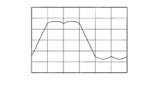
ここで、図5を参照して、搬送波周波数fを固定,ランダム,及び三角状に変調にした時のモータ相電流の変化について説明する。なお、図5(a),(b),(c)はそれぞれ、搬送波周波数fを固定,ランダム,及び三角状に変調にした時のモータ相電流のスペクトラムのシミュレーション結果を示す。 Here, with reference to FIG. 5, the change of the motor phase current when the carrier frequency f is modulated in a fixed, random, and triangular shape will be described. 5A, 5B, and 5C show simulation results of the spectrum of the motor phase current when the carrier frequency f is modulated in a fixed, random, and triangular shape, respectively.
図5から明らかなように、モータ相電流の高調波のピークは、固定,ランダム変調,三角状変調の順に低くなることがわかる。具体的には、20[kHz]では、搬送波周波数fを固定した場合のピーク値は11[dBA]であるのに対し、ランダム変調した場合は5[dBA]、三角状変調した場合には0[dBA]まで低減している。また、30[kHz]では、搬送波周波数を固定した場合のピーク値は−1[dBA]であるのに対し、ランダム変調した場合には−4[dBA]、三角状変調した場合には−15[dBA]まで低減している。 As is clear from FIG. 5, the harmonic peak of the motor phase current decreases in the order of fixed, random modulation, and triangular modulation. Specifically, at 20 [kHz], the peak value when the carrier frequency f is fixed is 11 [dBA], whereas when the random modulation is performed, the peak value is 5 [dBA], and when the triangular modulation is performed, the peak value is 0. Reduced to [dBA]. Further, at 30 [kHz], the peak value when the carrier frequency is fixed is -1 [dBA], whereas when random modulation is performed, -4 [dBA] is obtained, and when triangular modulation is performed, -15. Reduced to [dBA].
従って、搬送波の周波数を三角状に変調した場合には、従来までのように搬送波周波数をランダムに変調する場合と比較して、モータ相電流のスペクトラムのピーク値をより多く低減することができるので、搬送波の周波数に起因する不具合の発生をより効果的に防止することができる。 Therefore, when the carrier frequency is modulated in a triangular shape, the peak value of the spectrum of the motor phase current can be reduced more than in the case where the carrier frequency is randomly modulated as in the prior art. In addition, it is possible to more effectively prevent the occurrence of problems caused by the frequency of the carrier wave.
以上の説明から明らかなように、本発明の第1の実施形態となるインバータシステム1によれば、搬送波周波数生成部9が、搬送波の周波数fを三角状に変調するので、周波数fをランダムに変調した場合と比較して、搬送波の周波数に起因する不具合の発生をより効果的に防止することができる。
As is clear from the above description, according to the
また、本発明の第1の実施形態となるインバータシステム1によれば、搬送波周波数生成部9は、搬送波周波数fを三角状に変調するので、搬送波周波数fを容易に計算,予測することが可能となる。そして、このような構成によれば、周波数fやPID制御の積分定数の計算に要する時間を最小に抑えることができるので、計算時間に起因する制御の遅れ時間を最小に抑え、モータ効率が悪化することを防止できる。
Further, according to the
さらに、本発明の第1の実施形態となるインバータシステム1によれば、搬送波周波数生成部9が、搬送波周波数fを三角状に変調するので、制御遅れ時間を容易に予測することが可能となる。そして、このような構成によれば、フィードフォワードによる遅れ補償を行い、モータ効率が悪化することを防止できる。
Furthermore, according to the
また、本発明の第1の実施形態となるインバータシステム1によれば、搬送波周波数生成部9が、三角状搬送波生成部7から入力された搬送波が最大値若しくは最小値であるか否かを判別し、搬送波が最大値若しくは最小値のピークである場合、搬送波の周波数fの変化値Δを変転させるので、搬送波の周期の途中で制御の周期が変化したために積分定数の再計算を行うことができず、電流制御の精度が悪化することを防止できる。また、搬送波の周期の途中で制御の周期が変化したために、制御遅れ補償を再計算することができず、電流制御の精度が悪化することを防止できる。
Further, according to the
次に、図6を参照して、本発明の第2の実施形態となるインバータシステムの構成と動作について説明する。 Next, the configuration and operation of the inverter system according to the second embodiment of the present invention will be described with reference to FIG.
上記第1の実施形態では、U相,V相,W相各相の正弦波指令値に対してPID制御を行ったが、一般に、マイクロコンピュータ等を利用してPID制御部をデジタル形態で実現する場合には、このような方法はPID制御の精度を悪くすることが知られている。そこで、本発明の第2の実施形態となるインバータシステム21は、図6に示すように、3相→dq変換部22が、電流センサの検出値をdq仮想軸上に変換し、PID制御部6は、dq仮想軸上でPID制御を行う。そして、dq→3相変換部23は、PID制御部6の出力値をU相,V相,W相の3相軸上に逆変換した後に比較器に入力する。
In the first embodiment, the PID control is performed on the sine wave command values of the U phase, the V phase, and the W phase. Generally, the PID control unit is realized in a digital form using a microcomputer or the like. In such a case, such a method is known to deteriorate the accuracy of PID control. Therefore, in the
以上の説明から明らかなように、本発明の第2の実施形態となるインバータシステムによれば、3相→dq変換部22が、電流センサの検出値をdq仮想軸上に変換し、PID制御部6は、dq仮想軸上でPID制御を行う。これにより、dq仮想軸上では電流指令値が直流になるので、PID制御を容易にデジタル形態で実現することができる。
As is apparent from the above description, according to the inverter system according to the second embodiment of the present invention, the three-phase → dq
また、本発明の第2の実施形態となるインバータシステムによれば、PID制御部6,三角状搬送波生成部7,搬送波周波数生成部9,3相→dq変換部22,及びdq→3相変換部23をデジタル形態で構成することが可能になるので、インバータシステムを安価に構成することができる。
Further, according to the inverter system according to the second embodiment of the present invention, the
次に、図7に示すように、本発明の第3の実施形態となるインバータシステムの構成について説明する。 Next, as shown in FIG. 7, the configuration of the inverter system according to the third embodiment of the present invention will be described.
本発明の第3の実施形態となるインバータシステム31は、図7に示すように、dq→3相変換部23に遅れ補償部32が設けられている点が上記第2の実施形態となるインバータシステム21の構成とは異なる。そして、この遅れ補償部32は、搬送波周波数生成部9が生成した搬送波の周波数fに基づいて制御遅れ時間を計算し、計算結果に基づいて電流指令値を補正する。
As shown in FIG. 7, the
以上の説明から明らかなように、本発明の第3の実施形態となるインバータシステム31によれば、遅れ補償部32が、搬送波の周波数fに基づいて制御遅れ時間を計算するので、制御遅れを精度良く補償し、モータ効率が悪化することを防止できる。
As is apparent from the above description, according to the
以上、本発明者によってなされた発明を適用した実施の形態について説明したが、この実施の形態による本発明の開示の一部をなす論述及び図面により本発明は限定されることはない。例えば、上記実施形態では、電流指令生成部5は、正弦波状の電流指令値を生成したが、基本波に3次高調波を加えた波形や図8に示すような正弦波に三角波を加えた波形の電流指令値を生成してもよい。このような波形の電流指令値を用いることにより、電圧の利用効率を向上させることが可能となる。また、上記実施形態では、搬送波の周波数を三角状に変調したが、三角状と近似できる波形であればどのような波形に変調してもよい。具体的には、搬送波の周期を三角状に変調しても、その周波数は、第1次近似では三角状になるので、上述の実施形態と同様の技術的効果を得ることができる。なお、搬送波の周期を三角状に変調する処理は、具体的には図9のフローチャートに示す処理により行うことができる。すなわち、搬送波の周期tを1増数し(ステップS11)、周期tが所定の周期τ以上になるのに応じて(ステップS12)、周期tを1減数する(ステップS13)。そして、減数した周期tが0である場合、周期tの変化値Δが0以上であるか否かを判別し(ステップS15)、減数した周期tが0でない場合には、ステップS13の処理に戻る。ステップS15の処理の結果、周期τの変化値Δが0以上であると判別された場合、周期τが最大値τmaxに達しているか判別し(ステップS16)、周期τが最大値τmaxに達している場合、時刻τの変化値Δを変転させる(ステップS17)。一方、周期τの変化値Δが0以下である場合には、周期τが最小値τminに達してるか否かを判別し(ステップS18)、周期τが最小値τmaxに達している場合、周期τの変化値Δを変転させる(ステップS19)。そして、これらの処理により決定された変化値Δを現在の周期τに加算した後(ステップS20)、この処理を再びステップS11の処理に戻す。このように、上記実施の形態に基づいて当業者等によりなされる他の実施の形態、実施例及び運用技術等は全て本発明の範疇に含まれることは勿論であることを付け加えておく。
As mentioned above, although the embodiment to which the invention made by the present inventor is applied has been described, the present invention is not limited by the description and the drawings that form part of the disclosure of the present invention according to this embodiment. For example, in the above embodiment, the current
1,21,31:インバータシステム
2:PWMインバータ
3:3相ブラシレス直流モータ
4a,4b,4c:電流センサ
5:電流指令生成部
6,6a,6b,6c:PID制御部
7:三角波状搬送波生成部
8a,8b,8c:比較器
9:搬送波周波数生成部
22:3相→dq変換部
23:dq→3相変換部
32:遅れ補償部
1, 21, 31: Inverter system 2: PWM inverter 3: Three-phase
Claims (5)
正弦波状の電流指令値を生成する電流指令生成部と、
三角状の搬送波を生成する三角状搬送波生成部と、
前記電流指令値に従うように前記インバータの出力値をPID制御するPID制御部と、
前記PID制御部の出力値と前記搬送波の大小関係に従って前記スイッチング素子のオン/オフ動作を制御する比較器と、
前記搬送波の周波数が所定の波形状で変化するように周波数を変調する搬送波周波数生成部と、
前記搬送波の周波数に基づいて制御遅れ時間を計算し、計算結果に基づいて前記電流指令値を補正する遅れ補償部と
を備えることを特徴とするインバータの制御装置。 A control device for an inverter that switches a positive / negative polarity of a DC power source connected to a load by switching on / off of a switching element, and supplies a sinusoidal AC current to the load,
A current command generator for generating a sinusoidal current command value;
A triangular carrier generation unit for generating a triangular carrier;
A PID control unit that PID-controls the output value of the inverter so as to follow the current command value;
A comparator for controlling the on / off operation of the switching element according to the magnitude relationship between the output value of the PID control unit and the carrier wave;
A carrier frequency generator that modulates the frequency so that the frequency of the carrier changes in a predetermined wave shape ;
An inverter control apparatus comprising: a delay compensation unit that calculates a control delay time based on the frequency of the carrier wave and corrects the current command value based on the calculation result .
正弦波状の電流指令値を生成するステップと、Generating a sinusoidal current command value;
三角状の搬送波を生成するステップと、Generating a triangular carrier wave;
前記電流指令値に従うように前記インバータの出力値をPID制御するステップと、PID-controlling the output value of the inverter so as to follow the current command value;
前記PID制御後の前記インバータの出力値と前記搬送波の大小関係に従って前記スイッチング素子のオン/オフ動作を制御するステップと、Controlling the on / off operation of the switching element according to the magnitude relationship between the output value of the inverter after the PID control and the carrier wave;
前記搬送波の周波数が所定の波形状で変化するように周波数を変調するステップと、Modulating the frequency so that the frequency of the carrier wave changes in a predetermined wave shape;
前記搬送波の周波数に基づいて制御遅れ時間を計算し、計算結果に基づいて前記電流指令値を補正するステップとCalculating a control delay time based on the frequency of the carrier wave, and correcting the current command value based on the calculation result;
を有することを特徴とするインバータの制御方法。An inverter control method characterized by comprising:
Priority Applications (4)
| Application Number | Priority Date | Filing Date | Title |
|---|---|---|---|
| JP2003431112A JP4085976B2 (en) | 2003-12-25 | 2003-12-25 | Inverter control device and control method |
| EP04029578A EP1548923B1 (en) | 2003-12-25 | 2004-12-14 | Control device and controlling method of inverter |
| DE602004028561T DE602004028561D1 (en) | 2003-12-25 | 2004-12-14 | Control device and control method for inverters |
| US11/014,701 US6969968B2 (en) | 2003-12-25 | 2004-12-20 | Control device and controlling method of inverter |
Applications Claiming Priority (1)
| Application Number | Priority Date | Filing Date | Title |
|---|---|---|---|
| JP2003431112A JP4085976B2 (en) | 2003-12-25 | 2003-12-25 | Inverter control device and control method |
Publications (2)
| Publication Number | Publication Date |
|---|---|
| JP2005192336A JP2005192336A (en) | 2005-07-14 |
| JP4085976B2 true JP4085976B2 (en) | 2008-05-14 |
Family
ID=34545043
Family Applications (1)
| Application Number | Title | Priority Date | Filing Date |
|---|---|---|---|
| JP2003431112A Expired - Fee Related JP4085976B2 (en) | 2003-12-25 | 2003-12-25 | Inverter control device and control method |
Country Status (4)
| Country | Link |
|---|---|
| US (1) | US6969968B2 (en) |
| EP (1) | EP1548923B1 (en) |
| JP (1) | JP4085976B2 (en) |
| DE (1) | DE602004028561D1 (en) |
Families Citing this family (21)
| Publication number | Priority date | Publication date | Assignee | Title |
|---|---|---|---|---|
| US8123130B2 (en) * | 1998-04-17 | 2012-02-28 | Remote Inc. | Remote ordering device |
| US7049778B2 (en) * | 2004-02-09 | 2006-05-23 | Nippon Yusoki Co., Ltd. | Inverter control apparatus and inverter control method |
| JP4677764B2 (en) * | 2004-11-08 | 2011-04-27 | 日産自動車株式会社 | Control device for pulse width modulation signal driving device |
| JP4761023B2 (en) * | 2005-03-15 | 2011-08-31 | 株式会社ジェイテクト | Brushless motor control device |
| US7688605B2 (en) * | 2005-07-27 | 2010-03-30 | Drs Sustainment Systems, Inc. | Systems and methods for reducing the magnitude of harmonics produced by a power inverter |
| JP4760465B2 (en) * | 2006-03-17 | 2011-08-31 | 日産自動車株式会社 | Power converter |
| JP5050395B2 (en) * | 2006-04-24 | 2012-10-17 | 日産自動車株式会社 | Power control apparatus and power control method |
| JP4811102B2 (en) * | 2006-04-26 | 2011-11-09 | 日産自動車株式会社 | Control device and control method for power conversion device |
| JP5239235B2 (en) | 2006-10-13 | 2013-07-17 | 日産自動車株式会社 | Power conversion device and power conversion method |
| BRPI0702291A2 (en) * | 2007-05-17 | 2008-12-30 | Whirlpool Sa | Electromagnetic Interference Reduction Method and System in a Cooling System |
| JP5169118B2 (en) * | 2007-10-02 | 2013-03-27 | 日産自動車株式会社 | Power conversion device and power conversion method |
| AU2009241150B2 (en) * | 2008-04-28 | 2013-10-24 | Daikin Industries,Ltd. | Inverter control device and power conversion device |
| KR20130081723A (en) * | 2008-09-26 | 2013-07-17 | 엑슬런트 에너지 테크놀로지스, 엘엘씨 | Adaptive generation and control of arbitrary electrical waveforms in a grid-tied power conversion system |
| US8693228B2 (en) | 2009-02-19 | 2014-04-08 | Stefan Matan | Power transfer management for local power sources of a grid-tied load |
| DE102009049055A1 (en) * | 2009-10-12 | 2011-04-14 | Continental Automotive Gmbh | Method and system for the electric drive of a vehicle |
| DE102011118044A1 (en) * | 2011-11-09 | 2013-05-16 | Conti Temic Microelectronic Gmbh | Method for controlling a motor by means of pulse width modulation (PWM) |
| CN103187890B (en) * | 2011-12-27 | 2015-05-06 | 上海儒竞电子科技有限公司 | Control system of three-phase controlled rectifier |
| US9923447B2 (en) * | 2013-05-27 | 2018-03-20 | Kabushiki Kaisha Toshiba | Power conversion device having improved noise characteristics, and control method thereof |
| JP5900470B2 (en) * | 2013-11-28 | 2016-04-06 | 株式会社安川電機 | Current source power converter |
| DE102014119502B3 (en) * | 2014-12-23 | 2016-03-24 | Sma Solar Technology Ag | Grid connected inverter, inverter arrangement and operating method for an inverter arrangement |
| WO2018140902A1 (en) | 2017-01-27 | 2018-08-02 | Franklin Electric Co., Inc. | Motor drive system including removable bypass circuit and/or cooling features |
Family Cites Families (17)
| Publication number | Priority date | Publication date | Assignee | Title |
|---|---|---|---|---|
| US3577052A (en) * | 1968-10-17 | 1971-05-04 | David Elvis Bauer | Ac motor control system with synchronous speed change |
| US3753063A (en) * | 1972-06-13 | 1973-08-14 | Gen Electric | Stabilizing means for an a-c motor drive |
| US3935518A (en) * | 1972-12-06 | 1976-01-27 | Vladimir Grigorievich Yatsuk | Method of eliminating self oscillations of an induction motor powered from a frequency changer and means for effecting same |
| US4186334A (en) * | 1978-02-07 | 1980-01-29 | Tokyo Shibaura Denki Kabushiki Kaisha | Control systems of alternating current motors |
| JPS5928148B2 (en) * | 1978-12-30 | 1984-07-11 | ファナック株式会社 | Induction motor operation control device |
| EP0159000B1 (en) * | 1984-04-16 | 1990-07-11 | Hitachi, Ltd. | Method and apparatus for controlling pwm inverters |
| US4663702A (en) * | 1984-10-12 | 1987-05-05 | Kabushiki Kaisha Toshiba | Power converter apparatus and control method thereof |
| US4651079A (en) * | 1985-11-29 | 1987-03-17 | Wills Frank E | Pulse width modulated inverter system for driving single phase a-c induction motor at a constant voltage/frequency ratio |
| JPS6373898A (en) * | 1986-09-12 | 1988-04-04 | Matsushita Electric Ind Co Ltd | Inverter |
| US5532569A (en) * | 1987-06-03 | 1996-07-02 | Hitachi, Ltd. | Inverter control apparatus |
| US4869592A (en) * | 1988-01-27 | 1989-09-26 | Bergh Ralph A | Method and apparatus for obtaining a digital measure of absolute rotation |
| KR0130537B1 (en) * | 1994-05-31 | 1998-04-09 | 이대원 | Brushless dc motor control system |
| DE59408662D1 (en) * | 1994-06-03 | 1999-09-30 | Inventio Ag | Quiet operation of a machine powered by a pulse inverter |
| JP3233005B2 (en) * | 1996-03-01 | 2001-11-26 | 株式会社日立製作所 | PWM controller |
| US5671130A (en) * | 1996-08-23 | 1997-09-23 | Allen-Bradley Company, Inc. | Method and apparatus for controlling voltage reflections using a motor controller |
| JP2000184729A (en) | 1998-12-17 | 2000-06-30 | Meidensha Corp | Method for modulating pwm inverter |
| JP2000184731A (en) * | 1998-12-18 | 2000-06-30 | Meidensha Corp | Power converter |
-
2003
- 2003-12-25 JP JP2003431112A patent/JP4085976B2/en not_active Expired - Fee Related
-
2004
- 2004-12-14 EP EP04029578A patent/EP1548923B1/en not_active Expired - Fee Related
- 2004-12-14 DE DE602004028561T patent/DE602004028561D1/en active Active
- 2004-12-20 US US11/014,701 patent/US6969968B2/en active Active
Also Published As
| Publication number | Publication date |
|---|---|
| EP1548923B1 (en) | 2010-08-11 |
| EP1548923A3 (en) | 2008-02-20 |
| US6969968B2 (en) | 2005-11-29 |
| JP2005192336A (en) | 2005-07-14 |
| DE602004028561D1 (en) | 2010-09-23 |
| EP1548923A2 (en) | 2005-06-29 |
| US20050140330A1 (en) | 2005-06-30 |
Similar Documents
| Publication | Publication Date | Title |
|---|---|---|
| JP4085976B2 (en) | Inverter control device and control method | |
| JP5023788B2 (en) | Control device and control method for power conversion device | |
| JP5239235B2 (en) | Power conversion device and power conversion method | |
| EP2528221A2 (en) | Multi-phase active rectifier | |
| JPH05227796A (en) | Controller for power converter | |
| JP5228384B2 (en) | Power converter | |
| JP2010213377A (en) | Power conversion equipment and power conversion method | |
| JP2013066256A (en) | Motor controller | |
| JP2012029378A (en) | Load controller | |
| JP6579195B2 (en) | Power control method and power control apparatus | |
| JP5256844B2 (en) | Control device and control method for power conversion device | |
| JP5050395B2 (en) | Power control apparatus and power control method | |
| JPH1127951A (en) | Pwm inverter controller | |
| JP3409039B2 (en) | Control device for power converter | |
| JP6471670B2 (en) | Power control method and power control apparatus | |
| JP5017918B2 (en) | Power conversion device and power conversion method | |
| JP2009038891A (en) | Power conversion apparatus and its control method | |
| JP2007068296A (en) | Power conversion apparatus | |
| JP2006081322A (en) | Ac motor control unit | |
| JPH03265495A (en) | Power converter, pwm controller therefor, and induction motor controller | |
| JP2015012662A (en) | Inverter device | |
| CN114514690B (en) | Motor control method and motor control device | |
| JPH07177753A (en) | Control method and equipment for power converter unit | |
| JP3580133B2 (en) | Motor control device | |
| JP2008109790A (en) | Power conversion apparatus |
Legal Events
| Date | Code | Title | Description |
|---|---|---|---|
| A977 | Report on retrieval |
Free format text: JAPANESE INTERMEDIATE CODE: A971007 Effective date: 20060926 |
|
| A131 | Notification of reasons for refusal |
Free format text: JAPANESE INTERMEDIATE CODE: A131 Effective date: 20061017 |
|
| A131 | Notification of reasons for refusal |
Free format text: JAPANESE INTERMEDIATE CODE: A131 Effective date: 20070403 |
|
| A02 | Decision of refusal |
Free format text: JAPANESE INTERMEDIATE CODE: A02 Effective date: 20071002 |
|
| A521 | Written amendment |
Free format text: JAPANESE INTERMEDIATE CODE: A523 Effective date: 20071116 |
|
| A911 | Transfer of reconsideration by examiner before appeal (zenchi) |
Free format text: JAPANESE INTERMEDIATE CODE: A911 Effective date: 20071210 |
|
| TRDD | Decision of grant or rejection written | ||
| A01 | Written decision to grant a patent or to grant a registration (utility model) |
Free format text: JAPANESE INTERMEDIATE CODE: A01 Effective date: 20080129 |
|
| A61 | First payment of annual fees (during grant procedure) |
Free format text: JAPANESE INTERMEDIATE CODE: A61 Effective date: 20080211 |
|
| FPAY | Renewal fee payment (event date is renewal date of database) |
Free format text: PAYMENT UNTIL: 20110228 Year of fee payment: 3 |
|
| R150 | Certificate of patent or registration of utility model |
Free format text: JAPANESE INTERMEDIATE CODE: R150 |
|
| FPAY | Renewal fee payment (event date is renewal date of database) |
Free format text: PAYMENT UNTIL: 20120229 Year of fee payment: 4 |
|
| FPAY | Renewal fee payment (event date is renewal date of database) |
Free format text: PAYMENT UNTIL: 20120229 Year of fee payment: 4 |
|
| FPAY | Renewal fee payment (event date is renewal date of database) |
Free format text: PAYMENT UNTIL: 20130228 Year of fee payment: 5 |
|
| FPAY | Renewal fee payment (event date is renewal date of database) |
Free format text: PAYMENT UNTIL: 20130228 Year of fee payment: 5 |
|
| FPAY | Renewal fee payment (event date is renewal date of database) |
Free format text: PAYMENT UNTIL: 20140228 Year of fee payment: 6 |
|
| LAPS | Cancellation because of no payment of annual fees |