JP3695295B2 - choke coil - Google Patents
choke coil Download PDFInfo
- Publication number
- JP3695295B2 JP3695295B2 JP2000221401A JP2000221401A JP3695295B2 JP 3695295 B2 JP3695295 B2 JP 3695295B2 JP 2000221401 A JP2000221401 A JP 2000221401A JP 2000221401 A JP2000221401 A JP 2000221401A JP 3695295 B2 JP3695295 B2 JP 3695295B2
- Authority
- JP
- Japan
- Prior art keywords
- winding
- flange portion
- connecting member
- magnetic
- choke coil
- Prior art date
- Legal status (The legal status is an assumption and is not a legal conclusion. Google has not performed a legal analysis and makes no representation as to the accuracy of the status listed.)
- Expired - Fee Related
Links
- 238000004804 winding Methods 0.000 claims description 70
- 230000004907 flux Effects 0.000 claims description 17
- 230000002093 peripheral effect Effects 0.000 description 9
- 238000010586 diagram Methods 0.000 description 4
- 229910018605 Ni—Zn Inorganic materials 0.000 description 1
- 230000008878 coupling Effects 0.000 description 1
- 238000010168 coupling process Methods 0.000 description 1
- 238000005859 coupling reaction Methods 0.000 description 1
- 230000007423 decrease Effects 0.000 description 1
- 230000000694 effects Effects 0.000 description 1
- 239000000463 material Substances 0.000 description 1
- 239000011347 resin Substances 0.000 description 1
- 229920005989 resin Polymers 0.000 description 1
- 229910000859 α-Fe Inorganic materials 0.000 description 1
Images


Classifications
-
- H—ELECTRICITY
- H01—ELECTRIC ELEMENTS
- H01F—MAGNETS; INDUCTANCES; TRANSFORMERS; SELECTION OF MATERIALS FOR THEIR MAGNETIC PROPERTIES
- H01F17/00—Fixed inductances of the signal type
- H01F17/04—Fixed inductances of the signal type with magnetic core
- H01F17/045—Fixed inductances of the signal type with magnetic core with core of cylindric geometry and coil wound along its longitudinal axis, i.e. rod or drum core
-
- H—ELECTRICITY
- H01—ELECTRIC ELEMENTS
- H01F—MAGNETS; INDUCTANCES; TRANSFORMERS; SELECTION OF MATERIALS FOR THEIR MAGNETIC PROPERTIES
- H01F3/00—Cores, Yokes, or armatures
- H01F3/10—Composite arrangements of magnetic circuits
- H01F3/14—Constrictions; Gaps, e.g. air-gaps
-
- H—ELECTRICITY
- H01—ELECTRIC ELEMENTS
- H01F—MAGNETS; INDUCTANCES; TRANSFORMERS; SELECTION OF MATERIALS FOR THEIR MAGNETIC PROPERTIES
- H01F27/00—Details of transformers or inductances, in general
- H01F27/28—Coils; Windings; Conductive connections
- H01F27/30—Fastening or clamping coils, windings, or parts thereof together; Fastening or mounting coils or windings on core, casing, or other support
- H01F27/306—Fastening or mounting coils or windings on core, casing or other support
-
- H—ELECTRICITY
- H01—ELECTRIC ELEMENTS
- H01F—MAGNETS; INDUCTANCES; TRANSFORMERS; SELECTION OF MATERIALS FOR THEIR MAGNETIC PROPERTIES
- H01F3/00—Cores, Yokes, or armatures
- H01F3/10—Composite arrangements of magnetic circuits
- H01F3/12—Magnetic shunt paths
-
- H—ELECTRICITY
- H01—ELECTRIC ELEMENTS
- H01F—MAGNETS; INDUCTANCES; TRANSFORMERS; SELECTION OF MATERIALS FOR THEIR MAGNETIC PROPERTIES
- H01F37/00—Fixed inductances not covered by group H01F17/00
-
- H—ELECTRICITY
- H01—ELECTRIC ELEMENTS
- H01F—MAGNETS; INDUCTANCES; TRANSFORMERS; SELECTION OF MATERIALS FOR THEIR MAGNETIC PROPERTIES
- H01F5/00—Coils
- H01F5/02—Coils wound on non-magnetic supports, e.g. formers
Landscapes
- Engineering & Computer Science (AREA)
- Power Engineering (AREA)
- Chemical & Material Sciences (AREA)
- Composite Materials (AREA)
- Microelectronics & Electronic Packaging (AREA)
- Coils Or Transformers For Communication (AREA)
Description
【0001】
【発明の属する技術分野】
本発明は、チョークコイル、特に電子機器等から発生するノイズや電子機器等に侵入するノイズを除去する際に用いられるチョークコイルに関する。
【0002】
【従来の技術】
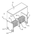
この種のチョークコイルとして、特開平11−238636号公報記載のものが知られている。図14は、このチョークコイルの一例を示す斜視図である。チョークコイル100は、磁性体ボビン112と、巻線126,128と、磁性体連結部材134とを備えている。磁性体ボビン112は四角柱状の巻装部を有し、この巻装部の両端部にそれぞれ端フランジ部116,118が形成され、中央部に中央フランジ部120が形成されている。中央フランジ部120は、端フランジ部116,118より若干小さい正方形状をしている(図15参照)。
【0003】
端フランジ部116と中央フランジ部120との間の巻装部には、巻線126が巻回されている。端フランジ部118と中央フランジ部120との間の巻装部には、巻線128が巻回されている。さらに、板状の磁性体連結部材134が、端フランジ部116,118の外周面上に載置され、端フランジ部116の外周部と端フランジ部118の外周部を連結している。一方、この連結部材134と中央フランジ部120の外周面との間には間隙gが形成されている。
【0004】
【発明が解決しようとする課題】
しかしながら、従来のチョークコイル100は、大きな値のノーマルモード電流が流れると、磁気飽和現象が発生して、インダクタンスが減少し、ノーマルモードノイズの除去性能が低下する。これを解決するために従来は、端フランジ部116,118のサイズを大きくし、連結部材を中央フランジ部120から遠ざけて位置することで、磁気飽和現象の発生を抑制し、ノーマルモードノイズの除去性能を維持していた。しかし、この結果、チョークコイル100の高さ寸法が大きくなるという問題があった。
【0005】
そこで、本発明の目的は、磁気飽和現象が発生しにくくかつ低背化が可能なチョークコイルを提供することにある。
【0006】
【課題を解決するための手段】
以上の目的を達成するため、本発明に係るチョークコイルは、
(a)柱状の巻装部と、前記巻装部の両端部にそれぞれ設けた端フランジ部と、前記巻装部の中央部に設けた中央フランジ部とからなる磁性体ボビンと、
(b)前記巻装部の両端部に設けた前記端フランジ部を連結し、前記中央フランジ部との間に間隙を有する磁性体連結部材と、
(c)前記巻装部の一端側の前記端フランジ部と前記中央フランジ部との間に巻回される巻線と、
(d)前記巻装部の他端側の前記端フランジ部と前記中央フランジ部との間に巻回される巻線とを備え、
(e)前記巻線によって発生するノーマルモードの磁束が、前記中央フランジ部と前記磁性体連結部材と前記端フランジ部と前記巻装部に形成されるとともに、前記巻線によって発生するコモンモードの磁束が、前記磁性体連結部材と前記端フランジ部と前記巻装部に形成され、
(f)前記中央フランジ部の前記連結部材配置側の縁部に、前記中央フランジ部と前記連結部材との間のノーマルモードの電流による磁気抵抗を増加させるための凹部及び傾斜部のうちの少なくともいずれか一つが設けられていること、
を特徴とする。
【0007】
【作用】
中央フランジ部の連結部材配置側の縁部に凹部や傾斜部を設けることにより、中央フランジ部と連結部材との間のノーマルモードの電流による磁気抵抗が増加する。従って、大きな値のノーマルモードノイズ電流が流れても、磁気飽和現象が発生しにくいチョークコイルが得られる。
【0008】
【発明の実施の形態】
以下、本発明に係るチョークコイルの一実施形態について添付図面を参照して説明する。
【0009】
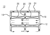
図1は、チョークコイル10の分解斜視図である。チョークコイル10は、磁性体ボビン12と巻線26,28と磁性体連結部材34とを備えている。磁性体ボビン12は、図2に示すように、四角柱状の巻装部14を有している。この巻装部14の両端部には、それぞれ矩形状の端フランジ部16,18が形成されている。また、巻装部14の中央部には、中央フランジ部20が形成されている。この中央フランジ部20は、端フランジ部16,18より若干小さい矩形状のものであって、隣接する二つの角部に傾斜部20aを有している。この傾斜部20aは、巻線26,28が中央フランジ部20からはみ出さないようにしながら、中央フランジ部20の上端の幅dを狭く、傾斜部20aの高さhを大きくすることで、ノーマルモードのノイズ電流による磁気抵抗を大きくするためのものである。従って、傾斜部20aの上端29aの位置は、巻線26の側面26aの位置よりも内側で、かつ、傾斜部20aの下端29bの位置は、巻装部14の巻芯の上面14aの位置より下側になるように設定されるのが好ましい(図5参照)。
【0010】
端フランジ部16には、二つの角部に電極22a,22bが形成されている。電極22a,22bは、端フランジ部16の両面に回り込むように形成される。また、端フランジ部18には、二つの角部に電極24a,24bが形成されている。電極24a,24bは、端フランジ部18の両面に回り込むように形成される。ここで、電極22aと電極24bとが対向する位置に形成され、電極22bと電極24aとが対向する位置に形成される。ボビン12は、例えばNi−Zn又は、Mg−Znなどの絶縁性の高いフェライト材料やそれらを含んだ磁性樹脂等で形成される。
【0011】
図1に示すように、端フランジ部16と中央フランジ部20との間の巻装部14には、巻線26が巻回されている。巻線26の両端は、電極22a,22bに接続される。さらに、端フランジ部18と中央フランジ部20との間の巻装部14には、巻線28が巻回されている。巻線28の両端は、電極24a,24bに接続される。巻線26は、端フランジ部16側からみて、例えば、電極22a側から電極22b側に向かって左回りとなるように形成される。このとき、巻線28は、端フランジ部18側からみて、電極24b側から電極24a側に向かって右回りとなるように形成される。
【0012】
さらに、板状の磁性体連結部材34が、図3〜図5に示すように、端フランジ部16,18の外周面上に載置され、端フランジ部16の外周部と端フランジ部18の外周部とを連結している。一方、この連結部材34と中央フランジ部20の外周面との間には間隙gが形成されている。
【0013】
図6は以上の構成からなるチョークコイル10の電気等価回路図である。図6において、30は、コモンモードの電流に対するインダクタンスを表わし、32はノーマルモードの電流に対するインダクタンスを表わしている。
【0014】
このチョークコイル10は、巻線26と巻線28とが中央フランジ部20で分割されていることにより、巻線26及び巻線28によって生じる磁束が重なり合わない。そのため、ノーマルモードの電流によって生じる磁束が打ち消し合わず、ノーマルモードの電流に対しても、インダクタンスを得ることができる。したがって、このチョークコイル10は、コモンモードノイズのみならず、ノーマルモードノイズも除去することができる。さらに、巻線26と巻線28とが分割されているため、これらの巻線26と巻線28の間において良好な耐電圧性を得ることができる。
【0015】
さらに詳しくこのチョークコイル10のコモンモードノイズ及びノーマルモードノイズの除去作用について説明する。
【0016】
このチョークコイル10を用いる場合、例えば電極22aと電極24bに信号源が接続され、電極22bと電極24aに負荷が接続される。そして、巻線26に往路の電流が流され、巻線28に復路の電流が流される。ここで、コモンモードノイズが流れる場合、巻線26,28には、同相のノイズ電流が流れる。このノイズ電流によって、巻線26及び巻線28の周囲に磁束が発生するが、これらの磁束は中央フランジ部20で打ち消し合うため、図7に矢印で示すように、全体として巻線26及び巻線28の両方を囲む磁束が得られる。
【0017】
このとき、連結部材34が端フランジ部16の外周部と端フランジ部18の外周部とを連結しているので、ボビン12と連結部材34とで閉磁路が形成され、コモンモードノイズ電流による磁束の磁気抵抗は低くなる。従って、コモンモードノイズ電流に対してインダクタンスを大きくすることができ、そのため、コモンモードノイズ電流に対してインピーダンスが高くなり、コモンモードノイズが効果的に除去される。
【0018】
また、ノーマルモードの電流によって発生する磁束は、図8に矢印で示すように、ボビン12内で打ち消し合わず、巻線26及び巻線28のそれぞれの周囲に形成される。つまり、それぞれの磁束は、ボビン12の両端部に設けた端フランジ部16,18から出て、中央部に設けられた中央フランジ部20に入る周回径路を採る。そして、連結部材34が磁路を形成している部分においては、連結部材34内を磁束が通る。この磁束によって巻線26及び巻線28にインダクタンスが生じ、このインダクタンスによってノーマルモードノイズが除去される。
【0019】
このとき、図5に示すように、中央フランジ部20は連結部材34側に傾斜部20aを有しているため、間隙gの実効的寸法が大きくなり、中央フランジ部20と連結部材34との間の磁気抵抗が増加する。これにより、中央フランジ部20から連結部材34を遠ざけることなく、ノーマルモードの電流による磁気抵抗が上がる。この結果、大電流が流れるところで使用する場合でも磁気飽和しにくく、有効にノーマルモードノイズを除去することができる。
【0020】
なお、本発明は、上記実施形態に限定されるものではなく、その要旨の範囲内で種々に変更することができる。特に、中央フランジ部20に設ける凹部や傾斜部の形状は任意である。例えば、図9に示すように、中央フランジ部20の二つの角部に円弧状の傾斜部20bを設けてもよい。
【0021】
また、図10や図11に示すように、中央フランジ部20の二つの角部に傾斜部20aを設けるとともに、連結部材34側の一辺の中央部に矩形状凹部20cや半円形状凹部20dを設けてもよい。これにより、図10や図11に示している中央フランジ部20と連結部材34との間の、ノーマルモードのノイズ電流による磁気抵抗が、図5に示している中央フランジ部20の場合と比較して大きくなる。
【0022】
あるいは、図12や図13に示すように、中央フランジ部20の連結部材34側の一辺の中央部に半円形状凹部20eや三角形状凹部20fを設けてもよい。さらに、中央フランジ部20の形状は巻線26,28を分割できるサイズを有し、所望の磁気抵抗を有するものであれば前記実施形態の形状に限るものではない。
【0023】
また、連結部材34としては、板状のものに限らず、例えば筒状に形成することができる。この場合、巻線26及び巻線28の全体を覆うように、連結部材34が取り付けられる。このように、連結部材34の形状は任意に変更可能であり、端フランジ部16と18とを連結するように形成されていればよい。
【0024】
【発明の効果】
以上の説明から明らかなように、本発明によれば、巻装部の中央フランジ部に、連結部材との間に間隙を設け、さらに、凹部又は傾斜部の形状を形成したことにより、ノーマルモードの大電流による磁束に対して連結部材を中央フランジ部から遠ざけることなく磁気抵抗を調整し、磁束の飽和を防止することができる。これにより、チョークコイルを大型化しなくてすむ。また、従来と同程度の飽和特性しか必要としない場合であれば、中央フランジ部と連結部材の間隙を小さくすることができ、チョークコイル全体を低背化することができる。
【図面の簡単な説明】
【図1】本発明に係るチョークコイルの一実施形態を示す分解斜視図。
【図2】図1に示すチョークコイルに用いられる磁性体ボビンを示す斜視図。
【図3】図1に示したチョークコイルの外観斜視図。
【図4】図3のIV−IV断面図。
【図5】図3のV−V断面図。
【図6】図3に示すチョークコイルの電気等価回路図。
【図7】図1に示したチョークコイルによるコモンモードノイズ除去を説明するための磁気回路図。
【図8】図1に示したチョークコイルによるノーマルモードノイズ除去を説明するための磁気回路図。
【図9】他の実施形態を示す断面図。
【図10】別の他の実施形態を示す断面図。
【図11】さらに別の他の実施形態を示す断面図。
【図12】さらに別の他の実施形態を示す断面図。
【図13】さらに別の他の実施形態を示す断面図。
【図14】従来のチョークコイルの一例を示す斜視図。
【図15】図14のXV−XV断面図。
【符号の説明】
10…チョークコイル
12…磁性体ボビン
14…巻装部
16,18…端フランジ部
20…中央フランジ部
20a,20b…傾斜部
20c,20d,20e,20f…凹部
26,28…巻線
34…磁性体連結部材
g…間隙[0001]
BACKGROUND OF THE INVENTION
The present invention relates to a choke coil, and more particularly to a choke coil used when noise generated from an electronic device or the like or noise entering an electronic device or the like is removed.
[0002]
[Prior art]
As this type of choke coil, one disclosed in Japanese Patent Laid-Open No. 11-238636 is known. FIG. 14 is a perspective view showing an example of the choke coil. The
[0003]
A winding 126 is wound around the winding portion between the
[0004]
[Problems to be solved by the invention]
However, in the
[0005]
Accordingly, an object of the present invention is to provide a choke coil which is less likely to cause a magnetic saturation phenomenon and can be reduced in height.
[0006]
[Means for Solving the Problems]
In order to achieve the above object, a choke coil according to the present invention includes:
(A) a magnetic bobbin comprising a columnar winding portion, end flange portions provided at both ends of the winding portion, and a central flange portion provided at a central portion of the winding portion;
(B) connecting the end flange portions provided at both ends of the winding portion, and a magnetic body connecting member having a gap between the center flange portion;
(C) a winding wound between the end flange portion on one end side of the winding portion and the central flange portion;
(D) a winding wound between the end flange portion on the other end side of the winding portion and the central flange portion;
(E) A normal mode magnetic flux generated by the winding is formed in the central flange portion, the magnetic body connecting member, the end flange portion, and the winding portion, and a common mode magnetic flux generated by the winding. Magnetic flux is formed in the magnetic body connecting member, the end flange portion and the winding portion,
(F) At least one of a concave portion and an inclined portion for increasing a magnetic resistance due to a normal mode current between the central flange portion and the connecting member at an edge portion of the central flange portion on the connecting member arrangement side. That either one is provided,
It is characterized by.
[0007]
[Action]
By providing a concave portion or an inclined portion at the edge of the central flange portion on the connecting member arrangement side, the magnetic resistance due to the normal mode current between the central flange portion and the connecting member increases. Therefore, it is possible to obtain a choke coil in which a magnetic saturation phenomenon hardly occurs even when a large value of normal mode noise current flows.
[0008]
DETAILED DESCRIPTION OF THE INVENTION
Hereinafter, an embodiment of a choke coil according to the present invention will be described with reference to the accompanying drawings.
[0009]
FIG. 1 is an exploded perspective view of the
[0010]
The
[0011]
As shown in FIG. 1, a winding 26 is wound around the winding
[0012]
Further, as shown in FIGS. 3 to 5, the plate-like magnetic
[0013]
FIG. 6 is an electrical equivalent circuit diagram of the
[0014]
In the
[0015]
The action of removing the common mode noise and normal mode noise of the
[0016]
When the
[0017]
At this time, since the connecting
[0018]
Further, the magnetic flux generated by the current in the normal mode is formed around each of the winding 26 and the winding 28 without being canceled in the
[0019]
At this time, as shown in FIG. 5, since the
[0020]
In addition, this invention is not limited to the said embodiment, It can change variously within the range of the summary. In particular, the shape of the concave portion and the inclined portion provided in the
[0021]
Further, as shown in FIGS. 10 and 11,
[0022]
Alternatively, as shown in FIGS. 12 and 13, a semicircular recess 20 e and a triangular recess 20 f may be provided at the center of one side of the
[0023]
In addition, the connecting
[0024]
【The invention's effect】
As is clear from the above description, according to the present invention, the center flange portion of the winding portion is provided with a gap between the connecting member and the shape of the concave portion or the inclined portion. The magnetic resistance can be adjusted and the saturation of the magnetic flux can be prevented without moving the connecting member away from the central flange portion with respect to the magnetic flux caused by the large current. This eliminates the need to increase the size of the choke coil. In addition, if only saturation characteristics similar to those in the conventional case are required, the gap between the central flange portion and the connecting member can be reduced, and the entire choke coil can be reduced in height.
[Brief description of the drawings]
FIG. 1 is an exploded perspective view showing an embodiment of a choke coil according to the present invention.
2 is a perspective view showing a magnetic bobbin used in the choke coil shown in FIG.
3 is an external perspective view of the choke coil shown in FIG. 1. FIG.
4 is a cross-sectional view taken along the line IV-IV in FIG. 3;
5 is a VV cross-sectional view of FIG.
6 is an electrical equivalent circuit diagram of the choke coil shown in FIG. 3;
7 is a magnetic circuit diagram for explaining common mode noise removal by the choke coil shown in FIG. 1; FIG.
8 is a magnetic circuit diagram for explaining normal mode noise removal by the choke coil shown in FIG. 1; FIG.
FIG. 9 is a cross-sectional view showing another embodiment.
FIG. 10 is a sectional view showing another embodiment.
FIG. 11 is a sectional view showing still another embodiment.
FIG. 12 is a cross-sectional view showing still another embodiment.
FIG. 13 is a cross-sectional view showing still another embodiment.
FIG. 14 is a perspective view showing an example of a conventional choke coil.
15 is a cross-sectional view taken along the line XV-XV in FIG.
[Explanation of symbols]
DESCRIPTION OF
Claims (1)
前記巻装部の両端部に設けた前記端フランジ部を連結し、前記中央フランジ部との間に間隙を有する磁性体連結部材と、
前記巻装部の一端側の前記端フランジ部と前記中央フランジ部との間に巻回される巻線と、
前記巻装部の他端側の前記端フランジ部と前記中央フランジ部との間に巻回される巻線とを備え、
前記巻線によって発生するノーマルモードの磁束が、前記中央フランジ部と前記磁性体連結部材と前記端フランジ部と前記巻装部に形成されるとともに、前記巻線によって発生するコモンモードの磁束が、前記磁性体連結部材と前記端フランジ部と前記巻装部に形成され、
前記中央フランジ部の前記連結部材配置側の縁部に、前記中央フランジ部と前記連結部材との間のノーマルモードの電流による磁気抵抗を増加させるための凹部及び傾斜部のうちの少なくともいずれか一つが設けられていること、
を特徴とするチョークコイル。A magnetic bobbin comprising a columnar winding portion, end flange portions provided at both ends of the winding portion, and a central flange portion provided at a central portion of the winding portion;
Connecting the end flange portions provided at both ends of the winding portion, and a magnetic body connecting member having a gap with the central flange portion;
A winding wound between the end flange portion on one end side of the winding portion and the central flange portion;
A winding wound between the end flange portion on the other end side of the winding portion and the central flange portion;
A normal mode magnetic flux generated by the winding is formed in the central flange portion, the magnetic body connecting member, the end flange portion, and the winding portion, and a common mode magnetic flux generated by the winding is Formed on the magnetic body connecting member, the end flange portion and the winding portion;
At least one of a concave portion and an inclined portion for increasing a magnetic resistance due to a normal mode current between the central flange portion and the connecting member at an edge portion of the central flange portion on the connecting member arrangement side. One is provided,
A choke coil characterized by
Priority Applications (2)
| Application Number | Priority Date | Filing Date | Title |
|---|---|---|---|
| JP2000221401A JP3695295B2 (en) | 2000-07-21 | 2000-07-21 | choke coil |
| US09/911,025 US6525638B2 (en) | 2000-07-21 | 2001-07-23 | Choke coil |
Applications Claiming Priority (1)
| Application Number | Priority Date | Filing Date | Title |
|---|---|---|---|
| JP2000221401A JP3695295B2 (en) | 2000-07-21 | 2000-07-21 | choke coil |
Publications (2)
| Publication Number | Publication Date |
|---|---|
| JP2002043142A JP2002043142A (en) | 2002-02-08 |
| JP3695295B2 true JP3695295B2 (en) | 2005-09-14 |
Family
ID=18715810
Family Applications (1)
| Application Number | Title | Priority Date | Filing Date |
|---|---|---|---|
| JP2000221401A Expired - Fee Related JP3695295B2 (en) | 2000-07-21 | 2000-07-21 | choke coil |
Country Status (2)
| Country | Link |
|---|---|
| US (1) | US6525638B2 (en) |
| JP (1) | JP3695295B2 (en) |
Families Citing this family (24)
| Publication number | Priority date | Publication date | Assignee | Title |
|---|---|---|---|---|
| TW572584U (en) * | 2002-12-17 | 2004-01-11 | Delta Electronics Inc | EMI suppression device |
| JP2004260095A (en) * | 2003-02-27 | 2004-09-16 | Murata Mfg Co Ltd | Winding type common mode choke coil |
| JP3852778B2 (en) * | 2004-02-18 | 2006-12-06 | スミダコーポレーション株式会社 | Coil, antenna and transformer using the coil |
| US7598839B1 (en) | 2004-08-12 | 2009-10-06 | Pulse Engineering, Inc. | Stacked inductive device and methods of manufacturing |
| JP4525589B2 (en) * | 2005-12-26 | 2010-08-18 | Tdk株式会社 | Filter element |
| TWM371291U (en) * | 2009-03-03 | 2009-12-21 | Delta Electronics Inc | Transformer assembly |
| US9083157B2 (en) * | 2012-03-13 | 2015-07-14 | Gregory E. Leyh | Collapsible high-voltage electrical discharge generator |
| EP2709118A1 (en) * | 2012-09-14 | 2014-03-19 | Magnetic Components Sweden AB | Optimal inductor |
| CN103310947A (en) * | 2013-06-26 | 2013-09-18 | 华为技术有限公司 | Magnetic device |
| CN105144315B (en) | 2013-07-08 | 2017-10-13 | 株式会社村田制作所 | Coil component |
| TWI609387B (en) * | 2014-09-02 | 2017-12-21 | 乾坤科技股份有限公司 | Composite magnetic component |
| US9767953B2 (en) * | 2014-12-16 | 2017-09-19 | Abc Taiwan Electronics Corp. | Common mode filter and core thereof |
| JP6520187B2 (en) * | 2015-02-18 | 2019-05-29 | Tdk株式会社 | Coil parts |
| US20160247627A1 (en) * | 2015-02-24 | 2016-08-25 | Maxim Integrated Products, Inc. | Low-profile coupled inductors with leakage control |
| JP6558128B2 (en) * | 2015-08-03 | 2019-08-14 | Tdk株式会社 | Coil device |
| JP6819314B2 (en) * | 2017-01-23 | 2021-01-27 | Tdk株式会社 | Common mode filter and its manufacturing method |
| JP6966868B2 (en) * | 2017-05-02 | 2021-11-17 | 太陽誘電株式会社 | Magnetic coupling type coil parts |
| JP7091622B2 (en) * | 2017-09-08 | 2022-06-28 | Tdk株式会社 | Coil device |
| CN109961921A (en) * | 2017-12-23 | 2019-07-02 | 乾坤科技股份有限公司 | Coupling inductor and preparation method thereof |
| KR102463336B1 (en) * | 2018-02-22 | 2022-11-04 | 삼성전기주식회사 | Inductor array |
| US11521787B2 (en) * | 2018-06-19 | 2022-12-06 | Tdk Corporation | Coil component |
| US11424070B2 (en) * | 2018-06-19 | 2022-08-23 | Tdk Corporation | Coil component |
| CN109637785A (en) * | 2019-01-09 | 2019-04-16 | 东莞普思电子有限公司 | Network transformer and its method for laser welding |
| JP7404823B2 (en) * | 2019-11-29 | 2023-12-26 | Tdk株式会社 | coil device |
Family Cites Families (1)
| Publication number | Priority date | Publication date | Assignee | Title |
|---|---|---|---|---|
| JPH11238636A (en) | 1998-02-23 | 1999-08-31 | Murata Mfg Co Ltd | Choke coil for removing common mode noise and normal mode noise |
-
2000
- 2000-07-21 JP JP2000221401A patent/JP3695295B2/en not_active Expired - Fee Related
-
2001
- 2001-07-23 US US09/911,025 patent/US6525638B2/en not_active Expired - Fee Related
Also Published As
| Publication number | Publication date |
|---|---|
| US20020021201A1 (en) | 2002-02-21 |
| US6525638B2 (en) | 2003-02-25 |
| JP2002043142A (en) | 2002-02-08 |
Similar Documents
| Publication | Publication Date | Title |
|---|---|---|
| JP3695295B2 (en) | choke coil | |
| JP3063619B2 (en) | choke coil | |
| JPH07297055A (en) | Choke coil | |
| JPH07106140A (en) | Common mode choke coil | |
| JP2007243131A (en) | Reactor part | |
| JPH0766041A (en) | Inductor | |
| JP2585303Y2 (en) | Noise prevention choke coil | |
| JP3886048B2 (en) | Line filter | |
| JP3063653B2 (en) | choke coil | |
| US6545582B2 (en) | Magnetic core having an effective magnetic bias and magnetic device using the magnetic core | |
| JP3396908B2 (en) | Line filter | |
| JP3580061B2 (en) | choke coil | |
| JP2534897Y2 (en) | Common mode coil for noise filter | |
| JP2729848B2 (en) | AC reactor | |
| JP3106892B2 (en) | choke coil | |
| JP2599483B2 (en) | Line filter | |
| JPS5847692Y2 (en) | eccentric magnetic core | |
| JPH0711445Y2 (en) | Ferrite core | |
| JP3316008B2 (en) | Transformers and power supplies | |
| JPH08213251A (en) | Choke coil | |
| JP3801686B2 (en) | Power inductor | |
| JPS63228605A (en) | Inductance element | |
| JP2580367Y2 (en) | Choke coil for noise filter | |
| JP5187248B2 (en) | Winding parts | |
| JP3480207B2 (en) | choke coil |
Legal Events
| Date | Code | Title | Description |
|---|---|---|---|
| A977 | Report on retrieval |
Free format text: JAPANESE INTERMEDIATE CODE: A971007 Effective date: 20050207 |
|
| A131 | Notification of reasons for refusal |
Free format text: JAPANESE INTERMEDIATE CODE: A131 Effective date: 20050222 |
|
| A521 | Written amendment |
Free format text: JAPANESE INTERMEDIATE CODE: A523 Effective date: 20050420 |
|
| TRDD | Decision of grant or rejection written | ||
| A01 | Written decision to grant a patent or to grant a registration (utility model) |
Free format text: JAPANESE INTERMEDIATE CODE: A01 Effective date: 20050607 |
|
| A61 | First payment of annual fees (during grant procedure) |
Free format text: JAPANESE INTERMEDIATE CODE: A61 Effective date: 20050620 |
|
| R150 | Certificate of patent or registration of utility model |
Free format text: JAPANESE INTERMEDIATE CODE: R150 |
|
| FPAY | Renewal fee payment (event date is renewal date of database) |
Free format text: PAYMENT UNTIL: 20080708 Year of fee payment: 3 |
|
| FPAY | Renewal fee payment (event date is renewal date of database) |
Free format text: PAYMENT UNTIL: 20090708 Year of fee payment: 4 |
|
| FPAY | Renewal fee payment (event date is renewal date of database) |
Free format text: PAYMENT UNTIL: 20090708 Year of fee payment: 4 |
|
| FPAY | Renewal fee payment (event date is renewal date of database) |
Free format text: PAYMENT UNTIL: 20100708 Year of fee payment: 5 |
|
| FPAY | Renewal fee payment (event date is renewal date of database) |
Free format text: PAYMENT UNTIL: 20100708 Year of fee payment: 5 |
|
| FPAY | Renewal fee payment (event date is renewal date of database) |
Free format text: PAYMENT UNTIL: 20110708 Year of fee payment: 6 |
|
| LAPS | Cancellation because of no payment of annual fees |