JP3677911B2 - Method and apparatus for plating semiconductor wafer - Google Patents
Method and apparatus for plating semiconductor wafer Download PDFInfo
- Publication number
- JP3677911B2 JP3677911B2 JP34659796A JP34659796A JP3677911B2 JP 3677911 B2 JP3677911 B2 JP 3677911B2 JP 34659796 A JP34659796 A JP 34659796A JP 34659796 A JP34659796 A JP 34659796A JP 3677911 B2 JP3677911 B2 JP 3677911B2
- Authority
- JP
- Japan
- Prior art keywords
- plating
- semiconductor wafer
- tank
- plating solution
- outflow hole
- Prior art date
- Legal status (The legal status is an assumption and is not a legal conclusion. Google has not performed a legal analysis and makes no representation as to the accuracy of the status listed.)
- Expired - Fee Related
Links
Images


Classifications
-
- H—ELECTRICITY
- H01—ELECTRIC ELEMENTS
- H01L—SEMICONDUCTOR DEVICES NOT COVERED BY CLASS H10
- H01L2224/00—Indexing scheme for arrangements for connecting or disconnecting semiconductor or solid-state bodies and methods related thereto as covered by H01L24/00
- H01L2224/01—Means for bonding being attached to, or being formed on, the surface to be connected, e.g. chip-to-package, die-attach, "first-level" interconnects; Manufacturing methods related thereto
- H01L2224/10—Bump connectors; Manufacturing methods related thereto
- H01L2224/11—Manufacturing methods
Landscapes
- Electroplating Methods And Accessories (AREA)
Description
【0001】
【発明の属する技術分野】
本発明は、電解めっき法を用いて半導体ウエハ上にめっきを施す方法及びその装置に関する。特に、半導体ウエハ上にバンプ電極を形成する方法及びその装置に関する。
【0002】
【従来の技術】
従来、ウエハ上にはんだめっきを施し、はんだバンプを形成する技術では、例えば特開昭62−266851号公報に開示されている技術が知られている。この技術によるはんだバンプの形成方法を図6に示す。
この技術では、ウエハ基板11上にアルミパッド電極12及びパッシベーション膜13を形成し、このパッシベーション膜13上にバリアメタル14を形成する。そして、厚膜液状レジストやドライフィルムレジスト16を塗布及びラミネートを実施して現像した後、バリアメタル14を電極として電解めっきを施す。これによりアルミパッド電極12上にはんだバンプ電極15を形成する(図6(a))。
続いて、厚膜液状レジストやドライフィルムレジスト16を剥離すると共に、バリアメタル14をエッチングして除去することにより図6(b)に示される構造が得られる。さらに、リフロー工程を経て、図6(c)に示されるようにな半球上のバンプ構造が得られる。このようにしてはんだめっきによるはんだバンプ電極15の形成を行うことができる。
このようなはんだバンプの形成は、例えば図7に示す装置を用いて行われる。即ち、めっき槽21内にめっき液23を入れ、平板状のはんだ板(アノード)22と平板状のウエハ11とをそれらの面の方向が略重力方向となるように平行に対向配置してめっき液23内に浸し、めっき液23をめっき槽21の底部に設けられたスターラ24にて攪拌して層流を作り、めっき液23を電着面に供給する構成としている。
【0003】
【発明が解決しようとする課題】
しかしながら、上記開示技術では、ウエハ11とはんだ板22とがめっき液23中に略重力方向に平行に対向配置されているので、ウエハ11とはんだ板22との間に作用する電気力線25は、図8に示されるようにウエハ11の端部に集中し、その電流密度はウエハ11の平坦部の約3倍になるので、約3倍の電流が集中する。この結果、電流密度に応じて付着するはんだ量が増加し、ウエハ11の端部におけるバンプ径及びバンプ高さが平坦部に比べて大きくなってしまうという問題がある。さらに、Snイオンに比べてPbイオンの比重が大きいために上記開示技術を用いてバンプ電極を形成すると、重力の影響を受けてPbイオンが下に沈降してしまい、ウエハ11の重力方向の下側が上側に比べてはんだ組成(錫比)が小さくなる傾向にあり、バンプ電極を均一な組成比に形成することが困難である。
【0004】
従って、本発明は、上記課題に鑑み、ウエハ全体に渡りめっき組成を均一にすることを目的とする。又、他の発明の目的は、ウエハの端部に集中して作用する電気力線を緩和し、バンプ電極の径、高さを均一に形成できるようにすることである。
【0005】
【課題を解決するための手段】
上記の課題を解決するために、請求項1に記載の手段を採用することができる。この手段によると、流出孔を有する筒状のめっき槽を用い、めっき槽内にアノードとしてのめっき板を略水平に配設し、めっき板に対して重力方向の下部側にめっき板に対向させてカソードとしての半導体ウエハを略水平に配設する。こうして、めっき板と半導体ウエハとが略平行に配設される。流出孔は筒状のめっき槽の側面部の半導体ウエハに近接した位置であって半導体ウエハの上面の重力方向における高さと略等しい高さに形成され、めっき液を重力差により外部に流出させるものである。そして、めっき液に作用する重力を用いてめっき槽内において、めっき液の液位を調整することにより、流出孔近傍におけるめっき液の流速を所定速度に設定して、めっき液の層流を重力方向下向きに形成して、半導体ウエハに対して層流を形成しながら半導体ウエハにめっきを施す。
このめっき法により半導体ウエハを略水平方向に配設し、重力方向にめっき液の層流を形成してめっきを行うことで、半導体ウエハ上に均一な組成及び厚さの一定なめっきを形成することができる。又、半導体ウエハがめっき板に対して重力方向の下部側に配設してめっきを行うことにより、めっき時に発生する泡等の影響を受けることがなく、高品質なめっきを形成することが可能である。
【0006】
また、めっき板と半導体ウエハとが略平行に配設されることにより、半導体ウエハ上に形成されるめっきの組成及び厚さをより均一にすることができる。
更に、流出孔が半導体ウエハの上面の重力方向における高さと略等しい高さに設けられることにより、半導体ウエハ上にめっき液の層流を良好に形成することができる。
更に、めっき液の液位を調整することにより、流出孔近傍におけるめっき液の流速を所定速度に設定することができ、より良好な品質のめっきを得ることができる。
【0007】
【0008】
請求項2に記載の手段によれば、めっき液が満たされる筒状のめっき槽の底面部に略水平にカソードとしての半導体ウエハが配設され、半導体ウエハの側面部がめっき槽の側面部に近接している。又、めっき槽において、半導体ウエハに対して重力方向の上部側には半導体ウエハと対向してアノードとしてのめっき板が略水平に配置される。めっき槽の側面部には半導体ウエハに近接した位置に流出孔が設けられ、この流出孔から重力差によりめっき液が外部に流出し、流出しためっき液は循環供給手段によりめっき板に対して重力方向の上部側よりめっき槽内に帰還される。
この装置構成により、半導体ウエハの側面部とめっき槽の側面部とが近接して配置されるので、めっき槽及びその外側の空気の誘電率は水に比べて非常に小さく、半導体ウエハとめっき板との間に作用する電気力線はめっき槽の外部に漏れることがなく、見かけ上はめっき槽内のみに電気力線が作用する。よって、半導体ウエハの端部に作用する電気力線が低減し、半導体ウエハの端部における電流密度をその中央部における電流密度と同程度にすることができ、形成されるめっきの高さ及び径を均一に形成することが可能となる。又、半導体ウエハがめっき槽の底面部に配置されるので、半導体ウエハはめっき槽内のめっき液面に発生する泡等の影響を受けることがなく、良好な品質のめっきが得られる。
【0009】
更に、めっき板と半導体ウエハとが略平行に配設されることにより、めっきの高さ、径及び組成をより均一に形成できる。
更に、流出孔が半導体ウエハの上面の重力方向における高さと略等しい高さに設けられることにより、半導体ウエハ上にめっき液の層流を良好に形成することができる。
更に、めっき液の液位を調整することにより、流出孔近傍におけるめっき液の流速を所定速度に設定することができ、より良好な品質のめっきを得ることができる。
【0010】
請求項3に記載の手段によれば、半導体ウエハ及びめっき板が略円板状を成し、めっき槽が略円筒状を成すことにより、半導体ウエハの端部に集中して作用する電気力線をより緩和することができる。
【0011】
【0012】
請求項4に記載の手段によれば、スリット状の流出孔が周方向に設けられることにより、めっき槽内のめっき液を良好に流出させることができる。
【0013】
請求項5に記載の手段によれば、めっき板はメッシュ状に形成されることにより、めっき液がめっき板内を通過することができるので、めっき槽内におけるめっき液の流れが良くなり、より良好な層流を得ることできる。
【0014】
【0015】
請求項6に記載の手段によれば、めっき槽に供給されためっき液の一部が、めっき板に対して重力方向の上部側より外部に流出することにより、めっき液の外部への流出位置を所定の高さに設定しておけば、常に、めっき液の液位を一定に保持することができ、めっき液の流速を所定速度に容易に設定することが可能となる。
【0016】
請求項7に記載の手段によれば、流出孔の断面積を調整することにより、流出孔近傍におけるめっき液の流速を所定速度に設定することができる。
また、請求項8、9のようにめっき槽として樹脂材から成るものを用いれば、電気力線はめっき槽内のみに作用するので、ウエハの端部に電気力線が集中して作用することがなく、電解めっきによりウエハ上に形成されるバンプの高さ及び径をほぼ均一にすることができる。
【0017】
【発明の実施の形態】
以下、本発明を具体的な実施例に基づいて説明する。
図1は、本発明の具体的な実施例に係わる電極形成装置100の構成を示した模式図である。めっき槽1は、樹脂材(プラスチック)から成り、円筒形状を成し、底面部1aに対向して重力方向の上側に開口面部1cを有している。又、めっき槽1の側面部1bには、めっき液3を流出させるためにスリット状の流出孔4が周方向に複数個設けられている。
底面部1a上にはカソードとしてのウエハ(基板)6が配置され、電源10の陰極側と接続されている。流出孔4は、ウエハ6の上面部61の重力方向における高さと略等しい高さに設けられている。ウエハ6は、略円板状を成し、その上面部61には図2に示されるように所定のバンプ形成パターン6aが形成されている。又、ウエハ6の側面部は、めっき槽1の内側面に近接して配置されている。
アノードとしての40%Sn−60%Pbから成るめっき板2は、ウエハ6と略同等の形状を成し、ウエハ6に略平行に対向して配設され、電源10の陽極側と接続されている。このめっき板2は、メッシュ状を成し、複数個の孔部21が形成されており、ウエハ6に対向して開口面部1c側に配置され、その側面部がめっき槽1の内側面に近接している。
【0018】
めっき槽1の重力方向下方には貯水槽7が配置されており、流出孔4及び開口面部1cから重力により自然流出しためっき液3が蓄えられる。この貯水槽7には、管8、ポンプ5及び管9が接続されており、管9の吐出口はめっき槽1の開口面部1cに配置されている。これにより、ポンプ5により汲み上げられた貯水槽7内のめっき液3は、管9を介して開口面部1cよりめっき槽1内に供給される構成となっている。貯水槽7、ポンプ5及び管8、9が請求項でいうところの循環供給手段に相当する。ポンプ5は、貯水槽7内のめっき液3をめっき槽1内に供給できるだけの揚程を有していれば、渦巻型、往復型のいずれの型でもよい。
尚、この電極形成装置100では、管9により供給されためっき液3の一部が、めっき槽1の開口面部1cから外側面をつたってオーバーフローする構成としている。又、めっき液3は、遊離酸浴(アルカノールスルホン酸)又は硼弗酸浴から構成されている。
【0019】
この電極形成装置100では、管9よりめっき液3がめっき槽1内に供給されると、めっき液3はめっき板2の孔部を通って重力方向下方に流れ込み、めっき液3の一部は開口面部1cより側面部1bの外側面をつたってオーバーフローする。めっき槽1内のめっき液3は、ウエハ6の上面部61の重力方向における高さと略等しい高さに設けられた流出孔4から外部に流出する。流出孔4から流出しためっき液3と開口面部1cからオーバーフローしためっき液3は、貯水槽7内に蓄えられる。そして、ポンプ5により吸引され、管8、9を通って再びめっき槽1内に供給される。このようにめっき液3をめっき槽1内に循環供給しながら電解めっきを行うことにより、ウエハ6の上面部61にはんだバンプ電極が所定のパターンで形成される。
【0020】
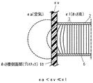
電極形成装置100では、円筒状のめっき槽1の底面部1aに略円板形状のウエハ6を、その側面部がめっき槽1の内側面に近接するように配置し、このウエハ6に対向してめっき板2を開口面部1c側に配置することにより、めっき槽1及びその外側の空気の誘電率εv 、εa がめっき液3の誘電率εl に比較して非常に小さく、εa <εv ≪εl の関係があることから、ウエハ6とめっき板2との間に作用する電気力線のめっき槽1の外部への漏れが小さくなる。このときのウエハ6とめっき板2との間に作用する電気力線の作用状態を図3に示すが、電気力線はめっき槽1内のみに作用するので、ウエハ6の端部に電気力線が集中して作用することがなく、電解めっきによりウエハ6上に形成されるバンプの高さ及び径をほぼ均一にすることができる。
又、ウエハ6がめっき槽1の底面部1aに平行に対向配置しているため、各部分での重力方向における高さが等しく、重力によるイオン分布密度が等しくなるため、従来の構成のようにウエハの重力方向の下側と上側とではんだ組成が異なることがなく、はんだ組成をほぼ均一に形成することが可能である。
又、ウエハ6がめっき槽1の底面部1aに配置されるので、電解めっき時にめっき液3の表面に発生する泡によるバンプ電極の形状不良を防止することができる。この泡は、ポンプ5によるもの、202-→O2+4e- の化学反応によりめっき時にアノード側から発生する酸素によるもの、2H+ +2e- →H2の化学反応によりカソード側から発生する水素によるものなどが考えられるが、ウエハ6を底面部1aに平行配置することで、これら泡による影響を排除することができる。
【0021】
又、流出孔4がウエハ6の上面部61の重力方向における高さと略等しい高さに設けられているので、重力による自然放出を用いているのでウエハ6上にめっき液3の層流を一様に形成することができ、バンプ電極の組成比の均一化及び厚さの均一化を図ることができる。
又、流出孔4近傍のめっき液3の流速は、めっき槽1内のめっき液3の液位を変化させることにより任意の速度に設定することができる。即ち、大気圧をPa、めっき液3の密度をρ、重力加速度をg、流出孔4近傍におけるめっき液3の流速をv、貯水槽7内のめっき液3の液位を基準としためっき槽1内におけるめっき液3の液位の高さをHとし、流出孔4の断面積sが開口面部1cの面積Sに比較して微小であると仮定すると、ベルヌーイの定理より式(1)が成立する。
【0022】
【数1】
Pa/ρ+gH= Pa/ρ+ (1/2)v2 ──(1)
【0023】
式(1)を流速vについて解くと式(2)が得られる。
【数2】
v = ( 2gH)1/2 ──(2)
【0024】
式(2)より、めっき槽1内のめっき液3の液位を変化させることで、流出孔4近傍におけるめっき液3の流速を所望の値に設定することができる。
又、本実施例では、めっき液3の一部が開口面部1cよりオーバーフローする構成としているので、常に、めっき液3の液位を一定に保持することができ、めっき槽1の高さを予め適切な値に設定しておけば、容易にめっき槽1内のめっき液3の液位を一定に保持することが可能である。
このように、めっき液3の一部を開口面部1cよりオーバーフローさせ、めっき液3の液位を一定に保持することで、流出孔4近傍のめっき液3の流速を所望の速度に保持することができる。これにより、ウエハ6上のめっき液3の層流速度を所望の値にすることでき、時間的に安定した層流を形成することができ、バンプ電極の品質向上に寄与することができる。
【0025】
上記の図1に示す電極形成装置100では、ウエハ6をその側面部をめっき槽1の側面部1bに近接して底面部1a上に配置し、側面部1bに流出孔4を設けた構成としたが、本発明はこれに限定されるものではない。
例えば、図4に上記実施例の変形例を示すが、めっき槽1の底面部1aの重力方向上方に金属から成り、円板状のサセプタ40を略水平に配設し、このサセプタ40上にウエハ6を配置する構成としてもよい。サセプタ40はめっき槽1の内径より小さい径を有し、上面に凹部41が形成され、この凹部41上にウエハ6が配置される。これによりウエハ6の周囲にサセプタ40の凸部42が配置される。サセプタ40とめっき槽1の側面部1bとの間には、めっき液3が通過できる通路43が設けられており、めっき槽1内のめっき液3は底面部1aに設けられた流出孔4から外部に流出される。このようにして電極形成装置101が形成されている。
【0026】
図4に示す構成とすることで、めっき板2とサセプタ40の周囲の凸部42との間にも電気力線が作用するので、めっき板2とウエハ6の端部との間に作用する電気力線を緩和することができ、ウエハ6の端部における電気力線密度を中央部における密度と略等しく均一にできる。この結果、バンプ電極の高さ及び径を均一に形成することができる。又、めっき槽1内のめっき液3はサセプサ40と側面部1bとの間の通路43を通って底面部1aに設けられた流出孔4から流出するので、めっき液3の重力による均一で一様な層流を形成することが可能である。このように図4に示す電極形成装置101により図1に示す装置100と同等の効果を得ることができる。
又、図4では、サセプタ40とめっき槽1の側面部1bとの間に通路43を設けた構成としたが、サセプタ40とめっき槽1との間に通路を設けず、サセプタ40の凸部42に貫通孔を設け、それを通路として用いてもよい。
【0027】
上記実施例では、スリット状の流出孔4を周方向に複数個設けた構成としたが、開口幅の大きい流出孔4を対向して設けた構成としてもよい。この場合のめっき槽1の模式的断面図を図5(a)に示す。
又、図5(b)にその模式的断面図を示すように比較的開口幅の大きい4つの流出孔4を略等間隔で設けた構成としてもよい。
【0028】
上記実施例では、主としてめっき槽1内のめっき液3の液位を調整することにより、流出孔4近傍のめっき液3の流速を所望の値に設定する構成としたが、所定断面積のオリフィスなどを流出孔4に装着して流出孔4の断面積を調整することで、めっき液3の流速を所望の値に設定する構成としてもよい。
又、上記実施例では、電極形成装置100を用いてはんだバンプ電極を形成する場合について説明したが、アルミニウム(Al)や銅(Cu)など他の金属材料を用いた電解めっき法によるバンプ電極形成に適用することができ、これにより他の組成から成るバンプ電極の高さ及び径を均一に形成することが可能となる。
尚、上記実施例では、めっき板2及び半導体ウエハ6を重力方向に対して直角となるように配置したが、これに限られるものではない。ウエハ6の表面に発生する泡がウエハ6の表面に滞留しない程度であれば、重力方向に対して斜めに配置してもよい。又、このような場合には、適宜ウエハ6を回転させることによりウエハ6の表面全体に略均一にめっき液が触れるようにすることが望ましい。
【0029】
上記に示されるように、本発明によれば、重力を用いてめっき液の層流を形成し、円筒状のめっき槽の底面部にウエハを水平配置し、そのウエハに対向してめっき板を重力方向の上方に水平配置することにより、めっき組成を均一にし、厚さを一様に形成することができる。又、別の発明によれば、ウエハの側面部をめっき槽の側面部に近接させることで、ウエハの端部に集中して作用する電気力線を緩和させ、ウエハ端部でのめっき厚さを中央部と略等しく均一に形成することができる。
【図面の簡単な説明】
【図1】 本発明の具体的な実施例に係わる電極形成装置の構成を示した模式図。
【図2】 本発明の具体的な実施例に係わる電極形成装置において、基板上に形成されるバンプの形成パターンを示した模式図。
【図3】 本発明の具体的な実施例に係わる電極形成装置において、めっき板とウエハとの間に作用する電気力線を示した模式図。
【図4】 本発明の具体的な他の実施例に係わる電極形成装置の構成を示した模式図。
【図5】 本発明の具体的な実施例に係わる電極形成装置において、めっき槽に形成された流出孔の変形例を示した模式的断面図。
【図6】 従来のバンプ電極の形成方法を示した模式図。
【図7】 従来の電極形成装置の構成を示した模式図。
【図8】 はんだ板とウエハとが平行配置されたときに作用する電気力線を示した模式図。
【符号の説明】
1 めっき槽
2 めっき板
3 めっき液
4 流出孔
5 ポンプ
6 ウエハ
7 貯水槽
8、9 管
10 電源
40 サセプタ
100、101 電極形成装置[0001]
BACKGROUND OF THE INVENTION
The present invention relates to a method and apparatus for plating a semiconductor wafer using an electrolytic plating method. In particular, the present invention relates to a method and apparatus for forming bump electrodes on a semiconductor wafer.
[0002]
[Prior art]
Conventionally, a technique disclosed in, for example, Japanese Patent Application Laid-Open No. 62-266851 is known as a technique for forming solder bumps by performing solder plating on a wafer. A method of forming solder bumps by this technique is shown in FIG.
In this technique, an
Subsequently, the thick film liquid resist or the dry film resist 16 is peeled off, and the
Such solder bumps are formed using, for example, an apparatus shown in FIG. That is, the
[0003]
[Problems to be solved by the invention]
However, in the above disclosed technique, since the
[0004]
Therefore, in view of the above problems, an object of the present invention is to make the plating composition uniform over the entire wafer. Another object of the present invention is to alleviate electric lines of force acting on the edge of the wafer so that the diameter and height of the bump electrodes can be formed uniformly.
[0005]
[Means for Solving the Problems]
In order to solve the above problems, the means described in
A semiconductor wafer is arranged in a substantially horizontal direction by this plating method, and a plating with a uniform composition and thickness is formed on the semiconductor wafer by forming a laminar flow of a plating solution in the gravity direction and performing plating. be able to. In addition, by placing the semiconductor wafer on the lower side in the direction of gravity with respect to the plating plate, it is possible to form high-quality plating without being affected by bubbles generated during plating. It is.
[0006]
Further, the plating plate and the semiconductor wafer are disposed substantially in parallel, whereby the composition and thickness of the plating formed on the semiconductor wafer can be made more uniform.
Furthermore, by providing the outflow hole at a height substantially equal to the height of the upper surface of the semiconductor wafer in the direction of gravity, a laminar flow of the plating solution can be satisfactorily formed on the semiconductor wafer.
Furthermore, by adjusting the liquid level of the plating solution, the flow rate of the plating solution in the vicinity of the outflow hole can be set to a predetermined speed, and plating with better quality can be obtained.
[0007]
[0008]
According to the means of claim 2 , the semiconductor wafer as the cathode is disposed substantially horizontally on the bottom surface of the cylindrical plating tank filled with the plating solution, and the side surface of the semiconductor wafer is disposed on the side surface of the plating tank. It is close. In the plating tank, a plating plate as an anode is disposed substantially horizontally facing the semiconductor wafer on the upper side in the gravity direction with respect to the semiconductor wafer. An outflow hole is provided in the side part of the plating tank close to the semiconductor wafer, and the plating solution flows out of the outflow hole due to the difference in gravity. Returned to the plating tank from the upper side of the direction.
With this apparatus configuration, since the side surface portion of the semiconductor wafer and the side surface portion of the plating tank are disposed close to each other, the dielectric constant of the plating tank and the air outside the plating tank is very small compared to water. The electric lines of force acting between them do not leak to the outside of the plating tank, and the electric lines of force act only in the plating tank. Therefore, the lines of electric force acting on the end portion of the semiconductor wafer are reduced, the current density at the end portion of the semiconductor wafer can be made comparable to the current density at the central portion, and the height and diameter of the plating formed Can be formed uniformly. In addition, since the semiconductor wafer is disposed on the bottom surface of the plating tank, the semiconductor wafer is not affected by bubbles or the like generated on the plating liquid surface in the plating tank, and good quality plating can be obtained.
[0009]
Furthermore, by arranging the plating plate and the semiconductor wafer substantially in parallel, the height, diameter and composition of plating can be formed more uniformly.
Furthermore, by providing the outflow hole at a height substantially equal to the height of the upper surface of the semiconductor wafer in the direction of gravity, a laminar flow of the plating solution can be satisfactorily formed on the semiconductor wafer.
Furthermore, by adjusting the liquid level of the plating solution, the flow rate of the plating solution in the vicinity of the outflow hole can be set to a predetermined speed, and plating with better quality can be obtained.
[0010]
According to the means of
[0011]
[0012]
According to the means of placing serial to claim 4, by a slit-shaped outflow holes are provided in the circumferential direction, it is possible to satisfactorily flows out of the plating solution in the plating tank.
[0013]
According to the means of
[0014]
[0015]
According to the means of
[0016]
According to the measures of
Further, if the plating tank is made of a resin material as in
[0017]
DETAILED DESCRIPTION OF THE INVENTION
Hereinafter, the present invention will be described based on specific examples.
FIG. 1 is a schematic diagram showing a configuration of an electrode forming apparatus 100 according to a specific embodiment of the present invention. The
A wafer (substrate) 6 as a cathode is disposed on the
A plated plate 2 made of 40% Sn-60% Pb as an anode has a shape substantially equivalent to that of the
[0018]
A
In the electrode forming apparatus 100, a part of the
[0019]
In this electrode forming apparatus 100, when the
[0020]
In the electrode forming apparatus 100, a substantially disc-shaped
Further, since the
In addition, since the
[0021]
In addition, since the
Further, the flow rate of the
[0022]
[Expression 1]
Pa / ρ + gH = Pa / ρ + (1/2) v 2 ── (1)
[0023]
Solving equation (1) for flow velocity v yields equation (2).
[Expression 2]
v = (2gH) 1/2 ─ (2)
[0024]
From equation (2), the flow rate of the
Further, in this embodiment, since a part of the
In this way, a part of the
[0025]
In the electrode forming apparatus 100 shown in FIG. 1 described above, the side surface of the
For example, FIG. 4 shows a modified example of the above embodiment. A plate-shaped
[0026]
With the configuration shown in FIG. 4, the lines of electric force also act between the plating plate 2 and the
In FIG. 4, the
[0027]
In the above embodiment, a plurality of slit-like outflow holes 4 are provided in the circumferential direction, but a configuration in which the outflow holes 4 having a large opening width are provided to face each other may be employed. A schematic cross-sectional view of the
Moreover, it is good also as a structure which provided the four
[0028]
In the above embodiment, the flow rate of the
Further, in the above-described embodiment, the case where the solder bump electrode is formed using the electrode forming apparatus 100 has been described. However, the bump electrode is formed by electrolytic plating using other metal material such as aluminum (Al) or copper (Cu). Thus, it becomes possible to uniformly form the height and diameter of the bump electrode made of another composition.
In the above embodiment, the plated plate 2 and the
[0029]
As shown above, according to the present invention, a laminar flow of a plating solution is formed using gravity, a wafer is horizontally disposed on the bottom surface of a cylindrical plating tank, and a plating plate is opposed to the wafer. By arranging horizontally above the direction of gravity, the plating composition can be made uniform and the thickness can be made uniform. Further, according to another invention, by bringing the side surface portion of the wafer close to the side surface portion of the plating tank, the electric lines of force acting on the edge portion of the wafer are relaxed, and the plating thickness at the wafer end portion is reduced. Can be formed substantially equally with the central portion.
[Brief description of the drawings]
FIG. 1 is a schematic diagram showing the configuration of an electrode forming apparatus according to a specific embodiment of the present invention.
FIG. 2 is a schematic diagram showing a bump formation pattern formed on a substrate in an electrode forming apparatus according to a specific embodiment of the present invention.
FIG. 3 is a schematic diagram showing lines of electric force acting between a plated plate and a wafer in an electrode forming apparatus according to a specific embodiment of the present invention.
FIG. 4 is a schematic diagram showing the configuration of an electrode forming apparatus according to another specific embodiment of the present invention.
FIG. 5 is a schematic cross-sectional view showing a modified example of an outflow hole formed in a plating tank in an electrode forming apparatus according to a specific embodiment of the present invention.
FIG. 6 is a schematic view showing a conventional bump electrode forming method.
FIG. 7 is a schematic diagram showing the configuration of a conventional electrode forming apparatus.
FIG. 8 is a schematic diagram showing lines of electric force acting when a solder plate and a wafer are arranged in parallel.
[Explanation of symbols]
DESCRIPTION OF
Claims (9)
流出孔を有する筒状のめっき槽を用い、
めっき槽内にアノードとしてのめっき板を略水平に配設し、
前記めっき板に対して重力方向の下部側に前記めっき板に対向させてカソードとしての前記半導体ウエハを略水平に配設し、
前記めっき板と前記半導体ウエハとが略平行に配設して、
前記流出孔は筒状のめっき槽の側面部の前記半導体ウエハに近接した位置であって前記半導体ウエハの上面の重力方向における高さと略等しい高さに形成され、前記めっき液を重力差により外部に流出させるものであり、
めっき液に作用する重力を用いて、めっき槽内において、めっき液の液位を調整することにより、前記流出孔近傍における前記めっき液の流速を所定速度に設定して、めっき液の層流を重力方向下向きに形成し、前記半導体ウエハに対して層流を形成しながら、前記半導体ウエハをめっきすること
を特徴とする半導体ウエハのめっき方法。In the method of plating a semiconductor wafer by electrolytic plating,
Using a cylindrical plating tank with an outflow hole,
A plating plate as an anode is disposed substantially horizontally in the plating tank ,
The semiconductor wafer as a cathode is disposed substantially horizontally facing the plating plate on the lower side in the direction of gravity with respect to the plating plate,
The plating plate and the semiconductor wafer are disposed substantially in parallel,
The outflow hole is formed at a position close to the semiconductor wafer on the side surface of the cylindrical plating tank and at a height substantially equal to the height of the upper surface of the semiconductor wafer in the direction of gravity. Is to be spilled into
By adjusting the level of the plating solution in the plating tank using the gravity acting on the plating solution, the flow rate of the plating solution in the vicinity of the outflow hole is set to a predetermined speed, and the laminar flow of the plating solution is reduced. A method of plating a semiconductor wafer, wherein the semiconductor wafer is plated while forming a laminar flow with respect to the semiconductor wafer.
めっき液が満たされ、カソードとしての前記半導体ウエハを略水平に配設する底面部と、前記半導体ウエハの側面部に近接した側面部とから成る筒状のめっき槽と、
前記めっき槽において、前記半導体ウエハに対して重力方向の上部側において、前記半導体ウエハと対向して略水平に配置されたアノードとしてのめっき板と、
前記めっき槽の前記側面部において、前記半導体ウエハに近接した位置に形成され、前記めっき液を重力差により外部に流出させる流出孔と、
前記流出孔から流出した前記めっき液を、前記めっき板に対して重力方向の上部側より前記めっき槽内に帰還させる循環供給手段と
から成り、
前記めっき板と前記半導体ウエハとが略平行に配設されており、
前記流出孔が、前記半導体ウエハの上面の重力方向における高さと略等しい高さに設けられ、
前記めっき液の液位を調整することにより、前記流出孔近傍における前記めっき液の流速が所定速度に設定された
ことを特徴とする半導体ウエハのめっき装置。In an apparatus for plating a semiconductor wafer by electrolytic plating,
A cylindrical plating tank that is filled with a plating solution and includes a bottom surface portion on which the semiconductor wafer as a cathode is disposed substantially horizontally, and a side surface portion close to the side surface portion of the semiconductor wafer;
In the plating tank, on the upper side in the direction of gravity with respect to the semiconductor wafer, a plating plate as an anode disposed substantially horizontally facing the semiconductor wafer;
In the side surface portion of the plating tank, formed at a position close to the semiconductor wafer, an outflow hole through which the plating solution flows out to the outside due to a gravitational difference,
The plating solution flowing out from the outflow hole, Ri consists the circulation and supply means for feeding back to the plating plate the plating tank from the top side of the gravity direction with respect to,
The plating plate and the semiconductor wafer are disposed substantially in parallel,
The outflow hole is provided at a height substantially equal to the height of the upper surface of the semiconductor wafer in the direction of gravity;
The semiconductor wafer plating apparatus , wherein a flow rate of the plating solution in the vicinity of the outflow hole is set to a predetermined speed by adjusting a liquid level of the plating solution .
Priority Applications (1)
| Application Number | Priority Date | Filing Date | Title |
|---|---|---|---|
| JP34659796A JP3677911B2 (en) | 1996-12-09 | 1996-12-09 | Method and apparatus for plating semiconductor wafer |
Applications Claiming Priority (1)
| Application Number | Priority Date | Filing Date | Title |
|---|---|---|---|
| JP34659796A JP3677911B2 (en) | 1996-12-09 | 1996-12-09 | Method and apparatus for plating semiconductor wafer |
Publications (2)
| Publication Number | Publication Date |
|---|---|
| JPH10172974A JPH10172974A (en) | 1998-06-26 |
| JP3677911B2 true JP3677911B2 (en) | 2005-08-03 |
Family
ID=18384513
Family Applications (1)
| Application Number | Title | Priority Date | Filing Date |
|---|---|---|---|
| JP34659796A Expired - Fee Related JP3677911B2 (en) | 1996-12-09 | 1996-12-09 | Method and apparatus for plating semiconductor wafer |
Country Status (1)
| Country | Link |
|---|---|
| JP (1) | JP3677911B2 (en) |
Families Citing this family (4)
| Publication number | Priority date | Publication date | Assignee | Title |
|---|---|---|---|---|
| US6547937B1 (en) * | 2000-01-03 | 2003-04-15 | Semitool, Inc. | Microelectronic workpiece processing tool including a processing reactor having a paddle assembly for agitation of a processing fluid proximate to the workpiece |
| US7390382B2 (en) | 2003-07-01 | 2008-06-24 | Semitool, Inc. | Reactors having multiple electrodes and/or enclosed reciprocating paddles, and associated methods |
| US7313462B2 (en) | 2003-06-06 | 2007-12-25 | Semitool, Inc. | Integrated tool with automated calibration system and interchangeable wet processing components for processing microfeature workpieces |
| US7393439B2 (en) | 2003-06-06 | 2008-07-01 | Semitool, Inc. | Integrated microfeature workpiece processing tools with registration systems for paddle reactors |
-
1996
- 1996-12-09 JP JP34659796A patent/JP3677911B2/en not_active Expired - Fee Related
Also Published As
| Publication number | Publication date |
|---|---|
| JPH10172974A (en) | 1998-06-26 |
Similar Documents
| Publication | Publication Date | Title |
|---|---|---|
| TWI345801B (en) | Electrochemical processing cell | |
| KR100616198B1 (en) | Electro-chemical deposition system and method of electroplating on substrates | |
| TWI572749B (en) | Control of electrolyte hydrodynamics for efficient mass transfer during electroplating | |
| US6524461B2 (en) | Electrodeposition of metals in small recesses using modulated electric fields | |
| TWI606154B (en) | Enhancement of electrolyte hydrodynamics for efficient mass transfer during electroplating | |
| US6989084B2 (en) | Semiconductor wafer plating cell assembly | |
| US20050279641A1 (en) | Plating method and apparatus that creates a differential between additive disposed on a top surface and a cavity surface of a workpiece using an external influence | |
| CN111094636B (en) | Method and apparatus for controlling delivery of cross-flow and impinging electrolyte during electroplating | |
| US20220018036A1 (en) | Low temperature direct copper-copper bonding | |
| KR19980079372A (en) | Mesh electrode and plating apparatus and plating method using the mesh electrode | |
| KR102563118B1 (en) | Convection Optimization for Mixed Feature Electroplating | |
| JP2008510889A (en) | Dynamic shape anode | |
| US20020108862A1 (en) | Electroplating apparatus with vertical electrical contact | |
| JP2004225129A (en) | Plating method and plating device | |
| KR102619843B1 (en) | Plating device and plating method | |
| JP3677911B2 (en) | Method and apparatus for plating semiconductor wafer | |
| JP2007308783A (en) | Apparatus and method for electroplating | |
| US20060163058A1 (en) | Apparatus for plating a semiconductor wafer and plating solution bath used therein | |
| JP5822212B2 (en) | Electrolytic plating equipment | |
| JPS62133097A (en) | Apparatus for plating semiconductor wafer | |
| KR100454505B1 (en) | Electroplating system with tilted ring | |
| US7025861B2 (en) | Contact plating apparatus | |
| JP3980809B2 (en) | Electrolytic treatment equipment | |
| KR20110097225A (en) | Apparatus for plate substrate | |
| JP3400278B2 (en) | Semiconductor manufacturing apparatus and semiconductor device manufacturing method |
Legal Events
| Date | Code | Title | Description |
|---|---|---|---|
| A977 | Report on retrieval |
Free format text: JAPANESE INTERMEDIATE CODE: A971007 Effective date: 20040210 |
|
| A131 | Notification of reasons for refusal |
Free format text: JAPANESE INTERMEDIATE CODE: A131 Effective date: 20040316 |
|
| A521 | Written amendment |
Free format text: JAPANESE INTERMEDIATE CODE: A523 Effective date: 20040514 |
|
| TRDD | Decision of grant or rejection written | ||
| A01 | Written decision to grant a patent or to grant a registration (utility model) |
Free format text: JAPANESE INTERMEDIATE CODE: A01 Effective date: 20050419 |
|
| A61 | First payment of annual fees (during grant procedure) |
Free format text: JAPANESE INTERMEDIATE CODE: A61 Effective date: 20050502 |
|
| R150 | Certificate of patent or registration of utility model |
Free format text: JAPANESE INTERMEDIATE CODE: R150 |
|
| FPAY | Renewal fee payment (event date is renewal date of database) |
Free format text: PAYMENT UNTIL: 20110520 Year of fee payment: 6 |
|
| LAPS | Cancellation because of no payment of annual fees |