JP2019201510A - Electric power conversion system - Google Patents
Electric power conversion system Download PDFInfo
- Publication number
- JP2019201510A JP2019201510A JP2018095912A JP2018095912A JP2019201510A JP 2019201510 A JP2019201510 A JP 2019201510A JP 2018095912 A JP2018095912 A JP 2018095912A JP 2018095912 A JP2018095912 A JP 2018095912A JP 2019201510 A JP2019201510 A JP 2019201510A
- Authority
- JP
- Japan
- Prior art keywords
- conversion unit
- phase
- terminal
- converter
- parallel
- Prior art date
- Legal status (The legal status is an assumption and is not a legal conclusion. Google has not performed a legal analysis and makes no representation as to the accuracy of the status listed.)
- Pending
Links
- 238000006243 chemical reaction Methods 0.000 title claims abstract description 181
- 239000004065 semiconductor Substances 0.000 abstract description 30
- 230000004048 modification Effects 0.000 description 17
- 238000012986 modification Methods 0.000 description 17
- 238000010586 diagram Methods 0.000 description 11
- 230000000052 comparative effect Effects 0.000 description 7
- 239000004020 conductor Substances 0.000 description 3
- 238000001816 cooling Methods 0.000 description 3
- 230000017525 heat dissipation Effects 0.000 description 3
- 238000004088 simulation Methods 0.000 description 3
- 230000008878 coupling Effects 0.000 description 2
- 238000010168 coupling process Methods 0.000 description 2
- 238000005859 coupling reaction Methods 0.000 description 2
- 239000000758 substrate Substances 0.000 description 2
- 230000002457 bidirectional effect Effects 0.000 description 1
- 230000005540 biological transmission Effects 0.000 description 1
- 230000000694 effects Effects 0.000 description 1
- 238000009429 electrical wiring Methods 0.000 description 1
- 230000005669 field effect Effects 0.000 description 1
- 238000000926 separation method Methods 0.000 description 1
Images


Landscapes
- Inverter Devices (AREA)
Abstract
Description
本発明の実施形態は、電力変換装置に関する。 Embodiments described herein relate generally to a power conversion apparatus.
交直変換を行う電力変換装置においては、大容量化などを目的として、複数の半導体素子を並列に接続する場合がある。複数の半導体素子を並列に接続する場合、各半導体素子に流れる電流を均等にするために、半導体素子に接続する配線の配線長や配線形状等を調整することが行われている(たとえば、特許文献1参照)。 In a power conversion device that performs AC / DC conversion, a plurality of semiconductor elements may be connected in parallel for the purpose of increasing capacity. When connecting a plurality of semiconductor elements in parallel, adjusting the wiring length, wiring shape, etc. of the wiring connected to the semiconductor elements is performed in order to equalize the current flowing through each semiconductor element (for example, patents). Reference 1).
しかしながら、並列運転するような半導体素子では、大電流が流れるため、近接して配置された半導体素子間の磁気結合の影響を無視することができない。並列運転する半導体素子を交流の相ごとにまとめて配置した上で、配線長や配線形状等による自己インダクタンスや相互インダクタンスを調整することによっては、電流を十分均等に配分することが困難である。 However, since a large current flows in a semiconductor element that operates in parallel, the influence of magnetic coupling between adjacent semiconductor elements cannot be ignored. It is difficult to distribute the current sufficiently evenly by adjusting the self-inductance and mutual inductance depending on the wiring length, wiring shape, etc. after arranging the semiconductor elements operated in parallel for each AC phase.
本発明の実施形態は、並列接続された半導体素子に流れる電流のアンバランスを低減した電力変換装置を提供する。 Embodiments of the present invention provide a power conversion device that reduces unbalance of currents flowing through semiconductor elements connected in parallel.
本発明の実施形態に係る電力変換装置は、第1電圧を有する直流電圧を入力し、または出力する第1直流端子と、前記第1電圧よりも低い第2電圧を有する直流電圧を入力し、または出力する第2直流端子と、第1相を有する交流を出力し、または入力する第1交流端子と、前記第1相と180°異なる第2相の交流を出力し、または入力する第2交流端子と、前記第1直流端子と前記第2直流端子との間に電気的に接続され前記第1交流端子に電気的に接続された第1ハーフブリッジ回路を含む第1変換部、および、前記第1変換部に隣接して配置され前記第1直流端子と前記第2直流端子との間に電気的に接続され前記第2交流端子に電気的に接続された第2ハーフブリッジ回路を含む第2変換部の第1の組と、前記第1ハーフブリッジ回路に電気的に並列接続された第3ハーフブリッジ回路を含む第3変換部、および、前記第3変換部に隣接して配置され前記第2ハーフブリッジ回路に電気的に並列接続された第4ハーフブリッジ回路を含む第4変換部の第2の組と、を備える。前記第1の組における前記第1変換部および前記第2変換部、ならびに、前記第2の組における前記第3変換部および前記第4変換部は、それぞれ第1方向に沿って配置される。 A power converter according to an embodiment of the present invention inputs a DC voltage having a first voltage, inputs a DC voltage having a first voltage, and inputs a DC voltage having a second voltage lower than the first voltage, Alternatively, the second DC terminal for outputting, the first AC terminal for outputting or inputting the alternating current having the first phase, and the second for outputting or inputting the alternating current of the second phase that is 180 ° different from the first phase. A first converter including an AC terminal, a first half-bridge circuit electrically connected between the first DC terminal and the second DC terminal and electrically connected to the first AC terminal; and A second half bridge circuit disposed adjacent to the first converter and electrically connected between the first DC terminal and the second DC terminal and electrically connected to the second AC terminal; A first set of second converters and the first half bridge A third converter including a third half-bridge circuit electrically connected in parallel to the path; and a fourth converter disposed adjacent to the third converter and electrically connected in parallel to the second half-bridge circuit. And a second set of fourth conversion units including a half-bridge circuit. The first conversion unit and the second conversion unit in the first set, and the third conversion unit and the fourth conversion unit in the second set are arranged along a first direction, respectively.
並列接続された半導体素子に流れる電流のアンバランスを低減した電力変換装置が提供される。 Provided is a power conversion device in which an imbalance of currents flowing through semiconductor elements connected in parallel is reduced.
以下に、各実施の形態について図面を参照しつつ説明する。
なお、図面は模式的または概念的なものであり、各部分の厚みと幅との関係、部分間の大きさの比率などは、必ずしも現実のものと同一とは限らない。また、同じ部分を表す場合であっても、図面により互いの寸法や比率が異なって表される場合もある。
なお、本願明細書と各図において、既出の図に関して前述したものと同様の要素には同一の符号を付して詳細な説明は適宜省略する。
Each embodiment will be described below with reference to the drawings.
The drawings are schematic or conceptual, and the relationship between the thickness and width of each part, the size ratio between the parts, and the like are not necessarily the same as actual ones. Further, even when the same part is represented, the dimensions and ratios may be represented differently depending on the drawings.
Note that, in the present specification and each drawing, the same elements as those described above with reference to the previous drawings are denoted by the same reference numerals, and detailed description thereof is omitted as appropriate.
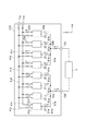
図1は、実施形態に係る電力変換装置を例示する模式的なブロック図である。
図1に表したように、電力変換装置10は、複数の第1相変換部21と、複数の第2相変換部22と、を備える。複数の第1相変換部21は、それぞれ並列に接続されている。複数の第2相変換部22は、それぞれ並列に接続されている。
FIG. 1 is a schematic block diagram illustrating a power conversion device according to an embodiment.
As illustrated in FIG. 1, the
電力変換装置10は、直流端子11p,11nと、交流端子12a,12bと、を含む。電力変換装置10は、直流端子11p,11nを介して図示しない直流回路に接続することができる。直流回路は、直流電源や、直流負荷、直流送電線等を含むことができる。
The
電力変換装置10は、交流端子12a,12bを介して、交流回路1に接続することができる。交流回路1は、交流電源や、交流負荷、電力系統等を含むことができる。電力変換装置10は、直流を交流に変換し、または交流を直流に変換して出力する。電力変換装置10は、直流と交流との双方向またはいずれか一方向の電力変換を行う。
The
後に詳述するが、第1相変換部21および第2相変換部22は、それぞれ同一のハーフブリッジ回路である。第1相変換部21および第2相変換部22は、180°の位相差で動作する。つまり、電力変換装置10は、直流を単相交流に変換し、あるいは、単相交流を直流に変換するフルブリッジ回路を含んでいる。第1相変換部21は、単相フルブリッジ回路の一方のレグであり、第2相変換部22は、他方のレグである。それぞれのレグを構成するアームについて、複数個のスイッチング素子が並列に接続されている。複数のスイッチング素子を並列に接続することによって、入出力電流の大電流化を実現する。
As will be described in detail later, the
交流の1/2周期においては、図の矢印で示したように、直流端子11pを介して、直流回路の高電位側から供給された電流は、第1相変換部21のハイサイド側スイッチング素子を介して、交流端子12aから出力される。電力変換装置10から出力された電流は、交流回路1を介して、交流端子12bに入力される。その交流電流は、第2相変換部22のローサイド側スイッチング素子を介して、直流端子11nに出力される。
In the half cycle of alternating current, as shown by the arrows in the figure, the current supplied from the high potential side of the direct current circuit via the
交流の次の1/2周期において、(図示しないが)直流端子11pを介して、直流回路の高電位側から供給された電流は、第2相変換部22のハイサイド側スイッチング素子を介して、交流端子12bから出力される。その交流電流は、第1相変換部21のローサイド側スイッチング素子を介して、直流端子11nに出力される。
In the next half cycle of the alternating current, the current supplied from the high potential side of the DC circuit via the
複数の第1相変換部21および複数の第2相変換部22は、ほぼ直線状に一列に配列されている。図1には、電力変換装置10の主要な構成要素が配置される位置や方向を示すために、二次元座標が設定されている。二次元座標は、X軸およびY軸を含む。X軸およびY軸は、直交する座標軸である。複数の第1相変換部21および複数の第2相変換部22は、X軸にほぼ平行な方向に一列に配列されている。後に詳述するが、複数の第1相変換部21および複数の第2相変換部22を並列に接続するためのブスバー(直流ブスバー31p,31n、交流ブスバー51a,51b)は、X軸にほぼ平行に設けられている。また、複数の第1相変換部21および複数の第2相変換部22と、ブスバーとを電気的に接続するため配線は、Y軸にほぼ平行な方向に設けられる。以下の説明では、このXY座標を用いることがある。
The plurality of
第1相変換部21は、端子21p,21n,21aを有する。第2相変換部22は、端子22p,22n,22bを有する。端子21p,21n,22p,22nは、直流電圧を入力し、または出力する端子である。端子21a,22bは、交流電圧を出力し、または入力する端子である。
The
端子21p,21n,21aおよび端子22p,22n,22bは、第1相変換部21および第2相変換部22において、それぞれ同じ位置に設けられている。好ましくは、複数の第1相変換部21および複数の第2相変換部22は、それぞれの端子がX軸方向に沿って配置されるように、一列に配列されている。
The
第1相変換部21は、第2相変換部22に隣接して配置されている。第1相変換部21および第2相変換部22が隣接配置された組を変換部ペア25と呼ぶ。変換部ペア25では、第2相変換部22は、第1相変換部21が配置された位置よりも、X軸の正方向よりの位置に配置されている。
The
なお、第1相変換部21が第2相変換部22に隣接して配置されるとは、変換部ペア25を構成する第1相変換部21と第2相変換部22との間に他の変換部が配置されていない場合をいうものとする。また、変形例において後述する第1相変換部21および第2相変換部22の位置関係が変換部ペア25と反対となる変換部ペア26についても、同様である。
The first
この例では、第1相変換部21および第2相変換部22の変換部ペア25は、X軸方向に沿って、4組順に配列されている。各変換部の符号で表すと、21,22,21,22,21,22,21,22の順に、X軸の正方向に向かって、一列に配列されている。
In this example, the conversion unit pairs 25 of the first
変換部ペア25では、第1相変換部21および第2相変換部22が隣接して配置されているので、端子21a,21bに流れる電流は、逆方向である。
In the
電力変換装置10は、直流ブスバー31p,31nを含む。直流ブスバー31p,31nは、ほぼ同一の長さ、幅および厚さを有する導電体により形成されている。直流ブスバー31p,31nは、長手方向がX軸方向にほぼ平行となるように設けられている。つまり、直流ブスバー31p,31nは、変換部ペア25の配列とほぼ平行となるように設けられている。
The
直流ブスバー31p,31nは、それぞれの形状や配置等に応じてインダクタンス成分を有する。このインダクタンス成分は、図では、破線で表されている。他の配線(交流ブスバー51a,51bおよび配線41p,41n,42p,42n,52a,52b)についても同様に、形状の応じたインダクタンス成分を有するが破線で示されている。
The DC bus bars 31p and 31n have inductance components according to their shapes and arrangements. This inductance component is represented by a broken line in the figure. Similarly, other wirings (AC bus bars 51a and 51b and
この例では、直流ブスバー31p,31nの一端に直流端子11p,11nが接続されている。直流ブスバー31pには、直流端子11pを介して、直流電圧が供給され、または、直流ブスバー31pから、直流端子11pを介して、直流電圧が出力される。直流ブスバー31nには、直流ブスバー31pよりも低い電圧を有する直流電圧が供給され、または、直流ブスバー31nから、直流端子11nを介して、直流ブスバー31pよりも低い電圧を有する直流電圧が出力される。
In this example,
直流ブスバー31p,31nと、第1相変換部21の端子21p,21nとの間に配線41p,41nが設けられている。直流ブスバー31p,31nと、第2相変換部22の端子22p,22nとの間に配線42p,42nが設けられている。配線41p,41nおよび配線42p,42nは、ほぼ同一の長さ、幅および厚さを有する導電体により形成されている。配線41p,41n,42p,42nは、この例では、長手方向がY軸にほぼ平行となるように設けられている。つまり、配線41p,41n,42p,42nは、直流ブスバー31p,31nとほぼ直交するように設けられている。
なお、直流ブスバー31p,31nおよび配線41p,41n,42p,42nは、異なる部材によって形成されていてもよいし、同一の部材によって一体として形成されていてもよい。
Note that the
電力変換装置10は、交流ブスバー51a,51bを含む。交流ブスバー51a,51bは、ほぼ同一の長さ、幅および厚さを有する導電体により形成されている。交流ブスバー51a,51bは、長手方向がX軸にほぼ平行となるように設けられている。つまり、交流ブスバー51a,51bは、変換部ペア25の配列とほぼ平行となるように設けられている。
この例では、交流端子12aと交流ブスバー51aとの間に配線52aが設けられ、交流の第1相の電圧が交流端子12aから出力され、または交流の第1相の電圧が交流端子12aに入力される。交流端子12bと交流ブスバー51bとの間に配線52bが設けられ、交流の第2相の電圧が交流端子12bから出力され、または交流の第2相の電圧が交流端子12bに入力される。
In this example, a
第1相変換部21の端子21aと交流ブスバー51aとの間に配線61aが設けられている。第2相変換部22の端子22bと交流ブスバー51bとの間に配線61bが設けられている。配線61a,61bは、ほぼ同一の長さ、幅および厚さを有する。すべての配線61a,61bは、長手方向がY軸にほぼ平行となるように設けられている。
A
なお、交流ブスバー51a,51bおよび配線61a,61bは、異なる部材によって形成されていてもよいし、同一の部材によって一体として形成されていてもよい。
Note that the AC bus bars 51a and 51b and the
このように、4つの第1相変換部21および4つの第2相変換部22の直流側では、直流ブスバー31p,31nによって、すべての変換器が並列に接続されている。
Thus, on the DC side of the four
また、4つの第1相変換部21の交流側では、交流ブスバー51aによって、すべての第1相変換部21が並列に接続されている。4つの第2相変換部22の交流側では、交流ブスバー51bによって、すべての第2相変換部22が並列に接続されている。つまり、電力変換装置10では、各々4つの変換部によって、交流端子12a,12bから出力される交流電流または、交流端子12a,12bに入力される交流電流を分担する。
Further, on the AC side of the four
この例では、分担する交流電流ごとに、第1相変換部21および第2相変換部22が変換部ペア25を構成し、変換部ペア25では、第1相変換部21および第2相変換部22が隣接して配置されている。さらに、変換部ペア25が配置の方向をそろえて、X軸にほぼ平行になるように4組配列されている。
In this example, the first
なお、上述では、直流ブスバー31p,31nおよび交流ブスバー51a,51bは、X軸にほぼ平行であり、配線41p,41n,42p,42nおよび配線61a,61bは、Y軸にほぼ平行であるとしたが、これに限定されるものではない。これら配線の配置については、直流端子や交流端子等の外部との接続のための構造や、放熱のための構造等の制約等に応じて、適切な方向、形状で設けられる。
In the above description, the
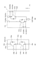
図2(a)は、実施形態の電力変換装置の一部を例示する回路図である。図2(b)は、図2(a)の回路を含むパワーモジュールを例示する模式図である。
第1相変換部21および第2相変換部22は、好ましくは、同一の入出力特性を有する半導体素子である。第1相変換部21および第2相変換部22をここでは半導体素子20と呼ぶ。
FIG. 2A is a circuit diagram illustrating a part of the power conversion device according to the embodiment. FIG. 2B is a schematic view illustrating a power module including the circuit of FIG.
The
図2(a)に示すように、半導体素子20は、スイッチング素子101a,101bと、ダイオード102a,102bと、を含む。スイッチング素子101a,101bは、直列に接続されている。ダイオード102a,102bは、スイッチング素子101a,101bにそれぞれ逆並列に接続されている。スイッチング素子101a,101bは、自己消弧型のスイッチング素子であり、たとえばIGBT(Insulated Gate Bipolar Transistor)やMOSFET(Metal-Oxide-Semiconductor Field-Effect Transistor)等である。
As shown in FIG. 2A, the
半導体素子20は、端子20p,20n,20aを含む。端子20pは、直列に接続され、高電位側のスイッチング素子101aの主電極(たとえば、コレクタ電極)に接続されている。端子20nは、直列に接続され、低電位側のスイッチング素子101bの主電極(たとえばエミッタ電極)に接続されている。端子20aは、スイッチング素子101a,101bの接続ノードに接続されている。
The
その他に、半導体素子20は、スイッチング素子101aの制御信号を入力するための端子20b,20cおよびスイッチング素子101bの制御信号を入力するための端子20d,20eを含む。端子20b,20cは、スイッチング素子101aの制御電極および主電極(たとえば、ゲート電極およびエミッタ電極)に接続され、端子20d,20eは、スイッチング素子101bの制御電極および主電極(たとえば、ゲート電極およびエミッタ電極)に接続されている。
In addition, the
図2(b)に示すように、半導体素子20は、パワーモジュールである。パワーモジュールである半導体素子20は、ケース110を有しており、ケース110内にスイッチング素子101a,101bおよびダイオード102a,102bが図示しない配線パターン付きの絶縁基板上に接続されている。絶縁基板上には、図2(a)の回路接続となるように、配線パターンが描かれている。
As shown in FIG. 2B, the
ケース110は、一方の面(図示しない面)に放熱のための放熱板が設けられている。ケース110は、放熱板が設けられた面を底面とするほぼ直方体であり、底面に対向する面(上面)に他の回路との電気的な接続をとるための端子C1,E2,C2E1が設けられている。端子C1は、端子20pに対応し、端子E2は、端子20nに対応し、端子C2E1は、端子20aに対応する。端子C1,E2は、上面を形成する方形面の1つの辺の近傍にその辺に沿って配置されている。端子C2E1は、端子C1,E2が配置された辺に対向する辺の近傍に配置されている。つまり、端子C1,E2が配置された側に直流ブスバー31p,31nが設けられ、端子C2E1が配置された側に交流ブスバー51a,51bが設けられることによって、もっとも短い距離で各配線の電気的な接続をとることができる。
The
この図のXY座標に示すように、半導体素子20は、端子C1,E2が設けられたケース110の縁を直流ブスバー31a,31bと平行になるように、配置される。この縁は、この場合には、端子C2E1が設けられたケース110の縁は、交流ブスバー51a,51bが設けられた側に沿うようになる。つまり、これらの縁がX軸にほぼ平行になるように半導体素子20が配置される。
As shown in the XY coordinates of this figure, the
半導体素子20は、放熱板の面を空冷または水冷の冷却フィンに接触させ熱的接続をとって配置される。X軸方向に平行な長手方向を有する冷却フィン上に複数の半導体素子20を一列に配列してもよいし、半導体素子20や変換部ペア25ごとに取り付けた冷却フィンをX軸方向に沿って、一列に配列するようにしてもよい。
The
すでに述べたように、半導体素子20は、X軸にほぼ平行になるように、一列に配置される。このとき、半導体素子20間の隣接する距離は、これに限定されないが、この例では、それぞれほぼ同じに設定される。半導体素子20間の隣接する距離は、変換部ペア内と変換部ペア間で変えてもよいし、同じにしてもよい。出力電流を各半導体素子20で均等にするためには、隣接距離間を等しくすることが好ましい。
As already described, the
本実施形態の電力変換装置10の効果について説明する。
以上説明したように、本実施形態の電力変換装置10では、第1相変換部21および第2相変換部22を隣接させて変換部ペア25を構成し、変換部ペア25を並列に接続することによって出力電流を向上させる。もっとも近く配置された第1相変換部21および第2相変換部22は、それぞれが入出力する交流電流が生成する磁界を互いに相殺するように動作するので、変換部ペア25同士の実質的なインダクタンスが小さくなり、並列に接続されたスイッチング素子101a,101bが分担する電流のばらつきが低減される。換言すると、逆位相の交流電流が流れる第1相変換部21および第2相変換部22を隣接させて配置することによって、半導体素子(パワーモジュール)内の配線等に生ずる相互インダクタンスが小さくなるため、全体のインダクタンスが小さくなり、分担する電流のばらつきが小さくなると考えられる。
The effect of the
As described above, in the
図3は、比較例の電力変換装置を例示する模式的なブロック図である。
図3に示すように、比較例の電力変換装置210は、4つの第1相変換部21と、4つの第2相変換部22と、を有しており、第1相変換部21および第2相変換部22は、すべてX軸方向にそって一列に配列されている。しかし、比較例の電力変換装置210では、第1相および第2相がそれぞれまとまって配置されており、第1相変換部21および第2相変換部22が隣接している組は、1組である。他の異なる相の変換部が隣接することはなく、同一相の変換部が並列に接続されている。
FIG. 3 is a schematic block diagram illustrating a power conversion device of a comparative example.
As illustrated in FIG. 3, the
比較例の場合には、第1相変換部21同士が隣接するようにまとまって一列に配置され、第2相変換部22同士が隣接するようにまとまって一列に配置されている。中央の第1相変換部21および第2相変換部22は隣接しているが、これらにそれぞれ並列に接続されている第1相変換部21および第2相変換部22は、いずれも互いに隣接して配置されていない。
In the case of the comparative example, the first
比較例の場合に、シミュレーションを用いて、各変換部から出力される交流電流のばらつきを評価したところ、素子によって、−50%程度〜+110%程度のばらつきがあることが確認されている。この場合のばらつきとは、出力電流を並列数で除した電流値(平均値)からの乖離を表している。つまり、ある素子では、平均値の+110%の電流が流れることとなる。 In the case of the comparative example, when the variation of the alternating current output from each converter is evaluated using simulation, it is confirmed that there is a variation of about −50% to + 110% depending on the element. The variation in this case represents a deviation from the current value (average value) obtained by dividing the output current by the parallel number. That is, in a certain element, a current of + 110% of the average value flows.
ブスバーや変換部同士の離間距離を同一の条件にして、実施形態の場合でシミュレーションを行うと、出力電流のばらつきは、−20%程度〜+10%程度となることが確認され、大幅に改善されている。 When the simulation is performed in the case of the embodiment under the same conditions for the bus bars and the separation distance between the conversion units, the variation in output current is confirmed to be about −20% to about + 10%, which is greatly improved. ing.
上述の実施形態では、交流の相ごとに4つの変換部を並列にする場合について説明したが、並列数は限定されるものではなく、2つ以上の変換部が並列接続されればよく、3つでもよいし、5つ以上であってもよい。以下に説明する変形例についても同様である。 In the above-described embodiment, the case where four conversion units are arranged in parallel for each AC phase has been described. However, the number of parallel units is not limited, and two or more conversion units may be connected in parallel. There may be one or more than five. The same applies to the modifications described below.
(変形例1)
図4は、変形例1に係る電力変換装置を例示する模式的なブロック図である。
図4に示すように、変形例1の電力変換装置310は、変換部ペア25のほかに、変換部ペア26を有する。変換部ペア26は、第1相変換部21および第2相変換部22を含み、第1相変換部21が第2相変換部22に隣接して配置されている。変換部ペア25と相違するのは、第1相変換部21および第2相変換部22の配置されている位置である。第2相変換部22は、第1相変換部21が配置された位置よりも、X軸の負方向よりの位置に配置されている。つまり、変換部ペア26では、変換部ペア25における第1相変換部21および第2相変換部22の位置が逆である。
(Modification 1)
FIG. 4 is a schematic block diagram illustrating a power converter according to the first modification.
As illustrated in FIG. 4, the
変形例1の電力変換装置310では、X軸の正方向に向かって、変換部ペア25、変換部ペア26、変換部ペア25、変換部ペア26の順に配列されている。各変換部の符号で表すと、21、22、22、21、21、22、22、21の順に配列されている。
In the
図1に示した実施形態および比較例の場合と同じ条件でシミュレーションを行うと、出力電流のばらつきは、−6%程度〜+6%程度に低減されることが確認されている。 When a simulation is performed under the same conditions as in the embodiment and the comparative example shown in FIG. 1, it has been confirmed that the variation in output current is reduced to about −6% to + 6%.
このように、出力する交流電流が逆位相で流れる変換部をペアにして、変換部ペア同士を並列に接続することによって、ペアにした変換部同士で交流電流に応じて生成された磁界をキャンセルして実質的なインダクタンスを低減することができる。そのため、分担される入出力電流のばらつきを小さくすることができる。 In this way, by converting converters that output alternating currents in opposite phases into pairs, and connecting the converter pairs in parallel, the magnetic fields generated according to the alternating currents between the paired converters are canceled. Thus, the substantial inductance can be reduced. Therefore, variation in the input / output current shared can be reduced.
(変形例2)
電力変換装置に含まれるすべての変換部について、逆位相のもの同士をペアにする場合に限らず、並列接続する変換部の一部について逆位相のもの同士をペアにしてもよい。
図5は、変形例2に係る電力変換装置を例示する模式的なブロック図である。
図5に示すように、本変形例の電力変換装置410では、並列数4に対して、3組の変換部ペアが設定されている。この例では、3組のうち、2組は変換部ペア25であり、残りの1組は変換部ペア26である。この例は、図3の変換部のうちX座標におけるもっとも小さい座標の位置から2番目の第1相変換部21と、8番目の第2相変換部22とを入れ替えた場合である。このように入れ替えた結果、X軸のもっとも小さい座標位置から、変換部ペア25、変換部ペア25、変換部ペア26の順で配置されている。
(Modification 2)
All the conversion units included in the power conversion device are not limited to pairing those having opposite phases, and those having opposite phases may be paired with respect to some of the conversion units connected in parallel.
FIG. 5 is a schematic block diagram illustrating a power converter according to the second modification.
As shown in FIG. 5, in the
(変形例3)
図6は、変形3に係る電力変換装置を例示する模式的なブロック図である。
図6に示すように、本変形例に係る電力変換装置510は、2組の変換部ペア25,26を含んでいる。この変形例では、並列数4に対して、2組の変換部ペアが設定されている。この例では、2組のうち、一方は変換部ペア25であり、他方は変換部ペア26である。この例は、図3の変換部のうちX座標のもっとも小さい座標の位置から4番目の第1相変換部21と、6番目の第2相変換部22とを入れ替えた場合である。
(Modification 3)
FIG. 6 is a schematic block diagram illustrating a power conversion device according to the third modification.
As shown in FIG. 6, the
交流の入出力電流の分担のばらつきは、各変換部が配置される間隔や、導電性のあるヒートシンクの形状、電流の大きさ、周波数等、多くのパラメータにより、誘導され相互作用する磁界の状況が異なる。そのため、結合状況による実際の電流のばらつきに応じて、適切な変換部ペアを設定し、配置を選択することができる。 The variation in the sharing of AC input / output current is due to the magnetic field induced and interacting with many parameters such as the spacing between each converter, the shape of the conductive heat sink, the current magnitude, and the frequency. Is different. Therefore, an appropriate conversion unit pair can be set and the arrangement can be selected according to the actual current variation due to the coupling state.
以上説明した実施形態によれば、並列接続された半導体素子に流れる電流のアンバランスを低減した電力変換装置を実現することができる。 According to the embodiment described above, it is possible to realize a power conversion device that reduces the unbalance of the current flowing through the semiconductor elements connected in parallel.
本発明のいくつかの実施形態を説明したが、これらの実施形態は、例として提示したものであり、発明の範囲を限定することは意図していない。これら新規な実施形態は、その他の様々な形態で実施されることが可能であり、発明の要旨を逸脱しない範囲で、種々の省略、置き換え、変更を行うことができる。これら実施形態やその変形は、発明の範囲や要旨に含まれるとともに、特許請求の範囲に記載された発明とその均等の範囲に含まれる。 Although several embodiments of the present invention have been described, these embodiments are presented by way of example and are not intended to limit the scope of the invention. These novel embodiments can be implemented in various other forms, and various omissions, replacements, and changes can be made without departing from the scope of the invention. These embodiments and modifications thereof are included in the scope and gist of the invention, and are included in the invention described in the claims and the equivalents thereof.
1 交流回路、10,310,410,510 電力変換装置、20 半導体素子、21 第1相変換部、22 第2相変換部、25,26 変換部ペア、31p,31n 直流ブスバー、41p,41n,42p,42n,51a,51b,61a,61b 配線、101a,101b スイッチング素子、102a,102b ダイオード、110 ケース
DESCRIPTION OF SYMBOLS 1
Claims (4)
前記第1電圧よりも低い第2電圧を有する直流電圧を入力し、または出力する第2直流端子と、
第1相を有する交流を出力し、または入力する第1交流端子と、
前記第1相と180°異なる第2相の交流を出力し、または入力する第2交流端子と、
前記第1直流端子と前記第2直流端子との間に電気的に接続され前記第1交流端子に電気的に接続された第1ハーフブリッジ回路を含む第1変換部、および、前記第1変換部に隣接して配置され前記第1直流端子と前記第2直流端子との間に電気的に接続され前記第2交流端子に電気的に接続された第2ハーフブリッジ回路を含む第2変換部の第1の組と、
前記第1ハーフブリッジ回路に電気的に並列接続された第3ハーフブリッジ回路を含む第3変換部、および、前記第3変換部に隣接して配置され前記第2ハーフブリッジ回路に電気的に並列接続された第4ハーフブリッジ回路を含む第4変換部の第2の組と、
を備え、
前記第1の組における前記第1変換部および前記第2変換部、ならびに、前記第2の組における前記第3変換部および前記第4変換部は、それぞれ第1方向に沿って配置された電力変換装置。 A first DC terminal for inputting or outputting a DC voltage having a first voltage;
A second DC terminal for inputting or outputting a DC voltage having a second voltage lower than the first voltage;
A first alternating current terminal for outputting or inputting alternating current having a first phase;
A second AC terminal that outputs or inputs an alternating current of a second phase that is 180 ° different from the first phase;
A first converter including a first half-bridge circuit electrically connected between the first DC terminal and the second DC terminal and electrically connected to the first AC terminal; and the first converter 2nd conversion part including the 2nd half bridge circuit arrange | positioned adjacent to a part and electrically connected between the said 1st DC terminal and the said 2nd DC terminal, and being electrically connected to the said 2nd AC terminal The first set of
A third converter including a third half-bridge circuit electrically connected in parallel to the first half-bridge circuit; and an electrical parallel to the second half-bridge circuit disposed adjacent to the third converter. A second set of fourth converters including a connected fourth half-bridge circuit;
With
The first conversion unit and the second conversion unit in the first set, and the third conversion unit and the fourth conversion unit in the second set are arranged along the first direction, respectively. Conversion device.
前記第3の組における前記第5変換部および前記第6変換部は、前記第1方向に沿って配置された請求項1〜3のいずれか1つに記載の電力変換装置。 A fifth converter including a fifth half-bridge circuit electrically connected in parallel to the first half-bridge circuit; and an electrical converter parallel to the second half-bridge circuit disposed adjacent to the fifth converter. A third set including a sixth conversion unit including a connected sixth half-bridge circuit;
The power converter according to any one of claims 1 to 3, wherein the fifth conversion unit and the sixth conversion unit in the third set are arranged along the first direction.
Priority Applications (1)
| Application Number | Priority Date | Filing Date | Title |
|---|---|---|---|
| JP2018095912A JP2019201510A (en) | 2018-05-18 | 2018-05-18 | Electric power conversion system |
Applications Claiming Priority (1)
| Application Number | Priority Date | Filing Date | Title |
|---|---|---|---|
| JP2018095912A JP2019201510A (en) | 2018-05-18 | 2018-05-18 | Electric power conversion system |
Publications (1)
| Publication Number | Publication Date |
|---|---|
| JP2019201510A true JP2019201510A (en) | 2019-11-21 |
Family
ID=68612396
Family Applications (1)
| Application Number | Title | Priority Date | Filing Date |
|---|---|---|---|
| JP2018095912A Pending JP2019201510A (en) | 2018-05-18 | 2018-05-18 | Electric power conversion system |
Country Status (1)
| Country | Link |
|---|---|
| JP (1) | JP2019201510A (en) |
Citations (3)
| Publication number | Priority date | Publication date | Assignee | Title |
|---|---|---|---|---|
| JP2816692B2 (en) * | 1989-01-30 | 1998-10-27 | 高周波熱錬株式会社 | Current supply balance method to switching element |
| JP2018011400A (en) * | 2016-07-12 | 2018-01-18 | 富士電機株式会社 | Single phase inverter unit |
| JP2019134543A (en) * | 2018-01-30 | 2019-08-08 | 富士電機株式会社 | Power supply device |
-
2018
- 2018-05-18 JP JP2018095912A patent/JP2019201510A/en active Pending
Patent Citations (3)
| Publication number | Priority date | Publication date | Assignee | Title |
|---|---|---|---|---|
| JP2816692B2 (en) * | 1989-01-30 | 1998-10-27 | 高周波熱錬株式会社 | Current supply balance method to switching element |
| JP2018011400A (en) * | 2016-07-12 | 2018-01-18 | 富士電機株式会社 | Single phase inverter unit |
| JP2019134543A (en) * | 2018-01-30 | 2019-08-08 | 富士電機株式会社 | Power supply device |
Similar Documents
| Publication | Publication Date | Title |
|---|---|---|
| EP3203625B1 (en) | Electric power conversion apparatus | |
| US9722598B2 (en) | Semiconductor device | |
| JP3173512U (en) | Semiconductor device | |
| RU2690021C1 (en) | Current busbar arrangement | |
| JP6400201B2 (en) | Power semiconductor module | |
| JP6319509B2 (en) | Semiconductor device | |
| US20130242631A1 (en) | Power converter apparatus | |
| JP2014036509A (en) | Three-level power conversion device | |
| US10601341B2 (en) | Neutral point clamped multiple-level switching unit for voltage inverter or rectifier | |
| JP2011211784A (en) | Power conversion device | |
| JP2014042377A (en) | Power supply bus bar and power converter using the same | |
| JP2019201510A (en) | Electric power conversion system | |
| JP3896940B2 (en) | Semiconductor device | |
| EP2858230A1 (en) | Power conversion apparatus | |
| EP3562023B1 (en) | Power conversion device | |
| WO2019031211A1 (en) | Power conversion device | |
| JP6575072B2 (en) | Phase unit and three-level power converter using the same | |
| JP7309396B2 (en) | semiconductor equipment | |
| JP7418276B2 (en) | element module | |
| JP5994462B2 (en) | Inverter device | |
| JP5877020B2 (en) | Switch module for power converter | |
| JP2017055478A (en) | Switching circuit and power conversion device | |
| EP4297087A1 (en) | Power electronic module with parallely connected power electronic devices | |
| KR102664547B1 (en) | Circuit layout, redistribution board, module and method of fabricating a half-bridge circuit | |
| JP2014033118A (en) | Semiconductor module pair and semiconductor device |
Legal Events
| Date | Code | Title | Description |
|---|---|---|---|
| A621 | Written request for application examination |
Free format text: JAPANESE INTERMEDIATE CODE: A621 Effective date: 20200612 |
|
| A977 | Report on retrieval |
Free format text: JAPANESE INTERMEDIATE CODE: A971007 Effective date: 20210517 |
|
| A131 | Notification of reasons for refusal |
Free format text: JAPANESE INTERMEDIATE CODE: A131 Effective date: 20210521 |
|
| A521 | Request for written amendment filed |
Free format text: JAPANESE INTERMEDIATE CODE: A523 Effective date: 20210720 |
|
| A02 | Decision of refusal |
Free format text: JAPANESE INTERMEDIATE CODE: A02 Effective date: 20210810 |