JP2010205108A - Apparatus and program for processing information - Google Patents
Apparatus and program for processing information Download PDFInfo
- Publication number
- JP2010205108A JP2010205108A JP2009051638A JP2009051638A JP2010205108A JP 2010205108 A JP2010205108 A JP 2010205108A JP 2009051638 A JP2009051638 A JP 2009051638A JP 2009051638 A JP2009051638 A JP 2009051638A JP 2010205108 A JP2010205108 A JP 2010205108A
- Authority
- JP
- Japan
- Prior art keywords
- circuit configuration
- unit
- circuit
- config
- information processing
- Prior art date
- Legal status (The legal status is an assumption and is not a legal conclusion. Google has not performed a legal analysis and makes no representation as to the accuracy of the status listed.)
- Granted
Links
Images


Classifications
-
- G—PHYSICS
- G06—COMPUTING; CALCULATING OR COUNTING
- G06F—ELECTRIC DIGITAL DATA PROCESSING
- G06F15/00—Digital computers in general; Data processing equipment in general
- G06F15/76—Architectures of general purpose stored program computers
- G06F15/78—Architectures of general purpose stored program computers comprising a single central processing unit
- G06F15/7867—Architectures of general purpose stored program computers comprising a single central processing unit with reconfigurable architecture
Abstract
Description
本発明は、情報処理装置および情報処理プログラムに関する。 The present invention relates to an information processing apparatus and an information processing program.
特許文献1では、マルチプロセッサシステムにおいて、コンパイラにより処理対象となる入力プログラムから自動的に並列性を持つタスクを抽出し、各プロセッサユニットの特性に合わせて当該タスクを配置する技術が開示されている。
特許文献2では、再構成可能に相互結合される複数の演算ユニットを含むリコンフィギュラブル回路と、所定の処理を実行するよう構成される固定のロジック回路およびパラメータ設定により処理仕様を変更可能に構成されるパラメータ付専用ハードウェアの少なくとも一方である処理回路とを備える半導体集積回路が開示されている。この半導体集積回路では、リコンフィギュラブル回路と処理回路とに結合される接続変更可能なネットワークと、ネットワークを当該ネットワーク以外と結合するために当該ネットワークに接続される少なくとも2つのインタフェースを備えている。
In
本発明は、動的に回路が再構成される演算手段によって複数の情報処理を行うにあたり、再構成の時間を考慮した回路構成を行うことを目的とする。 An object of the present invention is to provide a circuit configuration that takes into account the time required for reconfiguration when performing a plurality of information processing operations by means of arithmetic means for dynamically reconfiguring a circuit.
本願請求項1に係る発明は、動的に回路が再構成される第1演算部を複数備える第1回路構成手段と、固定の回路から成る第2演算部を複数備える第2回路構成手段と、情報を処理するにあたり、情報処理にかかる時間に応じて前記第1回路構成手段の第1演算部による回路構成および前記第2回路構成手段の第2演算部による回路構成を制御する回路構成制御手段とを有する情報処理装置である。
The invention according to
本願請求項2に係る発明は、前記第1回路構成手段による第1演算部が、前記第2回路構成手段による第2演算部より演算回路の粒度が大きい請求項1記載の情報処理装置である。
The invention according to
本願請求項3に係る発明は、前記第1回路構成手段が、前記第2回路構成手段より短い時間で回路構成を変更する請求項1または2記載の情報処理装置である。
The invention according to
本願請求項4に係る発明は、前記第1回路構成手段の第1演算部が複数の演算回路によって構成され、前記第2回路構成手段の第2演算部が単一の演算回路によって構成される請求項1から3のうちいずれか1項に記載の情報処理装置である。
In the invention according to
本願請求項5に係る発明は、前記回路構成制御手段が、一の情報の処理結果を他の情報の処理に用いない情報処理を行う際には前記第1回路構成手段の第1演算部による回路構成を制御する請求項1から4のうちいずれか1項に記載の情報処理装置である。
In the invention according to
本願請求項6に係る発明は、前記回路構成制御手段が、一の情報の処理結果を他の情報の処理に用いる情報処理を行う際には前記第2回路構成手段の第2演算部による回路構成を制御を行う請求項1から5のうちいずれか1項に記載の情報処理装置である。
In the invention according to
本願請求項7に係る発明は、前記回路構成制御手段が、前記第1回路構成手段の複数の第1演算部のうち一部を用いた回路構成を制御する請求項1から6のうちいずれか1項に記載の情報処理装置である。
The invention according to
本願請求項8に係る発明は、前記回路構成制御手段が、前記第2回路構成手段の複数の第2演算部のうち一部を用いた回路構成を制御する請求項1から7のうちいずれか1項に記載の情報処理装置である。
The invention according to claim 8 of the present application is any one of
本願請求項9に係る発明は、前記回路構成制御手段が、前記第2回路構成手段を複数の領域に分割し、各々の領域について相異なる領域で情報処理を行っている間に自領域の回路構成を行うよう制御する請求項1から7のうちいずれか1項に記載の情報処理装置である。
In the invention according to claim 9 of the present application, the circuit configuration control unit divides the second circuit configuration unit into a plurality of regions, and performs information processing in different regions for each region. The information processing apparatus according to
本願請求項10に係る発明は、動的に回路が再構成される第1演算部を複数備える第1回路構成手段と、固定の回路から成る第2演算部を複数備える第2回路構成手段とを用いて情報を処理するにあたり、情報処理にかかる時間に応じて前記第1回路構成手段の第1演算部による回路構成および前記第2回路構成手段の第2演算部による回路構成を制御するステップを情報処理装置に実行させる情報処理プログラムである。
The invention according to
本願請求項1に係る発明よれば、第1回路構成手段および第2回路構成手段のそれぞれの利点を生かした回路構成を構築することが可能となる。 According to the first aspect of the present invention, it is possible to construct a circuit configuration that takes advantage of the advantages of the first circuit configuration unit and the second circuit configuration unit.
本願請求項2に係る発明よれば、第1回路構成手段および第2回路構成手段の粒度の相違によるそれぞれの利点を生かした回路構成を構築することが可能となる。 According to the second aspect of the present invention, it is possible to construct a circuit configuration that takes advantage of the respective advantages of the first circuit configuration unit and the second circuit configuration unit due to the difference in granularity.
本願請求項3に係る発明よれば、第1回路構成手段および第2回路構成手段の回路構成変更時間の相違によるそれぞれの利点を生かした回路構成を構築することが可能となる。 According to the third aspect of the present invention, it is possible to construct a circuit configuration that takes advantage of the advantages of the first circuit configuration unit and the second circuit configuration unit due to the difference in the circuit configuration change time.
本願請求項4に係る発明よれば、第1回路構成手段および第2回路構成手段の演算回路の単位の相違によるそれぞれの利点を生かした回路構成を構築することが可能となる。 According to the fourth aspect of the present invention, it is possible to construct a circuit configuration that takes advantage of the respective advantages of the units of the arithmetic circuit of the first circuit configuration means and the second circuit configuration means.
本願請求項5に係る発明よれば、一の情報を単独で処理する回路構成を構築するにあたり、第2回路構成手段で構築するより短い処理時間となる第1回路構成手段に構築した回路構成が可能となる。
According to the invention according to
本願請求項6に係る発明よれば、一の情報の処理結果を他の情報の処理に用いる情報処理を構築するにあたり、第1回路構成手段で構築するより短い処理時間となる第2回路構成手段に構築した回路構成が可能となる。 According to the sixth aspect of the present invention, in constructing information processing that uses the processing result of one information for processing of other information, the second circuit configuration means that has a shorter processing time than that constructed by the first circuit configuration means. The circuit configuration constructed in (1) becomes possible.
本願請求項7に係る発明よれば、情報処理に必要な回路構成を第1回路構成手段の全体で構築する場合に比べて切り替え時間の短い回路構成を構築することが可能となる。
According to the invention of
本願請求項8に係る発明よれば、情報処理に必要な回路構成を第2回路構成手段の全体で構築する場合に比べて切り替え時間の短い回路構成を構築することが可能となる。 According to the invention of claim 8 of the present application, it is possible to construct a circuit configuration having a short switching time as compared with a case where a circuit configuration necessary for information processing is constructed by the entire second circuit configuration means.
本願請求項9に係る発明よれば、第2回路構成手段の回路構成を並列的に行うことが可能となる。 According to the invention of claim 9 of the present application, the circuit configuration of the second circuit configuration means can be performed in parallel.
本願請求項10に係る発明よれば、情報処理にかかる時間に応じて第1回路構成手段および第2回路構成手段のそれぞれの利点を生かした回路構成を構築することが可能となる。 According to the tenth aspect of the present invention, it is possible to construct a circuit configuration that takes advantage of the respective advantages of the first circuit configuration unit and the second circuit configuration unit according to the time required for information processing.
以下、本発明を実施するための形態(以下、「実施形態」という。)について説明する。なお、説明は以下の順序で行う。
1.概略構成
2.ブロック構成
3.情報処理の流れ
4.回路構成例
5.スケジューリング
Hereinafter, modes for carrying out the present invention (hereinafter referred to as “embodiments”) will be described. The description will be given in the following order.
1.
<1.概略構成>
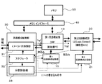
図1は、本実施形態に係る情報処理装置の概略構成を説明する図である。本実施形態に係る情報処理装置は、第1回路構成部10、第2回路構成部20および回路構成制御部30を備えている。
<1. Schematic configuration>
FIG. 1 is a diagram illustrating a schematic configuration of the information processing apparatus according to the present embodiment. The information processing apparatus according to the present embodiment includes a first
第1回路構成部10は、動的に回路が再構成される第1演算部を複数備えるもので、所定のタイミングで内部回路が再構成される、例えば、DRP(Dynamically Reconfigurable Processor)が用いられる。DRPは、クロック(数ナノ秒)単位で回路の再構成が成される。
The first
第1演算部の1つは、複数の演算回路によって構成されるプロセッサエレメント(PE)によって構成される。第1回路構成部10には、複数のプロセッサエレメントがマトリクス状に配置されており、プロセッサエレメントの組み合わせによって所定の情報処理回路が動的に構成される。
One of the first arithmetic units is configured by a processor element (PE) including a plurality of arithmetic circuits. In the first
第2回路構成部20は、固定の回路から成る第2演算部を複数備えるもので、所定のタイミングで内部回路が再構成される、例えば、FPGA(Field Programmable Gate Array)が用いられる。FPGAは、数クロック(数ミリ秒)単位で回路の再構成が成される。
The second
第2演算部の1つは、ANDゲート、ORゲート、加算器、減算器といった単一の演算回路(ロジックエレメント(LE)によって構成される。第2回路構成部20には、複数のロジックエレメントがマトリクス状に配置されており、ロジックエレメントの組み合わせによって所定の情報処理回路が動的に構成される。
One of the second arithmetic units is configured by a single arithmetic circuit (logic element (LE)) such as an AND gate, an OR gate, an adder, and a subtractor. The second
ここで、本実施形態では、プロセッサエレメントのような複数の演算回路を備えた第1演算部を粗粒度の演算器、ロジックエレメントのような単一の演算回路を備えた第2演算部を細粒度の演算器という。このような演算器の構成により、第1回路構成部10は、第2回路構成部20より短い時間で回路構成が変更されることになる。
Here, in the present embodiment, a first arithmetic unit having a plurality of arithmetic circuits such as processor elements is used as a coarse-grain arithmetic unit, and a second arithmetic unit including a single arithmetic circuit such as logic elements is subdivided. It is called a granularity calculator. With the configuration of such an arithmetic unit, the circuit configuration of the first
回路構成制御部は、所定の情報を処理するにあたり、情報処理にかかる時間に応じて第1回路構成部の第1演算部による回路構成および第2回路構成部の第2演算部による回路構成を制御する部分である。 When processing predetermined information, the circuit configuration control unit determines a circuit configuration by the first calculation unit of the first circuit configuration unit and a circuit configuration by the second calculation unit of the second circuit configuration unit according to the time required for information processing. The part to control.
回路構成制御部は、第1回路構成部であるDRPの特徴である高速での回路構成の利点と、第2回路構成であるFPGAの特徴である大規模回路の構成の利点とを考慮して、情報処理の全体として効率的な処理を行うための回路構成を制御する。 The circuit configuration control unit takes into account the advantages of the high-speed circuit configuration that is the feature of the DRP that is the first circuit configuration unit and the advantages of the configuration of the large-scale circuit that is the feature of the FPGA that is the second circuit configuration. Control the circuit configuration for performing efficient processing as a whole of information processing.
例えば、回路構成制御部は、一の情報の処理結果を他の情報の処理に用いない情報処理、すなわち、複数の情報について順次処理を行うにあたり、一の情報の処理結果を後の情報の処理にフィードバックするような処理を行わない場合には、第1回路構成部の第1演算部で回路構成するよう制御する。 For example, when the circuit configuration control unit performs information processing that does not use the processing result of one information for processing of other information, that is, sequentially processes a plurality of information, the processing result of one information In the case where the process that feeds back to is not performed, the first arithmetic unit of the first circuit configuration unit is controlled to configure the circuit.
また、回路構成制御部は、一の情報の処理結果を他の情報の処理に用いる情報処理、すなわち、複数の情報について順次処理を行うにあたり、一の情報の処理結果を後の情報の処理にフィードバックするような処理を行う場合には、第2回路構成部の第2演算部で回路構成するよう制御する。 In addition, the circuit configuration control unit uses information processing results of one information to process other information, that is, sequentially processes a plurality of pieces of information. In the case of performing processing such as feedback, control is performed so that the circuit is configured by the second calculation unit of the second circuit configuration unit.
回路構成制御部は、第1回路構成部や第2回路構成部の各々について、その全体もしくは一部を用いて回路構成を制御する。回路構成の情報は、情報処理装置に接続されるメモリに格納されている。回路構成制御部は、メモリインタフェースを介してメモリから回路構成の情報を読み出し、この回路構成の情報に基づき第1回路構成部および第2回路構成部の回路構成を制御する。なお、図1に示すメモリは、処理対象となる情報を一時記憶する記憶部と、回路構成の情報を記憶する回路構成記憶部とを共通で示している。 The circuit configuration control unit controls the circuit configuration of each of the first circuit configuration unit and the second circuit configuration unit using the whole or a part thereof. The circuit configuration information is stored in a memory connected to the information processing apparatus. The circuit configuration control unit reads circuit configuration information from the memory via the memory interface, and controls the circuit configurations of the first circuit configuration unit and the second circuit configuration unit based on the circuit configuration information. Note that the memory shown in FIG. 1 commonly shows a storage unit that temporarily stores information to be processed and a circuit configuration storage unit that stores circuit configuration information.
<2.ブロック構成>
図2は、本実施形態に係る情報処理装置のブロック構成図である。回路構成制御部30は、情報パス制御部31、スケジューラ32および分割制御部33を備える。情報パス制御部31は、処理対象となる情報の流れを制御する。すなわち、入力された情報を第1回路構成部や第2回路構成部に送る処理や、第1回路構成部および第2回路構成部とメモリとの間の情報の入出力を制御する。情報パス制御部31は、第1回路構成部10との間で情報の入出力を行う際、第1回路構成部10にトリガーTrg1を送る。また、第2回路構成部20との間で情報の入出力を行う際、第2回路構成部20にトリガーTrg2を送る。
<2. Block configuration>
FIG. 2 is a block configuration diagram of the information processing apparatus according to the present embodiment. The circuit
スケジューラ32は、パイプライン管理情報(管理テーブル)および第1回路構成部10および第2回路構成部20から送られる割り込み信号に基づき第1回路構成部10および第2回路構成部20の回路構成や情報の流れを制御する。また、スケジューラ32は、第1回路構成部10および第2回路構成部20の領域分割も制御する。
The
分割制御部33は、スケジューラ32の制御に基づき第1回路構成部10および第2回路構成部20の領域分割を指示する。スケジューラ32および分割制御部33は、第1回路構成記憶部11に指示を与え、第1回路構成記憶部11に記憶された回路構成を第1回路構成部10に与えて回路構成を行う。また、スケジューラ32および分割制御部33は、第2回路構成記憶部21に指示を与え、第2回路構成記憶部21に記憶された回路構成を第2回路構成部20に与えて回路構成を行う。
The
<3.情報処理の流れ>
[パイプライン]
図3は、情報処理のパイプラインを説明する図である。ここでは、情報処理として画像処理を例とし、1ピクセル(画素)ごと所定の画像処理を施す回路を例としている。また、図中「Config」は所定の処理回路の構成を示している。図3に示す例では、「Config−1」〜「Config−5」による回路構成が成され、「Config−1」〜「Config−4」が1ピクセル当たり1クロックでの処理、「Config−5」が1ピクセル当たり4クロックでの処理となっている。
<3. Information processing flow>
[pipeline]
FIG. 3 is a diagram for explaining an information processing pipeline. Here, image processing is taken as an example of information processing, and a circuit that performs predetermined image processing for each pixel (pixel) is taken as an example. In the figure, “Config” indicates the configuration of a predetermined processing circuit. In the example illustrated in FIG. 3, a circuit configuration of “Config-1” to “Config-5” is configured, and “Config-1” to “Config-4” are processed at one clock per pixel, “Config-5”. "Is processing at 4 clocks per pixel.
画像は1ピクセル単位で「Config−1」から「Config−2」の順に送られ、処理される。「Config−3」「Config−4」は並列処理され、「Config−5」に送られる。「Config−5」では、4クロックで1ピクセルの画像を処理する。 Images are sent and processed in the order of “Config-1” to “Config-2” in units of pixels. “Config-3” and “Config-4” are processed in parallel and sent to “Config-5”. In “Config-5”, an image of one pixel is processed in four clocks.
各Configでの処理時間は、ピクセル数とクロックの周波数とから計算される。例えば、JIS(日本工業規格)A4サイズ、600dpi(ドット/インチ)の画像情報の場合、合計32メガピクセルとなる。ここで、情報処理装置の動作クロックの周波数が200MHzの場合、1Configでの処理時間は32メガピクセル/200MHz=160msec(ミリ秒)となる。 The processing time in each Config is calculated from the number of pixels and the clock frequency. For example, in the case of image information of JIS (Japanese Industrial Standards) A4 size and 600 dpi (dot / inch), the total is 32 megapixels. Here, when the frequency of the operation clock of the information processing apparatus is 200 MHz, the processing time in 1 Config is 32 megapixels / 200 MHz = 160 msec (milliseconds).
[管理テーブル]
図4(a)は、パイプライン管理テーブルの例を示す図である。先に説明した画像情報のパイプライン処理を行うにあたり、スケジューラは図4(a)に示すパイプライン管理テーブルを用いて第1回路構成部の回路構成を行う。パイプライン管理テーブルには、回路構成であるConfig No.に対応して、使用するプロセッサエレメント(PE)の数、残りのPEの数、入力データ数(Input Stream Size)、出力データ数(OutPut Stream Size)、プロセッサタイプ、回路構成サイズ、レイテンシ(遅延クロック数)、処理時間が格納されている。スケジューラはこのパイプライン管理テーブルを参照して、回路構成の指示を行う。
[Management table]
FIG. 4A is a diagram illustrating an example of a pipeline management table. In performing the pipeline processing of the image information described above, the scheduler performs the circuit configuration of the first circuit configuration unit using the pipeline management table shown in FIG. In the pipeline management table, the Config No. Corresponding to the number of processor elements (PE) used, the number of remaining PEs, the number of input data (Input Stream Size), the number of output data (OutPut Stream Size), processor type, circuit configuration size, latency (delayed clock) Number), the processing time is stored. The scheduler refers to this pipeline management table and instructs the circuit configuration.
[選択テーブル]
図4(b)は、ロジックエレメントの(LE)の選択テーブルの例を示す図である。スケジューラは図4(b)に示す選択テーブルを用いて第2回路構成部の回路構成を行う。選択テーブルには、選択の優先順位に対応して、デバイス名、処理速度、書き換え時間、ロジックエレメント数(Gate bit)およびメモリ数が格納されている。スケジューラはこの選択テーブルを参照して、回路構成の指示を行う。すなわち、粗粒度の再構成可能回路(第1回路構成部)でレイテンシが発生する部分において、細粒度の再構成可能回路(第2回路構成部)へ置き換える場合、細粒度の再構成可能回路の候補をこのテーブルから選択する。その時にプライオリティ順に選択し、目標性能を達成するか判断する。
[Selection table]
FIG. 4B is a diagram illustrating an example of a selection table of (LE) of logic elements. The scheduler performs the circuit configuration of the second circuit configuration unit using the selection table shown in FIG. In the selection table, the device name, processing speed, rewrite time, number of logic elements (Gate bit), and number of memories are stored in correspondence with the priority of selection. The scheduler refers to this selection table and instructs the circuit configuration. That is, when a portion in which latency is generated in the coarse-grain reconfigurable circuit (first circuit configuration unit) is replaced with a fine-grain reconfigurable circuit (second circuit configuration unit), Select candidates from this table. At that time, the priority order is selected to determine whether the target performance is achieved.
粗粒度の再構成可能回路(第1回路構成部)と細粒度の再構成可能回路(第2回路構成部)とでは、基本的には粗粒度の再構成可能回路の方が高速処理でき、切換えも速い。しかし、粗粒度の再構成可能回路は、粒度が荒いため、帰還のかかった回路ではレイテンシが発生して、遅くなってしまう。一方、細粒度の再構成可能回路で論理合成すると、帰還回路は、1クロックで合成される。このため、粗粒度の再構成可能回路の欠点となる回路部分を細粒度の再構成可能回路で置き換えれば、各々の利点を生かし回路全体として高速化につながる。 The coarse-grain reconfigurable circuit (first circuit component) and the fine-grain reconfigurable circuit (second circuit component) can basically process the coarse-grain reconfigurable circuit faster. Switching is fast. However, since the coarse-grain reconfigurable circuit has a coarse granularity, latency is generated in the circuit to which feedback is applied, and the circuit becomes slow. On the other hand, when logic synthesis is performed with a fine-grain reconfigurable circuit, the feedback circuit is synthesized with one clock. For this reason, if the circuit portion which is a drawback of the coarse-grain reconfigurable circuit is replaced with a fine-grain reconfigurable circuit, the speed of the entire circuit can be increased by taking advantage of each advantage.
<4.回路構成例>
図5は、処理回路の構成による情報処理の流れを説明する図である。ここでは、回路構成の書き換えについて検討する。図5に示す例では、「Config−1」〜「Config−5」による回路構成が成され、「Config−1」「Config−2」「Config−4」が1ピクセル当たり1クロックでの処理、「Config−3」が1ピクセル当たり4クロックでの処理、「Config−5」が1ピクセル当たり3クロックでの処理となっている。
<4. Circuit configuration example>
FIG. 5 is a diagram for explaining the flow of information processing according to the configuration of the processing circuit. Here, rewriting of the circuit configuration is considered. In the example illustrated in FIG. 5, a circuit configuration of “Config-1” to “Config-5” is configured, and “Config-1”, “Config-2”, and “Config-4” are processed at one clock per pixel. “Config-3” is processing at 4 clocks per pixel, and “Config-5” is processing at 3 clocks per pixel.
この「Config−1」〜「Config−5」を全て第1回路構成部(例えば、DRP)で回路構成すると、1ピクセルの画像について「Config−1」〜「Config−5」を実行するにあたり、合計10クロック、つまり合計10回の回路構成の変更(書き換え)が必要となる。
When all of the “Config-1” to “Config-5” are configured by the first circuit configuration unit (for example, DRP), the “Config-1” to “Config-5” are executed for the image of one pixel. It is necessary to change (rewrite) the
これに対し、1ピクセル当たり複数クロックを要する「Config−3」と「Config−5」について、第2回路構成部(例えば、FPGA)で構成すると、それぞれ1ピクセル当たり1クロックで構成される可能性があるため、「Config−1」〜「Config−5」を実行するにあたり合計5クロックの処理で済むことになる。 On the other hand, if “Config-3” and “Config-5” that require multiple clocks per pixel are configured with the second circuit configuration unit (for example, FPGA), each clock may be configured with one clock per pixel. Therefore, processing of “Config-1” to “Config-5” only requires a total of 5 clocks.
図6は、回路の再構成回数と処理性能との関係を示す図である。図6では、A4サイズ、300dpiの画像情報について処理する際の回路再構成回数と処理能力(DPM:Document per minute)との関係をシミュレーションしたものである。このように、回路の再構成回数が少ないほど処理性能が高いことが分かる。 FIG. 6 is a diagram illustrating the relationship between the number of circuit reconfigurations and the processing performance. FIG. 6 shows a simulation of the relationship between the number of circuit reconfigurations and the processing capability (DPM: Document per minute) when processing image information of A4 size and 300 dpi. Thus, it can be seen that the smaller the number of circuit reconfigurations, the higher the processing performance.
一方、第2回路構成部では、大規模な回路構成は行えるものの、第1回路構成部ほど高速での回路の再構成には対応していない。図5に示す例では、「Config−3」および「Config−5」について第2回路構成部で回路構成を行うことで書き換え回数の低減を図っているが、第2回路構成部において「Config−3」から「Config−5」までの書き換え時間t2、および「Config−5」から「Config−3」までの書き換え時間t1を所定の許容時間内で行う必要がある。 On the other hand, although the second circuit configuration unit can perform a large-scale circuit configuration, the second circuit configuration unit does not support circuit reconfiguration at a higher speed than the first circuit configuration unit. In the example illustrated in FIG. 5, the number of rewrites is reduced by performing the circuit configuration in the second circuit configuration unit for “Config-3” and “Config-5”. However, in the second circuit configuration unit, “Config− The rewriting time t2 from “3” to “Config-5” and the rewriting time t1 from “Config-5” to “Config-3” need to be performed within a predetermined allowable time.
本実施形態では、このような観点から、高速で回路の再構成が行われる第1回路構成部と、大規模な回路の再構成に対応した第2回路構成部との両方を組み合わせ、情報処理の効率化を図るようにしている。 In the present embodiment, from such a viewpoint, both the first circuit configuration unit that performs high-speed circuit reconfiguration and the second circuit configuration unit that supports large-scale circuit reconfiguration are combined to perform information processing. To improve efficiency.
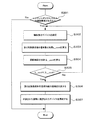
図7は、第1回路構成部および第2回路構成部の割り当て方法を説明するフローチャートである。先ず、所望の情報処理について、粗粒度の演算器を備えた第1回路構成部に回路構成を割り当てる(ステップS101)。この割り当てで情報処理の処理性能が所望の目標性能を達成しているか否かを判断する(ステップS102)。第1回路構成部へ回路を割り当てた際の処理性能は、図4(a)に示す管理テーブルを参照し、回路構成(Config)に対応したレイテンシと処理時間との積算によって求める。そして、この処理性能が目標性能に達しているか否かを判断する。目標性能に達している場合には第1回路構成部だけの回路構成とした割り当てで決定する。 FIG. 7 is a flowchart illustrating a method for assigning the first circuit configuration unit and the second circuit configuration unit. First, for desired information processing, a circuit configuration is assigned to a first circuit configuration unit including a coarse-grained arithmetic unit (step S101). It is determined whether or not the processing performance of information processing has achieved a desired target performance by this assignment (step S102). The processing performance when a circuit is assigned to the first circuit configuration unit is obtained by referring to the management table shown in FIG. 4A and integrating the latency corresponding to the circuit configuration (Config) and the processing time. Then, it is determined whether or not the processing performance has reached the target performance. When the target performance has been reached, it is determined by assignment with a circuit configuration of only the first circuit configuration unit.
一方、目標性能に達していない場合には、回路構成のパイプラインでのボトルネックを細粒度の演算器を備えた第2回路構成部に割り当てる(ステップS103)。そして、第2回路構成部へ回路構成を割り当てた状態での処理性能が目標性能に達しているか否かを判断する(ステップS104)。第2回路構成部へ回路構成を割り当てた際の処理性能は、図4(b)に示す選択テーブルを参照し、割り当てたデバイスの処理速度と書き換え時間との加算によって求める。また、残りの回路構成を第1回路構成部へ割り当てた際の処理性能と加算して全体の処理性能を求める。そして、この処理性能が目標性能に達しているか否かを判断する。目標性能に達している場合には第1回路構成部および第2回路構成部に回路構成を割り当てた構成で決定する。 On the other hand, if the target performance has not been reached, a bottleneck in the pipeline of the circuit configuration is assigned to the second circuit configuration unit having a fine-grained arithmetic unit (step S103). Then, it is determined whether or not the processing performance with the circuit configuration assigned to the second circuit configuration unit has reached the target performance (step S104). The processing performance when the circuit configuration is allocated to the second circuit configuration unit is obtained by referring to the selection table shown in FIG. 4B and adding the processing speed of the allocated device and the rewriting time. Further, the overall processing performance is obtained by adding the remaining circuit configuration to the processing performance when the first circuit configuration unit is assigned. Then, it is determined whether or not the processing performance has reached the target performance. When the target performance has been reached, it is determined by a configuration in which circuit configurations are assigned to the first circuit configuration unit and the second circuit configuration unit.
一方、目標性能に達していない場合には、粗粒度の演算器を備える第1回路構成部について、共通(常駐)回路の構成を細粒度の演算器を備える第2回路構成部に割り当てる処理を行う(ステップS105)。そして、共通(常駐)回路を第2回路構成部へ割り当てた状態での処理性能が目標性能に達しているか否かを判断する(ステップS106)。目標性能に達している場合には第1回路構成部および第2回路構成部に回路構成を割り当てた構成で決定する。 On the other hand, when the target performance has not been reached, a process of assigning the configuration of the common (resident) circuit to the second circuit configuration unit including the fine-grained arithmetic unit for the first circuit configuration unit including the coarse-grained arithmetic unit. This is performed (step S105). Then, it is determined whether or not the processing performance in a state where the common (resident) circuit is allocated to the second circuit configuration unit has reached the target performance (step S106). When the target performance has been reached, it is determined by a configuration in which circuit configurations are assigned to the first circuit configuration unit and the second circuit configuration unit.
一方、目標性能に達していない場合には、粗粒度の演算器を備えた第1回路構成部と、細粒度の演算器を備えた第2回路構成部との並列化を図り(ステップS107)、処理性能が目標性能に達しているか否かを判断する(ステップS108)。目標性能に達している場合にはこの回路構成の割り当てで決定する。一方、目標性能に達していない場合には、ステップS101へ戻り、目標性能の見直しを図り、その後の処理を繰り返す。 On the other hand, if the target performance has not been reached, parallelization of the first circuit configuration unit including the coarse-grained arithmetic unit and the second circuit configuration unit including the fine-grained arithmetic unit is attempted (step S107). Then, it is determined whether or not the processing performance has reached the target performance (step S108). When the target performance has been reached, it is determined by the assignment of this circuit configuration. On the other hand, if the target performance has not been reached, the process returns to step S101, the target performance is reviewed, and the subsequent processing is repeated.
図7に示す回路構成の割り当ては、主として情報処理装置の設計段階で行われ、所定の情報処理についての回路構成の割り当て、すなわち、所定の情報処理を行う際の第1回路構成部での回路構成および第2回路構成部での回路構成が、それぞれ図2に示す第1回路構成記憶部11および第2回路構成記憶部21に格納されることになる。
The assignment of the circuit configuration shown in FIG. 7 is mainly performed at the design stage of the information processing apparatus, and the assignment of the circuit configuration for the predetermined information processing, that is, the circuit in the first circuit configuration unit when performing the predetermined information processing The configuration and the circuit configuration in the second circuit configuration unit are respectively stored in the first circuit
<5.スケジューリング>
[第1のスケジューリング]
図8は、第1のスケジューリングを説明するフローチャートである。このフローチャートでの処理は、回路構成制御部30のスケジューラ32で実行される。先ず、所望の情報処理の回路構成(Config)で処理時間が所定の閾値を超えるものを抽出する(ステップS201)。回路構成の処理時間は、図4(a)に示す管理テーブルを参照することで行われる。例えば、この判断によって、回路構成中、フィードバック等の処理によって1ピクセル当たりの処理に1クロックを超えるレイテンシが発生しているものが抽出される。レイテンシが発生する回路構成(Config)が抽出されない場合は終了する。
<5. Scheduling>
[First scheduling]
FIG. 8 is a flowchart for explaining the first scheduling. The processing in this flowchart is executed by the
次に、1クロックを超えるレイテンシが発生する回路構成(Config)が抽出された場合、その回路構成について細粒度の演算器を備える第2回路構成部での回路構成を選択する(ステップS202)。この処理では、図4(b)に示す選択テーブルを参照し、優先順位の高い方から順にデバイス(細粒度の演算器の組み合わせ構成)が選択される。 Next, when a circuit configuration (Config) that generates a latency exceeding one clock is extracted, a circuit configuration in the second circuit configuration unit including a fine-grained arithmetic unit is selected for the circuit configuration (step S202). In this process, referring to the selection table shown in FIG. 4B, devices (combined configurations of fine-grained arithmetic units) are selected in order from the highest priority.
次に、選択されたデバイスを用いた場合の第2回路構成部の書き換え時間(t_conf)を算出する(ステップS203)。書き換え時間(t_conf)は、ロジックエレメント(LE)のゲートビット(Gate bit)×1ビット(bit)当たりの書き換え時間によって計算される。 Next, the rewrite time (t_conf) of the second circuit configuration unit when the selected device is used is calculated (step S203). The rewrite time (t_conf) is calculated by the rewrite time per gate bit (Gate bit) × 1 bit (bit) of the logic element (LE).
次に、各回路構成(Config)の間隔時間の合計Δ_confを算出する(ステップS204)。そして、書き換え時間(t_conf)が合計の間隔時間(Δ_conf)より小さいか否かの判断を行う(ステップS205)。ここで、書き換え時間(t_conf)が合計の間隔時間(Δ_conf)より小さい場合、選択されたデバイスで第2回路構成部の回路を構成する(ステップS206)。 Next, the sum Δ_conf of the interval time of each circuit configuration (Config) is calculated (step S204). Then, it is determined whether the rewrite time (t_conf) is shorter than the total interval time (Δ_conf) (step S205). Here, when the rewrite time (t_conf) is smaller than the total interval time (Δ_conf), the circuit of the second circuit configuration unit is configured by the selected device (step S206).
一方、書き換え時間(t_conf)が合計の間隔時間(Δ_conf)より小さくない場合、ステップS202へ戻り、次の優先順位のデバイスを選択テーブルから選択し、以降の処理を繰り返す。 On the other hand, if the rewrite time (t_conf) is not smaller than the total interval time (Δ_conf), the process returns to step S202, the next priority device is selected from the selection table, and the subsequent processing is repeated.
図9は、第1のスケジューリングを説明するパイプラインの流れ図である。図9に示す例では、「Config−1」〜「Config−5」による回路構成が成され、「Config−1」「Config−2」「Config−4」が1ピクセル当たり1クロックでの処理、「Config−3」が1ピクセル当たり4クロックでの処理、「Config−5」が1ピクセル当たり3クロックでの処理となっている。第1のスケジュールでは、このうち、1クロックを超えるレイテンシの発生する回路構成として「Config−3」が抽出される。 FIG. 9 is a pipeline flowchart illustrating the first scheduling. In the example illustrated in FIG. 9, a circuit configuration of “Config-1” to “Config-5” is configured, and “Config-1”, “Config-2”, and “Config-4” are processed at one clock per pixel. “Config-3” is processing at 4 clocks per pixel, and “Config-5” is processing at 3 clocks per pixel. In the first schedule, “Config-3” is extracted as a circuit configuration in which latency exceeding one clock occurs.
そして、抽出された「Config−3」を細粒度の演算器を備える第2回路構成部に割り当てた場合、処理時間は「Config−1」「Config−2」「Config−4」と同様の160msとなる。また、「Config−3」を第2回路構成部に割り当てた際の書き換え時間(t_conf)を計算する。そして、この書き換え時間(t_conf)と合計の間隔時間(Δ_conf)とを比較し、デバイスの決定を行う。 When the extracted “Config-3” is assigned to the second circuit configuration unit including the fine-grained arithmetic unit, the processing time is 160 ms, which is the same as “Config-1”, “Config-2”, and “Config-4”. It becomes. Also, the rewrite time (t_conf) when “Config-3” is assigned to the second circuit configuration unit is calculated. Then, the rewriting time (t_conf) is compared with the total interval time (Δ_conf) to determine the device.
その後、図9に示す例では、1クロックを超えるレイテンシの発生する回路構成として「Config−5」も抽出され、同様な処理によって第2回路構成部へのデバイスの割り当てが決定される。 Thereafter, in the example illustrated in FIG. 9, “Config-5” is also extracted as a circuit configuration in which latency exceeding one clock is generated, and the assignment of devices to the second circuit configuration unit is determined by the same processing.
図10は、第1のスケジューリングによる処理動作を説明するタイミングチャートである。この図で上段は第1回路構成部(粗粒度)での処理、下段は第2回路構成部(細粒度)での処理のタイミングを示している。「Config−1」「Config−2」は第1回路構成部に構成され、1クロックごとに1ピクセルを処理していく。次に、第2回路構成部に構成された「Config−3」で処理を行う。ここでは、第1回路構成部で4クロック分かかっていた処理を1クロック分で処理する。 FIG. 10 is a timing chart for explaining the processing operation by the first scheduling. In this figure, the upper part shows the timing of processing in the first circuit constituent part (coarse granularity), and the lower part shows the timing of processing in the second circuit constituent part (fine granularity). “Config-1” and “Config-2” are configured in the first circuit configuration unit, and process one pixel every clock. Next, processing is performed by “Config-3” configured in the second circuit configuration unit. Here, the processing that took 4 clocks in the first circuit configuration unit is processed in 1 clock.
次に、第1回路構成部に構成された「Config−4」で処理を行い、次いで、第2回路構成部に構成された「Config−5」で処理を行う。ここでは、第1回路構成部で3クロック分かかっていた処理を1クロック分で処理する。 Next, processing is performed by “Config-4” configured in the first circuit configuration unit, and then processing is performed by “Config-5” configured in the second circuit configuration unit. Here, the processing that took 3 clocks in the first circuit configuration unit is processed in 1 clock.
[第2のスケジューリング]
図11は、第2のスケジューリングを説明するフローチャートであり、第2回路構成部のパーシャル リコンフィグレーション(部分再構成)機能による高速化の処理を示すものである。このフローチャートでの処理は、回路構成制御部のスケジューラで実行される。先ず、所望の情報処理の回路構成(Config)で処理時間が所定の閾値(ここでは、2クロック)以上となるものを抽出する(ステップS301)。回路構成の処理時間は、図4(a)に示す管理テーブルを参照することで行われる。例えば、この判断によって、回路構成中、フィードバック等の処理によって1ピクセル当たりの処理に2クロック以上のレイテンシが発生しているものが抽出される。レイテンシが発生する回路構成(Config)が抽出されない場合は終了する。
[Second scheduling]
FIG. 11 is a flowchart for explaining the second scheduling, and shows the speed-up process by the partial reconfiguration (partial reconfiguration) function of the second circuit configuration unit. The processing in this flowchart is executed by the scheduler of the circuit configuration control unit. First, a desired information processing circuit configuration (Config) having a processing time exceeding a predetermined threshold (here, 2 clocks) is extracted (step S301). The processing time of the circuit configuration is performed by referring to the management table shown in FIG. For example, by this determination, a circuit having a latency of 2 clocks or more in processing per pixel due to processing such as feedback is extracted in the circuit configuration. If the circuit configuration (Config) in which latency occurs is not extracted, the process ends.
次に、2クリック以上のレイテンシが発生する回路構成(Config)が抽出された場合、その回路構成について細粒度の演算器を備える第2回路構成部での回路構成を選択する(ステップS302)。この処理では、図4(b)に示す選択テーブルを参照し、優先順位の高い方から順にデバイス(細粒度の演算器の組み合わせ構成)が選択される。 Next, when a circuit configuration (Config) that generates a latency of 2 clicks or more is extracted, a circuit configuration in the second circuit configuration unit including a fine-grained arithmetic unit is selected for the circuit configuration (step S302). In this process, referring to the selection table shown in FIG. 4B, devices (combined configurations of fine-grained arithmetic units) are selected in order from the highest priority.
次に、選択されたデバイスを用いた場合の第2回路構成部の書き換え時間(t_conf)を算出する(ステップS303)。書き換え時間(t_conf)は、ロジックエレメント(LE)のゲートビット(Gate bit)×1ビット(bit)当たりの書き換え時間によって計算される。 Next, the rewrite time (t_conf) of the second circuit configuration unit when the selected device is used is calculated (step S303). The rewrite time (t_conf) is calculated by the rewrite time per gate bit (Gate bit) × 1 bit (bit) of the logic element (LE).
次に、各回路構成(Config)の間隔時間の合計Δ_confを算出する(ステップS304)。そして、書き換え時間(t_conf)が合計の間隔時間(Δ_conf)より小さいか否かの判断を行う(ステップS305)。ここで、書き換え時間(t_conf)が合計の間隔時間(Δ_conf)より小さい場合、第2回路構成部の領域分割の規模を決定する(ステップS306)。その後、決定された第2回路構成部の分割された領域に、先に選択されたデバイスを構成する(ステップS307)。 Next, the sum Δ_conf of the interval time of each circuit configuration (Config) is calculated (step S304). Then, it is determined whether the rewrite time (t_conf) is shorter than the total interval time (Δ_conf) (step S305). Here, when the rewrite time (t_conf) is smaller than the total interval time (Δ_conf), the size of the area division of the second circuit configuration unit is determined (step S306). After that, the previously selected device is configured in the divided area of the determined second circuit configuration unit (step S307).
一方、書き換え時間(t_conf)が合計の間隔時間(Δ_conf)より小さくない場合、ステップS302へ戻り、次の優先順位のデバイスを選択テーブルから選択し、以降の処理を繰り返す。 On the other hand, if the rewrite time (t_conf) is not smaller than the total interval time (Δ_conf), the process returns to step S302, the next priority device is selected from the selection table, and the subsequent processing is repeated.
図12は、第2のスケジューリングを説明するパイプラインの流れ図である。図12に示す例では、「Config−1」〜「Config−5」による回路構成が成され、「Config−1」「Config−2」「Config−4」が1ピクセル当たり1クロックでの処理、「Config−3」が1ピクセル当たり4クロックでの処理、「Config−5」が1ピクセル当たり3クロックでの処理となっている。第1のスケジュールでは、このうち、2クロック以上のレイテンシが発生する回路構成として「Config−3」が抽出される。 FIG. 12 is a pipeline flowchart illustrating the second scheduling. In the example illustrated in FIG. 12, a circuit configuration of “Config-1” to “Config-5” is configured, and “Config-1”, “Config-2”, and “Config-4” are processed at one clock per pixel. “Config-3” is processing at 4 clocks per pixel, and “Config-5” is processing at 3 clocks per pixel. In the first schedule, “Config-3” is extracted as a circuit configuration in which latency of 2 clocks or more occurs.
そして、抽出された「Config−3」を細粒度の演算器を備える第2回路構成部に割り当てた場合、処理時間は「Config−1」「Config−2」「Config−4」と同様の160msとなる。また、「Config−3」を第2回路構成部に割り当てた際の書き換え時間(t_conf)を計算する。そして、この書き換え時間(t_conf)と合計の間隔時間(Δ_conf)とを比較し、第2回路構成部の分割された領域にデバイスを割り当てる。 When the extracted “Config-3” is assigned to the second circuit configuration unit including the fine-grained arithmetic unit, the processing time is 160 ms, which is the same as “Config-1”, “Config-2”, and “Config-4”. It becomes. Also, the rewrite time (t_conf) when “Config-3” is assigned to the second circuit configuration unit is calculated. Then, the rewrite time (t_conf) is compared with the total interval time (Δ_conf), and a device is assigned to the divided area of the second circuit configuration unit.
その後、図12に示す例では、2クロック以上のレイテンシが発生する回路構成として「Config−5」も抽出され、同様な処理によって第2回路構成部の分割された別の領域へデバイスが割り当てられる。 Thereafter, in the example shown in FIG. 12, “Config-5” is also extracted as a circuit configuration in which a latency of two clocks or more is generated, and a device is allocated to another divided region of the second circuit configuration unit by a similar process. .
図13は、第2のスケジューリングによる処理動作を説明するタイミングチャートである。この図で上段は第1回路構成部(粗粒度)での処理、下段は2分割された第2回路構成部(細粒度)での処理のタイミングを示している。「Config−1」「Config−2」は第1回路構成部に構成され、1クロックごとに1ピクセルを処理していく。次に、第2回路構成部の2分割された一方の領域に構成された「Config−3」で処理を行う。ここでは、第1回路構成部で4クロック分かかっていた処理を1クロック分で処理する。 FIG. 13 is a timing chart for explaining the processing operation by the second scheduling. In the figure, the upper part shows the timing of processing in the first circuit component (coarse granularity), and the lower part shows the timing of processing in the second circuit constituent part (fine granularity) divided into two. “Config-1” and “Config-2” are configured in the first circuit configuration unit, and process one pixel every clock. Next, processing is performed with “Config-3” configured in one of the two divided regions of the second circuit configuration unit. Here, the processing that took 4 clocks in the first circuit configuration unit is processed in 1 clock.
次に、第1回路構成部に構成された「Config−4」で処理を行い、次いで、第2回路構成部の2分割された他方の領域に構成された「Config−5」で処理を行う。ここでは、第1回路構成部で3クロック分かかっていた処理を1クロック分で処理する。 Next, the process is performed by “Config-4” configured in the first circuit configuration unit, and then the process is performed by “Config-5” configured in the other divided region of the second circuit configuration unit. . Here, the processing that took 3 clocks in the first circuit configuration unit is processed in 1 clock.
第2回路構成部が分割され、各々の領域に異なるデバイスが割り当てられることで、一方の領域に割り当てられたデバイスで処理を行っている間、他方の領域のデバイスの書き換えを行う時間が設けられる。したがって、第2回路構成部を分割しない場合に比べ、回路構成の書き換え時間に余裕が生じる。また、分割された領域ごとの書き換えとなるため、書き換えのデータ量が少なくなり、書き換え時間が高速化される。 The second circuit configuration unit is divided, and different devices are assigned to the respective areas, so that a time for rewriting the device in the other area is provided while processing is performed by the device assigned to the one area. . Therefore, there is a margin in the rewriting time of the circuit configuration as compared with the case where the second circuit configuration unit is not divided. Further, since rewriting is performed for each divided area, the amount of rewriting data is reduced, and the rewriting time is increased.
[第3のスケジューリング]
図14は、第3のスケジューリングを説明するフローチャートである。このフローチャートでの処理は、回路構成制御部のスケジューラで実行される。先ず、情報の入出力で依存関係のない回路構成(Config)があるか否かを判断する(ステップS401)。依存関係のない回路構成がない場合には処理を終了する。
[Third scheduling]
FIG. 14 is a flowchart for explaining the third scheduling. The processing in this flowchart is executed by the scheduler of the circuit configuration control unit. First, it is determined whether or not there is a circuit configuration (Config) having no dependency in input / output of information (step S401). If there is no circuit configuration having no dependency, the process ends.
一方、依存関係のない回路構成がある場合には、その回路構成(Config)を抽出する(ステップS402)。次に、抽出した回路構成の中からフィードバックにかかるレイテンシのないものを第1回路構成部に割り当て(ステップS403)、その他の回路構成を第2回路構成部に割り当てる(ステップS404)。 On the other hand, if there is a circuit configuration having no dependency, the circuit configuration (Config) is extracted (step S402). Next, from the extracted circuit configurations, those having no latency for feedback are allocated to the first circuit configuration unit (step S403), and other circuit configurations are allocated to the second circuit configuration unit (step S404).
図15は、第3のスケジューリングを説明するパイプラインの流れ図である。図15に示す例では、「Config−1」〜「Config−6」による回路構成が成され、「Config−1」〜「Config−5」が1ピクセル当たり1クロックでの処理、「Config−6」が1ピクセル当たり4クロックでの処理となっている。第2のスケジュールでは、このうち、情報の入出力に依存関係のない「Config−3」〜「Config−5」が抽出される。 FIG. 15 is a pipeline flowchart illustrating the third scheduling. In the example illustrated in FIG. 15, a circuit configuration of “Config-1” to “Config-6” is configured, and “Config-1” to “Config-5” are processed at one clock per pixel, “Config-6”. "Is processing at 4 clocks per pixel. In the second schedule, among these, “Config-3” to “Config-5” having no dependency on input / output of information are extracted.
そして、抽出された「Config−3」〜「Config−5」からフィードバックに関するレイテンシのない「Config−3」を第1回路構成部に割り当て、その他の「Config−4」「Config−5」を第2回路構成部に割り当てている。 Then, from the extracted “Config-3” to “Config-5”, “Config-3” having no latency related to feedback is assigned to the first circuit configuration unit, and the other “Config-4” and “Config-5” are assigned to the first. Assigned to two circuit components.
図16は、第3のスケジューリングによる処理動作を説明するタイミングチャートである。この図で上段は第1回路構成部(粗粒度)での処理、下段は2分割された第2回路構成部(細粒度)での処理のタイミングを示している。 FIG. 16 is a timing chart for explaining the processing operation by the third scheduling. In this figure, the upper part shows the timing of processing in the first circuit constituent part (coarse granularity), and the lower part shows the timing of processing in the second circuit constituent part (fine granularity) divided in two.
「Config−1」「Config−2」は第1回路構成部に構成され、1クロックごとに1ピクセルを処理していく。次に、「Config−3」が第1回路構成部に構成され、「Config−4」、「Config−5」が2分割された第2回路構成部の各領域に構成され、並列で処理していく。次に、「Config−6」が第1回路構成部に構成され、処理が行われる。 “Config-1” and “Config-2” are configured in the first circuit configuration unit and process one pixel every clock. Next, “Config-3” is configured in the first circuit configuration unit, and “Config-4” and “Config-5” are configured in each area of the second circuit configuration unit divided into two and processed in parallel. To go. Next, “Config-6” is configured in the first circuit configuration unit, and processing is performed.
[第4のスケジューリング]
図17は、第4のスケジューリングを説明するパイプラインの流れ図である。図17の上図は、第4のスケジューリングを行う前の流れを示す図、下図は、第4のスケジューリングを行った後の流れを示す図である。
[Fourth scheduling]
FIG. 17 is a pipeline flowchart illustrating the fourth scheduling. The upper diagram of FIG. 17 is a diagram showing a flow before performing the fourth scheduling, and the lower diagram is a diagram showing the flow after performing the fourth scheduling.
図17上図に示すように、第4のスケジューリングを行う前の流れでは、「Config−1」〜「Config−4」による回路構成が成されている。各回路構成は全て細粒度の演算器を備える第1回路構成部で構成されている。 As shown in the upper diagram of FIG. 17, in the flow before the fourth scheduling is performed, circuit configurations of “Config-1” to “Config-4” are configured. Each circuit configuration is composed of a first circuit configuration unit having a fine-grained arithmetic unit.
この「Config−1」〜「Config−4」の回路構成には、同じ処理を行う回路として処理Aが含まれている。すなわち、この例では、「Config−1」として画像処理aに対する処理1と画像処理bに対する処理Aが構成され、「Config−2」として画像処理aに対する処理2と画像処理bに対する処理Aが構成され、「Config−3」として画像処理aに対する処理3と画像処理bに対する処理Aが構成され、「Config−4」として画像処理aに対する処理4と画像処理bに対する処理Aが構成されている。
The circuit configurations “Config-1” to “Config-4” include a process A as a circuit for performing the same process. That is, in this example,
例えば、画像処理bにおける処理Aはスキャン処理であり、画像処理bのパスはいつでもスキャンデータを受け入れできる状態としておく。このため、全ての回路構成に処理Aが含まれることになる。 For example, the process A in the image process b is a scan process, and the pass of the image process b is always ready to accept scan data. For this reason, the process A is included in all circuit configurations.
第4のスケジューリングでは、このように各回路構成で同じ処理については細粒度の演算器を備える第2回路構成部に割り当てる。すなわち、図17下図に示すように、処理Aを細粒度の演算器を備える第2回路構成部に割り当て、第1回路構成部では、空いた領域に画像処理aの処理を割り当てている。 In the fourth scheduling, the same processing in each circuit configuration is assigned to the second circuit configuration unit including a fine-grained arithmetic unit. That is, as shown in the lower diagram of FIG. 17, the process A is assigned to the second circuit configuration unit including the fine-grained arithmetic unit, and the first circuit configuration unit allocates the process of the image processing a to the vacant area.
具体的には、第1回路構成部の「Config−1」として画像処理aに対する処理1と、処理Aがあった領域に処理2が構成され、「Config−2」として画像処理aに対する処理2と処理Aがあった領域に処理3の一部が構成され、「Config−3」として画像処理aに対する処理4と処理Aがあった領域に処理3の残りの一部が構成される。これにより、回路構成数が4つから3つに減ることになる。つまり、処理性能は4/3=約1.33倍に向上する。
Specifically, processing 1 for image processing a as “Config-1” of the first circuit configuration unit and
図18は、第4のスケジューリングを説明するフローチャートである。このフローチャートでの処理は、回路構成制御部のスケジューラで実行される。先ず、各回路構成で共通回路となるモジュール(処理回路)があるか否かを判断する(ステップS501)。ない場合には処理を終了する。ある場合には共通回路のモジュールの回路数を算出する(ステップS502)。算出した回路数をCommon_PEとする。 FIG. 18 is a flowchart for explaining the fourth scheduling. The processing in this flowchart is executed by the scheduler of the circuit configuration control unit. First, it is determined whether or not there is a module (processing circuit) that becomes a common circuit in each circuit configuration (step S501). If not, the process ends. If there is, the number of modules of the common circuit is calculated (step S502). Let the calculated number of circuits be Common_PE.
次に、図4(a)に示す管理テーブルを参照し、回路構成(Config)の使用PE数(PE_use1、PE_use2、…、PE_usen)を抽出する(ステップS503)。次いで、抽出した使用PE数から共通回路のモジュールの回路数Common_PEを差し引く(ステップS504)。 Next, the number of used PEs (PE_use1, PE_use2,..., PE_useen) of the circuit configuration (Config) is extracted with reference to the management table shown in FIG. 4A (step S503). Next, the circuit number Common_PE of the modules of the common circuit is subtracted from the extracted used PE number (step S504).
そして、計算後のPE数で回路構成の再構築を行う(ステップS505)。この処理では、共通回路モジュールのPE数が空いた状態で回路構成の再構築が行われる。その後、再構築後の回路構成数(Config数)が再構築前より減っているか否かを判断する(ステップS506)。減っている場合には、共通回路モジュールを細粒度の演算器を備える第2回路構成部へ割り当て(ステップS507)、図4(a)に示す管理テーブルをステップS504で計算した後の値に書き替える(ステップS508)。 Then, the circuit configuration is reconstructed with the number of PEs after calculation (step S505). In this process, the circuit configuration is reconstructed in a state where the number of PEs of the common circuit module is empty. Thereafter, it is determined whether or not the number of circuit configurations (the number of Configs) after the reconstruction is smaller than that before the reconstruction (step S506). If the number is decreased, the common circuit module is allocated to the second circuit configuration unit having the fine-grained arithmetic unit (step S507), and the management table shown in FIG. 4A is written in the value after the calculation in step S504. Change (step S508).
一方、再構築後の回路構成数(Config数)が再構築前より減っていない場合、共通回路モジュールの細粒度への割り当てを行わず、元の管理テーブルのままとする(ステップS509)。 On the other hand, when the number of circuit configurations after reconfiguration (the number of Configs) is not decreased from that before the reconfiguration, the common circuit module is not allocated to the fine granularity, and the original management table is left as it is (step S509).
図19は、第4のスケジューリングを行った後のパイプラインの流れ図である。また、図20は、第4のスケジューリングを行った後の管理テーブルの例を示す図である。第4のスケジューリングによって各回路構成(Config)に共通回路モジュールが抽出された場合、その共通回路モジュールは細粒度の演算器を備える第2回路構成部に割り当てられる。図19、図20で示す例では、第2回路構成部に割り当てられる共通回路モジュールの回路構成を「Config−1」として管理テーブルの更新を行っている。図20に示す管理テーブルでは、「Config−1」に対応したプロセッサタイプが細粒度を示すロジックエレメント(LE)になっている。 FIG. 19 is a flowchart of the pipeline after the fourth scheduling is performed. FIG. 20 is a diagram illustrating an example of the management table after the fourth scheduling is performed. When a common circuit module is extracted for each circuit configuration (Config) by the fourth scheduling, the common circuit module is assigned to a second circuit configuration unit including a fine-grained arithmetic unit. In the example illustrated in FIGS. 19 and 20, the management table is updated with the circuit configuration of the common circuit module assigned to the second circuit configuration unit as “Config-1”. In the management table shown in FIG. 20, the processor type corresponding to “Config-1” is a logic element (LE) indicating fine granularity.
また、図19に示すように、第4のスケジューリング後のパイプラインの流れは、「Config−1」のラインと、「Config−2」〜「Config−5」のラインとの2つが並列に設けられることになる。 In addition, as shown in FIG. 19, the pipeline flow after the fourth scheduling has two lines of “Config-1” and “Config-2” to “Config-5” provided in parallel. Will be.
以上説明した各スケジューリングの流れは、情報処理装置で実行させる情報処理プログラムとして実現してもよい。情報処理プログラムは、CD−ROM等の記録媒体に記録されていたり、ネットワークを介して配信されるものでもある。 Each scheduling flow described above may be realized as an information processing program executed by the information processing apparatus. The information processing program is recorded on a recording medium such as a CD-ROM or distributed via a network.
10…第1回路構成部、11…第1回路構成記憶部、20…第2回路構成部、21…第2回路構成記憶部、30…回路構成制御部、31…情報パス制御部、32…スケジューラ、33…分割制御部、40…メモリインタフェース、50…メモリ
DESCRIPTION OF
Claims (10)
固定の回路から成る第2演算部を複数備える第2回路構成手段と、
情報を処理するにあたり、情報処理にかかる時間に応じて前記第1回路構成手段の第1演算部による回路構成および前記第2回路構成手段の第2演算部による回路構成を制御する回路構成制御手段と
を有する情報処理装置。 First circuit configuration means comprising a plurality of first arithmetic units whose circuits are dynamically reconfigured;
A second circuit constituting means comprising a plurality of second arithmetic units composed of fixed circuits;
Circuit configuration control means for controlling the circuit configuration by the first calculation unit of the first circuit configuration unit and the circuit configuration by the second calculation unit of the second circuit configuration unit according to the time required for information processing when processing information And an information processing apparatus.
請求項1記載の情報処理装置。 The information processing apparatus according to claim 1, wherein the first arithmetic unit by the first circuit configuration unit has a larger granularity of the arithmetic circuit than the second arithmetic unit by the second circuit configuration unit.
請求項1または2記載の情報処理装置。 The information processing apparatus according to claim 1, wherein the first circuit configuration unit changes the circuit configuration in a shorter time than the second circuit configuration unit.
請求項1から3のうちいずれか1項に記載の情報処理装置。 4. The first arithmetic unit of the first circuit constituent unit is configured by a plurality of arithmetic circuits, and the second arithmetic unit of the second circuit constituent unit is configured by a single arithmetic circuit. 5. The information processing apparatus according to item 1.
請求項1から4のうちいずれか1項に記載の情報処理装置。 The circuit configuration control unit controls a circuit configuration by a first arithmetic unit of the first circuit configuration unit when performing information processing that does not use a processing result of one information for processing of other information. The information processing apparatus according to claim 1.
請求項1から5のうちいずれか1項に記載の情報処理装置。 The circuit configuration control unit controls a circuit configuration by a second arithmetic unit of the second circuit configuration unit when performing information processing using a processing result of one information for processing other information. The information processing apparatus according to any one of 5.
請求項1から6のうちいずれか1項に記載の情報処理装置。 The information processing apparatus according to any one of claims 1 to 6, wherein the circuit configuration control unit controls a circuit configuration using a part of the plurality of first arithmetic units of the first circuit configuration unit.
請求項1から7のうちいずれか1項に記載の情報処理装置。 The information processing apparatus according to claim 1, wherein the circuit configuration control unit controls a circuit configuration using a part of a plurality of second arithmetic units of the second circuit configuration unit.
請求項1から7のうちいずれか1項に記載の情報処理装置。 2. The circuit configuration control unit divides the second circuit configuration unit into a plurality of regions, and controls to perform the circuit configuration of its own region while performing information processing in different regions for each region. The information processing apparatus according to any one of 7 to 7.
情報処理プログラム。 In processing information using a first circuit configuration unit including a plurality of first calculation units whose circuits are dynamically reconfigured and a second circuit configuration unit including a plurality of second calculation units including a fixed circuit, Causing the information processing apparatus to execute a step of controlling the circuit configuration by the first arithmetic unit of the first circuit configuration unit and the circuit configuration by the second arithmetic unit of the second circuit configuration unit according to the time required for information processing program.
Priority Applications (2)
| Application Number | Priority Date | Filing Date | Title |
|---|---|---|---|
| JP2009051638A JP5007838B2 (en) | 2009-03-05 | 2009-03-05 | Information processing apparatus and information processing program |
| US12/537,886 US20100228958A1 (en) | 2009-03-05 | 2009-08-07 | Information processing apparatus, method for controlling information processing apparatus and computer readable medium |
Applications Claiming Priority (1)
| Application Number | Priority Date | Filing Date | Title |
|---|---|---|---|
| JP2009051638A JP5007838B2 (en) | 2009-03-05 | 2009-03-05 | Information processing apparatus and information processing program |
Publications (2)
| Publication Number | Publication Date |
|---|---|
| JP2010205108A true JP2010205108A (en) | 2010-09-16 |
| JP5007838B2 JP5007838B2 (en) | 2012-08-22 |
Family
ID=42679266
Family Applications (1)
| Application Number | Title | Priority Date | Filing Date |
|---|---|---|---|
| JP2009051638A Expired - Fee Related JP5007838B2 (en) | 2009-03-05 | 2009-03-05 | Information processing apparatus and information processing program |
Country Status (2)
| Country | Link |
|---|---|
| US (1) | US20100228958A1 (en) |
| JP (1) | JP5007838B2 (en) |
Cited By (4)
| Publication number | Priority date | Publication date | Assignee | Title |
|---|---|---|---|---|
| JP2014500644A (en) * | 2010-10-22 | 2014-01-09 | サムスン ヘビー インダストリーズ カンパニー リミテッド | Control system and method reconfigurable during operation |
| US9621159B2 (en) | 2014-09-19 | 2017-04-11 | Kabushiki Kaisha Toshiba | Reconfigurable semiconductor integrated circuit and electronic device |
| US10884794B2 (en) | 2016-08-09 | 2021-01-05 | Fujitsu Limited | Control apparatus for information processing system, computer-readable non-transitory recording medium having program stored therein, and information processing method which allocate processes executed to acquire desired result to processing apparatus to perform for pipeline processing |
| CN113128142A (en) * | 2021-04-27 | 2021-07-16 | 北京智芯仿真科技有限公司 | Integrated circuit electromagnetic simulation coarse grain parallel method and device based on file lock |
Families Citing this family (2)
| Publication number | Priority date | Publication date | Assignee | Title |
|---|---|---|---|---|
| JP5572527B2 (en) * | 2010-11-09 | 2014-08-13 | パナソニック株式会社 | Communication processing apparatus and communication processing method |
| JP6823251B2 (en) * | 2016-10-13 | 2021-02-03 | 富士通株式会社 | Information processing equipment, information processing methods and programs |
Citations (3)
| Publication number | Priority date | Publication date | Assignee | Title |
|---|---|---|---|---|
| JPH0851355A (en) * | 1994-06-30 | 1996-02-20 | Texas Instr Inc <Ti> | System of coupled different field programmable gate array logic module and formation thereof |
| JP2002016489A (en) * | 2000-06-30 | 2002-01-18 | Fuji Xerox Co Ltd | Programmable logic circuit device and information processing system |
| JP2006197023A (en) * | 2005-01-11 | 2006-07-27 | Fujitsu Ltd | Semiconductor integrated circuit |
Family Cites Families (10)
| Publication number | Priority date | Publication date | Assignee | Title |
|---|---|---|---|---|
| US5970254A (en) * | 1997-06-27 | 1999-10-19 | Cooke; Laurence H. | Integrated processor and programmable data path chip for reconfigurable computing |
| US6952828B2 (en) * | 2001-09-26 | 2005-10-04 | The Boeing Company | System, method and computer program product for dynamic resource management |
| TW200504592A (en) * | 2003-07-24 | 2005-02-01 | Ind Tech Res Inst | Reconfigurable apparatus with high hardware efficiency |
| US7584345B2 (en) * | 2003-10-30 | 2009-09-01 | International Business Machines Corporation | System for using FPGA technology with a microprocessor for reconfigurable, instruction level hardware acceleration |
| US7167971B2 (en) * | 2004-06-30 | 2007-01-23 | International Business Machines Corporation | System and method for adaptive run-time reconfiguration for a reconfigurable instruction set co-processor architecture |
| US7299339B2 (en) * | 2004-08-30 | 2007-11-20 | The Boeing Company | Super-reconfigurable fabric architecture (SURFA): a multi-FPGA parallel processing architecture for COTS hybrid computing framework |
| JP4082706B2 (en) * | 2005-04-12 | 2008-04-30 | 学校法人早稲田大学 | Multiprocessor system and multigrain parallelizing compiler |
| US8667494B1 (en) * | 2006-08-25 | 2014-03-04 | Emc Corporation | Controlling resource allocation using thresholds and scheduling |
| US7831803B2 (en) * | 2007-07-19 | 2010-11-09 | International Business Machines Corporation | Executing multiple instructions multiple date (‘MIMD’) programs on a single instruction multiple data (‘SIMD’) machine |
| US8327126B2 (en) * | 2008-08-25 | 2012-12-04 | International Business Machines Corporation | Multicore processor and method of use that adapts core functions based on workload execution |
-
2009
- 2009-03-05 JP JP2009051638A patent/JP5007838B2/en not_active Expired - Fee Related
- 2009-08-07 US US12/537,886 patent/US20100228958A1/en not_active Abandoned
Patent Citations (3)
| Publication number | Priority date | Publication date | Assignee | Title |
|---|---|---|---|---|
| JPH0851355A (en) * | 1994-06-30 | 1996-02-20 | Texas Instr Inc <Ti> | System of coupled different field programmable gate array logic module and formation thereof |
| JP2002016489A (en) * | 2000-06-30 | 2002-01-18 | Fuji Xerox Co Ltd | Programmable logic circuit device and information processing system |
| JP2006197023A (en) * | 2005-01-11 | 2006-07-27 | Fujitsu Ltd | Semiconductor integrated circuit |
Cited By (4)
| Publication number | Priority date | Publication date | Assignee | Title |
|---|---|---|---|---|
| JP2014500644A (en) * | 2010-10-22 | 2014-01-09 | サムスン ヘビー インダストリーズ カンパニー リミテッド | Control system and method reconfigurable during operation |
| US9621159B2 (en) | 2014-09-19 | 2017-04-11 | Kabushiki Kaisha Toshiba | Reconfigurable semiconductor integrated circuit and electronic device |
| US10884794B2 (en) | 2016-08-09 | 2021-01-05 | Fujitsu Limited | Control apparatus for information processing system, computer-readable non-transitory recording medium having program stored therein, and information processing method which allocate processes executed to acquire desired result to processing apparatus to perform for pipeline processing |
| CN113128142A (en) * | 2021-04-27 | 2021-07-16 | 北京智芯仿真科技有限公司 | Integrated circuit electromagnetic simulation coarse grain parallel method and device based on file lock |
Also Published As
| Publication number | Publication date |
|---|---|
| US20100228958A1 (en) | 2010-09-09 |
| JP5007838B2 (en) | 2012-08-22 |
Similar Documents
| Publication | Publication Date | Title |
|---|---|---|
| US7953956B2 (en) | Reconfigurable circuit with a limitation on connection and method of determining functions of logic circuits in the reconfigurable circuit | |
| US9323716B2 (en) | Hierarchical reconfigurable computer architecture | |
| JP5007838B2 (en) | Information processing apparatus and information processing program | |
| US7120903B2 (en) | Data processing apparatus and method for generating the data of an object program for a parallel operation apparatus | |
| JP4484756B2 (en) | Reconfigurable circuit and processing device | |
| JP4907521B2 (en) | Reconfigurable semiconductor integrated circuit and process allocation method thereof | |
| KR20030064239A (en) | Image processing device and method, and compiler used in image processing device | |
| WO2018067251A1 (en) | Methods and apparatus for dynamically configuring soft processors on an integrated circuit | |
| JPWO2007074583A1 (en) | Processor with reconfigurable computing unit | |
| US9773083B1 (en) | Post-placement and pre-routing processing of critical paths in a circuit design | |
| Chen et al. | Configuration-sensitive process scheduling for FPGA-based computing platforms | |
| JP2006099579A (en) | Information processor and information processing method | |
| JP4743581B2 (en) | Data processing system and control method thereof | |
| JP4553615B2 (en) | Processing equipment | |
| JP2008198003A (en) | Array type processor | |
| JP2015230619A (en) | Data processing device | |
| JP3989397B2 (en) | Integrated circuit device and data setting device for the device | |
| JP4562679B2 (en) | Data flow graph generator | |
| JP4562678B2 (en) | Data flow graph reconstruction device, setting data generation device for reconfigurable circuit, and processing device | |
| Gu et al. | Efficient algorithms for 2D area management and online task placement on runtime reconfigurable FPGAs | |
| Khanzode et al. | Concurrent Architecture of Novel Scheduler for IoT based Sensor Networks | |
| JP4553614B2 (en) | Processing equipment | |
| JP2008219728A (en) | Reconstructible arithmetic processing circuit | |
| JP6349995B2 (en) | Data processing device | |
| JP4610236B2 (en) | Setting data generator |
Legal Events
| Date | Code | Title | Description |
|---|---|---|---|
| A131 | Notification of reasons for refusal |
Free format text: JAPANESE INTERMEDIATE CODE: A131 Effective date: 20110301 |
|
| A521 | Written amendment |
Free format text: JAPANESE INTERMEDIATE CODE: A523 Effective date: 20110427 |
|
| A131 | Notification of reasons for refusal |
Free format text: JAPANESE INTERMEDIATE CODE: A131 Effective date: 20120130 |
|
| A521 | Written amendment |
Free format text: JAPANESE INTERMEDIATE CODE: A523 Effective date: 20120327 |
|
| TRDD | Decision of grant or rejection written | ||
| A01 | Written decision to grant a patent or to grant a registration (utility model) |
Free format text: JAPANESE INTERMEDIATE CODE: A01 Effective date: 20120502 |
|
| A01 | Written decision to grant a patent or to grant a registration (utility model) |
Free format text: JAPANESE INTERMEDIATE CODE: A01 |
|
| A61 | First payment of annual fees (during grant procedure) |
Free format text: JAPANESE INTERMEDIATE CODE: A61 Effective date: 20120515 |
|
| R150 | Certificate of patent or registration of utility model |
Free format text: JAPANESE INTERMEDIATE CODE: R150 |
|
| FPAY | Renewal fee payment (event date is renewal date of database) |
Free format text: PAYMENT UNTIL: 20150608 Year of fee payment: 3 |
|
| LAPS | Cancellation because of no payment of annual fees |