JP2010028942A - Power conversion apparatus - Google Patents
Power conversion apparatus Download PDFInfo
- Publication number
- JP2010028942A JP2010028942A JP2008185584A JP2008185584A JP2010028942A JP 2010028942 A JP2010028942 A JP 2010028942A JP 2008185584 A JP2008185584 A JP 2008185584A JP 2008185584 A JP2008185584 A JP 2008185584A JP 2010028942 A JP2010028942 A JP 2010028942A
- Authority
- JP
- Japan
- Prior art keywords
- converter
- filter
- voltage
- power
- capacitor
- Prior art date
- Legal status (The legal status is an assumption and is not a legal conclusion. Google has not performed a legal analysis and makes no representation as to the accuracy of the status listed.)
- Granted
Links
- 238000006243 chemical reaction Methods 0.000 title abstract description 12
- 239000003990 capacitor Substances 0.000 claims abstract description 41
- 238000010586 diagram Methods 0.000 description 8
- 230000000694 effects Effects 0.000 description 5
- 238000009499 grossing Methods 0.000 description 5
- 230000001939 inductive effect Effects 0.000 description 5
- 238000012986 modification Methods 0.000 description 3
- 230000004048 modification Effects 0.000 description 3
- 230000005669 field effect Effects 0.000 description 1
- 229910044991 metal oxide Inorganic materials 0.000 description 1
- 150000004706 metal oxides Chemical class 0.000 description 1
- 238000000034 method Methods 0.000 description 1
- 230000005855 radiation Effects 0.000 description 1
- 239000004065 semiconductor Substances 0.000 description 1
- 229910000859 α-Fe Inorganic materials 0.000 description 1
Images


Landscapes
- Rectifiers (AREA)
- Inverter Devices (AREA)
Abstract
Description
この発明は、交流電源を受電して任意の周波数をもつ交流電圧を出力する電力変換装置に係り、特には直流電圧を交流電圧に、もしくは交流電圧を直流電圧に変換する変換器で生じるノイズを低減するための技術に関する。 The present invention relates to a power converter that receives an AC power supply and outputs an AC voltage having an arbitrary frequency, and in particular, noise generated in a converter that converts a DC voltage into an AC voltage or an AC voltage into a DC voltage. It is related with the technique for reducing.
一般に、交流電源を受電して任意の周波数をもつ交流電圧を出力する電力変換装置においては、コンバータとインバータとからなる変換器を備え、コンバータで電源系統の交流電圧を直流電圧に一旦変換し、得られた直流電圧をインバータで安定した交流電圧に変換して負荷に供給する。 In general, in a power converter that receives an AC power supply and outputs an AC voltage having an arbitrary frequency, the converter includes a converter and an inverter, and the converter temporarily converts the AC voltage of the power supply system into a DC voltage. The obtained DC voltage is converted into a stable AC voltage by an inverter and supplied to a load.
このような電力変換装置においては、コンバータを構成するスイッチング素子のスイッチングに伴って発生するキャリア周波数成分の影響が電源系統側に伝わらないように、コンバータの入力側にフィルタを設け、また、インバータを構成するスイッチング素子のスイッチングに伴って発生するキャリア周波数成分の影響が負荷側に伝わらないように、インバータの出力側にフィルタを設けて、これらの各フィルタによってキャリア周波数を低減するようにしている。 In such a power conversion device, a filter is provided on the input side of the converter so that the influence of the carrier frequency component generated by switching of the switching elements constituting the converter is not transmitted to the power supply system side, and the inverter is installed. A filter is provided on the output side of the inverter so that the influence of the carrier frequency component generated along with the switching of the constituting switching element is not transmitted to the load side, and the carrier frequency is reduced by each of these filters.
このように、変換器の入力側と出力側にそれぞれフィルタを設けた場合には、キャリア周波数成分を除去することが可能であるものの、接地点から見た直流母線電圧にはキャリア周波数成分に起因した電圧変動が発生するという問題がある。 Thus, when filters are provided on the input side and output side of the converter respectively, it is possible to remove the carrier frequency component, but the DC bus voltage viewed from the ground point is caused by the carrier frequency component. There is a problem that voltage fluctuations occur.
このため、従来の電力変換装置においては、入力側のフィルタを構成するコンデンサの共通接続点と出力側のフィルタを構成するコンデンサの共通接続点とを互いに電気的に接続することにより、接地点から見た直流母線電圧の変動を抑制するようにしたものが提案されている(例えば、下記の特許文献1参照)。 For this reason, in the conventional power conversion device, the common connection point of the capacitor constituting the input side filter and the common connection point of the capacitor constituting the output side filter are electrically connected to each other, so that The thing which suppressed the fluctuation | variation of the seen DC bus-line voltage is proposed (for example, refer the following patent document 1).
このように、特許文献1記載の従来の電力変換装置においては、交流電源を受電する入力側のフィルタと出力側のフィルタを構成する各コンデンサの共通接続点を互いに電気的に接続することにより、変換器のスイッチングに伴う入出力の電位変動を軽減することが可能である。
Thus, in the conventional power conversion device described in
しかしながら、変換器を構成するコンバータやインバータと接地点との間には浮遊容量が必然的に存在するので、従来の電力変換装置では、変換器のスイッチングに伴って生じる高周波電流が浮遊容量を介して接地点に漏洩し、当該電流が電源系統側の接地点から入力側のフィルタを経由して再び変換器に流入して循環したり、あるは、浮遊容量を介して接地点に漏洩した高周波電流が負荷側の接地点から出力側のフィルタを経由して再び変換器に流入して循環したりする。なお、このように変換器から浮遊容量を介して漏洩する高周波電流は、変換器のキャリア周波数成分の電流よりも周波数が高いために、変換器の入力側および出力側にそれぞれ設けられたフィルタによって循環するのを十分に阻止することができない。 However, since a stray capacitance inevitably exists between the converter or inverter constituting the converter and the grounding point, in a conventional power converter, high-frequency current generated by switching of the converter passes through the stray capacitance. Leaks to the ground point, and the current flows from the ground point on the power system side through the input side filter to the converter again and circulates, or the high frequency leaked to the ground point through the stray capacitance Current flows again from the load-side ground point to the converter via the output-side filter and circulates. Since the high frequency current leaking from the converter through the stray capacitance in this way is higher in frequency than the current of the carrier frequency component of the converter, the filters are provided on the input side and the output side of the converter, respectively. It is not possible to prevent the circulation sufficiently.
そして、このように循環する高周波電流が放射ノイズ源となり、電源系統側に接続される他の機器へ誘導障害を与えたり、ラジオ周波数帯に影響を及ぼすなどの問題点がある。また、変換器の直流母線に蓄電池が接続された場合においても、蓄電池と接地点との間に生じる浮遊容量を介して高周波電流が流れるため、同様な問題を生じる。 The high-frequency current circulating in this way becomes a radiation noise source, which causes problems such as inducing interference to other devices connected to the power supply system and affecting the radio frequency band. Further, even when a storage battery is connected to the DC bus of the converter, a high frequency current flows through a stray capacitance generated between the storage battery and the grounding point, so that the same problem occurs.
本発明は、上述のような課題を解決するためになされたもので、変換器または蓄電池と接地点との間に存在する浮遊容量を介して、変換器のスイッチングに伴う高周波電流が、電源系統側の接地点や負荷側の接地点を介してノイズ電流として流れるのを抑制するようした電力変換装置を提供することを目的とする。 The present invention has been made to solve the above-described problems, and a high-frequency current accompanying switching of a converter is supplied to a power supply system via a stray capacitance existing between the converter or a storage battery and a grounding point. An object of the present invention is to provide a power conversion device that suppresses the flow of noise current through a grounding point on the side and a grounding point on the load side.
この発明に係る電力変換装置は、交流電源から受電して直流電圧を得ると共に上記直流電圧を交流電圧に変換する変換器と、この変換器の入力側と出力側にそれぞれ接続されたフィルタとを備えた電力変換装置において、上記入力側のフィルタを構成するコンデンサの共通接続点と出力側のフィルタを構成するコンデンサの共通接続点とを互いに電気的に接続すると共に、その接続点と接地点との間にバイパス用のコンデンサを接続していることを特徴としている。 A power converter according to the present invention includes a converter that receives a DC voltage from an AC power source and converts the DC voltage into an AC voltage, and a filter that is connected to the input side and the output side of the converter. In the power converter provided, the common connection point of the capacitor constituting the filter on the input side and the common connection point of the capacitor constituting the filter on the output side are electrically connected to each other, and the connection point and the grounding point are A bypass capacitor is connected between the two.
本発明によれば、変換器のスイッチングに伴って高周波電流が、変換器または蓄電池と接地点との間に存在する浮遊容量を介して流れたとしても、その高周波電流はバイパス用のコンデンサを経由して入力側のフィルタあるいは出力側のフィルタから変換器に向けて流れる。このため、従来のように、変換器から浮遊容量を介して接地点に漏洩した高周波電流が電源系統側の接地点から入力側のフィルタを経由して再び変換器に流入して循環したり、あるは、接地点に漏洩した高周波電流が負荷側の接地点から出力側のフィルタを経由して再び変換器に流入して循環したりするのを低減することができる。このため、漏洩した高周波電流がノイズ電流として電源系統に接続される他の機器へ誘導障害を与えたり、ラジオ周波数帯に影響を及ぼすなどの不具合発生を防止することができる。 According to the present invention, even if a high-frequency current flows through the stray capacitance existing between the converter or the storage battery and the ground point in accordance with switching of the converter, the high-frequency current passes through the bypass capacitor. Then, it flows from the filter on the input side or the filter on the output side toward the converter. For this reason, as in the prior art, the high-frequency current leaked from the converter to the grounding point via the stray capacitance flows again from the grounding point on the power supply system side to the converter via the input-side filter and circulates. Alternatively, it is possible to reduce the high-frequency current leaking to the grounding point from flowing again from the load-side grounding point to the converter via the output-side filter and circulating. For this reason, it is possible to prevent inconveniences such as inductive failure caused by leaked high-frequency current as noise current to other devices connected to the power supply system, and influence on the radio frequency band.
実施の形態1.
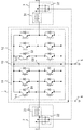
図1は本発明の実施の形態1における電力変換装置を示す回路図である。
図1において、符号1は交流電源から受電した交流電圧を直流電圧に変換し、得られた直流電圧を安定した交流電圧に変換する変換器、2は変換器1の入力側に設けられたフィルタ、3は変換器1の出力側に設けられたフィルタである。また、4は変換器1と接地点との間に存在する浮遊容量である。
FIG. 1 is a circuit diagram showing a power conversion apparatus according to
In FIG. 1,
変換器1は、交流電源から受電してこれを直流電圧に一旦変換するコンバータ11と、コンバータ11で得られた直流電圧を安定化した交流電圧に変換して負荷に供給するインバータ12とを備え、コンバータ11とインバータ12との間には、コンデンサC0からなる電圧平滑回路13が設けられている。
The
コンバータ11は、スイッチング素子Tr1とダイオードD1とを有する3相フルブリッジ回路からなり、また、インバータ12は、スイッチング素子Tr2とダイオードD2とを有する3相フルブリッジ回路で構成されている。そして、各スイッチング素子Tr1,Tr2が図示しない制御回路によってスイッチングされる。
また、上記の入力側のフィルタ2は、コンバータ11を構成するスイッチング素子Tr1のスイッチングに伴って発生するキャリア周波数成分の影響が電源系統側に伝わらないように、また、出力側のフィルタ3は、インバータ12を構成するスイッチング素子Tr2のスイッチングに伴って発生するキャリア周波数成分の影響が負荷側に伝わらないように、それぞれのキャリア周波数を低減するものであって、入力側のフィルタ2は、リアクトル21とコンデンサ22とから構成され、同様に、出力側のフィルタ3もリアクトル31とコンデンサ32とから構成されている。
Further, the above-mentioned filter 2 on the input side is configured so that the influence of the carrier frequency component generated by switching of the switching element Tr1 constituting the
そして、この実施の形態1の特徴として、入力側のフィルタ2を構成するコンデンサ22の共通接続点と出力側のフィルタ3を構成するコンデンサ32の共通接続点とを互いに電気的に接続すると共に、その接続点と接地点との間にバイパス用のコンデンサ5が接続されている。この場合、後述するように変換器1から浮遊容量4を介して漏洩する高周波電流がバイパス用のコンデンサ5をバイパスして優先的に流れるようにインピーダンスを低くする必要があることから、バイパス用のコンデンサ5は変換器1と接地点との間に生じる浮遊容量4と同等以上の静電容量を持つように設定されている。
As a feature of the first embodiment, the common connection point of the
上記構成の電力変換装置において、変換器1を構成するコンバータ11やインバータ12のスイッチング素子Tr1,Tr2のスイッチングに伴って生じた高周波電流が、変換器1と接地点との間に存在する浮遊容量4を介して流れたとしても、その高周波電流は直ちにバイパス用のコンデンサ5を経由して入力側のフィルタ2あるいは出力側のフィルタ3から変換器1に向けて流れる。そのため、従来のように、浮遊容量4を介して接地点に漏洩した高周波電流が電源系統側の接地点から入力側のフィルタ2を経由して再び変換器1に流入して循環したり、あるは、浮遊容量4を介して接地点に漏洩した高周波電流が負荷側の接地点から出力側のフィルタ3を経由して再び変換器1に流入して循環するといった現象が生じるのが抑制される。
In the power conversion device configured as described above, the high-frequency current generated by switching of the switching elements Tr1 and Tr2 of the
このように、この実施の形態1では、変換器1のスイッチングに伴う高周波電流が電源系統側の接地点や負荷側の接地点を経由するノイズ電流として流れるのを抑制することができるので、電源系統側に接続される他の機器へ誘導障害を与えたり、ラジオ周波数帯に影響を及ぼすなどの不具合発生を防止することができる。
Thus, in this
また、入力側のフィルタ2のコンデンサ22の共通接続点と出力側のフィルタ3のコンデンサ32の共通接続点とをそれぞれ電気的に接続した配線をバイパス用のコンデンサ5を介して接地するため、各フィルタ2,3のコンデンサ22,32の共通接続点を直接に接地する場合に比べて、全体の静電容量の調整が容易である。すなわち、各フィルタ2,3に対して、バイパス用のコンデンサ5がそれぞれ直列に接続されているため、バイパス用のコンデンサ5の静電容量を適切に設定することにより、バイパスしたい比較的高周波の漏洩電流のみがバイパス用のコンデンサ5を介して流れ、低周波の漏洩電流は流れにくくすることができる。これにより、装置から電源系統側、または負荷側へ流れる不要な漏洩電流を効率良く低減することができる。
Further, since the wiring electrically connecting the common connection point of the
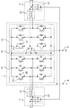
実施の形態2.
図2は本発明の実施の形態2における電力変換装置を示す回路図であり、図1に示した実施の形態1と対応する構成部分には同一の符号を付す。
Embodiment 2. FIG.
FIG. 2 is a circuit diagram showing a power conversion apparatus according to Embodiment 2 of the present invention, and components corresponding to those in
この実施の形態2における電力変換装置の特徴は、入力側のフィルタ2の前段、および出力側のフィルタ3の後段にそれぞれ、3相分の配線が挿通されるコモンモードコア6,7が設けられていることである。このコモンモードコア6,7は、例えばリング状のフェライトコアからなる。その他の構成は、図1に示した実施の形態1と同様であるから、ここでは詳しい説明を省略する。 The power converter according to the second embodiment is characterized in that common mode cores 6 and 7 through which wirings for three phases are inserted are respectively provided in the front stage of the input side filter 2 and the rear stage of the output side filter 3. It is that. The common mode cores 6 and 7 are, for example, ring-shaped ferrite cores. Since the other configuration is the same as that of the first embodiment shown in FIG. 1, detailed description is omitted here.
この実施の形態2では、バイパス用のコンデンサ5に加えて、入力側のフィルタ2の前段にコモンモードコア6を設けることにより、バイパス用のコンデンサ5をバイパスせずに電源系統側の接地点、および負荷側の接地点をそれぞれ経由して流れる一部残留した高周波電流の経路に対してインピーダンスを高くすることができる。これにより、これらの残留した高周波電流が循環するのをさらに抑制することができ、電源系統側に接続される他の機器へ誘導障害を与えたり、ラジオ周波数帯に影響を及ぼすなどの不具合発生を一層効果的に防止することができる。
その他の作用、効果は、実施の形態1の場合と同様であるから、ここでは詳しい説明を省略する。
In the second embodiment, a common mode core 6 is provided in front of the input-side filter 2 in addition to the
Since other operations and effects are the same as those in the first embodiment, detailed description thereof is omitted here.
なお、この実施の形態2では、入力側と出力側の双方にコモンモードコア6,7を設けているが、必要に応じていずれか一方のみを設けることも可能である。 In the second embodiment, the common mode cores 6 and 7 are provided on both the input side and the output side. However, only one of them may be provided as necessary.
実施の形態3.
図3は本発明の実施の形態3における電力変換装置を示す回路図であり、図1に示した実施の形態1と対応する構成部分には同一の符号を付す。
Embodiment 3 FIG.
FIG. 3 is a circuit diagram showing a power conversion device according to Embodiment 3 of the present invention, and the same reference numerals are given to the components corresponding to those of
この実施の形態3の電力変換装置の特徴は、変換器1を構成する電圧平滑回路13とインバータ12との間の直流母線に蓄電池14が並列に接続されていることである。
A feature of the power conversion device of the third embodiment is that a
この蓄電池14は、無停電電源装置(UPS)としての役目を果たすもので、交流電源が正常時には、コンバータ11のスイッチング素子Tr1がスイッチングされて電圧平滑回路13からの直流電圧により蓄電池14が充電される一方、交流電源の停電時にはコンバータ11の動作を停止させて蓄電池14からインバータ12に電力供給を行い、負荷に安定した安定した交流電力を供給する。
The
この蓄電池14を設けた場合にも、蓄電池14と接地点間に浮遊容量が生じるため(特に、変換器1と蓄電池14との配線間距離が長くなるような場合)、この浮遊容量を介して変換器1のスイッチングに伴って生じる高周波電流が漏洩して流れる。しかし、この場合においても、バイパス用のコンデンサ5の静電容量が、変換器1と接地点との間に生じる浮遊容量と蓄電池と接地点との間に生じる浮遊容量との和よりも大きくなるように設定されており、漏洩した高周波電流をバイパス用のコンデンサ5によってバイパスすることができるので、変換器1のスイッチングに伴う高周波電流が電源系統側の接地点や負荷側の接地点を介して流れるのを抑制することができる。これにより、電源系統側に接続される他の機器へ誘導障害を与えたり、ラジオ周波数帯に影響を及ぼすなどの不具合発生を防止することができる。
その他の構成、および作用効果は、実施の形態1の場合と同様であるから、ここでは詳しい説明は省略する。
Even when the
Other configurations and operational effects are the same as those of the first embodiment, and thus detailed description thereof is omitted here.
本発明は、上記の実施の形態1〜3の構成に限定されるものではなく、その趣旨を逸脱しない範囲内において各種の変形を加えることが可能である。
例えば、上記の各実施の形態1〜3では、変換器1において電源系統の交流電圧を直流電圧に変換する際に、スイッチング素子として、図ではIGBT(Insulated Gate Bipolar Transistor)により構成しているが、これに限らず、トランジスタやMOSFET(Metal Oxide Semiconductor Field Effect Transistor)に代替しても同様の効果を得ることができる。
The present invention is not limited to the configurations of the first to third embodiments, and various modifications can be made without departing from the spirit of the present invention.
For example, in each of the first to third embodiments, when the
また、各実施の形態1〜3では、入力側と出力側の各フィルタ2,3のコンデンサ22,32の共通接続点をそれぞれ電気的に接続した配線にはバイパス用のコンデンサ5以外は接続していないが、これに限らず、例えば図4に示すように、変換器1の直流母線にバイパス用のコンデンサ5を同時に接続しても同様の効果が得られる。また、図5に示すように、電圧平滑回路13を構成する2つのコンデンサC1,C2の中点にバイパス用のコンデンサ5を同時に接続しても同様の効果を得ることができる。
Further, in each of the first to third embodiments, except for the
1 変換器、11 コンバータ、12 インバータ、13 電圧平滑回路、
14 蓄電池、2 入力側のフィルタ、3 出力側のフィルタ、4 浮遊容量、
5 バイパス用のコンデンサ、6,7 コモンモードコア。
1 converter, 11 converter, 12 inverter, 13 voltage smoothing circuit,
14 storage battery, 2 input filter, 3 output filter, 4 stray capacitance,
5 Capacitor for bypass, 6, 7 Common mode core.
Claims (5)
上記入力側のフィルタを構成するコンデンサの共通接続点と上記出力側のフィルタを構成するコンデンサの共通接続点とを互いに電気的に接続すると共に、その接続点と接地点との間にバイパス用のコンデンサを接続していることを特徴とする電力変換装置。 A converter that receives power from an AC power source to obtain a DC voltage and converts the DC voltage into an AC voltage, a filter connected to the input side of the converter, and a filter connected to the output side of the converter In the power converter provided,
The common connection point of the capacitor constituting the filter on the input side and the common connection point of the capacitor constituting the filter on the output side are electrically connected to each other, and the bypass is connected between the connection point and the ground point. A power converter characterized by connecting a capacitor.
Priority Applications (1)
| Application Number | Priority Date | Filing Date | Title |
|---|---|---|---|
| JP2008185584A JP5279381B2 (en) | 2008-07-17 | 2008-07-17 | Power converter |
Applications Claiming Priority (1)
| Application Number | Priority Date | Filing Date | Title |
|---|---|---|---|
| JP2008185584A JP5279381B2 (en) | 2008-07-17 | 2008-07-17 | Power converter |
Publications (2)
| Publication Number | Publication Date |
|---|---|
| JP2010028942A true JP2010028942A (en) | 2010-02-04 |
| JP5279381B2 JP5279381B2 (en) | 2013-09-04 |
Family
ID=41734215
Family Applications (1)
| Application Number | Title | Priority Date | Filing Date |
|---|---|---|---|
| JP2008185584A Active JP5279381B2 (en) | 2008-07-17 | 2008-07-17 | Power converter |
Country Status (1)
| Country | Link |
|---|---|
| JP (1) | JP5279381B2 (en) |
Cited By (5)
| Publication number | Priority date | Publication date | Assignee | Title |
|---|---|---|---|---|
| JP2011147252A (en) * | 2010-01-14 | 2011-07-28 | Mitsubishi Electric Corp | Uninterruptible power supply apparatus |
| WO2015184113A1 (en) * | 2014-05-29 | 2015-12-03 | Eaton Corporation | System and method for safe switching in an ac-to-ac converter |
| JP2016171697A (en) * | 2015-03-13 | 2016-09-23 | 多摩川精機株式会社 | Drive circuit and method of brushless dc motor |
| WO2017125154A1 (en) * | 2016-01-21 | 2017-07-27 | Vacon Oy | Frequency converter with lcl line and common mode filter |
| JP2021145543A (en) * | 2020-03-12 | 2021-09-24 | シェンヂェン ヴイマックス ニュー エネルギー カンパニー リミテッドShenzhen VMAX New Energy Co., Ltd. | Single three-phase charging combination type conversion circuit and on-vehicle charging machine |
Families Citing this family (1)
| Publication number | Priority date | Publication date | Assignee | Title |
|---|---|---|---|---|
| CN113544965B (en) * | 2019-03-11 | 2024-03-26 | 港大科桥有限公司 | AC to DC and DC to AC power conversion |
Citations (4)
| Publication number | Priority date | Publication date | Assignee | Title |
|---|---|---|---|---|
| JPH09285115A (en) * | 1996-04-11 | 1997-10-31 | Nemic Lambda Kk | Power source equipment |
| JPH09294381A (en) * | 1996-04-25 | 1997-11-11 | Hitachi Ltd | Input/output non-insulating power converter |
| JP2001069762A (en) * | 1999-08-31 | 2001-03-16 | Mitsubishi Electric Corp | Leak current reducing filter for inverter type driver |
| JP2005130575A (en) * | 2003-10-22 | 2005-05-19 | Yaskawa Electric Corp | Noise filter and motor driving device |
-
2008
- 2008-07-17 JP JP2008185584A patent/JP5279381B2/en active Active
Patent Citations (4)
| Publication number | Priority date | Publication date | Assignee | Title |
|---|---|---|---|---|
| JPH09285115A (en) * | 1996-04-11 | 1997-10-31 | Nemic Lambda Kk | Power source equipment |
| JPH09294381A (en) * | 1996-04-25 | 1997-11-11 | Hitachi Ltd | Input/output non-insulating power converter |
| JP2001069762A (en) * | 1999-08-31 | 2001-03-16 | Mitsubishi Electric Corp | Leak current reducing filter for inverter type driver |
| JP2005130575A (en) * | 2003-10-22 | 2005-05-19 | Yaskawa Electric Corp | Noise filter and motor driving device |
Cited By (8)
| Publication number | Priority date | Publication date | Assignee | Title |
|---|---|---|---|---|
| JP2011147252A (en) * | 2010-01-14 | 2011-07-28 | Mitsubishi Electric Corp | Uninterruptible power supply apparatus |
| WO2015184113A1 (en) * | 2014-05-29 | 2015-12-03 | Eaton Corporation | System and method for safe switching in an ac-to-ac converter |
| US9425702B2 (en) | 2014-05-29 | 2016-08-23 | Eaton Corporation | System and method for safe switching in an AC-to-AC converter |
| JP2016171697A (en) * | 2015-03-13 | 2016-09-23 | 多摩川精機株式会社 | Drive circuit and method of brushless dc motor |
| WO2017125154A1 (en) * | 2016-01-21 | 2017-07-27 | Vacon Oy | Frequency converter with lcl line and common mode filter |
| US10270367B2 (en) | 2016-01-21 | 2019-04-23 | Vacon Oy | Frequency converter with LCL line and common mode filter |
| JP2021145543A (en) * | 2020-03-12 | 2021-09-24 | シェンヂェン ヴイマックス ニュー エネルギー カンパニー リミテッドShenzhen VMAX New Energy Co., Ltd. | Single three-phase charging combination type conversion circuit and on-vehicle charging machine |
| JP7126725B2 (en) | 2020-03-12 | 2022-08-29 | シェンヂェン ヴイマックス ニュー エネルギー カンパニー リミテッド | Single-phase three-phase charging combined conversion circuit and on-board charger |
Also Published As
| Publication number | Publication date |
|---|---|
| JP5279381B2 (en) | 2013-09-04 |
Similar Documents
| Publication | Publication Date | Title |
|---|---|---|
| JP5279381B2 (en) | Power converter | |
| US8472215B2 (en) | Grid-tie inverter for interconnecting AC voltage to electric power grid | |
| EP2352223B1 (en) | System interconnection inverter | |
| RU2416867C1 (en) | Electric energy conversion device for electrically driven car | |
| US9887641B2 (en) | Power converter | |
| JP5237308B2 (en) | Uninterruptible power system | |
| JP2010288381A (en) | Noise reduction circuit of power conversion equipment | |
| JP6771693B1 (en) | Power converter | |
| JP2007325377A (en) | Power conversion device | |
| JP2009148078A (en) | Noise filter | |
| JP2016025713A (en) | Power supply device | |
| JP2007181341A (en) | Converter device | |
| JPWO2016027374A1 (en) | Power converter | |
| JP2006507714A (en) | Active common mode EMI filter with series cascaded filter with reduced power consumption and transistor rated voltage | |
| JP2009296798A (en) | Power conversion apparatus | |
| US10090753B1 (en) | Power conversion device and power conversion system | |
| JP2016158316A (en) | Power supply device | |
| JP5378244B2 (en) | Power converter | |
| JP2010063284A (en) | Power conversion device and power conversion system | |
| JP2002272113A (en) | Dc reactor device and high-frequency suppression control device | |
| JP2015053835A (en) | Noise filter | |
| JP4765754B2 (en) | Transformerless inverter device | |
| JP2010158125A (en) | Dc power supply apparatus and reactor apparatus | |
| JPWO2021024455A1 (en) | Power conversion system | |
| JP5676990B2 (en) | Switching method for power converter |
Legal Events
| Date | Code | Title | Description |
|---|---|---|---|
| A621 | Written request for application examination |
Free format text: JAPANESE INTERMEDIATE CODE: A621 Effective date: 20101104 |
|
| A977 | Report on retrieval |
Free format text: JAPANESE INTERMEDIATE CODE: A971007 Effective date: 20120725 |
|
| A131 | Notification of reasons for refusal |
Free format text: JAPANESE INTERMEDIATE CODE: A131 Effective date: 20120801 |
|
| A521 | Request for written amendment filed |
Free format text: JAPANESE INTERMEDIATE CODE: A523 Effective date: 20120924 |
|
| A02 | Decision of refusal |
Free format text: JAPANESE INTERMEDIATE CODE: A02 Effective date: 20130212 |
|
| A521 | Request for written amendment filed |
Free format text: JAPANESE INTERMEDIATE CODE: A523 Effective date: 20130419 |
|
| A911 | Transfer to examiner for re-examination before appeal (zenchi) |
Free format text: JAPANESE INTERMEDIATE CODE: A911 Effective date: 20130426 |
|
| TRDD | Decision of grant or rejection written | ||
| A01 | Written decision to grant a patent or to grant a registration (utility model) |
Free format text: JAPANESE INTERMEDIATE CODE: A01 Effective date: 20130521 |
|
| A61 | First payment of annual fees (during grant procedure) |
Free format text: JAPANESE INTERMEDIATE CODE: A61 Effective date: 20130521 |
|
| R150 | Certificate of patent or registration of utility model |
Free format text: JAPANESE INTERMEDIATE CODE: R150 Ref document number: 5279381 Country of ref document: JP Free format text: JAPANESE INTERMEDIATE CODE: R150 |
|
| R250 | Receipt of annual fees |
Free format text: JAPANESE INTERMEDIATE CODE: R250 |
|
| R250 | Receipt of annual fees |
Free format text: JAPANESE INTERMEDIATE CODE: R250 |
|
| R250 | Receipt of annual fees |
Free format text: JAPANESE INTERMEDIATE CODE: R250 |
|
| R250 | Receipt of annual fees |
Free format text: JAPANESE INTERMEDIATE CODE: R250 |
|
| R250 | Receipt of annual fees |
Free format text: JAPANESE INTERMEDIATE CODE: R250 |
|
| R250 | Receipt of annual fees |
Free format text: JAPANESE INTERMEDIATE CODE: R250 |
|
| R250 | Receipt of annual fees |
Free format text: JAPANESE INTERMEDIATE CODE: R250 |
|
| R250 | Receipt of annual fees |
Free format text: JAPANESE INTERMEDIATE CODE: R250 |
|
| R250 | Receipt of annual fees |
Free format text: JAPANESE INTERMEDIATE CODE: R250 |