JP2004222296A - Clock signal generating system - Google Patents
Clock signal generating system Download PDFInfo
- Publication number
- JP2004222296A JP2004222296A JP2004007252A JP2004007252A JP2004222296A JP 2004222296 A JP2004222296 A JP 2004222296A JP 2004007252 A JP2004007252 A JP 2004007252A JP 2004007252 A JP2004007252 A JP 2004007252A JP 2004222296 A JP2004222296 A JP 2004222296A
- Authority
- JP
- Japan
- Prior art keywords
- clock signal
- signal
- clock
- signals
- circuit
- Prior art date
- Legal status (The legal status is an assumption and is not a legal conclusion. Google has not performed a legal analysis and makes no representation as to the accuracy of the status listed.)
- Withdrawn
Links
Images


Classifications
-
- G—PHYSICS
- G06—COMPUTING; CALCULATING OR COUNTING
- G06F—ELECTRIC DIGITAL DATA PROCESSING
- G06F1/00—Details not covered by groups G06F3/00 - G06F13/00 and G06F21/00
- G06F1/04—Generating or distributing clock signals or signals derived directly therefrom
- G06F1/08—Clock generators with changeable or programmable clock frequency
-
- H—ELECTRICITY
- H03—ELECTRONIC CIRCUITRY
- H03K—PULSE TECHNIQUE
- H03K21/00—Details of pulse counters or frequency dividers
- H03K21/08—Output circuits
- H03K21/10—Output circuits comprising logic circuits
Abstract
Description
本発明は、一般に、ディジタル回路要素に関するものであり、とりわけ、クロック分周回路に関するものである。 The present invention relates generally to digital circuit elements, and more particularly to a clock divider circuit.
ディジタル・システムの構成要素は、一般に、システム・クロックを用いて動作する。システム・クロックによって、構成要素内のディジタル回路の同期がとられ、ディジタル回路による情報の生成及び処理が可能になる。それぞれ異なる時間に、ディジタル・システム内の異なる構成要素によって、異なる周波数及び/またはデューティ・サイクルのクロック信号が利用される可能性がある。異なる周波数及び/またはデューティ・サイクルのクロック信号を発生するため、システムに複数クロックを組み込むことも可能であるが、システムに複数クロックを設けるのは、システム設計にとってコスト、複雑性、または、物理的スペースの増大につながる可能性がある。結果として、ディジタル・システムにおいて、複数クロックを用いて、異なる周波数及び/またはデューティ・サイクルでクロック信号を発生するのは望ましくない。 Components of a digital system generally operate using a system clock. The system clock synchronizes digital circuitry within the component and allows the digital circuitry to generate and process information. At different times, different components in the digital system may utilize clock signals of different frequencies and / or duty cycles. Multiple clocks can be incorporated into the system to generate clock signals of different frequencies and / or duty cycles, but having multiple clocks in the system is costly, complex, or physically expensive for the system design. May lead to increased space. As a result, it is undesirable in digital systems to use multiple clocks to generate clock signals at different frequencies and / or duty cycles.
さまざまなアナログまたはディジタル回路を用いて、クロック信号の周波数またはデューティ・サイクルを変更することが可能である。しかし、これらの回路では、特定のディジタル・システムにとって望ましい周波数及び/またはデューティ・サイクルのクロック信号を発生することができない。例えば、これらの回路では、分周クロック信号の周波数が、システム・クロックの周波数の奇数分の1(例えば、1/3、1/5、1/7等)である場合、デューティ・サイクルが50%の分周クロック信号を発生することができない。さらに、これらの回路は、それぞれ異なる時間に、クロック信号の周波数を変更することができるように、プログラムすることが不可能である。 Various analog or digital circuits can be used to change the frequency or duty cycle of the clock signal. However, these circuits cannot generate a clock signal of a frequency and / or duty cycle that is desirable for a particular digital system. For example, in these circuits, if the frequency of the divided clock signal is an odd fraction of the frequency of the system clock (eg, 1/3, 1/5, 1/7, etc.), the duty cycle will be 50. % Divided clock signal cannot be generated. Furthermore, these circuits cannot be programmed such that the frequency of the clock signal can be changed at different times.
本発明の目的は、一のクロック信号の周波数の分数である周波数を有するクロック信号を広範囲に発生することにある。 It is an object of the present invention to generate a clock signal having a frequency that is a fraction of the frequency of one clock signal over a wide range.
本発明によれば、第1のクロック信号に応答して、符号化信号の第1の組を発生するように構成された第1の回路と、第1のクロック信号に応答して、符号化信号の第2の組を発生するように構成された第2の回路を含むシステムが得られる。このシステムには、符号化信号の第1の組及び符号化信号の第2の組に応答して、第1のパルス信号及び第2のパルス信号を発生するように構成された第3の回路と、第1のパルス信号及び第2のパルス信号に応答して、第2のクロック信号を発生するように構成された第4の回路も含まれている。 According to the present invention, a first circuit configured to generate a first set of encoded signals in response to a first clock signal, and an encoding circuit responsive to the first clock signal. A system is provided that includes a second circuit configured to generate a second set of signals. The system includes a third circuit configured to generate a first pulse signal and a second pulse signal in response to the first set of encoded signals and the second set of encoded signals. And a fourth circuit configured to generate a second clock signal in response to the first pulse signal and the second pulse signal.
望ましい実施態様に関する下記の詳細な説明では、その一部をなしている、本発明の実施が可能な特定の実施態様を例証するために示された添付の図面を参照する。もちろん、他の実施態様を利用することも可能であり、あるいは、本発明の範囲を逸脱することなく、構造または論理上の変更を加えることも可能である。従って、以下の詳細な説明は、制限の意味にとるべきではなく、本発明の範囲は付属の請求項によって定義される。 In the following detailed description of the preferred embodiments, reference is made to the accompanying drawings that form a part hereof, and in which is shown by way of illustration specific embodiments in which the invention may be practiced. Of course, other embodiments may be utilized, or structural or logical changes may be made without departing from the scope of the invention. Therefore, the following detailed description is not to be taken in a limiting sense, and the scope of the present invention is defined by the appended claims.
本明細書では、クロック分周回路が解説され、例示される。クロック分周回路は、システム・クロック信号のような第1のクロック信号を受信し、第1のクロック信号を用いて、第2のクロック信号を発生する。第2のクロック信号は、デューティ・サイクルが50%で、周波数が、第1のクロック信号の周波数の1/nであるが、ここで、nは1以上の整数である。すなわち、nを3、5、または、7のような奇数にして、第2のクロック信号の周波数を、それぞれ、第1のクロック信号の1/3、1/5、または、1/7にすることが可能である。一部の実施態様では、nの値を経時変化させえるように、クロック分周回路をプログラムできる。 In this specification, a clock divider circuit is described and exemplified. The clock divider receives a first clock signal, such as a system clock signal, and uses the first clock signal to generate a second clock signal. The second clock signal has a duty cycle of 50% and a frequency that is 1 / n of the frequency of the first clock signal, where n is an integer greater than or equal to one. That is, n is set to an odd number such as 3, 5, or 7, and the frequency of the second clock signal is set to 1/3, 1/5, or 1/7 of the first clock signal, respectively. It is possible. In some embodiments, the clock divider can be programmed so that the value of n can change over time.
下記の図には、ハードウェア論理素子を用いたクロック分周回路の実施態様が例示されている。本明細書に示されていない他の実施態様には、ソフトウェア、または、ハードウェアとソフトウェアの組合せを用いて、クロック分周回路の1つ以上の機能を実施することが可能なものもある。 The following figure illustrates an embodiment of a clock divider circuit using hardware logic elements. Other embodiments not shown herein may implement one or more functions of the clock divider circuit using software or a combination of hardware and software.
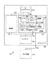
図1は、クロック分周回路150を含むシステム100の実施態様を例示したブロック図である。図示のように、図1には、トランシーバ120に結合されたホスト装置110が含まれている。トランシーバ120には、送信機122、受信機124、コントローラ126、及び、光インターフェイス128が含まれている。送信機122には、レーザ140、PINフォトダイオード142、増幅器144、アナログ・ディジタル変換器(AD変換器)146、システム・クロック148、及び、クロック分周回路150が含まれている。
FIG. 1 is a block diagram illustrating an embodiment of a
ホスト装置110は、トランシーバ120と連係動作するように構成された任意のタイプの有線または無線装置とすることが可能である。こうした装置の例には、サーバ・コンピュータ・システム、パーソナル・コンピュータ・システム、ラップ・トップ・コンピュータ・システム、ハンド・ヘルド・コンピュータ・システム、携帯端末、及び、携帯電話が含まれている。
トランシーバ120には、電気的接続152を用いて、ディジタル信号を送受信することにより、ホスト装置110との通信を行うように構成された光トランシーバが含まれている。電気的接続152によって、ホスト装置110と送信機122が結合されるが、電気的接続152は、任意の適合する直列または並列接続とすることが可能である。適合する接続の1つは、Philips Semiconductorsから入手可能なI2C−Bus Specificationに規定されている、I2C接続ということになる。トランシーバ120は、光インターフェイス128を用いて光信号を送受信することによって、別の装置(不図示)とも通信を行う。光インターフェイス128は、光ファイバ・チャネル・インターフェイスまたは別のタイプの光インターフェイスとすることが可能である。
Transceiver 120 includes an optical transceiver configured to communicate with
実施態様の1つでは、トランシーバ120は、SFP(小形差込可能)トランシーバに関するSFF−8074i規格に適合している。SFF−8074i規格は、http://www.sffcommitte.com、または、ftp://ftp.seagate.com/sff/で入手可能である。他の実施態様では、トランシーバ120は、他の規格に適合可能である。
In one embodiment,
送信機122は、図1に示されていない接続を用いて、ホスト110からディジタル出力信号を受信し、ディジタル・アナログ変換器(不図示)を用いて、ディジタル出力信号をアナログ出力信号に変換し、アナログ出力信号をレーザ140に供給する。レーザ140は、アナログ出力信号に応答して、光出力信号を発生し、光出力信号を光インターフェイス128に供給する。
受信機124は、接続156を用いて、光インターフェイス128から光入力信号を受信し、アナログ・ディジタル変換器(不図示)を用いて、光入力信号をディジタル入力信号に変換し、図1には示されていない接続を用いて、ディジタル入力信号をホスト110に供給する。
コントローラ126は、接続158を用いて、送信機122及び受信機124に制御信号を送り、それらからフィードバック信号を受信する。接続158は、任意の適合する直列または並列接続とすることが可能である。適合する接続の1つは、Philips Semiconductorsから入手可能なI2C−Bus Specificationに規定されている、I2C接続ということになる。コントローラ126には、制御信号を発生して、フィードバック信号を受信する、マイクロコントローラ、ファームウェア、及び、メモリ(不図示)が含まれる。
動作時、PINフォトダイオード142は、接続162を用いて、レーザ140から光信号を受信する。PINフォトダイオード142は、光信号をアナログ信号に変換し、接続164を介して、アナログ信号を増幅器144に供給する。増幅器144は、アナログ信号を増幅し、接続166を介して、増幅信号をアナログ・ディジタル変換器146に供給する。アナログ・ディジタル変換器146には、アナログ信号をディジタル信号に変換し、接続158を介して、ディジタル信号をコントローラ126に供給するように構成されたシグマ・デルタ変調器が含まれている。コントローラ126は、ディジタル信号の受信に応答し、接続158を介して、制御信号をレーザ140に供給する。PINフォトダイオード142、増幅器144、及び/または、アナログ・ディジタル変換器146は、モニタ回路を構成している。
In operation,
システム・クロック148は、接続168を用いて、システム・クロック信号をクロック分周回路150に供給する。クロック分周回路150は、システム・クロック信号を受信し、システム・クロック信号を用いて、分周クロック信号を発生する。クロック分周回路150は、接続170を用いて、分周クロック信号をアナログ・ディジタル変換器146に供給する。
分周クロック信号の周波数は、システム・クロック信号の周波数の1/nであるが、ここで、nは1以上の整数である。nは、1を超える奇整数を含む、1以上の任意の整数とすることが可能である。ある特定の実施態様の場合、nは3であり、従って、分周クロック信号の周波数は、システム・クロック信号の周波数の1/3になる。 The frequency of the divided clock signal is 1 / n of the frequency of the system clock signal, where n is an integer of 1 or more. n can be any integer greater than or equal to one, including odd integers greater than one. In one particular embodiment, n is 3, so the frequency of the divided clock signal is one third of the frequency of the system clock signal.
図1の実施態様の場合、クロック分周回路150は、システム・クロック信号の周波数に基づいて設定された周波数の分周クロック信号を発生するように構成されている。換言すれば、n値は、3のような特定の値に設定され、プログラム可能ではない。下記の図7に関連して後述する別の実施態様の場合、n値は、クロック分周回路が、異なる時間に、それぞれ異なるn値に応答して、分周クロック信号を発生することができるように、プログラム可能である。
In the embodiment of FIG. 1, the
図1の実施態様の場合、送信機122には、システム・クロック148及びクロック分周回路150が含まれている。他の実施態様には、システム・クロック148及びクロック分周回路150をトランシーバ120の他の部分に含むことが可能なものもある。
In the embodiment of FIG. 1, the
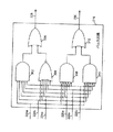
図2は、クロック分周回路150の実施態様のさらなる詳細を例示したブロック図である。クロック分周回路150には、正エッジ・エンコーダ212、負エッジ・エンコーダ214、パルス回路216、及び、クロックト・Dフリップ・フロップ218が含まれている。システム・クロック148から受信するシステム・クロック信号は、接続168を用いて、正エッジ・エンコーダ212及び負エッジ・エンコーダ214に供給される。正エッジ・エンコーダ212は、システム・クロック信号の正エッジすなわち上昇エッジに応答して、符号化信号を1組発生し、接続224a、224b、及び、224cを用いて、この1組の信号をパルス回路216に供給する。正エッジ・エンコーダ212は、3ビット幅の環状シフト・レジスタまたは3ビット幅エンコーダとすることが可能である。負エッジ・エンコーダ214は、システム・クロック信号の負エッジすなわち下降エッジに応答して、符号化信号を1組発生し、接続226a、226b、及び、226cを用いて、この1組の信号をパルス回路216に供給する。負エッジ・エンコーダ214は、3ビット幅の環状シフト・レジスタまたは3ビット幅エンコーダとすることが可能である。パルス回路216は、これらの複数組の符号化信号に応答して、第1及び第2のパルス信号を発生し、接続228及び230を用いて、クロックト・Dフリップ・フロップ218に供給する。接続228は、クロックト・Dフリップ・フロップ218のCLEAR入力に結合され、接続230は、クロックト・Dフリップ・フロップ218のCLOCK入力に結合されている。クロックト・Dフリップ・フロップ218のD入力は、高に結合される、すなわち、論理1すなわち高レベルに設定される。クロックト・Dフリップ・フロップ218は、第1及び第2のパルス信号を受信し、第1及び第2のパルス信号を用いて、分周クロック信号を発生し、Q出力から接続170に分周クロック信号を送り出す。
FIG. 2 is a block diagram illustrating further details of an embodiment of
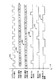
図4は、図2に示すクロック分周回路150によって発生する信号の実施態様を例示したタイム・チャートである。図4には、システム・クロック信号402、符号化信号の第1の組404、符号化信号の第2の組406、第1のパルス信号408、第2のパルス信号410、及び、分周クロック信号412が含まれている。
FIG. 4 is a time chart illustrating an embodiment of a signal generated by
図2及び4を参照すると、正エッジ・エンコーダ212は、システム・クロック148からクロック信号402を受信して、符号化信号の第1の組404を発生する。図4に示すように、符号化信号の第1の組404は、000から始まり、システム・クロック信号402の正エッジに応答して、001、011、111、110、100、000等の順に続く。符号化信号の第1の組404の場合、最上位ビットは、接続224aに対応し、2番目に上位のビットは、接続224bに対応し、最下位ビットは、接続224cに対応する。
Referring to FIGS. 2 and 4,
負エッジ・エンコーダ214は、システム・クロック148からシステム・クロック信号402を受信し、符号化信号の第2の組406を発生する。符号化信号の第2の組406は、システム・クロック信号の負の各エッジ402毎に変化する。符号化信号の第2の組406は、000で始まり、システム・クロック信号402の負エッジに応答して、001、011、111、110、100、000等の順に続く。符号化信号の第2の組406の場合、最上位ビットは、接続226aに対応し、2番目に上位のビットは、接続226bに対応し、最下位ビットは、接続226cに対応する。
図2に示すように、組をなす符号化信号404及び406は、接続224a、224b、224c、226a、226b、及び、226cを用いて、パルス回路216に供給される。図3は、パルス回路216の実施態様を例示した回路図である。図3の場合、接続224a、224b、224c、226a、226b、及び、226cは、図示のように、ANDゲート302、NORゲート304、ANDゲート308、及び、ANDゲート310に結合されている。ANDゲート302及びNORゲート304の出力は、ORゲート306に供給されて、接続228に第1のパルス信号408が生じる。ANDゲート308及びANDゲート310の出力は、ORゲート312に供給されて、接続230に第2のパルス信号410が生じる。同じかまたは異なる数の入力を備えた、他のタイプ及び/または数のゲートを用いて、第1及び第2のパルス信号を発生する多くの回路バリエーションが可能であるので、図3の回路は、例証のために示されたものということになる。
As shown in FIG. 2, sets of encoded
図2及び4を参照すると、第1のパルス信号408は、クロックト・Dフリップ・フロップ218のCLEAR入力に供給され、第2のパルス信号410は、クロックト・Dフリップ・フロップ218のCLOCK入力に供給される。図示のように、D入力が高に結合されると、分周クロック信号412は、クロックト・Dフリップ・フロップ218のQ出力によって送り出される。第1のパルス信号408からの各パルスによって、Q出力がクリアされ、すなわち、論理低レベルに遷移し、第2のパルス信号からの各パルスによって、高レベルのD入力がQ出力に刻時出力され、論理高レベルを生じることになる。結果として、分周クロック信号412は、周波数が、システム・クロック信号の周波数を3で割ったすなわち1/3としたものになり、デューティ・サイクルは50%になる。
Referring to FIGS. 2 and 4, a
図5は、分周クロック信号を発生する方法の実施態様を例示したフローチャートである。図5において、ブロック502に示すように、第1のクロック信号を用いて、符号化信号を複数組発生する。2組の符号化信号を発生することが可能であり、各組毎に、nに等しい数の信号が含まれるが、ここで、nは1以上の整数である。符号化信号の組は、それぞれ、第1のクロック信号の異なる部分を用いて発生することが可能である。例えば、符号化信号の第1の組は、第1のクロック信号の正エッジを用いて発生することが可能であり、符号化信号の第2の組は、第1のクロック信号の負エッジを用いて発生することが可能である。ブロック504に示すように、これら符号化信号の複数組を用いて、パルス信号を発生する。これら複数組の符号化信号に応答して、2つのパルス信号を発生することが可能である。ブロック506に示すように、これらのパルス信号を用いて、第2のクロック信号を発生する。第2のクロック信号は、デューティ・サイクルが50%で、n分周された周波数を有するが、ここで、nは符号化信号の各組における信号数に等しい。従って、第2のクロック信号は、分周クロック信号をなしている。例えば、nが3の場合、第2のクロック信号の周波数は、第1のクロック信号の周波数の1/3になる。
FIG. 5 is a flowchart illustrating an embodiment of a method for generating a divided clock signal. In FIG. 5, as shown by a
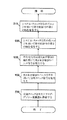
図6は、トランシーバにおいて分周クロック信号を発生する方法の実施態様を例示したフローチャートである。図6において、ブロック602に示すように、システム・クロックの正エッジを用いて、符号化信号の第1の組を発生する。第1の組の信号には、nに等しい数の信号が含まれるが、ここで、nは1以上の整数である。ブロック604に示すように、システム・クロックの負エッジを用いて、符号化信号の第2の組を発生する。第2の組の信号には、nに等しい数の信号が含まれる。ブロック606に示すように、符号化信号の第1及び第2の組を用いて、第1及び第2のパルス信号を発生する。ブロック608に示すように、第1及び第2のパルス信号を用いて、分周クロック信号を発生する。分周クロック信号は、デューティ・サイクルが50%で、周波数がシステム・クロック信号の周波数の1/nである。ブロック610に示すように、分周クロック信号は、アナログ・ディジタル変換器に供給される。 FIG. 6 is a flowchart illustrating an embodiment of a method for generating a divided clock signal in a transceiver. In FIG. 6, the first set of encoded signals is generated using the positive edge of the system clock, as shown at block 602. The first set of signals includes a number of signals equal to n, where n is an integer greater than or equal to one. As shown in block 604, a second set of encoded signals is generated using the negative edge of the system clock. The second set of signals includes a number of signals equal to n. As shown in block 606, first and second sets of encoded signals are used to generate first and second pulse signals. As shown in block 608, a divided clock signal is generated using the first and second pulse signals. The divided clock signal has a duty cycle of 50% and a frequency that is 1 / n of the frequency of the system clock signal. As shown in block 610, the divided clock signal is provided to an analog to digital converter.
図7は、システム・クロック710及びコントローラ720に結合されたプログラマブル・クロック分周回路700の実施態様を例示したブロック図である。クロック分周回路700には、正エッジ・エンコーダ712、負エッジ・エンコーダ714、パルス回路716、及び、クロックト・Dフリップ・フロップ718が含まれている。システム・クロック710からシステム・クロック信号を受信すると、接続722を用いて、正エッジ・エンコーダ712及び負エッジ・エンコーダ714に供給される。正エッジ・エンコーダ712は、システム・クロック信号の正エッジすなわち上昇エッジに応答して、符号化信号を1組発生し、1組の接続724を用いて、この1組の符号化信号をパルス回路716に供給する。正エッジ・エンコーダ712は、nビット幅の環状シフト・レジスタまたはnビット幅エンコーダとすることが可能であるが、ここで、nは1以上の整数である。負エッジ・エンコーダ714は、システム・クロック信号の負エッジすなわち下降エッジに応答して、符号化信号を1組発生し、1組の接続726を用いて、この1組の符号化信号をパルス回路716に供給する。負エッジ・エンコーダ714は、nビット幅の環状シフト・レジスタまたはnビット幅エンコーダとすることが可能であるが、ここで、nは1以上の整数である。パルス回路716は、これらの複数組の符号化信号に応答して、第1及び第2のパルス信号を発生し、接続728及び730を用いて、クロックト・Dフリップ・フロップ718に供給する。接続728は、クロックト・Dフリップ・フロップ718のCLEAR入力に結合され、接続730は、クロックト・Dフリップ・フロップ718のCLOCK入力に結合されている。クロックト・Dフリップ・フロップ718のD入力は、記号731で示すように、高に結合される、すなわち、論理1すなわち高レベルに設定される。クロックト・Dフリップ・フロップ718は、第1及び第2のパルス信号を受信し、第1及び第2のパルス信号を用いて、分周クロック信号を発生し、Q出力から接続732に分周クロック信号を送り出す。
FIG. 7 is a block diagram illustrating an embodiment of a programmable
クロック分周回路700には、コントローラ720からクロック分周信号を受信するように構成されたプログラマブル・クロック分周回路が含まれている。クロック分周回路700は、クロック分周信号に応答して、周波数がシステム・クロック信号の周波数の1/nである分周クロック信号を生じさせるが、ここで、nは1以上の整数であり、クロック分周信号に基づいて決定される。すなわち、コントローラ720からクロック分周回路700に加えられるクロック分周信号によって、分周クロック信号の周波数が設定される。
コントローラ720は、クロック分周信号を発生するために用いられる情報を記憶するか、または、アクセスする。クロック分周信号は、分周クロック信号の周波数を決定する整数nを指示する。コントローラ720は、クロック分周信号を発生し、接続734を用いて、正エッジ・エンコーダ712、負エッジ・エンコーダ714、及び、パルス回路716に加える。
Controller 720 stores or accesses information used to generate the clock divided signal. The clock divided signal indicates an integer n that determines the frequency of the divided clock signal. Controller 720 generates a clock divided signal and applies it to
正エッジ・エンコーダ712は、クロック分周信号に応答して、符号化信号の第1の組を発生する。符号化信号の第1の組には、クロック分周信号によって指示されるn値に等しい数の信号が含まれている。同様に、負エッジ・エンコーダ714は、クロック分周信号に応答して、符号化信号の第2の組を発生する。符号化信号の第2の組には、クロック分周信号によって指示されるn値に等しい数の信号が含まれている。例えば、クロック分周信号によって、nが5であると指示されると、符号化信号の第1、第2の組のそれぞれには、それぞれ、5つの信号が含まれることになる。
パルス回路716は、クロック分周信号及び符号化信号の第1及び第2の組に応答して、第1及び第2のパルス信号を発生し、クロックト・Dフリップ・フロップ718に供給する。上述の図2の実施態様と同様、クロックト・Dフリップ・フロップ718は、第1及び第2のパルス信号に応答して、システム・クロック信号の周波数の1/nの周波数を有する分周クロック信号を発生する。従って、クロック分周信号によって、例えば、nが5であると指示される場合、分周クロック信号は、その周波数がシステム・クロック信号の周波数の1/5になり、デューティ・サイクルが50%になる。
The pulse circuit 716 generates and supplies the first and second pulse signals to the clocked D flip-
望ましい実施態様の説明のため、特定の実施態様について例示し、解説してきたが、当該分野の技術者には明らかなように、本発明の範囲を逸脱することなく、図示及び解説の特定の実施態様の代わりに、同じ目的を実現することを意図した多種多様な代替及び/または同等実施例を用いることも可能である。化学、機械、電気機械、電気、及び、コンピュータの技術者にはすぐ分るように、本発明は、以下に一部をさらに例示するが、多種多様な実施態様で実施可能である。本出願は、本明細書において論述の望ましい実施態様に関するいかなる改変または変更をも網羅することを意図したものである。従って、明らかに、本発明は、請求項及びその同等物による制限しか受けないことを意図したものである。 While specific embodiments have been illustrated and described for purposes of describing the preferred embodiments, it will be apparent to those skilled in the art that specific implementations of the figures and descriptions are possible without departing from the scope of the invention. Instead of the embodiments, a wide variety of alternative and / or equivalent embodiments intended to achieve the same purpose can be used. As will be readily apparent to those of skill in the chemical, mechanical, electromechanical, electrical, and computer arts, the present invention may be embodied in a wide variety of embodiments, some of which are further illustrated below. This application is intended to cover any adaptations or variations of the preferred embodiments discussed herein. Thus, obviously, the present invention is intended to be limited only by the claims and the equivalents thereof.
(実施態様1)
第1のクロック信号を受信し、前記第1のクロック信号の正エッジに応答して、符号化信号の第1の組を発生するように構成された第1の回路(212/712)と、
前記第1のクロック信号を受信し、前記第1のクロック信号の負エッジに応答して、符号化信号の第2の組を発生するように構成された第2の回路(214/714)と、 前記符号化信号の第1の組及び前記符号化信号の第2の組を受信し、前記符号化信号の第1の組及び前記符号化信号の第2の組に応答して、第1のパルス信号及び第2のパルス信号を発生するように構成されている第3の回路(216/716)と、 前記第1のパルス信号及び前記第2のパルス信号を受信し、前記第1のパルス信号及び前記第2のパルス信号に応答して、第2のクロック信号を発生するように構成されている第4の回路(218/718)とを具備する、クロック信号発生システム。
(Embodiment 1)
A first circuit (212/712) configured to receive a first clock signal and generate a first set of encoded signals in response to a positive edge of the first clock signal;
A second circuit (214/714) configured to receive the first clock signal and generate a second set of encoded signals in response to a negative edge of the first clock signal; Receiving a first set of coded signals and a second set of coded signals, and responsive to the first set of coded signals and the second set of coded signals, A third circuit (216/716) configured to generate a first pulse signal and a second pulse signal, the first circuit receiving the first pulse signal and the second pulse signal; A clock signal generation system comprising: a pulse signal; and a fourth circuit (218/718) configured to generate a second clock signal in response to the second pulse signal.
(実施態様2)
前記第1の回路に第1の環状シフト・レジスタが含まれることと、前記第2の回路に第2の環状シフト・レジスタが含まれる、実施態様1に記載のシステム。
(Embodiment 2)
3. The system of claim 1, wherein the first circuit includes a first circular shift register, and the second circuit includes a second circular shift register.
(実施態様3)
前記第1の回路に第1のエンコーダが含まれることと、前記第2の回路に第2のエンコーダが含まれる、実施態様1に記載のシステム。
(Embodiment 3)
The system of claim 1, wherein the first circuit includes a first encoder, and wherein the second circuit includes a second encoder.
(実施態様4)
前記第4の回路に、クロックト・Dフリップ・フロップが含まれる、実施態様1に記載のシステム。
(Embodiment 4)
The system of claim 1, wherein the fourth circuit includes a clocked D flip-flop.
(実施態様5)
前記第1のパルス信号が、前記クロックト・Dフリップ・フロップのクリア入力に加えられることと、前記第2のパルス信号が、前記クロックト・Dフリップ・フロップのクロック入力に加えられることと、前記クロックト・Dフリップ・フロップのD入力が高に結合されることと、前記第2のクロック信号が、前記クロックト・Dフリップ・フロップのQ出力から送り出される、実施態様4に記載のシステム。
(Embodiment 5)
Wherein the first pulse signal is applied to a clear input of the clocked D flip-flop; and the second pulse signal is applied to a clock input of the clocked D flip flop. 5. The system of claim 4, wherein the D input of the clocked D flip flop is tied high and the second clock signal is derived from the Q output of the clocked D flip flop. .
(実施態様6)
前記符号化信号の第1の組と前記符号化信号の第2の組に、それぞれ、nの符号化信号が含まれることと、前記第2のクロック信号の周波数が、前記第1のクロック信号の周波数の1/nであることと、nが1以上の整数である、実施態様1に記載のシステム。
(Embodiment 6)
The first set of coded signals and the second set of coded signals each include n coded signals, and the frequency of the second clock signal is equal to the first clock signal. 2. The system of embodiment 1, wherein the frequency is 1 / n of n, and n is an integer greater than or equal to one.
(実施態様7)
nが1を超える奇整数である、実施態様6に記載のシステム。
(Embodiment 7)
7. The system of embodiment 6, wherein n is an odd integer greater than one.
(実施態様8)
前記第1の回路と前記第2の回路が、それぞれ、整数nを表わすクロック分周信号(734)を受信するように構成されている、実施態様6に記載のシステム。
(Embodiment 8)
7. The system of embodiment 6, wherein the first circuit and the second circuit are each configured to receive a clock divided signal (734) representing an integer n.
(実施態様9):第1のクロック信号を用いて、符号化信号の複数組を発生するステップと、前記符号化信号の複数組を用いて、複数のパルス信号を発生するステップと、前記複数のパルス信号を用いて、第2のクロック信号を発生するステップとを有する、クロック信号発生方法。 (Embodiment 9): generating a plurality of sets of encoded signals using a first clock signal; generating a plurality of pulse signals using the plurality of sets of encoded signals; Generating a second clock signal using the pulse signal of (i).
(実施態様10):前記クロック信号を用いて、前記符号化信号の複数組を発生するステップに、さらに、前記クロック信号の正エッジを用いて、前記符号化信号の複数組のうち符号化信号の第1の組を発生するステップと、前記クロック信号の負エッジを用いて、前記符号化信号の複数組のうち符号化信号の第2の組を発生するステップとを有する、実施態様9に記載の方法。 (Embodiment 10): In the step of using the clock signal to generate a plurality of sets of the coded signals, further using the positive edge of the clock signal, Embodiment 9 comprising: generating a first set of encoded signals; and generating a second set of encoded signals of the plurality of encoded signals using a negative edge of the clock signal. The described method.
(実施態様11):前記符号化信号の複数組が、各組毎に、奇数の信号を備えることを特徴とする、実施態様9に記載の方法。 Embodiment 11: The method according to embodiment 9, wherein the plurality of sets of encoded signals include an odd number of signals for each set.
(実施態様12):さらに、クロック分周信号を受信するステップと、前記クロック分周信号に関連した周波数で前記第2のクロック信号を発生するステップとを有する、実施態様9に記載の方法。 Embodiment 12: The method of embodiment 9, further comprising: receiving a clock divided signal; and generating the second clock signal at a frequency associated with the clock divided signal.
212 第1の回路
214 第2の回路
216 第3の回路
218 第4の回路
712 第1の回路
714 第2の回路
716 第3の回路
718 第4の回路
212
Claims (1)
前記第1のクロック信号を受信し、前記第1のクロック信号の負エッジに応答して、符号化信号の第2の組を発生するように構成された第2の回路と、
前記符号化信号の第1の組及び前記符号化信号の第2の組を受信し、前記符号化信号の第1の組及び前記符号化信号の第2の組に応答して、第1のパルス信号及び第2のパルス信号を発生するように構成されている第3の回路と、
前記第1のパルス信号及び前記第2のパルス信号を受信し、前記第1のパルス信号及び前記第2のパルス信号に応答して、第2のクロック信号を発生するように構成されている第4の回路とを具備する、
クロック信号発生システム。 A first circuit configured to receive a first clock signal and to generate a first set of encoded signals in response to a positive edge of the first clock signal;
A second circuit configured to receive the first clock signal and to generate a second set of encoded signals in response to a negative edge of the first clock signal;
Receiving a first set of the coded signals and a second set of the coded signals, and responsive to the first set of the coded signals and the second set of the coded signals, A third circuit configured to generate a pulse signal and a second pulse signal;
A second pulse signal configured to receive the first pulse signal and the second pulse signal and to generate a second clock signal in response to the first pulse signal and the second pulse signal; And 4 circuits,
Clock signal generation system.
Applications Claiming Priority (1)
| Application Number | Priority Date | Filing Date | Title |
|---|---|---|---|
| US10/346,689 US6856184B2 (en) | 2003-01-15 | 2003-01-15 | Clock divider circuit |
Publications (2)
| Publication Number | Publication Date |
|---|---|
| JP2004222296A true JP2004222296A (en) | 2004-08-05 |
| JP2004222296A5 JP2004222296A5 (en) | 2007-02-22 |
Family
ID=31715568
Family Applications (1)
| Application Number | Title | Priority Date | Filing Date |
|---|---|---|---|
| JP2004007252A Withdrawn JP2004222296A (en) | 2003-01-15 | 2004-01-14 | Clock signal generating system |
Country Status (3)
| Country | Link |
|---|---|
| US (2) | US6856184B2 (en) |
| JP (1) | JP2004222296A (en) |
| GB (1) | GB2397418B (en) |
Families Citing this family (8)
| Publication number | Priority date | Publication date | Assignee | Title |
|---|---|---|---|---|
| US9337948B2 (en) | 2003-06-10 | 2016-05-10 | Alexander I. Soto | System and method for performing high-speed communications over fiber optical networks |
| US7715386B2 (en) * | 2007-03-15 | 2010-05-11 | Microsoft Corporation | Reducing network traffic to teredo server |
| US7764691B2 (en) * | 2007-03-15 | 2010-07-27 | Microsoft Corporation | Allowing IPv4 clients to communicate using teredo addresses when both clients are behind a NAT |
| US8194683B2 (en) * | 2007-03-30 | 2012-06-05 | Microsoft Corporation | Teredo connectivity between clients behind symmetric NATs |
| GB2450564B (en) * | 2007-06-29 | 2011-03-02 | Imagination Tech Ltd | Clock frequency adjustment for semi-conductor devices |
| US8134389B2 (en) * | 2010-03-25 | 2012-03-13 | Apple Inc. | Programmable frequency divider |
| CN102651207B (en) * | 2011-02-22 | 2014-09-24 | 乐金显示有限公司 | Gate driving circuit |
| KR101849571B1 (en) | 2011-02-22 | 2018-05-31 | 엘지디스플레이 주식회사 | Gate driving circuit |
Family Cites Families (14)
| Publication number | Priority date | Publication date | Assignee | Title |
|---|---|---|---|---|
| US4945229A (en) * | 1988-12-29 | 1990-07-31 | Thomas & Betts Corporation | Fiber optic receiver and transceiver |
| US5055800A (en) * | 1990-04-30 | 1991-10-08 | Motorola, Inc. | Fractional n/m synthesis |
| EP0541840B1 (en) * | 1991-11-11 | 1993-07-14 | Hewlett-Packard GmbH | Formatter circuit |
| US5353311A (en) * | 1992-01-09 | 1994-10-04 | Nec Corporation | Radio transmitter |
| US5287296A (en) * | 1992-04-22 | 1994-02-15 | At&T Bell Laboratories | Clock generators having programmable fractional frequency division |
| KR100296832B1 (en) * | 1992-11-13 | 2001-10-24 | 요트.게.아. 롤페즈 | Discrete Time Signal Processing System |
| US5528181A (en) * | 1994-11-02 | 1996-06-18 | Advanced Micro Devices, Inc. | Hazard-free divider circuit |
| US5682605A (en) * | 1994-11-14 | 1997-10-28 | 989008 Ontario Inc. | Wireless communication system |
| JPH09312635A (en) * | 1996-05-21 | 1997-12-02 | Nec Yonezawa Ltd | Clock signal transmitter |
| US6201820B1 (en) * | 1997-03-05 | 2001-03-13 | Silkroad, Inc. | Optically modulated laser beam transceiver |
| DE19719547C1 (en) * | 1997-05-09 | 1998-11-12 | Lucent Tech Network Sys Gmbh | Digital oscillator for desynchronizer in communications system |
| US6487674B1 (en) * | 2000-03-08 | 2002-11-26 | Cirrus Logic, Inc. | Single wire interface for an analog to digital converter |
| US6456164B1 (en) * | 2001-03-05 | 2002-09-24 | Koninklijke Philips Electronics N.V. | Sigma delta fractional-N frequency divider with improved noise and spur performance |
| US6404840B1 (en) * | 2001-06-25 | 2002-06-11 | Agere Systems Inc. | Variable frequency divider |
-
2003
- 2003-01-15 US US10/346,689 patent/US6856184B2/en not_active Expired - Fee Related
-
2004
- 2004-01-06 GB GB0400161A patent/GB2397418B/en not_active Expired - Fee Related
- 2004-01-14 JP JP2004007252A patent/JP2004222296A/en not_active Withdrawn
- 2004-07-15 US US10/892,802 patent/US6914469B2/en not_active Expired - Fee Related
Also Published As
| Publication number | Publication date |
|---|---|
| US6856184B2 (en) | 2005-02-15 |
| US20040135615A1 (en) | 2004-07-15 |
| US20040257138A1 (en) | 2004-12-23 |
| GB2397418B (en) | 2006-09-27 |
| GB2397418A (en) | 2004-07-21 |
| US6914469B2 (en) | 2005-07-05 |
| GB0400161D0 (en) | 2004-02-11 |
Similar Documents
| Publication | Publication Date | Title |
|---|---|---|
| EP2174311B1 (en) | Remote control signaling infrared generator | |
| JP2007104106A (en) | Transmitter/receiver | |
| JP2009528015A (en) | Self-correcting digital pulse width modulator (DPWM) | |
| JP2005304017A (en) | Pulse width modulation system, and pulse width modulation method | |
| TWI641232B (en) | Low power switching techniques for digital-to-analog converters | |
| CN104283664A (en) | Differential decoder | |
| KR20090012212A (en) | Driving laser diodes with immunity to temperature changes, aging, and other effects | |
| US9690399B2 (en) | Signal decoding and modulation processing system for capacitive stylus | |
| JP5343966B2 (en) | Clock signal divider circuit and method | |
| JP2004222296A (en) | Clock signal generating system | |
| TW201640359A (en) | N-base numbers to physical wire states symbols translation method | |
| US20130222165A1 (en) | Integrated Circuit and System Including Current-Based Communication | |
| KR20150120940A (en) | Enhanced numerical controlled oscillator | |
| EP2163998A1 (en) | Cooperation circuit | |
| KR100750894B1 (en) | Symmetric PWM Motor Driving Current Sync. Apparatus using DSP/FPGA | |
| JP3790245B2 (en) | Communication module and communication method for wireless sensor network system | |
| US6711694B1 (en) | Apparatus and method for generating a modulated clock signal including harmonics that exhibit a known sideband configuration | |
| US7114092B2 (en) | Method of supplying a required clock frequency by a clock generator module through interface communication with a mainboard | |
| CN110221996B (en) | Controller configuration method and device in main control chip | |
| JP4464605B2 (en) | Optical transmitter and code conversion circuit used therefor | |
| TWI448071B (en) | System with variably combined common-mode and differential-mode digital output | |
| JP2013009083A (en) | A/d converter | |
| KR100429554B1 (en) | Programmable counter circuit | |
| KR101678770B1 (en) | Device for controlling fractional dither in low jitter digitally controlled oscillator | |
| JPH11150479A (en) | Pulse width signal conversion circuit |
Legal Events
| Date | Code | Title | Description |
|---|---|---|---|
| A521 | Written amendment |
Free format text: JAPANESE INTERMEDIATE CODE: A523 Effective date: 20070109 |
|
| A621 | Written request for application examination |
Free format text: JAPANESE INTERMEDIATE CODE: A621 Effective date: 20070109 |
|
| A711 | Notification of change in applicant |
Free format text: JAPANESE INTERMEDIATE CODE: A711 Effective date: 20070320 |
|
| RD03 | Notification of appointment of power of attorney |
Free format text: JAPANESE INTERMEDIATE CODE: A7423 Effective date: 20070411 |
|
| A761 | Written withdrawal of application |
Free format text: JAPANESE INTERMEDIATE CODE: A761 Effective date: 20070501 |